Embed Size (px)
Citation preview
July 2013 Page 1 of 10
The Basic Principles of Electrical Overstress (EOS)
Application Note
Abstract
With a focus on the LEDs of OSRAM OptoSemiconductors, this application note describesthe basic principles of one of the failure modesof LEDs – electrical overstress (EOS).
Introduction
Every single electronic component or devicehas absolute maximum electrical ratedvalues that are specified by the componentmanufacturer. Each component must beoperated below the maximum rated valuesin order to ensure that it functions properly,reliably, and robustly.As a semiconductor-based optoelectronicdevice, an LED (light-emitting diode) shouldalso be operated below the absolutemaximum electrical ratings specified in themanufacturer's data sheet in order tosafeguard its reliability and service life aswell as to ensure that it is operated safely.One factor that contributes to LED failure inLED circuits and systems is electricaloverstress (EOS). This application notedescribes the nature of EOS, explains how itdiffers from ESD, discusses its causes,outlines EOS-related damage, and provides
information on how an LED can be protectedfrom EOS. Even though these basicprinciples apply to all electronic components,this application note focuses on LEDs.
What is EOS?
Electrical overstress is a term used todescribe an event whereby an electroniccomponent is operated above its absolutemaximum electrical rated values as specifiedin its data sheet. In other words, EOS isexperienced by an electronic componentwhen that component is operated –deliberately or accidentally – above itsabsolute maximum electrical rated values.EOS can be a single event, repeatedevents, or continuous in nature.In the case of an LED, the followingparameters are both relevant and important:Maximum forward current or maximumvoltage across an LED, maximum surgecurrent, maximum reverse current orvoltage, maximum permissible continuouspulse current and temperature. Theseshould all be kept below the maximum ratedvalues to ensure that EOS is notexperienced by the LED.
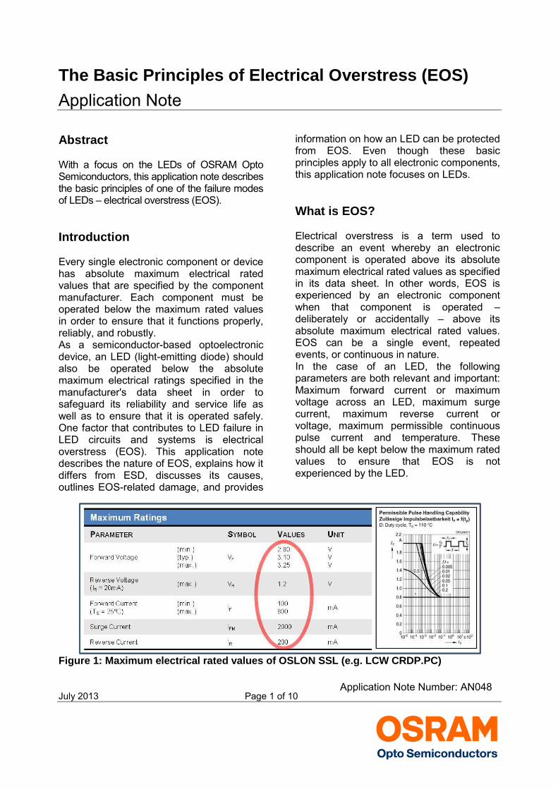
Figure 1: Maximum electrical rated values of OSLON SSL (e.g. LCW CRDP.PC)
Application Note Number: AN048
July 2013 Page 2 of 10
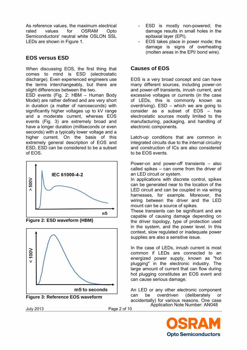
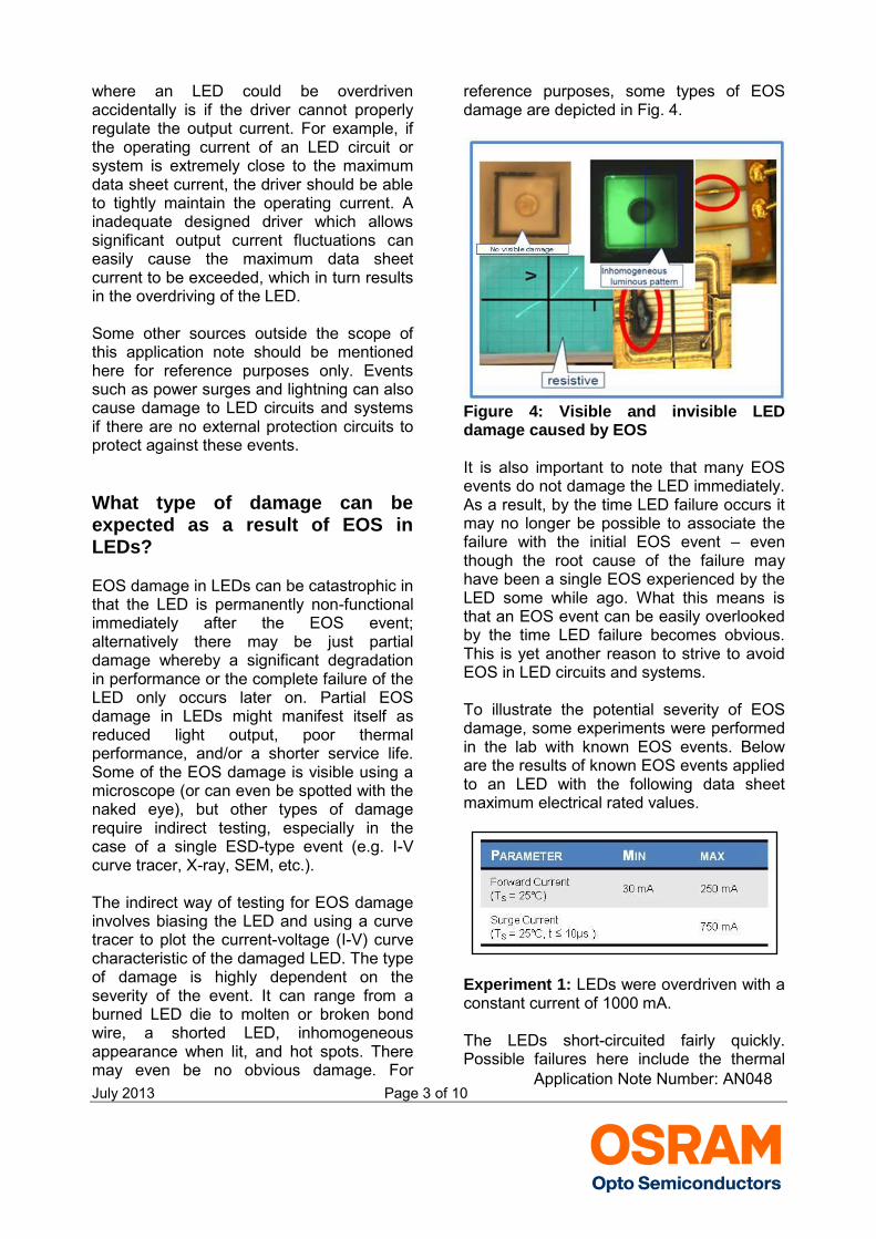
As reference values, the maximum electrical rated values for OSRAM Opto Semiconductors' neutral white OSLON SSL LEDs are shown in Figure 1. EOS versus ESD When discussing EOS, the first thing that comes to mind is ESD (electrostatic discharge). Even experienced engineers use the terms interchangeably, but there are slight differences between the two. ESD events (Fig. 2: HBM – Human Body Model) are rather defined and are very short in duration (a matter of nanoseconds) with significantly higher voltages up to kV range and a moderate current, whereas EOS events (Fig. 3) are extremely broad and have a longer duration (milliseconds or even seconds) with a typically lower voltage and a higher current. On the basis of this extremely general description of EOS and ESD, ESD can be considered to be a subset of EOS.
Figure 2: ESD waveform (HBM)
Figure 3: Reference EOS waveform
- ESD is mostly non-powered; the damage results in small holes in the epitaxial layer (EPI).
- EOS takes place in power mode; the damage is signs of overheating (molten areas in the EPI/ bond wire).
Causes of EOS EOS is a very broad concept and can have many different sources, including power-on and power-off transients, inrush current, and excessive voltages or currents (in the case of LEDs, this is commonly known as overdriving). ESD – which we are going to consider as a subset of EOS – has electrostatic sources mostly limited to the manufacturing, packaging, and handling of electronic components. Latch-up conditions that are common in integrated circuits due to the internal circuitry and construction of ICs are also considered to be EOS events. Power-on and power-off transients – also called spikes – can come from the driver of an LED circuit or system. In applications with discrete control, spikes can be generated near to the location of the LED circuit and can be coupled in via wiring harnesses, for example. Moreover, the wiring between the driver and the LED mount can be a source of spikes. These transients can be significant and are capable of causing damage depending on the driver topology, type of protection used in the system, and the power level. In this context, slow regulated or inadequate power supplies are also a sensitive issue. In the case of LEDs, inrush current is most common if LEDs are connected to an energized power supply, known as "hot plugging" in the electronic industry. The large amount of current that can flow during hot plugging constitutes an EOS event and can cause serious damage. An LED or any other electronic component can be overdriven (deliberately or accidentally) for various reasons. One case
Application Note Number: AN048
July 2013 Page 3 of 10
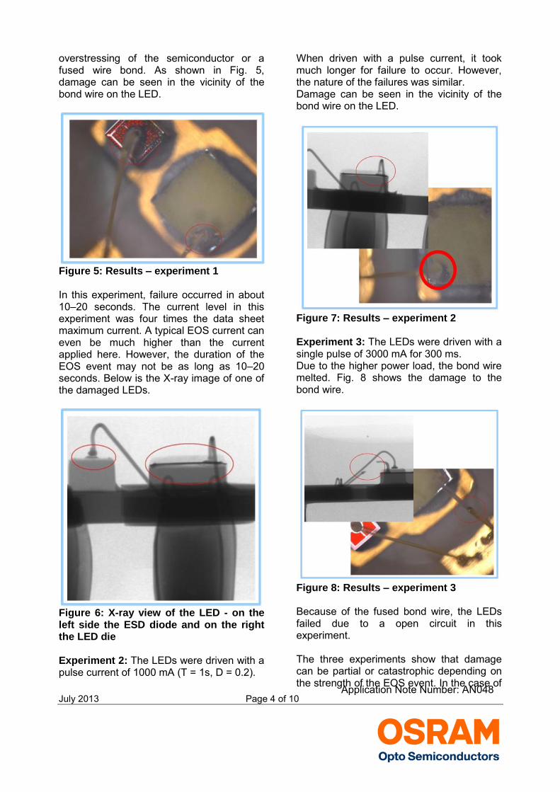
where an LED could be overdriven accidentally is if the driver cannot properly regulate the output current. For example, if the operating current of an LED circuit or system is extremely close to the maximum data sheet current, the driver should be able to tightly maintain the operating current. A inadequate designed driver which allows significant output current fluctuations can easily cause the maximum data sheet current to be exceeded, which in turn results in the overdriving of the LED. Some other sources outside the scope of this application note should be mentioned here for reference purposes only. Events such as power surges and lightning can also cause damage to LED circuits and systems if there are no external protection circuits to protect against these events. What type of damage can be expected as a result of EOS in LEDs? EOS damage in LEDs can be catastrophic in that the LED is permanently non-functional immediately after the EOS event; alternatively there may be just partial damage whereby a significant degradation in performance or the complete failure of the LED only occurs later on. Partial EOS damage in LEDs might manifest itself as reduced light output, poor thermal performance, and/or a shorter service life. Some of the EOS damage is visible using a microscope (or can even be spotted with the naked eye), but other types of damage require indirect testing, especially in the case of a single ESD-type event (e.g. I-V curve tracer, X-ray, SEM, etc.). The indirect way of testing for EOS damage involves biasing the LED and using a curve tracer to plot the current-voltage (I-V) curve characteristic of the damaged LED. The type of damage is highly dependent on the severity of the event. It can range from a burned LED die to molten or broken bond wire, a shorted LED, inhomogeneous appearance when lit, and hot spots. There may even be no obvious damage. For
reference purposes, some types of EOS damage are depicted in Fig. 4.
Figure 4: Visible and invisible LED damage caused by EOS It is also important to note that many EOS events do not damage the LED immediately. As a result, by the time LED failure occurs it may no longer be possible to associate the failure with the initial EOS event – even though the root cause of the failure may have been a single EOS experienced by the LED some while ago. What this means is that an EOS event can be easily overlooked by the time LED failure becomes obvious. This is yet another reason to strive to avoid EOS in LED circuits and systems. To illustrate the potential severity of EOS damage, some experiments were performed in the lab with known EOS events. Below are the results of known EOS events applied to an LED with the following data sheet maximum electrical rated values.
Experiment 1: LEDs were overdriven with a constant current of 1000 mA. The LEDs short-circuited fairly quickly. Possible failures here include the thermal
Application Note Number: AN048
July 2013 Page 4 of 10
overstressing of the semiconductor or a fused wire bond. As shown in Fig. 5, damage can be seen in the vicinity of the bond wire on the LED.
Figure 5: Results – experiment 1 In this experiment, failure occurred in about 10–20 seconds. The current level in this experiment was four times the data sheet maximum current. A typical EOS current can even be much higher than the current applied here. However, the duration of the EOS event may not be as long as 10–20 seconds. Below is the X-ray image of one of the damaged LEDs.
Figure 6: X-ray view of the LED - on the left side the ESD diode and on the right the LED die Experiment 2: The LEDs were driven with a pulse current of 1000 mA (T = 1s, D = 0.2).
When driven with a pulse current, it took much longer for failure to occur. However, the nature of the failures was similar. Damage can be seen in the vicinity of the bond wire on the LED.
Figure 7: Results – experiment 2 Experiment 3: The LEDs were driven with a single pulse of 3000 mA for 300 ms. Due to the higher power load, the bond wire melted. Fig. 8 shows the damage to the bond wire.
Figure 8: Results – experiment 3 Because of the fused bond wire, the LEDs failed due to a open circuit in this experiment. The three experiments show that damage can be partial or catastrophic depending on the strength of the EOS event. In the case of Application Note Number: AN048
July 2013 Page 5 of 10
partial damage, multiple EOS events are required before complete failure occurs. How to protect LEDs from EOS Since the ultimate result of an EOS event is overcurrent or overvoltage there are two types of protection that are commonly used in the industry:
1. Overvoltage protection devices 2. Current limiters
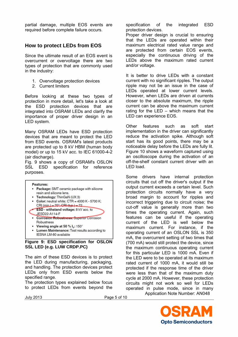
Before looking at these two types of protection in more detail, let's take a look at the ESD protection devices that are integrated into OSRAM LEDs and clarify the importance of proper driver design in an LED system. Many OSRAM LEDs have ESD protection devices that are meant to protect the LED from ESD events. OSRAM's latest products are protected up to 8 kV HBM (human body model) or up to 15 kV acc. to IEC 61000-4-2 (air discharge). Fig. 9 shows a copy of OSRAM's OSLON SSL ESD specification for reference purposes.
Figure 9: ESD specification for OSLON SSL LED (e.g. LUW CRDP.PC) The aim of these ESD devices is to protect the LED during manufacturing, packaging, and handling. The protection devices protect LEDs only from ESD events below the specified range. The protection types explained below focus to protect LEDs from events beyond the
specification of the integrated ESD protection devices. Proper driver design is crucial to ensuring that the LEDs are operated within their maximum electrical rated value range and are protected from certain EOS events, especially the continuous driving of the LEDs above the maximum rated current and/or voltage. It is better to drive LEDs with a constant current with no significant ripples. The output ripple may not be an issue in the case of LEDs operated at lower current levels. However, when LEDs are driven at currents closer to the absolute maximum, the ripple current can be above the maximum current rating for the LED – which means that the LED can experience EOS. Other features such as soft start implementation in the driver can significantly reduce the activation spike. Although soft start has its good points, there may be a noticeable delay before the LEDs are fully lit. Figure 10 shows a waveform captured using an oscilloscope during the activation of an off-the-shelf constant current driver with an LED load. Some drivers have internal protection circuits that cut off the driver's output if the output current exceeds a certain level. Such protection circuits normally have a very broad margin to account for ripples and incorrect triggering due to circuit noise; the cut-off value is generally more than two times the operating current. Again, such features can be useful if the operating current of the LED is well below the maximum current. For instance, if the operating current of an OSLON SSL is 350 mA, the overcurrent setting of two times that (700 mA) would still protect the device, since the maximum continuous operating current for this particular LED is 1000 mA. Even if the LED were to be operated at its maximum rated current of 1000 mA, it would still be protected if the response time of the driver were less than that of the maximum duty cycle at 2000 mA. However, these protection circuits might not work so well for LEDs operated in pulse mode, since in many
Application Note Number: AN048
July 2013 Page 6 of 10
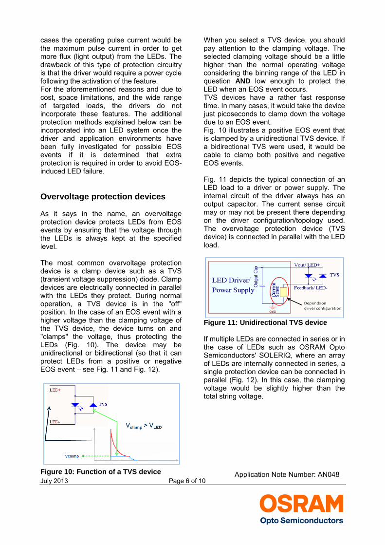
cases the operating pulse current would be the maximum pulse current in order to get more flux (light output) from the LEDs. The drawback of this type of protection circuitry is that the driver would require a power cycle following the activation of the feature. For the aforementioned reasons and due to cost, space limitations, and the wide range of targeted loads, the drivers do not incorporate these features. The additional protection methods explained below can be incorporated into an LED system once the driver and application environments have been fully investigated for possible EOS events if it is determined that extra protection is required in order to avoid EOS-induced LED failure. Overvoltage protection devices As it says in the name, an overvoltage protection device protects LEDs from EOS events by ensuring that the voltage through the LEDs is always kept at the specified level. The most common overvoltage protection device is a clamp device such as a TVS (transient voltage suppression) diode. Clamp devices are electrically connected in parallel with the LEDs they protect. During normal operation, a TVS device is in the "off" position. In the case of an EOS event with a higher voltage than the clamping voltage of the TVS device, the device turns on and "clamps" the voltage, thus protecting the LEDs (Fig. 10). The device may be unidirectional or bidirectional (so that it can protect LEDs from a positive or negative EOS event – see Fig. 11 and Fig. 12).
Figure 10: Function of a TVS device
When you select a TVS device, you should pay attention to the clamping voltage. The selected clamping voltage should be a little higher than the normal operating voltage considering the binning range of the LED in question AND low enough to protect the LED when an EOS event occurs. TVS devices have a rather fast response time. In many cases, it would take the device just picoseconds to clamp down the voltage due to an EOS event. Fig. 10 illustrates a positive EOS event that is clamped by a unidirectional TVS device. If a bidirectional TVS were used, it would be cable to clamp both positive and negative EOS events. Fig. 11 depicts the typical connection of an LED load to a driver or power supply. The internal circuit of the driver always has an output capacitor. The current sense circuit may or may not be present there depending on the driver configuration/topology used. The overvoltage protection device (TVS device) is connected in parallel with the LED load.
Figure 11: Unidirectional TVS device If multiple LEDs are connected in series or in the case of LEDs such as OSRAM Opto Semiconductors' SOLERIQ, where an array of LEDs are internally connected in series, a single protection device can be connected in parallel (Fig. 12). In this case, the clamping voltage would be slightly higher than the total string voltage.
Application Note Number: AN048
July 2013 Page 7 of 10
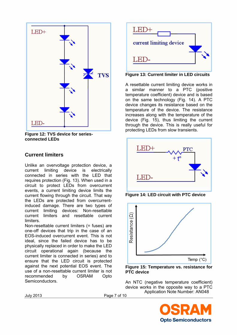
Figure 12: TVS device for series-connected LEDs Current limiters Unlike an overvoltage protection device, a current limiting device is electrically connected in series with the LED that requires protection (Fig. 13). When used in a circuit to protect LEDs from overcurrent events, a current limiting device limits the current flowing through the circuit. That way the LEDs are protected from overcurrent-induced damage. There are two types of current limiting devices: Non-resettable current limiters and resettable current limiters. Non-resettable current limiters (= fuses) are one-off devices that trip in the case of an EOS-induced overcurrent event. This is not ideal, since the failed device has to be physically replaced in order to make the LED circuit operational again (because the current limiter is connected in series) and to ensure that the LED circuit is protected against the next potential EOS event. The use of a non-resettable current limiter is not recommended by OSRAM Opto Semiconductors.
Figure 13: Current limiter in LED circuits A resettable current limiting device works in a similar manner to a PTC (positive temperature coefficient) device and is based on the same technology (Fig. 14). A PTC device changes its resistance based on the temperature of the device. The resistance increases along with the temperature of the device (Fig. 15), thus limiting the current through the device. This is really useful for protecting LEDs from slow transients.
Figure 14: LED circuit with PTC device
Figure 15: Temperature vs. resistance for PTC device An NTC (negative temperature coefficient) device works in the opposite way to a PTC
Application Note Number: AN048
July 2013 Page 8 of 10
device. It has a higher resistance at room temperature and a negligible resistance at operating temperature, which makes it ideal for protecting against inrush current. Fig. 16 illustrates how an NTC protects against inrush current as a result of hot plugging.
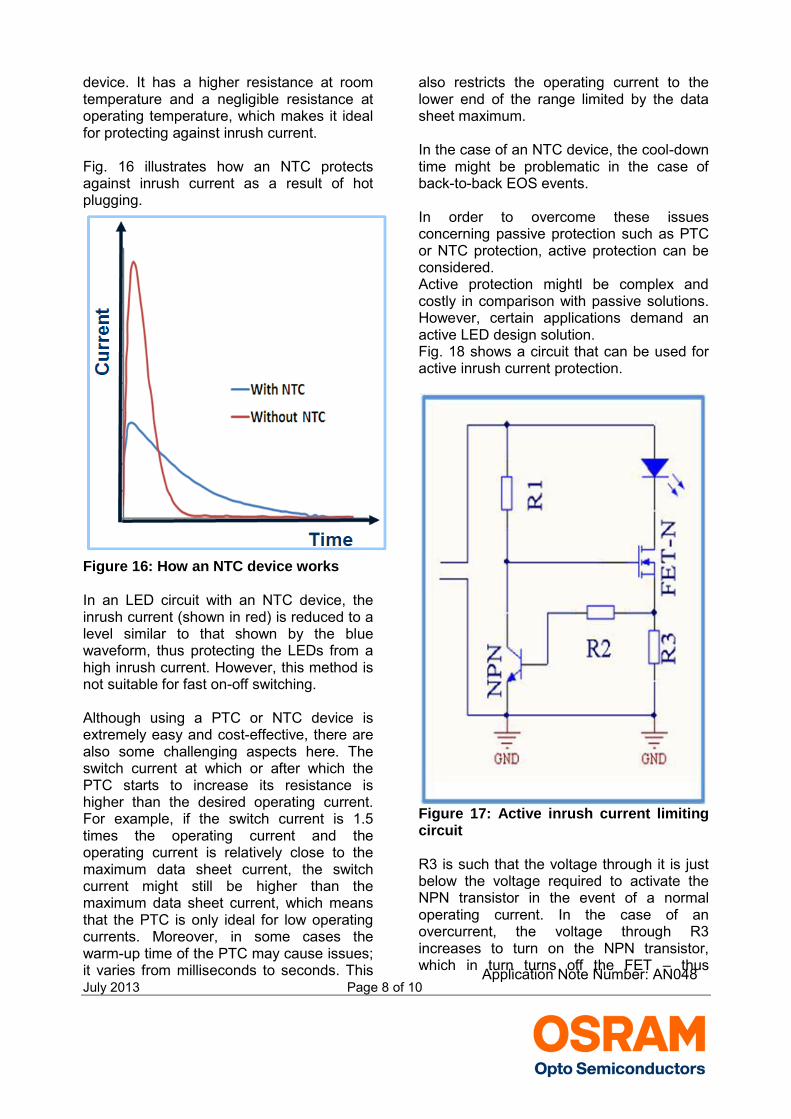
Figure 16: How an NTC device works In an LED circuit with an NTC device, the inrush current (shown in red) is reduced to a level similar to that shown by the blue waveform, thus protecting the LEDs from a high inrush current. However, this method is not suitable for fast on-off switching. Although using a PTC or NTC device is extremely easy and cost-effective, there are also some challenging aspects here. The switch current at which or after which the PTC starts to increase its resistance is higher than the desired operating current. For example, if the switch current is 1.5 times the operating current and the operating current is relatively close to the maximum data sheet current, the switch current might still be higher than the maximum data sheet current, which means that the PTC is only ideal for low operating currents. Moreover, in some cases the warm-up time of the PTC may cause issues; it varies from milliseconds to seconds. This
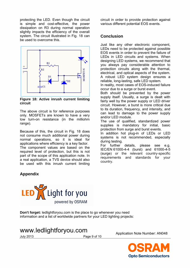
also restricts the operating current to the lower end of the range limited by the data sheet maximum. In the case of an NTC device, the cool-down time might be problematic in the case of back-to-back EOS events. In order to overcome these issues concerning passive protection such as PTC or NTC protection, active protection can be considered. Active protection mightl be complex and costly in comparison with passive solutions. However, certain applications demand an active LED design solution. Fig. 18 shows a circuit that can be used for active inrush current protection.
Figure 17: Active inrush current limiting circuit R3 is such that the voltage through it is just below the voltage required to activate the NPN transistor in the event of a normal operating current. In the case of an overcurrent, the voltage through R3 increases to turn on the NPN transistor, which in turn turns off the FET – thus Application Note Number: AN048
July 2013 Page 9 of 10
protecting the LED. Even though the circuit is simple and cost-effective, the power dissipation on R3 during normal operation slightly impacts the efficiency of the overall system. The circuit illustrated in Fig. 18 can be used to overcome this.
Figure 18: Active inrush current limiting circuit The above circuit is for reference purposes only. MOSFETs are known to have a very low turn-on resistance (in the milliohm range). Because of this, the circuit in Fig. 18 does not consume much additional power during normal operations, so it is ideal for applications where efficiency is a key factor. The component values are based on the required level of protection, but this is not part of the scope of this application note. In a real application, a TVS device should also be used with this inrush current limiting
circuit in order to provide protection against various different potential EOS events. Conclusion Just like any other electronic component, LEDs need to be protected against possible EOS events in order to prevent the failure of LEDs in LED circuits and systems. When designing LED systems, we recommend that you always pay considerable attention to protection circuits along with the thermal, electrical, and optical aspects of the system. A robust LED system design ensures a reliable, long-lasting, safe LED system. In reality, most cases of EOS-induced failure occur due to a surge or burst event. Both should be prevented by the power supply itself. Usually, a surge is dealt with fairly well by the power supply or LED driver circuit. However, a burst is more critical due to its duration, frequency, and intensity, and can lead to damage to the power supply and/or LED module. The use of qualified, standardized power supplies is mandatory for initial, basic protection from surge and burst events. In addition hot plug-in of LEDs or LED systems is not recommended, especially during testing. For further details, please see e.g. IEC/EN 61000-4-4 (burst) and 61000-4-5 (surge) or the relevant country-specific requirements and standards for your country.
Appendix
Don't forget: ledlightforyou.com is the place to go whenever you need information and a list of worldwide partners for your LED lighting projects:
www.ledlightforyou.com Application Note Number: AN048
July 2013 Page 10 of 10
Authors: Muhinthan Murugesu, Horst Varga, Norbert Häfner, Andreas Stich, Christine Rafael ABOUT OSRAM OPTO SEMICONDUCTORS OSRAM, Munich, Germany is one of the two leading light manufacturers in the world. Its subsidiary, OSRAM Opto Semiconductors GmbH in Regensburg (Germany), offers its customers solutions based on semiconductor technology for lighting, sensor and visualization applications. Osram Opto Semiconductors has production sites in Regensburg (Germany), Penang (Malaysia) and Wuxi (China). Its headquarters for North America is in Sunnyvale (USA), and for Asia in Hong Kong. Osram Opto Semiconductors also has sales offices throughout the world. For more information go to www.osram-os.com. DISCLAIMER PLEASE CAREFULLY READ THE BELOW TERMS AND CONDITIONS BEFORE USING THE INFORMATION SHOWN HEREIN. IF YOU DO NOT AGREE WITH ANY OF THESE TERMS AND CONDITIONS, DO NOT USE THE INFORMATION. The information shown in this document is provided by OSRAM Opto Semiconductors GmbH on an “as is basis” and without OSRAM Opto Semiconductors GmbH assuming, express or implied, any warranty or liability whatsoever, including, but not limited to the warranties of correctness, completeness, merchantability, fitness for a particular purpose, title or non-infringement of rights. In no event shall OSRAM Opto Semiconductors GmbH be liable - regardless of the legal theory - for any direct, indirect, special, incidental, exemplary, consequential, or punitive damages related to the use of the information. This limitation shall apply even if OSRAM Opto Semiconductors GmbH has been advised of possible damages. As some jurisdictions do not allow the exclusion of certain warranties or limitations of liability, the above limitations or exclusions might not apply. The liability of OSRAM Opto Semiconductors GmbH would in such case be limited to the greatest extent permitted by law. OSRAM Opto Semiconductors GmbH may change the information shown herein at anytime without notice to users and is not obligated to provide any maintenance (including updates or notifications upon changes) or support related to the information. Any rights not expressly granted herein are reserved. Except for the right to use the information shown herein, no other rights are granted nor shall any obligation be implied requiring the grant of further rights. Any and all rights or licenses for or regarding patents or patent applications are expressly excluded.
Application Note Number: AN048