Embed Size (px)
Citation preview
1
Accelerated Aging with Electrical Overstress andPrognostics for Power MOSFETs
Sankalita Saha, Member, IEEE, Jose. R. Celaya, Member, IEEE, Vladislav Vashchenko, Shompa Mahiuddin,and Kai. F. Goebel.
Abstract—Power electronics play an increasingly importantrole in energy applications as part of their power convertercircuits. Understanding the behavior of these devices, especiallytheir failure modes as they age with nominal usage or suddenfault development is critical in ensuring efficiency. In this paper,a prognostics based health management of power MOSFETsundergoing accelerated aging through electrical overstress atthe gate area is presented. Details of the accelerated agingmethodology, modeling of the degradation process of the deviceand prognostics algorithm for prediction of the future state ofhealth of the device are presented. Experiments with multipledevices demonstrate the performance of the model and theprognostics algorithm as well as the scope of application.
Index Terms—Power MOSFET, accelerated aging, prognostics.
I. INTRODUCTION
POWER electronic devices have become a crucial compo-nent in most modern energy systems varying from wind
turbines to hybrid electric cars as they are integral to powerconverter circuits. Leading research efforts related to thesedevices are focused on new device designs for performanceoptimizations and cost reduction. However, understanding thebehavior of these devices as they undergo regular wear and tearduring their lifetimes or unexpected operational conditions isequally important, if not more, for ensuring operational safetyand preventing unexpected failures. In particular, for applica-tions where remote deployment is used such as off-shore wind-turbines, a clear understanding of the failure modes of thesedevices and corresponding health management techniques isrequired to ensure both performance and cost-effectiveness.
Degradation in the characteristic performance of the devicecan happen not only when they are subjected to operatingconditions beyond their specifications but also due to regularusage and storage over time. Currently, most of the healthmanagement of the devices is based on reliability basedmaintenance [1]. However, in many cases, this is neithersufficient nor efficient. Each of these devices can go throughvery different life-cycles and hence different aging. Hence, ifmaintenance is done based purely on reliability analysis, inmost cases the devices will either be discarded before they
Sankalita Saha is with MCT/NASA Ames Research Center, Moffett Field,94035, USA e-mail:[email protected].
Jose. R. Celaya is with SGT/NASA Ames Research Center, Moffett Field,94035, USA.
Vladislav Vashchenko was with National Semiconductor Corp.Shompa Mahiuddin was an intern at NASA Ames Research Center, Moffett
Field, 94035, USA.Kai. F. Goebel is with NASA Ames Research Center, Moffett Field, 94035,
USA.
have reached their end of life (EoL) or worse, fail before theirscheduled replacement. Given the criticality of the systems inwhich these devices are used, a more customized approach forindividual devices based on the application profile and usagemonitoring is required.
This paper presents such a customized approach for apower MOSFET (Metal Oxide Semiconductor Field EffectTransistor). The approach is based on prognostics based healthmanagement techniques used traditionally in mechanical sys-tems. These techniques involve periodic monitoring in orderto assess the remaining life of a degraded or aged systemfollowed by making a prediction of the time of failure underanticipated future loading and operational conditions. Theaging mechanism is emulated with an accelerated aging testprocedure. Accelerated aging tests (ALTs) or highly accel-erated aging tests (HALTs) are used very commonly in thereliability domain and the semiconductor industry to estimatethe expected lifetimes of the device as well as limits on operat-ing conditions [2]. However, the accelerated tests used for theexperiments in prognostic health management are somewhatdifferent as explained in later sections. The accelerated testsused in this paper target a particularly weak region in thepower MOSFET – the gate interface – which is susceptible todamage from high voltage [3]. The results from the acceleratedaging tests are analyzed to first identify a precursor of damageand then make estimates of the remaining useful life (RUL) fora given device based on the precursor trend. RUL estimatescan then be used to make decisions for maintenance of thedevice as well as the enclosing sub-system.
Currently, most ALTs and HALTs for power electronics inthe reliability domain focus on thermal stress either throughtemperature or power cycling [4] and mechanical stress [5].Within the prognostics domain, the work done so far hasmainly looked into electro-thermal cycling induced thermalfatigue ([6], [7] and [8]). However, purely electrical stressrelated failures are quite common to power MOSFETs as theyare prone to damage from radiation, electro-static discharge(ESD) and lightning surges. A significant body of work hasfocused on radiation related faults [9] while recently, somework on analyzing the effects of ESD [10] and lightningsurges [11] on power electronics have been reported. Exploringthe effects of hot-carrier effects in MOSFETs have receivedconsiderable attention as well ([3], [12]). However, most ofthe work is not oriented toward prognostics and is limitedto developing testbeds to trigger and study the phenomenon.To the best of our knowledge, this work represents the firstattempt at developing a prognostic technique for electricalstress on power MOSFETs.
https://ntrs.nasa.gov/search.jsp?R=20110014343 2018-12-24T16:45:34+00:00Z
2
II. BACKGROUND
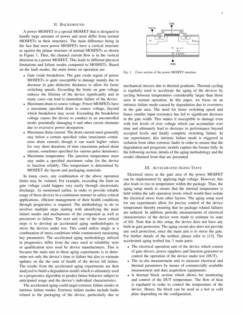
A power MOSFET is a special MOSFET that is designed tohandle large amounts of power and most differ from normalMOSFETs in their structures. The main difference being inthe fact that most power MOSFETs have a vertical structureas against the planar structure of normal MOSFETs as shownin Figure 1. Thus, the channel current flow is in the verticaldirection in a power MOSFET. This leads to different physicallimitations and failure modes compared to MOSFETs. Basedon the fault modes, the main limits on operation are:
• Gate oxide breakdown: The gate oxide region of powerMOSFETs is quite susceptible to damage mainly due todecrease in gate dielectric thickness to allow for fasterswitching speeds. Exceeding the limits on gate voltagereduces the lifetime of the device significantly and inmany cases can lead to immediate failure of the device.
• Maximum drain to source voltage: Power MOSFETs havea maximum specified drain to source voltage, beyondwhich breakdown may occur. Exceeding the breakdownvoltage causes the device to conduct in an uncontrolledmode, potentially damaging it and other circuit elementsdue to excessive power dissipation.
• Maximum drain current: The drain current must generallystay below a certain specified value (maximum contin-uous drain current) though it can reach higher valuesfor very short durations of time (maximum pulsed draincurrent, sometimes specified for various pulse durations).
• Maximum temperature: The junction temperature muststay under a specified maximum value for the deviceto function reliably. This temperature is determined byMOSFET die layout and packaging materials.
In many cases, any combination of the above operationlimits may be violated. For example, exceeding the limit ongate voltage could happen very easily through electrostaticdischarge. As mentioned earlier, in order to provide reliableusage of these devices in a continuous manner in safety-criticalapplications, efficient management of their health conditionsthrough prognostics is required. The methodology to do soinvolves multiple steps starting with identifying the mainfailure modes and mechanisms of the component as well asprecursors to failure. The next and one of the most criticalsteps is to develop an accelerated aging methodologies tostress the devices under test. This could utilize single or acombination of stress conditions while continuously measuringkey parameters. The accelerated aging methodology utilizedin prognostics differ from the ones used in reliability testsor qualification tests used by device manufacturers. This isbecause the main aim in these aging experiments is to deter-mine not only the device’s time to failure but also to estimateupdates on the the state of health of the device till failure.The results from the accelerated aging experiments are thenanalyzed to build a degradation model which is ultimately usedin a prognostics algorithm to predict future behavior subject toanticipated usage and the device’s individual characteristics.
The accelerated aging could target extrinsic failure modes orintrinsic failure modes. Extrinsic failure modes include faultsrelated to the packaging of the device, particularly due to
Fig. 1. Cross section of the power MOSFET structure.
mechanical stresses due to thermal gradients. Thermal cyclingis regularly used to accelerate the aging of the devices bycycling between temperatures considerably larger than thoseseen in normal operation. In this paper, we focus on anintrinsic failure mode caused by degradation due to overstressin the gate area. The need for faster switching speed andhence smaller input resistance has led to significant decreasein the gate width. This makes it susceptible to damage evenwith low levels of over voltage which can accumulate overtime and ultimately lead to decrease in performance beyondaccepted levels and finally complete switching failure. Inour experiments, this intrinsic failure mode is triggered inisolation from other extrinsic faults in order to ensure that thedegradation and prognostic models capture the former fully. Inthe following section, details of the aging methodology and theresults obtained from that are presented.
III. ACCELERATED AGING TESTS
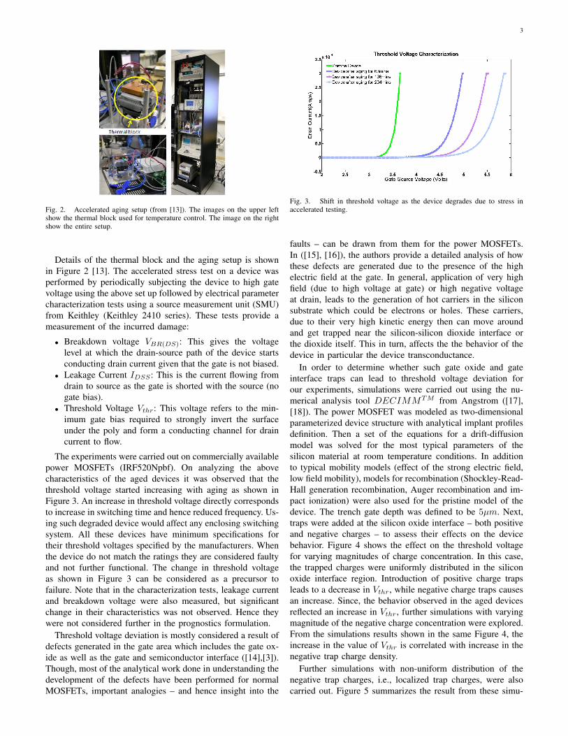
Electrical stress at the gate area of the power MOSFETcan be implemented by applying high voltage. However, thisalso leads to rise in temperature within the package. Thus, theaging setup needs to ensure that the internal temperature isheld within the safe operation levels which would then isolatethe electrical stress from other factors. The aging setup usedfor our experiments allow for precise control of the devicetemperature thereby ensuring that no package related failuresare induced. In addition, periodic measurements of electricalcharacteristics of the device were made to estimate its stateof life. Note that in this setup, the device does not have anybuilt-in gate protection. The aging circuit also does not provideany such protection, since the main aim is to stress the gate.For further details of the testbed, please refer to [13]. Theaccelerated aging testbed has 3 main parts:
• The electrical operation unit of the device which consistof gate drivers, power suppliers and function generator tocontrol the operation of the device under test (DUT).
• The in-situ measurement unit to measure electrical andthermal parameters by means of commercially availablemeasurement and data acquisition equipments.
• A thermal block section which allows for monitoringand control of the DUT temperature. The flow of heatis regulated in order to control the temperature of thedevice. Hence, the block can be used as a hot or coldplate depending on the configuration.
3
Fig. 2. Accelerated aging setup (from [13]). The images on the upper leftshow the thermal block used for temperature control. The image on the rightshow the entire setup.
Details of the thermal block and the aging setup is shownin Figure 2 [13]. The accelerated stress test on a device wasperformed by periodically subjecting the device to high gatevoltage using the above set up followed by electrical parametercharacterization tests using a source measurement unit (SMU)from Keithley (Keithley 2410 series). These tests provide ameasurement of the incurred damage:
• Breakdown voltage VBR(DS): This gives the voltagelevel at which the drain-source path of the device startsconducting drain current given that the gate is not biased.
• Leakage Current IDSS : This is the current flowing fromdrain to source as the gate is shorted with the source (nogate bias).
• Threshold Voltage Vthr: This voltage refers to the min-imum gate bias required to strongly invert the surfaceunder the poly and form a conducting channel for draincurrent to flow.
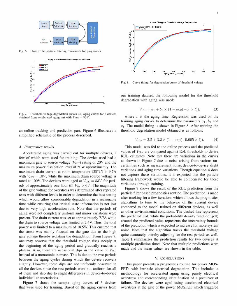
The experiments were carried out on commercially availablepower MOSFETs (IRF520Npbf). On analyzing the abovecharacteristics of the aged devices it was observed that thethreshold voltage started increasing with aging as shown inFigure 3. An increase in threshold voltage directly correspondsto increase in switching time and hence reduced frequency. Us-ing such degraded device would affect any enclosing switchingsystem. All these devices have minimum specifications fortheir threshold voltages specified by the manufacturers. Whenthe device do not match the ratings they are considered faultyand not further functional. The change in threshold voltageas shown in Figure 3 can be considered as a precursor tofailure. Note that in the characterization tests, leakage currentand breakdown voltage were also measured, but significantchange in their characteristics was not observed. Hence theywere not considered further in the prognostics formulation.
Threshold voltage deviation is mostly considered a result ofdefects generated in the gate area which includes the gate ox-ide as well as the gate and semiconductor interface ([14],[3]).Though, most of the analytical work done in understanding thedevelopment of the defects have been performed for normalMOSFETs, important analogies – and hence insight into the
Fig. 3. Shift in threshold voltage as the device degrades due to stress inaccelerated testing.
faults – can be drawn from them for the power MOSFETs.In ([15], [16]), the authors provide a detailed analysis of howthese defects are generated due to the presence of the highelectric field at the gate. In general, application of very highfield (due to high voltage at gate) or high negative voltageat drain, leads to the generation of hot carriers in the siliconsubstrate which could be electrons or holes. These carriers,due to their very high kinetic energy then can move aroundand get trapped near the silicon-silicon dioxide interface orthe dioxide itself. This in turn, affects the the behavior of thedevice in particular the device transconductance.
In order to determine whether such gate oxide and gateinterface traps can lead to threshold voltage deviation forour experiments, simulations were carried out using the nu-merical analysis tool DECIMMTM from Angstrom ([17],[18]). The power MOSFET was modeled as two-dimensionalparameterized device structure with analytical implant profilesdefinition. Then a set of the equations for a drift-diffusionmodel was solved for the most typical parameters of thesilicon material at room temperature conditions. In additionto typical mobility models (effect of the strong electric field,low field mobility), models for recombination (Shockley-Read-Hall generation recombination, Auger recombination and im-pact ionization) were also used for the pristine model of thedevice. The trench gate depth was defined to be 5µm. Next,traps were added at the silicon oxide interface – both positiveand negative charges – to assess their effects on the devicebehavior. Figure 4 shows the effect on the threshold voltagefor varying magnitudes of charge concentration. In this case,the trapped charges were uniformly distributed in the siliconoxide interface region. Introduction of positive charge trapsleads to a decrease in Vthr, while negative charge traps causesan increase. Since, the behavior observed in the aged devicesreflected an increase in Vthr, further simulations with varyingmagnitude of the negative charge concentration were explored.From the simulations results shown in the same Figure 4, theincrease in the value of Vthr is correlated with increase in thenegative trap charge density.
Further simulations with non-uniform distribution of thenegative trap charges, i.e., localized trap charges, were alsocarried out. Figure 5 summarizes the result from these simu-

4
Fig. 4. Shift in threshold voltage with varying density of positive and negativetrap charges. The charge distribution is uniform.
Fig. 5. Shift in threshold voltage with localized negative trap charges. Thecharge concentration is 1e12C − cm−2.
lations. The symbol Y in Figure 5 refers to the depth in µm asmeasured from the gate towards the drain. Thus, 5 < Y < 6implies the region between 5µm and 6µm below the silicon-silicon dioxide interface. Y = 0 refers to the start of theinterface. Thus, the nearer to the interface the local trappedcharges, the more the threshold voltage increases.
After determining the precursor to failure, the next step isto determine the EoL criteria based on the precursor trend.In this case, the EoL is determined by when these deviceswill be rendered non-functional. Though a complete failuremay imply that the device stops switching completely, in mostapplications deviation beyond manufacturer’s ratings can beconsidered failures. Unfortunately, there are no guidelines onwhat constitutes their failure since these devices are used ina wide variety of applications; each application is expected tohave different failure criteria based on the enclosing system’stolerance for switching delays and errors. For the device usedin our experiments, the threshold voltage for a functionaldevice is expected to vary from a minimum of 3V to amaximum of 4V. We set the failure criteria to be when thethreshold voltage increases to more than an increase of 50%at 6.1V. Thus, EoL is reached by a device when its thresholdvoltage attains 6.1V. In the next section, we develop a modelthat captures this shift in threshold voltage with aging cyclesand combine it with a prognostic algorithm to predict the RULfor the aged devices.
IV. MODELING
Prognostics algorithms can be based on model-based tech-niques relying on a detailed degradation model of the unit,data-driven techniques where prediction models are createdbased on learning from past history or hybrid where a simplermodel is used in conjunction with a data-driven algorithm.The hybrid methods have several advantages; the simplicityof the model makes it easier to implement especially forapplications where computational resources may be scarce,while at the same time the support of data-driven methodsallows to compensate for the simplicity of the model andcapture complex or unmodeled behavior. In this work, a hybridapproach was used. The prognostics algorithm involves twosteps; first the simple aging model is built offline based ontraining data sets which provide insights regarding the physicalbehavior of th degradation. Next, in online mode, the model isfit into a prediction algorithm – particle filters (PF) in our work– which tracks the behavior of the system for further tuningand then starts making predictions of the RUL. Typically, theprediction routine is triggered by a diagnostic flag and eithercontinuous prediction of the state of health and RUL predictionis made or discrete time predictions are made which can thenbe used to make health management decisions.
Particle filtering is a sequential Monte Carlo (SMC) tech-nique for implementing a recursive Bayesian filter using MonteCarlo simulations. It is primarily used for state estimationand tracking. The mathematical formulation for PF methodshave been discussed in [19]. The basic idea is to develop anonparametric representation of the system state probabilitydensity function (pdf) in the form of a set of particles withassociated importance weights. The particles are sampledvalues from the unknown state space and the weights arethe corresponding discrete probability masses. As the filteriterates, the particles are propagated according to the systemstate transition model, while their weights are updated basedupon the likelihood of the measurement given the particlevalues. Resampling of the particle distribution is done whenneeded in order to prevent the degeneracy of the weights.Particle filters can be represented mathematically as follows:
xk = f(xk−1) + ωk, (1)
yk = h(xk) + νk, (2)
where k is the time index, x denotes the state, y is theoutput or measurements. Both ω and ν are samples fromnoise distributions which are picked from zero mean Gaussiandistributions whose standard deviations are derived from thegiven training data, thus accommodating for the sources ofuncertainty in feature extraction, regression modeling andmeasurement.
For state prediction purposes the same PF framework canbe used by running only the state equation-based particlepropagation step until the predicted state value crosses somepredetermined EoL threshold. The predicted trajectory of eachparticle then generates an estimate of RUL, which can becombined with the associated weights to give the RUL pdf.The process is broken down into an offline learning part, and
5
Fig. 6. Flow of the particle filtering framework for prognostics
Fig. 7. Threshold voltage degradation curves i.e., aging curves for 3 devicesobtained from accelerated aging test with VGS = 53V .
an online tracking and prediction part. Figure 6 illustrates asimplified schematic of the process described.
A. Prognostics results
Accelerated aging was carried out for multiple devices, afew of which were used for training. The device used had amaximum gate to source voltage (VGS) rating of 20V and themaximum power dissipation level of 50W approximately. Themaximum drain current at room temperature (25◦C) is 9.7Awith VGS = 10V , while the maximum drain source voltage israted at 100V. The devices were aged at VGS = 53V for peri-ods of approximately one hour till Vth > 6V . The magnitudeof the gate voltage for overstress was determined after repeatedtests with different levels in order to determine the best settingwhich would allow considerable degradation in a reasonabletime while ensuring that critical state information is not lostdue to very high acceleration rate. Note that the periods ofaging were not completely uniform and minor variations werepresent. The drain current was set at approximately 7.7A whilethe drain to source voltage was limited at 2.4V. Thus, the totalpower was limited to a maximum of 18.5W. This ensured thatthe stress was mainly focused on the gate due to the highgate voltage thereby isolating the degradation. From Figure 7,one may observe that the threshold voltage rises steeply atthe beginning of the aging period and gradually reaches aplateau. Also, there are occasional dips in the value of Vthrinstead of a monotonic increase. This is due to the rest periodsbetween the aging cycles during which the device recoversslightly. However, these dips are not uniformly observed inall the devices since the rest periods were not uniform for allof them and also due to slight differences in device-to-deviceindividual characteristics.
Figure 7 shows the sample aging curves of 3 devicesthat were used for training. Based on the aging curves from
Fig. 8. Curve fitting for degradation curve of threshold voltage
our training dataset, the following model for the thresholddegradation with aging was used:
Vthr = a1 + b1 × (1− exp(−c1 × t)), (3)
where t is the aging time. Regression was used on thetraining aging curves to determine the parameters a1, b1 andc1. The model fitting is shown in Figure 8. After training thethreshold degradation model obtained is as follows:
Vthr = 3.5 + 3.2× (1− exp(−0.005× t)). (4)
This model was fed to the online process and the predictedvalues of Vthr are compared against EoL thresholds to deriveRUL estimates. Note that there are variations in the curvesas shown in Figure 7 due to noise arising from various un-certainties such as measurement noise, device-to-device slightvariations and aging time variations. Though equation 4 doesnot capture these variations, it is expected that the particlefiltering framework would be able to compensate for thesevariations through training.
Figure 9 shows the result of the RUL prediction from theparticle filter based prognostics routine. The prediction is madeafter tracking for a few iterations which allows the prognosticsalgorithms to tune to the behavior of the current devicecompared to the model trained on different devices, as wellas other environmental conditions. The dashed line representsthe predicted EoL while the probability density function (pdf)around the predicted value represents the uncertainty boundsof the prediction which is expected to increase for more systemnoise. Note that the algorithm tracks the threshold voltagequite accurately, thereby adjusting for the rest periods as well.Table I summarizes the prediction results for two devices atmultiple prediction times. Note that multiple predictions weremade and the mean values are shown in the table.
V. CONCLUSIONS
This paper presents a prognostics routine for power MOS-FETs with intrinsic electrical degradation. This included amethodology for accelerated aging using purely electricaloverstress and corresponding identification of a precursor offailure. The devices were aged using accelerated electricaloverstress at the gate of the power MOSFET which triggered

6
Fig. 9. Particle filter based tracking and prediction of threshold voltagedegradation and EoL of device
TABLE IRUL PREDICTION RESULTS
Device Time of Predicted Actualid prediction(mins) RUL(mins) RUL(mins)
Device1 248 172 192Device1 312 118.85 128Device2 263 136.5 191Device2 330 98 114
degradation in the threshold voltage of the device due tointerface trap charge accumulation. Model for the degradationcurves were derived and used in particle filtering framework topredict RUL estimates. The prognostics routine was robust andcould handle system noise factors such as uneven rest periodsbetween aging. Since the prognostics algorithm provides aRUL pdf, instead of a single value, the interpretation of theprognostic result is useful and intuitive. Future work includesrefinement of the model and applying it to a larger trainingas well as test data set generation. Tighter integration of thethe aging setup with the SMU and/or identification of otherprecursors that can be easily integrated to enable completelyautomated aging is also an important future direction of work.
REFERENCES
[1] E. Suhir, How to Make a Device into a Product: Accelerated LifeTesting (ALT), Its Role, Attributes, Challenges, Pitfalls and Interactionwith Qualification Tests”, ser. Micro- and Opto-Electrtonic Materialsand Structures: Physics, Mechanics, Design, Reliability, Packaging.Springer, 2007, vol. 2.
[2] J.-M. Thebaud, E. Woirgard, C. Zardini, S. Azzopardi, O. Briat, and J.-M. Vinassa, “Strategy for designing accelerated aging tests to evaluateigbt power modules lifetime in real operation mode,” Components andPackaging Technologies, IEEE Transactions on, vol. 26, no. 2, pp. 429– 438, 2003.
[3] R. Marrakh and A. Bouhdada, “Modeling of interface defect distribu-tion for an n-mosfets under hot-carrier stressing,” Active and PassiveElectronic Components, vol. 23, 3, pp. 137–144, 2000.
[4] A. Morozumi, K. Yamada, T. Miyasaka, and Y. Seki, “Reliability ofpower cycling for igbt power semiconductor modules,” in Industry Appli-cations Conference, 2001. Thirty-Sixth IAS Annual Meeting. ConferenceRecord of the 2001 IEEE, 2001.
[5] P. Lall, C. Bhat, M. Hande, V. More, R. Vaidya, J. Suhling, R. Pandher,and K. Goebel, “Latent damage assessent and prognostication of residuallife in airborne lead-free electronics under thermo- mechanical loads,”in Proceedings of International Conference on Prognostics and HealthManagement, 2008.
[6] B. Saha, J. Celaya, K. Goebel, and P.Wysocki, “Towards prognostics forelectronics components,” in Proceedings of IEEE AEROSPACE, 2009.
[7] A. Ginart, M. Roemer, P. Kalgren, and K. Goebel, “Modeling aging ef-fects of igbts in power drives by ringing characterization,” in Prognosticsand Health Management, 2008. PHM 2008. International Conferenceon, 2008, pp. 1 –7.
[8] J. R. Celaya, N. Patil, S. Saha, P. Wysocki, and K. Goebel, “Towardsaccelerated aging methodlogies and health management of power mos-fets (technical brief),” in Proceedings of Annual Conference of thePrognostics and Health Management Society, 2009.
[9] J. A. Felix, M. R. Shaneyfelt, P. E. Dodd, B. L. Draper, J. R. Schwank,and S. M. Dalton, “Radiation-induced off-state leakage current incommercial power mosfets,” IEEE Transactions on Nuclear Science,vol. 52:(6), pp. 2378 – 2386, 2005.
[10] P. Wysocki, V. Vashchenko, J. Celaya, S. Saha, and K. Goebel, “Effect ofelectrostatic discharge on electrical characteristics of discrete electroniccomponents,” in Proceedings of Annual Conference of the Prognosticsand Health Management Society, 2009.
[11] S. Saha, J. R. Celaya, P. W. B. Saha, and K. F. Goebel, “Towards model-ing the effects of lightning injection on power mosfets,” in Proceedingsof Annual Conference of the Prognostics and Health ManagementSociety, 2009.
[12] Z. Chen, K. Hess, J. Lee, J. Lyding, E. Rosenbaum, I. Kizilyalli,S. Chetlur, and R. Huang, “On the mechanism for interface trapgeneration in mos transistors due to channel hot carrier stressing,”Electron Device Letters, IEEE, vol. 21, no. 1, pp. 24 –26, Jan. 2000.
[13] J. Celaya, P. Wysocki, V. Vashchenko, S. Saha, and K. Goebel, “Accel-erated aging system for prognostics of power semiconductor devices,”in AUTOTESTCON, 2010 IEEE, 2010, pp. 1 –6.
[14] T.-S. Yeoh, R. Nair, and S.-J. Hu, “Mos transistor gate oxide breakdownstress dependence and their related models,” in Physical and FailureAnalysis of Integrated Circuits, 1995., Proceedings of the 1995 5thInternational Symposium on the, 1995.
[15] B. Menberu, “Analysis of hot-carrier ac lifetime model for mosfet,” Mas-ter’s Thesis, Massachusetts Institute of Technology. Dept. of ElectricalEngineering and Computer Science, 1996.
[16] R. M. Patrikar, R. Lal, and J. Vasi, “Degradation of oxides in metal-oxide-semiconductor capacitors under high-field stress,” Journal ofApplied Physics, vol. 74, 7, pp. 4598 – 4607, 1993.
[17] DECIMMTM User Manual, Angstrom Design Automation, 2010.[18] V. A. Vaschenko and A. A. Shibkov, ESD Design for Analog Circuit.
Springer, 2010.[19] S. Maskell and N. Gordon, “A tutorial on particle filters for on-line
nonlinear/non-gaussian bayesian tracking,” in Target Tracking: Algo-rithms and Applications (Ref. No. 2001/174), IEE, vol. Workshop, 2001,pp. 2/1 – 2/15 vol.2.
Sankalita Saha obtained her Ph.D at University of Maryland, College Parkin 2007 and is a research scientist at Prognostics Center of Excellence atNASA Ames Research Center. Her current research focuses on systems healthmanagement and she has authored more than 25 technical publications.
Jose R. Celaya, is a research scientist with SGT Inc. at the PrognosticsCenter of Excellence, NASA Ames Research Center. He received a Ph.D.degree in Decision Sciences and Engineering Systems in 2008, a M. E. degreein Operations Research and Statistics in 2008, a M. S. degree in ElectricalEngineering in 2003, all from Rensselaer Polytechnic Institute, Troy NewYork; and a B. S. in Cybernetics Engineering in 2001 from CETYS University,Mexico.
Dr. Vladislav Vashchenko worked 11 years in National SemiconductorCorp., leader of the corporate ESD development and 15 years in Reliabilitydepartment of SRI ”Pulsar”. His studies presented in over 80 research papers,text books Physical limitation of semiconductor devices (2008)and ESDdesign for analog circuits (2010). He is author of over 120 U.S. patents.
Shompa Mahiuddin received her Masters in Electrical Engineering fromSan Jose State University, California with concentration in VLSI and receivedboth Masters and Bachelor in Physics from University of Dhaka, Bangladesh.She worked as an Intern at NASA Ames Research Center. Her work at NASAand MSEE thesis encompass degradation analysis of Power MOSFETs.
Kai F. Goebel obtained his Ph.D at UC Berkeley. He directs the Prognos-tics Center of Excellence at NASA Ames Research Center. He holds thirteenpatents and has published more than 150 papers in the area of systems healthmanagement.