Embed Size (px)
Citation preview
TESLA-FEL Report 2006-01
1
TESLA cavity modeling and digital implementation
in FPGA technology
for control system development
Tomasz Czarski, Krzysztof T.Pozniak, Ryszard S.Romaniuk,
Warsaw University of Technology, Poland
Stefan Simrock
DESY, Hamburg, Germany
Abstract
The electromechanical model of the TESLA cavity has been implemented in FPGA
technology for real-time testing of the control system. The model includes Lorentz force
detuning and beam loading effects. Step operation and vector stimulus operation modes are
applied for the evaluation of a FPGA cavity simulator operated by a digital controller. The
performance of the cavity hardware model is verified by comparing with a software model of
the cavity implemented in the MATLAB system. The numerical aspects are considered for an
optimal DSP calculation. Some experimental results are presented for different cavity
operational conditions.
PACS: 07.05.Dz, 07.50.-e, 29.17.+w, 29.50.+v
Keywords: superconducting cavity control, TESLA accelerator, X-ray FEL, LLRF – Low
Level Radio Frequency, control theory, FPGA, DSP, VHDL, system simulation, cavity
controller, cavity simulator.
Corresponding author: R.S.Romaniuk, Institute of Electronic Systems, WUT
Nowowiejska 15/19, 00-665 Warsaw, Poland, [email protected]
Paper published in NIMA, Vol. 556, Issue 2, 15 January 2006, pages 565-576
TESLA-FEL Report 2006-01
2
1. Introduction
The majority of existing accelerators are controlled by analog control systems. A fully
digital solution of such systems has recently become possible with the advent of FPGA chips
equipped with DSP capabilities. A new generation of digital controllers may integrate new
tasks like: system identification and simulation, continuous and multichannel measurements,
massive data acquisition, continuous diagnostics and exception handling, introduction of real-
time feedback between the beam quality (electrical and optical) and system parameters,
building a rich database of the system behavior in changing working conditions, etc. The above
tasks rest on the assumption that the idle time, of the accelerator working in pulsed mode, may
be efficiently used for the intensive DSP calculations. The introduction of new features is
expected to result in: increased system safety, shorter design time, less human resource
requirements, less consumed material and occupied space by the control-diagnostic system,
less power consumption, increased reliability in adverse environments and lower cost.
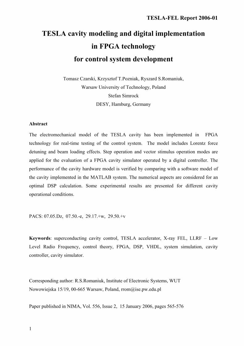
The TESLA accelerator uses nine-cell superconducting niobium resonators to accelerate
electrons and positrons. The acceleration structure is operated in a standing π-mode wave at the
frequency of 1,3 GHz. The RF oscillating field is synchronized with the motion of a particle
moving at the velocity of light across the cavity (see figure 1). The LLRF (low level radio
frequency) cavity control system for the TESLA project has been developed in order to
stabilize the accelerating fields of the resonators. The control section, powered by one klystron,
may consist of many cavities. One klystron supplies the RF power of 10 MW to the cavities
through the coupled waveguide with a circulator. The cavities are driven with pulses of 1.3 ms
in duration and the average accelerating gradients of 25 MV/m. The control feedback system
regulates the vector sum of the pulsed accelerating fields in multiple cavities. The fast
amplitude and phase control of the cavity field is accomplished by modulation of the signal
driving the klystron. The cavity RF signal is down-converted to an intermediate frequency of
250 kHz preserving the amplitude and phase information. The ADC and DAC converters link
the analog and digital parts of the system. The digital signal processing is applied for the
detection of the field vector as the complex envelope represented by real - I (in-phase) and
imaginary – Q (quadrature) components (I/Q detector). The digital controller stabilizes the
complex envelope of the cavity wave, according to the desired set point. Additionally, the
adaptive feed-forward is applied to improve the compensation of repetitive perturbations
induced by the beam loading and by the dynamic Lorentz force detuning.
TESLA-FEL Report 2006-01
3
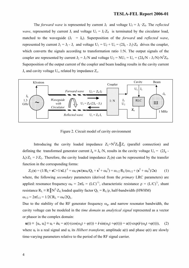
Figure 1. Cavity environment and simplified block diagram of the cavity control system
The theoretical verification of the existing superconducting cavity model [1-3] lead to
the synthesis of a digital algorithm efficiently implemented in the FPGA structure. This cavity
simulator was used for evaluation of the control algorithms and for investigation of the optimal
control method. The FPGA hardware implementation of the cavity model is intended for real
time operation.
2. The cavity model
2.1 Electrical circuit model
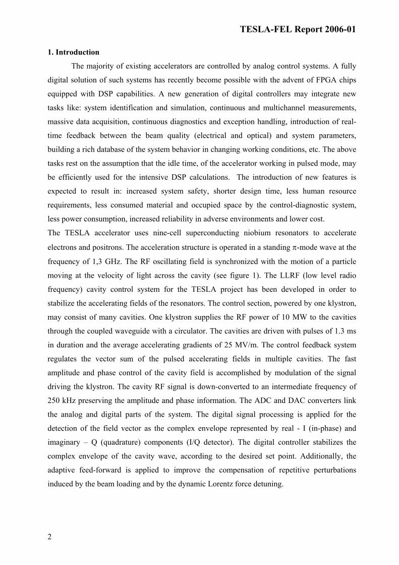
The following considerations are limited to a single cavity represented as LCR circuit
coupled to a waveguide driven by a klystron. This approach is sufficient for the purpose of
cavity control modeling [1-3]. The circuit model of the cavity environment is presented in
figure 2. The currents (J) and voltages (U) are represented in Laplace space. The klystron as a
power amplifier is modeled by the RF current generator Jk driving the waveguide via a
circulator. The waveguide, as a transmission line, is parameterized by characteristic impedance
Z0 and time delay Tw. The cavity is represented as resonant LCR circuit with impedance Zc(s) =
(1/R + sC + 1/sL)-1 coupled to the waveguide. Beam loading is modeled as a current source -Jb
supplied by the electromagnetic field of the cavity. The bunched beam current has ~2 ps pulse
duration, 1 MHz rate and an average value of 8 mA.
C O N T R O L L E R
Vector Modulator
I/Q Detector
Feed-Forward Set-point
ADC DAC
Fiel
d se
nso r
Cou
pler
Down- converter
Klystron
C A V I T Y A N A L O G S Y S T E M
Particle
TESLA-FEL Report 2006-01
4
The forward wave is represented by current Jf and voltage Uf = Jf ·Z0. The reflected
wave, represented by current Jr and voltage Ur = Jr·Z0 is terminated by the circulator load,
matched to the waveguide (Jf = Jk). Superposition of the forward and reflected wave,
represented by current J1 = Jf - Jr and voltage U1 = Uf + Ur = (2Jk - J1)·Z0 drives the coupler,
which converts the signals according to transformation ratio 1:N. The output signals of the
coupler are represented by current J2 = J1/N and voltage U2 = NU1 = Uc = (2Jk/N - J1/N)·N2Z0.
Superposition of the output current of the coupler and beam loading results in the cavity current
Jc and cavity voltage Uc, related by impedance Zc.
Figure 2. Circuit model of cavity environment
Introducing the cavity loaded impedance ZL=N2Z0Zc (parallel connection) and
defining the transformed generator current Jg ≡ Jk /N, results in the cavity voltage Uc = (2Jg -
Jb)·ZL = J·ZL. Therefore, the cavity loaded impedance ZL(s) can be represented by the transfer
function in the corresponding forms:
ZL(s) = (1/RL+ sC+1/sL)-1 = ω0·ρs/(sω0/QL + s2 + ω02) = ω1/2·RL/(ω1/2 + (s2 + ω0
2)/2s) (1)
where, the following secondary parameters (derived from the primary LRC parameters) are
applied: resonance frequency ω0 = 2πf0 = (LC)-½, characteristic resistance ρ = (L/C)½, shunt
resistance RL ≡ RN2·Z0, loaded quality factor QL = RL/ρ, half-bandwidth (HWHM)
ω1/2 = 2πf1/2 = 1/2CRL = ω0/2QL.
Due to the stability of the RF generator frequency ωg, and narrow resonator bandwidth, the
cavity voltage can be modeled in the time domain as analytical signal represented as a vector
or phasor in the complex domain:
u(t) ≡ [ur, ui] ≡ ur + iui = a(t)·(cos(ωgt + φ(t)) + i·sin(ωgt +φ(t))) = a(t)·exp(i·(ωgt +φ(t))), (2)
where ur is a real signal and ui its Hilbert transform; amplitude a(t) and phase φ(t) are slowly
time-varying parameters relative to the period of the RF signal carrier.
1.3 GHz
1 MHz
J2 U2
-Jb Jk
U1 = Z0·(2Jk - J1)
Uf = Z0·Jf
Ш
Coupler
~ 1: N
Waveguide
with Circulator
Klystron Beam
Reflected wave
Forward wave
Ur = Z0·Jr
Uc Jc
Zc
RLC
Cavity
TESLA-FEL Report 2006-01
5
The cavity current is modeled as an analytical signal j(t) = 2jg(t) - jb(t), where jb corresponds to
the ωg Fourier component of the beam loading current. The relation between the current and the
voltage is given in Laplace space:
U(s) = J(s)·ZL(s) (3)
where U(s) and J(s) = 2Jg(s) - Jb(s), are Laplace transforms of the analytical signal for the
voltage and current respectively.
The low level RF representation of the cavity signal in the time domain is the complex
envelope derived from the complex demodulation (down conversion) of the analytical signal,
which is obtained by applying the operator exp(-iωgt) for a given frequency ωg. Vice versa, the
complex modulation (up conversion) of the envelope is obtained by applying the operator
exp(iωgt) and yields the analytical signal for a given frequency ωg. The complex envelope for
the cavity current i(t) and voltage v(t) can be represented as a vector or phasor by its real I - in-
phase, and imaginary Q - quadrature components as follows (for the voltage case):
[I, Q]voltage ≡ v(t) ≡ [vr, vi] ≡ vr+ ivi ≡ u(t)·exp(-iωgt) = a(t)eiφ(t) ≡ [a(t)cosφ(t), a(t)sinφ(t)]. (4)
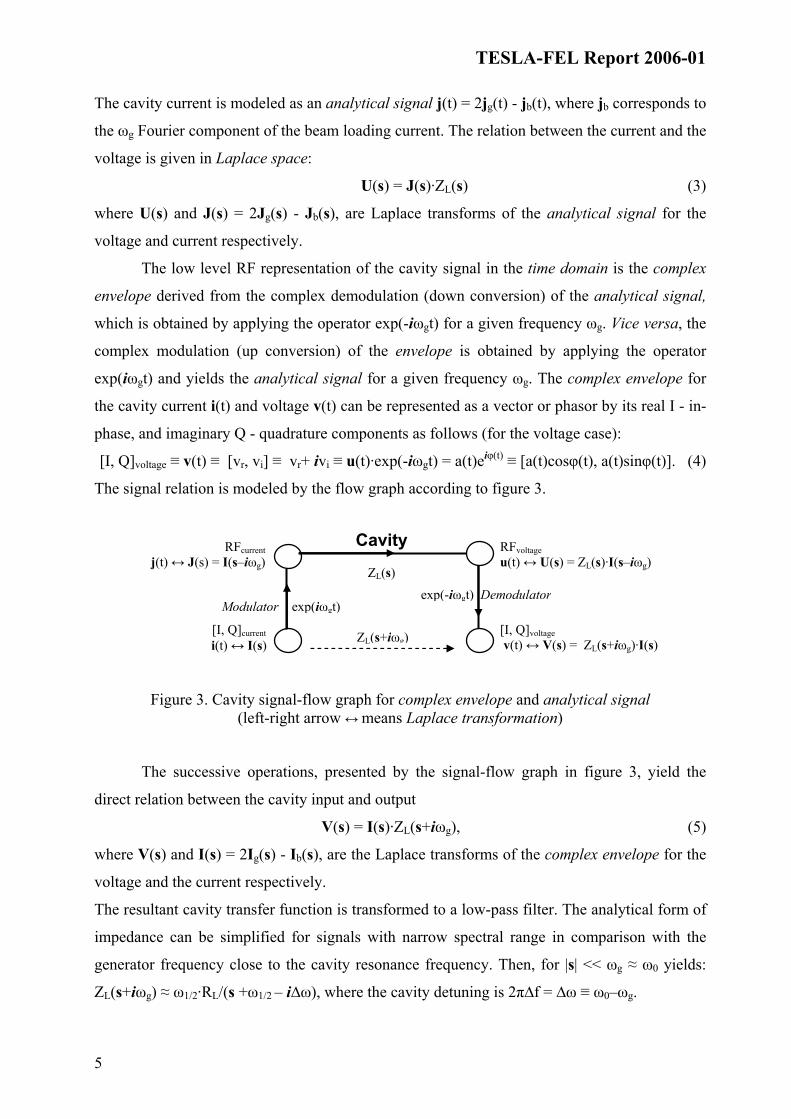
The signal relation is modeled by the flow graph according to figure 3.
Figure 3. Cavity signal-flow graph for complex envelope and analytical signal
(left-right arrow ↔ means Laplace transformation)
The successive operations, presented by the signal-flow graph in figure 3, yield the
direct relation between the cavity input and output
V(s) = I(s)·ZL(s+iωg), (5)
where V(s) and I(s) = 2Ig(s) - Ib(s), are the Laplace transforms of the complex envelope for the
voltage and the current respectively.
The resultant cavity transfer function is transformed to a low-pass filter. The analytical form of
impedance can be simplified for signals with narrow spectral range in comparison with the
generator frequency close to the cavity resonance frequency. Then, for |s| << ωg ≈ ω0 yields:
ZL(s+iωg) ≈ ω1/2·RL/(s +ω1/2 – i∆ω), where the cavity detuning is 2π∆f = ∆ω ≡ ω0–ωg.
Cavity
ZL(s)
exp(-iωgt) DemodulatorModulator exp(iωgt)
[I, Q]current i(t) ↔ I(s)
RFcurrent j(t) ↔ J(s) = I(s–iωg)
RFvoltage u(t) ↔ U(s) = ZL(s)·I(s–iωg)
[I, Q]voltage v(t) ↔ V(s) = ZL(s+iωg)·I(s) ZL(s+iωg)
TESLA-FEL Report 2006-01
6
The complex envelope relation for the cavity signals is written in Laplace space as follows:
s·V(s) = (-ω1/2 + i∆ω)·V(s) + ω1/2·RL·I(s). (6)
Moving to the time domain yields the state space equation with v(t) as a state vector of the
cavity electrical model:
dv(t)/dt = Ae·v(t) + ω1/2·RL·i(t), (7)
where v(t) and i(t) = 2ig(t) - ib(t) are the time dependent complex envelopes of the voltage and
current respectively and Ae = -ω1/2+i∆ω is the phasor.
The resultant state space equation for the complex envelope depends only on the cavity
bandwidth and detuning. This simple relationship for the cavity envelope allows for a control
system modeling within the low-level frequency range. The phasor solution of the state-space
equation for the current step input i0 is as follows
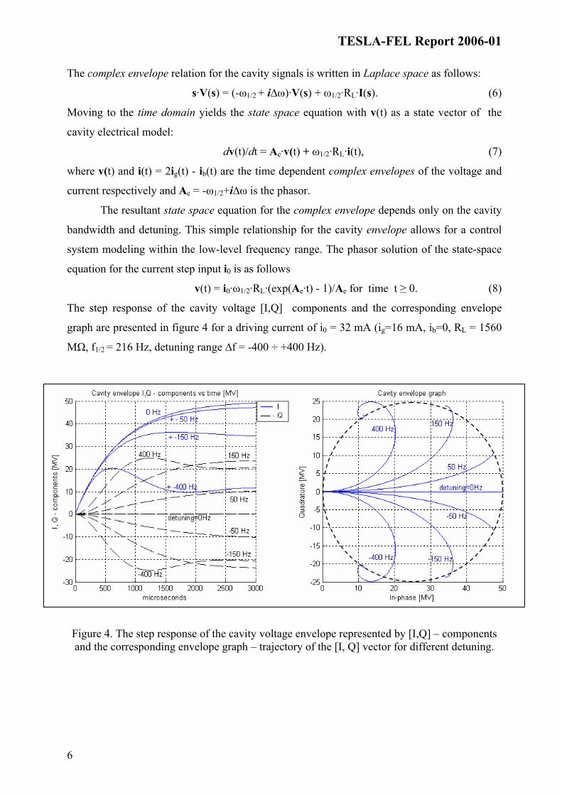
v(t) = i0·ω1/2·RL·(exp(Ae·t) - 1)/Ae for time t ≥ 0. (8)
The step response of the cavity voltage [I,Q] components and the corresponding envelope
graph are presented in figure 4 for a driving current of i0 = 32 mA (ig=16 mA, ib=0, RL = 1560
MΩ, f1/2 = 216 Hz, detuning range ∆f = -400 ÷ +400 Hz).
Figure 4. The step response of the cavity voltage envelope represented by [I,Q] – components and the corresponding envelope graph – trajectory of the [I, Q] vector for different detuning.
TESLA-FEL Report 2006-01
7
2.2. Electromechanical model
The cavity has a high loaded quality factor QL ~ 3·106 and a narrow bandwidth of
about 430 Hz (FWHM). The cavity is sensitive to mechanical distortion caused by
microphonics and Lorentz force, changing the resonator frequency. The cavity model is non-
stationary with a time varying detuning ∆ω. A value of the cavity detuning can be comparable
to the cavity bandwidth in the real operation condition. This cavity parameter has two dominant
deterministic components: the Lorentz force detuning and the initial predetuning. The
mechanically biased predetuning attempts to compensate the EM forced detuning factor, during
operation of the cavity. The mechanical model of the cavity describes the dynamic Lorentz
force detuning which depends on the time varying field gradient [2]. It is based on a linear
relationship for each of the independent mechanical modes of the cavity with resonance
frequency fm and mechanical quality factor Qm for a given mode. Each of the mechanical
equation for the m-th mode:
dwm(t)/dt = Am·wm(t) + Bm·v2(t), (9)
where wm(t) = [∆ωm(t); d[∆ωm(t)]/dt] is the state vector and consists of the time-varying
detuning ∆ωm(t) and its time derivative; Am[2x2] = [ 0,1; -(2πfm)2, -2πfm/Qm] is the system
matrix; vector Bm[2x1] = [0; - (2πfm)2·Km] is the input matrix where the parameter Km is the
Lorentz force detuning constant.
The resulting cavity detuning is ∆ω(t) = ∑∆ωm(t) + ∆ω0, where ∆ω0 is the initial predetuning.
The main parameters of the cavity electromechanical model are gathered in table 1. The
three dominating modes are considered for the mechanical model.
The pure mechanical model is weakly damped. The dominating oscillations are caused by the
mechanical modes (table 1) driven by the square of the field gradient.
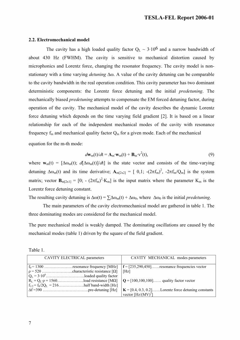
Table 1. CAVITY ELECTRICAL parameters CAVITY MECHANICAL modes parameters
f0 = 1300 …………………resonance frequency [MHz] ρ = 520 …………………..characteristic resistance [Ω] QL = 3·106………………………..loaded quality factor RL = QL·ρ = 1560………………..load resistance [MΩ] f1/2 = f0/2QL = 216……………….half band-width [Hz] ∆f =390 …………………………….pre-detuning [Hz]
f = [235,290,450]……resonance frequencies vector [Hz] Q = [100,100,100]…… quality factor vector K = [0.4, 0.3, 0.2]……Lorentz force detuning constants vector [Hz/(MV)2]
TESLA-FEL Report 2006-01
8
3. Digital processing of the cavity model
3.1 Discrete cavity model
A discrete processing of the cavity algorithm has been developed for a digital
implementation of the cavity model. The continuous model of the cavity behavior, presented in
equations (7) and (9), can be approximated by recursive calculations in a finite number of
steps. Applying the Euler approximation for time the derivative of a general variable x: dx/dt ≈
(xn+1 - xn)/T, yields for successive n-th and (n+1)-th samples, with time interval T and with
identity matrix 1, the following recursive equations, respectively:
• for the electrical model (7) in the vector representation with matrix Ae = [-ω1/2, -∆ω; ∆ω,-
ω1/2],
vn+1 = (1 + T·Ae)·vn + T·ω1/2·RL·in, where in = 2(ig)n – (ib)n, (10)
• for the mechanical m-th mode (9),
(wm)n+1 = (1 + T·Am)·(wm)n + T·Bm·(v2)n. (11)
Applying simplified notation by ignoring time indices and by introducing new symbols yields,
respectively,
• for the electrical model:
v = E*v + ig – ib, (12)
where E = [1-T·ω1/2, -T·∆ω; T·∆ω, 1-T·ω1/2] is the discrete system matrix and ig = T·ω1/2·RL·2ig
is the unified input signal for the generator and ib = T·ω1/2·RL·ib, for the beam loading,
• for the m-th mechanical mode:
wm = (1+T·Am)·wm + T·Bm·v2. (13)
Applying the common state vector w (dim = 6 x 1) and the common matrix A (dim = 6
x 6) and the common vector B (dim = 6 x 1), for the mechanical model with 3 modes, yields:
w = A*w + B*v2, (14)
where the partial vector and matrices with indices range (2m-1: 2m) for the m-th mode are
defined as: w(2m-1:2m) = wm , A(2m-1:2m, 2m-1:2m) = 12+T·Am, B(2m-1:2m) = T·Bm for m
= 1:3.
The resultant detuning of the cavity is ∆ω = ∑w(2m-1) + w0, where w0 is the initial
predetuning.
The discrete cavity algorithm, for the electrical and mechanical parallel iterative processing,
has been implemented by applying Matlab code with the sampling time T= 1µs.
TESLA-FEL Report 2006-01
9
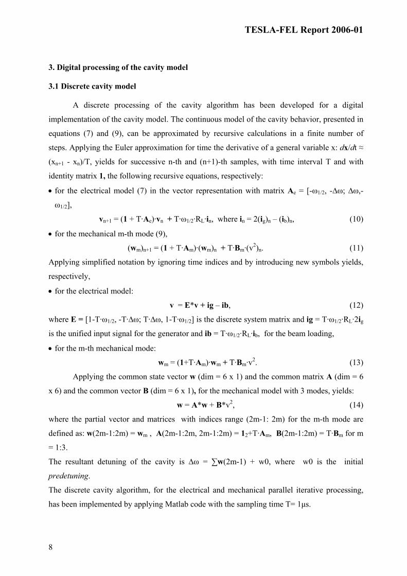
3.2 Cavity simulator algorithm
The functional diagram of the cavity digital simulator algorithm, according to the
electromechanical model, is presented in figure 5. The electrical part of the cavity simulator is
implemented in an arithmetical function block using DSP functions. The arithmetic procedure
is realized according to the state space relation with state vector v representing [I, Q]
components of the cavity output envelope. The discrete system matrix E depends on the cavity
detuning ∆ω and the cavity bandwidth ω1/2. A normalized current generator with input signal ig
and the beam ib, drives the DSP unit. The non-stationary detuning ∆ω is a parameter of the
matrix E. The input and output registers correspond to the time delay of cavity environment
(waveguide). The intermediate frequency IF modulator converts the cavity output vector to the
signal v_m of frequency 250 kHz (reciprocal operation to the I/Q detection).
Figure 5. Functional diagram of the cavity simulator algorithm
The mechanical model of the cavity is implemented in the DSP unit, according to the
state space relation, with the state vector w. The time-varying detuning and its time derivative
are two state-variables for each mechanical mode. The system matrix A and the vector B
depend on the following cavity parameters: the resonance frequency, the quality factor and the
Lorentz force-detuning constant for each mechanical mode. Each of the mechanical modes is
driven by the square of the cavity field gradient v2 generated from the electrical part of the
Input register ig
Electrical model
v = E*v + ig – ib
v_m
w
Mechanical model
w = A*w + Bv2
∆ω = w0+w(1)+w(3)+w(5)
IF modulator
v2
v
∆ω
Beam Table ib
w0
Output register
TESLA-FEL Report 2006-01
10
model. Three dominating resonance frequencies according to the table 1 are considered in the
cavity model and the superposition of all modes, together with the initial predetuning w0, yield
the resultant detuning ∆ω.
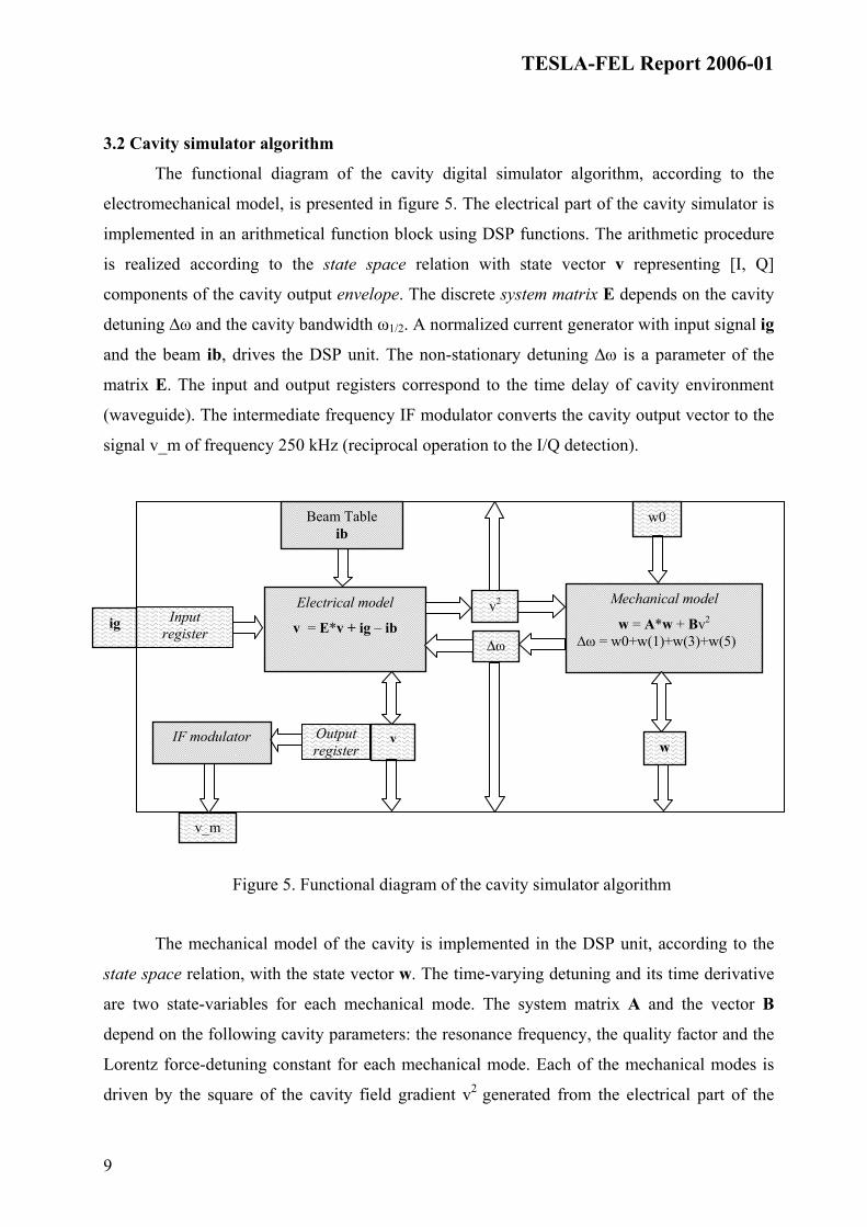
3.3 Cavity controller algorithm
A model of the control system has been developed to investigate different operational
conditions of the cavity. The functional diagram of digital controller algorithm is presented in
figure 6. The input signal v_m of intermediate frequency fi= 250 kHz from the cavity simulator
is demodulated by the I/Q detector unit. The external [I, Q] vector can be selected by the MUX
switch. The resultant cavity voltage envelope [I, Q] is calibrated, so as to compensate the
channel attenuation and phase shifting of individual cavities. The Set-Point table contains a
signal level, which is compared to the actual cavity voltage. The multiplier, working as a
proportional controller, amplifies the error signal according to the data from the GAIN table
and closes the feedback loop. The Feed-Forward table is applied and the resultant output signal
ig can drive the cavity simulator.
Figure 6. Functional diagram of the controller algorithm
3.4. DSP modeling and numerical optimization
The hardware implementation of the cavity model (discrete one) requires numerical
care due to the limited resolution of the parameters and variables of the DSP. Normalization
and scaling of the parameters and variables is an essential preparation for the DSP
implementation with fixed point arithmetic. The actual range of the involved values extends up
to seven decades (~223) for the cavity model. The best numerical accuracy for each linear
operation can be achieved by preceding scaling (multiplication by power of two) and matching
the values within the given N-bit resolution range, common for all involved quantities. The
I/Q detector
Set-Point Table
Feed-Forward Table
v_m
ig +
GAIN Table
Calibration
M
U
X I Q
+-
TESLA-FEL Report 2006-01
11
range of the scaled parameters and the maximum values of the variables has been stretched to
±2N-1 for each operation. Concluding the DSP operation, the obtained product is rescaled by bit
shifting (division by power of two) to preserve its original normalization.
The main arithmetic processing, for each actual variable xi, is a linear combination of
the corresponding variables xk with the parameter aik as follows: ∑=k
kiki xax . The equivalent
DSP operation is: ikk
kiki S/XAX ∑= , with the scaled variable Xi = si·xi with a scaling factor si,
the scaled parameter Aik = sik·aik with a scaling factor sik, the scaled variable Xk = sk·xk with
scaling factor sk, and the resultant rescaling factor Sik = sik·sk/si. The number of bits equals to
log2(Sik) for the rescaling shift and for each multiplication.
The discrete cavity model from par.3.1., was adapted for the hardware implementation.
The scaled model with integer-valued N-bit resolution was developed in the Matlab system as
the pattern for the VHDL coding for the FPGA implementation. The numerical accuracy of the
digital model was tested for different bit resolutions, and diverse scaling factors. The full bit
resolution of the MATLAB cavity model, with normalized parameters and variables, was
considered as a reference.
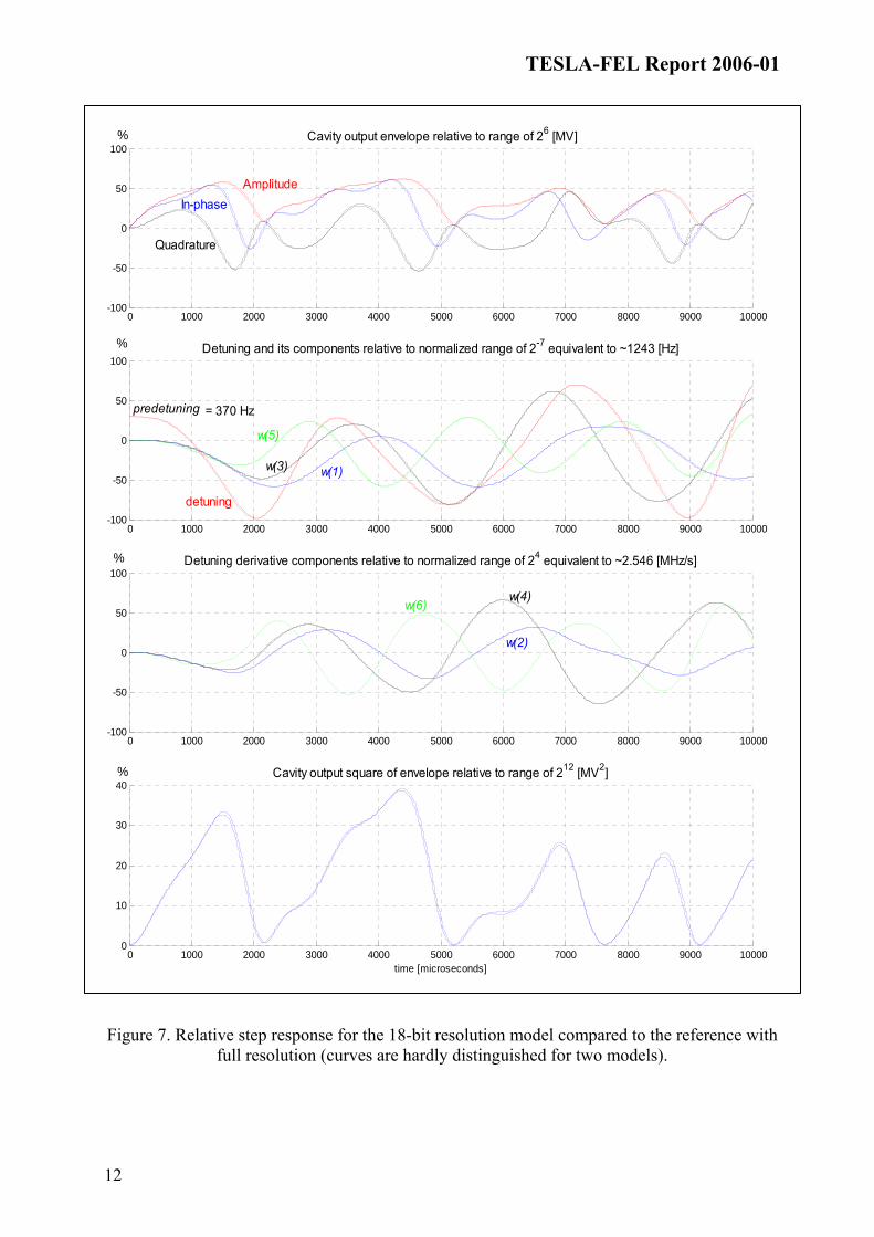
The relative step response is shown in fig.7 for all variables for the 18-bit resolution
model compared to the reference with full resolution. Two cavity models (digital 18-bit
resolution and full resolution one) were driven with the same input signal generator, equivalent
to ~14,7 mA current pulse. The total time of the simulation is 10000 µs and is long compared
to the real operating pulse of 1500 µs. Due to the good agreement the curves for two models are
hardly distinguishable.
The relative mean square error of the complex envelope Err(N) for N-bit resolution was
calculated for n steps according to the expression:
Err(N) = ∑|(VN)k - (Vref)k|2 / ∑|(Vref)k|2, for k = 1:n, (15)
where (Vref)k is the complex sample of the reference envelope for the k-th step, (VN)k is the
complex sample of the N-bit resolution envelope for the k-th step.
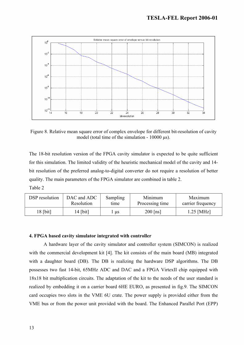
The 18-bit resolution cavity model was considered for the final hardware realization with the
relative mean square error Err(18) = 5.1e-3. The results for different bit resolutions are
presented in fig.8. However, for nonlinear systems like this they depend on the detailed
simulation conditions.
TESLA-FEL Report 2006-01
12
Figure 7. Relative step response for the 18-bit resolution model compared to the reference with full resolution (curves are hardly distinguished for two models).
0 1000 2000 3000 4000 5000 6000 7000 8000 9000 10000-100
-50
0
50
100 Cavity output envelope relative to range of 26 [MV]
AmplitudeIn-phase
Quadrature
0 1000 2000 3000 4000 5000 6000 7000 8000 9000 10000-100
-50
0
50
100Detuning and its components relative to normalized range of 2-7 equivalent to ~1243 [Hz]
detuning
w(5)
w(3) w(1)
0 1000 2000 3000 4000 5000 6000 7000 8000 9000 10000-100
-50
0
50
100Detuning derivative components relative to normalized range of 24 equivalent to ~2.546 [MHz/s]
w(6)w(4)
w(2)
0 1000 2000 3000 4000 5000 6000 7000 8000 9000 100000
10
20
30
40
time [microseconds]
Cavity output square of envelope relative to range of 212 [MV2]
predetuning = 370 Hz
%
%
%
%
TESLA-FEL Report 2006-01
13
Figure 8. Relative mean square error of complex envelope for different bit-resolution of cavity model (total time of the simulation - 10000 µs).
The 18-bit resolution version of the FPGA cavity simulator is expected to be quite sufficient
for this simulation. The limited validity of the heuristic mechanical model of the cavity and 14-
bit resolution of the preferred analog-to-digital converter do not require a resolution of better
quality. The main parameters of the FPGA simulator are combined in table 2.
Table 2
DSP resolution DAC and ADC Resolution
Sampling time
Minimum Processing time
Maximum carrier frequency
18 [bit] 14 [bit] 1 µs 200 [ns] 1.25 [MHz]
4. FPGA based cavity simulator integrated with controller
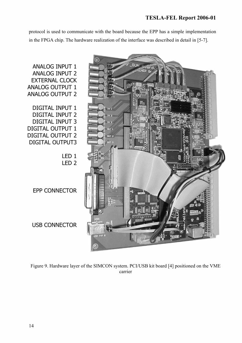
A hardware layer of the cavity simulator and controller system (SIMCON) is realized
with the commercial development kit [4]. The kit consists of the main board (MB) integrated
with a daughter board (DB). The DB is realizing the hardware DSP algorithms. The DB
possesses two fast 14-bit, 65MHz ADC and DAC and a FPGA VirtexII chip equipped with
18x18 bit multiplication circuits. The adaptation of the kit to the needs of the user standard is
realized by embedding it on a carrier board 6HE EURO, as presented in fig.9. The SIMCON
card occupies two slots in the VME 6U crate. The power supply is provided either from the
VME bus or from the power unit provided with the board. The Enhanced Parallel Port (EPP)
TESLA-FEL Report 2006-01
14
protocol is used to communicate with the board because the EPP has a simple implementation
in the FPGA chip. The hardware realization of the interface was described in detail in [5-7].
Figure 9. Hardware layer of the SIMCON system. PCI/USB kit board [4] positioned on the VME carrier
ANALOG INPUT 1 ANALOG INPUT 2 EXTERNAL CLOCK
ANALOG OUTPUT 1 ANALOG OUTPUT 2
DIGITAL INPUT 1 DIGITAL INPUT 2 DIGITAL INPUT 3
DIGITAL OUTPUT 1 DIGITAL OUTPUT 2 DIGITAL OUTPUT3
LED 1 LED 2
EPP CONNECTOR
USB CONNECTOR

TESLA-FEL Report 2006-01
15
The integrated SIMCON system is realized in form of a parameterized structure of
functional blocks in VHDL. The AD and DA converters are located on a daughter board. The
optional connection of the external control to the simulator or controller of the FEL cavity is
possible via the provided I/O ports. The digital TTL inputs, present on the VME board, were
used for synchronization with the 1MHz clock and the 10 Hz trigger. A signal of 10Hz is the
major trigger of the accelerator and 1MHz is the sampling frequency of the down-converted
signal. These signals are distributed in the existing analog generation of the whole control
system of the FEL. The functional structure of the SIMCON is presented in figure 10.
A core of the SIMCON is built of two nondependent modules: the CAVITY
SIMULTOR and the CAVITY CONTROLLER. They are programmed inside the FPGA chip
as hardware DSP algorithms. The algorithms use fast internal multiplication components. The
blocks work in parallel in real time. They are controlled by programmable parameters provided
by the PROGRAMMABLE DATA CONTROLLER block. The parameters are scalars (cavity
and controller data) and vectors (feed-forward and beam data). The set parameters stem from
the algorithms described in detail in [3].
Figure 10. Multilayer functional structure of the SIMCON
TESLA-FEL Report 2006-01
16
The block of INPUT MULTIPLEXERS allows the programmable input of the control
signals of controller and simulator blocks. Realization of the following functions is possible
through this block: internal digital feedback loops, connection of external analog signals from
AD converters, setting of test vectors initially programmed in the DAQ block (described
below). The OUTPUT SWITCH MATRIX selects different outputs to the DA converters or
data registration in DAQ block. A suitable configuration of the switch matrix gives appropriate
analog feedback between the cavity controller and simulator.
The block DATA ACQUISITION (DAQ) allows for current monitoring of the most
important signals in the system. These may be input and output signals or internal results from
the DSP processing in the algorithms of cavity simulator and controller. DAQ block is used as
programmable signal generator for the tests of the input and output signals.
The block INPUT PROCESSING provides a conversion of values between physical 14-
bit resolution of ADC converters and 18-bit resolution of internal DSP processing, the input
signal calibration including amplification and regulated shift of the constant voltage value, as
well as smoothing of the input channels (preprocessing) using a method of averaging. The
block OUTPUT PROCESSING provides conversion between physical 18-bit resolution of the
internal DSP processing and 14-bit resolution of DAC.
The block TIMING & STATUS CONTROLLER provides internal synchronization of
all processes of the SIMCON system. It selects between the external clock signals provided by
the accelerator control system or clocks from external generators. The latter case enables
autonomous work of the system. Switching of the operation modes of the system is possible,
i.e. performing simulation in real time or in the step simulation regime with reference vectors.
The programming layer of all blocks of SIMCON system is realized by the control
computer system with the aid of the COMMUNICATION CONTROLLER block. The EPP
hardware transmission protocol was used for this purpose. The signal distribution bases on the
Internal Interface standard, described in detail in [7].
The step operation and vector stimulus mode is applied for testing the FPGA device
coupled to the MatLab system via the COMMUNICATION CONTROLLER. The FPGA
signal processing was verified according to the desired algorithm. To realize online processing,
a synchronous 40MHz pipeline bus is used. The system flexibility, obtained in this way, gives
the possibility to choose arbitrarily the number of clock periods necessary to do the successive,
partial calculations by the DSP blocks.
TESLA-FEL Report 2006-01
17
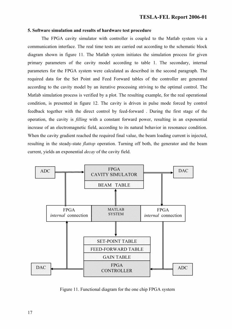
5. Software simulation and results of hardware test procedure
The FPGA cavity simulator with controller is coupled to the Matlab system via a
communication interface. The real time tests are carried out according to the schematic block
diagram shown in figure 11. The Matlab system initiates the simulation process for given
primary parameters of the cavity model according to table 1. The secondary, internal
parameters for the FPGA system were calculated as described in the second paragraph. The
required data for the Set Point and Feed Forward tables of the controller are generated
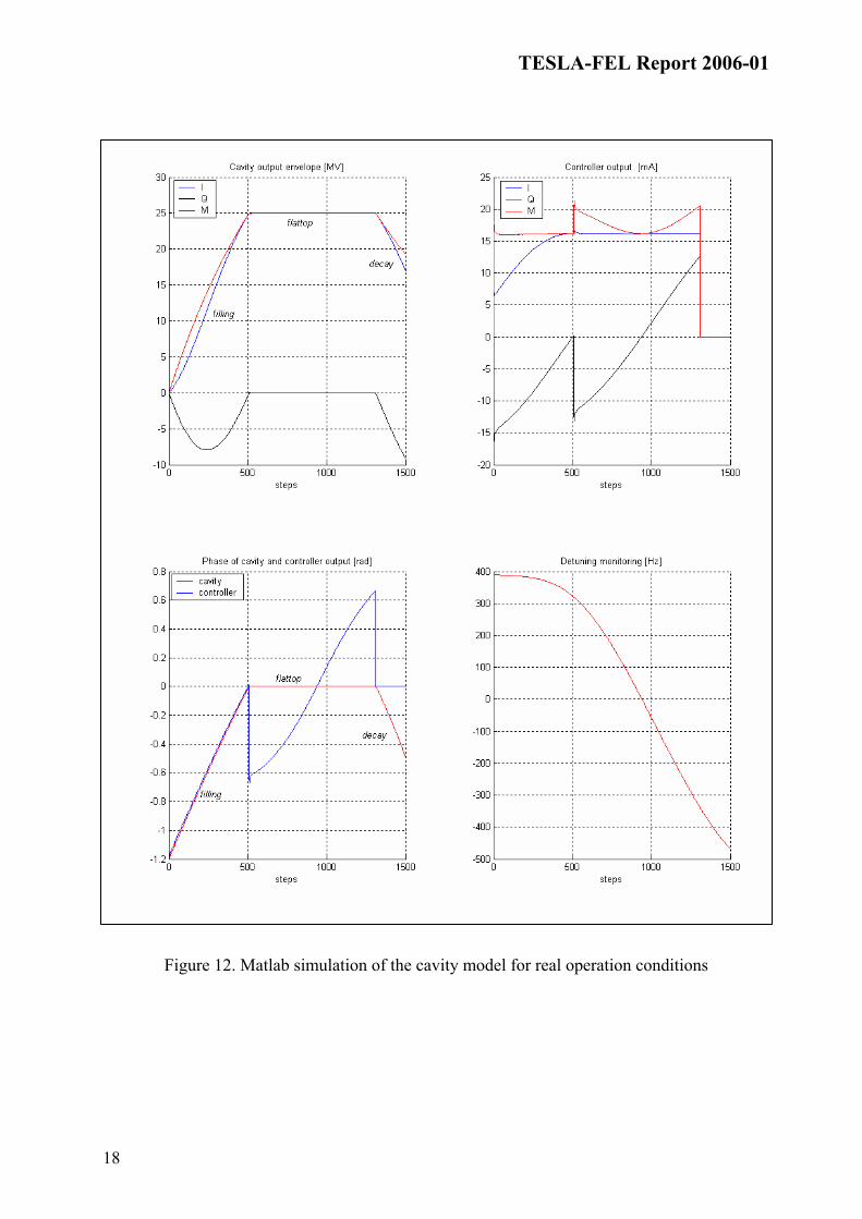
according to the cavity model by an iterative processing striving to the optimal control. The
Matlab simulation process is verified by a plot. The resulting example, for the real operational
condition, is presented in figure 12. The cavity is driven in pulse mode forced by control
feedback together with the direct control by feed-forward . During the first stage of the
operation, the cavity is filling with a constant forward power, resulting in an exponential
increase of an electromagnetic field, according to its natural behavior in resonance condition.
When the cavity gradient reached the required final value, the beam loading current is injected,
resulting in the steady-state flattop operation. Turning off both, the generator and the beam
current, yields an exponential decay of the cavity field.
Figure 11. Functional diagram for the one chip FPGA system
FPGA internal connection
FPGA CAVITY SIMULATOR
FPGA CONTROLLER
MATLAB SYSTEM
BEAM TABLE
FEED-FORWARD TABLE
SET-POINT TABLE
FPGA internal connection
DAC
DAC
ADC
ADC
GAIN TABLE
TESLA-FEL Report 2006-01
18
Figure 12. Matlab simulation of the cavity model for real operation conditions
TESLA-FEL Report 2006-01
19
The resulting parameters and data are loaded to the FPGA internal memory. The
controller can drive the cavity simulator via the internal digital connection (18-bit data
resolution). The FPGA system can run itself cyclically according to the given data tables. The
cavity simulator and controller can be also driven independently via the external connection
applying 14-bit ADC. The 14-bit DACs convey data from the cavity simulator or from
controller outside FPGA system.
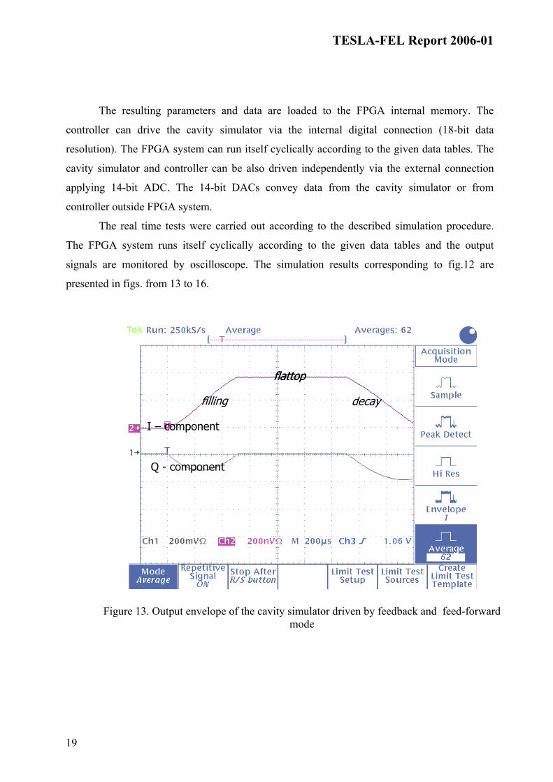
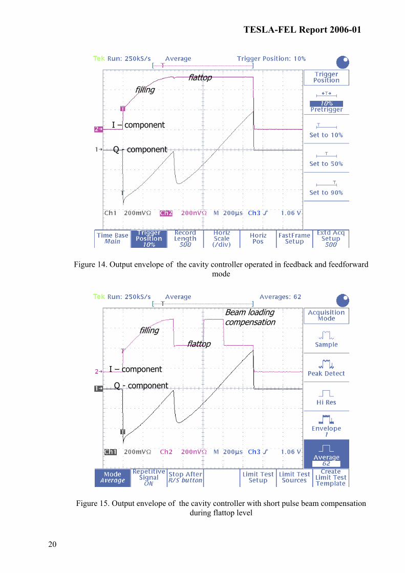
The real time tests were carried out according to the described simulation procedure.
The FPGA system runs itself cyclically according to the given data tables and the output
signals are monitored by oscilloscope. The simulation results corresponding to fig.12 are
presented in figs. from 13 to 16.
Figure 13. Output envelope of the cavity simulator driven by feedback and feed-forward mode
I – component
flattop
filling decay
flattop
Q - component
TESLA-FEL Report 2006-01
20
Figure 14. Output envelope of the cavity controller operated in feedback and feedforward mode
Figure 15. Output envelope of the cavity controller with short pulse beam compensation during flattop level
Q - component
filling flattop
Beam loading compensation
I – component
I – component
Q - component
filling
flattop
TESLA-FEL Report 2006-01
21
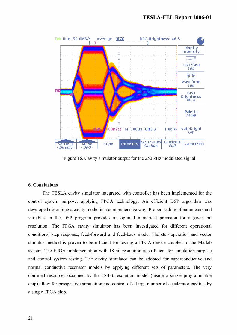
Figure 16. Cavity simulator output for the 250 kHz modulated signal
6. Conclusions
The TESLA cavity simulator integrated with controller has been implemented for the
control system purpose, applying FPGA technology. An efficient DSP algorithm was
developed describing a cavity model in a comprehensive way. Proper scaling of parameters and
variables in the DSP program provides an optimal numerical precision for a given bit
resolution. The FPGA cavity simulator has been investigated for different operational
conditions: step response, feed-forward and feed-back mode. The step operation and vector
stimulus method is proven to be efficient for testing a FPGA device coupled to the Matlab
system. The FPGA implementation with 18-bit resolution is sufficient for simulation purpose
and control system testing. The cavity simulator can be adopted for superconductive and
normal conductive resonator models by applying different sets of parameters. The very
confined resources occupied by the 18-bit resolution model (inside a single programmable
chip) allow for prospective simulation and control of a large number of accelerator cavities by
a single FPGA chip.
TESLA-FEL Report 2006-01
22
Acknowledgments
We acknowledge the support of the European Community Research Infrastructure Activity under the FP6 "Structuring the European Research Area" program (CARE, contract number RII3-CT-2003-506395). The authors would like to thank DESY Directorate for providing excellent conditions to perform the work described in this paper.
References
1. T. Schilcher, “Vector Sum Control of Pulsed Accelerating Fields in Lorentz Force Detuned
Superconducting Cavities”, Ph. D. thesis, Hamburg, 1998
2. M. Liepe, W.D.-Moeller, S.N. Simrock, “Dynamic Lorentz Force Compensation with a
Fast Piezoelectric Tuner” in Proc. of the 2001 Particle Accelerator Conference, Chicago
3. T. Czarski, R.S. Romaniuk, K.T. Pozniak, S. Simrock, “Cavity Control System, Advanced
Modeling and Simulation for TESLA Linear Accelerator”, TESLA Technical Note, 2003-
06, DESY
4. http://www.nallatech.com/ [Nallatech Homepage]
5. K.T. Pozniak, T. Czarski, R. S.Romaniuk, “Functional Analysis of DSP Blocks in FPGA
Chips for Application in TESLA LLRF System”, TESLA Technical Note, 2003-29, DESY
6. K.T. Pozniak, R.S. Romaniuk, K. Kierzkowski, “Parameterized Control Layer of FPGA
Based Cavity Controller and Simulator for TESLA Test Facility”, TESLA Technical Note,
2003-30, DESY
7. K.T. Pozniak, M. Bartoszek M. Pietrusinski, “Internal Interface for RPC Muon Trigger
electronics at CMS experiment”, Proceedings of SPIE, Photonics Applications II In
Astronomy, Communications, Industry and High Energy Physics Experiments, Vol. 5484,
2004


![[Tesla Nickola] the Strange Life of Nikola Tesla(BookFi.org)](https://img.pdfslide.us/doc/110x75/55cf9cb0550346d033aab3ce/tesla-nickola-the-strange-life-of-nikola-teslabookfiorg.jpg)