Embed Size (px)
Citation preview

Fast Assembly of Gold Nanoparticles in Large-Area
2-D Nanogrids Using a One-Step, Near-Infrared
Radiation-Assisted Evaporation Process
André Utgenannt,a Ross Maspero,a,b Andrea Fortini,a Rebecca Turner,a Marian Florescu,a,b
Christopher Jeynes,c Antonios G. Kanaras,d Otto L. Muskens,d Richard P. Sear,a
and Joseph L. Keddiea*
a. Department of Physics, University of Surrey, Guildford, Surrey GU2 7XH, UK
b. Advanced Technology Institute, University of Surrey, Guildford, Surrey GU2 7XH, UK
c. Ion Beam Centre, University of Surrey, Guildford, Surrey GU2 7XH, UK
d. Physics and Astronomy, Faculty of Physical Sciences and Engineering, University of
Southampton, Highfield, Southampton, SO17 1BJ, UK
1
ABSTRACT
When fabricating photonic crystals from suspensions in volatile liquids using the horizontal
deposition method, the conventional approach is to evaporate slowly to increase the time for
particles to settle in an ordered, periodic close-packed structure. Here, we show that the greatest
ordering of 10 nm aqueous gold nanoparticles (AuNPs) in a template of larger spherical polymer
particles (mean diameter of 338 nm) is achieved with very fast water evaporation rates obtained
with near-infrared radiative heating. Fabrication of arrays over areas of a few cm2 takes only
seven minutes. The assembly process requires that the evaporation rate is fast relative to the
particles’ Brownian diffusion. Then a two-dimensional colloidal crystal forms at the falling
surface, which acts as a sieve through which the AuNPs pass, according to our Langevin
dynamics computer simulations. With sufficiently fast evaporation rates, we create a hybrid
structure consisting of a two-dimensional AuNP nanoarray (or “nanogrid”) on top of a three-
dimensional polymer opal. The process is simple, fast and one-step. The interplay between the
optical response of the plasmonic Au nanoarray and the microstructuring of the photonic opal
results in unusual optical spectra with two extinction peaks, which are analyzed via finite-
difference time-domain method simulations. Comparison between experimental and modelling
results reveals a strong interplay of plasmonic modes and collective photonic effects, including
the formation of a high-order stop band and slow-light enhanced plasmonic absorption. The
structures, and hence their optical signatures, are tuned by adjusting the evaporation rate via the
infrared power density.
KEYWORDS
2

Self-assembly, plasmonics, photonics, coupling, gold nanoparticles, inverse opal, evaporation, IR
heating
Periodic nanostructures have a wide range of applications including antireflection coatings,1
self-cleaning films,2 sensors,3,4 meta-materials,5 and devices for energy-harvesting.6 Among the
methods for the fabrication of periodic nanostructures, self-assembly methods are particularly
attractive because of their numerous benefits, including low costs and simple processing steps.7
Vertical8 and horizontal9 deposition of nanoparticles from a carrier solvent are established
methods for the fabrication of periodic nanostructures.
For both types of deposition method, several groups have investigated how the quality of an
ordered nanoparticle assembly is affected by various parameters, e.g. the evaporation
rate (controlled via humidity,10 air pressure,11 solvent volatility,12 etc.), the withdrawal speed of
the plate in confined geometries,13 the particle concentration, and the particle size ratio in
bimodal blends.14 Horizontal deposition is considered to be a low-cost and fast method with the
ability to be employed in the large-scale fabrication of colloidal crystals.15 Its main advantage
lies in its ease of use and relatively low technical difficulty compared to vertical deposition
methods. The environmental conditions (for example, the temperature, pressure and humidity)
during the drying process have a pronounced influence on the structure obtained via the
horizontal deposition method. However, according to previous reports, the method typically
suffers from long drying times, which are conventionally used in colloidal crystallization from
liquids to obtain a high degree of periodicity and order.16 This time inefficiency presents a major
obstacle to the widespread adoption of the horizontal deposition method.
The aim of most published work on particle assembly is to create either 2D structures
(colloidal monolayers, nanomeshes,17,18 ring structures,4 and arrays of nanocavities19) or 3D
3

structures (opals and inverse opals). In recent years, hybrid colloidal crystals, which consist of
2D plasmonic arrays on photonic crystals,20 are of growing interest. Hybrid structures combine
aspects of plasmonics and photonics.21 The strong synergetic effect of plasmon excitation and the
photonic band gap results in materials with advanced optical functionalities that enable the
control of the propagation, emission and extinction of light on the nanoscale. These materials
represent a promising platform for novel light sources and sensors.20 The broad variety of designs
for 2D nanoarrays and 3D structures results in a vast number of possible hybrid architectures.
Hence, a rapid fabrication method will be highly beneficial to progress in this field.
Here, we introduce a fast, efficient and low-cost fabrication method to achieve the colloidal
self-assembly of a hybrid structure consisting of a (quasi) two-dimensional (2D) gold
nanoparticle network (which we call a “nanogrid”) and a three-dimensional binary colloidal
crystal (3D bCC). Surprisingly, a highly-ordered periodic nanostructure is only obtained with a
high evaporation rate induced with infrared radiative heating. In our previous work, we spatially
modulated the infrared power density across the surface a wet colloidal film.22 We showed that
nanoparticles could be transported laterally in the plane of the film to create dome-like surfaces
in a periodic array. In the present work, we have discovered that the fast evaporation rates
obtained with infrared heating drives assembly of nanoparticles at the descending film surface.
We show how the ordering of the nanostructure benefits from shorter fabrication times, which
contradicts the commonly-held belief that slow drying with long assembly times is needed to
obtain structures with a high degree of periodicity. Additionally, we show that the surface
morphology of the hybrid structures obtained can be adjusted simply by changes in the
evaporation rate without the need for a sophisticated experimental set-up or additional processing
steps.
4

The combination of the controlled materials fabrication with advanced structural
characterization and optical experiments allows us to relate the specific structure of these new
hybrid plasmonic-photonic crystals with their optical properties. An intricate interplay between
plasmonic resonances and photonic band structure effects is found which shows the promise of
fast evaporative techniques in achieving new types of hybrid optical materials.
Results and Discussion
Fabrication, optical properties and structure of colloidal nanogrids
Stabilized gold nanoparticles (AuNPs), approximately 10 nm diameter, in water were blended
with spherical acrylic copolymer particles (338 nm) in water.22 The dispersions were cast as films
and dried over a range of evaporation rates, which are expressed as the velocity at which the
water surface falls downward during drying, and which were determined experimentally.
Figure 1a shows UV-Vis-NIR spectra from a series of dried thick films of AuNP/polymer
particle blends fabricated using different evaporation rates, E, in descending order between 2.08
× 10–6 m s–1 and 0.36 × 10⁻⁶ m s–1. This range of Ewas achieved by using near infrared (NIR)
radiative heating with a corresponding range of power densities. The spectra obtained from films
dried normally under ambient conditions (E = 1.1 × 10⁻⁷ ms-1) and slowly-dried under high
humidity (E = 3.2 × 10⁻⁹ ms-1) are included for comparison. The spectrum of the fastest dried
film shows two pronounced peaks with maxima at λmax,I = 574 nm and λmax,II = 716 nm. The
intensities of the peaks weaken when the evaporation rate is slowed, even though the gold
concentration in all films is identical. Moreover, the assembly time increases from only seven
min. for the fastest evaporation rate to more than two hr. under ambient conditions.
5

Notably, the spectra for the normally and slowly dried films show only a broad extinction
across the whole range of measured wavelengths without any specific spectral features as a
signature of a periodic structure. Periodically-structured materials show a specific optical
response, for example, through extinction over a certain wavelength range. Variations in the
structure cause changes in the spectrum, which are visible through shifts of peaks and an increase
or decrease in the signal intensity.23,24 The development of the spectra in Figure 1a strongly
indicates that a highly periodic structure can be fabricated on a short time scale through rapid
drying in a horizontal deposition process.
The SEM images in Figures 1b-d show the surface structure that was fabricated using the
fastest evaporation rate (E = 2.08 × 10⁻⁶ m s–1). In these images, the polymer particles appear
dark, and the AuNPs appear white. The polymer particles are arranged in ordered hexagonal
arrays at the surface, and the AuNPs are arranged in connected rings around the larger particles.
A fast Fourier transform of Figure 1c, shown inset in 1d, confirms the nearly perfect hexagonal
symmetry of the polymer particle array. The mean center-to-center distance of the polymer
particles is 351 ± 2 nm, which is only slightly greater than the distance found in the absence of
the AuNPs (see Table S1 and Figure S1 in Supporting Information). Hence, we conclude that the
polymer particles are in close contact, and the AuNPs are resting in the valley space between
particles, with no more than a single AuNP layer separating the larger polymer particles. In the
following discussion, we describe the AuNP arrangement as a nanogrid.
Rutherford backscattering (RBS) analysis was conducted to determine the vertical distribution
of the AuNPs within the films (normal to the substrate). Figure 1e shows that there is a high
concentration of Au, cAu, at the top surface in the nanogrid, above a depleted layer, which is
attributed to the first layer of polymer particles. The 10 nm AuNPs are small enough to occupy
6

the voids between the close-packed polymer particles in the underlying layers. The first three
layers of polymer particles can be identified through the oscillation in cAu (labelled as A-C in
Figure 1e). The spacing between the marked peaks is on the same order of magnitude as the
polymer particle diameter. Deeper layers cannot be identified because of energy straggling
effects of the ions. The labels (i-iv) mark the positions of AuNP enrichment, which are presumed
to correspond to the 2D nanogrid layer at the top and the planes of AuNPs filling the interparticle
space between the hexagonally-packed layers, as is schematically illustrated in the inset diagram.
The wavelength of the oscillations in the Au concentration closely matches the spacing of the
hexagonally-packed layers in a colloidal crystal of 338 nm particles. We found that if the
structure was heated at 340 °C in a convection oven for 7 min. to sinter the AuNPs, the polymer
phase could thereafter be dissolved in toluene to leave a free-standing nanogrid sheet, as is
shown in Figure 1f.
7

Figure 1. a) UV-Vis-NIR spectra of Au/polymer hybrid films fabricated with decreasing E: i)
2.08; ii) 1.81; iii) 0.93; iv) 0.67; and v) 0.36 (all × 10–6 m s–1). The spectra for films normally
dried in the ambient atmosphere (---, E = 1.1 × 10⁻⁷ ms-1) and slowly dried under high humidity
(∙∙∙,E = 3.2 × 10⁻⁹ ms-1) films are shown for comparison. b) SEM image of a rapidly dried film (E
= 2.08 ∙ 10–6 m s–1) at the highest magnification where individual AuNPs are visible. The AuNPs
crystallize into truncated triangular-like shapes (outlined with a dashed line) and connected by
bridges (indicated by the arrow). Scale bar is 100 nm. c) At lower magnifications, it is apparent
that the larger polymer particles are in an ordered hexagonal array and the AuNPs create a grid-
like structure. Scale bar is 200 nm. d) At the lowest magnification, the formation of grain
boundaries between the 2D crystals is visible. Scale bar is 20 m. Inset: The fast Fourier
transformation (FFT) of the nanogrid structure in Figure 1c shows clearly that a hexagonal
symmetry is well established. e) Au concentration depth profile obtained from RBS analysis of a
rapidly-dried structure (E = 2.08 × 10⁻⁶ m s–1). The high Au concentration at the surface (> 8 at.
%) represents the nanogrid layer (labelled as i on the profile and on the inset diagram). The
labels on the concentration profile mark the first three layers of polymer particles (A-C) in a
closed-packed FCC crystal and the AuNP enriched voids (ii-iv) as schematically illustrated in the
inset diagram. The dashed line represents the concentration corresponding to a hypothetical
homogenous distribution of the AuNPs. Note: The inset diagram is not drawn to scale. f)
Examples of free-standing grid structures obtained from sintered AuNPs after dissolving the
polymer phase. Scale bar is 200 nm.
In summary, the results of the RBS analysis in combination with SEM indicate a hybrid
structure, which consists of a 3D binary colloidal crystal (close-packed polymer particles in
8

which the interstitial space contains AuNPs) with a 2D nanogrid structure at the surface. The
mechanism of the structure formation is considered next.
Influence of Evaporation Rate on Particle Ordering and Structuring
The vertical distribution of colloidal particles in a drying layer is determined by a competition
between evaporation, which sweeps up particles at the top surface, and diffusion, which
redistributes the particles evenly. For a film with an initial thickness of H, the rates of the two
processes are compared via a Péclet number, given as Pe = HE/DS, where DS is the Stokes-
Einstein diffusion coefficient of the particles.25 Only when Pe > 1, and evaporation is fast relative
to diffusion, will particles accumulate near the top of the drying film surface. When Pe < 1,
diffusion is fast relative to evaporation, and hence the particles will be distributed uniformly in
the direction normal to the substrate during the drying process. D is inversely related to particle
size through the Stokes-Einstein equation, which means that slower-diffusing large particles are
more prone to be found at the surface of a drying film compared to small particles.
In blends of large and small particles, each population of particles has a Péclet number,
represented as PeL and PeS, respectively. In the regime where PeS < 1 < PeL, a diffusive model26
predicts that stratification of particles by size will occur, with a greater concentration of large,
slow-diffusing particles developing at the top surface. However, our experiments using NIR-
assisted heating, in which Eis fast, are in the regime where PeL and PeS both have values well
above 1. Values of Pe range from 3.4 to 17.7 (using the hydrodynamic radius and the relevant
drying temperatures), and PeL/PeS = RL/RS. Consequently, the polymer particles and AuNPs are
both predicted to accumulate at the top surface during drying. Furthermore, according to the
model developed by Cardinal et al.,27 the sedimentation of particles on the time-scale of drying is
not significant in the experiments reported here.
9

SEM analysis of the surfaces of the films shows that periodic grid-like structures are formed
over a range of evaporation rates obtained under NIR radiation for three sizes of polymer
particles (mean diameters of 147, 261 and 338 nm). (See Figure S2 in Supporting Information).
As Eis increased, the quality of the periodic ordering, determined from quantitative image
analysis, likewise increases. (See Figure S3 in Supporting Information.) The same positive
correlation between the structure ordering and the evaporation rate was obtained for all three
particle size ratios (32.5:1, 25.1:1, and 14.1:1). A simple geometric argument shows that small
particles can pass through the holes in a plane of a close-packed array of larger particles, 26
provided that the latter are larger by a factor of ( 2√3
−1)−1
≈ 6.5. However, for particle blends
with a size ratio of 14.1:1, the ring-like structures of the nanogrid are found only with
evaporation rates above ca. 110-6 m s-1 (Figure S2). At lower rates, the AuNPs appear only in
sub-surface interparticle spaces. For this blend, in which there is a greater geometric restriction, a
faster evaporation rate is required for the AuNPs to be forced to the surface.
The surface structures of normally-dried films, which lacked any strong optical extinction,
were also examined. In this experiment, PeS is ca. 1, which is the tipping point below which the
AuNPs will not accumulate at the top of the drying film. To achieve the lower evaporation rate,
the dispersion was dried at room temperature, which is below the glass transition temperature, Tg,
of the polymer. Hence, the polymer particles are not deformed from their spherical shape, and
they do not coalesce. A representative SEM image (Figure S4a, Supporting Information) shows
that only a small number of AuNPs are seen on the film surface, appearing in the images as small
bright spots. With slow drying, achieved under high humidity, Pes takes a low value of 0.03. In
this regime, AuNPs appear only in a few isolated domains and in chains along colloidal crystal
boundaries (Figure S4b). Nanogrid structures do not develop. The Au concentration profile with
10

a normal evaporation rate shows AuNP depletion in the first µm beneath the surface and then
approaches the expected bulk concentration. (See the RBS analysis in Figure S4c of the
Supporting Information.) With slow drying, there is a very low concentration of Au at the
surface, and it gradually increases in concentration over a depth of 4 m into the surface. Only in
the high-Pe regime obtained with NIR heating are the AuNPs found to accumulate in a nanogrid
array at the top surface.
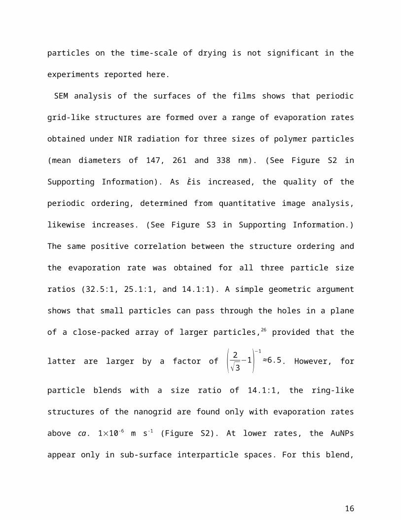
Simulations of the Structure Formation during Drying
We use Langevin dynamics simulations for particles in a solvent to explain the formation of
the nanogrid of AuNPs. The Supporting Information provides details of the simulations. We
model evaporation by a moving wall that pushes the particles toward the underlying substrate.
Figures 2a-e illustrate the evolution of the system for a blend of large and small particles with a
size ratio RS:RL = 32:1 (similar to our experiments). Both species accumulate at the air/water
interface, but the large particles form crystalline layers, while the small particles fill the
interstitial spaces. The crystal of large particles grows downward from the surface, while the
thickness of the layer of small particles also increases with time (see Figure S5 in Supporting
Information). The small particles move readily through the voids between the large particles to
reach the top surface. This is clear in Movie 1 in the Supporting Information. One can think that
the downward moving crystal acts as a “sieve” for the small particles, which move up through
the holes in the sieve, to create the periodic nanogrid array shown in Fig. 2f, which appears very
similar to the experimental structure in Figure 1c.
Our simulations neglect the forces due to the hydrodynamic flow of the evaporating water, but
we obtain very similar nanostructures in experiment and simulation. The nanogrid appears to be
11

a robust result, which is insensitive to flow forces. Our mechanism simply relies on particles of
both sizes being pushed towards the surface. The downward movement of the air/water interface
and the flow forces both push the particles in the same way.
Figure 2. Simulation snapshots showing the particles accumulating at the model air-water
interface with an evaporation rate E=12 R s /τB .Here, τ B=4 R s2/ DSis the simulation time unit; it
takes of order one unit of time for a small particle to diffuse a distance equal to its own radius.
The radius of the large (blue) particles is 32 times greater than the small (yellow) particles. We
calculate DS for the AuNPs in our experiments to be 1.1 × 10⁻¹² m2s-1 such that B 420 s. a) At
time t =0, the system is at equilibrium and evaporation is started. b) At time t = 50 τB, both
species are accumulating at the interface. c) At time t = 130 τB, the large particles start to form
ordered layers at the interface. d) At time t = 210 τB, the large particles have formed crystalline
layers at the interface, with small particles filling the interstitial spaces. e) At time t = 410 τB, the
structure formed by the large particles has not changed, but the layer of small particles has
increased its thickness. f) Top view of the nanogrid of small particles at t=410 τB.
Control of Surface Topography via the Evaporation Rate
12

With the aim of explaining the difference in the optical properties when the evaporation rates
are changed, the surface structures were examined quantitatively by atomic force microscopy
(AFM). In the AFM images presented in Figures 3a – c, the surface morphology of the films is
seen to change from a convex to a concave structure as the evaporation rate is increased. The
transition in the surface morphology is attributed to the increasing velocity of the downward
moving sieve, consisting of the close-packed polymer particles. The evaporation rates set the
velocity at which the sieve drops downwards. At a low velocity of the sieve, the AuNPs are
pushed through the holes in the sieve and start to fill the interparticle spaces between the dome-
like polymer particles (Figure 3a). When the velocity of the downward moving sieve is
increased, the AuNPs start to pile up on the film surface and exceed the level of the domes of the
polymer particles (Figure 3b). Finally, at the highest velocity, the AuNPs crystallize into the
truncated triangular-like shapes which are connected by bridges (Figure 3c), as were already
shown in Figure 1b, resulting in a protruding grid nanostructure.
13

Figure 3. AFM topographic images to show the surface morphology as a function of the
evaporation rate: a) 3.5 10-7 m s-1; b) 9.3 10-7 m s-1; and c) 20.8 10-7 m s-1. The scan size is
1.5 µm 1.5 µm for all three images. When Pes is increased from 3.4 to 17.7 (through an
increase in E), the 10 nm AuNPs pile up and build a protruding nanogrid structure. d) Line
traces of the surface topography for the three structures shown in a – c. e) A plot of the peak-to-
valley height of the film surface as a function of the evaporation rate.
The corresponding 2D line traces are shown in Figure 3d. Here, the peak-to-valley height, PV,
is defined as the difference in the height at the polymer particle center and at the polymer particle
boundary. A positive PV is obtained for the convex structure formed by the domes of the
polymer particles, and a negative PV arises from the concave honeycomb structure with the
AuNPs protruding from the surface. As a means to quantify the changes in the surface
14

morphology, PV is plotted as a function of evaporation rate (see Figure 3e). As can be seen in
this figure, PV decreases continuously with increasingE. Faster evaporation rates lead to the
AuNPs being pushed higher above the polymer particle surface. At slower evaporation rates, the
sieve effect is weaker, and perhaps there is less upward flow. Hence, AuNPs are not pushed
through the interstices of the larger polymer particles. These observations of the changing
surface morphology present interesting routes to tailor the surface properties of a highly-ordered
nanostructure simply by changes in the evaporation rate, and without the need for any
sophisticated equipment or multiple processing steps.
An important finding is that with the fastest evaporation rates achieved with NIR heating, the
arrays of AuNPs protrude upward from surface. In turn, the protruding nanogrid structure is a
requirement for the observed optical signatures, which are described in detail next.
Optical Response of Nanogrids
The optical properties of the optimized nanogrid structures were investigated using broadband
angle-dependent spectroscopy and optical microscopy. The optimized samples correspond to the
structures that were dried rapidly, with the highest evaporation rate of E = 2.08 × 10⁻⁶ m s–1.
A microscope spectrometer setup was used to map the reflection across an area of 20 µm × 20
µm. In these scans, an area including both the nanogrid structure and grain boundaries was
selected when viewing with a CCD camera. The dark-field image, obtained with this camera, is
presented in Figure 4a. The grain boundaries can be easily identified through the strong
reflection of the incident white light; the scanned area is indicated by the red box. The scans
15
were performed at three fixed wavelengths of 570 nm, 750 nm, and 890 nm. These wavelengths
of interest were selected because they are close to the maximum peak positions in the extinction
and reflection spectra in Figure 1a. The reflection map for λ = 570 nm shows generally a weak
reflection except for some regions in the grain boundaries (Figure 4b). At λ = 750 nm the overall
reflection starts to increase, as can be seen in Figure 4c. At λ = 890 nm, only the hybrid structure
shows a strong reflection (Figure 4d).
Spectroscopic information was collected at two spots in the 2D image corresponding to the
center of the hybrid colloidal crystal/nanogrid domain and the grain boundary. Good agreement
is obtained between the microscopic spectra of the hybrid and the macroscopic UV-Vis spectra
(Fig. 1a) in the positions of the peaks. Differences are visible in the values for extinction
intensities. These differences can have their origin in the difference in collection angles for the
UV-Vis and the microscopy setup, the latter collecting a larger fraction of near-forward scattered
light. Figures 4e and f show that the extinction spectrum with the two peaks is characteristic for
the hybrid crystal structure. Also the reflection spectrum shows a sharp peak (with a center
wavelength of λmax = 890 nm) only for the hybrid structure.
The position of the first-order stopband for the opal photonic crystal is given by the condition
a/ 0.6, where a=√2d the lattice period, with d = 2RL, the colloidal polymer particle diameter.
With d = 338 nm, the stopband is expected at 797 nm. The position for the photonic reflection
from the hybrid structure is red-shifted (by ca. 100 nm) compared to the expected value for the
bulk because of the higher index of the nanovoids filled with AuNPs, which is in agreement with
previous studies on AuNP-infiltrated opal photonic crystals.28,29 Also, because the AuNP
infiltration is not uniform with depth, the gradient in effective index is expected to be responsible
for some of the broadening observed in the experimental peak. The position of the absorption
16

band around 590 nm agrees well with the expected absorption band of closely packed AuNPs
that is red-shifted compared to the response of individual particles due to the strong dipolar
interactions and aggregation effects.29 The origin of the second absorption feature around 750 nm
is related to the array periodicity as can be observed when changing the size of the nanogrid via
the polymer particle size (see Supporting Information Figure S7). The peak can be attributed to
the appearance of an additional stopband of the opal, mediated by the high permittivity of the
AuNP effective medium.30
17

Figure 4. Optical reflection microscopy maps. a) Dark field micrograph of the film surface with
grain boundaries, which appear bright. The 20 m × 20 m scanned area is indicated by the red
selection. Optical reflection microscopy maps at wavelengths of b) 570 nm, c) 750 nm, and d),
890 nm. The color indicates the reflectivity: red is strongly reflecting and blue is poorly
reflecting. e) Optical extinction (transmission) and f) reflectivity spectra corresponding to <1
m2 areas in the hybrid nanogrid crystal and grain boundaries, as labelled.
Plasmonic Resonances of the AuNP Nanogrid
The optical response of the AuNP nanogrid is very complex. Contributions are expected from
a variety of light-matter interaction mechanisms, which strongly depend on the connectivity and
geometry of the metallic constituents, ranging from (semi-) continuous plasmonic networks to
isolated nanoparticles.28-37 When dilute suspensions of AuNP begin to aggregate, the nature of the
collective electronic resonances giving rise to the plasmonic response changes dramatically, and
for a fully aggregate solution a red-shifted extinction peak is expected to dominate the spectral
response.31 The detailed electromagnetic properties of the tightly packed AuNP aggregate are
strongly dependent on their size and packing ratio as well as on the dielectric background
surrounding the particles.32,33 In addition to the single-NP plasmonic resonances and the coupled
plasmon modes induced by the hybridization of the NP resonances, we expect contributions from
18

the localized plasmons formed in the metallic voids surrounding the polymer template and
delocalized Bragg-like plasmons propagating in the three-dimensional Au network.34-38 The
plasmonic response is then modulated by the photonic stop bands of the underlying photonic-
crystal polymer template.30,35,39
Because of the multiple length scales involved and the complexity of the dielectric function,
numerical simulations of the exact system configuration are not feasible. We have modelled the
AuNP nanogrid as a homogeneous medium with an effective dielectric constant defined by a
renormalized Maxwell Garnett (MG) approach.40 This method allows the description of
ensembles of resonant plasmonic particles even at high filling ratios and is in good agreement
with direct FDTD simulations.40 The modelling of the effective permittivity of the Au is
described in the Supporting Information (Figures S8 and S9).
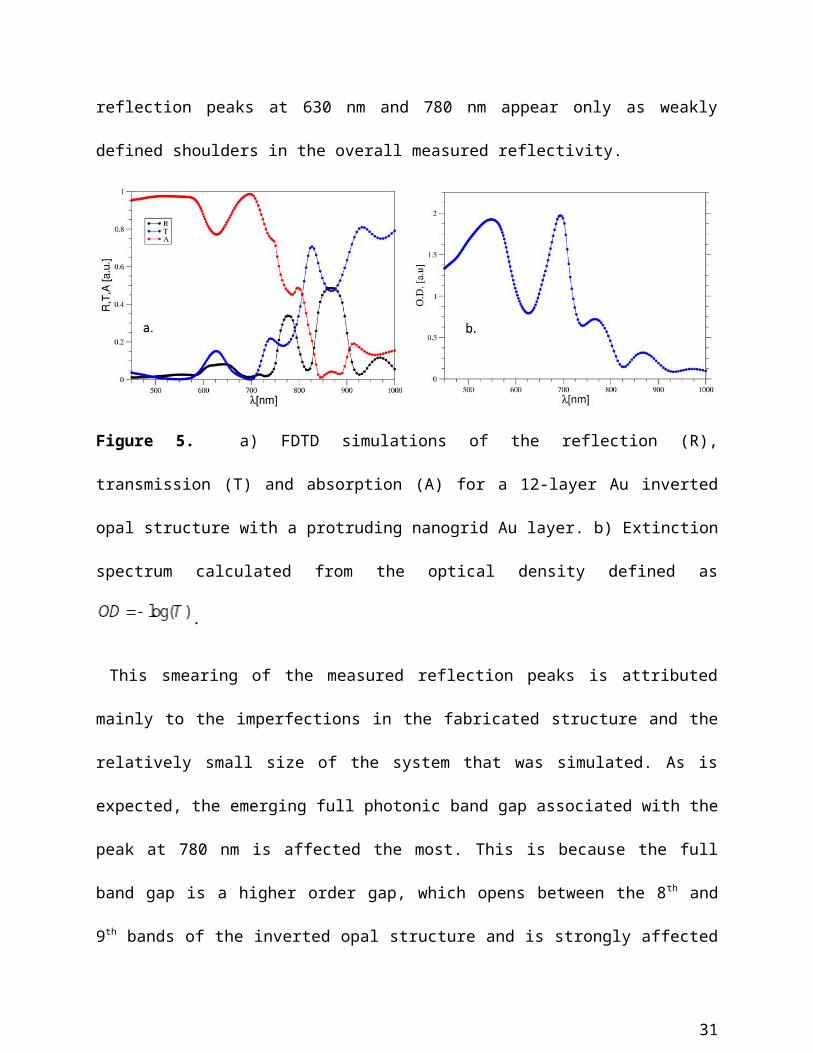
We have performed finite difference time domain (FDTD) simulations, shown in Figure 5, to
explore the plasmonic response of the structure. Figure 5a shows the results for the simulated
reflection, transmission and absorption through the structured nanogrid material. The reflection
spectrum presents a number of peaks associated with the microstructured-Au layer reflectivity
(around 630 nm, which matches the maximum of the effective index of refraction of the Au for
large filling ratios), the emerging full band gap of the Au inverted opal structure (around 780
nm) and the expected -L stop band (870 nm). The reflectivity also shows the characteristic
finite-system oscillations (as the simulated opal structure consists of 12 layers). While the overall
shape and peak position is in good agreement with the measurements in Figure 4e and f, we note
that the predicted reflection peaks at 630 nm and 780 nm appear only as weakly defined
shoulders in the overall measured reflectivity.
19
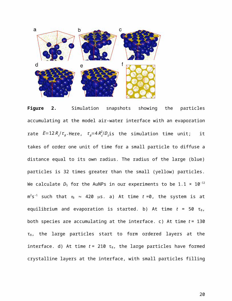
Figure 5. a) FDTD simulations of the reflection (R), transmission (T) and absorption (A) for a
12-layer Au inverted opal structure with a protruding nanogrid Au layer. b) Extinction spectrum
calculated from the optical density defined as .
This smearing of the measured reflection peaks is attributed mainly to the imperfections in the
fabricated structure and the relatively small size of the system that was simulated. As is
expected, the emerging full photonic band gap associated with the peak at 780 nm is affected the
most. This is because the full band gap is a higher order gap, which opens between the 8 th and 9th
bands of the inverted opal structure and is strongly affected by small scale fluctuations in the
dielectric structure. Our observations are in line with those found for the nanoparticle-based
metallodielectric inverse opals described by Wang et al..39
The absorption spectrum presents a broad peak in the lower part of the spectrum induced by
the hybridized NP resonances and bulk Au absorption, and a second major peak at around 700
nm. The origin of the second peak is related to a structuring-induced plasmonic relaxation, as is
confirmed by the electric field distributions shown in Figure 6. In this case, the flatness of the
photonics bands associated with the emergent photonic band gap causes a strongly reduced
group velocity.37 The subsequent slow-light effects result in a strong enhancement of the
20

plasmonic absorption, similar to effects found in previous works.37,40 The extinction spectrum in
Figure 5b displays two major peaks at 550 nm and 696 nm. Although it has an overall shape and
peak position similar to the measurement in Figure 4e, the peaks are blue shifted due to the
approximations made when evaluating the effective Au dielectric permittivity.
Figure 6. Simulations of the magnitude squared of the electric field. (a-c) Plots of the field
associated with the left peak at 550 nm in Fig. 5 (b), and (d-f) the fields associated with the right
21
peak at 696 nm, respectively. The fields are plotted at three depths from the surface within the
3D hybrid structure: (a) and (d) at a depth of 30 nm; (b) and (e) at 120 nm; and (c) and (f) at a
depth of 1050 nm.
We have also analyzed the electric field distribution in the Au nanogrid structure. Figure 6
shows the squared magnitude of the electric field at 550 nm and 696 nm for three different
depths inside the structure: 30 nm in the protruding nanogrid above the opal structure, 120 nm
inside the first layer of the inverted opal and 1050 nm at the bottom of the third layer of the
inverted opal. The field distribution for the peak at 550 nm suggests a delocalized mode with the
electric field modulated along the inverted opal structure, which is consistent with the excitations
of the hybridized AuNP resonances throughout the Au fraction. In contrast, the distribution of
the field for 696 nm suggests a strongly localized mode with well-defined hot spots. As the depth
of the observation is increased, the Au filling is reduced and eventually the field becomes more
uniformly distributed inside the Au layers. Furthermore, the tightly localized field for the 696 nm
mode is strongly affected by the structure filling fraction. In the absence of a well-defined,
tightly-packed protruding AuNP layer, it vanishes, which is consistent with the experimental
findings (Figure 1a and 4e). The protruding AuNP nanogrid structure is only found in
experiments using the faster evaporation rates, and it is only these structures that exhibit two
extinction peaks. To conclude, the overall optical response of the structure is determined both by
the nano-engineering of the Au effective dielectric permittivity and the micro-structuring of the
inverted opal structure. Our simulations support the key experimental finding of two extinction
peaks.
Conclusions
22

We have developed a simple and fast method of colloidal self-assembly to fabricate a hybrid
structure of a quasi-2D array of Au nanoparticles on a 3D opal structure. We use a horizontal
deposition process assisted by NIR radiation to achieve the required fast evaporation rates. The
strongest optical extinction, which is associated with the greatest level of order and a protruding
Au nanogrid, arises from the fastest evaporation rates. Langevin dynamics simulations reveal
that, with fast evaporation rates when the particles are swept up by the falling meniscus, the Au
nanoparticles pass through the interstitial spaces of the larger polymer particles. The use of NIR
radiative heating not only leads to very short fabrication times (about seven minutes), but it also
yields unusual optical spectra. With simulations, we trace the double peaks in the measured
extinction spectra to elementary plasmonic resonances compounded by the optical response of
the supporting opal structure. The optical properties can be tuned through the power density of
the NIR radiation used to speed the evaporation rate. Our method overcomes the time limitations
of a conventional horizontal deposition method while being low-cost and possible to apply over
areas greater than several cm2.
Methods
Synthesis of the Particles
In the synthesis of AuNPs all chemicals were purchased from Sigma-Aldrich and used without
additional purification. The well-established Turkevich-method41 was used. 100 mL of a 1mM
NaAuCl4 aqueous solution was brought to the boil, followed by the addition of 5 mL of a pre-
heated trisodium citrate aqueous solution (2 wt. %) under vigorous stirring. After 5 min. the
color of the reaction solution turned to a characteristic red. The stirring was slowed down and the
mixture was boiled for a further 15 min. before cooling to room temperature.
23

To enable the purification of the AuNPs by centrifugation and to increase the stability of the
dispersion against aggregation, the nanoparticles were coated with bis-(p-sulfonatophenyl)
phenyl-phosphine dihydrate dipotassium salt (BSPP) by a ligand exchange reaction.42 To 100 mL
of a dispersion of the original citrate-coated AuNPs, 50 mg of BSPP was added. After stirring for
at least 4 h, the reaction mixture was passed through a 0.45 µm filter (Millipore). A saturated
sodium chloride solution was added to the AuNPs dispersion until the color changed from red to
blue, indicating the formation of aggregates. The dispersion of the aggregates was centrifuged
for 10 min. at 5000 rpm. The supernatant, containing the excess BSPP, citrate and sodium
chloride, was discarded. The black precipitate was re-dispersed in 1 mL purified water and
sonicated. The concentration of the final AuNP dispersions was determined using the method by
Haiss et al.43
A dispersion of the acrylic copolymer particles was synthesized at AkzoNobel Decorative
R&D (Slough UK). The particles, composed of a copolymer of methyl methacrylate, butyl
acrylate, and methacrylic acid (in a ratio of 18.3:13.3:1 by weight), were made by semi-
continuous emulsion polymerization using an anionic, ethoxylated alcohol surfactant (Rhodafac
RK500A, Rhodia) with ammonium persulphate as the initiator. In previous work, we reported
the evaporation-driven transport in blends of AuNPs and these polymer particles, in the direction
parallel to the substrate.22
Characterization of the Particles
The true diameter, d, of the AuNPs was determined by transmission electron microscopy
(TEM) with a FEI Technai 12 microscope operated at 80 kV. The true diameter of the acrylic
copolymer particles was determined by scanning electron microscopy (SEM) with a JEOL 7100F
field-emission scanning electron microscope operated at an accelerating voltage of 3 kV. The
24

hydrodynamic diameter, dhyd, was measured by dynamic light scattering using a Malvern ME11
Zetasizer Nano ZS. The same instrument was used to measure the zeta-potential (ζ-potential) of
the particles. The glass transition temperature, Tg, of the dry polymer particles was 37.9 °C
measured by differential scanning calorimetry (Q1000, TA Instruments). The results of the
particle characterization are summarized in Table 1. The values for the true diameter, d, are
always lower than the hydrodynamic diameter, dh, because the latter is related to the effective
size of the diffusing object.
Table 1. Sizes and ζ-potential of the acrylic polymer particles and AuNPs
Composition d (nm) dh (nm) ζ-potential (mV)
Acrylic copolymer 338 ± 5 400 ± 6 - 69 ± 1
Acrylic copolymer 261± 5 307 ± 6 - 68 ± 1
Acrylic copolymer
10 nm AuNPs
147 ± 6
10.4 ± 1
174 ± 1
21.1 ± 1
- 67 ± 1
- 50.4 ± 2
Film preparation and drying
The films were prepared by casting aqueous polymer/AuNP blends with a micropipette on
clean microscope glass coverslips (18 mm 18 mm) or appropriately sized square pieces of a
silicon wafer. In all experiments, the initial film thickness of the wet film, H, was 900 µm and
the initial volume fraction of the solid polymer was 4.4 %, so as to obtain a film with a final
25

thickness of 40 µm. The volume fraction of the AuNPs in the dry films was fixed as 0.32 vol.%
in all experiments. The films were dried under one of three different types of condition: (1)
“rapid drying” through radiation with a near-IR-emitting lamp, (2) “normal drying” at room
temperature and in static air (T = 21 °C, RH = 50%), leading to E= 1.1 ×10⁻⁷ ms-1, and (3) “slow
drying” in a high-humidity atmosphere (T = 23°C, RH typically > 95%), leading to E= 3.2 ×10⁻⁹
ms-1.
A chamber, made of acrylic sheets, was used to create the high humidity environment. A
beaker filled with water on a hot-plate (at 40°C) was placed inside the box in order to create a
high-humidity atmosphere. A small rotary fan was placed beneath the ceiling of the box to
prevent condensation of water. With this set-up, an atmosphere with a relative humidity of >
95% was created inside the chamber, resulting in a film drying time of six days. To measure the
evaporation rate of water, a digital balance (interfaced with a computer to record data) was used
inside the chamber.
NIR radiation-assisted drying and evaporation rate determination
For fast drying, the wet films were placed beneath a 250 W near IR-radiation emitting lamp
(Model 470 IR, Interhatch). The experimental set-up is shown in Figure S10. The wet films were
placed with a certain distance, dL, from the near-IR lamp on a heat shielded balance and with a
thermocouple inside to record changes in mass and temperature over time. The gravimetric
measurement recorded an evaporation rate, E, in units of mass per unit of time per area of the
film (found from the slope in Figure 7a). An evaporation rate expressed as a velocity, E, is
obtained by dividing E by the density of the liquid water, ρ, (1000 kg m–3) and the surface area,
A, to give E=E/( ρ∙ A ). Figure 7b shows the evaporation rate increasing as the power density of
the infrared radiation, PIR, increases. This parameter was increased by decreasing dL, as is shown
26

in Figure 7c. The Péclet number depends on the Stokes-Einstein (SE) diffusion coefficient, DS,
which, in turn, is a function of the temperature, T, via the SE equation. For the estimation of DS,
an average temperature, Tave, which is defined as the mean of all temperatures obtained at times
between t = 0 and the drying time was used. Tave increases with PIR are shown in Figure 7d. The
dashed line shows the glass transition temperature, Tg, of the polymer particles. Tave is always
higher than Tg, which enables the formation of a hard, cohesive film via particle coalescence.44
dc
ba
27

Figure 7. Infrared-radiation assisted rapid drying and determination of the evaporation rate. a)
Changes in mass and temperature over time for a typical experiment. b) The evaporation rates
increases with PIR. c) In turn, PIR can be adjusted through variation of dL. d) Average
temperature, Tave, increases as a function of PIR. The dashed line indicates the Tg of the polymer
particles.
Characterization of Hybrid Nanogrids
Scanning electron microscopy (SEM) was conducted on a field-emission electron microscope
(JEOL 7100F FE-SEM). All samples were coated by a thin layer of carbon (> 20 nm, in an
Edwards Auto 306 coater) to increase their electrical conductivity. In the standard procedure, the
SEM was operated with an accelerating voltage of 10 kV. When the AuNP concentration on the
film surface was low, the acceleration voltage was reduced to 5 kV in order to prevent charging
effects and damage by the electron beam.
Atomic force microscopy (AFM) images were obtained on an NTEGRA microscope (NT-
MDT) in intermittent contact mode in air, using a silicon cantilever with a spring constant in the
range from 10 to 130 N/m and a nominal resonant frequency of 275 kHz. UV-Vis-NIR
spectroscopy was performed using a commercial spectrometer (Cray 5000, manufactured by
Varian).
Rutherford backscattering spectrometry (RBS) was conducted at the Surrey Ion Beam Centre
using a 2 MV Tandetron accelerator (High Voltage Engineering Europe). A 5.5 MeV 7Li2+-beam
with good depth resolution was used for detailed structure analysis of the surface up to 4 µm
deep. The scan size was more than 1 mm² with a spot size of ca. 10 µm. The particle detector
and X-ray detector were placed at an angle of 163° and 135°, respectively.445 To reduce the RBS
data, the DataFurnace code46 was used with the software NDFv9.5f to fit the data.47
28

Microscopic UV-vis-NIR spectroscopy (transmission and reflection) was performed using the
output power of a 2 W broadband super-continuum laser (Fianium) as a light source. The light
beam was coupled into a subtractive-mode double prism monochromator to select a narrow
wavelength range of a few nm. To focus the output of the wavelength selector on the sample
surface, the light beam was coupled into a near-infrared objective lens (Mitotoyu Plan Apo NIR,
100×, N.A. 0.5). The transmitted or reflected beam was collected by photodetectors for the
visible (Si) and near-infrared (InGaAs) ranges. A closed-loop piezo-stage was used to move the
sample through the focused beam in order to obtain a 20 µm × 20 µm 2D transmission or
reflection map of the sample.
Macroscopic UV-vis-NIR spectroscopy was performed using a commercial spectrometer (Cary
5000, manufactured by Varian) with a beam having a 1 mm diameter.
Langevin dynamics simulations
Langevin dynamics simulations used the LAMMPS simulation code48 customized to consider
the downward moving water/air interface by modelling it as a soft wall. The parameters in the
simulations were chosen to agree with the experiment; there were 2×10⁵ particles with a number
ratio NS:NL=212:1 and a size ratio RL:RS=32:1. The contact angle of the particles at the water
surface was taken to be = 75°. Other technical information is provided in the Supporting
Information.
Simulations of Optical Properties of Hybrid Nanogrids
A finite-difference time-domain simulation was implemented using Lumerical Solutions
software (FDTD-solutions) to perform transmission and reflection calculations. The polymer
opal was modelled as a 12-layer FCC lattice of spheres with a refractive index of 1.47, particle
radius of 169 nm and an FCC lattice constant of 478 nm. The structure depth was set to
29

approximately 3600 nm to balance accuracy with computational cost. We used a non-uniform
mesh with a Lumerical-defined mesh quality factor of 8 (maximum), and the Au occupied
regions were meshed separately with a resolution of 1 nm. The protruding nanogrid structure was
constructed by etching down with a triangular layer of closed-packed spheres aligned to the top
layer of polymer spheres through a 40 nm-thick Au layer placed on top of the polymer opal. The
structure is shown in Figure S9.
Supporting Information. Quantitative analysis of the structures in SEM images (particle
spacing and quality factor for ordering); SEM and RBS analysis of normally and slowly-dried
hybrid films; description of Langevin dynamics simulations of structure formation; structure and
optical extinction of hybrids with three different polymer particle sizes; FDTD simulations of the
optical properties of hybrids; diagram showing the experimental set-up for NIR radiative heating.
This material is available free of charge via the Internet at http://pubs.acs.org. The authors
confirm that data underlying the findings are available without restriction. Details of the data and
how to request access are available from the University of Surrey publications
repository: http://epubs.surrey.ac.uk .
Corresponding Author
*Joseph L. Keddie; e-mail: [email protected]
Author Contributions
The manuscript was written through contributions of all authors. All authors have given approval
to the final version of the manuscript.
Funding Sources
30
South East Physics Network (SEPNet); EC Seventh Framework Programme (FP7) BARRIER-
PLUS project (number 304758 (FP7-SME-2012-2)); EPSRC (United Kingdom) DTG Grant No.
EP/K503186/1, and EPSRC (United Kingdom) Strategic Equipment Grant No. EP/M008576/1.
31

ACKNOWLEDGMENTS
Funding for the PhD studentship of A.U. and for a summer internship for R.T. was provided
by the South East Physics Network (SEPNet). Funding for A.F. was provided by the EC
BARRIER-PLUS project (number 304758 (FP7-SME-2012-2)). This work was partially
supported by the University of Surrey’s FRSF, Santander and IAA awards to M.F., the EPSRC
(United Kingdom) DTG Grant No. EP/K503186/1, and EPSRC (United Kingdom) Strategic
Equipment Grant No. EP/M008576/1. We thank Mrs. Violeta Doukova and Mr. Chris Burt
(University of Surrey) for technical assistance and Martin Murray and Phil Beharrell (Akzo
Nobel, Slough) for helpful discussions. We are grateful to Akzo Nobel for the donation of the
polymer colloids.
REFERENCES
1. Linn, N. C.; Sun, C.-H.; Jiang, P.; Jiang, B. Self-Assembled Biomimetic Antireflection
Coatings. Appl. Phys. Lett. 2007, 91, 101108.
2. Zhang, X.-T.; Sato, O.; Taguchi, M.; Einaga, Y.; Murakami, T.; Fujishima, A. Self-
Cleaning Particle Coating with Antireflection Properties. Chem. Mater. 2005, 17, 696–700.
3. Anker, J. N.; Hall, W.P.; Lyandres, O.; Shah, N.C.; Zhao J.; Van Duyne, R.P. Biosensing
with Plasmonic Nanosensors. Nat. Mater. 2008, 7, 442–453.
4. Khanadeev, V. A.; Khlebstov, B. N.; Klimova, S. A.; Tsvetkov, M. Y.; Bagratashvili, V.
N.; Sukhorukov, G. B.; Khlebtsov, N.G. Large-Scale High-Quality 2D Silica Crystals: Dip-
Drawing Formation and Decoration with Gold Nanorods and Nanospheres for SERS Analysis.
Nanotechnology 2015, 25, 405602.
32

5. Stebe, K. J.; Lewandowski, E.; Ghosh, M. Oriented Assembly of Metamaterials. Science
2009, 325, 159–160.
6. Atwater, H. A.; Polman, A. Plasmonics for Improved Photovoltaic Devices. Nat. Mater.
2010, 9, 205–213.
7. Cong, H.; Yu, B.; Tang, J.; Li, Z.; Liu, X. Current Status and Future Developments in
Preparation and Application of Colloidal Crystals. Chem. Soc. Rev. 2013, 42, 7774–7800.
8. Wong, S.; Kitaev, V.; Ozin, G. A. Colloidal Crystal Films: Advances in Universality and
Perfection. J. Am. Chem. Soc. 2003, 125, 15589–15598.
9. Yan, Q.; Zhou, Z.; Zhao, X. S. Inward-Growing Self-Assembly of Colloidal Crystal
Films on Horizontal Substrates. Langmuir 2005, 21, 3158–3164.
10. Chung, Y.-W.; Leu, I.-C.; Lee, J.-H.; Hon, M.-H. Influence of Humidity on the
Fabrication of High-Quality Colloidal Crystals Via a Capillary-Enhanced Process. Langmuir
2006, 22, 6454–6460.
11. Zheng, Z.; Liu, X.; Luo, Y.; Cheng, B.; Zhang, D.; Meng, Q.; Wang, Y. Pressure
Controlled Self-Assembly of High Quality Three-Dimensional Colloidal Photonic Crystals.
Appl. Phys. Lett. 2007, 90, 051910.
12. Cai, Z.; Teng, J.; Yan, Q.; Zhao, X. S. Solvent Effect on the Self-Assembly of Colloidal
Microspheres Via a Horizontal Deposition Method. Colloids Surf., A 2012, 402, 37–44.
13. Han, W.; Lin, Z. Learning from “Coffee Rings”: Ordered Structures Enabled by
Controlled Evaporative Self-Assembly. Angew. Chem. Int. Ed. 2012, 51, 1534–1546.
33

14. Vogel, N.; de Viguerie, L.; Jonas, U.; Weiss, C. K.; Landfester, K. Wafer-Scale
Fabrication of Ordered Binary Colloidal Monolayers with Adjustable Stoichiometries. Adv.
Funct. Mater. 2001, 21, 3064–3073.
15. Yan, Q.; Yu, J.; Cai, Z.; Zhao, X. S. Hierarchically Structured Porous Materials: From
Nanoscience to Catalysis, Separation, Optics, Energy, and Life Science. (ed. B.-L- Su, C.
Sanchez and X. Yang, Wiley-VCH, Weinheim, 2012).
16. Reyes, Y.; Duda, Y. Modeling of Drying in Films of Colloidal Particles. Langmuir 2005,
21, 7057–7060.
17. Jang, H. Y.; Lee, S.-K.; Cho, S. H.; Ahn, J.-H.; Park, S. Fabrication of Metallic
Nanomesh: Pt Nano-Mesh as a Proof of Concept for Stretchable and Transparent Electrodes.
Chem. Mater. 2013, 25, 3535–3538.
18. Li, C.; Hong, G.; Qi, L. Nanosphere Lithography at the Gas/Liquid Interface: A General
Approach toward Free-Standing High-Quality Nanonets. Chem. Mater. 2010, 22, 476–481.
19. Bartlett, P. N.; Birkin, P. R.; Ghanem, M. A. Electrochemical Deposition of Macroporous
Platinum, Palladium and Cobalt Films Using Polystyrene Latex Sphere Templates. Chem.
Commun. 2000, 17, 1671–1672.
20. Romanov, S. G.; Korovin, A. V.; Regensburger, A.; Peschel, U. Hybrid Colloidal
Plasmonic-Photonic Crystals. Adv. Mater. 2011, 23, 2515–2533.
21. Boriskina, S. V.; Povinelli, M.; Astratov, V. N.; Zayats, A. V.; Podolskiy, V. A.
Collective Phenomena in Photonic, Plasmonic and Hybrid structures. Opt. Express 2011, 19,
22024–22028.
34

22. Utgenannt, A.; Keddie, J.L.; Muskens, O.L.; Kanaras, A.G. Directed Organization
of Gold Nanoparticles in Polymer Coatings through Infrared-Assisted Evaporative Lithography.
Chem. Commun. 2013, 49, 4253-4255.
23. Scheeler, S. P.; Mühlig, S.; Rockstuhl, C.; Bin Hasan, S.; Ullrich, S.; Neubrech, F.;
Kudera, S.; Pacholski, C. Plasmon Coupling in Self-Assembled Gold Nanoparticle-Based
Honeycomb Islands. J. Phys. Chem. C 2013, 117, 18634–18641.
24. Cintra, S.; Abdelsalam, M. E.; Bartlett, P. N.; Baumberg, J.J.; Kelf, T. A.; Sugawara, Y.;
Russell, A. E. Sculpted Substrates for SERS. Faraday Discuss. 2006, 132, 191–199.
25. Routh, A. F.; Zimmerman, W. B. Distribution of Particles during Solvent Evaporation
from Films. Chem. Eng. Sci. 2004, 59, 2961–2968.
26. Trueman, R. E.; Lago Domingues, E.; Emmett, S. N.; Murray, M. W.; Routh, A. F. Auto-
Stratification in Drying Colloidal Dispersions: A Diffusive Model. J. Colloid Interface Sci. 2012,
377, 207–212.
27. Cardinal, C. M.; Jung, Y. D.; Ahn, K. H.; Francis, L. F. Drying Regime Maps for
Particulate Coatings. AIChE J. 2010, 56, 2769–2780.
28. Romanov, S. G.; Susha, A. S.; Sotomayor Torres, C. M.; Liang, Z.; Caruso, F. Surface
Plasmon Resonance in Gold Nanoparticle Infiltrated Dielectric Opals. J. Appl. Phys. 2005, 97,
086103.
29. Morandi, V.; Marabelli, F.; Amendola, V.; Meneghetti, M.; Comoretto, D. Colloidal
Photonic Crystals Doped with Gold Nanoparticles: Spectroscopy and Optical Switching
Properties. Adv. Funct. Mater. 2007, 17, 2779–2786.
35

30. Wang, D.; Li, J.; Chan, C. T.; Salgueirico-Maceira, V.; Liz-Marzan, L. M.; Romanov, S.;
Caruso, F. Optical Properties of Nanoparticle-Based Metallodielectric Inverse Opals. Small
2005, 1, 122-130.
31. Halas, N. J.; Lal, S.; Chang, W.-S.; Link, S.; Nordlander, P. Plasmons in Strongly Coupled
Metallic Nanostructures. Chem. Rev. 2011, 111, 3913– 3961.
32. Zhong, Z.; Patskovskyy, S.; Bouvrette, P.; Luong, J. H. T.; Gedanken, A. The Surface
Chemistry of Au Colloids and Their Interactions with Functional Amino Acids. J. Phys. Chem.
B 2004, 108, 4046– 4052.
33. Barrow, S. J.; Wei, X.; Baldauf, J. S.; Funston, A. M.; Mulvaney, P. The Surface Plasmon
Modes of Self-Assembled Gold Nanocrystals. Nat. Commun. 2012, 3, 1275.
34. Kelf, T. A.; Sugawara, Y.; Cole, R. M.; Baumberg, J. J.; Abdelsalam, M. E.; Cintra, S.;
Mahajan, S.; Russell, A. E.; Bartlett, P. N. Localized and Delocalized Plasmons in Metallic
Nanovoids. Phys. Rev. B 2006, 74, 245415.
35. Lin, T.-L.; Lin, J.-H.; Guo, J.-T.; Kan, H.-C. Suppression of Photonic Bandgap Reflection
by Localized Surface Plasmons in Self-Assembled Plasmonic–Photonic Crystals, Adv. Opt.
Mater. 2015, 3, 1470-1475.
36. Robbiano, V.; Giordano, M.; Martella, C; Di Stasio, F.; Chiappe, D.; Buatier de Mongeot, F.;
Comoretto, D. Hybrid Plasmonic–Photonic Nanostructures: Gold Nanocrescents Over Opals,
Adv. Opt. Mater. 2013, 1, 389-396.
37. Morandi, V.; Marabelli, F.; Amendola, V.; Meneghetti, M.; Comoretto, D. Light Localization
Effect on the Optical Properties of Opals Doped with Gold Nanoparticles, J. Phys. Chem. C
2008, 112, 6293-6298.
36

38. Bahns, J. T.; Guo, Q.; Montgomery, J. M.; Gray, S. K.; Jaeger, H. M.; Chen, L. High-Fidelity
Nano-Hole-Enhanced Raman Spectroscopy. J. Phys. Chem. C 2009, 113, 11190-11197.
39. Sánchez-Sobrado, O.; Lozano, G.; Calvo, M. E.; Sánchez-Iglesias, A.; Liz-Marzán, L. M.;
Míguez, H. Interplay of Resonant Cavity Modes with Localized Surface Plasmons: Optical
Absorption Properties of Bragg Stacks Integrating Gold Nanoparticles, Adv. Mater. 2011, 23,
2108–2112.
40. Yoo, S; Park, Q-H. Effective Permittivity for Resonant Plasmonic Nanoparticle Systems Via
Dressed Polarizability. Opt. Express 2012, 20, 16480–16489.
41. Turkevich, J.; Stevenson, P. C.; Hillier, J. A Study of the Nucleation and Growth Process in
the Synthesis of Colloidal Gold. Discuss. Faraday Soc. 1951, 11, 55–75.
42. Loweth, C. J.; Caldwell, W. B.; Peng, X.; Alivisatos, A. P.; Schultz, P. G. DNA-Based
Assembly of Gold Nanocrystals. Angew. Chem. Int. Ed. 1999, 5, 1808–1812.
43. Haiss, W.; Thanh, N. T. K.; Aveyard, J.; Fernig, D. G. Determination of Size and
Concentration of Gold Nanoparticles from UV-Vis Spectra. Anal. Chem. 2007, 79, 4215–4221.
44. Georgiadis, A.; Bryant, P. A.; Murray, M.; Beharrell, P.; Keddie, J. L. Resolving the Film
Formation Dilemma with Infrared Radiation-Assisted Sintering. Langmuir 2011, 27, 2176–2180.
45. Simon, A.; Jeynes, C.; Webb, R. P.; Finnis, R.; Tabatabaian, Z.; Sellin, P. J.; Breese, M. B.
H.; Fellows, D. F.; van den Broek, R.; Gwilliam, R. M. The New Surrey Ion Beam Analysis
Facility. Nucl. Instruments Methods Phys. Res. Sect. B Beam Interact. with Mater. Atoms 2004,
219-220, 405–409.
46. Jeynes, C.; Bailey, M. J.; Bright, N.J.; Christopher, M. E.; Grime, G. W.; Jones, B. N.;
Palitsin, V. V.; Webb, R. P. “Total IBA” – Where Are We? Nucl. Instrum. Methods Phys. Res.
Sect. B 2012, 271, 107–118.
37

47. Barradas, N. P.; Jeynes, C. Advanced Physics and Algorithms in the IBA DataFurnace. Nucl.
Instrum. Methods Phys. Res. Sect. B, 2008, 266, 1875–1879.
48. Plimpton, S. Fast Parallel Algorithms for Short-Range Molecular Dynamics. J. Comp. Phys.
1995, 117, 1-19.
38

Table of Contents Graphic
39