Embed Size (px)
Citation preview
High-Speed Directly Modulated Heterogeneously Integrated InP/Si DFB Laser
G. Morthier(1,2), A. Abbasi(1,2), J. Verbist(1,2,3), S. Keyvaninia(1,2), X. Yin(2,3), F. Lelarge(4), G-H Duan(4), J. Bauwelinck(2,3), G. Roelkens(1,2)
(1) Photonics Research Group, INTEC, Ghent University-IMEC, Belgium, [email protected] (2) Center for Nano- and Biophotonics, Ghent University, Belgium (3) Design-IBCN Group, INTEC, Ghent University – iMinds – IMEC, 9000 Ghent, Belgium (4) III-V lab, a joint lab of 'Alcatel-Lucent Bell Labs France', 'Thales Research and Technology' and
'CEA Leti'
Abstract We discuss how InP membrane laser diodes, heterogeneously integrated on SOI can be
designed for high speed operation. This is illustrated with several static and dynamic characteristics of
fabricated lasers. We finally report link experiments with the directly modulated lasers.
Introduction
There is a growing need for high bitrate
interconnects, a.o. for intra data center and inter
data center interconnects. Standards for 400
GbE are emerging and some companies have
even expressed interest in a Terabit Ethernet
standard1. It is expected that 400 GbE will be
based on lane speeds of 25 Gb/s, 50 Gb/s and
even 100 Gb/s. Especially for distances of more
than 10 km, there is great interest in using either
8 wavelengths, each carrying 50 Gb/s NRZ-OOK,
and 4 wavelengths each carrying 100 Gb/s PAM-
4 modulation2.
In the past years many external modulators (both
electro-absorption and Mach-Zehnder) have
been reported with maximum bitrates of 56 Gb/s
or more3,4. However, also several DFB laser
diodes and VCSELs have been reported at 1300
and 1550 nm that are capable of direct
modulation up to 56 Gb/s5,6. External modulation
is more power consuming than direct
modulation7, results in extra footprint and comes
with insertion loss. VCSELs on the other hand are
difficult to integrate into a WDM transmitter and
may not give enough output power for longer
reach links. DFB lasers are much better suited for
photonic integration and easily give the required
output powers for longer distance interconnects.
In the past years, we have been working on
directly modulated InP DFB membrane lasers,
heterogeneously integrated onto silicon on
insulator (SOI) and we’ll discuss the progress in
that area below. The fabrication on SOI brings a
number of potential advantages. Since SOI is
very well suited for the implementation of
compact, passive optical components, it is
straightforward to integrate arrays of
heterogeneously integrated lasers with
components such as optical filters or
multiplexers. The laser diodes are in principle
also more suited for co-integration with driver
electronics implemented in BiCMOS8. The
shorter electrical connections would then allow to
avoid impedance controlled interconnects,
resulting in lower power consumption and larger
electrical bandwidth. Finally, the development of
transfer printing techniques make the
heterogeneous integration possible with efficient
use of the III-V material9.
Design and fabrication
The laser diodes are realised by integrating the
III-V epitaxial structure on top of the SOI
waveguides using adhesive bonding and
subsequent processing 10. Coupling between the
InP mesa and the 400nm thick silicon
waveguides is obtained by adiabatic tapering of
both the InP mesa and the Si waveguides10. The
Bragg grating is realised in the underlying Si
waveguides with an etch of 180nm deep. The
bonding layer thickness and InP mesa structure
are designed such that the mode has a good
overlap with the active layer and the grating. A
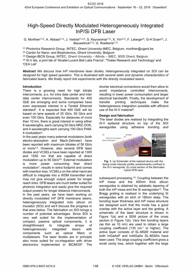
schematic of the laser structure is shown in
Figure 1(a) and a SEM picture of the cross
section in Figure 1(b). Very thin bonding layers
(as thin as 10 nm) are used to obtain a large
coupling coefficient (135 cm-1 or higher). The
active layer consists of SL-MQW material and
both InGaAsP and InAlGaAs SL-MQWs have
been used. The large coupling coefficient gives a
small cavity loss, which together with the large
Fig. 1: (a) Schematic of the realized device with the lasing mode intensity profile, predominantly confined in the III-V waveguide; (b) cross section of the fabricated
hybrid DFB laser
148
ECOC 2016 42nd European Conference and Exhibition on Optical Communications ∙ September 18 – 22, 2016 ∙ Düsseldorf
ISBN 978-3-8007-4274-5 © VDE VERLAG GMBH ∙ Berlin ∙ Offenbach
confinement factor for the active layer results in a
small threshold gain and a large differential gain.
The laser light is coupled from the Si waveguide
to single mode fiber using surface grating
couplers.
The implementation of the grating in an
underlying Si waveguide implies that the lasing
mode has to overlap well with both the active
layer and the Si waveguide. This compromises
the confinement factor (and thus the resonance
frequency) somewhat compared to membrane
lasers which are bonded on SiO2/Si substrates11,
but makes the fabrication easier. The tapers
required for the coupling between the InP
membrane and the Si waveguide were so far
always pumped and modulated together with the
DFB section. It is however expected that better
modulation behaviour can be achieved when the
taper currents are not modulated and results for
modulation of the DFB current only will be
discussed at the conference.
Results from InGaAsP MQW lasers
The first batch of high speed lasers were
fabricated using a III-V layer stack consisting of 6
InGaAsP quantum wells (photoluminescence
peak at 1.55 µm) sandwiched between InGaAsP
separate confinement heterostructure layers
(bandgap wavelength 1.17 µm) and InP cladding
layers. The total thickness of the bonding layer
(BCB and oxide) is 50 nm. This results in lasers
with typical threshold current below 20 mA, a
power in the Si waveguide of 6 mW at 100 mA
and SMSR of 45 dB at a stage temperature of
20 C̊. The current is injected into both the laser
(above the grating) and the tapers, which act as
semiconductor optical amplifer (SOA). The length
of the laser is 340 m and that of the tapers is
220 m. From the width of the stopband, a
coupling coefficient of 135 cm-1 was estimated.
This laser showed a 3dB small signal modulation
bandwidth of 15 GHz at a 100 mA bias current.
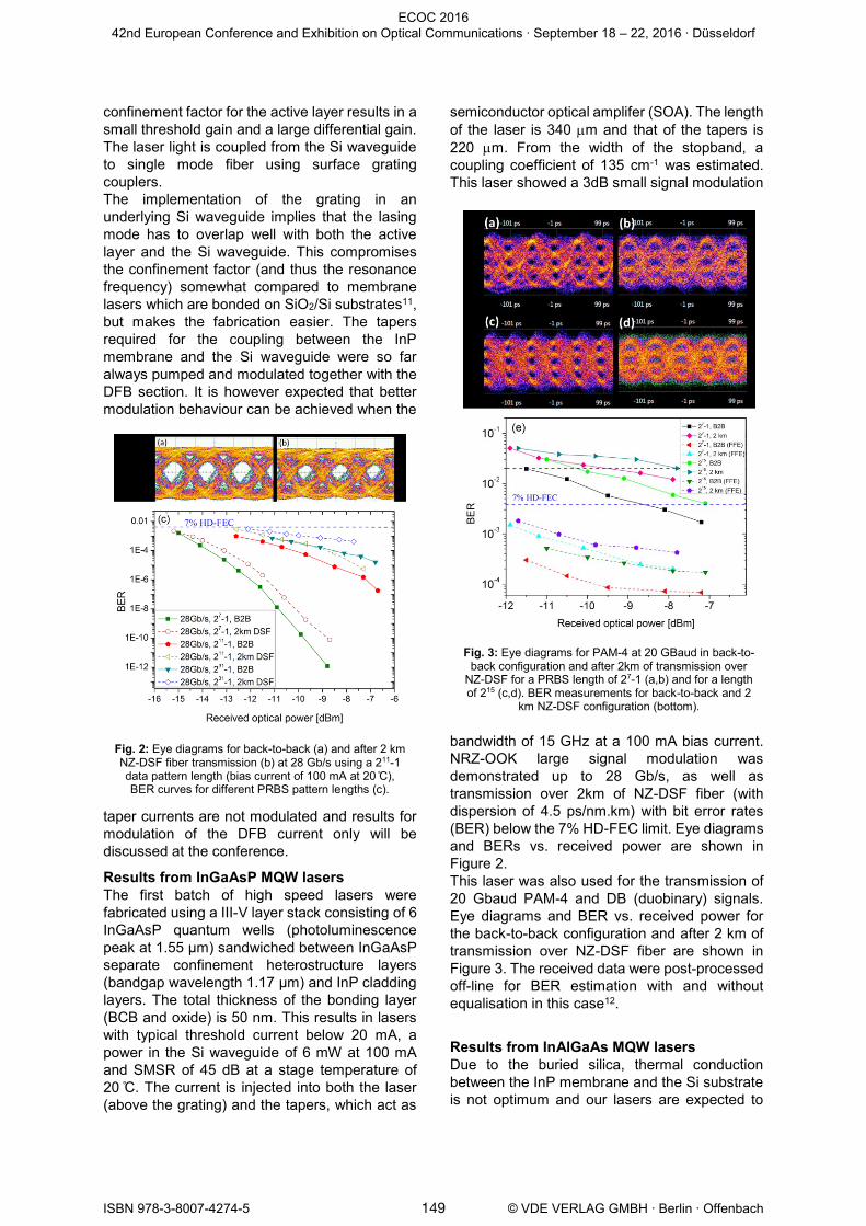
NRZ-OOK large signal modulation was
demonstrated up to 28 Gb/s, as well as
transmission over 2km of NZ-DSF fiber (with
dispersion of 4.5 ps/nm.km) with bit error rates
(BER) below the 7% HD-FEC limit. Eye diagrams
and BERs vs. received power are shown in
Figure 2.
This laser was also used for the transmission of
20 Gbaud PAM-4 and DB (duobinary) signals.
Eye diagrams and BER vs. received power for
the back-to-back configuration and after 2 km of
transmission over NZ-DSF fiber are shown in
Figure 3. The received data were post-processed
off-line for BER estimation with and without
equalisation in this case12.
Results from InAlGaAs MQW lasers
Due to the buried silica, thermal conduction
between the InP membrane and the Si substrate
is not optimum and our lasers are expected to
Fig. 2: Eye diagrams for back-to-back (a) and after 2 km NZ-DSF fiber transmission (b) at 28 Gb/s using a 211-1 data pattern length (bias current of 100 mA at 20 ̊C), BER curves for different PRBS pattern lengths (c).
Fig. 3: Eye diagrams for PAM-4 at 20 GBaud in back-to-back configuration and after 2km of transmission over
NZ-DSF for a PRBS length of 27-1 (a,b) and for a length of 215 (c,d). BER measurements for back-to-back and 2
km NZ-DSF configuration (bottom).
149
ECOC 2016 42nd European Conference and Exhibition on Optical Communications ∙ September 18 – 22, 2016 ∙ Düsseldorf
ISBN 978-3-8007-4274-5 © VDE VERLAG GMBH ∙ Berlin ∙ Offenbach
have relatively strong internal heating. As
InAGaAs active layers suffer less from high
temperatures, we have recently moved to Al-
containing active layers with SL-MQWs. The first
lasers have been fabricated and first results have
been obtained on the modulation.
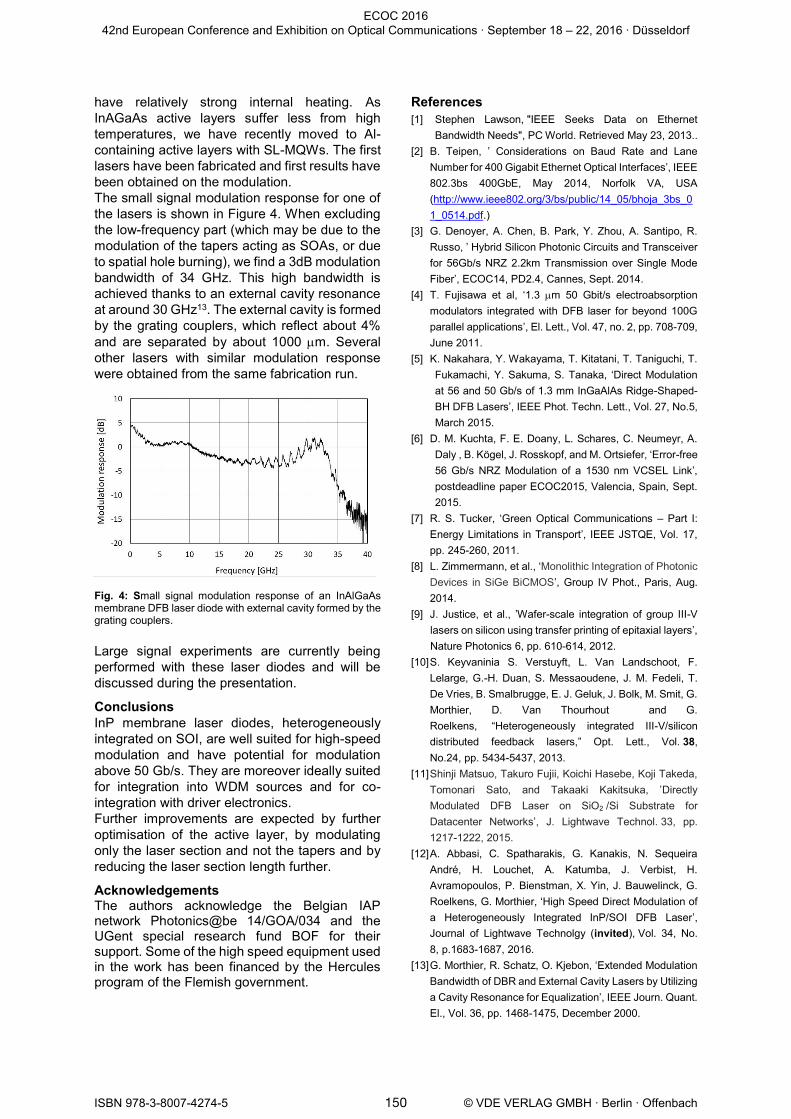
The small signal modulation response for one of
the lasers is shown in Figure 4. When excluding
the low-frequency part (which may be due to the
modulation of the tapers acting as SOAs, or due
to spatial hole burning), we find a 3dB modulation
bandwidth of 34 GHz. This high bandwidth is
achieved thanks to an external cavity resonance
at around 30 GHz13. The external cavity is formed
by the grating couplers, which reflect about 4%
and are separated by about 1000 m. Several
other lasers with similar modulation response
were obtained from the same fabrication run.
Fig. 4: Small signal modulation response of an InAlGaAs membrane DFB laser diode with external cavity formed by the grating couplers.
Large signal experiments are currently being
performed with these laser diodes and will be
discussed during the presentation.
Conclusions
InP membrane laser diodes, heterogeneously
integrated on SOI, are well suited for high-speed
modulation and have potential for modulation
above 50 Gb/s. They are moreover ideally suited
for integration into WDM sources and for co-
integration with driver electronics.
Further improvements are expected by further
optimisation of the active layer, by modulating
only the laser section and not the tapers and by
reducing the laser section length further.
Acknowledgements The authors acknowledge the Belgian IAP network Photonics@be 14/GOA/034 and the UGent special research fund BOF for their support. Some of the high speed equipment used in the work has been financed by the Hercules program of the Flemish government.
References
[1] Stephen Lawson, "IEEE Seeks Data on Ethernet
Bandwidth Needs", PC World. Retrieved May 23, 2013..
[2] B. Teipen, ’ Considerations on Baud Rate and Lane
Number for 400 Gigabit Ethernet Optical Interfaces’, IEEE
802.3bs 400GbE, May 2014, Norfolk VA, USA
(http://www.ieee802.org/3/bs/public/14_05/bhoja_3bs_0
1_0514.pdf.)
[3] G. Denoyer, A. Chen, B. Park, Y. Zhou, A. Santipo, R.
Russo, ’ Hybrid Silicon Photonic Circuits and Transceiver
for 56Gb/s NRZ 2.2km Transmission over Single Mode
Fiber’, ECOC14, PD2.4, Cannes, Sept. 2014.
[4] T. Fujisawa et al, ‘1.3 m 50 Gbit/s electroabsorption
modulators integrated with DFB laser for beyond 100G
parallel applications’, El. Lett., Vol. 47, no. 2, pp. 708-709,
June 2011.
[5] K. Nakahara, Y. Wakayama, T. Kitatani, T. Taniguchi, T.
Fukamachi, Y. Sakuma, S. Tanaka, ‘Direct Modulation
at 56 and 50 Gb/s of 1.3 mm InGaAlAs Ridge-Shaped-
BH DFB Lasers’, IEEE Phot. Techn. Lett., Vol. 27, No.5,
March 2015.
[6] D. M. Kuchta, F. E. Doany, L. Schares, C. Neumeyr, A.
Daly , B. Kögel, J. Rosskopf, and M. Ortsiefer, ‘Error-free
56 Gb/s NRZ Modulation of a 1530 nm VCSEL Link’,
postdeadline paper ECOC2015, Valencia, Spain, Sept.
2015.
[7] R. S. Tucker, ‘Green Optical Communications – Part I:
Energy Limitations in Transport’, IEEE JSTQE, Vol. 17,
pp. 245-260, 2011.
[8] L. Zimmermann, et al., ‘Monolithic Integration of Photonic
Devices in SiGe BiCMOS’, Group IV Phot., Paris, Aug.
2014.
[9] J. Justice, et al., ’Wafer-scale integration of group III-V
lasers on silicon using transfer printing of epitaxial layers’,
Nature Photonics 6, pp. 610-614, 2012. [10] S. Keyvaninia S. Verstuyft, L. Van Landschoot, F.
Lelarge, G.-H. Duan, S. Messaoudene, J. M. Fedeli, T.
De Vries, B. Smalbrugge, E. J. Geluk, J. Bolk, M. Smit, G.
Morthier, D. Van Thourhout and G.
Roelkens, “Heterogeneously integrated III-V/silicon
distributed feedback lasers,” Opt. Lett., Vol. 38,
No.24, pp. 5434-5437, 2013.
[11] Shinji Matsuo, Takuro Fujii, Koichi Hasebe, Koji Takeda,
Tomonari Sato, and Takaaki Kakitsuka, ’Directly
Modulated DFB Laser on SiO2 /Si Substrate for
Datacenter Networks’, J. Lightwave Technol. 33, pp.
1217-1222, 2015.
[12] A. Abbasi, C. Spatharakis, G. Kanakis, N. Sequeira
André, H. Louchet, A. Katumba, J. Verbist, H.
Avramopoulos, P. Bienstman, X. Yin, J. Bauwelinck, G.
Roelkens, G. Morthier, ‘High Speed Direct Modulation of
a Heterogeneously Integrated InP/SOI DFB Laser’,
Journal of Lightwave Technolgy (invited), Vol. 34, No.
8, p.1683-1687, 2016.
[13] G. Morthier, R. Schatz, O. Kjebon, ‘Extended Modulation
Bandwidth of DBR and External Cavity Lasers by Utilizing
a Cavity Resonance for Equalization’, IEEE Journ. Quant.
El., Vol. 36, pp. 1468-1475, December 2000.
150
ECOC 2016 42nd European Conference and Exhibition on Optical Communications ∙ September 18 – 22, 2016 ∙ Düsseldorf
ISBN 978-3-8007-4274-5 © VDE VERLAG GMBH ∙ Berlin ∙ Offenbach