Embed Size (px)
Citation preview
100
Temperature Effects on the Electrical Characteristics of BJTs and MOSFETs
Reiham. O. Ibrahim*1, S. M. Abd El-Azeem
1, S. M. El-Ghanam
1 and F. A. S.Soliman
2
1- Electronic Res. Lab., Physics Dept., Faculty of Women for Arts,
Science and Education, Ain-Shams Univ., Cairo, Egypt.
2- Nuclear Materials Authority, P. O. Box 530-Maadi-11728, Cairo, Egypt.
*Corresponding author: E-mail address: [email protected]
Abstract
The aim of the present paper is to shed further light on studying the temperature effects on
the static (I-V) and dynamic (C-V) characteristics of bipolar junction- and metal oxide field
effect - transistors. In this concern, several parameters were plotted at different temperature
levels. The experimental results showed that, for the bipolar junction transistor 2SC2120, a
noticeable increase in the collector current and the current gain from 0.198 A and 0.14 up-to
0.25 A and 0.24 by increasing the temperature from 25ºC and 135ºC, respectively. Considering
the threshold voltage, its value was shown to be decreased from 0.62 Volt to 0.42 Volt within
the same temperature range. In addition, from the traced dynamic characteristics of the same
BJT, the diffusion capacitance of the emitter-base junction, as an example, increased from
10.11 nF up-to 45.09 nF by increasing the temperature up-to 135 ºC. On the other hand, for
metal oxide field effect transistor 2N6660, the static characteristics showed that a noticeable
decrease in the drain current and the forward trans-conductance from 1.2A and 5.0 Ω-1
down-to
0.79 A and 1.9 Ω-1
, respectively, due to temperature increasing from 25 ºC up-to 135 ºC. While
the threshold voltage was hold constant. Finally, the reverse capacitance of the gate-drain
junction was shown to be increases from 41.48 pF up-to 47.31 pF within the same range of
temperature.
Keywords: Temperature effect, bipolar junction transistor, metal oxide field effect transistor,
capacitance, impedance, quality and dissipation factor and phase angle.
1.0 Introduction
Temperature is one of the most common keys design factors in electronic designs. Designers
must confirm that semiconductor devices operate correctly across a wide range of temperatures
[T. D. Haeffner, 2015]. Temperature can change the operation of semiconductor devices
significantly. To make the design of some application possible as an example, biomedical
applications, such as breathing sensors, temperature sensors and other applications, the
temperature characteristics of the transistors must be considered [S. Bethi, et al, 2014]. In this
concern, the present paper targets to study the electrical parameters for two of the most
commonly two used electronic devices, namely: NPN bipolar junction Si-transistor (BJT) and N-
channel enhancement mode MOSFET under the influence of different levels of temperature.
101
. 2.0 Experimental Work
The experimental work was based on studying the electrical parameters of NPN (BJT)
type 2SC2120 and N-channel enhancement mode MOSFET type 2N6660 under the influence
of wide temperature levels, ranging from 25 ºC up-to 135 ºC. In this concern, 370 A
Tektronix curve tracer system and programmable automatic Fluke PM6306 RCL bridge were
applied for precise measurements.
3.0. Results and Discussions
3.1. Static Characterization of Transistors
3.1.1. Bipolar junction transistors
The output characteristic curves (collector current IC, collector-emitter voltage VCE, of the Si-
2SC2120 transistor were plotted at base current IB value of 1 mA, under the influence of
different temperature levels, ranging from 25ºC up-to 135ºC Fig. (1). It is clearly shown that, IC
increases as a function of temperature level, where at VCE = 3 Volts, IC reaches a value of 0.25 A,
measured at 135 ºC, while its initial value was 0.198 A, measured at 25 ºC [A. S. Sedra, 2004,
N. Rinaldi and V. Alessandro,2005].
Fig. (1): Dependence of the output characteristics curve on temperature for BJT type 2SC2120.
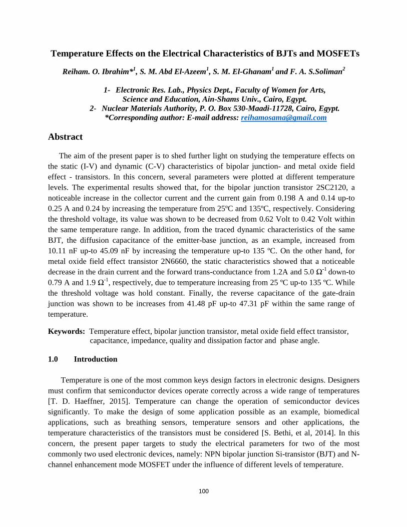
Besides, the output-resistance (Rout) of BJT`s was calculated for the different temperature
levels using Eq. (1) and the dependence of its value on temperature was shown in Fig. (2a) [B.L.
Theraja, 2008, J. Millman and C.C. Halkias, 1972]. From which, it is shown that Rout decreased
from an initial value of 15 Ω, measured at 25 ºC down-to 8.54 Ω, at 135 ºC, after that saturation
conditions was observed.
Rout = ………………………………….. (1)
Where,
∆VCE: Change in collector-emitter voltage and
∆IC: Change in collector current.
0 2 4 6 8 100.00
0.05
0.10
0.15
0.20
0.25
0.30T= 25 75 95 115 135
oC
Colle
cto
r C
urr
ent,
A
Collector-Emitter Voltage, V
IB
= 1mA
C
CE
I
V
102
Also, dc current gain (hFE) was calculated applying Eq. (2) and plotted as function of
temperature Fig. (2b) [A. S. Sedra, 2004, B.L. Theraja, 2008 and J. Millman and C.C. Halkias,
1972]. From which, it is clear that, hFE increased from an initial value of 0.14, measured at 25 ºC
up-to 0.239, at 135 ºC, and at the end, saturation conditions was observed.
hFE = B
C
I
I
………………………………………………. (2)
Where;
∆IC: Change in collector current and
∆IB: Change in base current
(a) (b)
Fig. (2): Temperature dependence of the dc current gain (a) and output-resistance (b) of BJT
type 2SC2120.
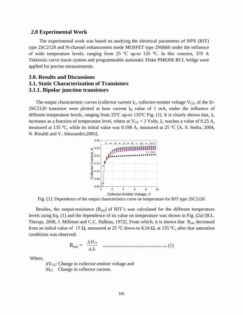
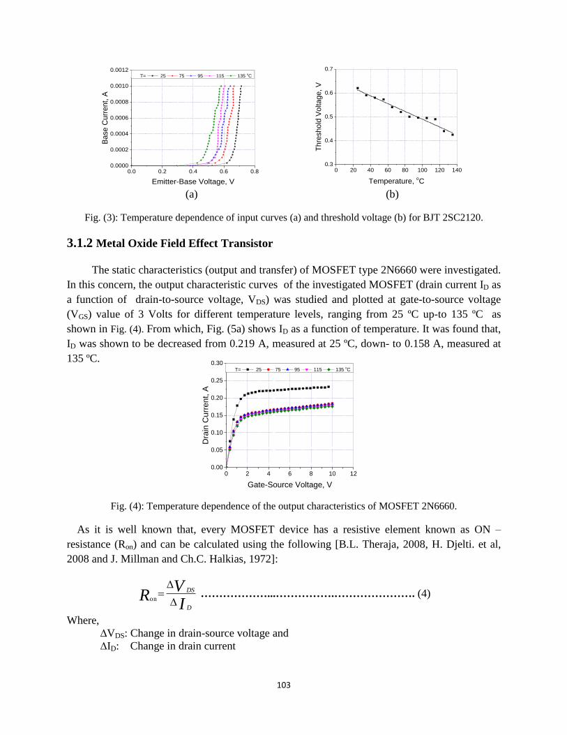
In addition, the study was extended to include the temperature effect on the input
characteristics of the investigated transistor. Where, Fig. (3a) shows a set of (IB-VBE) curves
plotted within the temperature range from 25 ºC up-to 135 ºC. As a result, the dependence of the
threshold voltage (VTh) on temperature was shown in Fig. (3b). From which, VTh value was
shown to be decreased from 0.62 Volt down-to 0.42 Volt, in the temperature range from 25oC
up-to 135 oC, this is mainly due to the fact that the increasing temperature leads the electrons in
the valance band to be excited, pulling them into the conduction band, resulting an increase in
the current. The temperature dependence was shown to be linear decay, following the relation
[B. Eslamia and S. Ashrafib, 2016, E. Schurackm, et al, 1992 and Yam Agiwa, et al, 2008]:
ATVTV ThTh 0 …………………..…………….... (3)
Where;
VTh(T) and VTh (0): threshold voltages (Cut-in voltage), measured at measuring-and
room-temperature level, respectively.
A: slope of the dependence, and
T: temperature
0 20 40 60 80 100 120 1400.10
0.15
0.20
0.25
0.30
hF
E
Temperature, oC
0 20 40 60 80 100 120 1406
8
10
12
14
16
O
ut-
Re
sis
tan
ce,
Temperature, oC
103
(a) (b)
Fig. (3): Temperature dependence of input curves (a) and threshold voltage (b) for BJT 2SC2120.
3.1.2 Metal Oxide Field Effect Transistor
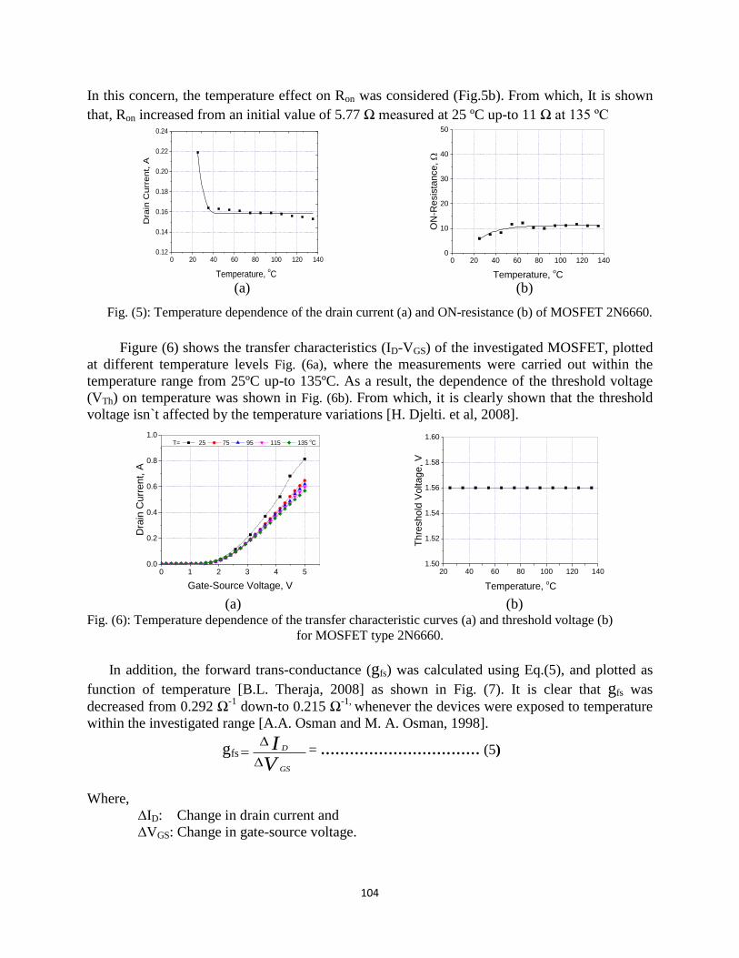
The static characteristics (output and transfer) of MOSFET type 2N6660 were investigated.
In this concern, the output characteristic curves of the investigated MOSFET (drain current ID as
a function of drain-to-source voltage, VDS) was studied and plotted at gate-to-source voltage
(VGS) value of 3 Volts for different temperature levels, ranging from 25 ºC up-to 135 ºC as
shown in Fig. (4). From which, Fig. (5a) shows ID as a function of temperature. It was found that,
ID was shown to be decreased from 0.219 A, measured at 25 ºC, down- to 0.158 A, measured at
135 ºC.
Fig. (4): Temperature dependence of the output characteristics of MOSFET 2N6660.
As it is well known that, every MOSFET device has a resistive element known as ON –
resistance (Ron) and can be calculated using the following [B.L. Theraja, 2008, H. Djelti. et al,
2008 and J. Millman and Ch.C. Halkias, 1972]:
IV
RD
DS
on ………………...…………….…………………. (4)
Where,
∆VDS: Change in drain-source voltage and
∆ID: Change in drain current
0.0 0.2 0.4 0.6 0.80.0000
0.0002
0.0004
0.0006
0.0008
0.0010
0.0012T= 25 75 95 115 135
oC
Ba
se
Cu
rre
nt, A
Emitter-Base Voltage, V
0 2 4 6 8 10 120.00
0.05
0.10
0.15
0.20
0.25
0.30T= 25 75 95 115 135
oC
Dra
in C
urr
ent, A
Gate-Source Voltage, V
0 20 40 60 80 100 120 1400.3
0.4
0.5
0.6
0.7
Thre
shold
Voltage, V
Temperature, oC
104
In this concern, the temperature effect on Ron was considered (Fig.5b). From which, It is shown
that, Ron increased from an initial value of 5.77 Ω measured at 25 ºC up-to 11 Ω at 135 ºC
(a) (b)
Fig. (5): Temperature dependence of the drain current (a) and ON-resistance (b) of MOSFET 2N6660.
Figure (6) shows the transfer characteristics (ID-VGS) of the investigated MOSFET, plotted
at different temperature levels Fig. (6a), where the measurements were carried out within the
temperature range from 25ºC up-to 135ºC. As a result, the dependence of the threshold voltage
(VTh) on temperature was shown in Fig. (6b). From which, it is clearly shown that the threshold
voltage isn`t affected by the temperature variations [H. Djelti. et al, 2008].
(a) (b) Fig. (6): Temperature dependence of the transfer characteristic curves (a) and threshold voltage (b)
for MOSFET type 2N6660.
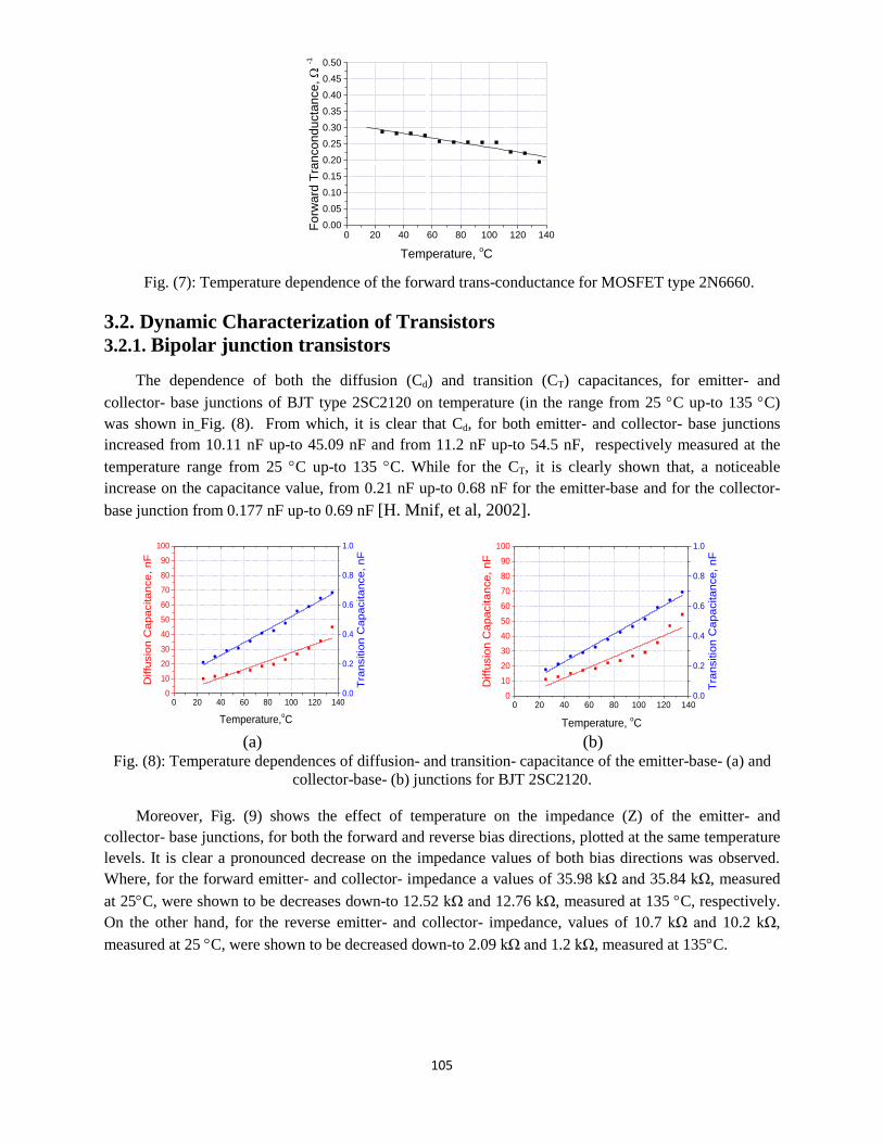
In addition, the forward trans-conductance (gfs) was calculated using Eq.(5), and plotted as
function of temperature [B.L. Theraja, 2008] as shown in Fig. (7). It is clear that gfs was
decreased from 0.292 Ω-1
down-to 0.215 Ω-1,
whenever the devices were exposed to temperature
within the investigated range [A.A. Osman and M. A. Osman, 1998].
gfs
VI
GS
D
= …………………………… (5)
Where,
∆ID: Change in drain current and
∆VGS: Change in gate-source voltage.
0 1 2 3 4 50.0
0.2
0.4
0.6
0.8
1.0T= 25 75 95 115 135
oC
Dra
in C
urr
en
t, A
Gate-Source Voltage, V
20 40 60 80 100 120 1401.50
1.52
1.54
1.56
1.58
1.60
Thre
shold
Voltage, V
Temperature, oC
0 20 40 60 80 100 120 1400
10
20
30
40
50
ON
-Resis
tance,
Temperature, oC
0 20 40 60 80 100 120 1400.12
0.14
0.16
0.18
0.20
0.22
0.24
Dra
in C
urr
en
t, A
Temperature, oC
105
Fig. (7): Temperature dependence of the forward trans-conductance for MOSFET type 2N6660.
3.2. Dynamic Characterization of Transistors
3.2.1. Bipolar junction transistors
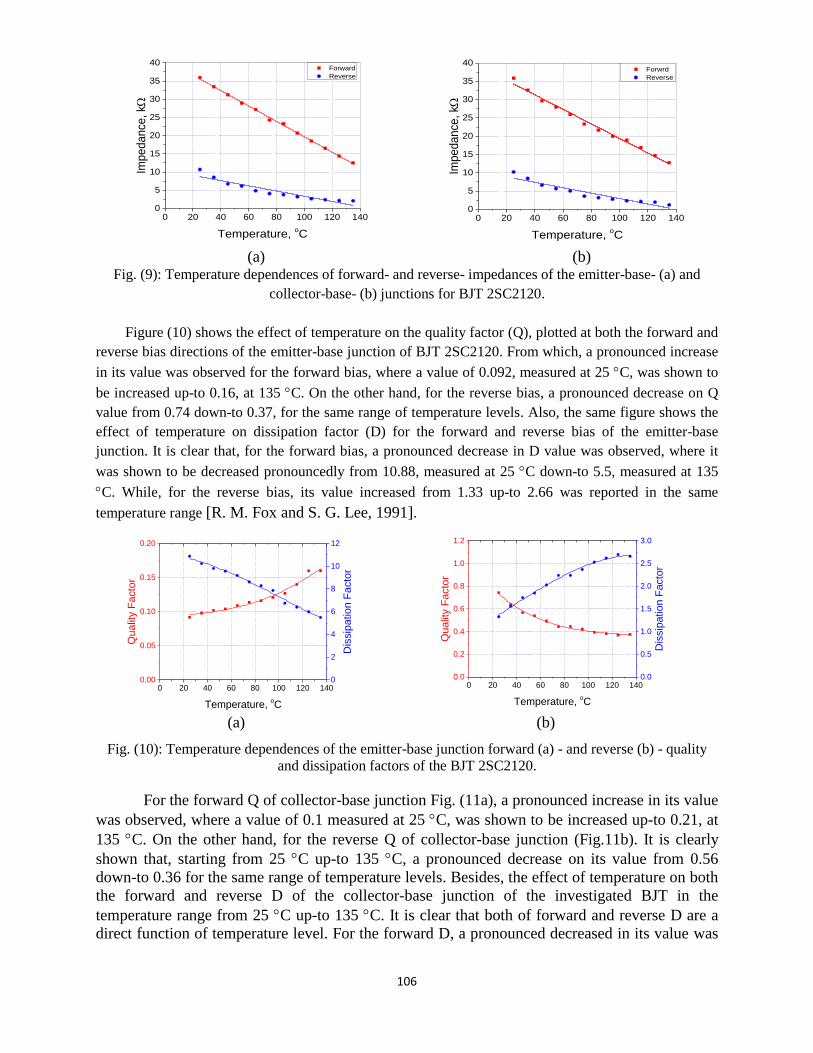
The dependence of both the diffusion (Cd) and transition (CT) capacitances, for emitter- and
collector- base junctions of BJT type 2SC2120 on temperature (in the range from 25 C up-to 135 C)
was shown in Fig. (8). From which, it is clear that Cd, for both emitter- and collector- base junctions
increased from 10.11 nF up-to 45.09 nF and from 11.2 nF up-to 54.5 nF, respectively measured at the
temperature range from 25 C up-to 135 C. While for the CT, it is clearly shown that, a noticeable
increase on the capacitance value, from 0.21 nF up-to 0.68 nF for the emitter-base and for the collector-
base junction from 0.177 nF up-to 0.69 nF [H. Mnif, et al, 2002].
(a) (b) Fig. (8): Temperature dependences of diffusion- and transition- capacitance of the emitter-base- (a) and
collector-base- (b) junctions for BJT 2SC2120.
Moreover, Fig. (9) shows the effect of temperature on the impedance (Z) of the emitter- and
collector- base junctions, for both the forward and reverse bias directions, plotted at the same temperature
levels. It is clear a pronounced decrease on the impedance values of both bias directions was observed.
Where, for the forward emitter- and collector- impedance a values of 35.98 kΩ and 35.84 kΩ, measured
at 25C, were shown to be decreases down-to 12.52 kΩ and 12.76 kΩ, measured at 135 C, respectively.
On the other hand, for the reverse emitter- and collector- impedance, values of 10.7 kΩ and 10.2 kΩ,
measured at 25 C, were shown to be decreased down-to 2.09 kΩ and 1.2 kΩ, measured at 135C.
0 20 40 60 80 100 120 1400
10
20
30
40
50
60
70
80
90
100
Temperature,oC
Diffu
sio
n C
ap
acita
nce
, n
F
0.0
0.2
0.4
0.6
0.8
1.0
Tra
nsitio
n C
ap
acita
nce
, n
F
0 20 40 60 80 100 120 1400
10
20
30
40
50
60
70
80
90
100
Temperature, oC
Diffu
sio
n C
apacitance, nF
0.0
0.2
0.4
0.6
0.8
1.0
Tra
nsitio
n C
apacitance, nF
0 20 40 60 80 100 120 1400.00
0.05
0.10
0.15
0.20
0.25
0.30
0.35
0.40
0.45
0.50
Forw
ard
Tra
nconducta
nce,
-1
Temperature, oC
106
(a) (b) Fig. (9): Temperature dependences of forward- and reverse- impedances of the emitter-base- (a) and
collector-base- (b) junctions for BJT 2SC2120.
Figure (10) shows the effect of temperature on the quality factor (Q), plotted at both the forward and
reverse bias directions of the emitter-base junction of BJT 2SC2120. From which, a pronounced increase
in its value was observed for the forward bias, where a value of 0.092, measured at 25 C, was shown to
be increased up-to 0.16, at 135 C. On the other hand, for the reverse bias, a pronounced decrease on Q
value from 0.74 down-to 0.37, for the same range of temperature levels. Also, the same figure shows the
effect of temperature on dissipation factor (D) for the forward and reverse bias of the emitter-base
junction. It is clear that, for the forward bias, a pronounced decrease in D value was observed, where it
was shown to be decreased pronouncedly from 10.88, measured at 25 C down-to 5.5, measured at 135
C. While, for the reverse bias, its value increased from 1.33 up-to 2.66 was reported in the same
temperature range [R. M. Fox and S. G. Lee, 1991].
(a) (b)
Fig. (10): Temperature dependences of the emitter-base junction forward (a) - and reverse (b) - quality
and dissipation factors of the BJT 2SC2120.
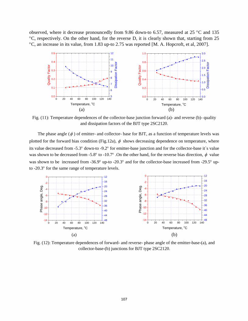
For the forward Q of collector-base junction Fig. (11a), a pronounced increase in its value
was observed, where a value of 0.1 measured at 25 C, was shown to be increased up-to 0.21, at
135 C. On the other hand, for the reverse Q of collector-base junction (Fig.11b). It is clearly
shown that, starting from 25 C up-to 135 C, a pronounced decrease on its value from 0.56
down-to 0.36 for the same range of temperature levels. Besides, the effect of temperature on both
the forward and reverse D of the collector-base junction of the investigated BJT in the
temperature range from 25 C up-to 135 C. It is clear that both of forward and reverse D are a
direct function of temperature level. For the forward D, a pronounced decreased in its value was
0 20 40 60 80 100 120 1400.00
0.05
0.10
0.15
0.20
Temperature, oC
Qualit
y F
acto
r
0
2
4
6
8
10
12
Dis
sip
ation F
acto
r
0 20 40 60 80 100 120 1400
5
10
15
20
25
30
35
40
Imp
ed
an
ce,
k
Temperature, oC
Forward
Reverse
0 20 40 60 80 100 120 1400
5
10
15
20
25
30
35
40
Impedance
, k
Temperature, oC
Forwrd
Reverse
0 20 40 60 80 100 120 1400.0
0.2
0.4
0.6
0.8
1.0
1.2
Temperature, oC
Qu
alit
y F
acto
r
0.0
0.5
1.0
1.5
2.0
2.5
3.0
Dis
sip
atio
n F
acto
r
107
observed, where it decrease pronouncedly from 9.86 down-to 6.57, measured at 25 C and 135
C, respectively. On the other hand, for the reverse D, it is clearly shown that, starting from 25
C, an increase in its value, from 1.83 up-to 2.75 was reported [M. A. Hopcroft, et al, 2007].
(a) (b)
Fig. (11): Temperature dependences of the collector-base junction forward (a)- and reverse (b)- quality
and dissipation factors of the BJT type 2SC2120.
The phase angle ( ) of emitter- and collector- base for BJT, as a function of temperature levels was
plotted for the forward bias condition (Fig.12a), shows decreasing dependence on temperature, where
its value decreased from -5.3 down-to -9.2 for emitter-base junction and for the collector-base it`s value
was shown to be decreased from -5.8 to -10.7 .On the other hand, for the reverse bias direction, value
was shown to be increased from -36.9 up-to -20.3 and for the collector-base increased from -29.5 up-
to -20.3 for the same range of temperature levels.
(a) (b)
Fig. (12): Temperature dependences of forward- and reverse- phase angle of the emitter-base-(a), and
collector-base-(b) junctions for BJT type 2SC2120.
0 20 40 60 80 100 120 1400.0
0.1
0.2
0.3
0.4
0.5
Temperature, oC
Qu
alit
y F
acto
r
5
6
7
8
9
10
11
12
Dis
sip
atio
n F
acto
r
0 20 40 60 80 100 120 1400.0
0.2
0.4
0.6
0.8
1.0
Temperature, oC
Qualit
y F
acto
r
0.0
0.5
1.0
1.5
2.0
2.5
3.0
Dis
sip
ation F
acto
r
0 20 40 60 80 100 120 140-14
-12
-10
-8
-6
-4
-2
0
Temperature, oC
Phase a
ngle
, D
eg.
-48
-44
-40
-36
-32
-28
-24
-20
-16
-12
0 20 40 60 80 100 120 140-14
-12
-10
-8
-6
-4
-2
0
Temperature, oC
-48
-44
-40
-36
-32
-28
-24
-20
-16
-12
Ph
ase
an
gle
, D
eg
.

108
3.2.2 Metal Oxide Field Effect Transistor
The temperature dependence of junction capacitance for the investigated MOSFET was
studied and plotted. In this concern, the drain-source, gate-drain and gate-source junction
capacitances of MOSFET type 2N6660 were studied and plotted as function of temperature Fig.
(13a). From which, it is clearly shown that, the drain-source capacitance decreased from 66.91
pF, measured at 25 C, down to 15.48 pF at 135 C. On the other hand, for the reverse
capacitance, its value was shown to be increased from 41.48 pF up-to 47.31 pF with increasing
temperature from 25 C up-to 135 C. Moreover, for gate-source junction capacitance, it is
clearly shown that, the junction capacitance decreased with increasing temperature from 102.22
pF down-to 96.13 pF. In addition, the temperature dependence of junction impedance (Z) for
drain-source, gate-drain and gate-source junctions of MOSFET device are shown in Fig. (13b).
From which, it is obviously shown that for the drain-source junction Z values was shown to be
decreased from 0.63 kΩ, measured at 25 C, down-to 0.27 kΩ at 135 C. On the other hand, for
the gate-drain junction, its value was shown to be increased from 4.63 kΩ up-to 5.79 kΩ with
increasing temperature from 25 C up-to 135 C, respectively. Moreover, for the gate-source
junction impedance, it is showed that, its value increased from 3.71 kΩ up-to 4.61 kΩ, with
increasing the temperature within the investigated range.
(a) (b)
Fig. (13): Temperature dependences on the drain-source-, gate-drain- and gate-source- junctions-
capacitance (a) and junctions impedance (b) for MOSFET 2N6660.
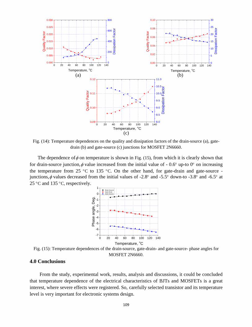
The dependence of Q on temperature for the different junctions is shown in Fig. (14). From
which, it is clearly shown that for drain-source junction, Q value decreased from an initial value
of 0.011 down-to 0.004 on increasing temperature up-to 135 C. On the other hand, for gate-drain
junction and gate-source junction, respectively Q values increased from 0.047 and 0.096,
measured at 25 oC up-to 0.068 and 0.096, at 135
oC. At the same time, it is clearly shown that
for drain-source junction, D was shown to be increased from an initial value of 93.9 up-to 450
for the same temperature levels. On the other hand, for gate-drain- and gate-source - junctions, D
values decreased from the initial value of 20.6 and 10.37, at 25 C down-to 14.47 and 8.71 at
135C [V. V. Orlov, V. A. Felitsyn, G. I. Zebrev, 2016].
0 20 40 60 80 100 120 1400
20
40
60
80
100
120
140
160
Drain-Source
Gate-Source
Gate-Drain
Drain-Source
Gate-Source
Gate-Drain
Temperature, oC
Ca
pa
cita
nce
, p
F
10
20
30
40
50
0 20 40 60 80 100 120 1400
1
2
3
4
5
6
Impedance, k
Temperature, oC
Drain-Source
Gate-Drain
Gate-Source
109
(a) (b)
(c)
Fig. (14): Temperature dependences on the quality and dissipation factors of the drain-source (a), gate-
drain (b) and gate-source (c) junctions for MOSFET 2N6660.
The dependence of on temperature is shown in Fig. (15), from which it is clearly shown that
for drain-source junction, value increased from the initial value of - 0.6 up-to 0 on increasing
the temperature from 25 C to 135 C. On the other hand, for gate-drain and gate-source -
junctions, values decreased from the initial values of -2.8 and -5.5 down-to -3.8 and -6.5 at
25 C and 135 C, respectively.
Fig. (15): Temperature dependences of the drain-source, gate-drain- and gate-source- phase angles for
MOSFET 2N6660.
4.0 Conclusions
From the study, experimental work, results, analysis and discussions, it could be concluded
that temperature dependence of the electrical characteristics of BJTs and MOSFETs is a great
interest, where severe effects were registered. So, carefully selected transistor and its temperature
level is very important for electronic systems design.
0 20 40 60 80 100 120 1400.000
0.005
0.010
0.015
0.020
0.025
0.030
Temperature, oC
Qu
alit
y F
acto
r
0
200
400
600
800
Dis
sip
atio
n F
acto
r
0 20 40 60 80 100 120 1400.00
0.02
0.04
0.06
0.08
0.10
Temperature, oC
Qu
alit
y F
acto
r
0
5
10
15
20
25
30
Dis
sip
atio
n F
acto
r
0 20 40 60 80 100 120 1400.09
0.10
0.11
0.12
Temperature, oC
Qu
alit
y F
act
or
8.0
8.5
9.0
9.5
10.0
10.5
11.0
Dis
sip
atio
n F
act
or
0 20 40 60 80 100 120 140-7
-6
-5
-4
-3
-2
-1
0
1
Phase a
ngle
, D
eg.
Temperature, oC
Drain-Source
Gate-Drain
Gate-Source
110
References:
1. A. S. Sedra , K. C. Smith ,“Microelectronic circuits”, 5th
Ed. , Ch. 5, pp. 377-517,
New York, Oxford university, 2004.
2. A. Osman and M. A. Osman, “Investigation of High Temperature Effects on
MOSFET Transconductance (gm)”, IEEE, the 4th
Intr. High Temp. Electr. Conf.,
INSPEC Accession No. 611441, pp.301-304, 1998.
3. B. Eslamia and S. Ashrafib, “Effect of gamma ray absorbed dose on the FET
transistor parameters”, Results in Physics, Vol. 6, pp. 396-400, 2016.
https://doi.org/10.1016/j.rinp.2016.07.003
4. B.L. Theraja and A.K. Theraja, “A.T.B. of Electrical Technology", Chs. 57 and
63 pp. 2187-2218 and 2188-2218, 2008.
5. E. Schurackm, et al, “Nonlinear effects in transistors caused by thermal power
feedback: simulation and modeling in spice”, Proc. IEEE Intr. Symposium on
Circuits and Systems, Vol.6, pp.879-882, 1992.
6. H. Djelti, et al, “Two dimensional numerical simulation of temperature
dependency of MOSFET out-put characteristics”, IEEE, STIC Lab., 2008.
7. H. Mnif, et al, “A new approach for modeling the thermal behavior of bipolar
transistors”, IEEE, 4th
Intr. Caracas Conf. on Devices, Circuits and Systems, pp.
DO241- DO24 5, INSPEC Accession No. 7374389, 2002.
8. J. Millman and C.C. Halkias, “Integrated Electronics: Analog and Digital Circuits
and Systems”, 3rd
Ed., Ch. 5, pp. 118-158, USA, 1972.
9. M. A. Hopcroft, et al, “Using the temperature dependence of resonator quality
factor as a thermometer”, Appl. Phys. Lett. 91, pp. 013505-1- 013505-3,
American Institute of Physics, DOI: 10.1063/1.2753758, 2007.
10. N. Rinaldi and V. Alessandro, “Theory of electro thermal behavior of bipolar
transistors”, IEEE Trans. on Electronic Devices, Part I : Single-Finger Devices,
Vol. 52, No.9, 2005.
11. R. M. Fox and S. G. Lee, “Predictive modeling of thermal effects in BJTs”, IEEE
Jour, university of Florida, pp. 98-92, 1991.
12. S. Bethi, et al, “A temperature and process insensitive CMOS only reference
current generator”, M.Sc. Thesis, Faculty of The University of Akron, 2014.
111
13. T. D. Haeffner, “Irradiation and temperature characterization for a 32NM RF
silicon-on-insulator CMOS process”, M.Sc. Thesis, Nashville, Tennessee, 2015.
14. “Thermal Stability of MOSFETs”, Application Note, Semiconductor Components
Industries, LLC, No. AND8199/D, 2014. http://onsemi.com
15. V. V. Orlov, V. A. Felitsyn and G. I. Zebrev, “Compact modeling of I-V
characteristics in irradiated MOSFETs: impact of operation temperature and
interface traps”, IEEE, the 16th
Eurpoen Conf. on Radiation and its Effects on
Components and System (RADECS), INSPEC Accession No. 17335345, 2016.
16. Y. Agiwa, et al., “Reliability study of mounting structure for high temperature
power semiconductor device chip using high purity aluminum”, In Proc. Thermal
and Thermo mechanical Phenomena Electronic System, Orlando, FL., U.S.A, pp.
906 – 912, 2008

112
انهخض انعرب
و ترازصتىر تأحر انجبل تتأحر انحرارة عه انخظبئض انكهربت نبطت ترازصتىر حبئ انقطب
الأكضذ انعذ
رهبو أصبيت انضعذ إبراهى(1)
صهب يحذ عبذ انعظى -(1)
طفبء يحذ رشذ انغبو(1)
فؤاد عبذ انعى صعذ صهب -(2 )
-
-انقبهرة- جبيعت ع شش -كهت انببث نلؤداة وانعهىو وانتربت -ى انفزبءقض -يعم أبحبث الإنكتروبث .1
انعربت جهىرت يظر
جهىرت يظر انعربت -انقبهرة -11721 -انعبدي - 535 ص ة. -هئت انىاد انىوت .2
)مىحىبث انخبس وانجهذ ( كهشبت الاسخبحكت حطبقت عه انخصبئص اندساست عمهت انمعشوض حىبول انبحذ
حشاوضسخىس حأرش انمجبل الأكسذ انمعذو ححج و تنىبطخ حشاوضسخىس رىبئ انقطب )مىحىبث انسعت وانجهذ( وانذىبمكت
انعمهت انىخبئجأظهشث حذ مئىت.دسجت 135ºCحخ ºC52 مه دسجت حشاسة انغشفت ، ف انمذي انمشحفعت حأرش انحشاسة
مه كسب انخبس صبدة مهحىظت ف حبس انمجمع وؤد إن 2SC2120أن حأرش انحشاسة عه حشاوضسخىس رىبئ انقطب
0.198A 0.25 حخA 25انغشفت حشاسة ف انمذي مه دسجت عه انخىان 0.50 حخ 0.0.0ومهºC 135حخºC .
وعه انجبوب عىذ وفس انمذي انمشبس إن مه دسجبث انحشاسة. قبست ، م0.42V حخ 0.62V بىمب قم جهذ انعخبت ن مه
حذود وضح، الامش انزي أ حم دساست انعلاقت به انسعت وانجهذ عىذ دسجبث حشاسة مخخهفت ، فقذاخش نهخصبئص انذىبمكت
10.11nFىس حذ صادث مه انببعذ وانقبعذة ف حبنت انخىصم الأمبم نهخشاوضسخ وصهخ بهانمكزف سعتف قمت صبدة
. 45.09nFحخ
حم ملاحظت حذود اضمحلال فقذ 2N6660أمب ببنىسبت إن حأرش انحشاسة عه حشاوضسخىس حأرش انمجبل الأكسذ انمعذو
A, 5 Ω 1.2مه ورنك مه انقم انخىصهت حبس انمصشف و مه كلاا ف قمت -1
A, 1.9 Ω 0.79 حخ -1
مه دسجت ابخذاءاا
جهذ انعخبت. وعه انجبوب اخش نم حؤرش انحشاسة عه قمعه انخىان. بىمب ºC 135حخ ºC 25انغشفت حشاسة
، ومه رنك عه سبم انمزبل ، فقذ وانجهذ عىذ دسجبث حشاسة مخخهفت حم دساست انعلاقت به انسعت ، فقذنهخصبئص انذىبمكت
بضبدة pF 47.31حخ pF 41.48انسعت انعكست عه انىصهت به انبىابت وانمصشف مه بدي ف قمصحذود ملاحظتحم
.ف انمذي انمزكىس انحشاسة
: اصبء انشبرك ببنبحج
رئش قضى انهذصت و - ثأصتبر هذصت الإنكتروبث وانحبصبب) انعى صعذ صهب / فؤاد عبذ .و..دأ -1
(. انىوت هئت انىاد- تالإنكترو
كهت انببث نلآداة وانعهىو –قضى انفزبء –د./ طفبء يحذ رشذ انغبو ) أصتبر يضبعذ الإنكتروبث -2
جبيعت ع شش (. –وانتربت
كهت انببث نلآداة وانعهىو –قضى انفزبء -د./ صهب يحذ عبذ انعظى أحذ ) يذرس الإنكتروبث -3
جبيعت ع شش (. –وانتربت
–كهت انببث نلآداة وانعهىو وانتربت –قضى انفزبء -أصبيت انضعذ إبراهى ) ببحخت يبجضتر رهبو -4
جبيعت ع شش (.