Embed Size (px)
Citation preview
http://www.alliedacademies.org/advanced-materials-science-research/
Adv Mater Sci Res 2016 Volume 1 Issue 114
Research Article
IntroductionVaristors or variable resistors are sintered polycrystalline ceramics have been used as surge protective device for decades. The main reason for using varistor is non-linear current-voltage (V-I) characteristics and excellent energy absorption capability. ZnO varistors were first utilized for the protection of semiconductor devices against transient surges in Electronic equipment. Later ZnO varistors were extensively used as surge absorbers in industrial equipment, and the fields of applications have risen regularly. At lower voltage, varistors act as resistors. However, they become conductors at higher voltages and described by the empirical equation [1-4], I=KVα where K is geometry constant of the sample, α is the non-linearity coefficient, I the current across the sample, and V voltage applied to the varistors. The non-linear current-Voltage characteristics depend on the microstructure and composition, such as grain size, morphology, distribution of secondary phases. By controlling these parameters, the non-linearity coefficient and breakdown field of ZnO varistors may be increased significantly [1-8].
The electrical properties of ZnO based ceramics are very sensitive to the grain boundary because the varistors non-linear coefficient and breakdown voltage depends on the grain boundary. Therefore, numerous studies are suggesting the grain boundary phenomena Of ZnO-Bi2O3 [9-11] and ZnO-V2O5 based ceramic systems [11,12].
It is vital to the comprehension of the mechanism controlling the grain boundary process of ZnO-based varistor ceramics in a more efficient way according to the manufacturer to tailor the grain boundary behavior of ZnO-based varistor ceramics in a more efficient way according to the specific demands of applications. The grain boundary behavior can be profoundly
affected by the dopants. Chen et al. [13] found the values of breakdown field E1mA/Cm2 and non-linear coefficient strongly depend on the resistivity of the grain boundary. Wu et al. [9] studied the influence of MnO2, PbO and a mixture of MnO2, PbO and B2O3 on electrical and dielectric properties of ZnO-V2O5 ceramics by alternating current (AC) impedance and variable temperature dielectric spectroscopy and found that the Schottky barrier present at grain boundary is much more important for varistor performance. In our previous study [13], the electrical conductivity of Mn doped and Co doped ZnO-Bi2O3 varistors were investigated using complex plane modulus analysis and found that the ratio of grain boundary to grain resistance of Mn doped samples is higher than that of Co doped samples. Hng [14] found that electrical characteristics of ZnO-V2O5 doped with MgO critically depend on the grain boundary resistance using impedance spectroscopy.
Therefore, it is necessary that MgO doped ZnO-V2O5-MnO ceramic system will be studied in terms of sintering temperature and grain boundary behavior to tailor multi-layered chip varistors [13].
In the present investigations studies, have been made on the effect of sintering temperatures (850°C, 900°C, and 950°C) on the microstructure and electrical properties of MnO and MgO doped ZnO-0.5 mol% V2O5 varistor system.
Experimental Procedure High purity reagent grade Sigma-Aldrich ZnO (>99.00%), V2O5 (99.60%), MgO (99.5%), MnCO3 (99.0%) were used as raw materials. To investigate the effect of sintering temperature on various structural and electrical characteristics compositions (97.4 mol% ZnO + 0.5 mol% V2O5 + 2 mol% MnO + 0.1
The effect of sintering temperature on the microstructure and the electrical response of liquid phase sintered ZnO-V2O5 varistor ceramics were analyzed using A.C impedance spectroscopy on samples prepared via conventional solid route. The impedance spectra were analyzed with the help of the model equivalent circuit at high frequencies and another at low frequencies, involving both resistor and constant phase element (CPE). The results indicate a significant contribution of grain boundary resistance to the non-ohmic characteristic of the studied materials. The products were characterized regarding phase with X-ray diffraction, microstructures with SEM. Electrical characteristics were studied with impedance analysis and current-voltage characterization. In the present investigations studies, have been made on the effect of sintering temperatures (850°C, 900°C, and 950°C) on the microstructure and electrical properties of MnO and MgO doped ZnO-0.5 mol% V2O5 varistor system. The phase composition of samples consists mainly ZnO grains, while Zn2VO4 is the secondary phases. Better varistor performance has been achieved for the samples sintered at 950°C with non-linear coefficient α=16, breakdown voltage 2513.3 V/mm and leakage current is JL=7.7 × 10⁻⁵ A/cm2. SEM analysis of morphology shows that the grain growth increases with increase in sintering temperature.
Abstract
Effect of sintering temperature on electrical characteristics of ZnO-0.5 mol% V2O5-2 mol% MnO varistors.
Noolu SM Viswanath*, Shreevats Pandey, Devendra KumarDepartment of Ceramic Engineering, Indian Institute of Technology Banaras Hindu University, Varanasi, India
Accepted on November 24, 2016
Keywords: Microstructure; ZnO; V2O5; MnO; MgO; Sintering temperature; Varistors
Citation: Viswanath NSM, Pandey S, Kumar D. Effect of sintering temperature on electrical characteristics of ZnO-0.5 mol% V2O5-2 mol% MnO varistors. Adv Mater Sci Res. 2016;1(1):14-19.
15Adv Mater Sci Res 2016 Volume 1 Issue 1
mol% MgO) was prepared. All the samples were mixed by conventional ball milling with zirconia balls and acetone in a polypropylene bottle for 24 hours. The mixtures were filtered, dried and calcined at 700°C for 3 hrs. The agglomerate was pulverized using an agate mortar-pestle. The powder mixture was pressed in disc shape specimens in a hydraulic press at 90 kN load using polyvinyl butyral (PVB) as a binder. The pellets were sintered at 850°C, 900°C and 950°C for 2 hrs with heating and cooling rate of 5°C/min using a double alumina crucible method. In this method, the samples are covered with raw powder and an inverted crucible during sintering. The sintered specimens were polished by emery paper on the both sides and annealed at 700°C for 5 hrs to stabilize the electrical properties. Before performing electrical measurements, the conductive silver paste was coated on both surfaces of the pellets and the electrodes were formed by heating it at 600°C for 10 min.
Structural characterizationPowder X-ray diffraction is used to determine the phase composition of sintered samples. Powder X-ray diffraction patterns were recorded using Cu Kα radiation with Ni filter on a vertical powder diffractometer. Data were collected in the 2θ range from 200 to 800 in an oxygen atmosphere. The lattice parameters for hexagonal structure were calculated using cell software [12].
For microstructural observations, the surfaces of sintered samples were polished by emery papers of grade 1/0, 2/0, 3/0 and 4/0. These surfaces were again polished to mirror-like by velvet cloth with a diamond paste of grade ¼-OS-475 (HIFIN). The polished surfaces were thermally etched at 750°C for 10 min. The microstructures of polished samples were examined by scanning electron microscope (INSPECT 50 FEI). The average grain size G were measured directly from the micrographs of etched samples by linear intercept method, as described by [15]. G=1:56 (L/MN) where L is the length of the micrograph, M is the magnification of micrograph, and N is the no. of grain boundaries.
Electrical measurementThe electrical characteristics (E-J) were measured by using V-I source/measuring unit (Keithley 2410). The breakdown field was measured at E1mA/cm2 and the leakage current (JL) was measured at 0.75 E10 mA/cm2. The non-linearity coefficient defined by empirical formula J=KEα. Where J is the current density, E is the applied electric field; α is the non-linearity coefficient and K is constant. Non-linearity coefficient determined by the formula is α=1/ (logE2 to logE1), and it is identified in the range of 1.0 mA/cm2 to 10 mA/cm2. Where E1 and E2 are the electric field at 1 mA/cm2 and 10 mA/cm2, respectively [1-5].
Impedance analysisWhen polycrystalline ceramics subjected to alternative electric field shows contributions from grain and grain boundary. Complex plane impedance analysis is an effective tool to separate grain and grain boundary contributions. An alpha high-performance frequency analyzer Novo control Technologies was employed to measure the impedance spectroscopy in the frequency range of 10 mHz to 1 MHz with 1V applied AC signal at a temperature 323 K to 723 K. The obtained experimental
results were fitted using Z-view software for modeling and analysis of impedance spectroscopy measurements involving resistance and CPE (constant phase element).
Results and DiscussionXRD analysisFigure 1 shows that XRD patterns of ZnO doped with 0.1 mol% of MgO doping. This data obtained by preparing the samples at sintering temperatures 850°C, 900°C and 950°C for 2 hrs. The patterns confirmed the presence of dominant ZnO phase (JCPDS 36-1451) and Zn2VO4 (JCPDS 76-1632) as minor secondary phases. The lattice parameter and % of Zn2VO4 are given in Table 1. The highest lattice parameter of ZnO varistors are due to the Mn+2 (0.080 nm) ions which have high ionic radii compared to Zn+2 (0.079 nm) segregated at the grain boundaries as a secondary phases. When the sintering temperature increases from 850°C to 900°C the amount of secondary phase increases from 1.52% to 1.71% and at 950°C it is decreased to 1.44%. As impurity level increases the electron hole pairs at the grain boundaries decreases which leads to decrease in nonlinear characteristics [16].
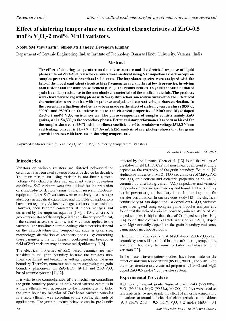
Microstructural observationsFigure 2 shows the SEM micrographs of ZnO-V2O5-MnO system sintered at 850°C, 900°C, and 950°C for 0.1% doping of MgO. SEM analysis reveals the differences in average grain size and shapes of the ZnO-V2O5-MnO system was studied. The largest average grain size belongs to ZnO-V2O5-MnO system sintered at 950°C was 4.10 µm. Bulky and exaggerated grains were noticed at this sintering temperature. The sample sintered at 850°C shows that grain structure is non-uniformly distributed, while increasing the sintering temperature from 850°C to 950°C the non-uniformity decreased and average grain size increases from 2.41 µm to 4.10 µm.
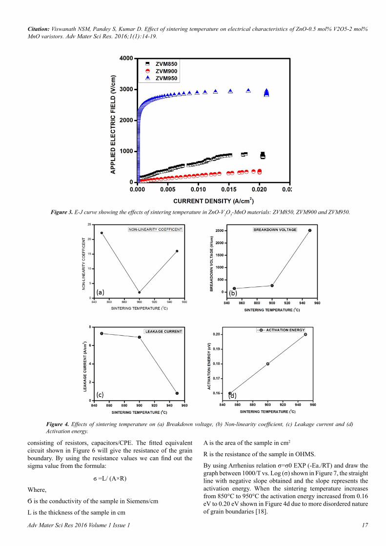
Current-voltage characteristicsFigure 3 shows the J-E characteristics of samples for various sintering temperatures. The curves are divided into two regions: one is non-ohmic region with extremely low impedance after breakdown field and other is ohmic region with extremely high impedance before breakdown field. The sharper the knee of the curve between two regions the better the varistor properties. It can be seen from the curves the sintering temperature has a significant effect on varistor properties. The detailed J-E characteristics parameters are summarized in Table 2.
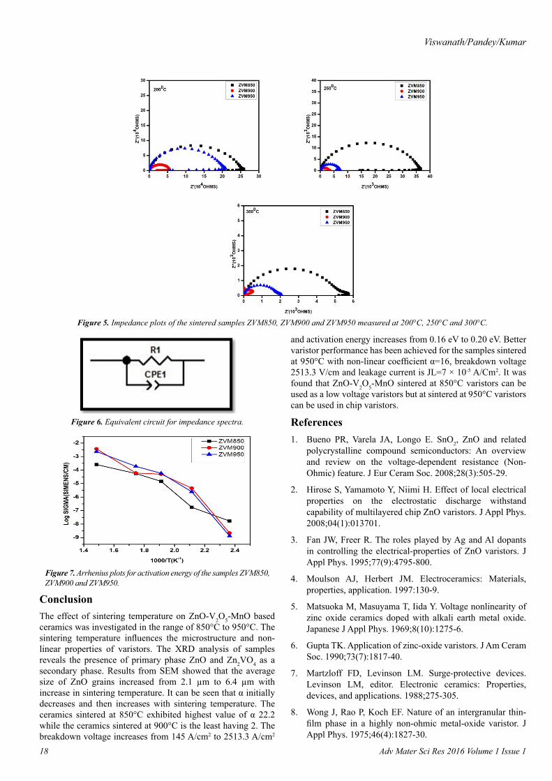
As the increase in sintering from 850°C to 900°C the breakdown field increases from 145 V/cm to 265 V/cm but abrupt change of breakdown field takes place when sintering temperature increases upto 950°C and α is also increased from 2 to 16. As a result, it can be seen that the sintering temperature has a significant effect on the non-linear properties.
The behaviour of α is accordance with sintering temperatures, temperature can related to the variation of Schottky barrier according to the variation of electronic states at the grain boundaries. Therefore, the decrease of α in accordance with sintering temperature is attributed to the decrease in potential barrier height at the grain boundaries.
The variation of α against sintering temperature is shown in
Viswanath/Pandey/Kumar
16 Adv Mater Sci Res 2016 Volume 1 Issue 1
Figure 4a. As the sintering temperature increases from 850°C to 900°C the α value decreases due to decrease of recombination current between electrons and holes in the vicinity of grain boundaries. α is enhanced when the sintering temperature increased to 950°C which suggests that segregation of Zn2VO4 at the grain boundary has promoted the development of needed potential barrier at interface. On the other hand, when the sintering temperature increases from 850°C to 950°C leakage current decreased from 7.3 µA/cm2 to 0.9 µA/cm2 shown in Figure 4c. This is due to the reduction of barrier height [17].
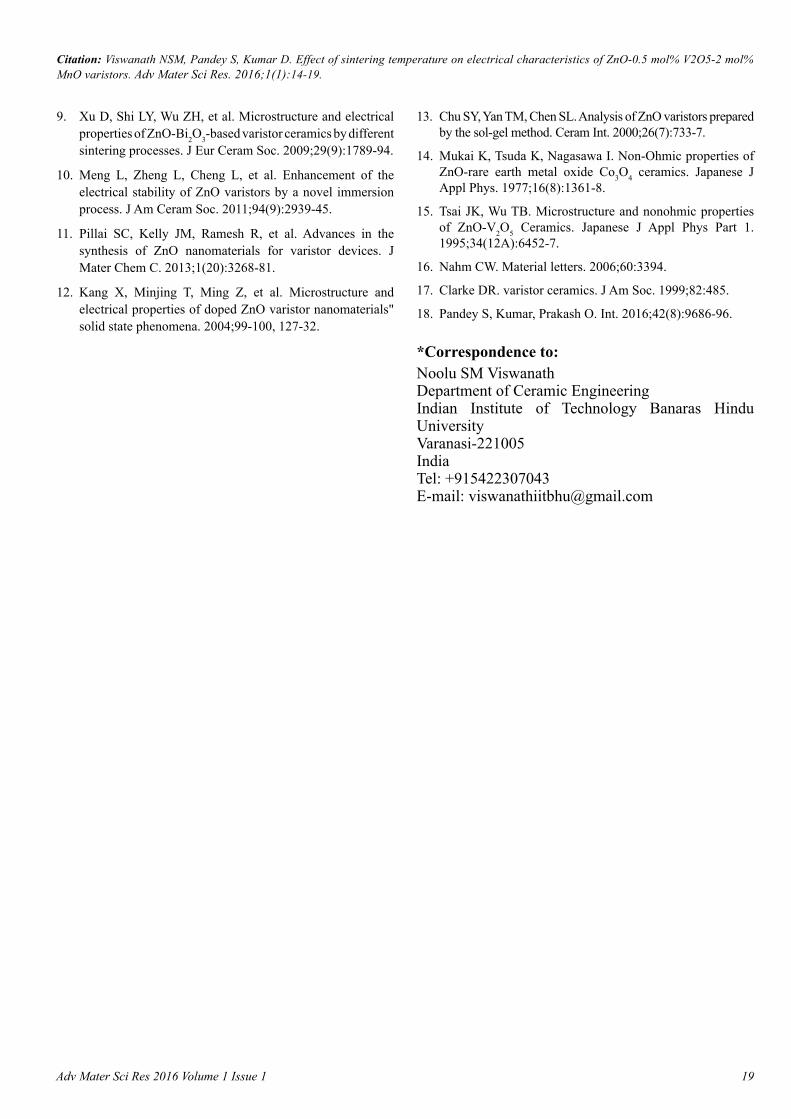
Figure 5 shows the raw impedance spectra as a function of temperature in air. In all the impedance plots only single arc is
observed under all experimental conditions. Each arc is a semi-circle with its origin on the real axis. The resistance, equal to the diameter of the each arc, decreases systematically with increasing in temperature. There are several possible explanations for the temperature dependence of the electrical properties as surface adsorption of oxygen could alter the surface charge state and thereby the carrier population in the near-surface depletion layers of the each particle. We favor the model based upon resistive grain boundaries and highly conductive grain cores. To find out the resistances these impedance plots were fitted in Z-view software, for the modeling and analysis of impedance spectroscopy measurements regarding equivalent circuits
Figure 1. XRD traces of (a) ZVM850, (b) ZVM900 and (c) ZVM950.
Figure 2: SEM micrographs of (a) ZVM850, (b) ZVM900 and (c) ZVM950.
Samples a (A°) b (A°) c (A°) Unit cell volume (A°3)
Amount of impurity (%)
ZVM850 11.469 11.469 3.071 404.002 1.52ZVM900 11.831 11.831 3.066 429.273 1.71ZVM950 11.439 11.439 3.074 402.315 1.44
Table 1. Lattice parameter and impurity level of ZnO-V2O5-MnO-MgO varistor ceramics.
Samples (E1mA/Cm2)
JL(10-4 A/Cm2) α Activation
energy (eV)Average rain
size (µm)ZVM850 145 7.3 22.2 0.16 2.41ZVM900 265 6.9 2 0.18 3.69ZVM950 2513.3 0.8 16 0.20 4.17
Table 2. Summary of sample, average grain size and electrical results for the different ZnO-V2O5-MnO-MgO varistor ceramics.
Citation: Viswanath NSM, Pandey S, Kumar D. Effect of sintering temperature on electrical characteristics of ZnO-0.5 mol% V2O5-2 mol% MnO varistors. Adv Mater Sci Res. 2016;1(1):14-19.
17Adv Mater Sci Res 2016 Volume 1 Issue 1
consisting of resistors, capacitors/CPE. The fitted equivalent circuit shown in Figure 6 will give the resistance of the grain boundary. By using the resistance values we can find out the sigma value from the formula:
ϭ =L/ (A×R)
Where,
Ϭ is the conductivity of the sample in Siemens/cm
L is the thickness of the sample in cm
A is the area of the sample in cm2
R is the resistance of the sample in OHMS.
By using Arrhenius relation σ=σ0 EXP (-Ea./RT) and draw the graph between 1000/T vs. Log (σ) shown in Figure 7, the straight line with negative slope obtained and the slope represents the activation energy. When the sintering temperature increases from 850°C to 950°C the activation energy increased from 0.16 eV to 0.20 eV shown in Figure 4d due to more disordered nature of grain boundaries [18].
Figure 3. E-J curve showing the effects of sintering temperature in ZnO-V2O5-MnO materials: ZVM850, ZVM900 and ZVM950.
Figure 4. Effects of sintering temperature on (a) Breakdown voltage, (b) Non-linearity coefficient, (c) Leakage current and (d) Activation energy.
Viswanath/Pandey/Kumar
18 Adv Mater Sci Res 2016 Volume 1 Issue 1
ConclusionThe effect of sintering temperature on ZnO-V2O5-MnO based ceramics was investigated in the range of 850°C to 950°C. The sintering temperature influences the microstructure and non-linear properties of varistors. The XRD analysis of samples reveals the presence of primary phase ZnO and Zn2VO4 as a secondary phase. Results from SEM showed that the average size of ZnO grains increased from 2.1 µm to 6.4 µm with increase in sintering temperature. It can be seen that α initially decreases and then increases with sintering temperature. The ceramics sintered at 850°C exhibited highest value of α 22.2 while the ceramics sintered at 900°C is the least having 2. The breakdown voltage increases from 145 A/cm2 to 2513.3 A/cm2
and activation energy increases from 0.16 eV to 0.20 eV. Better varistor performance has been achieved for the samples sintered at 950°C with non-linear coefficient α=16, breakdown voltage 2513.3 V/cm and leakage current is JL=7 × 10⁻⁵ A/Cm2. It was found that ZnO-V2O5-MnO sintered at 850°C varistors can be used as a low voltage varistors but at sintered at 950°C varistors can be used in chip varistors.
References1. Bueno PR, Varela JA, Longo E. SnO2, ZnO and related
polycrystalline compound semiconductors: An overview and review on the voltage-dependent resistance (Non-Ohmic) feature. J Eur Ceram Soc. 2008;28(3):505-29.
2. Hirose S, Yamamoto Y, Niimi H. Effect of local electrical properties on the electrostatic discharge withstand capability of multilayered chip ZnO varistors. J Appl Phys. 2008;04(1):013701.
3. Fan JW, Freer R. The roles played by Ag and Al dopants in controlling the electrical-properties of ZnO varistors. J Appl Phys. 1995;77(9):4795-800.
4. Moulson AJ, Herbert JM. Electroceramics: Materials, properties, application. 1997:130-9.
5. Matsuoka M, Masuyama T, Iida Y. Voltage nonlinearity of zinc oxide ceramics doped with alkali earth metal oxide. Japanese J Appl Phys. 1969;8(10):1275-6.
6. Gupta TK. Application of zinc-oxide varistors. J Am Ceram Soc. 1990;73(7):1817-40.
7. Martzloff FD, Levinson LM. Surge-protective devices. Levinson LM, editor. Electronic ceramics: Properties, devices, and applications. 1988;275-305.
8. Wong J, Rao P, Koch EF. Nature of an intergranular thin-film phase in a highly non-ohmic metal-oxide varistor. J Appl Phys. 1975;46(4):1827-30.
Figure 5. Impedance plots of the sintered samples ZVM850, ZVM900 and ZVM950 measured at 200°C, 250°C and 300°C.
Figure 6. Equivalent circuit for impedance spectra.
Figure 7. Arrhenius plots for activation energy of the samples ZVM850, ZVM900 and ZVM950.
Citation: Viswanath NSM, Pandey S, Kumar D. Effect of sintering temperature on electrical characteristics of ZnO-0.5 mol% V2O5-2 mol% MnO varistors. Adv Mater Sci Res. 2016;1(1):14-19.
19Adv Mater Sci Res 2016 Volume 1 Issue 1
9. Xu D, Shi LY, Wu ZH, et al. Microstructure and electrical properties of ZnO-Bi2O3-based varistor ceramics by different sintering processes. J Eur Ceram Soc. 2009;29(9):1789-94.
10. Meng L, Zheng L, Cheng L, et al. Enhancement of the electrical stability of ZnO varistors by a novel immersion process. J Am Ceram Soc. 2011;94(9):2939-45.
11. Pillai SC, Kelly JM, Ramesh R, et al. Advances in the synthesis of ZnO nanomaterials for varistor devices. J Mater Chem C. 2013;1(20):3268-81.
12. Kang X, Minjing T, Ming Z, et al. Microstructure and electrical properties of doped ZnO varistor nanomaterials" solid state phenomena. 2004;99-100, 127-32.
13. Chu SY, Yan TM, Chen SL. Analysis of ZnO varistors prepared by the sol-gel method. Ceram Int. 2000;26(7):733-7.
14. Mukai K, Tsuda K, Nagasawa I. Non-Ohmic properties of ZnO-rare earth metal oxide Co3O4 ceramics. Japanese J Appl Phys. 1977;16(8):1361-8.
15. Tsai JK, Wu TB. Microstructure and nonohmic properties of ZnO-V2O5 Ceramics. Japanese J Appl Phys Part 1. 1995;34(12A):6452-7.
16. Nahm CW. Material letters. 2006;60:3394.
17. Clarke DR. varistor ceramics. J Am Soc. 1999;82:485.
18. Pandey S, Kumar, Prakash O. Int. 2016;42(8):9686-96.
*Correspondence to:Noolu SM ViswanathDepartment of Ceramic EngineeringIndian Institute of Technology Banaras Hindu UniversityVaranasi-221005IndiaTel: +915422307043E-mail: [email protected]