Embed Size (px)
Citation preview
Synchronous Digital Design Methodology and Guidelines
Digital System Design
Synchronous Design
• All flip-flops clocked by one common clock
• Reset only used for initialization
• Races and hazards are no problem
Why synchronous design?
• Hazard
• Race– Problems due to timing that cannot be observed
from functional analysis
Timing Hazard• Static hazard: possibility of a brief signal
value change when the signal was expected to be stable, due to timing (glitch)
• Dynamic hazard: possibility of multiple output transitions caused by a single input transition due to multiple signal paths with different delays
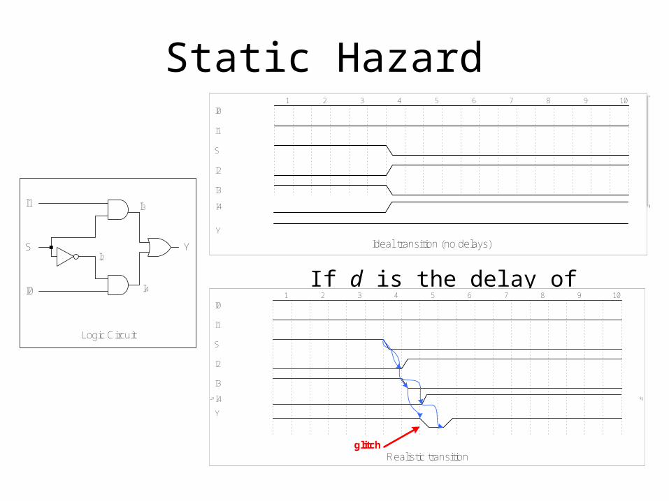
Static Hazard
S
I0
I1
Y
Logic Circuit
I2
I3
I4
1 2 3 4 5 6 7 8 9 10
I0
I1
S
I2
I3
I4
Y
Ideal transition (no delays)
If d is the delay of each gate 1 2 3 4 5 6 7 8 9 10
I0
I1
S
I2
I3
I4
Y
glitchRealistic transition
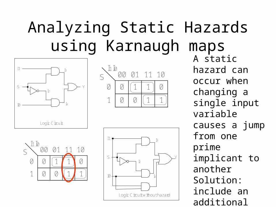
Analyzing Static Hazards using Karnaugh maps
I1I000
0
01
1
11 10S0 1 1 0
0 0 1 1
S
I0
I1
Y
Logic Circuit
I2
I3
I4
I1I000
0
01
1
11 10S0 1 1 0
0 0 1 1
A static hazard can occur when changing a single input variable causes a jump from one prime implicant to anotherSolution: include an additional prime implicantS
I0
I1
Y
Logic Circuit without hazard
I2
I3
I4
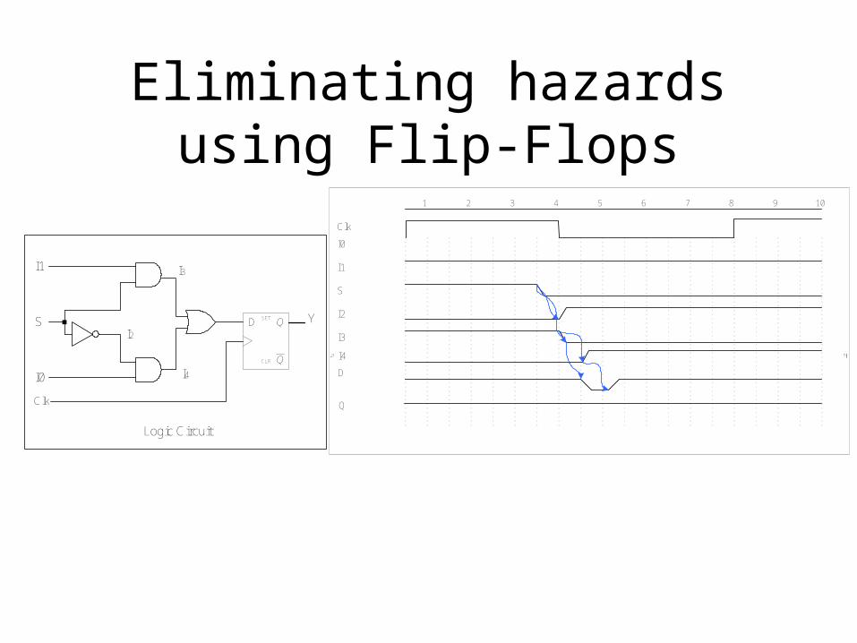
Eliminating hazards using Flip-Flops
S
I0
I1
Y
Logic Circuit
I2
I3
I4Q
QSET
CLR
D
Clk
1 2 3 4 5 6 7 8 9 10
I0
I1
S
I2
I3
I4
D
Clk
Q
Synchronous Design
• Three things must be ensured by the designer:– Minimize and determine clock skew– Account for flip-flop setup and hold times– Reliably synchronize asynchronous inputs
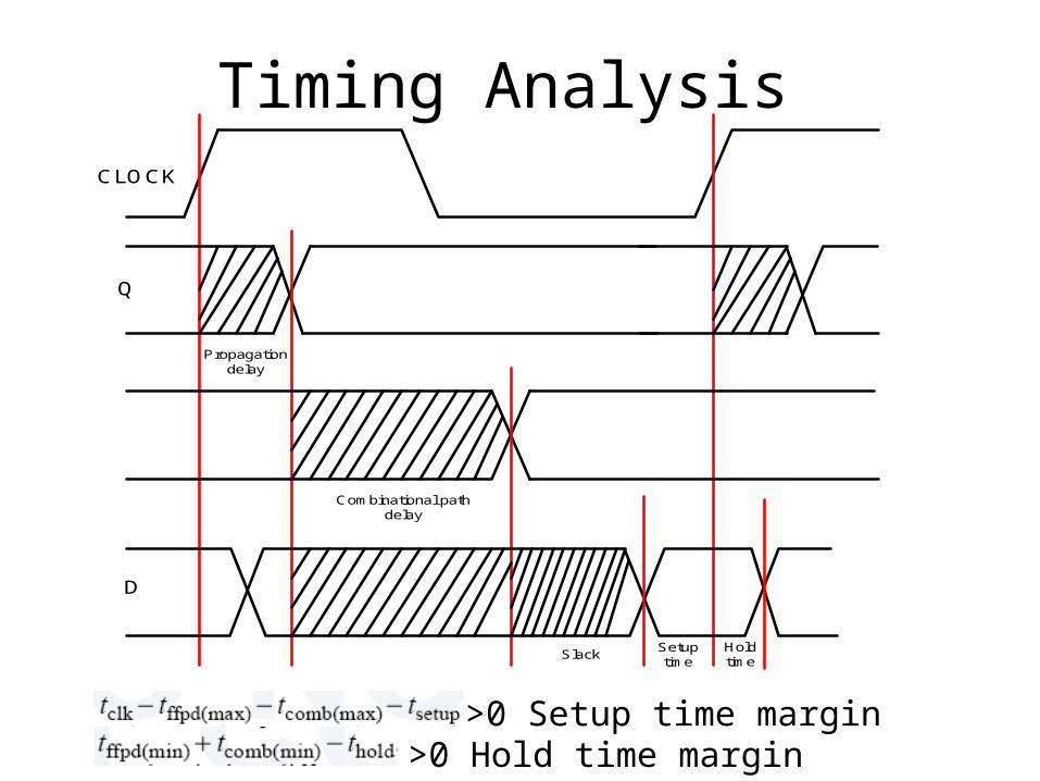
Timing AnalysisCLOCK
Q
Propagation delay
Combinational path delay
Setup time
Hold time
Slack
D
>0 Setup time margin>0 Hold time margin
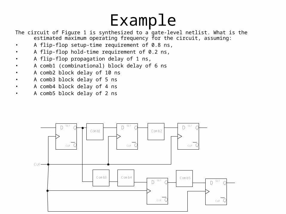
ExampleThe circuit of Figure 1 is synthesized to a gate-level netlist. What is the estimated maximum operating frequency
for the circuit, assuming:• A flip-flop setup-time requirement of 0.8 ns,• A flip-flop hold-time requirement of 0.2 ns,• A flip-flop propagation delay of 1 ns,• A comb1 (combinational) block delay of 6 ns• A comb2 block delay of 10 ns• A comb3 block delay of 5 ns• A comb4 block delay of 4 ns• A comb5 block delay of 2 ns
Q
QSET
CLR
D
Q
QSET
CLR
DComb1
CLK
Comb3
Q
QSET
CLR
D
Q
QSET
CLR
DComb2
Comb4
Q
QSET
CLR
DComb5
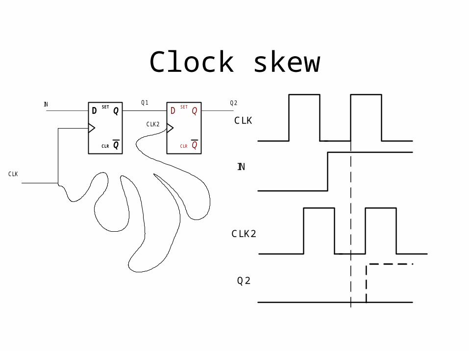
Clock skew
Q
QSET
CLR
D
Q
QSET
CLR
D
CLK
IN Q1 Q2
CLK2 CLK
IN
Q2
CLK2

Example• Determine the maximum frequency of the
following circuit with and without skew
Q
QSET
CLR
D
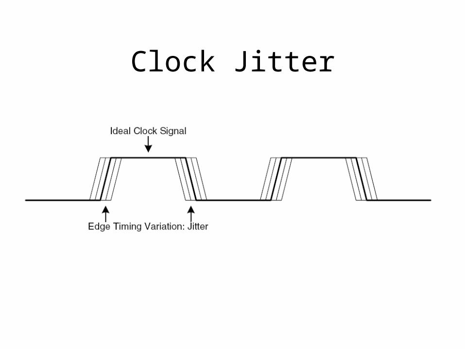
Clock Jitter
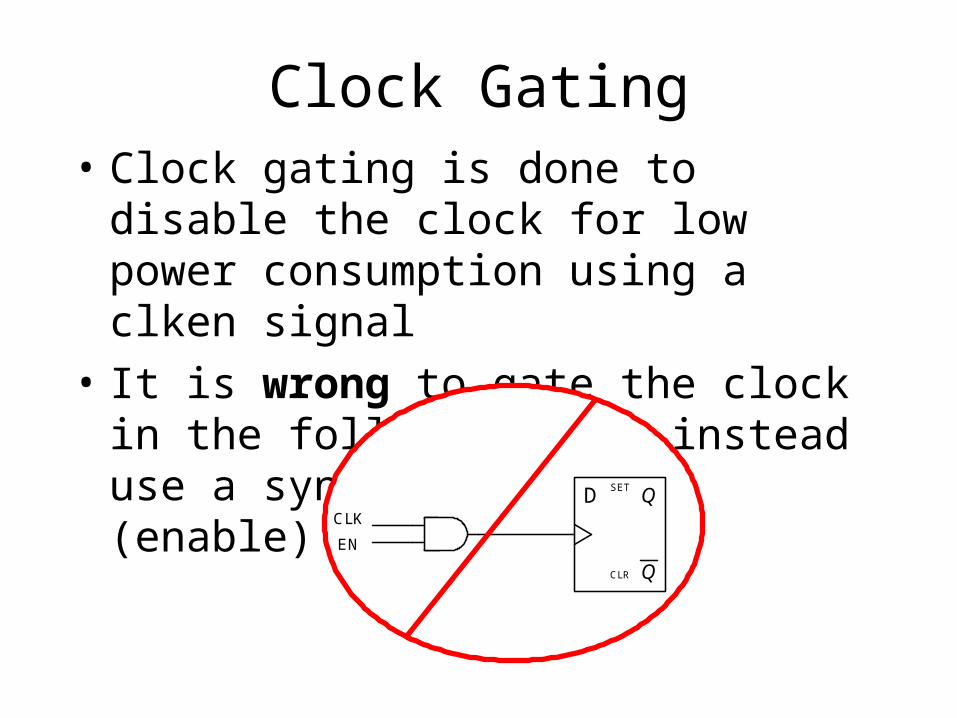
Clock Gating• Clock gating is done to disable the clock for
low power consumption using a clken signal
• It is wrong to gate the clock in the following way, instead use a synchronous load (enable) signal
Q
QSET
CLR
DCLK
EN
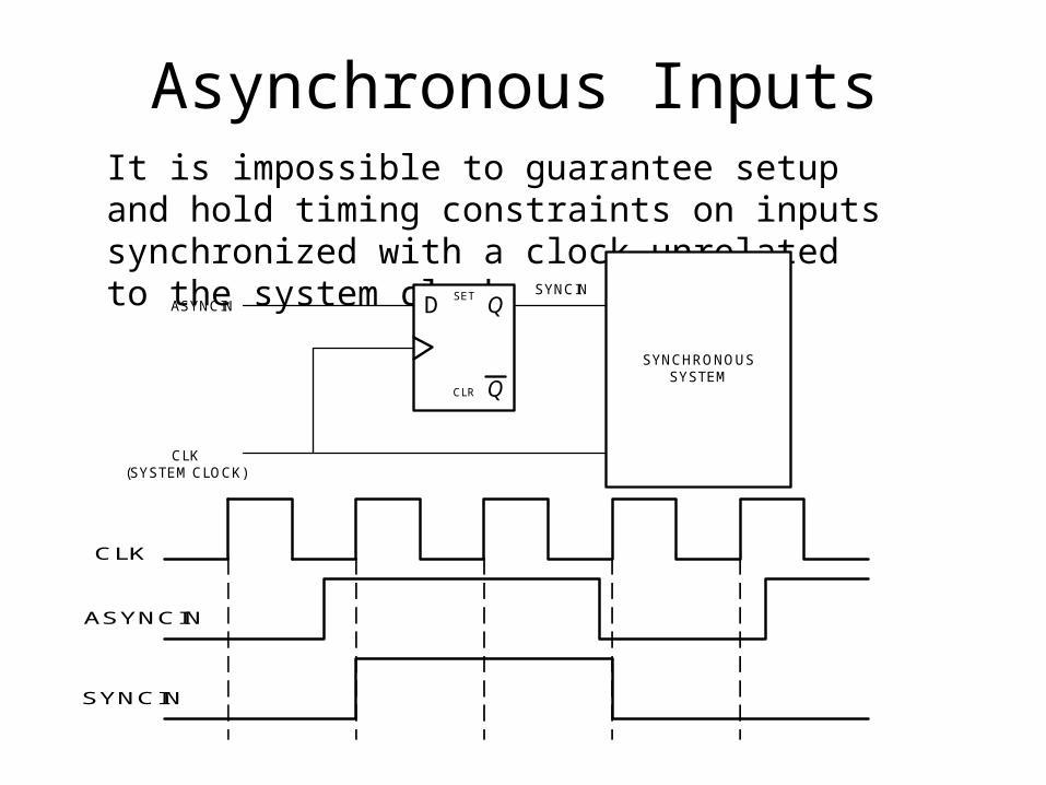
Asynchronous InputsIt is impossible to guarantee setup and hold timing constraints on inputs synchronized with a clock unrelated to the system clock
Q
QSET
CLR
DASYNCIN
CLK (SYSTEM CLOCK)
SYNCHRONOUS SYSTEM
SYNCIN
CLK
ASYNCIN
SYNCIN
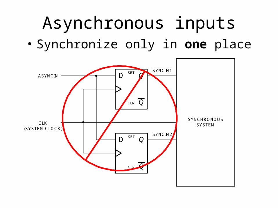
Asynchronous inputs• Synchronize only in one place
Q
QSET
CLR
DASYNCIN
CLK (SYSTEM CLOCK)
SYNCHRONOUS SYSTEM
SYNCIN1
Q
QSET
CLR
DSYNCIN2
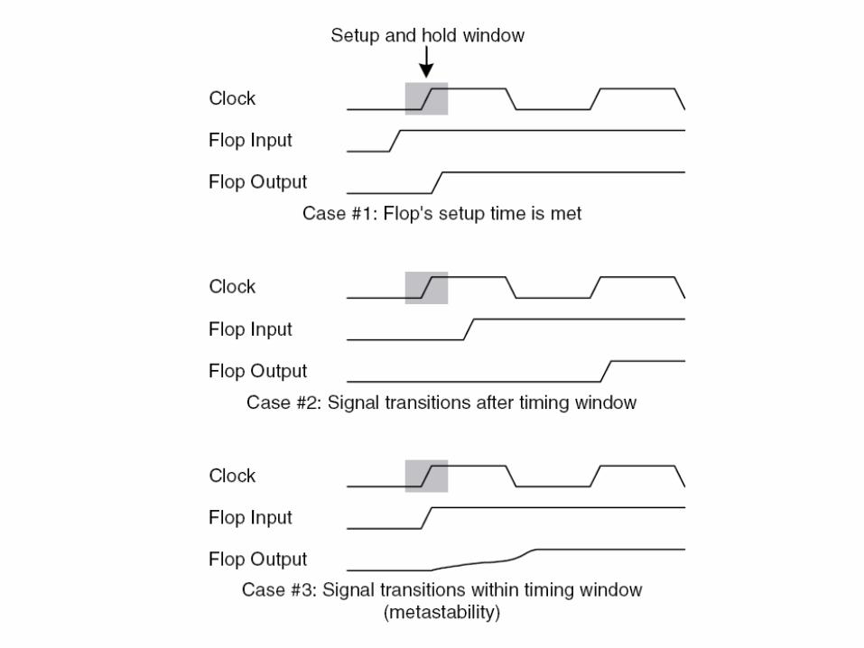
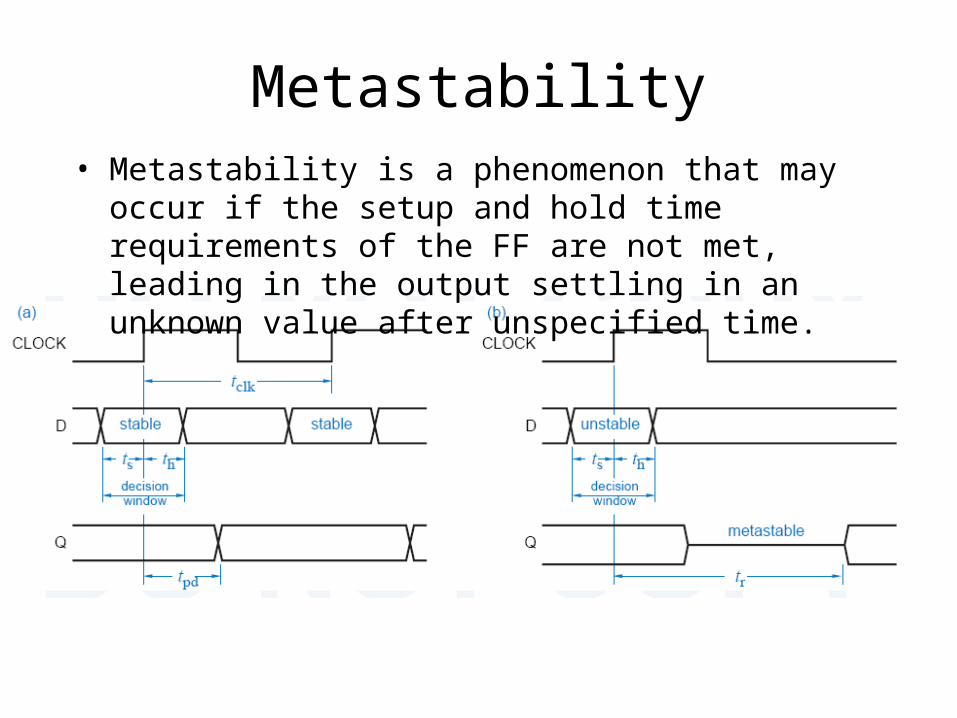
Metastability• Metastability is a phenomenon that may occur if the setup
and hold time requirements of the FF are not met, leading in the output settling in an unknown value after unspecified time.
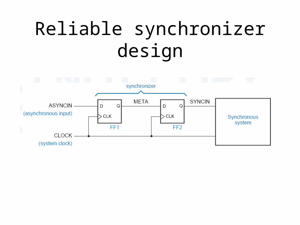
Reliable synchronizer design
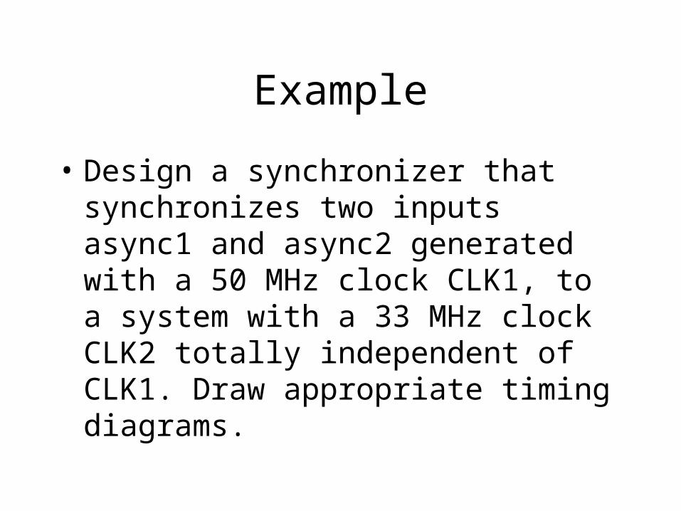
Example
• Design a synchronizer that synchronizes two inputs async1 and async2 generated with a 50 MHz clock CLK1, to a system with a 33 MHz clock CLK2 totally independent of CLK1. Draw appropriate timing diagrams.
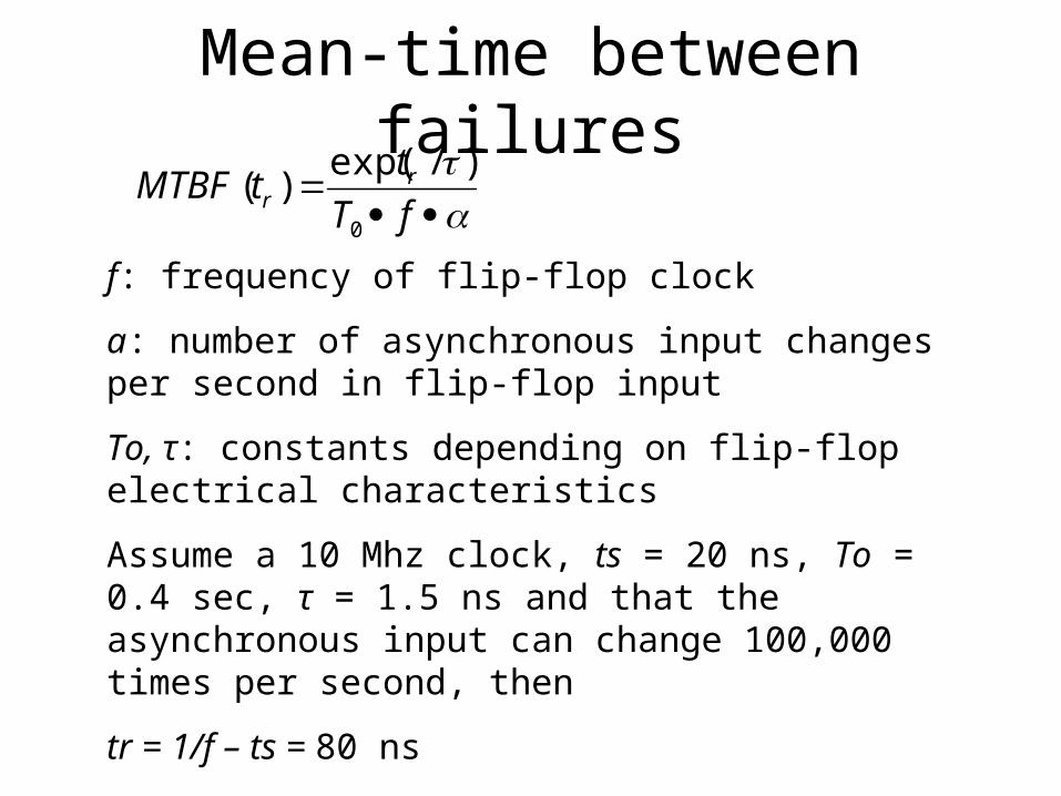
Mean-time between failures
fT
ttMTBF r
r0
)/exp()(
f: frequency of flip-flop clock
a: number of asynchronous input changes per second in flip-flop input
To, τ: constants depending on flip-flop electrical characteristics
Assume a 10 Mhz clock, ts = 20 ns, To = 0.4 sec, τ = 1.5 ns and that the asynchronous input can change 100,000 times per second, then
tr = 1/f – ts = 80 ns
MTBF(80ns) = exp(80/1.5)/0.4×10^7×10^5= 3.6×10^11 s

Cascaded synchronizer
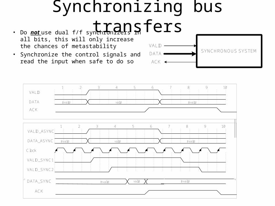
Synchronizing bus transfers• Do not use dual f/f synchronizers in all
bits, this will only increase the chances of metastability
• Synchronize the control signals and read the input when safe to do so
1 2 3 4 5 6 7 8 9 10
invalid valid invalid
VALID_ASYNC
DATA_ASYNC
Clock
VALID_SYNC1
VALID_SYNC2
DATA_SYNC invalid valid invalid
ACK
SYNCHRONOUS SYSTEMVALID
DATA
ACK
1 2 3 4 5 6 7 8 9 10
invalid valid invalid
VALID
DATA
ACK
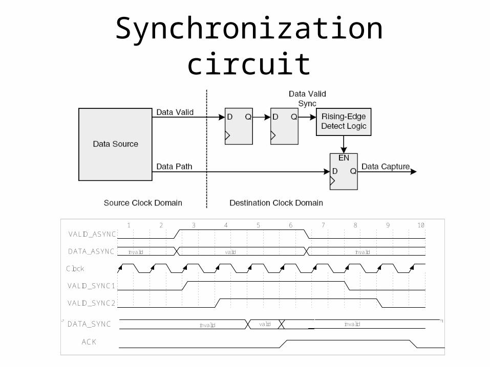
Synchronization circuit
1 2 3 4 5 6 7 8 9 10
invalid valid invalid
VALID_ASYNC
DATA_ASYNC
Clock
VALID_SYNC1
VALID_SYNC2
DATA_SYNC invalid valid invalid
ACK
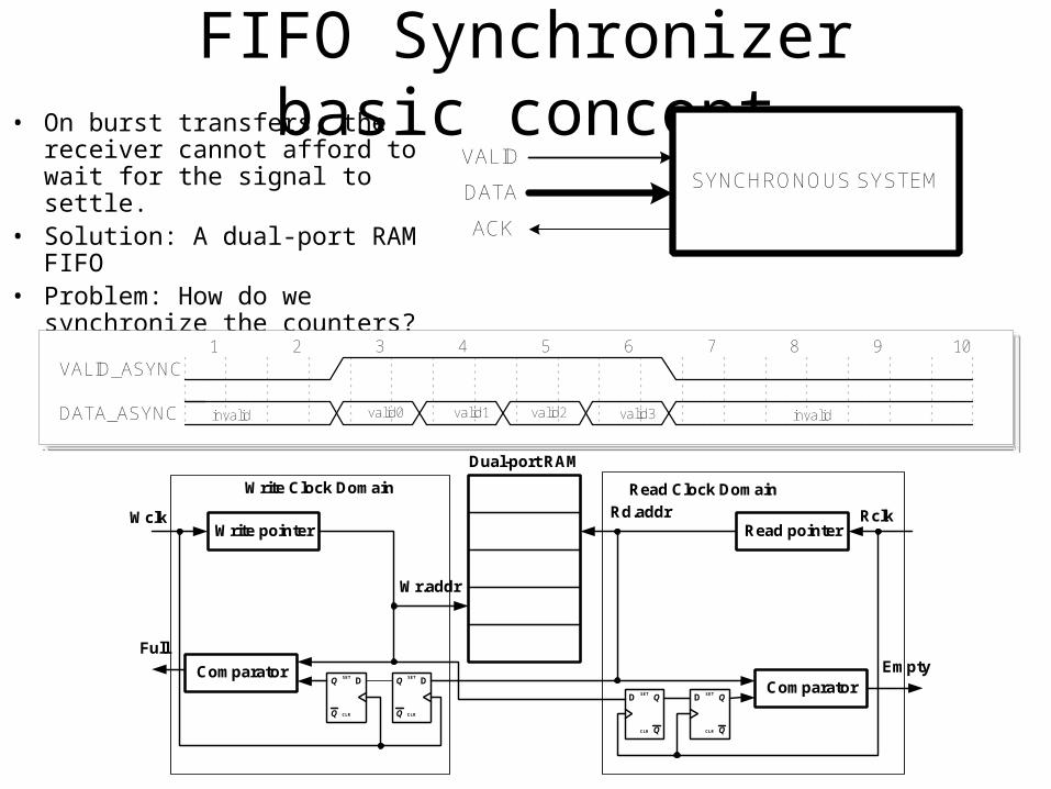
FIFO Synchronizer basic concept• On burst transfers, the receiver
cannot afford to wait for the signal to settle.
• Solution: A dual-port RAM FIFO• Problem: How do we synchronize
the counters?
SYNCHRONOUS SYSTEMVALID
DATA
ACK
1 2 3 4 5 6 7 8 9 10
invalid valid1 invalidvalid0 valid2 valid3
VALID_ASYNC
DATA_ASYNC
Wr.addr
Rd.addrWrite pointer Read pointer
Q
QSET
CLR
D
Q
QSET
CLR
D
ComparatorComparator
Empty
Write Clock Domain Read Clock Domain
Q
QSET
CLR
D
Q
QSET
CLR
D
Full
Wclk Rclk
Dual-port RAM
Summary• In order to avoid hazards and races, synchronous
design is used• In synchronous design a single common clock is
used and reset is only used for initialization• The only considerations in synchronous design are
the flip-flop setup and hold times, clock skew and asynchronous input synchronization
• Asynchronous inputs are commonly synchronized using 2 flip-flops clocked with the synchronous system clock
• Synchronization should only be done in one place• In bus transfers, synchronize only the control
signals or use a FIFO
Design trade-offs
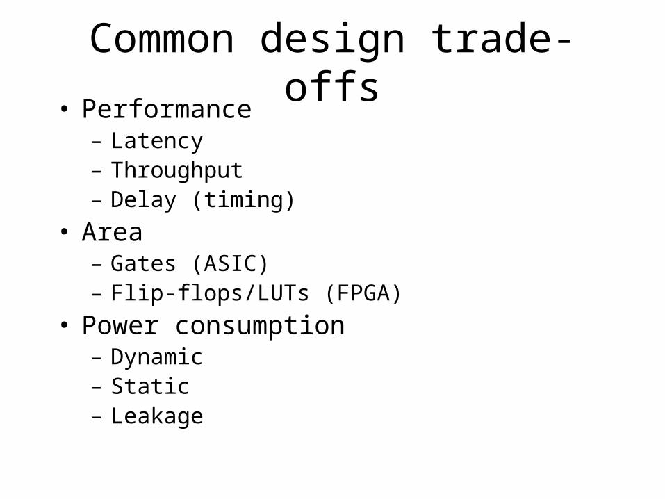
Common design trade-offs• Performance
– Latency– Throughput– Delay (timing)
• Area– Gates (ASIC)– Flip-flops/LUTs (FPGA)
• Power consumption– Dynamic– Static– Leakage
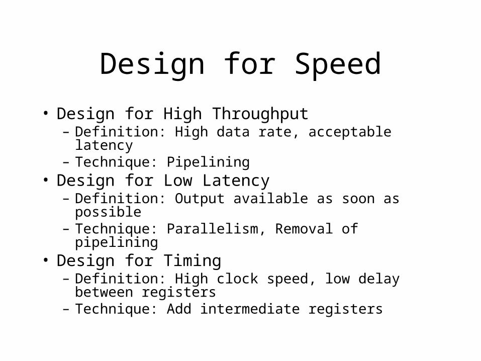
Design for Speed
• Design for High Throughput– Definition: High data rate, acceptable latency– Technique: Pipelining
• Design for Low Latency– Definition: Output available as soon as possible– Technique: Parallelism, Removal of pipelining
• Design for Timing– Definition: High clock speed, low delay between
registers– Technique: Add intermediate registers
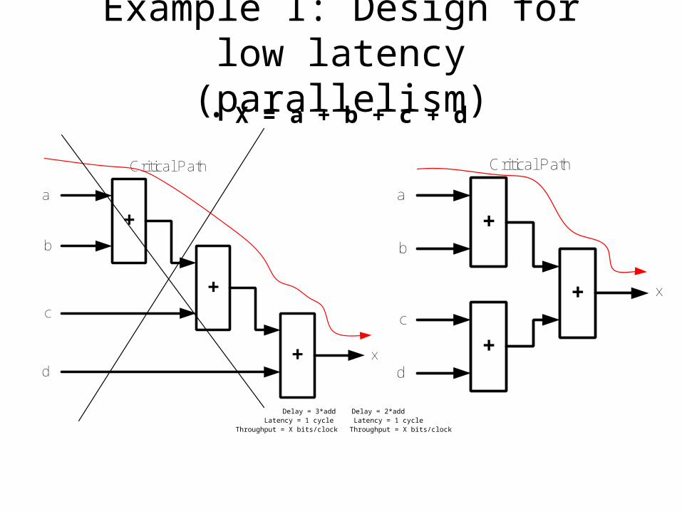
Example 1: Design for low latency (parallelism)• X = a + b + c + d
+
+
a
b
c
d
+ x
Critical Path
+
+
a
b
c
d
+
x
Critical Path
Delay = 3*add Delay = 2*addLatency = 1 cycle Latency = 1 cycle
Throughput = X bits/clock Throughput = X bits/clock
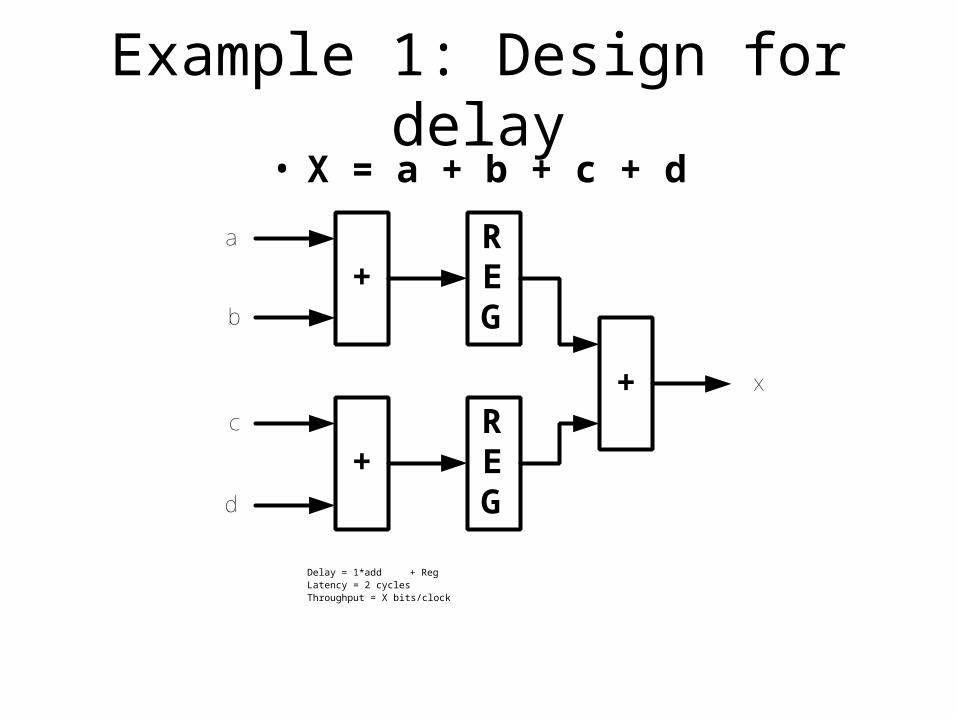
Example 1: Design for delay• X = a + b + c + d
REG
REG
a
b
c
d
+ x
+
+
Delay = 1*add + RegLatency = 2 cyclesThroughput = X bits/clock
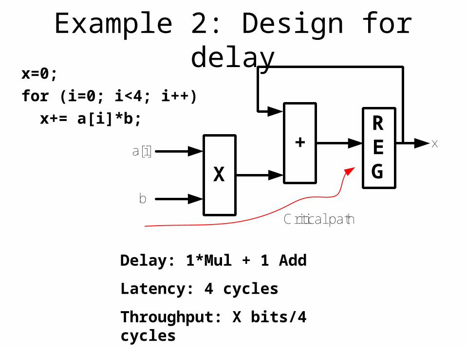
Example 2: Design for delayx=0;
for (i=0; i<4; i++)
x+= a[i]*b; REG
a[i]
b
+ x
X
Critical path
Delay: 1*Mul + 1 Add
Latency: 4 cycles
Throughput: X bits/4 cycles
Example 2: Design for latency
Example 2: Design for throughput
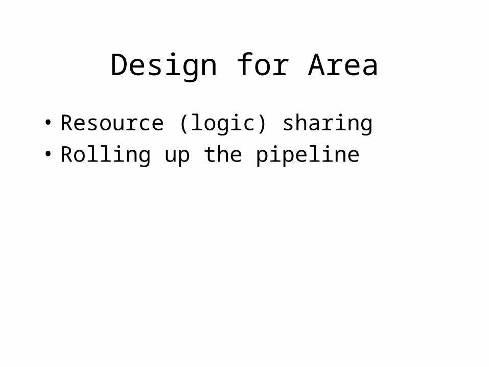
Design for Area
• Resource (logic) sharing
• Rolling up the pipeline
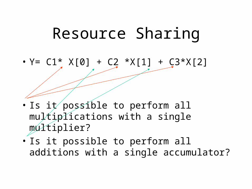
Resource Sharing
• Y= C1* X[0] + C2 *X[1] + C3*X[2]
• Is it possible to perform all multiplications with a single multiplier?
• Is it possible to perform all additions with a single accumulator?

Resource Sharing
X +
REG
REG
REG

Design for low-power
• Power components:• Dynamic power consumption (switching):
power consumed due to charging and discharging parasitic capacitances on gates and wires
• Static power consumption: Power consumed when no switching
• Leakage current power consumption:
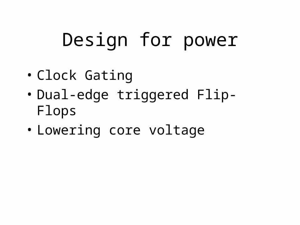
Design for power
• Clock Gating
• Dual-edge triggered Flip-Flops
• Lowering core voltage
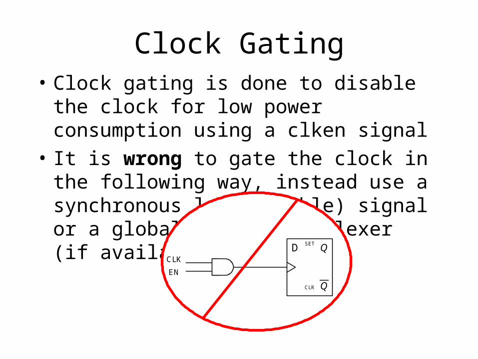
Clock Gating• Clock gating is done to disable the clock for
low power consumption using a clken signal
• It is wrong to gate the clock in the following way, instead use a synchronous load (enable) signal or a global clock multiplexer (if available)
Q
QSET
CLR
DCLK
EN
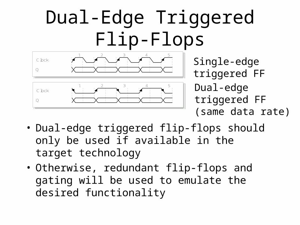
Dual-Edge Triggered Flip-Flops
• Dual-edge triggered flip-flops should only be used if available in the target technology
• Otherwise, redundant flip-flops and gating will be used to emulate the desired functionality
1 2 3 4 5
Clock
Q
1 2 3 4 5
Clock
Q
Single-edge triggered FF
Dual-edge triggered FF (same data rate)
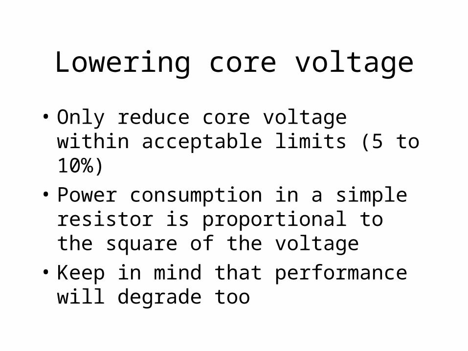
Lowering core voltage
• Only reduce core voltage within acceptable limits (5 to 10%)
• Power consumption in a simple resistor is proportional to the square of the voltage
• Keep in mind that performance will degrade too
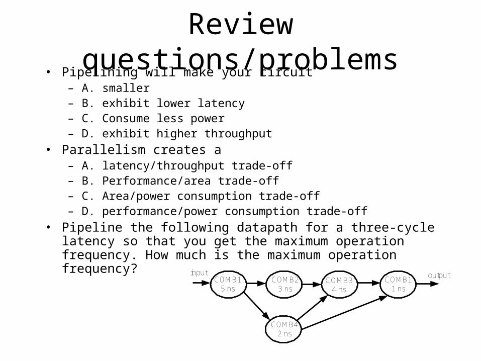
Review questions/problems• Pipelining will make your circuit
– A. smaller– B. exhibit lower latency– C. Consume less power– D. exhibit higher throughput
• Parallelism creates a– A. latency/throughput trade-off– B. Performance/area trade-off– C. Area/power consumption trade-off– D. performance/power consumption trade-off
• Pipeline the following datapath for a three-cycle latency so that you get the maximum operation frequency. How much is the maximum operation frequency?
COMB1 5 ns
COMB3 4 ns
COMB2 3 ns
COMB4 2 ns
COMB1 1 ns
input output


![59223623 Synchronous Digital Hierarchy[2]](https://img.pdfslide.us/doc/110x75/577d211d1a28ab4e1e9487ae/59223623-synchronous-digital-hierarchy2.jpg)