Embed Size (px)
Citation preview

DATA SHEET
Product specificationSupersedes data of 2001 Aug 15
2003 Nov 06
INTEGRATED CIRCUITS
TDA8020HLDual IC card interface

2003 Nov 06 2
Philips Semiconductors Product specification
Dual IC card interface TDA8020HL
FEATURES
• Two independent 6 contacts smart card interfaces
• Supply voltage to the cards: VCC = 5 V and ICC up to60 mA or 3 V ±5% and ICC up to 55 mA
• Integrated DC-to-DC converter (doubler, tripler orfollower) for allowing power supply from 2.7 to 6.5 V
• Independent supply voltage for interface signals (from1.5 to 6.5 V)
• Control and status via the I2C-bus
• Four possible devices in parallel due to two I2C-busaddress pins
• Electrical specifications according to ISO 7816 orEMV2000
• Automatic activation and deactivation sequences bymeans of integrated sequencers
• Automatic clock count and reset toggling during warm orcold reset
• Interrupt request output to the controller
• 6 kV ESD protection on cards contacts
• Automatic emergency deactivation in the event ofsupply drop-out, overload, overheating, card take-off orDC-to-DC malfunctioning
• Current limitation on pins CLK, RST, I/O and VCC
• Integrated voltage supervisor for power-on reset anddrop-out detection.
APPLICATIONS
• Set top boxes
• Banking terminals
• Internet terminals.
GENERAL DESCRIPTION
The TDA8020HL is a one-chip dual smart card interface.Controlled by the I2C-bus, it guarantees conformity toISO 7816 or EMV2000 with very few external components.
ORDERING INFORMATION
TYPE NUMBERPACKAGE
NAME DESCRIPTION VERSION
TDA8020HL/C1 LQFP32 plastic low profile quad flat package; 32 leads; body 7 × 7 × 1.4 mm SOT358-1
TDA8020HL/C2 LQFP32 plastic low profile quad flat package; 32 leads; body 7 × 7 × 1.4 mm SOT358-1
2003 Nov 06 3
Philips Semiconductors Product specification
Dual IC card interface TDA8020HL
QUICK REFERENCE DATA
SYMBOL PARAMETER CONDITIONS MIN. TYP. MAX. UNIT
Supplies
VDD supply voltage on pins VDD andVDDA
2.7 − 6.5 V
VDDI supply voltage for interface signals 1.5 − VDD V
IDD supply current VDD = 3.3 V; inactive mode − − 150 µA
VDD = 3.3 V; Power-down mode;2 cards activated; VCC1 = VCC2 = 5 V;ICC1 = ICC2 = 100 µA;CLK1 and CLK2 stopped
− − 2 mA
VDD = 3.3 V; active mode;VCC1 = VCC2 = 5 V;ICC1 + ICC2 = 80 mA;CLK1 = CLK2 = 5 MHz
− − 400 mA
VDD = 3.3 V; active mode;VCC1 = VCC2 = 3 V;ICC1 = ICC2 = 10 mA;CLK1 = CLK2 = 5 MHz
− − 80 mA
IDDA DC-to-DC converter supply current inactive mode; VDDA = 5 V;fxtal = 10 MHz
− − 0.1 mA
active mode; VDDA = 5 V;fxtal = 10 MHz; no load
− − 10 mA
Card supply
VCC1, VCC2 card supply voltage including ripple 5 V card; DC ICC < 60 mA 4.75 − 5.25 V
5 V card; AC current spikes of 40 nAs 4.65 − 5.25 V
3 V card; DC ICC < 55 mA 2.85 − 3.15 V
3 V card; AC current spikes of 40 nAs 2.76 − 3.20 V
Vripple(p-p) ripple voltage (peak-to-peak value) 20 kHz to 200 MHz − − 350 mV
ICC1, ICC2 card supply current 0 V to 5 V − − 60 mA
0 V to 3 V − − 55 mA
General
Vth1 threshold voltage for the supervisoron VDD
2.1 − 2.4 V
Vhys1 hysteresis on Vth1 50 − 100 mV
tde deactivation cycle duration 50 80 100 µs
Ptot continuous total power dissipation Tamb = −40 to +85 °C − − 0.50 W
Tamb ambient temperature TDA8020HL/C1 −30 − +85 °CTDA8020HL/C2 −40 − +85 °C

2003 Nov 06 4
Philips Semiconductors Product specification
Dual IC card interface TDA8020HL
BLOCK DIAGRAM
handbook, full pagewidth
I2C-BUSAND
REGISTERS
LEVELSHIFTERS
INTERNAL OSCILLATOR
SUPPLY SUPERVISORVOLTAGE REFERENCE
DC-to-DCCONVERTER
CLOCKCIRCUITRY
SEQUENCER1
TDA8020HL
CARD1DRIVERS
SAP20 14 19 15 17
16
13
3
5
4
2
32
1
9
11
10
8
6
7
1218
31
28
27
26
29
25
22
21
24
23
30
VDD
SAM SBP SBM
VDDA
VUPCDEL
IRQ
SDA
SAD0
SAD1
SCL
AGND GND
CLK1
RST1
VCC1
CGND1
I/O1
PRES1
CLOCKCIRCUITRY
SEQUENCER2
CARD2DRIVERS
CLK2
RST2
VCC2
CGND2
I/O2
PRES2VDDI
I/O2uC
CLKIN2
CLKIN1
I/O1uC
FCE834
Fig.1 Block diagram.

2003 Nov 06 5
Philips Semiconductors Product specification
Dual IC card interface TDA8020HL
PINNING
SYMBOL PIN TYPE DESCRIPTION
PRES1 1 I card 1 presence contact input (active HIGH)
CGND1 2 supply ground connection output to card 1 (C5 contact)
CLK1 3 O clock output to card 1 (C3 contact)
VCC1 4 supply supply voltage output to card 1 (C1 contact); decouple to pin CGND1 with2 × 100 nF capacitors with ESR < 100 mΩ
RST1 5 O reset output to card 1 (C2 contact)
I/O2 6 I/O I/O contact to card 2 (C7 contact); internal 15 kΩ pull-up resistance topin VCC2
PRES2 7 I card 2 presence contact input (active HIGH)
CGND2 8 supply ground connection output to card 2 (C5 contact)
CLK2 9 O clock output to card 2 (C3 contact)
VCC2 10 supply supply voltage output to card 2 (C1 contact); decouple to pin CGND2 with2 × 100 nF capacitors with ESR < 100 mΩ
RST2 11 O reset output to card 2 (C2 contact)
GND 12 supply ground connection
VUP 13 I/O output of DC-to-DC converter; a 220 nF capacitor with ESR < 100 mΩ mustbe connected to pin AGND
SAP 14 I/O capacitor connection for the DC-to-DC converter; a 220 nF capacitor withESR < 100 mΩ must be connected between pins SAP and SAM
SBP 15 I/O capacitor connection for the DC-to-DC converter; a 220 nF capacitor withESR < 100 mΩ must be connected between pins SBP and SBM
VDDA 16 supply analog supply voltage for the DC-to-DC converter
SBM 17 I/O capacitor connection for the DC-to-DC converter; a 220 nF capacitor withESR < 100 mΩ must be connected between pins SBP and SBM
AGND 18 supply analog ground for the DC-to-DC converter
SAM 19 I/O capacitor connection for the DC-to-DC converter; a 220 nF capacitor withESR < 100 mΩ must be connected between pins SAP and SAM
VDD 20 supply power supply voltage
SCL 21 I serial clock input of I2C-bus (open drain)
SDA 22 I/O serial data input/output of I2C-bus (open drain)
SAD0 23 I I2C-bus address selection input 0
SAD1 24 I I2C-bus address selection input 1
IRQ 25 O interrupt request output to host (open drain; active LOW)
CLKIN1 26 I external clock input for card 1
I/O1uC 27 I/O I/O connection to host for card 1; internal 11 kΩ pull-up resistor to VDDI
I/O2uC 28 I/O I/O connection to host for card 2; internal 11 kΩ pull-up resistor to VDDI
CLKIN2 29 I external clock input for card 2
CDEL 30 I/O delay capacitor connection for the voltage supervisor (1 ms per 2 nF)
VDDI 31 I interface signals reference supply voltage
I/O1 32 I/O I/O contact to card 1 (C7 contact); internal 14 kΩ pull-up resistor to VCC1

2003 Nov 06 6
Philips Semiconductors Product specification
Dual IC card interface TDA8020HL
handbook, full pagewidth
TDA8020HL
FCE833
1
2
3
4
5
6
7
8
24
23
22
21
20
19
18
17
9 10 11 12 13 14 15 16
32 31 30 29 28 27 26 25
PRES1
CGND1
CLK1
VCC1
RST1
I/O2
PRES2
CGND2
SAD1C
LK2
VC
C2
RS
T2
GN
D
VU
P
SA
P
SB
P
VD
DA
SAD0
SDA
SCL
VDD
SAM
AGND
SBMIR
Q
CLK
IN1
I/O
1uC
I/O
2uC
CLK
IN2
CD
EL
VD
DI
I/O
1
Fig.2 Pin configuration.

2003 Nov 06 7
Philips Semiconductors Product specification
Dual IC card interface TDA8020HL
FUNCTIONAL DESCRIPTION
Throughout this specification, it is assumed that the readeris familiar with ISO 7816 terminology.
Supply
The TDA8020HL operates with a supply voltage from2.7 to 6.5 V. An integrated voltage supervisor ensures thatno spike appears on cards contacts during power-on or off.The supervisor also initializes the device, and forces anautomatic emergency deactivation of the contacts in theevent of a supply drop-out.
As long as the supply voltage is below the thresholdvoltage Vth1, the capacitor CDEL remains uncharged. Whenthe supply voltage reaches Vth1 and Vhys1, then CDEL ischarged with a small current source of approximately 2 µA.When the voltage on CDEL reaches Vth2, then thesupervisor is no longer active. As long as the supervisor isactive (pin IRQ is LOW), bit SUPL in the status register isset. When pin IRQ goes HIGH the voltage supervisorbecomes inactive (see Fig.3).
Separate supply pins are used for the DC-to-DC converter,allowing specific decoupling for counteracting the noisethe switching transistors may induce on the supply.
A specific reference supply voltage, VDDI, is used for theinterface signals CLKIN1, CLKIN2, I/O1uC, I/O2uC,SAD0, SAD1, SCL, SDA and IRQ, which can be lowerthan VDD (minimum 1.5 V), thus allowing direct control witha low voltage supplied device.
Pins SCL, SDA and IRQ are open-drain outputs, and maybe externally pulled up to a voltage higher than VDD.
handbook, full pagewidth
tw tw
FCE835
BUS OK BUS NOT RESPONDING
BUS NOTRESPONDING
BUS NOT RESPONDING BUS OK
status readafter event
VDD
Vth1 + Vhys1Vth1
Vth2VCDEL
IRQ
Fig.3 Voltage supervisor.

2003 Nov 06 8
Philips Semiconductors Product specification
Dual IC card interface TDA8020HL
DC-to-DC converter
VCC1 is the supply voltage for card 1 contacts and VCC2 isthe supply voltage for card 2 contacts. Card 1 and card 2may be independently powered-down, powered at 5 V orpowered at 3 V. A capacitor type step-up converter is usedfor generating these voltages. This step-up converter actseither as a doubler, tripler or follower. An hysteresis of100 mV is present on the different threshold voltages.
If VCC is the maximum value of VCC1 and VCC2, then thereare 5 possible situations:
• VDD < 3.4 V and VCC = 3 V: in this case, the DC-to-DCconverter acts as a doubler with a regulation ofapproximately 4.0 V
• VDD < 3.4 V and VCC = 5 V: in this case, the DC-to-DCconverter acts as a tripler with a regulation ofapproximately 5.5 V
• VDD > 3.5 V and VCC = 3 V: in this case, the DC-to-DCconverter acts as a follower: VDD is applied on VUP
• 5.8 V > VDD > 3.5 V and VCC = 5 V: in this case, theDC-to-DC converter acts as a doubler with a regulationof approximately 5.5 V
• VDD > 5.9 V and VCC = 5 V: in this case, the DC-to-DCconverter acts as a follower and VDD is applied on VUP.
The output voltage, VUP, is fed internally to the VCCgenerators. VCC1, VCC2 and CGND1, CGND2 are used asa reference for all other cards contacts.
The sum of ICC1 and ICC2 shall not exceed 80 mA, whichmeans that when a card is drawing its maximum current(around 60 mA at VCC = 5 V, 55 mA at VCC = 3 V), theother card should be set in low power consumption mode(less than 20 or 25 mA). Note that during the card Adviceto Receive (ATR) process, the current may be maximum;so, a card should only be activated if the other card drawsless than 20 or 25 mA. The DC-to-DC converter is suppliedvia separate supply pins VDDA and AGND to allowdecoupling separate from the other supply pins.
During normal operation or activation, each card is allowedto draw independently a current of up to 60 mA atVCC = 5 V or up to 55 mA at VCC = 3 V, with a supplyvoltage from 2.7 V up to 6.5 V provided the sum ofICC1 and ICC2 does not exceed 80 mA.
If VDD > 3 V, for 5 V cards, then both cards can draw up to60 mA at the same time.
If VDD > 3 V, for 3 V cards, then both cards can draw up to55 mA at the same time.
I2C-bus
A 400 kHz I2C-bus slave interface is used for configuringthe device and reading the status.
I2C-BUS PROTOCOL
The I2C-bus is for 2-way, 2-line communication betweendifferent ICs or modules. The serial bus consists of twobidirectional lines; one for data (SDA), and one for theclock (SCL).
Both the SDA and SCL lines must be connected to apositive supply voltage via a pull-up resistor.
The following protocol has been defined:
• Data transfer may be initiated only when the bus is notbusy
• During data transfer, the data line must remain stablewhenever the clock line is HIGH. Changes in the dataline while the clock line is HIGH will be interpreted ascontrol signals.
BUS CONDITIONS
The following bus conditions have been defined:
• Bus not busy: both data and clock lines remain HIGH
• Start data transfer: a change in the state of the data line,from HIGH-to-LOW, while the clock is HIGH, defines theSTART condition
• Stop data transfer: a change in the state of the data line,from LOW-to-HIGH, while the clock is HIGH, defines theSTOP condition
• Data valid: the state of the data line represents validdata when, after a START condition, the data line isstable for the duration of the HIGH period of the clocksignal. There is one clock pulse per data bit.
DATA TRANSFER
Each data transfer is initiated with a START condition andterminated with a STOP condition.
Data transfer is unlimited in the read mode. Theinformation is transmitted in bytes and each receiveracknowledges with a ninth bit.
The TDA8020HL operates in standard mode (100 kHzclock rate) and fast mode (400 kHz clock rate) defined inthe I2C-bus specification.
By definition, a device that sends a signal is called atransmitter, and the device which receives the signal iscalled a receiver. The device which controls the signal is

2003 Nov 06 9
Philips Semiconductors Product specification
Dual IC card interface TDA8020HL
called the master. The devices that are controlled by themaster are called slaves.
Each byte is followed by one HIGH-level acknowledge bitasserted by the transmitter. The master generates anextra acknowledge related clock pulse. The slave receiverwhich is addressed is obliged to generate an acknowledgeafter the reception of each byte.
The master receiver must generate an acknowledge afterthe reception of each byte that has been clocked out of theslave transmitter.
The device that acknowledges has to pull-down the SDAline during the acknowledge clock pulse in such a way thatthe SDA line is stable LOW during the HIGH period of theacknowledge related clock pulse.
Set-up and hold times must be taken into account.A master receiver must signal an end of data to the slave
transmitter by not generating an acknowledge on the lastbyte that has been clocked out of the slave. In this event,the transmitter must leave the data line HIGH to enable themaster generation of the STOP condition.
See Chapter “Characteristics” for timing information.
DEVICE ADDRESSING
Each device has 2 different addresses, one for each card.
An application can use up to four devices in parallel by theuse of address selection pins SAD0 and SAD1.Pins SAD0 and SAD1 are externally hardwired to VDD orGND; SAD0 specifies address bit A0, SAD1 specifiesaddress bit A1; Address bit R/W specifies either read orwrite operation: logic 1 = Read, logic 0 = Write (seeTables 1 and 2).
Table 1 Proposed device address bit allocations
Table 2 Proposed I2C-bus addresses for 4 devices in parallel
DeviceAddress bits
7 6 5 4 3 2 1 0
TDA8020HL 0 1 0 0 0/1 A1 A0 R/W
PIN SAD1 PIN SAD0 CARD 1 CARD 2
LOW LOW 40H 48H
LOW HIGH 42H 4AH
HIGH LOW 44H 4CH
HIGH HIGH 46H 4EH

2003 Nov 06 10
Philips Semiconductors Product specification
Dual IC card interface TDA8020HL
WRITE SEQUENCE
The write sequence is as follows:
1. START condition
2. Byte 1: ADDRESS plus write command
3. ACK: acknowledge
4. Byte 2: CONTROL byte; see Table 3
5. ACK: acknowledge
6. STOP condition.
Table 3 CONTROL byte bits (all bits cleared after power-on)
All frequency changes are synchronous, thus ensuring that no pulse is shorter than 45% of the smallest period. For cardspower reduction modes, CLKIN may be stopped after switching to stop LOW or stop HIGH. CLKIN should be restartedbefore leaving this mode and the selected frequency must not be changed during a CLK stop mode.
A correct duty factor can not be guaranteed in the CLKIN configuration, as it depends on the duty factor of the CLKINsignal.
BIT NAME DESCRIPTION
0 START/STOP when set, initiates an activation and a cold reset procedure; when reset, initiates a deactivationsequence
1 WARM when set, initiates a warm reset procedure; automatically reset by hardware when the card startsanswering or when the card is declared mute (once the status has been read)
2 3 V / 5 V when set; VCC = 3 V; when reset; VCC = 5 V
3 PDOWN when set, the configuration defined by bit CLKPD is applied to pin CLK, and the circuit enters thePower-down mode; when reset, the circuit goes back to normal (active) mode
4 CLKPD when set, CLK is stopped HIGH during Power-down mode; when reset, CLK is stopped LOW inPower-down mode
5 CLKSEL1 determine the clock to the card in active mode:
6 CLKSEL2 00: CLKIN/8
01: CLKIN/4
10: CLKIN/2
11: CLKIN
7 I/OEN when set, I/O data is transferred on pin I/OuC; when reset, pin I/OuC is high-impedance

2003 Nov 06 11
Philips Semiconductors Product specification
Dual IC card interface TDA8020HL
READ STATUS SEQUENCE
The read status sequence is as follows:
1. START condition
2. Byte 1: ADDRESS plus read command
3. ACK: acknowledge
4. Byte 2: STATUS byte; see Table 4
5. ACK: acknowledge
6. STOP condition.
Table 4 STATUS byte bits (all bits cleared after power-on)
When one of the bits PRESL, MUTE, EARLY and PROT is set, then IRQ goes LOW until the status byte has been read.After power-on, bit SUPL is set until the status byte has been read, and IRQ is LOW until the supervisor becomesinactive.
BIT NAME DESCRIPTION
0 PRES set when the card is present; reset when the card is not present
1 PRESL set when the card has been inserted or extracted; reset when the status has been read
2 I/O set when I/O is HIGH; reset when I/O is LOW
3 SUPL set when the supervisor has signalled a fault; reset when the status has been read
4 PROT set when an overload or an overheating has occurred during a session; reset when the statushas been read
5 MUTE set during ATR when the selected card has not answered during the ISO 7816 time slots; resetwhen the status has been read
6 EARLY set during ATR when the selected card has answered too early; reset when the status has beenread
7 ACTIVE set if the card is active; reset if the card is inactive
Sequencers and clock counter
Two sequencers are used to ensure activation anddeactivation sequences according to ISO 7816 andEMV 2000, even in the event of an emergency (cardremoval during transaction, supply drop-out and hardwareproblem).
The sequencers are clocked by the internal oscillator.
The activation of a card is initiated by setting the cardselect bit and the start bit within the control register. This isonly possible if the card is present and if the voltagesupervisor is not active.
During activation the DC-to-DC converter is initiated(except if another card is already powered up or ifVDD = 5 V and VCC = 3 V). VCC then goes high to theselected voltage (3 or 5 V), the I/O lines are then enabledand the clock is started with RST LOW.
DEVICE TYPE TDA8020HL/C1:
1. If a start bit is detected on the I/O during the first200 CLK pulses, it is ignored and the count continues.
2. If a start bit is detected between 200 and 352 CLKpulses, bit EARLY is set in the status register.
3. If the card starts responding within 41950 CLK pulses,RST remains LOW.
4. If the card has not responded within 41950 CLKpulses, then RST goes HIGH.
5. If a start bit is detected within 352 CLK pulses, bitEARLY is set in the status register.
6. If the card does not respond within the next 41950CLK pulses, bit MUTE is set within the status register.This initiates a warm reset command.
7. If the card responds within the correct window period,the CLK count is stopped and the system controllermay send commands to the card.

2003 Nov 06 12
Philips Semiconductors Product specification
Dual IC card interface TDA8020HL
Deactivation is initiated either by the system controller(reset bit START), or automatically in the event of ahardware problem or supply drop-out. With a supplydrop-out both cards are deactivated at the same time.
During deactivation, RST goes LOW, the clock is stoppedand the I/O lines go LOW. VCC then goes low with acontrolled slope and the DC-to-DC converter is stopped ifno card is active.
Outside a session, cards contacts are forced lowimpedance to CGND.
DEVICE TYPE TDA8020HL/C2:
1. If a start bit is detected on the I/O during the first200 CLK pulses, it is ignored and the count continues.
2. If a start bit is detected whilst RST is LOW (between200 and 42100 CLK pulses), bits EARLY and MUTEare set in the status register; RST will remain LOW; thesoftware decides whether to accept the card or not.
3. If no start bit has been detected until after 42100 CLKpulses, RST is set to logic 1.
4. If a start bit is detected within 370 CLK pulses, bitEARLY is set in the status register.
5. If the card does not respond within the next 42100CLK pulses, bit MUTE is set within the status register.This initiates a warm reset command.
6. If the card responds within the correct window period,the CLK count is stopped and the system controllermay send commands to the card.
Deactivation is initiated either by the system controller(reset bit START), or automatically in the event of ahardware problem or supply drop-out. With a supplydrop-out both cards are deactivated at the same time.
During deactivation, RST goes LOW, the clock is stoppedand the I/O lines go LOW. VCC then goes low with acontrolled slope and the DC-to-DC converter is stopped ifno card is active.
Outside a session, cards contacts are forced lowimpedance to CGND.
Activation sequence
When the cards are inactive, VCC, CLK, RST and I/O areLOW, with low impedance with respect to CGND. TheDC-to-DC converter is stopped.
When everything is satisfactory (voltage supply, cardpresent and no hardware problems), the system controllermay initiate a card present activation sequence(see Fig.4):
1. The internal oscillator changes to its high frequency(t0).
2. The DC-to-DC converter is started (t1). If one card wasalready active, then the DC-to-DC converter wasalready on, and nothing more occurs at this step.
3. VCC starts rising from 0 to 5 or 3 V with a controlledrise time of 0.14 V/µs typical (t2).
4. I/O rises to VCC (t3); internal 14 kΩ pull-up resistors toVCC.
5. CLK is sent to the card and RST is enabled (t4 = tact).
If the card does not respond within the first 42100 CLKcycles, then RST is raised HIGH (t5).
The sequencer is clocked by fint/64 which leads to a timeinterval T of 25 µs typical. Thus t1 = 0 to T/64;t2 = t1 + 3T/2; t3 = t1 + 7T/2 and t4 = t1 + 4T.

2003 Nov 06 13
Philips Semiconductors Product specification
Dual IC card interface TDA8020HL
Deactivation sequence
When the session is completed, the microcontroller resets bit START/STOP to logic 0 (t10). The circuit then executes anautomatic deactivation sequence (see Fig.5):
1. Card reset (RST falls LOW) (t11)
2. Clock is stopped (t12)
3. I/O falls to 0 V (t13)
4. VCC falls to 0 V with a controlled slew rate (t14)
5. The DC-to-DC converter is stopped (if both cards are inactive) and CLK, RST, VCC and I/O become low impedanceto CGND (t15)
6. The internal oscillator changes to its low frequency if both cards are inactive (t15).
t11 = t10 + T/64; t12 = t11 + T/2; t13 = t11 + T; t14 = t11 + 3T/2; t15 = t11 + 7T/2.
The deactivation time tde is the time that VCC needs to drop below 0.4 V from START/STOP to logic 0 (t10).
VUP
VCC
I/O
CLK
RST
handbook, full pagewidth
START/STOP
t0 t1 t2 t3 t4 t5FCE837
ATR
Fig.4 Activation sequence.

2003 Nov 06 14
Philips Semiconductors Product specification
Dual IC card interface TDA8020HL
handbook, full pagewidth
tde
t10 t11 t12 t13 t14 t15
VUP
VCC
I/O
CLK
RST
START/STOP
FCE836
Fig.5 Deactivation sequence.
VCC buffers
Each card is supplied by a separate VCC buffer. Bothbuffers are supplied by the same multimode capacitiveDC-to-DC converter.
In all modes (follower, doubler and tripler), the DC-to-DCconverter is able to deliver 80 mA over the whole VDDrange (2.7 to 6.5 V) or 120 mA if VDD > 3 V.
The current in each VCC buffer is limited internally toaround 90 mA. When one of the buffers reaches this limit,an automatic deactivation sequence is performed.
Each VCC supply voltage should be decoupled by an ESRcapacitor with a value of between 100 and 200 nF. If thecard socket is not very close to the device, one capacitorshould be connected close to the device, and a secondone connected close to card contact C1.
Protections
The current on pin CLK is limited to within the range+70 mA and −70 mA.
The current on pin RST is limited to within the range+20 mA and −20 mA; if the current reaches this value with
RST LOW, then an emergency deactivation sequence isperformed, IRQ is pulled LOW and bit PROT is set in thestatus register.
The current on pins I/O is limited to within the range+15 mA and −15 mA.
The current on VCC is limited to 90 mA; if ICC reaches thisvalue, then an emergency deactivation sequence isperformed, IRQ is pulled LOW and bit PROT is set in thestatus register.
In the event of overcurrent on VCC, card take-off during asession, overheating, or overcurrent on RST, then theTDA8020HL performs an automatic emergencydeactivation sequence on the corresponding card, resetsbit START/STOP and pulls pin IRQ LOW.
In the event of overheating or supply drop-out, orDC-to-DC converter out of specification, the TDA8020HLperforms an automatic emergency deactivation sequenceon both cards, resets both bits START/STOP and pullspin IRQ LOW.

2003 Nov 06 15
Philips Semiconductors Product specification
Dual IC card interface TDA8020HL
Clock inputs and data inputs/outputs to the system controller
CLKIN1 is the input clock for card 1, CLKIN2 for card 2. They may be driven separately from the system controller, or betied together externally and driven by the same signal.
I/O1uC is the data signal to or from card 1, I/O2uC to or from card 2. They can be driven separately from the systemcontroller, in which case both bits I/OEN may be set to logic 1. They can also be driven by the same signal, whichrequires them to be tied together externally, but each bit I/OEN has to be set or reset according to the addressed card.
LIMITING VALUESIn accordance with the Absolute Maximum Rating System (IEC 60134).
Notes
1. HBM: EIA/JESD22-A 114-B; June 2000.
2. All card contacts are protected against any short-circuit with any other card contact.
3. MM: EIA/JESD22-A 115-A; October 1997.
HANDLING
Inputs and outputs are protected against electrostatic discharge in normal handling. However it is good practice to takenormal precautions appropriate to handling MOS devices (see “Handling MOS devices”).
THERMAL CHARACTERISTICS
SYMBOL PARAMETER CONDITION MIN. MAX. UNIT
VDD supply voltage on pins VDD and VDDA −0.5 +6.5 V
VDDI supply voltage for interface signals −0.5 +6.5 V
Vn input voltage
on pins SAP, SAM, SBP, SBM and VUP −0.5 +7.5 V
on pins SDA and SCL −0.5 +6.5 V
on all other pins −0.5 VDD + 0.5 V
Ptot total power dissipation Tamb = −40 °C to +85 °C − 500 mW
Tstg storage temperature −55 +150 °CTj junction temperature − 125 °CVesd electrostatic discharge voltage HMB; note 1
all card contact pinswithin the typicalapplication; note 2
−6 +6 kV
pins VDDA and VDDI −0.5 +0.5 kV
all other pins −2 +2 kV
MM; note 3
all pins −200 +200 V
SYMBOL PARAMETER CONDITIONS VALUE UNIT
Rth(j-a) thermal resistance from junction to ambient in free air 80 K/W

2003 Nov 06 16
Philips Semiconductors Product specification
Dual IC card interface TDA8020HL
CHARACTERISTICSVDD = 3.3 V; VDDI = 1.5 V; fCLKIN1 = fCLKIN2 = 10 MHz; GND = 0 V; Tamb = 25 °C.
SYMBOL PARAMETER CONDITIONS MIN. TYP. MAX. UNIT
Temperature
Tamb ambient temperature TDA8020HL/C1 −30 − +85 °CTDA8020HL/C2 −40 − +85 °C
Supply
VDD supply voltage on pins VDDand VDDA
2.7 − 6.5 V
IDD supply current (IDD and IDDA) inactive mode − − 150 µA
Power-down mode; 2 cardsactivated; VCC1 = VCC2 = 5 V;ICC1 = ICC2 = 100 µA; CLK1 andCLK2 stopped
− − 2.5 mA
active mode; VCC1 = VCC2 = 5 V;ICC1 + ICC2 = 80 mA;CLK1 = CLK2 = 5 MHz
− − 300 mA
active mode; VCC1 = VCC2 = 3 V;ICC1 = ICC2 = 10 mA;CLK1 = CLK2 = 5 MHz
− − 80 mA
VDDI supply voltage for interfacesignals
1.5 − VDD V
IDDI supply current for interfacesignals
− − 120 µA
Vth1 threshold voltage forsupervisor on VDD
falling 2.1 − 2.4 V
Vhys1 hysteresis on Vth1 50 − 100 mV
Vth2 threshold voltage onpin CDEL
− 1.38 − V
VCDEL voltage on pin CDEL − − VDD + 0.3 V
ICDEL output current at pin CDEL pin grounded (charge) − −2 − µA
VCDEL = VDD (discharge) − 5 − mA
tW width of the internal ALARMpulse
CCDEL = 22 nF − 10 − ms
DC-to-DC converter
fint internal oscillator frequency 2 2.5 3.2 MHz
VUP voltage on pin VUP at least one 5 V card − 5.5 − V
both 3 V cards − 4 − V
Vdt detection voltage for doubler,tripler and follower selection
− 3.4 − V
2003 Nov 06 17
Philips Semiconductors Product specification
Dual IC card interface TDA8020HL
Card supply voltages (pins V CC1 and VCC2); note 1
VCC(inactive) output voltage in inactivemode
no load 0 − 0.1 V
Iinactive = 1 mA 0 − 0.3 V
ICC(inactive) output current from VCCwhen inactive
pin grounded − − −1 mA
VCC(active) output voltage in activemode including ripple
ICC < 60 mA; 5 V card;ICC1 + ICC2 < 80 mA;2.7 V < VDD < 6.5 V
4.75 5 5.25 V
ICC < 55 mA; 3 V card;ICC1 + ICC2 < 80 mA;2.7 V < VDD < 6.5 V
2.8 3 3.2 V
current pulses of 40 nAs withI < 200 mA and t < 400 ns;f < 20 MHz; 5 V card
4.6 − 5.4 V
current pulses of 24 nAs withI < 200 mA and t < 400 ns;f < 20 MHz; 3 V card
2.76 − 3.24 V
VCC(load) output voltage when bothcard interfaces fully loaded
active mode; VDD > 3 V;ICC1 < 60 mA; ICC2 < 60 mA;5 V cards
4.6 − 5.4 V
active mode; VDD > 3 V;ICC < 55 mA; ICC2 < 55 mA;3 V cards
2.76 − 3.24 V
ICC(max) maximum output current from 0 to 5 V (5 V card); the othercard at full load; VDD > 3 V
− − −60 mA
from 0 to 3 V (3 V card); the othercard at full load; VDD > 3 V
− − −55 mA
ICC(sc) short-circuit current VCC shorted to GND − − −100 mA
Vripple(p-p) ripple voltage (peak-to-peakvalue)
from 20 kHz to 200 MHz − − 350 mV
SR slew rate up or down for 5 V card (maximumcapacitance is 300 nF)
0.08 0.14 0.20 V/µs
up or down for 3 V card (maximumcapacitance is 300 nF)
0.05 0.09 0.13 V/µs
Reset output to the cards (pins RST1 and RST2)
Vo(inactive) output voltage in inactivemode
no load 0 − 0.1 V
Iinactive = 1 mA 0 − 0.3 V
Io(inactive) output current from pin RSTwhen inactive
pin grounded 0 − −1 mA
VOL LOW-level output voltage IOL = 200 µA 0 − 0.3 V
VOH HIGH-level output voltage IOH < −200 µA VCC − 0.5 − VCC V
tr rise time CL = 30 pF − − 0.1 µs
tf fall time CL = 30 pF − − 0.1 µs
SYMBOL PARAMETER CONDITIONS MIN. TYP. MAX. UNIT

2003 Nov 06 18
Philips Semiconductors Product specification
Dual IC card interface TDA8020HL
Clock output to the cards (pins CLK1 and CLK2)
Vo(inactive) output voltage in inactivemode
no load 0 − 0.1 V
Iinactive = 1 mA 0 − 0.3 V
Io(inactive) output current from pin CLKwhen inactive
pin grounded 0 − −1 mA
VOL LOW-level output voltage IOL = 200 µA 0 − 0.3 V
VOH HIGH-level output voltage IOH < −200 µA VCC − 0.5 − VCC V
tr rise time CL = 30 pF − − 8 ns
tf fall time CL = 30 pF − − 8 ns
fclk clock frequency operational 0 − 10 MHz
δ duty factor CL = 30 pF 45 − 55 %
SR slew rate (rise and fall) CL = 30 pF 0.2 − − V/ns
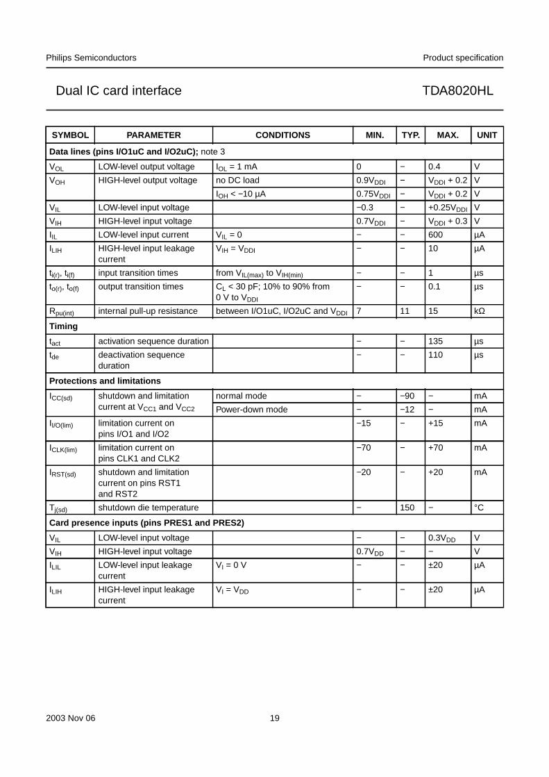
Data lines (pins I/O1 and I/O2); note 2
Vo(inactive) output voltage in inactivemode
no load 0 − 0.1 V
Iinactive = 1 mA − − 0.3 V
Io(inactive) current from pin I/O wheninactive
pin grounded − − −1 mA
VOL LOW-level output voltage IOL = 1 mA 0 − 0.3 V
VOH HIGH-level output voltage no DC load 0.9VCC − VCC + 0.1 V
IOH < −20 µA 0.8VCC − VCC + 0.1 V
IOH < −40 µA 0.75VCC − VCC + 0.1 V
Iedge current from pins I/O1and I/O2 when active pull-up
VOH = 0.9 VCC; CL = 30 pF −1 − − mA
td(edge) delay between falling edgeon pins I/O1, I/O2 and widthof active pull-up pulse
− 500 650 ns
VIL LOW-level input voltage −0.3 − +0.8 V
VIH HIGH-level input voltage 1.5 − VCC V
IIL LOW-level input current onpin I/O
VIL = 0; VCC = 5 V − − 600 µA
VIL = 0; VCC = 3 V − − 500 µA
ILIH HIGH-level input leakagecurrent on pin I/O
VIH = VCC − − 10 µA
ti(r), ti(f) input transition times from VIL(max) to VIH(min) − − 1.5 µs
to(r), to(f) output transition times CL < 30 pF; no DC load;10% to 90% from 0 V toVCC1 and VCC2
− − 0.1 µs
Ci input capacitance onpins I/O1 and I/O2
− − 10 pF
Rpu(int) internal pull-up resistancebetween pin I/O and VCC
10 14 18 kΩ
fmax maximum frequency onpins I/O1 and I/O2
− − 500 kHz
SYMBOL PARAMETER CONDITIONS MIN. TYP. MAX. UNIT
2003 Nov 06 19
Philips Semiconductors Product specification
Dual IC card interface TDA8020HL
Data lines (pins I/O1uC and I/O2uC); note 3
VOL LOW-level output voltage IOL = 1 mA 0 − 0.4 V
VOH HIGH-level output voltage no DC load 0.9VDDI − VDDI + 0.2 V
IOH < −10 µA 0.75VDDI − VDDI + 0.2 V
VIL LOW-level input voltage −0.3 − +0.25VDDI V
VIH HIGH-level input voltage 0.7VDDI − VDDI + 0.3 V
IIL LOW-level input current VIL = 0 − − 600 µA
ILIH HIGH-level input leakagecurrent
VIH = VDDI − − 10 µA
ti(r), ti(f) input transition times from VIL(max) to VIH(min) − − 1 µs
to(r), to(f) output transition times CL < 30 pF; 10% to 90% from0 V to VDDI
− − 0.1 µs
Rpu(int) internal pull-up resistance between I/O1uC, I/O2uC and VDDI 7 11 15 kΩ
Timing
tact activation sequence duration − − 135 µs
tde deactivation sequenceduration
− − 110 µs
Protections and limitations
ICC(sd) shutdown and limitationcurrent at VCC1 and VCC2
normal mode − −90 − mA
Power-down mode − −12 − mA
II/O(lim) limitation current onpins I/O1 and I/O2
−15 − +15 mA
ICLK(lim) limitation current onpins CLK1 and CLK2
−70 − +70 mA
IRST(sd) shutdown and limitationcurrent on pins RST1and RST2
−20 − +20 mA
Tj(sd) shutdown die temperature − 150 − °C
Card presence inputs (pins PRES1 and PRES2)
VIL LOW-level input voltage − − 0.3VDD V
VIH HIGH-level input voltage 0.7VDD − − V
ILIL LOW-level input leakagecurrent
VI = 0 V − − ±20 µA
ILIH HIGH-level input leakagecurrent
VI = VDD − − ±20 µA
SYMBOL PARAMETER CONDITIONS MIN. TYP. MAX. UNIT
2003 Nov 06 20
Philips Semiconductors Product specification
Dual IC card interface TDA8020HL
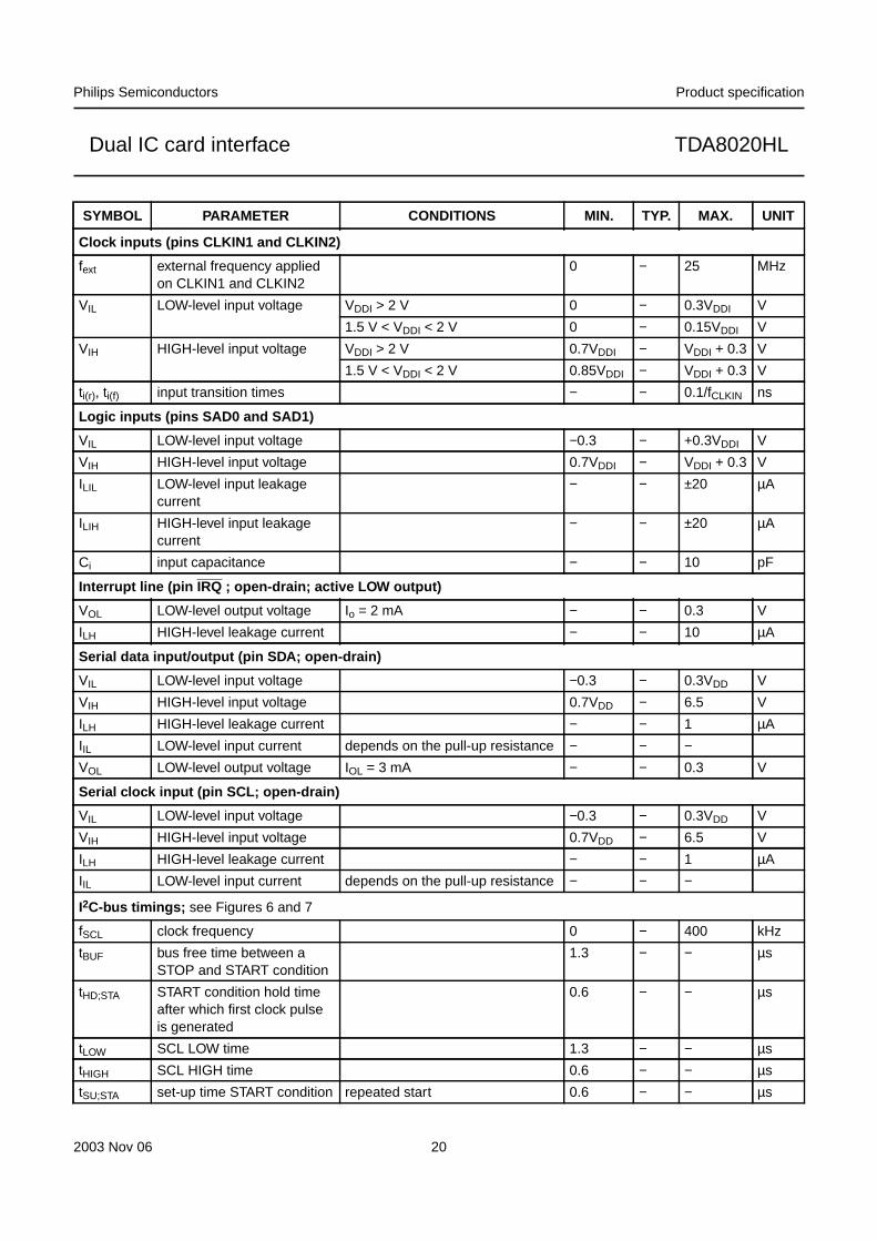
Clock inputs (pins CLKIN1 and CLKIN2)
fext external frequency appliedon CLKIN1 and CLKIN2
0 − 25 MHz
VIL LOW-level input voltage VDDI > 2 V 0 − 0.3VDDI V
1.5 V < VDDI < 2 V 0 − 0.15VDDI V
VIH HIGH-level input voltage VDDI > 2 V 0.7VDDI − VDDI + 0.3 V
1.5 V < VDDI < 2 V 0.85VDDI − VDDI + 0.3 V
ti(r), ti(f) input transition times − − 0.1/fCLKIN ns
Logic inputs (pins SAD0 and SAD1)
VIL LOW-level input voltage −0.3 − +0.3VDDI V
VIH HIGH-level input voltage 0.7VDDI − VDDI + 0.3 V
ILIL LOW-level input leakagecurrent
− − ±20 µA
ILIH HIGH-level input leakagecurrent
− − ±20 µA
Ci input capacitance − − 10 pF
Interrupt line (pin IRQ ; open-drain; active LOW output)
VOL LOW-level output voltage Io = 2 mA − − 0.3 V
ILH HIGH-level leakage current − − 10 µA
Serial data input/output (pin SDA; open-drain)
VIL LOW-level input voltage −0.3 − 0.3VDD V
VIH HIGH-level input voltage 0.7VDD − 6.5 V
ILH HIGH-level leakage current − − 1 µA
IIL LOW-level input current depends on the pull-up resistance − − −VOL LOW-level output voltage IOL = 3 mA − − 0.3 V
Serial clock input (pin SCL; open-drain)
VIL LOW-level input voltage −0.3 − 0.3VDD V
VIH HIGH-level input voltage 0.7VDD − 6.5 V
ILH HIGH-level leakage current − − 1 µA
IIL LOW-level input current depends on the pull-up resistance − − −
I2C-bus timings; see Figures 6 and 7
fSCL clock frequency 0 − 400 kHz
tBUF bus free time between aSTOP and START condition
1.3 − − µs
tHD;STA START condition hold timeafter which first clock pulseis generated
0.6 − − µs
tLOW SCL LOW time 1.3 − − µs
tHIGH SCL HIGH time 0.6 − − µs
tSU;STA set-up time START condition repeated start 0.6 − − µs
SYMBOL PARAMETER CONDITIONS MIN. TYP. MAX. UNIT

2003 Nov 06 21
Philips Semiconductors Product specification
Dual IC card interface TDA8020HL
Notes
1. Two ceramic multilayer capacitors of minimum 100 nF with low ESR should be used in order to meet thesespecifications.
2. Pin I/O1 has an internal 14 kΩ pull-up resistor to VCC1 and pin I/O2 has an internal 14 kΩ pull-up resistor to VCC2.
3. Pins I/O1uC and I/O2uC have an internal 11 kΩ pull-up resistor to VDDI.
4. The hold time required (not greater than 300 ns) to bridge the undefined region of the falling edge of SCL must beinternally provided by a transmitter.
tHD;DAT data hold time note 4 0 − − ns
tSU;DAT data set-up time 100 − − ns
tr rise time SDA and SCL − − 300 ns
tf fall time SDA and SCL − − 300 ns
tSU;STO set-up time STOP condition 0.6 − − µs
SYMBOL PARAMETER CONDITIONS MIN. TYP. MAX. UNIT
handbook, full pagewidth
MBC622
SDA
SCLP
STOP condition
SDA
SCLS
START condition
Fig.6 START and STOP conditions.
handbook, full pagewidth
SDA
MGA728
SDA
SCL
tSU;STA t SU;STO
tHD;STA
t BUF t LOW
t HD;DAT t HIGHt r
t f
t SU;DAT
Fig.7 I2C-bus timing waveforms.

2003N
ov06
22
Philips S
emiconductors
Product specification
Dual IC
card interfaceT
DA
8020HL
This text is here in white to force landscape pages to be rotated correctly when browsing through the pdf in the Acrobat reader.This text is here in_white to force landscape pages to be rotated correctly when browsing through the pdf in the Acrobat reader.This text is here inThis text is here inwhite to force landscape pages to be rotated correctly when browsing through the pdf in the Acrobat reader. white to force landscape pages to be ...
AP
PLIC
ATIO
N IN
FO
RM
ATIO
N
handbook, full pagewidth
220 Ω
1.5 to6.5 kΩ1 kΩ
MIC
RO
CO
NT
RO
LLE
R
100 kΩ
100 kΩ
0 kΩ
100nF
CARD_READ_LM01
CARD 2
3.3 V
1.5 V1.5 V 3.3 V to 6.5 V
1.5 V
3.3 V 3.3 V
10 µF(16 V)
10 µF
100 nF
10 µF(16 V)
100 nF
33 µF(16 V)
100 nF
220 nF
22 nF
220nF
220 nF
10 pF
100 nF
100 nF
33 pF
14.745 MHz
33 pF
1
2
3
4
5
6
7
8
9
10
11
12
13
14
15
16
17
18
19
20
40
39
38
37
36
35
34
33
32
31
30
29
28
27
26
25
24
23
22
21
P0_0
VCC
P0_1
P0_2
P0_3
P0_4
P0_5
P0_6
P0_7
EA
ALE
PSEN
P2_7
P2_6
P2_5
P2_4
P2_3
P2_2
P2_1
P2_0
P1_0
P1_1
P1_2
P1_3
P1_4
P1_5
P1_6
P1_7
RST
P3_0
P3_1
P3_2
P3_3
P3_4
P3_5
P3_6
P3_7
XTAL2
XTAL1VSS
C4C3C2C1C5IC6IC7IC8I
C8C7C6C5
C1IC2IC3IC4I
K1K2
TDA8020HL
FCE838
1
2
3
4
5
6
7
8
9 10 11 12 13 14 15 16
32 31 30 29 28 27 26 2524
23
22
21
20
19
18
17
PRES1
CGND1
CLK1
VCC1
RST1
I/O2
PRES2
CGND2
SAD1
CLK
2
VC
C2
RS
T2
GN
D
VU
P
SA
P
SB
P
VD
DA
SAD0
SDA
SCL
VDD
SAM
AGND
SBM
IRQ
CLK
IN1
I/O
1uC
I/O
2uC
CLK
IN2
CD
EL
VD
DI
I/O
1
100 kΩ
0 kΩ
100nF
CARD_READ_LM01
CARD 1
3.3 V
C4C3C2C1C5IC6IC7IC8I
C8C7C6C5
C1IC2IC3IC4I
K1K2
Fig.8 Application diagram.

2003 Nov 06 23
Philips Semiconductors Product specification
Dual IC card interface TDA8020HL
PACKAGE OUTLINE
UNITA
max. A1 A2 A3 bp c E(1) e HE L L p Zywv θ
REFERENCESOUTLINEVERSION
EUROPEANPROJECTION ISSUE DATE
IEC JEDEC JEITA
mm 1.60.200.05
1.451.35 0.25
0.40.3
0.180.12
7.16.9 0.8
9.158.85
0.90.5
70
o
o0.25 0.11 0.2
DIMENSIONS (mm are the original dimensions)
Note
1. Plastic or metal protrusions of 0.25 mm maximum per side are not included.
0.750.45
SOT358 -1 136E03 MS-02600-01-1903-02-25
D(1) (1)(1)
7.16.9
HD
9.158.85
EZ
0.90.5
D
bp
e
θ
EA1
A
Lp
detail X
L
(A )3
B
8
c
DH
bp
EH A2
v M B
D
ZD
A
ZE
e
v M A
X
1
32
25
24 17
16
9
y
pin 1 index
w M
w M
0 2.5 5 mm
scale
LQFP32: plastic low profile quad flat package; 32 leads; body 7 x 7 x 1.4 mm SOT358-1

2003 Nov 06 24
Philips Semiconductors Product specification
Dual IC card interface TDA8020HL
SOLDERING
Introduction to soldering surface mount packages
This text gives a very brief insight to a complex technology.A more in-depth account of soldering ICs can be found inour “Data Handbook IC26; Integrated Circuit Packages”(document order number 9398 652 90011).
There is no soldering method that is ideal for all surfacemount IC packages. Wave soldering can still be used forcertain surface mount ICs, but it is not suitable for fine pitchSMDs. In these situations reflow soldering isrecommended.
Reflow soldering
Reflow soldering requires solder paste (a suspension offine solder particles, flux and binding agent) to be appliedto the printed-circuit board by screen printing, stencilling orpressure-syringe dispensing before package placement.Driven by legislation and environmental forces theworldwide use of lead-free solder pastes is increasing.
Several methods exist for reflowing; for example,convection or convection/infrared heating in a conveyortype oven. Throughput times (preheating, soldering andcooling) vary between 100 and 200 seconds dependingon heating method.
Typical reflow peak temperatures range from215 to 270 °C depending on solder paste material. Thetop-surface temperature of the packages shouldpreferably be kept:
• below 225 °C (SnPb process) or below 245 °C (Pb-freeprocess)
– for all BGA, HTSSON-T and SSOP-T packages
– for packages with a thickness ≥ 2.5 mm
– for packages with a thickness < 2.5 mm and avolume ≥ 350 mm3 so called thick/large packages.
• below 240 °C (SnPb process) or below 260 °C (Pb-freeprocess) for packages with a thickness < 2.5 mm and avolume < 350 mm3 so called small/thin packages.
Moisture sensitivity precautions, as indicated on packing,must be respected at all times.
Wave soldering
Conventional single wave soldering is not recommendedfor surface mount devices (SMDs) or printed-circuit boardswith a high component density, as solder bridging andnon-wetting can present major problems.
To overcome these problems the double-wave solderingmethod was specifically developed.
If wave soldering is used the following conditions must beobserved for optimal results:
• Use a double-wave soldering method comprising aturbulent wave with high upward pressure followed by asmooth laminar wave.
• For packages with leads on two sides and a pitch (e):
– larger than or equal to 1.27 mm, the footprintlongitudinal axis is preferred to be parallel to thetransport direction of the printed-circuit board;
– smaller than 1.27 mm, the footprint longitudinal axismust be parallel to the transport direction of theprinted-circuit board.
The footprint must incorporate solder thieves at thedownstream end.
• For packages with leads on four sides, the footprint mustbe placed at a 45° angle to the transport direction of theprinted-circuit board. The footprint must incorporatesolder thieves downstream and at the side corners.
During placement and before soldering, the package mustbe fixed with a droplet of adhesive. The adhesive can beapplied by screen printing, pin transfer or syringedispensing. The package can be soldered after theadhesive is cured.
Typical dwell time of the leads in the wave ranges from3 to 4 seconds at 250 °C or 265 °C, depending on soldermaterial applied, SnPb or Pb-free respectively.
A mildly-activated flux will eliminate the need for removalof corrosive residues in most applications.
Manual soldering
Fix the component by first soldering twodiagonally-opposite end leads. Use a low voltage (24 V orless) soldering iron applied to the flat part of the lead.Contact time must be limited to 10 seconds at up to300 °C.
When using a dedicated tool, all other leads can besoldered in one operation within 2 to 5 seconds between270 and 320 °C.

2003 Nov 06 25
Philips Semiconductors Product specification
Dual IC card interface TDA8020HL
Suitability of surface mount IC packages for wave and reflow soldering methods
Notes
1. For more detailed information on the BGA packages refer to the “(LF)BGA Application Note” (AN01026); order a copyfrom your Philips Semiconductors sales office.
2. All surface mount (SMD) packages are moisture sensitive. Depending upon the moisture content, the maximumtemperature (with respect to time) and body size of the package, there is a risk that internal or external packagecracks may occur due to vaporization of the moisture in them (the so called popcorn effect). For details, refer to theDrypack information in the “Data Handbook IC26; Integrated Circuit Packages; Section: Packing Methods”.
3. These transparent plastic packages are extremely sensitive to reflow soldering conditions and must on no accountbe processed through more than one soldering cycle or subjected to infrared reflow soldering with peak temperatureexceeding 217 °C ± 10 °C measured in the atmosphere of the reflow oven. The package body peak temperaturemust be kept as low as possible.
4. These packages are not suitable for wave soldering. On versions with the heatsink on the bottom side, the soldercannot penetrate between the printed-circuit board and the heatsink. On versions with the heatsink on the top side,the solder might be deposited on the heatsink surface.
5. If wave soldering is considered, then the package must be placed at a 45° angle to the solder wave direction.The package footprint must incorporate solder thieves downstream and at the side corners.
6. Wave soldering is suitable for LQFP, TQFP and QFP packages with a pitch (e) larger than 0.8 mm; it is definitely notsuitable for packages with a pitch (e) equal to or smaller than 0.65 mm.
7. Wave soldering is suitable for SSOP, TSSOP, VSO and VSSOP packages with a pitch (e) equal to or larger than0.65 mm; it is definitely not suitable for packages with a pitch (e) equal to or smaller than 0.5 mm.
8. Hot bar or manual soldering is suitable for PMFP packages.
PACKAGE (1)SOLDERING METHOD
WAVE REFLOW (2)
BGA, HTSSON-T(3), LBGA, LFBGA, SQFP, SSOP-T(3), TFBGA,USON, VFBGA
not suitable suitable
DHVQFN, HBCC, HBGA, HLQFP, HSO, HSOP, HSQFP, HSSON,HTQFP, HTSSOP, HVQFN, HVSON, SMS
not suitable(4) suitable
PLCC(5), SO, SOJ suitable suitable
LQFP, QFP, TQFP not recommended(5)(6) suitable
SSOP, TSSOP, VSO, VSSOP not recommended(7) suitable
PMFP(8) not suitable not suitable

2003 Nov 06 26
Philips Semiconductors Product specification
Dual IC card interface TDA8020HL
DATA SHEET STATUS
Notes
1. Please consult the most recently issued data sheet before initiating or completing a design.
2. The product status of the device(s) described in this data sheet may have changed since this data sheet waspublished. The latest information is available on the Internet at URL http://www.semiconductors.philips.com.
3. For data sheets describing multiple type numbers, the highest-level product status determines the data sheet status.
LEVELDATA SHEET
STATUS(1)PRODUCT
STATUS(2)(3) DEFINITION
I Objective data Development This data sheet contains data from the objective specification for productdevelopment. Philips Semiconductors reserves the right to change thespecification in any manner without notice.
II Preliminary data Qualification This data sheet contains data from the preliminary specification.Supplementary data will be published at a later date. PhilipsSemiconductors reserves the right to change the specification withoutnotice, in order to improve the design and supply the best possibleproduct.
III Product data Production This data sheet contains data from the product specification. PhilipsSemiconductors reserves the right to make changes at any time in orderto improve the design, manufacturing and supply. Relevant changes willbe communicated via a Customer Product/Process Change Notification(CPCN).
DEFINITIONS
Short-form specification The data in a short-formspecification is extracted from a full data sheet with thesame type number and title. For detailed information seethe relevant data sheet or data handbook.
Limiting values definition Limiting values given are inaccordance with the Absolute Maximum Rating System(IEC 60134). Stress above one or more of the limitingvalues may cause permanent damage to the device.These are stress ratings only and operation of the deviceat these or at any other conditions above those given in theCharacteristics sections of the specification is not implied.Exposure to limiting values for extended periods mayaffect device reliability.
Application information Applications that aredescribed herein for any of these products are forillustrative purposes only. Philips Semiconductors makeno representation or warranty that such applications will besuitable for the specified use without further testing ormodification.
DISCLAIMERS
Life support applications These products are notdesigned for use in life support appliances, devices, orsystems where malfunction of these products canreasonably be expected to result in personal injury. PhilipsSemiconductors customers using or selling these productsfor use in such applications do so at their own risk andagree to fully indemnify Philips Semiconductors for anydamages resulting from such application.
Right to make changes Philips Semiconductorsreserves the right to make changes in the products -including circuits, standard cells, and/or software -described or contained herein in order to improve designand/or performance. When the product is in full production(status ‘Production’), relevant changes will becommunicated via a Customer Product/Process ChangeNotification (CPCN). Philips Semiconductors assumes noresponsibility or liability for the use of any of theseproducts, conveys no licence or title under any patent,copyright, or mask work right to these products, andmakes no representations or warranties that theseproducts are free from patent, copyright, or mask workright infringement, unless otherwise specified.
2003 Nov 06 27
Philips Semiconductors Product specification
Dual IC card interface TDA8020HL
PURCHASE OF PHILIPS I2C COMPONENTS
Purchase of Philips I2C components conveys a license under the Philips’ I2C patent to use thecomponents in the I2C system provided the system conforms to the I2C specification defined byPhilips. This specification can be ordered using the code 9398 393 40011.

© Koninklijke Philips Electronics N.V. 2003 SCA75All rights are reserved. Reproduction in whole or in part is prohibited without the prior written consent of the copyright owner.
The information presented in this document does not form part of any quotation or contract, is believed to be accurate and reliable and may be changedwithout notice. No liability will be accepted by the publisher for any consequence of its use. Publication thereof does not convey nor imply any licenseunder patent- or other industrial or intellectual property rights.
Philips Semiconductors – a worldwide company
Contact information
For additional information please visit http://www.semiconductors.philips.com . Fax: +31 40 27 24825For sales offices addresses send e-mail to: [email protected] .
Printed in The Netherlands 753504/03/pp28 Date of release: 2003 Nov 06 Document order number: 9397 750 11554