Embed Size (px)
Citation preview
Minimum PCB Footprint Point-of-Load DC-DC Converter Realized with Switched-Capacitor Architecture
Vincent W Ng, Michael D Seeman, Seth R Sanders
University of California, Berkeley 550 Cory Hall,
Berkeley, CA 94703, USA vwng, mseeman, [email protected]
Abstract -- This work reports on the design and test of a CMOS-based Switched Capacitor (SC) DC-DC conversion integrated circuit (IC) for the point-of-load (POL) application conventionally addressed with the buck converter. A 12V-to-1.5V converter is fabricated in a 0.18µm technology, with an active die area of 3mm2. There is a significant reduction in printed circuit board (PCB) footprint, passive component height and cost when compared to surveyed buck converters. The converter achieves 93% peak efficiency and an efficiency of 80% over an output current range of 7mA to 1A. This work demonstrates the vast potential of SC converters for wide-range voltage conversion in deep-submicron CMOS technologies, when cost and efficiency are of critical importance. Index Terms – DC-DC power conversion, switched-capacitor circuits, integrated power converter
I. INTRODUCTION This paper reports on the design and test of a 12V-to-
1.5V Switched-Capacitor (SC) DC-DC converter in a 0.18 µm CMOS technology for the point-of-load (POL) application conventionally addressed with the inductor-based buck converter. The buck converter requires at least one substantial inductor, which takes up a significant proportion of the overall printed-circuit-board (PCB) area that the converter occupies. As shown later in Section VII (Table IV), by using an SC DC-DC converter, this inductor is replaced by a few, but much smaller power-train capacitors, resulting in a much reduced PCB area and also much reduced component cost.
The advantages of SC DC-DC conversion technology
can be motivated at a theoretical level, as will be done here briefly (see [1, 11] for greater depth), before continuing with the practical results demonstrated in this work. The power switches in the buck converter each block the full input voltage and support the full
output current. For a large or even moderate conversion ratio, this leads to a high switch total Volt-Ampere product (∑VA), and causes the buck converter to suffer from low efficiency or poor power device utilization when used in such an application [1]. However, in contrast, the switches in a ladder or Dickson SC converter only block a fraction of the input voltage, while supporting a fraction of the output current [1]. This not only enables utilization of native low-voltage CMOS transistors in a modern low-cost CMOS process, but also leads to a low switch ∑VA, and allows the SC converters to sustain high efficiency with a high conversion ratio [1]. Moreover, SC converters can also sustain high efficiency over a very wide load range without requiring additional special modes, in contrast to, for example the Pulse Frequency Modulation (PFM) used in many inductor-based converters. Switched Capacitor converter efficiency can be improved at low-load condition simply by reducing the switching frequency.
Most SC converters that are commercially available
and/or are discussed in recent literature are used in low-conversion-ratio applications while high-conversion-ratio applications are dominated by the buck converter. Further, IC based SC converters have been mainly relegated to sub 1 W applications in existing commercial products. On the other hand, we note that the industry has developed highly functional MOS power devices that have allowed the continued success of the buck converter in high-conversion-ratio applications with power levels well beyond 1 W. This paper discusses circuit designs that allow SC converters to operate efficiently in high-conversion-ratio applications, while delivering 1 W and more, and to be more than competitive with the buck converter.
II. ARCHITECTURE Fig. 1 shows the schematic of the 8-to-1 Dickson
converter implemented in this work. In contrast to the original work of Dickson implementing a voltage
1575978-1-4244-2893-9/09/$25.00 ©2009 IEEE
Authorized licensed use limited to: Univ of Calif Berkeley. Downloaded on February 10, 2010 at 23:22 from IEEE Xplore. Restrictions apply.
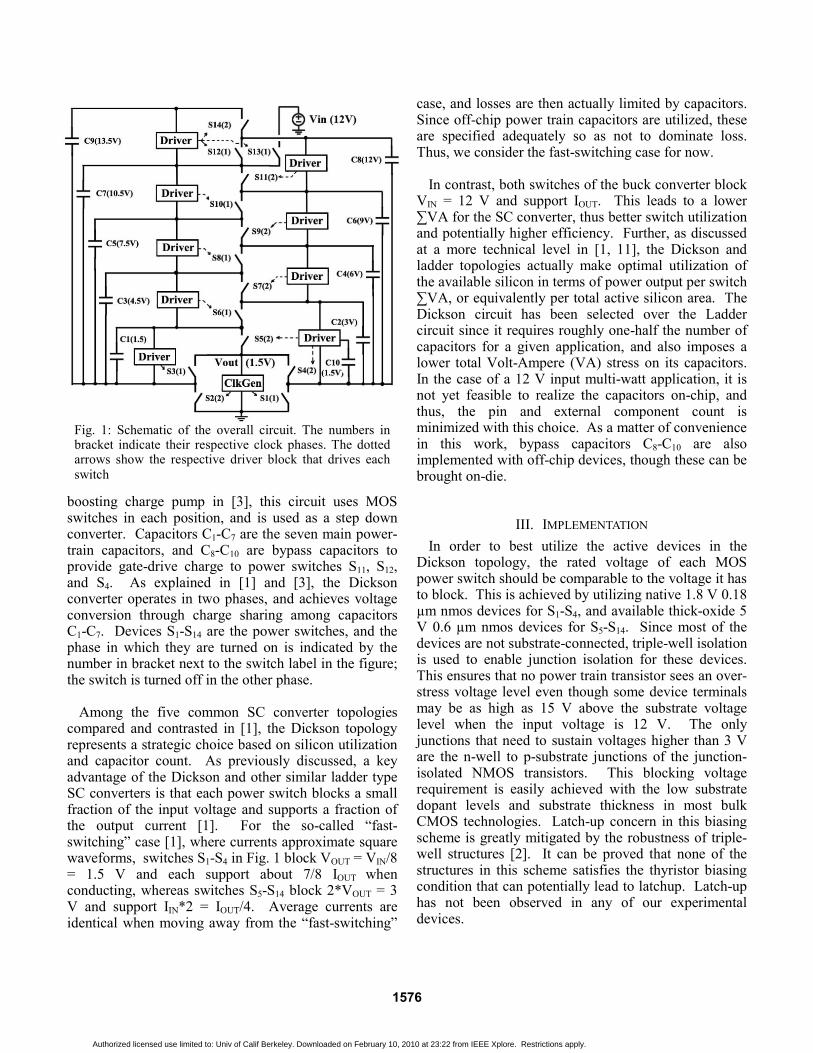
boosting charge pump in [3], this circuit uses MOS switches in each position, and is used as a step down converter. Capacitors C1-C7 are the seven main power-train capacitors, and C8-C10 are bypass capacitors to provide gate-drive charge to power switches S11, S12, and S4. As explained in [1] and [3], the Dickson converter operates in two phases, and achieves voltage conversion through charge sharing among capacitors C1-C7. Devices S1-S14 are the power switches, and the phase in which they are turned on is indicated by the number in bracket next to the switch label in the figure; the switch is turned off in the other phase.
Among the five common SC converter topologies
compared and contrasted in [1], the Dickson topology represents a strategic choice based on silicon utilization and capacitor count. As previously discussed, a key advantage of the Dickson and other similar ladder type SC converters is that each power switch blocks a small fraction of the input voltage and supports a fraction of the output current [1]. For the so-called “fast-switching” case [1], where currents approximate square waveforms, switches S1-S4 in Fig. 1 block VOUT = VIN/8 = 1.5 V and each support about 7/8 IOUT when conducting, whereas switches S5-S14 block 2*VOUT = 3 V and support IIN*2 = IOUT/4. Average currents are identical when moving away from the “fast-switching”
case, and losses are then actually limited by capacitors. Since off-chip power train capacitors are utilized, these are specified adequately so as not to dominate loss. Thus, we consider the fast-switching case for now.
In contrast, both switches of the buck converter block
VIN = 12 V and support IOUT. This leads to a lower ∑VA for the SC converter, thus better switch utilization and potentially higher efficiency. Further, as discussed at a more technical level in [1, 11], the Dickson and ladder topologies actually make optimal utilization of the available silicon in terms of power output per switch ∑VA, or equivalently per total active silicon area. The Dickson circuit has been selected over the Ladder circuit since it requires roughly one-half the number of capacitors for a given application, and also imposes a lower total Volt-Ampere (VA) stress on its capacitors. In the case of a 12 V input multi-watt application, it is not yet feasible to realize the capacitors on-chip, and thus, the pin and external component count is minimized with this choice. As a matter of convenience in this work, bypass capacitors C8-C10 are also implemented with off-chip devices, though these can be brought on-die.
III. IMPLEMENTATION In order to best utilize the active devices in the
Dickson topology, the rated voltage of each MOS power switch should be comparable to the voltage it has to block. This is achieved by utilizing native 1.8 V 0.18 µm nmos devices for S1-S4, and available thick-oxide 5 V 0.6 µm nmos devices for S5-S14. Since most of the devices are not substrate-connected, triple-well isolation is used to enable junction isolation for these devices. This ensures that no power train transistor sees an over-stress voltage level even though some device terminals may be as high as 15 V above the substrate voltage level when the input voltage is 12 V. The only junctions that need to sustain voltages higher than 3 V are the n-well to p-substrate junctions of the junction-isolated NMOS transistors. This blocking voltage requirement is easily achieved with the low substrate dopant levels and substrate thickness in most bulk CMOS technologies. Latch-up concern in this biasing scheme is greatly mitigated by the robustness of triple-well structures [2]. It can be proved that none of the structures in this scheme satisfies the thyristor biasing condition that can potentially lead to latchup. Latch-up has not been observed in any of our experimental devices.
Fig. 1: Schematic of the overall circuit. The numbers in bracket indicate their respective clock phases. The dotted arrows show the respective driver block that drives each switch
1576
Authorized licensed use limited to: Univ of Calif Berkeley. Downloaded on February 10, 2010 at 23:22 from IEEE Xplore. Restrictions apply.
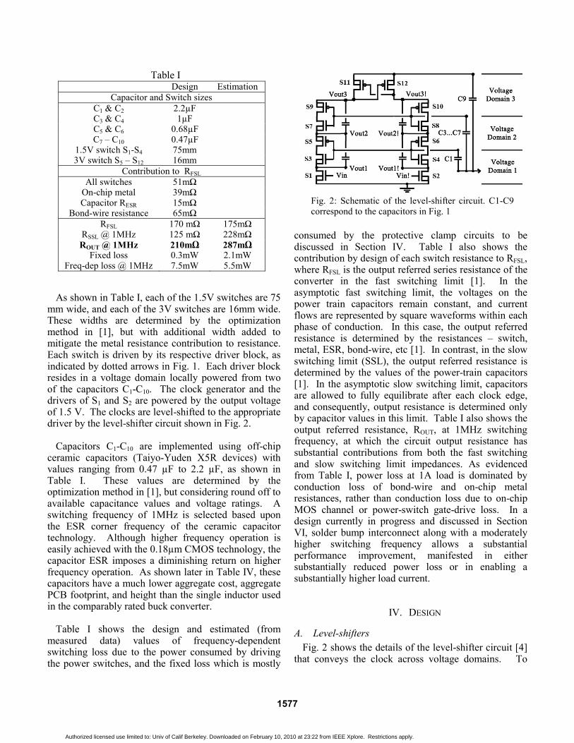
As shown in Table I, each of the 1.5V switches are 75
mm wide, and each of the 3V switches are 16mm wide. These widths are determined by the optimization method in [1], but with additional width added to mitigate the metal resistance contribution to resistance. Each switch is driven by its respective driver block, as indicated by dotted arrows in Fig. 1. Each driver block resides in a voltage domain locally powered from two of the capacitors C1-C10. The clock generator and the drivers of S1 and S2 are powered by the output voltage of 1.5 V. The clocks are level-shifted to the appropriate driver by the level-shifter circuit shown in Fig. 2.
Capacitors C1-C10 are implemented using off-chip
ceramic capacitors (Taiyo-Yuden X5R devices) with values ranging from 0.47 µF to 2.2 µF, as shown in Table I. These values are determined by the optimization method in [1], but considering round off to available capacitance values and voltage ratings. A switching frequency of 1MHz is selected based upon the ESR corner frequency of the ceramic capacitor technology. Although higher frequency operation is easily achieved with the 0.18µm CMOS technology, the capacitor ESR imposes a diminishing return on higher frequency operation. As shown later in Table IV, these capacitors have a much lower aggregate cost, aggregate PCB footprint, and height than the single inductor used in the comparably rated buck converter.
Table I shows the design and estimated (from
measured data) values of frequency-dependent switching loss due to the power consumed by driving the power switches, and the fixed loss which is mostly
consumed by the protective clamp circuits to be discussed in Section IV. Table I also shows the contribution by design of each switch resistance to RFSL, where RFSL is the output referred series resistance of the converter in the fast switching limit [1]. In the asymptotic fast switching limit, the voltages on the power train capacitors remain constant, and current flows are represented by square waveforms within each phase of conduction. In this case, the output referred resistance is determined by the resistances – switch, metal, ESR, bond-wire, etc [1]. In contrast, in the slow switching limit (SSL), the output referred resistance is determined by the values of the power-train capacitors [1]. In the asymptotic slow switching limit, capacitors are allowed to fully equilibrate after each clock edge, and consequently, output resistance is determined only by capacitor values in this limit. Table I also shows the output referred resistance, ROUT, at 1MHz switching frequency, at which the circuit output resistance has substantial contributions from both the fast switching and slow switching limit impedances. As evidenced from Table I, power loss at 1A load is dominated by conduction loss of bond-wire and on-chip metal resistances, rather than conduction loss due to on-chip MOS channel or power-switch gate-drive loss. In a design currently in progress and discussed in Section VI, solder bump interconnect along with a moderately higher switching frequency allows a substantial performance improvement, manifested in either substantially reduced power loss or in enabling a substantially higher load current.
IV. DESIGN
A. Level-shifters Fig. 2 shows the details of the level-shifter circuit [4]
that conveys the clock across voltage domains. To
Fig. 2: Schematic of the level-shifter circuit. C1-C9 correspond to the capacitors in Fig. 1
Table I Design Estimation Capacitor and Switch sizes
C1 & C2 2.2µF C3 & C4 1µF C5 & C6 0.68µF C7 – C10 0.47µF
1.5V switch S1-S4 75mm 3V switch S5 – S12 16mm
Contribution to RFSL All switches 51mΩ
On-chip metal 39mΩ Capacitor RESR 15mΩ
Bond-wire resistance 65mΩ RFSL 170 mΩ 175mΩ
RSSL @ 1MHz 125 mΩ 228mΩROUT @ 1MHz 210mΩ 287mΩ
Fixed loss 0.3mW 2.1mWFreq-dep loss @ 1MHz 7.5mW 5.5mW
1577
Authorized licensed use limited to: Univ of Calif Berkeley. Downloaded on February 10, 2010 at 23:22 from IEEE Xplore. Restrictions apply.
obtain more voltage domains, as used in the power train of Fig. 1, Voltage domain 2 is instantiated multiple times depending on the number of voltage domains required, but is only shown once in the figure for simplicity. The circuit consists of two strings of transistors connected at the top by a cross-coupled half-latch. It operates with either switches S1 or S2 pulling down one string, and the cross-coupled pair S11 and S12 pulling up the other string. Switches S3-S10 act as cascode devices to limit the voltage swing at each node, such that each transistor is only subjected to a fraction of the overall voltage applied to these two strings of transistors.
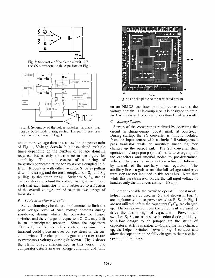
B. Protection clamp circuits Active clamping circuits are implemented to limit the
peak voltage level of each voltage domains during shutdown, during which the converter no longer switches and the voltages of capacitors C1-C10 may drift in an unanticipated manner. Since the capacitors effectively define the chip voltage domains, this transient could place an over-voltage stress on the on-chip devices. The clamp circuits guarantee no exposure to over-stress voltages during shutdown. Fig. 3 shows the clamp circuit implemented in this work. The comparator detects an over-voltage condition, and turns
on an NMOS transistor to drain current across the voltage domain. This clamp circuit is designed to drain 5mA when on and to consume less than 10µA when off.
C. Startup Scheme Startup of the converter is realized by operating the
circuit in charge-pump (boost) mode at power-up. During startup, the SC converter is initially isolated from the input source with a single full-voltage-rated pass transistor while an auxiliary linear regulator charges up the output rail. The SC converter then operates in charge-pump (boost) mode to charge up all the capacitors and internal nodes to pre-determined values. The pass transistor is then activated, followed by turn-off of the auxiliary linear regulator. The auxiliary linear regulator and the full-voltage-rated pass transistor are not included in this test chip. Note that while this pass transistor blocks the full input voltage, it handles only the input current IIN = 1/8 IOUT.
In order to enable the circuit to operate in boost mode,
helper transistors as used in [5], and shown in Fig. 4, are implemented since power switches S3-S14 in Fig. 1 are not utilized before the capacitors C1-C10 are charged up. Drivers powered from the output rail are used to drive the two strings of capacitors. Power train switches S3-S14 act as passive junction diodes, initially, to allow charge to be pumped up the string of capacitors. After capacitors C1-C10 are partially charged up, the helper switches shown in Fig. 4 conduct and allow the capacitors to be fully charged to their nominal open circuit voltages.
Fig. 3: Schematic of the clamp circuit. C7 and C9 correspond to the capacitors in Fig. 1
Fig. 4: Schematic of the helper switches (in black) that enable boost mode during startup. The part in gray is a portion of the circuit in Fig. 1.
Fig. 5: The die photo of the fabricated design.
1578
Authorized licensed use limited to: Univ of Calif Berkeley. Downloaded on February 10, 2010 at 23:22 from IEEE Xplore. Restrictions apply.
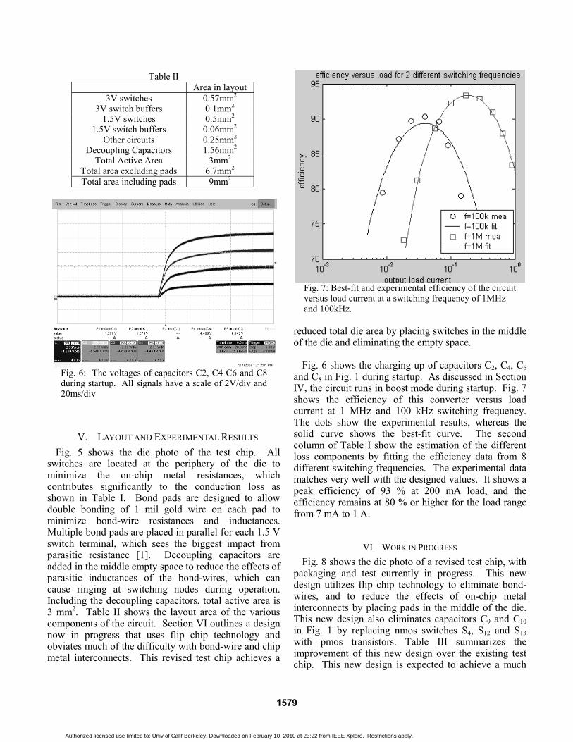
V. LAYOUT AND EXPERIMENTAL RESULTS Fig. 5 shows the die photo of the test chip. All
switches are located at the periphery of the die to minimize the on-chip metal resistances, which contributes significantly to the conduction loss as shown in Table I. Bond pads are designed to allow double bonding of 1 mil gold wire on each pad to minimize bond-wire resistances and inductances. Multiple bond pads are placed in parallel for each 1.5 V switch terminal, which sees the biggest impact from parasitic resistance [1]. Decoupling capacitors are added in the middle empty space to reduce the effects of parasitic inductances of the bond-wires, which can cause ringing at switching nodes during operation. Including the decoupling capacitors, total active area is 3 mm2. Table II shows the layout area of the various components of the circuit. Section VI outlines a design now in progress that uses flip chip technology and obviates much of the difficulty with bond-wire and chip metal interconnects. This revised test chip achieves a
reduced total die area by placing switches in the middle of the die and eliminating the empty space.
Fig. 6 shows the charging up of capacitors C2, C4, C6
and C8 in Fig. 1 during startup. As discussed in Section IV, the circuit runs in boost mode during startup. Fig. 7 shows the efficiency of this converter versus load current at 1 MHz and 100 kHz switching frequency. The dots show the experimental results, whereas the solid curve shows the best-fit curve. The second column of Table I show the estimation of the different loss components by fitting the efficiency data from 8 different switching frequencies. The experimental data matches very well with the designed values. It shows a peak efficiency of 93 % at 200 mA load, and the efficiency remains at 80 % or higher for the load range from 7 mA to 1 A.
VI. WORK IN PROGRESS Fig. 8 shows the die photo of a revised test chip, with
packaging and test currently in progress. This new design utilizes flip chip technology to eliminate bond-wires, and to reduce the effects of on-chip metal interconnects by placing pads in the middle of the die. This new design also eliminates capacitors C9 and C10 in Fig. 1 by replacing nmos switches S4, S12 and S13 with pmos transistors. Table III summarizes the improvement of this new design over the existing test chip. This new design is expected to achieve a much
Table II Area in layout
3V switches 0.57mm2
3V switch buffers 0.1mm2
1.5V switches 0.5mm2
1.5V switch buffers 0.06mm2
Other circuits 0.25mm2
Decoupling Capacitors 1.56mm2
Total Active Area 3mm2
Total area excluding pads 6.7mm2
Total area including pads 9mm2
Fig. 6: The voltages of capacitors C2, C4 C6 and C8 during startup. All signals have a scale of 2V/div and 20ms/div
Fig. 7: Best-fit and experimental efficiency of the circuit versus load current at a switching frequency of 1MHz and 100kHz.
1579
Authorized licensed use limited to: Univ of Calif Berkeley. Downloaded on February 10, 2010 at 23:22 from IEEE Xplore. Restrictions apply.
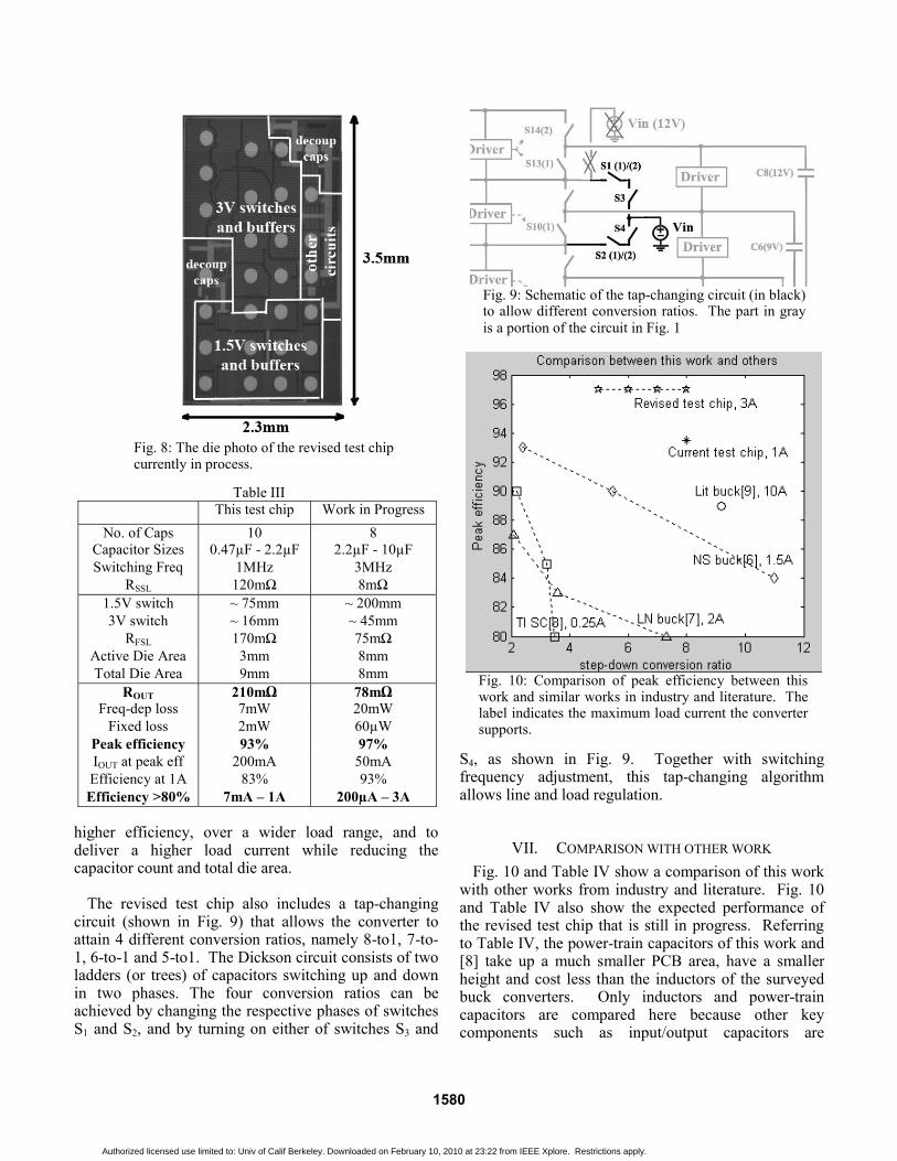
higher efficiency, over a wider load range, and to deliver a higher load current while reducing the capacitor count and total die area.
The revised test chip also includes a tap-changing
circuit (shown in Fig. 9) that allows the converter to attain 4 different conversion ratios, namely 8-to1, 7-to-1, 6-to-1 and 5-to1. The Dickson circuit consists of two ladders (or trees) of capacitors switching up and down in two phases. The four conversion ratios can be achieved by changing the respective phases of switches S1 and S2, and by turning on either of switches S3 and
S4, as shown in Fig. 9. Together with switching frequency adjustment, this tap-changing algorithm allows line and load regulation.
VII. COMPARISON WITH OTHER WORK Fig. 10 and Table IV show a comparison of this work
with other works from industry and literature. Fig. 10 and Table IV also show the expected performance of the revised test chip that is still in progress. Referring to Table IV, the power-train capacitors of this work and [8] take up a much smaller PCB area, have a smaller height and cost less than the inductors of the surveyed buck converters. Only inductors and power-train capacitors are compared here because other key components such as input/output capacitors are
Fig. 8: The die photo of the revised test chip currently in process.
Table III This test chip Work in Progress
No. of Caps 10 8Capacitor Sizes 0.47µF - 2.2µF 2.2µF - 10µFSwitching Freq 1MHz 3MHz
RSSL 120mΩ 8mΩ1.5V switch ~ 75mm ~ 200mm3V switch ~ 16mm ~ 45mm
RFSL 170mΩ 75mΩActive Die Area 3mm 8mmTotal Die Area 9mm 8mm
ROUT 210mΩ 78mΩFreq-dep loss 7mW 20mW
Fixed loss 2mW 60µWPeak efficiency 93% 97%IOUT at peak eff 200mA 50mAEfficiency at 1A 83% 93%Efficiency >80% 7mA – 1A 200µA – 3A
Fig. 9: Schematic of the tap-changing circuit (in black) to allow different conversion ratios. The part in gray is a portion of the circuit in Fig. 1
Fig. 10: Comparison of peak efficiency between this work and similar works in industry and literature. The label indicates the maximum load current the converter supports.
1580
Authorized licensed use limited to: Univ of Calif Berkeley. Downloaded on February 10, 2010 at 23:22 from IEEE Xplore. Restrictions apply.
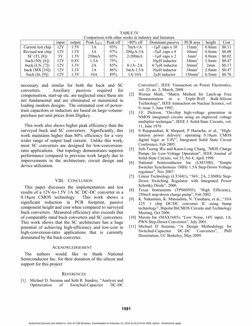
necessary and similar for both the buck and SC converters. Auxiliary passives required for compensation, start-up etc. are neglected since these are not fundamental and are eliminated or minimized in leading modern designs. The estimated cost of power-train capacitors or inductors are based on large-volume-purchase per-unit prices from Digikey.
This work also shows higher peak efficiency than the
surveyed buck and SC converters. Significantly, this work maintains higher than 80% efficiency for a very wider range of output load current. Unlike this work, most SC converters are designed for low-conversion-ratio applications. Our topology demonstrates superior performance compared to previous work largely due to improvements in the architecture, circuit design and device utilization.
VIII. CONCLUSION This paper discusses the implementation and test
results of a 12V-to-1.5V 1A SC DC-DC converter in a 0.18µm CMOS technology. This work shows a significant reduction in PCB footprint, passive component height and cost when compared to surveyed buck converters. Measured efficiency also exceeds that of comparably rated buck converters and SC converters. This work shows that the SC architecture has a huge potential of achieving high-efficiency and low-cost in high-conversion-ratio applications that is currently dominated by the buck converter.
ACKNOWLEDGEMENT The authors would like to thank National
Semiconductor Inc. for their donation of the silicon and support for this project
REFERENCES [1] Michael D. Seeman and Seth R. Sanders, “Analysis and
Optimization of Switched-Capacitor DC-DC
Converters”, IEEE Transaction on Power Electronics, vol. 23, no. 2, March, 2008
[2] Werner Muth, “Matrix Method for Latch-up Free Demonstration in a Triple-Well Bulk-Silicon Technology”, IEEE transaction on Nuclear Science, vol 9, issue 3, June 1992.
[3] J.F. Dickson, “On-chip high-voltage generation in NMOS integrated circuits using an improved voltage multiplier technique”, IEEE J. Solid-State Circuits, vol. 11, June 1976
[4] S Rajapandian, K Shepard, P Hazucha, et al., “High-tension power delivery: operating 0.18µm CMOS digital logic at 5.4V”, Integrated Solid State Circuit Conference, Feb 2005.
[5] Jieh-Tsorng Wu and Kuen-Long Chang, “MOS Charge Pumps for Low-Voltage Operation”, IEEE Journal of Solid-State Circuits, vol 33, No 4, April 1998.
[6] National Semiconductor Inc (LM3100), “Simple Switcher Synchronous 1MHz 1.5A Step-Down Voltage regulator”, Nov 2007.
[7] Linear Technology (LT3681), “36V, 2A, 2.8MHz Step-Down Switching Regulator with Integrated Power Schottky Diode”, 2006.
[8] Texas Instruments (TPS60503), “High Efficiency, 250mA step-down charge pump”, Feb 2002.
[9] K. Nakamura, K. Matsushita, N. Yasuhara, et al., “10A 12V 1 chip DC/DC converter IC using bump technology”, Bipolar/BiCMOS Circuits and Technology Meeting, Oct 2006.
[10] Maxim Inc (MAX1685), “Low Noise, 14V input, 1A, PWN Step-Down Converters”, July 2001.
[11] Michael D Seeman, “A Design Methodology for Switched-Capacitor DC-DC Converters”, PhD Dissertation, UC Berkeley, May 2009
TABLE IVComparison with other works in industry and literature
input output Peak IOUT Peak eff >80% eff Dominant passive PCB area height CostCurrent test chip 12V 1.5V 1A 93% 7mA-1A ~1µF caps x 10 13mm2 0.8mm $0.11Revised test chip 12V 1.5V 3A 97% 200µA-3A ~5µF caps x 8 10mm2 0.8mm $0.08
SC (TI, [8]) 5V 1.5V 250mA 85% 2-200mA ~1µF caps x 2 3mm2 0.8mm $0.02buck (NS, [6]) 12V 0.8V 1.5A 75% - 10µH inductor 34mm2 2.8mm $0.47buck (LN, [7]) 12V 3.3V 2A 85% 0.1A- 2A 4.7µH inductor 36mm2 2mm $0.17
buck (MX [10]) 12V 3.3V 1A 86% 3mA-1.5A 10µH inductor 34mm2 2.8mm $0.47buck (lit, [9]) 12V 1.3V 10A 89% 1A-10A 2µH inductor 156mm2 6.5mm $0.76
1581
Authorized licensed use limited to: Univ of Calif Berkeley. Downloaded on February 10, 2010 at 23:22 from IEEE Xplore. Restrictions apply.