Embed Size (px)
Citation preview

© KEMET Electronics Corporation • P.O. Box 5928 • Greenville, SC 29606 • 864-963-6300 • www.kemet.com C1013_X7R_FT-CAP_SMD • 5/4/2018 1One world. One KEMET
Overview
The KEMET Flexible Termination (FT-CAP) multilayer ceramic capacitor in X7R dielectric incorporates a unique, flexible termination system that is integrated with the KEMET standard termination materials. A conductive silver epoxy is utilized between the base metal and nickel barrier layers of KEMET’s standard termination system in order to establish pliability, while maintaining terminal strength, solderability and electrical performance. This technology was developed in order to address the primary failure mode of MLCCs – flex cracks, which are typically the result of excessive tensile and shear stresses produced during board flexure and thermal cycling. Flexible termination technology inhibits the transfer of board stress to the rigid ceramic body, therefore mitigating flex cracks which can result in low IR or short circuit failures. Although this technology does not eliminate the potential for mechanical damage that may propagate during extreme environmental and handling conditions, it does provide superior flex performance over standard termination systems. FT-CAP complements the KEMET Open Mode, Floating Electrode (FE-CAP), Floating Electrode with Flexible Termination (FF-CAP) and KEMET Power Solutions
(KPS) product lines by providing a complete portfolio of flex mitigation solutions. Combined with the stability of an X7R dielectric and designed to accommodate all capacitance requirements, these flex-robust devices are RoHS-compliant, offer up to 5 mm of flex-bend capability and exhibit a predictable change in capacitance with respect to time and voltage. Capacitance change with reference to ambient temperature is limited to ±15% from −55°C to +125°C. In addition to commercial grade, automotive grade devices are available which meet the demanding Automotive Electronics Council's AEC–Q200 qualification requirements.
Surface Mount Multilayer Ceramic Chip Capacitors (SMD MLCCs)
Flexible Termination System (FT-CAP), X7R Dielectric, 6.3 – 250 VDC (Commercial Grade)
Ordering Information
C 1206 X 106 K 4 R A C TU
CeramicCase Size (L" x W")
Specification/Series
Capacitance Code (pF)
Capacitance Tolerance
Rated Voltage (VDC)
DielectricFailure Rate/
DesignTermination Finish1 Packaging/Grade
(C-Spec)2
060308051206121018081812182522202225
X = Flexible termination
Two significant
digits + number of
zeros
J = ±5%K = ±10%M = ±20%
9 = 6.38 = 104 = 163 = 255 = 501 = 1002 = 200A = 250
R = X7R A = N/A C = 100% Matte SnL = SnPb (5% Pb minimum)
See "Packaging C-Spec
Ordering Options Table"
1 Additional termination finish options may be available. Contact KEMET for details.
© KEMET Electronics Corporation • P.O. Box 5928 • Greenville, SC 29606 • 864-963-6300 • www.kemet.com C1013_X7R_FT-CAP_SMD • 5/4/2018 2
Surface Mount Multilayer Ceramic Chip Capacitors (SMD MLCCs)Flexible Termination System (FT-CAP), X7R Dielectric, 6.3 – 250 VDC (Commercial Grade)
Packaging C-Spec Ordering Options Table
Packaging Type1 Packaging/Grade Ordering Code (C-Spec)
Bulk Bag/Unmarked Not required (Blank)7" Reel/Unmarked TU
13" Reel/Unmarked 7411 (EIA 0603 and smaller case sizes)7210 (EIA 0805 and larger case sizes)
7" Reel/Marked TM
13" Reel/Marked 7040 (EIA 0603 and smaller case sizes)7215 (EIA 0805 and larger case sizes)
7" Reel/Unmarked/2 mm pitch2 708113" Reel/Unmarked/2 mm pitch2 7082
1 Default packaging is "Bulk Bag." An ordering code C-Spec is not required for "Bulk Bag" packaging.1 The terms "Marked" and "Unmarked" pertain to laser marking option of capacitors. All packaging options labeled as "Unmarked" will contain
capacitors that have not been laser marked. Please contact KEMET if you require a laser marked option. For more information see "Capacitor Marking."2 The 2 mm pitch option allows for double the packaging quantity of capacitors on a given reel size. This option is limited to EIA 0603 (1608 metric) case
size devices. For more information regarding 2 mm pitch option see "Tape & Reel Packaging Information."
Benefits
• −55°C to +125°C operating temperature range• Superior flex performance (up to 5 mm)• High capacitance flex mitigation• Lead (Pb)-free, RoHS and REACH compliant • EIA 0603, 0805, 1206, 1210, 1808, 1812, 1825, 2220, and
2225 case sizes• DC voltage ratings of 6.3 V, 10 V, 16 V, 25 V, 50 V, 100 V,
200 V, and 250 V
• Capacitance offerings ranging from 180 pF to 22 μF• Available capacitance tolerances of ±5%, ±10%, and ±20%• Automotive (AEC-Q200) grade available• Non-polar device, minimizing installation concerns• 100% pure matte tin-plated termination finish allowing for
excellent solderability• SnPb termination finish option available upon request
(5% Pb minimum)
Applications
Typical applications include circuits with a direct battery or power source connection, critical and safety relevant circuits without (integrated) current limitation and any application that is subject to high levels of board flexure or temperature cycling. Examples include raw power input side filtering (power plane/bus), high current applications (automobile battery line) and circuits that cannot be fused to open. Markets include consumer, medical, industrial (power supply), automotive, aerospace and telecom.

© KEMET Electronics Corporation • P.O. Box 5928 • Greenville, SC 29606 • 864-963-6300 • www.kemet.com C1013_X7R_FT-CAP_SMD • 5/4/2018 3
Surface Mount Multilayer Ceramic Chip Capacitors (SMD MLCCs)Flexible Termination System (FT-CAP), X7R Dielectric, 6.3 – 250 VDC (Commercial Grade)
Dimensions – Millimeters (Inches)
L
B
W
S
T
EIA Size Code
Metric Size Code
L Length
W Width
T Thickness
B Bandwidth
SSeparation Minimum
Mounting Technique
06031 1608 1.60 (0.063) ±0.17 (0.007)
0.80 (0.032) ±0.15 (0.006)
See Table 2 for Thickness
0.45 (0.018) ±0.15 (0.006) 0.58 (0.023)
Solder wave or
Solder reflow08052 2012 2.00 (0.079)
±0.30 (0.012)1.25 (0.049)
±0.30 (0.012)0.50 (0.02)
±0.25 (0.010) 0.75 (0.030)
1206 3216 3.30 (0.130) ±0.40 (0.016)
1.60 (0.063) ±0.35 (0.013)
0.60 (0.024) ±0.25 (0.010)
N/A
1210 3225 3.30 (0.130) ±0.40 (0.016)
2.60 (0.102) ±0.30 (0.012)
0.60 (0.024) ±0.25 (0.010)
Solder reflow only
1808 4520 4.70 (0.185) ±0.50 (0.020)
2.00 (0.079) ±0.20 (0.008)
0.70 (0.028) ±0.35 (0.014)
1812 4532 4.50 (0.178) ±0.40 (0.016)
3.20 (0.126) ±0.30 (0.012)
0.70 (0.028) ±0.35 (0.014)
1825 4564 4.60 (0.181) ±0.40 (0.016)
6.40 (0.252) ±0.40 (0.016)
0.70 (0.028) ±0.35 (0.014)
2220 5650 5.90 (0.232) ±0.75 (0.030)
5.00 (0.197) ±0.40 (0.016)
0.70 (0.028) ±0.35 (0.014)
2225 5664 5.90 (0.232) ±0.75 (0.030)
6.40 (0.248) ±0.40 (0.016)
0.70 (0.028) ±0.35 (0.014)
1 For capacitance values ≥ 0.56 µF add 0.03 (0.001) to length tolerance dimension.2 For capacitance values 1.0 µF or ≥ 2.7 µF add 0.05 (0.002) to length tolerance dimension.

© KEMET Electronics Corporation • P.O. Box 5928 • Greenville, SC 29606 • 864-963-6300 • www.kemet.com C1013_X7R_FT-CAP_SMD • 5/4/2018 4
Surface Mount Multilayer Ceramic Chip Capacitors (SMD MLCCs)Flexible Termination System (FT-CAP), X7R Dielectric, 6.3 – 250 VDC (Commercial Grade)
Qualification/Certification
Commercial grade products are subject to internal qualification. Details regarding test methods and conditions are referenced in Table 4, Performance & Reliability.
Environmental Compliance
Lead (Pb)-free, RoHS, and REACH compliant without exemptions (excluding SnPb termination finish option.)
Electrical Parameters/Characteristics
Item Parameters/CharacteristicsOperating Temperature Range −55°C to +125°C
Capacitance Change with Reference to +25°C and 0 VDC Applied (TCC) ±15%
1Aging Rate (Maximum % Capacitance Loss/Decade Hour) 3.0%
2Dielectric Withstanding Voltage (DWV) 250% of rated voltage (5 ±1 seconds and charge/discharge not exceeding 50 mA)
3Dissipation Factor (DF) Maximum Limit at 25°C See Dissipation Factor Limit table
4Insulation Resistance (IR) Minimum Limit at 25°C See Insulation Resistance Limit table (Rated voltage applied for 120 ±5 seconds at 25°C)
1 Regarding Aging Rate: Capacitance measurements (including tolerance) are indexed to a referee time of 1,000 hours.2 DWV is the voltage a capacitor can withstand (survive) for a short period of time. It exceeds the nominal and continuous working voltage of the
capacitor.3 Capacitance and dissipation factor (DF) measured under the following conditions: 1 kHz ±50 Hz and 1.0 ±0.2 Vrms if capacitance ≤ 10 µF 120 Hz ±10 Hz and 0.5 ±0.1 Vrms if capacitance > 10 µF4 To obtain IR limit, divide MΩ-µF value by the capacitance and compare to GΩ limit. Select the lower of the two limits.Note: When measuring capacitance it is important to ensure the set voltage level is held constant. The HP4284 and Agilent E4980 have a feature known as Automatic Level Control (ALC). The ALC feature should be switched to "ON."
© KEMET Electronics Corporation • P.O. Box 5928 • Greenville, SC 29606 • 864-963-6300 • www.kemet.com C1013_X7R_FT-CAP_SMD • 5/4/2018 5
Surface Mount Multilayer Ceramic Chip Capacitors (SMD MLCCs)Flexible Termination System (FT-CAP), X7R Dielectric, 6.3 – 250 VDC (Commercial Grade)
Post Environmental Limits
High Temperature Life, Biased Humidity, Moisture Resistance
EIA Case SizeRated
DC VoltageCapacitance
Dissipation Factor
(Maximum %)
Capacitance Shift
Insulation Resistance
0603
< 16
< 1.0 µF
7.5
±20% 10% of Initial limit
16/25 5.0
> 25 3.0
All ≥ 1.0 µF 20.0
0805
< 16< 4.7 µF 7.5
≥ 4.7 µF 20.0
16< 4.7 µF 5.0
≥ 4.7 µF 20.0
25 All 5.0
> 25 All 3.0
12061
< 16 All 7.5
16/25 All 5.0
> 25 All 3.0
1210
< 16 All 7.5
16/25 All 5.0
> 25 All 3.0
1808 - 2225
< 16 All 7.5
16/25 All 5.0
> 25 All 3.0
1 For capacitance values 4.7 µf and 10 µF DF Post Value is 20% (all voltages).

© KEMET Electronics Corporation • P.O. Box 5928 • Greenville, SC 29606 • 864-963-6300 • www.kemet.com C1013_X7R_FT-CAP_SMD • 5/4/2018 6
Surface Mount Multilayer Ceramic Chip Capacitors (SMD MLCCs)Flexible Termination System (FT-CAP), X7R Dielectric, 6.3 – 250 VDC (Commercial Grade)
Insulation Resistance Limit Table
EIA Case Size Rated DC Voltage 1,000 megohm microfarads or 100 GΩ
500 megohm microfarads or 10 GΩ
100 megohm microfarads or 10 GΩ
0402 ALL < 0.012 µF ≥ 0.012 µF N/A
0603≤ 200 V < 0.047 µF ≥ 0.047 µf < 0.47 µf ≥ 0.47 µf250 V N/A N/A ALL
0805≤ 200 V < 0.15 µF ≥ 0.15 µF < 2.2 µf ≥ 2.2 µf250 V < .027 µF N/A ≥ .027 µF
1206≤ 200 V < 0.47 µF ≥ 0.47 µF < 4.7 µf ≥ 4.7 µf250 V < 0.12 µF N/A ≥ 0.12 µF
1210≤ 200 V < 0.39 µF ≥ 0.39 µF < 10 µf ≥ 10 µf250 V < 0.27 µF N/A ≥ 0.27 µF
1808 ALL ALL N/A N/A1812 ALL < 2.2 µF ≥ 2.2 µF N/A1825 ALL ALL N/A N/A2220 ALL < 10 µF ≥ 10 µF N/A2225 ALL ALL N/A N/A
Dissipation Factor (DF) Limit Table
EIA Case Size
Rated DC Voltage Capacitance
Dissipation Factor
(Maximum %)
0603
< 16< 1.0 µF
5.016/25 3.5> 25 2.5All ≥ 1.0 µF 10.0
0805
< 16< 4.7 µF 5.0≥ 4.7 µF 10.0
16< 4.7 µF 3.5≥ 4.7 µF 10.0
25 All 3.5> 25 All 2.5
12061
< 16 All 5.016/25 All 3.5> 25 All 2.5
1210< 16 All 5.0
16/25 All 3.5> 25 All 2.5
1808 – 2225< 16 All 5.0
16/25 All 3.5> 25 All 2.5
1 For capacitance values 4.7 µf and 10 µF DF value is 10% (all voltages).

© KEMET Electronics Corporation • P.O. Box 5928 • Greenville, SC 29606 • 864-963-6300 • www.kemet.com C1013_X7R_FT-CAP_SMD • 5/4/2018 7
Surface Mount Multilayer Ceramic Chip Capacitors (SMD MLCCs)Flexible Termination System (FT-CAP), X7R Dielectric, 6.3 – 250 VDC (Commercial Grade)
Table 1A – Capacitance Range/Selection Waterfall (0603 – 1210 Case Sizes)
Cap Cap Code
Case Size/ Series C0603X C0805X C1206X C1210X
Voltage Code 9 8 4 3 5 1 2 A 9 8 4 3 5 1 2 A 9 8 4 3 5 1 2 A 9 8 4 3 5 1 2 A
Rated Voltage (VDC) 6.
3 10 16 25 50 100
200
250
6.3 10 16 25 50 100
200
250
6.3 10 16 25 50 100
200
250
6.3 10 16 25 50 100
200
250
Cap Tolerance Product Availability and Chip Thickness Codes – See Table 2 for Chip Thickness Dimensions180 pF 181 J K M CJ CJ CJ CJ CJ CJ CJ DR DR DR DR DR DR DR DR220 pF 221 J K M CJ CJ CJ CJ CJ CJ CJ DR DR DR DR DR DR DR DR270 pF 271 J K M CJ CJ CJ CJ CJ CJ CJ DR DR DR DR DR DR DR DR330 pF 331 J K M CJ CJ CJ CJ CJ CJ CJ DR DR DR DR DR DR DR DR390 pF 391 J K M CJ CJ CJ CJ CJ CJ CJ DR DR DR DR DR DR DR DR470 pF 471 J K M CJ CJ CJ CJ CJ CJ CJ DR DR DR DR DR DR DR DR EQ EQ EQ EQ EQ560 pF 561 J K M CJ CJ CJ CJ CJ CJ CJ DR DR DR DR DR DR DR DR680 pF 681 J K M CJ CJ CJ CJ CJ CJ CJ DR DR DR DR DR DR DR DR820 pF 821 J K M CJ CJ CJ CJ CJ CJ CJ DR DR DR DR DR DR DR DR
1,000 pF 102 J K M CJ CJ CJ CJ CJ CJ CJ CJ DR DR DR DR DR DR DR DR EQ EQ EQ EQ EQ EQ EQ EQ1,200 pF 122 J K M CJ CJ CJ CJ CJ CJ CJ CJ DR DR DR DR DR DR DR DR EQ EQ EQ EQ EQ EQ EQ EQ1,500 pF 152 J K M CJ CJ CJ CJ CJ CJ CJ CJ DR DR DR DR DR DR DR DR EQ EQ EQ EQ EQ EQ EQ EQ1,800 pF 182 J K M CJ CJ CJ CJ CJ CJ CJ CJ DR DR DR DR DR DR DR DR EQ EQ EQ EQ EQ EQ EQ EQ2,200 pF 222 J K M CJ CJ CJ CJ CJ CJ CJ CJ DR DR DR DR DR DR DR DR EQ EQ EQ EQ EQ EQ EQ EQ FN FN FN FN FN FN FN FN2,700 pF 272 J K M CJ CJ CJ CJ CJ CJ CJ CJ DR DR DR DR DR DR DR DR EQ EQ EQ EQ EQ EQ EQ EQ FN FN FN FN FN FN FN FN3,300 pF 332 J K M CJ CJ CJ CJ CJ CJ CJ CJ DR DR DR DR DR DR DR DR EQ EQ EQ EQ EQ EQ EQ EQ FN FN FN FN FN FN FN FN3,900 pF 392 J K M CJ CJ CJ CJ CJ CJ CJ CJ DR DR DR DR DR DR DR DR EQ EQ EQ EQ EQ EQ EQ EQ FN FN FN FN FN FN FN FN4,700 pF 472 J K M CJ CJ CJ CJ CJ CJ CJ CJ DR DR DR DR DR DR DR DR EQ EQ EQ EQ EQ EQ EQ EQ FN FN FN FN FN FN FN FN5,600 pF 562 J K M CJ CJ CJ CJ CJ CJ CJ CJ DR DR DR DR DR DR DR DR EQ EQ EQ EQ EQ EQ EQ EQ FN FN FN FN FN FN FN FN6,800 pF 682 J K M CJ CJ CJ CJ CJ CJ CJ CJ DR DR DR DR DR DR DR DR EQ EQ EQ EQ EQ EQ EQ EQ FN FN FN FN FN FN FN FN8,200 pF 822 J K M CJ CJ CJ CJ CJ CJ CJ CJ DR DR DR DR DR DR DR DR EQ EQ EQ EQ EQ EQ EQ EQ FN FN FN FN FN FN FN FN
10,000 pF 103 J K M CJ CJ CJ CJ CJ CJ CJ CJ DR DR DR DR DR DR DR DR EQ EQ EQ EQ EQ EQ EQ EQ FN FN FN FN FN FN FN FN12,000 pF 123 J K M CJ CJ CJ CJ CJ CJ DR DR DR DR DR DR DR DR EQ EQ EQ EQ EQ EQ EQ EQ FN FN FN FN FN FN FN FN15,000 pF 153 J K M CJ CJ CJ CJ CJ CJ DR DR DR DR DR DD DR DR EQ EQ EQ EQ EQ EQ EQ EQ FN FN FN FN FN FN FN FN18,000 pF 183 J K M CJ CJ CJ CJ CJ CJ DR DR DR DR DR DD DR DR EQ EQ EQ EQ EQ EQ EQ EQ FN FN FN FN FN FN FN FN22,000 pF 223 J K M CJ CJ CJ CJ CJ CJ DR DR DR DR DR DD DR DR EQ EQ EQ EQ EQ EQ EQ EQ FN FN FN FN FN FN FN FN27,000 pF 273 J K M CJ CJ CJ CJ CJ CJ DR DR DR DR DR DD DS DR EQ EQ EQ EQ EQ EQ EQ EQ FN FN FN FN FN FN FN FN33,000 pF 333 J K M CJ CJ CJ CJ CJ CJ DR DR DR DR DR DD DS DG EQ EQ EQ EQ EQ EQ EQ EQ FN FN FN FN FN FN FN FN39,000 pF 393 J K M CJ CJ CJ CJ CJ CJ DR DR DR DR DR DD DS DG EQ EQ EQ EQ EQ ER EQ EQ FN FN FN FN FN FN FN FN47,000 pF 473 J K M CJ CJ CJ CJ CJ CJ DR DR DR DR DR DS DG DG EQ EQ EQ EQ EQ ER ES ES FN FN FN FN FN FN FQ FQ56,000 pF 563 J K M CJ CJ CJ CJ CJ DD DD DD DD DD DS DG DG EQ EQ EQ EQ EQ EQ ES ES FN FN FN FN FN FN FQ FQ68,000 pF 683 J K M CJ CJ CJ CJ CJ DD DD DD DD DD DS DG DG EQ EQ EQ EQ EQ EQ ES ES FN FN FN FN FN FN FQ FQ82,000 pF 823 J K M CJ CJ CJ CJ CJ DD DD DD DD DD DS EQ EQ EQ EQ EQ EQ ES ES FN FN FN FN FN FQ FA FA
0.10 µF 104 J K M CJ CJ CJ CJ CJ DR DR DR DR DR DS EQ EQ EQ EQ EQ EQ EM EM FN FN FN FN FN FX FZ FZ0.12 µF 124 J K M CJ CJ CJ CJ CJ DR DR DR DR DD DG ER ER ER ER ER ER EU EM FN FN FN FN FN FX FU FU0.15 µF 154 J K M CJ CJ CJ CJ CJ DR DR DR DR DD DG ER ER ER ER ER ER EU EH FQ FQ FQ FQ FQ FX FM FM0.18 µF 184 J K M CJ CJ CJ CJ DR DR DR DR DG DG ER ER ER ER ER ER EM EM FQ FQ FQ FQ FQ FX FK FK0.22 µF 224 J K M CJ CJ CJ CJ DR DR DR DR DG DG ER ER ER ER ER ER EH EH FQ FQ FQ FQ FQ FX FK FK0.27 µF 274 J K M CJ CJ CJ DD DD DD DD DD EQ EQ EQ EQ ER EM FQ FQ FQ FQ FQ FX FP FP0.33 µF 334 J K M CJ CJ CJ DG DG DG DG DD EQ EQ EQ EQ ER EU FX FX FX FX FX FX FM FM0.39 µF 394 J K M CJ CJ CJ DG DG DG DG DS EQ EQ EQ EQ ER EU FX FX FX FX FX FX FK FK0.47 µF 474 J K M CJ CJ CJ DG DG DG DG DS ER ER ER ER ER EU FX FX FX FX FX FX FS FS0.56 µF 564 J K M DD DD DD DG DH ES ES ES ES ER EM FX FX FX FX FX FA0.68 µF 684 J K M DD DD DD DG DH ET ET ET ET ES EM FX FX FX FX FX FZ0.82 µF 824 J K M DD DD DD DG EF EF EF EF ES EU FA FA FA FA FA FL1.0 µF 105 J K M CJ CJ CJ DD DD DD DG EF EF EF EU ES EU FU FU FU FU FU FM1.2 µF 125 J K M DS DS DS ES ES ES EU EH FU FU FU FU FZ FH1.5 µF 155 J K M DG DG DG EF EF EF EU EH FU FU FU FU FZ FM1.8 µF 185 J K M DG DG DG ES ES ES EF EH FU FU FU FU FZ FJ2.2 µF 225 J K M DG DG DG ES ES ES EF EH FJ FJ FJ FJ FZ FK2.7 µF 275 J K M EN EN EN EH FE FE FE FZ FU3.3 µF 335 J K M ES ES ES EH FA FA FA FM FM3.9 µF 395 J K M EF EF EF EH FZ FZ FZ FZ FK4.7 µF 475 J K M DH DH DH EF EA EA EA FQ FQ FQ FZ FS5.6 µF 565 J K M EH EH EH FA FA FA FU
Cap Cap Code
Rated Voltage (VDC) 6.
3 10 16 25 50 100
200
250
6.3 10 16 25 50 100
200
250
6.3 10 16 25 50 100
200
250
6.3 10 16 25 50 100
200
250
Voltage Code 9 8 4 3 5 1 2 A 9 8 4 3 5 1 2 A 9 8 4 3 5 1 2 A 9 8 4 3 5 1 2 A
Case Size/ Series C0603X C0805X C1206X C1210X

© KEMET Electronics Corporation • P.O. Box 5928 • Greenville, SC 29606 • 864-963-6300 • www.kemet.com C1013_X7R_FT-CAP_SMD • 5/4/2018 8
Surface Mount Multilayer Ceramic Chip Capacitors (SMD MLCCs)Flexible Termination System (FT-CAP), X7R Dielectric, 6.3 – 250 VDC (Commercial Grade)
Table 1A – Capacitance Range/Selection Waterfall (0603 – 1210 Case Sizes) cont'd
Table 1B – Capacitance Range/Selection Waterfall (1808 – 2225 Case Sizes)
Cap Cap Code
Case Size/ Series C1808X C1812X C1825X C2220X C2225X
Voltage Code 5 1 2 A 3 5 1 2 A 5 1 2 A 3 5 1 2 A 5 1 2 ARated Voltage
(VDC) 50 100
200
250
25 50 100
200
250
50 100
200
250
25 50 100
200
250
50 100
200
250
Cap Tolerance Product Availability and Chip Thickness Codes – See Table 2 for Chip Thickness Dimensions4,700 pF 472 J K M LD LD LD5,600 pF 562 J K M LD LD LD6,800 pF 682 J K M LD LD LD GB GB GB GB GB8,200 pF 822 J K M LD LD LD GB GB GB GB GB
10,000 pF 103 J K M LD LD LD GB GB GB GB GB12,000 pF 123 J K M LD LD LD GB GB GB GB GB15,000 pF 153 J K M LD LD LD GB GB GB GB GB18,000 pF 183 J K M LD LD LD GB GB GB GB GB22,000 pF 223 J K M LD LD GB GB GB GB GB HB HB HB HB27,000 pF 273 J K M LD LD GB GB GB GB GB HB HB HB HB33,000 pF 333 J K M LD LD GB GB GB GB GB HB HB HB HB39,000 pF 393 J K M LD LD GB GB GB GB GB HB HB HB HB47,000 pF 473 J K M LD LD GB GB GB GB GB HB HB HB HB56,000 pF 563 J K M LD LD GB GB GB GB GB HB HB HB HB68,000 pF 683 J K M LD GB GB GB GB GB HB HB HB HB82,000 pF 823 J K M LD GB GB GB GB GB HB HB HB HB JC JC JC JC JC
0.10 µF 104 J K M LD GB GB GB GB GB HB HB HB HB JC JC JC JC JC KC KC KC KC0.12 µF 124 J K M LD GB GB GB GB GB HB HB HB HB JC JC JC JC JC KC KC KC KC0.15 µF 154 J K M LD GB GB GB GE GE HB HB HB HB JC JC JC JC JC KC KC KC KC0.18 µF 184 J K M LD GB GB GB GF GG HB HB HB HB JC JC JC JC JC KC KC KC KC0.22 µF 224 J K M GB GB GB GG GG HB HB HB HB JC JC JC JC JC KC KC KC KC0.27 µF 274 J K M GB GB GG GG GG HB HB HB HB JC JC JC JC JC KB KC KC KC0.33 µF 334 J K M GB GB GG GG GG HB HB HB HB JC JC JC JC JC KB KC KC KC0.39 µF 394 J K M GB GB GG GG GG HB HB HD HD JC JC JC JC JC KB KC KC KC0.47 µF 474 J K M GB GB GG GJ GJ HB HB HD HD JC JC JC JC JC KB KC KD KD0.56 µF 564 J K M GC GC GG HB HD HD HD JC JC JC JD JD KB KC KD KD0.68 µF 684 J K M GC GC GG HB HD HD HD JC JC JD JD JD KB KC KD KD0.82 µF 824 J K M GE GE GG HB HF HF HF JC JC JF JF JF KB KC KE KE1.0 µF 105 J K M GE GE GG HB HF HF HF JC JC JF JF JF KB KD KE KE1.2 µF 125 J K M GB GB GB HB JC JC KB KE KE KE
Cap Cap Code
Rated Voltage (VDC) 50 10
0
200
250
25 50 100
200
250
50 100
200
250
25 50 100
200
250
50 100
200
250
Voltage Code 5 1 2 A 3 5 1 2 A 5 1 2 A 3 5 1 2 A 5 1 2 A
Case Size/ Series C1808X C1812X C1825X C2220X C2225X
Cap Cap Code
Case Size/ Series C0603X C0805X C1206X C1210X
Voltage Code 9 8 4 3 5 1 2 A 9 8 4 3 5 1 2 A 9 8 4 3 5 1 2 A 9 8 4 3 5 1 2 A
Rated Voltage (VDC) 6.
3 10 16 25 50 100
200
250
6.3 10 16 25 50 100
200
250
6.3 10 16 25 50 100
200
250
6.3 10 16 25 50 100
200
250
Cap Tolerance Product Availability and Chip Thickness Codes – See Table 2 for Chip Thickness Dimensions6.8 µF 685 J K M EH EH EH FZ FZ FZ FM8.2 µF 825 J K M EH EH EH FU FU FU FK10 µF 106 J K M DH DH EA EA EA EA FU FU FU FS12 µF 126 J K M15 µF 156 J K M18 µF 186 J K M22 µF 226 J K M FS FS
Cap Cap Code
Rated Voltage (VDC) 6.
3 10 16 25 50 100
200
250
6.3 10 16 25 50 100
200
250
6.3 10 16 25 50 100
200
250
6.3 10 16 25 50 100
200
250
Voltage Code 9 8 4 3 5 1 2 A 9 8 4 3 5 1 2 A 9 8 4 3 5 1 2 A 9 8 4 3 5 1 2 A
Case Size/ Series C0603X C0805X C1206X C1210X

© KEMET Electronics Corporation • P.O. Box 5928 • Greenville, SC 29606 • 864-963-6300 • www.kemet.com C1013_X7R_FT-CAP_SMD • 5/4/2018 9
Surface Mount Multilayer Ceramic Chip Capacitors (SMD MLCCs)Flexible Termination System (FT-CAP), X7R Dielectric, 6.3 – 250 VDC (Commercial Grade)
Cap Cap Code
Case Size/ Series C1808X C1812X C1825X C2220X C2225X
Voltage Code 5 1 2 A 3 5 1 2 A 5 1 2 A 3 5 1 2 A 5 1 2 ARated Voltage
(VDC) 50 100
200
250
25 50 100
200
250
50 100
200
250
25 50 100
200
250
50 100
200
250
Cap Tolerance Product Availability and Chip Thickness Codes – See Table 2 for Chip Thickness Dimensions1.5 µF 155 J K M GC GC GC HC JC JC KC1.8 µF 185 J K M GE GE GE HD JD JD KD2.2 µF 225 J K M GG GG GG HF JF JF KD2.7 µF 275 J K M GJ GJ GJ3.3 µF 335 J K M GL GL GL3.9 µF 395 J K M4.7 µF 475 J K M GK GK5.6 µF 565 J K M6.8 µF 685 J K M8.2 µF 825 J K M10 µF 106 J K M GK JF JO12 µF 126 J K M15 µF 156 J K M JO JO18 µF 186 J K M22 µF 226 J K M JO
Cap Cap Code
Rated Voltage (VDC) 50 10
0
200
250
25 50 100
200
250
50 100
200
250
25 50 100
200
250
50 100
200
250
Voltage Code 5 1 2 A 3 5 1 2 A 5 1 2 A 3 5 1 2 A 5 1 2 A
Case Size/ Series C1808X C1812X C1825X C2220X C2225X
Table 1B – Capacitance Range/Selection Waterfall (1808 – 2225 Case Sizes) cont'd
© KEMET Electronics Corporation • P.O. Box 5928 • Greenville, SC 29606 • 864-963-6300 • www.kemet.com C1013_X7R_FT-CAP_SMD • 5/4/2018 10
Surface Mount Multilayer Ceramic Chip Capacitors (SMD MLCCs)Flexible Termination System (FT-CAP), X7R Dielectric, 6.3 – 250 VDC (Commercial Grade)
Table 2A – Chip Thickness/Tape & Reel Packaging Quantities
Package quantity based on finished chip thickness specifications.1 If ordering using the 2 mm Tape & Reel pitch option, the packaging quantity outlined in the table above will be doubled. This option is limited to EIA 0603
(1608 metric) case size devices. For more information regarding 2 mm pitch option see "Tape & Reel Packaging Information."
Thickness Code
Case Size1
Thickness ± Range (mm)
Paper Quantity1 Plastic Quantity7" Reel 13" Reel 7" Reel 13" Reel
CJ 0603 0.80 ±0.15* 4,000 15,000 0 0 DR 0805 0.78 ±0.20 0 0 4,000 10,000 DD 0805 0.90 ±0.10 0 0 4,000 10,000 DS 0805 1.00 ±0.20 0 0 2,500 10,000 DG 0805 1.25 ±0.15 0 0 2,500 10,000 DH 0805 1.25 ±0.20 0 0 2,500 10,000 EQ 1206 0.78 ±0.20 4,000 10,000 4,000 10,000 ER 1206 0.90 ±0.20 0 0 4,000 10,000 EN 1206 0.95 ±0.10 0 0 4,000 10,000 ES 1206 1.00 ±0.20 0 0 2,500 10,000 ET 1206 1.10 ±0.20 0 0 2,500 10,000 EF 1206 1.20 ±0.15 0 0 2,500 10,000 EM 1206 1.25 ±0.15 0 0 2,500 10,000 EH 1206 1.60 ±0.20 0 0 2,000 8,000 EU 1206 1.60 ±0.25 0 0 2,000 8,000 EA 1206 1.60 ±0.35 0 0 2,000 8,000 FN 1210 0.78 ±0.20 0 0 4,000 10,000 FQ 1210 0.90 ±0.20 0 0 4,000 10,000 FX 1210 0.95 ±0.20 0 0 4,000 10,000 FE 1210 1.00 ±0.10 0 0 2,500 10,000 FA 1210 1.10 ±0.15 0 0 2,500 10,000 FZ 1210 1.25 ±0.20 0 0 2,500 10,000 FL 1210 1.40 ±0.15 0 0 2,000 8,000 FH 1210 1.55 ±0.15 0 0 2,000 8,000 FU 1210 1.55 ±0.20 0 0 2,000 8,000 FP 1210 1.60 ±0.20 0 0 2,000 8,000 FM 1210 1.70 ±0.20 0 0 2,000 8,000 FJ 1210 1.85 ±0.20 0 0 2,000 8,000 FK 1210 2.10 ±0.20 0 0 2,000 8,000 FS 1210 2.50 ±0.30 0 0 1,000 4,000 LD 1808 0.90 ±0.10 0 0 2,500 10,000 GB 1812 1.00 ±0.10 0 0 1,000 4,000 GC 1812 1.10 ±0.10 0 0 1,000 4,000 GE 1812 1.30 ±0.10 0 0 1,000 4,000 GF 1812 1.50 ±0.10 0 0 1,000 4,000 GG 1812 1.55 ±0.10 0 0 1,000 4,000 GK 1812 1.60 ±0.20 0 0 1,000 4,000 GJ 1812 1.70 ±0.15 0 0 1,000 4,000 GL 1812 1.90 ±0.20 0 0 500 2,000 HB 1825 1.10 ±0.15 0 0 1,000 4,000 HC 1825 1.15 ±0.15 0 0 1,000 4,000 HD 1825 1.30 ±0.15 0 0 1,000 4,000 HF 1825 1.50 ±0.15 0 0 1,000 4,000 JC 2220 1.10 ±0.15 0 0 1,000 4,000 JD 2220 1.30 ±0.15 0 0 1,000 4,000 JF 2220 1.50 ±0.15 0 0 1,000 4,000 JO 2220 2.40 ±0.15 0 0 500 2,000 KB 2225 1.00 ±0.15 0 0 1,000 4,000KC 2225 1.10 ±0.15 0 0 1,000 4,000 KD 2225 1.30 ±0.15 0 0 1,000 4,000KE 2225 1.40 ±0.15 0 0 1,000 4,000
Thickness Code
Case Size1
Thickness ± Range (mm)
7" Reel 13" Reel 7" Reel 13" ReelPaper Quantity1 Plastic Quantity
© KEMET Electronics Corporation • P.O. Box 5928 • Greenville, SC 29606 • 864-963-6300 • www.kemet.com C1013_X7R_FT-CAP_SMD • 5/4/2018 11
Surface Mount Multilayer Ceramic Chip Capacitors (SMD MLCCs)Flexible Termination System (FT-CAP), X7R Dielectric, 6.3 – 250 VDC (Commercial Grade)
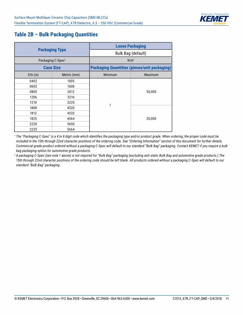
Table 2B – Bulk Packaging Quantities
Packaging TypeLoose PackagingBulk Bag (default)
Packaging C-Spec1 N/A2
Case Size Packaging Quantities (pieces/unit packaging)EIA (in) Metric (mm) Minimum Maximum
0402 1005
1
50,0000603 16080805 20121206 32161210 32251808 4520
20,0001812 45321825 45642220 56502225 5664
1 The "Packaging C-Spec" is a 4 to 8 digit code which identifies the packaging type and/or product grade. When ordering, the proper code must be included in the 15th through 22nd character positions of the ordering code. See "Ordering Information" section of this document for further details. Commercial grade product ordered without a packaging C-Spec will default to our standard "Bulk Bag" packaging. Contact KEMET if you require a bulk bag packaging option for automotive grade products.
2 A packaging C-Spec (see note 1 above) is not required for "Bulk Bag" packaging (excluding anti-static Bulk Bag and automotive grade products.) The 15th through 22nd character positions of the ordering code should be left blank. All products ordered without a packaging C-Spec will default to our standard "Bulk Bag" packaging.

© KEMET Electronics Corporation • P.O. Box 5928 • Greenville, SC 29606 • 864-963-6300 • www.kemet.com C1013_X7R_FT-CAP_SMD • 5/4/2018 12
Surface Mount Multilayer Ceramic Chip Capacitors (SMD MLCCs)Flexible Termination System (FT-CAP), X7R Dielectric, 6.3 – 250 VDC (Commercial Grade)
Table 3 – Chip Capacitor Land Pattern Design Recommendations per IPC–7351
EIA Size Code
Metric Size Code
Density Level A: Maximum (Most)
Land Protrusion (mm)
Density Level B: Median (Nominal)
Land Protrusion (mm)
Density Level C: Minimum (Least)
Land Protrusion (mm)C Y X V1 V2 C Y X V1 V2 C Y X V1 V2
0603 1608 0.85 1.25 1.10 4.00 2.10 0.75 1.05 1.00 3.10 1.50 0.65 0.85 0.90 2.40 1.20
0805 2012 0.99 1.44 1.66 4.47 2.71 0.89 1.24 1.56 3.57 2.11 0.79 1.04 1.46 2.42 1.81
1206 3216 1.59 1.62 2.06 5.85 3.06 1.49 1.42 1.96 4.95 2.46 1.39 1.22 1.86 4.25 2.16
1210 3225 1.59 1.62 3.01 5.90 4.01 1.49 1.42 2.91 4.95 3.41 1.39 1.22 2.81 4.25 3.11
1808 4520 2.30 1.75 2.30 7.40 3.30 2.20 1.55 2.20 6.50 2.70 2.10 1.35 2.10 5.80 2.40
1812 4532 2.10 1.80 3.60 7.00 4.60 2.00 1.60 3.50 6.10 4.00 1.90 1.40 3.40 5.40 3.70
1825 4564 2.15 1.80 6.90 7.10 7.90 2.05 1.60 6.80 6.20 7.30 1.95 1.40 6.70 5.50 7.00
2220 5650 2.85 2.10 5.50 8.80 6.50 2.75 1.90 5.40 7.90 5.90 2.65 1.70 5.30 7.20 5.60
2225 5664 2.85 2.10 6.90 8.80 7.90 2.75 1.90 6.80 7.90 7.30 2.65 1.70 6.70 7.20 7.00
Density Level A: For low-density product applications. Recommended for wave solder applications and provides a wider process window for reflow solder processes. KEMET only recommends wave soldering of EIA 0603, 0805, and 1206 case sizes.Density Level B: For products with a moderate level of component density. Provides a robust solder attachment condition for reflow solder processes.Density Level C: For high component density product applications. Before adapting the minimum land pattern variations, the user should perform qualification testing based on the conditions outlined in IPC Standard 7351 (IPC–7351).
Image below based on Density Level B for an EIA 1210 case size.
Y
C C
X X
V1
V2
Grid Placement Courtyard
Y

© KEMET Electronics Corporation • P.O. Box 5928 • Greenville, SC 29606 • 864-963-6300 • www.kemet.com C1013_X7R_FT-CAP_SMD • 5/4/2018 13
Surface Mount Multilayer Ceramic Chip Capacitors (SMD MLCCs)Flexible Termination System (FT-CAP), X7R Dielectric, 6.3 – 250 VDC (Commercial Grade)
Soldering Process
Recommended Soldering Technique: • Solder wave or solder reflow for EIA case sizes 0603, 0805 and 1206 • All other EIA case sizes are limited to solder reflow only
Recommended Reflow Soldering Profile:The KEMET families of surface mount multilayer ceramic capacitors (SMD MLCCs) are compatible with wave (single or dual), convection, IR or vapor phase reflow techniques. Preheating of these components is recommended to avoid extreme thermal stress. The KEMET recommended profile conditions for convection and IR reflow reflect the profile conditions of the IPC/ J-STD-020 standard for moisture sensitivity testing. These devices can safely withstand a maximum of three reflow passes at these conditions.
Profile FeatureTermination Finish
SnPb 100% Matte Sn
Preheat/SoakTemperature Minimum (TSmin) 100°C 150°CTemperature Maximum (TSmax) 150°C 200°C
Time (tS) from TSmin to TSmax 60 – 120 seconds 60 – 120 seconds
Ramp-Up Rate (TL to TP) 3°C/second maximum
3°C/second maximum
Liquidous Temperature (TL) 183°C 217°C
Time Above Liquidous (tL) 60 – 150 seconds 60 – 150 seconds
Peak Temperature (TP) 235°C 260°C
Time Within 5°C of Maximum Peak Temperature (tP)
20 seconds maximum
30 seconds maximum
Ramp-Down Rate (TP to TL)6°C/second maximum
6°C/second maximum
Time 25°C to Peak Temperature
6 minutes maximum
8 minutes maximum
Note: All temperatures refer to the center of the package, measured on the capacitor body surface that is facing up during assembly reflow.
Time
Tem
pera
ture
Tsmin
25
Tsmax
TL
TP Maximum Ramp Up Rate = 3°C/secondMaximum Ramp Down Rate = 6°C/second
tP
tL
ts
25°C to Peak
© KEMET Electronics Corporation • P.O. Box 5928 • Greenville, SC 29606 • 864-963-6300 • www.kemet.com C1013_X7R_FT-CAP_SMD • 5/4/2018 14
Surface Mount Multilayer Ceramic Chip Capacitors (SMD MLCCs)Flexible Termination System (FT-CAP), X7R Dielectric, 6.3 – 250 VDC (Commercial Grade)
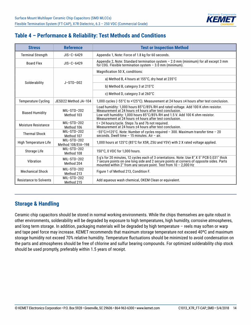
Table 4 – Performance & Reliability: Test Methods and Conditions
Stress Reference Test or Inspection MethodTerminal Strength JIS–C–6429 Appendix 1, Note: Force of 1.8 kg for 60 seconds.
Board Flex JIS–C–6429 Appendix 2, Note: Standard termination system – 2.0 mm (minimum) for all except 3 mm for C0G. Flexible termination system – 3.0 mm (minimum).
Solderability J–STD–002
Magnification 50 X, conditions:
a) Method B, 4 hours at 155°C, dry heat at 235°C
b) Method B, category 3 at 215°C
c) Method D, category 3 at 260°C
Temperature Cycling JESD22 Method JA–104 1,000 cycles (−55°C to +125°C). Measurement at 24 hours ±4 hours after test conclusion.
Biased Humidity MIL–STD–202 Method 103
Load humidity: 1,000 hours 85°C/85% RH and rated voltage. Add 100 K ohm resistor. Measurement at 24 hours ±4 hours after test conclusion.Low volt humidity: 1,000 hours 85°C/85% RH and 1.5 V. Add 100 K ohm resistor. Measurement at 24 hours ±4 hours after test conclusion.
Moisture Resistance MIL–STD–202 Method 106
t = 24 hours/cycle. Steps 7a and 7b not required.Measurement at 24 hours ±4 hours after test conclusion.
Thermal Shock MIL–STD–202 Method 107
−55°C/+125°C. Note: Number of cycles required – 300. Maximum transfer time – 20 seconds. Dwell time – 15 minutes. Air – air.
High Temperature Life MIL–STD–202 Method 108/EIA–198 1,000 hours at 125°C (85°C for X5R, Z5U and Y5V) with 2 X rated voltage applied.
Storage Life MIL–STD–202 Method 108 150°C, 0 VDC for 1,000 hours.
Vibration MIL–STD–202 Method 204
5 g's for 20 minutes, 12 cycles each of 3 orientations. Note: Use 8" X 5" PCB 0.031" thick 7 secure points on one long side and 2 secure points at corners of opposite sides. Parts mounted within 2" from any secure point. Test from 10 – 2,000 Hz
Mechanical Shock MIL–STD–202 Method 213 Figure 1 of Method 213, Condition F.
Resistance to Solvents MIL–STD–202 Method 215 Add aqueous wash chemical, OKEM Clean or equivalent.
Storage & Handling
Ceramic chip capacitors should be stored in normal working environments. While the chips themselves are quite robust in other environments, solderability will be degraded by exposure to high temperatures, high humidity, corrosive atmospheres, and long term storage. In addition, packaging materials will be degraded by high temperature – reels may soften or warp and tape peel force may increase. KEMET recommends that maximum storage temperature not exceed 40ºC and maximum storage humidity not exceed 70% relative humidity. Temperature fluctuations should be minimized to avoid condensation on the parts and atmospheres should be free of chlorine and sulfur bearing compounds. For optimized solderability chip stock should be used promptly, preferably within 1.5 years of receipt.

© KEMET Electronics Corporation • P.O. Box 5928 • Greenville, SC 29606 • 864-963-6300 • www.kemet.com C1013_X7R_FT-CAP_SMD • 5/4/2018 15
Surface Mount Multilayer Ceramic Chip Capacitors (SMD MLCCs)Flexible Termination System (FT-CAP), X7R Dielectric, 6.3 – 250 VDC (Commercial Grade)
Construction
Dielectric Material (BaTiO3)
Detailed Cross Section
Barrier Layer(Ni)
Inner Electrodes(Ni)
Termination Finish(100% Matte Sn / SnPb - 5% Pb min)
Barrier Layer(Ni)
Termination Finish(100% Matte Sn / SnPb - 5% Pb min)
Inner Electrodes(Ni)
Dielectric Material (BaTiO3)
Epoxy Layer(Ag)
Epoxy Layer(Ag)
End Termination/External Electrode
(Cu)
End Termination/External Electrode
(Cu)

© KEMET Electronics Corporation • P.O. Box 5928 • Greenville, SC 29606 • 864-963-6300 • www.kemet.com C1013_X7R_FT-CAP_SMD • 5/4/2018 16
Surface Mount Multilayer Ceramic Chip Capacitors (SMD MLCCs)Flexible Termination System (FT-CAP), X7R Dielectric, 6.3 – 250 VDC (Commercial Grade)
Capacitor Marking (Optional):These surface mount multilayer ceramic capacitors are normally supplied unmarked. If required, they can be marked as an extra cost option. Marking is available on most KEMET devices, but must be requested using the correct ordering code identifi er(s). If this option is requested, two sides of the ceramic body will be laser marked with a “K” to identify KEMET, followed by two characters (per EIA–198 - see table below) to identify the capacitance value. EIA 0603 case size devices are limited to the “K” character only.
Laser marking option is not available on:• C0G, ultra stable X8R and Y5V dielectric devices. • EIA 0402 case size devices. • EIA 0603 case size devices with fl exible termination
option.• KPS commercial and automotive grade stacked
devices.• X7R dielectric products in capacitance values outlined
below.
Marking appears in legible contrast. Illustrated below is an example of an MLCC with laser marking of “KA8”, which designates a KEMET device with rated capacitance of 100 µF. Orientation of marking is vendor optional.
KEMET ID
2-Digit Capacitance
Code
EIA Case Size Metric Size Code Capacitance0603 1608 ≤ 170 pF0805 2012 ≤ 150 pF1206 3216 ≤ 910 pF1210 3225 ≤ 2,000 pF1808 4520 ≤ 3,900 pF1812 4532 ≤ 6,700 pF1825 4564 ≤ 0.018 µF2220 5650 ≤ 0.027 µF2225 5664 ≤ 0.033 µF
© KEMET Electronics Corporation • P.O. Box 5928 • Greenville, SC 29606 • 864-963-6300 • www.kemet.com C1013_X7R_FT-CAP_SMD • 5/4/2018 17
Surface Mount Multilayer Ceramic Chip Capacitors (SMD MLCCs)Flexible Termination System (FT-CAP), X7R Dielectric, 6.3 – 250 VDC (Commercial Grade)
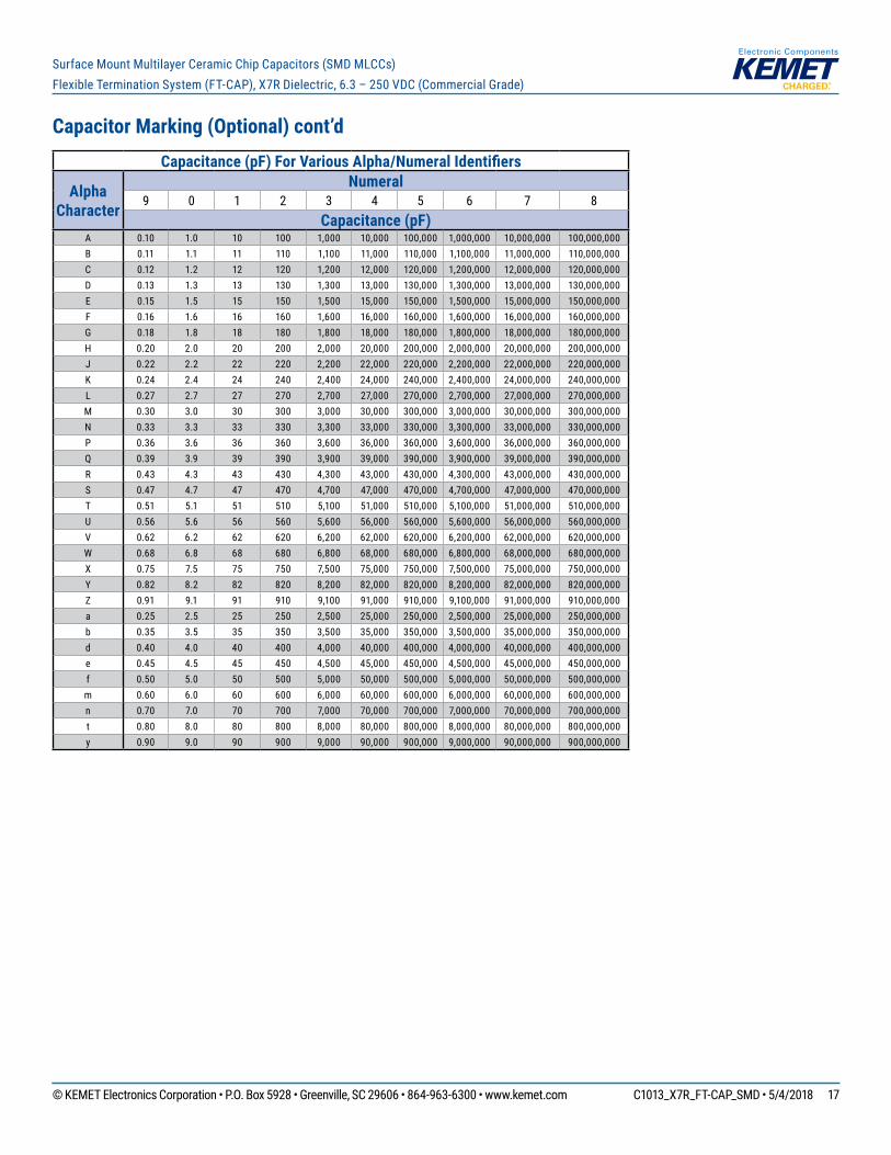
Capacitor Marking (Optional) cont’dCapacitance (pF) For Various Alpha/Numeral Identifi ers
AlphaCharacter
Numeral9 0 1 2 3 4 5 6 7 8
Capacitance (pF)A 0.10 1.0 10 100 1,000 10,000 100,000 1,000,000 10,000,000 100,000,000B 0.11 1.1 11 110 1,100 11,000 110,000 1,100,000 11,000,000 110,000,000C 0.12 1.2 12 120 1,200 12,000 120,000 1,200,000 12,000,000 120,000,000D 0.13 1.3 13 130 1,300 13,000 130,000 1,300,000 13,000,000 130,000,000E 0.15 1.5 15 150 1,500 15,000 150,000 1,500,000 15,000,000 150,000,000F 0.16 1.6 16 160 1,600 16,000 160,000 1,600,000 16,000,000 160,000,000G 0.18 1.8 18 180 1,800 18,000 180,000 1,800,000 18,000,000 180,000,000H 0.20 2.0 20 200 2,000 20,000 200,000 2,000,000 20,000,000 200,000,000J 0.22 2.2 22 220 2,200 22,000 220,000 2,200,000 22,000,000 220,000,000K 0.24 2.4 24 240 2,400 24,000 240,000 2,400,000 24,000,000 240,000,000L 0.27 2.7 27 270 2,700 27,000 270,000 2,700,000 27,000,000 270,000,000M 0.30 3.0 30 300 3,000 30,000 300,000 3,000,000 30,000,000 300,000,000N 0.33 3.3 33 330 3,300 33,000 330,000 3,300,000 33,000,000 330,000,000P 0.36 3.6 36 360 3,600 36,000 360,000 3,600,000 36,000,000 360,000,000Q 0.39 3.9 39 390 3,900 39,000 390,000 3,900,000 39,000,000 390,000,000R 0.43 4.3 43 430 4,300 43,000 430,000 4,300,000 43,000,000 430,000,000S 0.47 4.7 47 470 4,700 47,000 470,000 4,700,000 47,000,000 470,000,000T 0.51 5.1 51 510 5,100 51,000 510,000 5,100,000 51,000,000 510,000,000U 0.56 5.6 56 560 5,600 56,000 560,000 5,600,000 56,000,000 560,000,000V 0.62 6.2 62 620 6,200 62,000 620,000 6,200,000 62,000,000 620,000,000W 0.68 6.8 68 680 6,800 68,000 680,000 6,800,000 68,000,000 680,000,000X 0.75 7.5 75 750 7,500 75,000 750,000 7,500,000 75,000,000 750,000,000Y 0.82 8.2 82 820 8,200 82,000 820,000 8,200,000 82,000,000 820,000,000Z 0.91 9.1 91 910 9,100 91,000 910,000 9,100,000 91,000,000 910,000,000a 0.25 2.5 25 250 2,500 25,000 250,000 2,500,000 25,000,000 250,000,000b 0.35 3.5 35 350 3,500 35,000 350,000 3,500,000 35,000,000 350,000,000d 0.40 4.0 40 400 4,000 40,000 400,000 4,000,000 40,000,000 400,000,000e 0.45 4.5 45 450 4,500 45,000 450,000 4,500,000 45,000,000 450,000,000f 0.50 5.0 50 500 5,000 50,000 500,000 5,000,000 50,000,000 500,000,000m 0.60 6.0 60 600 6,000 60,000 600,000 6,000,000 60,000,000 600,000,000n 0.70 7.0 70 700 7,000 70,000 700,000 7,000,000 70,000,000 700,000,000t 0.80 8.0 80 800 8,000 80,000 800,000 8,000,000 80,000,000 800,000,000y 0.90 9.0 90 900 9,000 90,000 900,000 9,000,000 90,000,000 900,000,000
© KEMET Electronics Corporation • P.O. Box 5928 • Greenville, SC 29606 • 864-963-6300 • www.kemet.com C1013_X7R_FT-CAP_SMD • 5/4/2018 18
Surface Mount Multilayer Ceramic Chip Capacitors (SMD MLCCs)Flexible Termination System (FT-CAP), X7R Dielectric, 6.3 – 250 VDC (Commercial Grade)
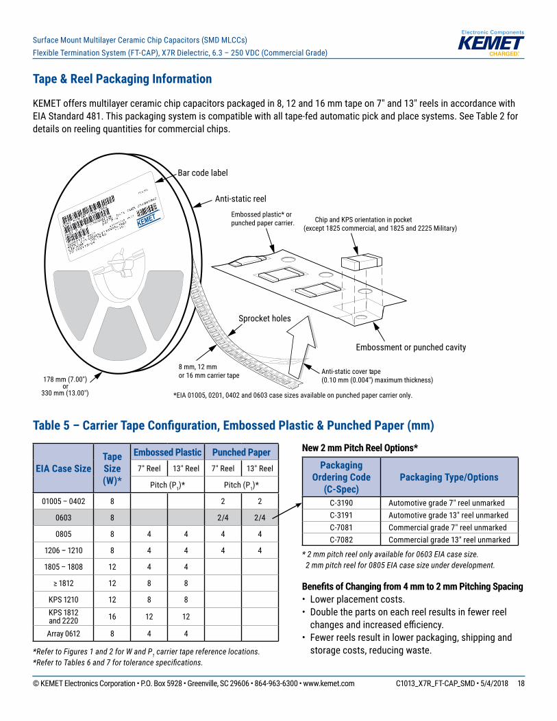
Tape & Reel Packaging Information
KEMET offers multilayer ceramic chip capacitors packaged in 8, 12 and 16 mm tape on 7" and 13" reels in accordance with EIA Standard 481. This packaging system is compatible with all tape-fed automatic pick and place systems. See Table 2 for details on reeling quantities for commercial chips.
8 mm, 12 mmor 16 mm carrier tape 178 mm (7.00")
or330 mm (13.00")
Anti-static reel
Embossed plastic* or punched paper carrier.
Embossment or punched cavity
Anti-static cover tape(0.10 mm (0.004") maximum thickness)
Chip and KPS orientation in pocket(except 1825 commercial, and 1825 and 2225 Military)
*EIA 01005, 0201, 0402 and 0603 case sizes available on punched paper carrier only.
KEMET®
Bar code label
Sprocket holes
Table 5 – Carrier Tape Confi guration, Embossed Plastic & Punched Paper (mm)
EIA Case SizeTape Size (W)*
Embossed Plastic Punched Paper7" Reel 13" Reel 7" Reel 13" Reel
Pitch (P1)* Pitch (P1)*
01005 – 0402 8 2 2
0603 8 2/4 2/4
0805 8 4 4 4 4
1206 – 1210 8 4 4 4 4
1805 – 1808 12 4 4
≥ 1812 12 8 8
KPS 1210 12 8 8KPS 1812and 2220 16 12 12
Array 0612 8 4 4
*Refer to Figures 1 and 2 for W and P1 carrier tape reference locations.*Refer to Tables 6 and 7 for tolerance specifi cations.
New 2 mm Pitch Reel Options*
PackagingOrdering Code
(C-Spec)Packaging Type/Options
C-3190 Automotive grade 7" reel unmarkedC-3191 Automotive grade 13" reel unmarkedC-7081 Commercial grade 7" reel unmarkedC-7082 Commercial grade 13" reel unmarked
* 2 mm pitch reel only available for 0603 EIA case size. 2 mm pitch reel for 0805 EIA case size under development.
Benefi ts of Changing from 4 mm to 2 mm Pitching Spacing• Lower placement costs.• Double the parts on each reel results in fewer reel
changes and increased effi ciency.• Fewer reels result in lower packaging, shipping and
storage costs, reducing waste.
© KEMET Electronics Corporation • P.O. Box 5928 • Greenville, SC 29606 • 864-963-6300 • www.kemet.com C1013_X7R_FT-CAP_SMD • 5/4/2018 19
Surface Mount Multilayer Ceramic Chip Capacitors (SMD MLCCs)Flexible Termination System (FT-CAP), X7R Dielectric, 6.3 – 250 VDC (Commercial Grade)
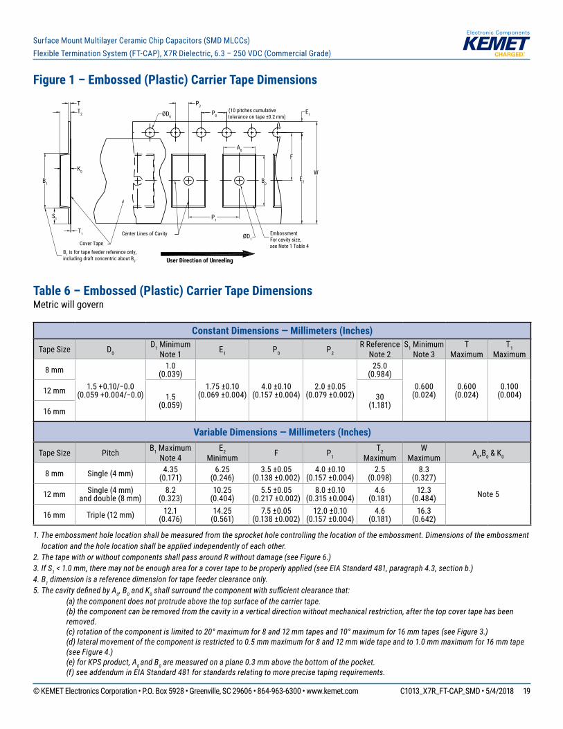
Figure 1 – Embossed (Plastic) Carrier Tape Dimensions
P0
T
F
W
Center Lines of Cavity
A0
B0
User Direction of Unreeling
Cover Tape
K0
B1 is for tape feeder reference only, including draft concentric about B0.
T2
ØD1
ØD0
B1
S1
T1
E1
E2
P1
P2
EmbossmentFor cavity size,see Note 1 Table 4
(10 pitches cumulativetolerance on tape ±0.2 mm)
Table 6 – Embossed (Plastic) Carrier Tape DimensionsMetric will govern
Constant Dimensions — Millimeters (Inches)
Tape Size D0 D1 Minimum
Note 1 E1 P0 P2 R Reference
Note 2S1 Minimum
Note 3T
MaximumT1
Maximum
8 mm
1.5 +0.10/−0.0 (0.059 +0.004/−0.0)
1.0 (0.039)
1.75 ±0.10 (0.069 ±0.004)
4.0 ±0.10 (0.157 ±0.004)
2.0 ±0.05(0.079 ±0.002)
25.0 (0.984)
0.600 (0.024)
0.600 (0.024)
0.100 (0.004)12 mm
1.5 (0.059)
30 (1.181)
16 mm
Variable Dimensions — Millimeters (Inches)
Tape Size Pitch B1 MaximumNote 4
E2 Minimum F P1
T2 Maximum
W Maximum A0,B0 & K0
8 mm Single (4 mm) 4.35 (0.171)
6.25 (0.246)
3.5 ±0.05 (0.138 ±0.002)
4.0 ±0.10(0.157 ±0.004)
2.5 (0.098)
8.3 (0.327)
Note 512 mm Single (4 mm)and double (8 mm)
8.2 (0.323)
10.25 (0.404)
5.5 ±0.05 (0.217 ±0.002)
8.0 ±0.10(0.315 ±0.004)
4.6 (0.181)
12.3 (0.484)
16 mm Triple (12 mm) 12.1 (0.476)
14.25(0.561)
7.5 ±0.05(0.138 ±0.002)
12.0 ±0.10(0.157 ±0.004)
4.6 (0.181)
16.3 (0.642)
1. The embossment hole location shall be measured from the sprocket hole controlling the location of the embossment. Dimensions of the embossment location and the hole location shall be applied independently of each other.
2. The tape with or without components shall pass around R without damage (see Figure 6.)3. If S1 < 1.0 mm, there may not be enough area for a cover tape to be properly applied (see EIA Standard 481, paragraph 4.3, section b.)4. B1 dimension is a reference dimension for tape feeder clearance only.5. The cavity defi ned by A0, B0 and K0 shall surround the component with suffi cient clearance that: (a) the component does not protrude above the top surface of the carrier tape. (b) the component can be removed from the cavity in a vertical direction without mechanical restriction, after the top cover tape has been
removed. (c) rotation of the component is limited to 20° maximum for 8 and 12 mm tapes and 10° maximum for 16 mm tapes (see Figure 3.) (d) lateral movement of the component is restricted to 0.5 mm maximum for 8 and 12 mm wide tape and to 1.0 mm maximum for 16 mm tape
(see Figure 4.) (e) for KPS product, A0 and B0 are measured on a plane 0.3 mm above the bottom of the pocket. (f) see addendum in EIA Standard 481 for standards relating to more precise taping requirements.
© KEMET Electronics Corporation • P.O. Box 5928 • Greenville, SC 29606 • 864-963-6300 • www.kemet.com C1013_X7R_FT-CAP_SMD • 5/4/2018 20
Surface Mount Multilayer Ceramic Chip Capacitors (SMD MLCCs)Flexible Termination System (FT-CAP), X7R Dielectric, 6.3 – 250 VDC (Commercial Grade)
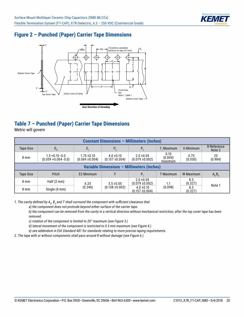
Figure 2 – Punched (Paper) Carrier Tape Dimensions
User Direction of Unreeling
Top Cover Tape
T
Center Lines of Cavity
P1
ØDo Po E1
F
E2
W
G
A0
B0
Cavity Size,SeeNote 1, Table 7
Bottom Cover Tape
T1
T1
Bottom Cover Tape
(10 pitches cumulativetolerance on tape ±0.2 mm)
Table 7 – Punched (Paper) Carrier Tape Dimensions Metric will govern
Constant Dimensions — Millimeters (Inches)Tape Size D0 E1 P0 P2 T1 Maximum G Minimum R Reference
Note 2
8 mm 1.5 +0.10 -0.0 (0.059 +0.004 -0.0)
1.75 ±0.10 (0.069 ±0.004)
4.0 ±0.10 (0.157 ±0.004)
2.0 ±0.05 (0.079 ±0.002)
0.10 (0.004)
maximum0.75
(0.030) 25
(0.984)
Variable Dimensions — Millimeters (Inches)Tape Size Pitch E2 Minimum F P1 T Maximum W Maximum A0 B0
8 mm Half (2 mm) 6.25 (0.246)
3.5 ±0.05 (0.138 ±0.002)
2.0 ±0.05 (0.079 ±0.002) 1.1
(0.098)
8.3(0.327) Note 1
8 mm Single (4 mm) 4.0 ±0.10 (0.157 ±0.004)
8.3(0.327)
1. The cavity defi ned by A0, B0 and T shall surround the component with suffi cient clearance that: a) the component does not protrude beyond either surface of the carrier tape. b) the component can be removed from the cavity in a vertical direction without mechanical restriction, after the top cover tape has been
removed. c) rotation of the component is limited to 20° maximum (see Figure 3.) d) lateral movement of the component is restricted to 0.5 mm maximum (see Figure 4.) e) see addendum in EIA Standard 481 for standards relating to more precise taping requirements.2. The tape with or without components shall pass around R without damage (see Figure 6.)
© KEMET Electronics Corporation • P.O. Box 5928 • Greenville, SC 29606 • 864-963-6300 • www.kemet.com C1013_X7R_FT-CAP_SMD • 5/4/2018 21
Surface Mount Multilayer Ceramic Chip Capacitors (SMD MLCCs)Flexible Termination System (FT-CAP), X7R Dielectric, 6.3 – 250 VDC (Commercial Grade)
Packaging Information Performance Notes
1. Cover Tape Break Force: 1.0 kg minimum.2. Cover Tape Peel Strength: The total peel strength of the cover tape from the carrier tape shall be:
Tape Width Peel Strength8 mm 0.1 to 1.0 newton (10 to 100 gf)
12 and 16 mm 0.1 to 1.3 newton (10 to 130 gf)
The direction of the pull shall be opposite the direction of the carrier tape travel. The pull angle of the carrier tape shall be 165° to 180° from the plane of the carrier tape. During peeling, the carrier and/or cover tape shall be pulled at a velocity of 300 ±10 mm/minute.3. Labeling: Bar code labeling (standard or custom) shall be on the side of the reel opposite the sprocket holes. Refer to EIA Standards 556 and 624.
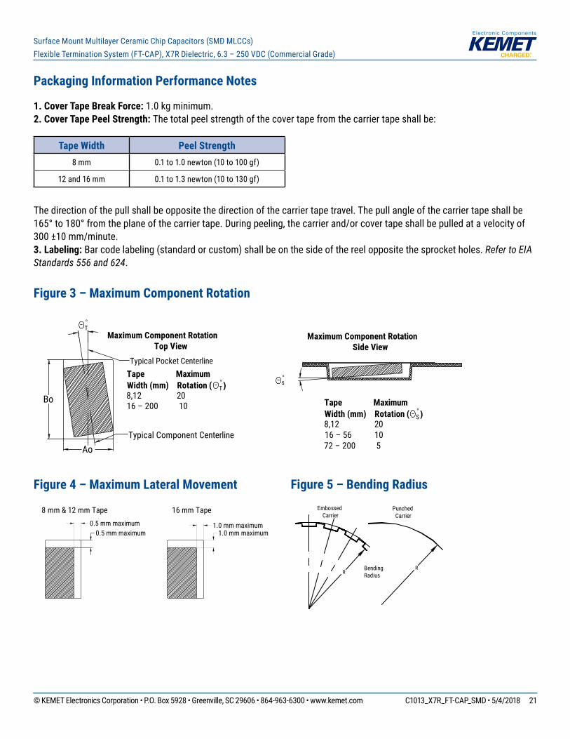
Figure 3 – Maximum Component Rotation
Ao
Bo
°T
°s
Maximum Component RotationTop View
Maximum Component RotationSide View
Tape MaximumWidth (mm) Rotation ( °
T)8,12 20 16 – 200 10 Tape Maximum
Width (mm) Rotation ( °S)
8,12 20 16 – 56 1072 – 200 5
Typical Pocket Centerline
Typical Component Centerline
Figure 4 – Maximum Lateral Movement
0.5 mm maximum0.5 mm maximum
8 mm & 12 mm Tape
1.0 mm maximum1.0 mm maximum
16 mm Tape
Figure 5 – Bending Radius
RRBending
Radius
EmbossedCarrier
PunchedCarrier
© KEMET Electronics Corporation • P.O. Box 5928 • Greenville, SC 29606 • 864-963-6300 • www.kemet.com C1013_X7R_FT-CAP_SMD • 5/4/2018 22
Surface Mount Multilayer Ceramic Chip Capacitors (SMD MLCCs)Flexible Termination System (FT-CAP), X7R Dielectric, 6.3 – 250 VDC (Commercial Grade)
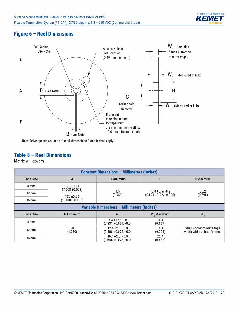
Figure 6 – Reel Dimensions
A D (See Note)
Full Radius,See Note
B (see Note)
Access Hole atSlot Location(Ø 40 mm minimum)
If present,tape slot in corefor tape start:2.5 mm minimum width x10.0 mm minimum depth
W3 (Includes flange distortion at outer edge)
W2 (Measured at hub)
W1 (Measured at hub)
C(Arbor holediameter)
Note: Drive spokes optional; if used, dimensions B and D shall apply.
N
Table 8 – Reel DimensionsMetric will govern
Constant Dimensions — Millimeters (Inches) Tape Size A B Minimum C D Minimum
8 mm 178 ±0.20 (7.008 ±0.008)
or330 ±0.20
(13.000 ±0.008)
1.5 (0.059)
13.0 +0.5/−0.2 (0.521 +0.02/−0.008)
20.2 (0.795)12 mm
16 mm
Variable Dimensions — Millimeters (Inches) Tape Size N Minimum W1 W2 Maximum W3
8 mm
50 (1.969)
8.4 +1.5/−0.0(0.331 +0.059/−0.0)
14.4 (0.567)
Shall accommodate tape width without interference12 mm 12.4 +2.0/−0.0
(0.488 +0.078/−0.0) 18.4
(0.724)
16 mm 16.4 +2.0/−0.0(0.646 +0.078/−0.0)
22.4 (0.882)

© KEMET Electronics Corporation • P.O. Box 5928 • Greenville, SC 29606 • 864-963-6300 • www.kemet.com C1013_X7R_FT-CAP_SMD • 5/4/2018 23
Surface Mount Multilayer Ceramic Chip Capacitors (SMD MLCCs)Flexible Termination System (FT-CAP), X7R Dielectric, 6.3 – 250 VDC (Commercial Grade)
Figure 7 – Tape Leader & Trailer Dimensions
Trailer160 mm minimum
Carrier Tape
END STARTRound Sprocket Holes
Elongated Sprocket Holes(32 mm tape and wider)
Top Cover Tape
Top Cover Tape
Punched Carrier8 mm & 12 mm only
Embossed Carrier
Components
100 mm minimum leader
400 mm minimum
Figure 8 – Maximum Camber
Carrier TapeRound Sprocket Holes
1 mm maximum, either direction
Straight Edge
250 mm
Elongated Sprocket Holes(32 mm & wider tapes)
© KEMET Electronics Corporation • P.O. Box 5928 • Greenville, SC 29606 • 864-963-6300 • www.kemet.com C1013_X7R_FT-CAP_SMD • 5/4/2018 24
Surface Mount Multilayer Ceramic Chip Capacitors (SMD MLCCs)Flexible Termination System (FT-CAP), X7R Dielectric, 6.3 – 250 VDC (Commercial Grade)
KEMET Electronics Corporation Sales Offi ces
For a complete list of our global sales offi ces, please visit www.kemet.com/sales.
DisclaimerAll product specifi cations, statements, information and data (collectively, the “Information”) in this datasheet are subject to change. The customer is responsible for checking and verifying the extent to which the Information contained in this publication is applicable to an order at the time the order is placed.
All Information given herein is believed to be accurate and reliable, but it is presented without guarantee, warranty, or responsibility of any kind, expressed or implied.
Statements of suitability for certain applications are based on KEMET Electronics Corporation’s (“KEMET”) knowledge of typical operating conditions for such applications, but are not intended to constitute – and KEMET specifi cally disclaims – any warranty concerning suitability for a specifi c customer application or use. The Information is intended for use only by customers who have the requisite experience and capability to determine the correct products for their application. Any technical advice inferred from this Information or otherwise provided by KEMET with reference to the use of KEMET’s products is given gratis, and KEMET assumes no obligation or liability for the advice given or results obtained.
Although KEMET designs and manufactures its products to the most stringent quality and safety standards, given the current state of the art, isolated component failures may still occur. Accordingly, customer applications which require a high degree of reliability or safety should employ suitable designs or other safeguards (such as installation of protective circuitry or redundancies) in order to ensure that the failure of an electrical component does not result in a risk of personal injury or property damage.
Although all product–related warnings, cautions and notes must be observed, the customer should not assume that all safety measures are indicted or that other measures may not be required.
KEMET is a registered trademark of KEMET Electronics Corporation.