Embed Size (px)
Citation preview
Unictron Technologies Corporation Website:www.unictron.com
THIS DRAWINGS AND SPECIFICATIONS ARE THE PROPERTY OF UNICTRON TECHNOLOGIES CORPORATION AND SHALL NOT BE REPRODUCED OR USED AS THE BASIS FOR THE MANUFACTURE OR SALE OF APPARATUS OR DEVICES WITHOUT PERMISSION
Prepared by : Jane Designed by : Tom Checked by : Mike Approved by Herbert
TITLE 40.0 x 5.0 x 6.0 (mm) LTE Full-Band Ceramic Chip Antenna (CC40D9) Engineering Specification
DOCUMENT H2UE3P1D2G0100
REV.
NO. G
PAGE 1 OF 16
H 2 1 3 P D G 1 0U E 0 2 0
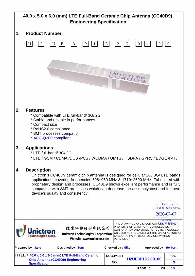
40.0 x 5.0 x 6.0 (mm) LTE Full-Band Ceramic Chip Antenna (CC40D9) Engineering Specification
1. Product Number
2. Features * Compatible with LTE full-band/ 3G/ 2G * Stable and reliable in performances * Compact size * RoHS2.0 compliance * SMT processes compatib * AEC-Q* AEC-Q200 compliant 3. Applications * LTE full-band/ 3G/ 2G. * LTE / GSM / CDMA /DCS /PCS / WCDMA / UMTS / HSDPA / GPRS / EDGE /IMT.
4. Description Unictron’s CC40D9 ceramic chip antenna is designed for cellular 2G/ 3G/ LTE bands applications, covering frequencies 698~960 MHz & 1710~2690 MHz. Fabricated with proprietary design and processes, CC40D9 shows excellent performance and is fully compatible with SMT processes which can decrease the assembly cost and improve device’s quality and consistency. 2020-07-07
Unictron Technologies Corp.
Document Control Center
Unictron Technologies Corporation Website:www.unictron.com
THIS DRAWINGS AND SPECIFICATIONS ARE THE PROPERTY OF UNICTRON TECHNOLOGIES CORPORATION AND SHALL NOT BE REPRODUCED OR USED AS THE BASIS FOR THE MANUFACTURE OR SALE OF APPARATUS OR DEVICES WITHOUT PERMISSION
Prepared by : Jane Designed by : Tom Checked by : Mike Approved by Herbert
TITLE 40.0 x 5.0 x 6.0 (mm) LTE Full-Band Ceramic Chip Antenna (CC40D9) Engineering Specification
DOCUMENT H2UE3P1D2G0100
REV.
NO. G
PAGE 2 OF 16
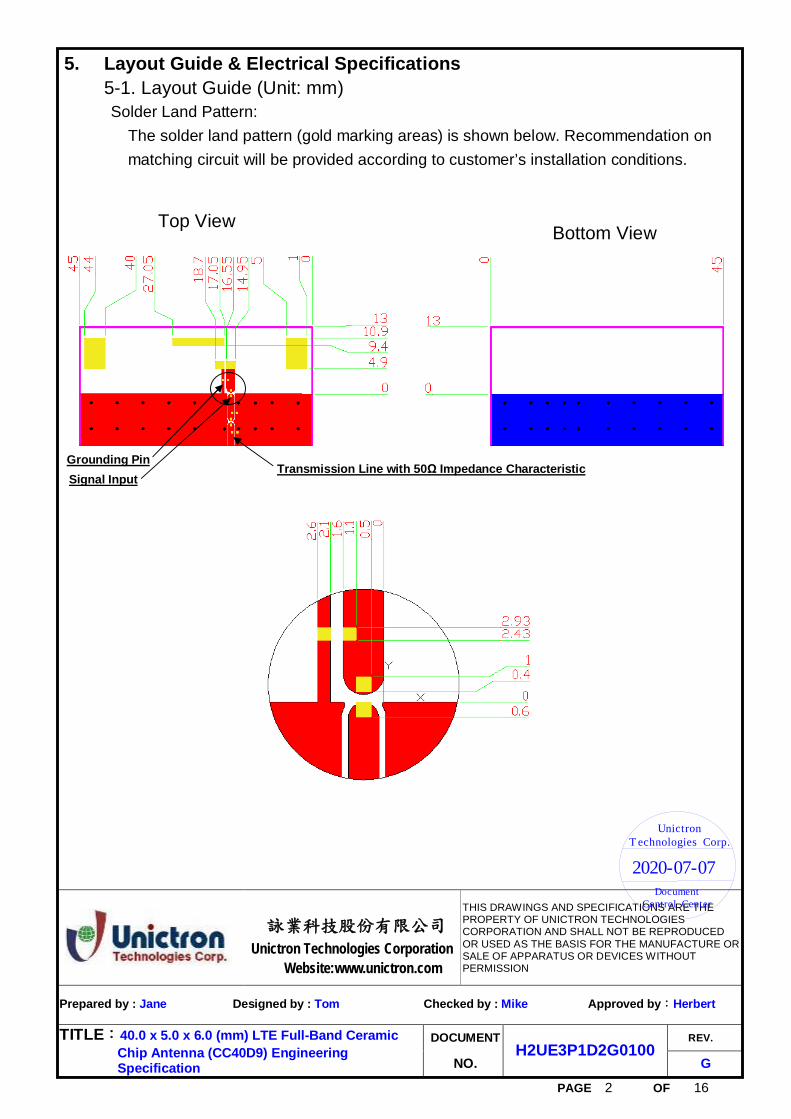
5. Layout Guide & Electrical Specifications 5-1. Layout Guide (Unit: mm)
Solder Land Pattern: The solder land pattern (gold marking areas) is shown below. Recommendation on matching circuit will be provided according to customer’s installation conditions.
Grounding Pin Signal Input
Transmission Line with 50 Impedance Characteristic
Top View Bottom View
2020-07-07
Unictron Technologies Corp.
Document Control Center
Unictron Technologies Corporation Website:www.unictron.com
THIS DRAWINGS AND SPECIFICATIONS ARE THE PROPERTY OF UNICTRON TECHNOLOGIES CORPORATION AND SHALL NOT BE REPRODUCED OR USED AS THE BASIS FOR THE MANUFACTURE OR SALE OF APPARATUS OR DEVICES WITHOUT PERMISSION
Prepared by : Jane Designed by : Tom Checked by : Mike Approved by Herbert
TITLE 40.0 x 5.0 x 6.0 (mm) LTE Full-Band Ceramic Chip Antenna (CC40D9) Engineering Specification
DOCUMENT H2UE3P1D2G0100
REV.
NO. G
PAGE 3 OF 16
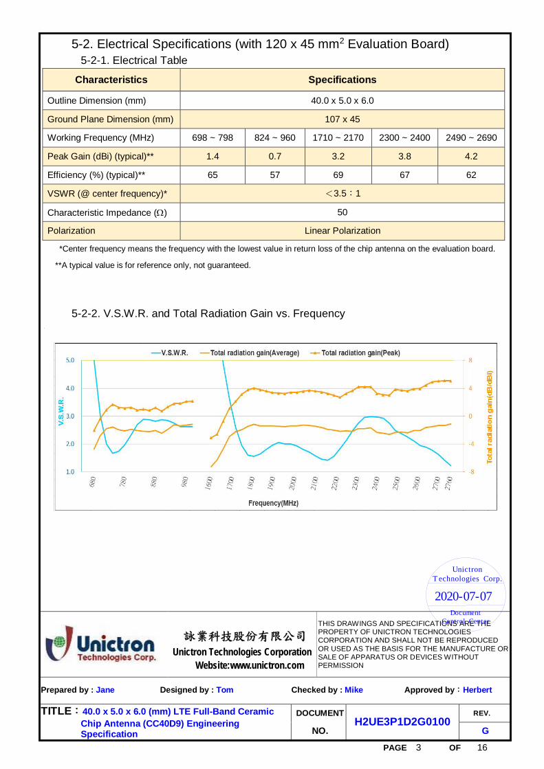
5-2. Electrical Specifications (with 120 x 45 mm2 Evaluation Board) 5-2-1. Electrical Table
Characteristics Specifications
Outline Dimension (mm) 40.0 x 5.0 x 6.0
Ground Plane Dimension (mm) 107 x 45
Working Frequency (MHz) 698 ~ 798 824 ~ 960 1710 ~ 2170 2300 ~ 2400 2490 ~ 2690
Peak Gain (dBi) (typical)** 1.4 0.7 3.2 3.8 4.2
Efficiency (%) (typical)** 65 57 69 67 62
VSWR (@ center frequency)* 3.5 1
Characteristic Impedance ( ) 50
Polarization Linear Polarization
*Center frequency means the frequency with the lowest value in return loss of the chip antenna on the evaluation board. **A typical value is for reference only, not guaranteed.
5-2-2. V.S.W.R. and Total Radiation Gain vs. Frequency
2020-07-07
Unictron Technologies Corp.
Document Control Center
Unictron Technologies Corporation Website:www.unictron.com
THIS DRAWINGS AND SPECIFICATIONS ARE THE PROPERTY OF UNICTRON TECHNOLOGIES CORPORATION AND SHALL NOT BE REPRODUCED OR USED AS THE BASIS FOR THE MANUFACTURE OR SALE OF APPARATUS OR DEVICES WITHOUT PERMISSION
Prepared by : Jane Designed by : Tom Checked by : Mike Approved by Herbert
TITLE 40.0 x 5.0 x 6.0 (mm) LTE Full-Band Ceramic Chip Antenna (CC40D9) Engineering Specification
DOCUMENT H2UE3P1D2G0100
REV.
NO. G
PAGE 4 OF 16
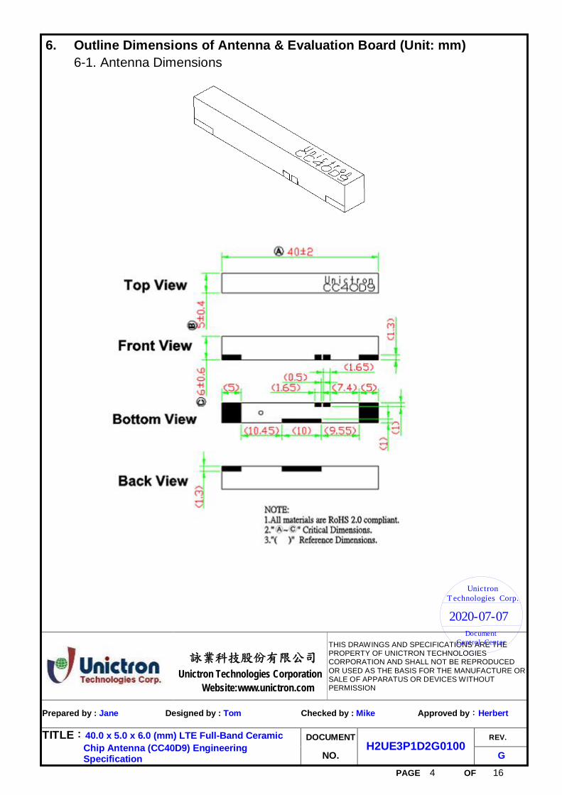
6. Outline Dimensions of Antenna & Evaluation Board (Unit: mm) 6-1. Antenna Dimensions
2020-07-07
Unictron Technologies Corp.
Document Control Center
Unictron Technologies Corporation Website:www.unictron.com
THIS DRAWINGS AND SPECIFICATIONS ARE THE PROPERTY OF UNICTRON TECHNOLOGIES CORPORATION AND SHALL NOT BE REPRODUCED OR USED AS THE BASIS FOR THE MANUFACTURE OR SALE OF APPARATUS OR DEVICES WITHOUT PERMISSION
Prepared by : Jane Designed by : Tom Checked by : Mike Approved by Herbert
TITLE 40.0 x 5.0 x 6.0 (mm) LTE Full-Band Ceramic Chip Antenna (CC40D9) Engineering Specification
DOCUMENT H2UE3P1D2G0100
REV.
NO. G
PAGE 5 OF 16
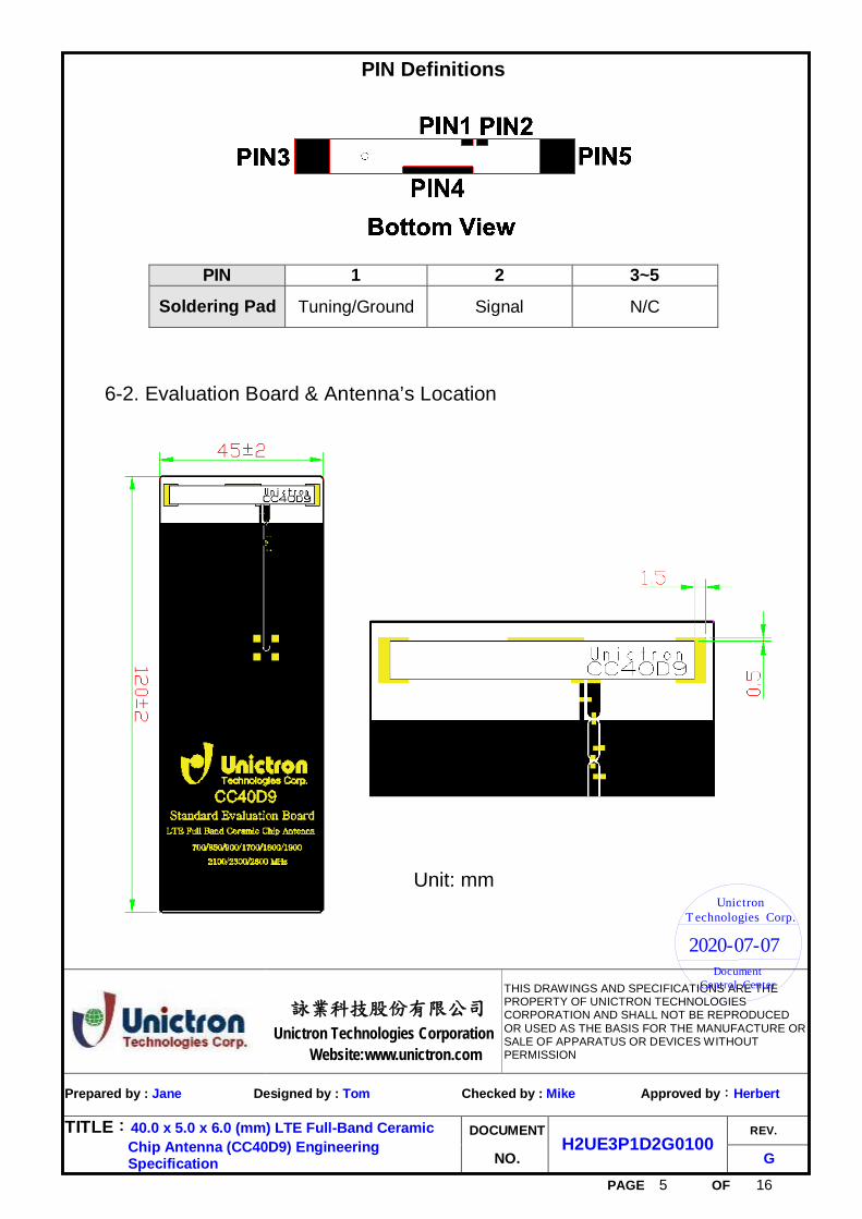
PIN Definitions
PIN 1 2 3~5
Soldering Pad Tuning/Ground Signal N/C
6-2. Evaluation Board & Antenna’s Location
Unit: mm
2020-07-07
Unictron Technologies Corp.
Document Control Center
Unictron Technologies Corporation Website:www.unictron.com
THIS DRAWINGS AND SPECIFICATIONS ARE THE PROPERTY OF UNICTRON TECHNOLOGIES CORPORATION AND SHALL NOT BE REPRODUCED OR USED AS THE BASIS FOR THE MANUFACTURE OR SALE OF APPARATUS OR DEVICES WITHOUT PERMISSION
Prepared by : Jane Designed by : Tom Checked by : Mike Approved by Herbert
TITLE 40.0 x 5.0 x 6.0 (mm) LTE Full-Band Ceramic Chip Antenna (CC40D9) Engineering Specification
DOCUMENT H2UE3P1D2G0100
REV.
NO. G
PAGE 6 OF 16
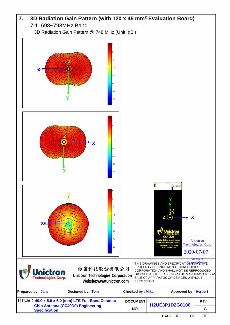
7. 3D Radiation Gain Pattern (with 120 x 45 mm2 Evaluation Board) 7-1. 698~798MHz Band
3D Radiation Gain Pattern @ 748 MHz (Unit: dBi)
X
Y
Z
Y
XZ
Y
Z
XZ
Y
X
2020-07-07
Unictron Technologies Corp.
Document Control Center

Unictron Technologies Corporation Website:www.unictron.com
THIS DRAWINGS AND SPECIFICATIONS ARE THE PROPERTY OF UNICTRON TECHNOLOGIES CORPORATION AND SHALL NOT BE REPRODUCED OR USED AS THE BASIS FOR THE MANUFACTURE OR SALE OF APPARATUS OR DEVICES WITHOUT PERMISSION
Prepared by : Jane Designed by : Tom Checked by : Mike Approved by Herbert
TITLE 40.0 x 5.0 x 6.0 (mm) LTE Full-Band Ceramic Chip Antenna (CC40D9) Engineering Specification
DOCUMENT H2UE3P1D2G0100
REV.
NO. G
PAGE 7 OF 16
7-2. 824~960MHz Band 3D Radiation Gain Pattern @ 900 MHz (Unit: dBi)
X
Y
Z
Y
XZ
Y
Z
XZ
Y
X
2020-07-07
Unictron Technologies Corp.
Document Control Center

Unictron Technologies Corporation Website:www.unictron.com
THIS DRAWINGS AND SPECIFICATIONS ARE THE PROPERTY OF UNICTRON TECHNOLOGIES CORPORATION AND SHALL NOT BE REPRODUCED OR USED AS THE BASIS FOR THE MANUFACTURE OR SALE OF APPARATUS OR DEVICES WITHOUT PERMISSION
Prepared by : Jane Designed by : Tom Checked by : Mike Approved by Herbert
TITLE 40.0 x 5.0 x 6.0 (mm) LTE Full-Band Ceramic Chip Antenna (CC40D9) Engineering Specification
DOCUMENT H2UE3P1D2G0100
REV.
NO. G
PAGE 8 OF 16
7-3. 1710~2170MHz Band 3D Radiation Gain Pattern @ 1950 MHz (Unit: dBi)
X
Y
Z
Y
XZ
Y
Z
XZ
Y
X
2020-07-07
Unictron Technologies Corp.
Document Control Center
Unictron Technologies Corporation Website:www.unictron.com
THIS DRAWINGS AND SPECIFICATIONS ARE THE PROPERTY OF UNICTRON TECHNOLOGIES CORPORATION AND SHALL NOT BE REPRODUCED OR USED AS THE BASIS FOR THE MANUFACTURE OR SALE OF APPARATUS OR DEVICES WITHOUT PERMISSION
Prepared by : Jane Designed by : Tom Checked by : Mike Approved by Herbert
TITLE 40.0 x 5.0 x 6.0 (mm) LTE Full-Band Ceramic Chip Antenna (CC40D9) Engineering Specification
DOCUMENT H2UE3P1D2G0100
REV.
NO. G
PAGE 9 OF 16
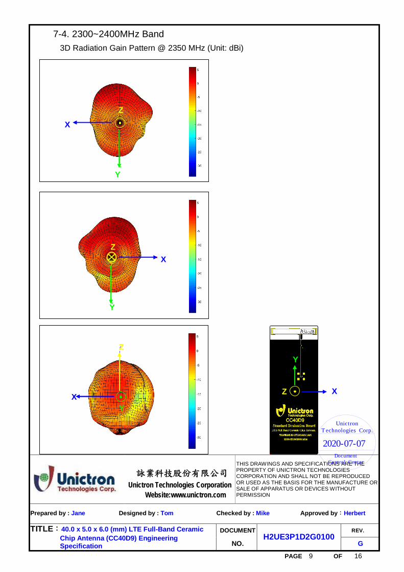
7-4. 2300~2400MHz Band 3D Radiation Gain Pattern @ 2350 MHz (Unit: dBi)
X
Y
Z
Y
XZ
Y
Z
X Z
Y
X
2020-07-07
Unictron Technologies Corp.
Document Control Center
Unictron Technologies Corporation Website:www.unictron.com
THIS DRAWINGS AND SPECIFICATIONS ARE THE PROPERTY OF UNICTRON TECHNOLOGIES CORPORATION AND SHALL NOT BE REPRODUCED OR USED AS THE BASIS FOR THE MANUFACTURE OR SALE OF APPARATUS OR DEVICES WITHOUT PERMISSION
Prepared by : Jane Designed by : Tom Checked by : Mike Approved by Herbert
TITLE 40.0 x 5.0 x 6.0 (mm) LTE Full-Band Ceramic Chip Antenna (CC40D9) Engineering Specification
DOCUMENT H2UE3P1D2G0100
REV.
NO. G
PAGE 10 OF 16
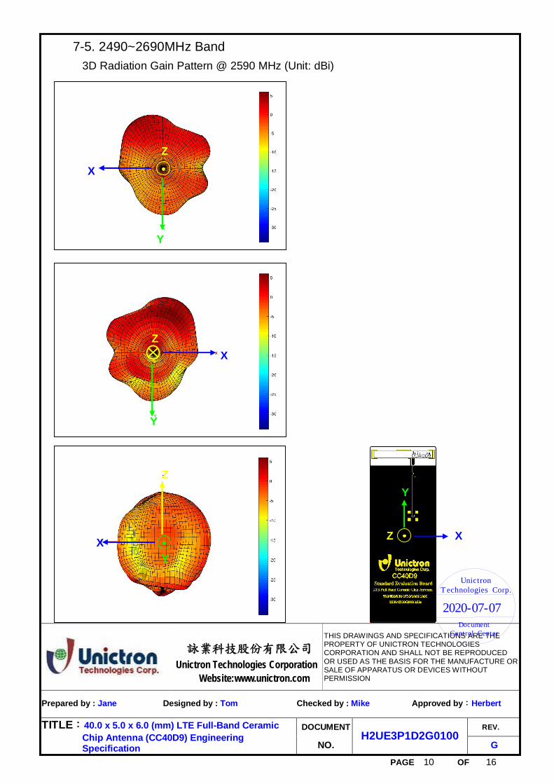
7-5. 2490~2690MHz Band 3D Radiation Gain Pattern @ 2590 MHz (Unit: dBi)
X
Y
Z
Y
XZ
Y
Z
X Z
Y
X
2020-07-07
Unictron Technologies Corp.
Document Control Center
Unictron Technologies Corporation Website:www.unictron.com
THIS DRAWINGS AND SPECIFICATIONS ARE THE PROPERTY OF UNICTRON TECHNOLOGIES CORPORATION AND SHALL NOT BE REPRODUCED OR USED AS THE BASIS FOR THE MANUFACTURE OR SALE OF APPARATUS OR DEVICES WITHOUT PERMISSION
Prepared by : Jane Designed by : Tom Checked by : Mike Approved by Herbert
TITLE 40.0 x 5.0 x 6.0 (mm) LTE Full-Band Ceramic Chip Antenna (CC40D9) Engineering Specification
DOCUMENT H2UE3P1D2G0100
REV.
NO. G
PAGE 11 OF 16
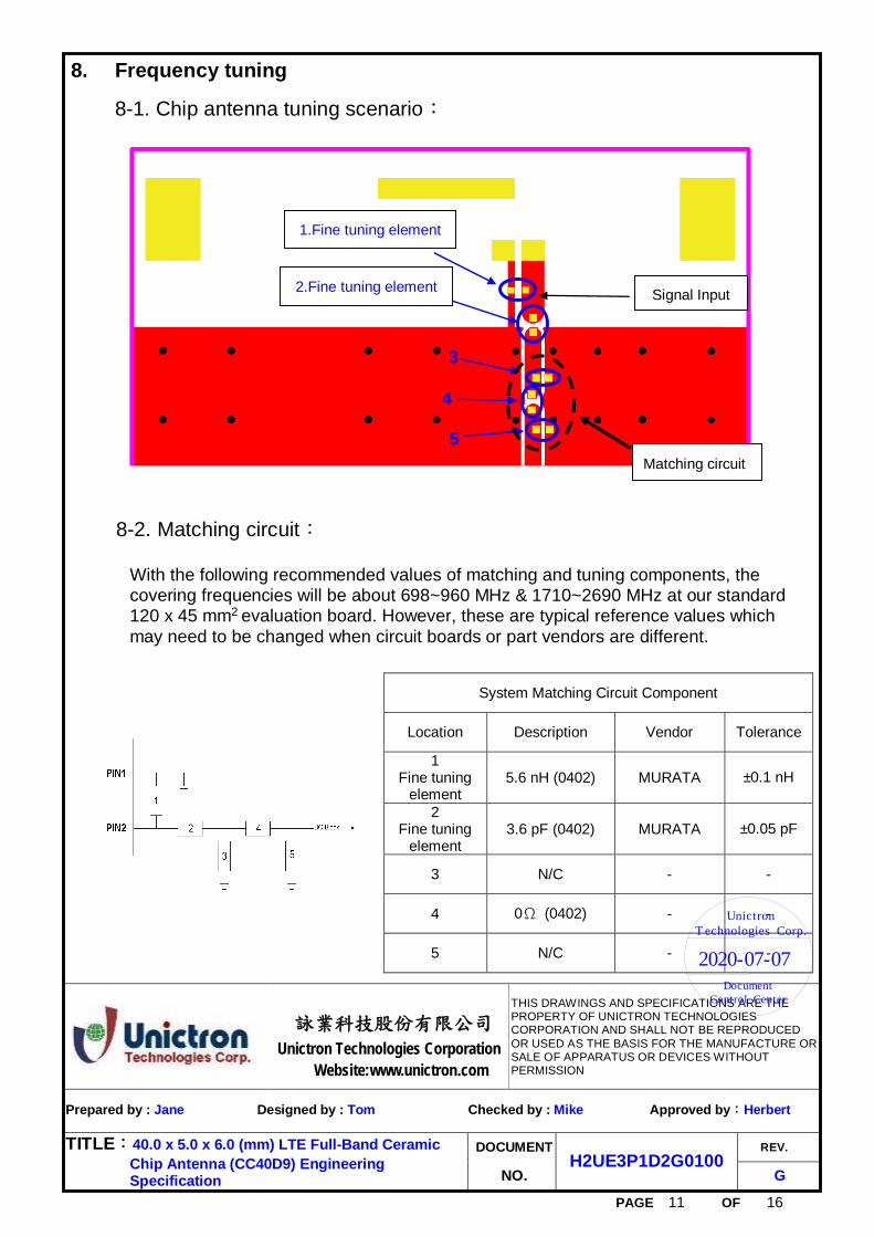
8. Frequency tuning
8-1. Chip antenna tuning scenario
8-2. Matching circuit With the following recommended values of matching and tuning components, the covering frequencies will be about 698~960 MHz & 1710~2690 MHz at our standard 120 x 45 mm2 evaluation board. However, these are typical reference values which may need to be changed when circuit boards or part vendors are different.
System Matching Circuit Component
Location Description Vendor Tolerance
1 Fine tuning
element 5.6 nH (0402) MURATA ±0.1 nH
2 Fine tuning
element 3.6 pF (0402) MURATA ±0.05 pF
3 N/C - -
4 0 (0402) - -
5 N/C - -
Signal Input
Matching circuit
3
1.Fine tuning element
4
5
2.Fine tuning element
2020-07-07
Unictron Technologies Corp.
Document Control Center
Unictron Technologies Corporation Website:www.unictron.com
THIS DRAWINGS AND SPECIFICATIONS ARE THE PROPERTY OF UNICTRON TECHNOLOGIES CORPORATION AND SHALL NOT BE REPRODUCED OR USED AS THE BASIS FOR THE MANUFACTURE OR SALE OF APPARATUS OR DEVICES WITHOUT PERMISSION
Prepared by : Jane Designed by : Tom Checked by : Mike Approved by Herbert
TITLE 40.0 x 5.0 x 6.0 (mm) LTE Full-Band Ceramic Chip Antenna (CC40D9) Engineering Specification
DOCUMENT H2UE3P1D2G0100
REV.
NO. G
PAGE 12 OF 16
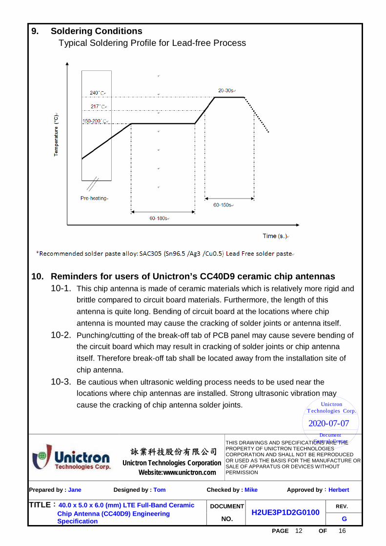
9. Soldering Conditions Typical Soldering Profile for Lead-free Process
10. Reminders for users of Unictron’s CC40D9 ceramic chip antennas 10-1. This chip antenna is made of ceramic materials which is relatively more rigid and
brittle compared to circuit board materials. Furthermore, the length of this antenna is quite long. Bending of circuit board at the locations where chip antenna is mounted may cause the cracking of solder joints or antenna itself.
10-2. Punching/cutting of the break-off tab of PCB panel may cause severe bending of the circuit board which may result in cracking of solder joints or chip antenna itself. Therefore break-off tab shall be located away from the installation site of chip antenna.
10-3. Be cautious when ultrasonic welding process needs to be used near the locations where chip antennas are installed. Strong ultrasonic vibration may cause the cracking of chip antenna solder joints.
2020-07-07
Unictron Technologies Corp.
Document Control Center
Unictron Technologies Corporation Website:www.unictron.com
THIS DRAWINGS AND SPECIFICATIONS ARE THE PROPERTY OF UNICTRON TECHNOLOGIES CORPORATION AND SHALL NOT BE REPRODUCED OR USED AS THE BASIS FOR THE MANUFACTURE OR SALE OF APPARATUS OR DEVICES WITHOUT PERMISSION
Prepared by : Jane Designed by : Tom Checked by : Mike Approved by Herbert
TITLE 40.0 x 5.0 x 6.0 (mm) LTE Full-Band Ceramic Chip Antenna (CC40D9) Engineering Specification
DOCUMENT H2UE3P1D2G0100
REV.
NO. G
PAGE 13 OF 16
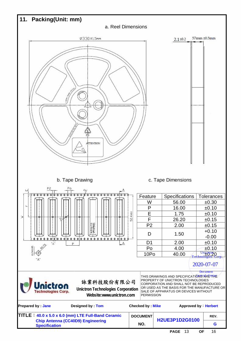
11. Packing(Unit: mm) a. Reel Dimensions
b. Tape Drawing c. Tape Dimensions
Feature Specifications Tolerances
W 56.00 ±0.30 P 16.00 ±0.10 E 1.75 ±0.10 F 26.20 ±0.15
P2 2.00 ±0.15
D 1.50 +0.10 -0.00
D1 2.00 ±0.10 Po 4.00 ±0.10
10Po 40.00 ±0.20
2020-07-07
Unictron Technologies Corp.
Document Control Center
Unictron Technologies Corporation Website:www.unictron.com
THIS DRAWINGS AND SPECIFICATIONS ARE THE PROPERTY OF UNICTRON TECHNOLOGIES CORPORATION AND SHALL NOT BE REPRODUCED OR USED AS THE BASIS FOR THE MANUFACTURE OR SALE OF APPARATUS OR DEVICES WITHOUT PERMISSION
Prepared by : Jane Designed by : Tom Checked by : Mike Approved by Herbert
TITLE 40.0 x 5.0 x 6.0 (mm) LTE Full-Band Ceramic Chip Antenna (CC40D9) Engineering Specification
DOCUMENT H2UE3P1D2G0100
REV.
NO. G
PAGE 14 OF 16
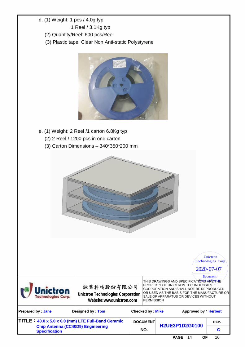
d. (1) Weight: 1 pcs / 4.0g typ 1 Reel / 3.1Kg typ
(2) Quantity/Reel: 600 pcs/Reel (3) Plastic tape: Clear Non Anti-static Polystyrene
e. (1) Weight: 2 Reel /1 carton 6.8Kg typ (2) 2 Reel / 1200 pcs in one carton (3) Carton Dimensions – 340*350*200 mm
2020-07-07
Unictron Technologies Corp.
Document Control Center
Unictron Technologies Corporation Website:www.unictron.com
THIS DRAWINGS AND SPECIFICATIONS ARE THE PROPERTY OF UNICTRON TECHNOLOGIES CORPORATION AND SHALL NOT BE REPRODUCED OR USED AS THE BASIS FOR THE MANUFACTURE OR SALE OF APPARATUS OR DEVICES WITHOUT PERMISSION
Prepared by : Jane Designed by : Tom Checked by : Mike Approved by Herbert
TITLE 40.0 x 5.0 x 6.0 (mm) LTE Full-Band Ceramic Chip Antenna (CC40D9) Engineering Specification
DOCUMENT H2UE3P1D2G0100
REV.
NO. G
PAGE 15 OF 16
12. Operating & Storage Conditions 12-1. Operating
(1) Maximum Input Power: 2 W (2) Operating Temperature: -40 to 85
(3) Relative Humidity: 10% to 70%
12-2. Storage (sealed) (1) Storage Temperature: -5 to 40 (2) Relative Humidity: 20% to 70% (3) Shelf Life: 1 year
12-3. Storage (unsealed)
Meet the criteria of J-STD-033 MSL2a
12-4. Storage (After mounted on customer’s PCB with SMT process) (1) Storage Temperature: -40 to 85 (2) Relative Humidity: 10% to 70%
13. Notice (1) Installation Guide:
Please refer to Unictron’s application note “General guidelines for the installation of Unictron’s chip antennas” for further information.
(2) All specifications are subject to change without notice.
2020-07-07
Unictron Technologies Corp.
Document Control Center
Unictron Technologies Corporation Website:www.unictron.com
THIS DRAWINGS AND SPECIFICATIONS ARE THE PROPERTY OF UNICTRON TECHNOLOGIES CORPORATION AND SHALL NOT BE REPRODUCED OR USED AS THE BASIS FOR THE MANUFACTURE OR SALE OF APPARATUS OR DEVICES WITHOUT PERMISSION
Prepared by : Jane Designed by : Tom Checked by : Mike Approved by Herbert
TITLE 40.0 x 5.0 x 6.0 (mm) LTE Full-Band Ceramic Chip Antenna (CC40D9) Engineering Specification
DOCUMENT H2UE3P1D2G0100
REV.
NO. G
PAGE 16 OF 16
14. Reliability Test
Test Items Test Conditions Result 1. Solderability
*Solder Temperature 250 ± 5°C *Test time: 2 +/- 0.5 sec *With solder paste
Pass
2. Temperature cycling
-40°C/ 30min~90°C /30min Total 10 cycles * Specimens are kept at standard measurement environment for more than 24 hours before testing.
Pass
3. Damp heat
*Humidity:90~95% *Temperature: 85°C *Test time 240 hours * Specimens are kept at standard measurement environment for more than 24 hours before testing..
Pass
4. Adhesive strength of terminal electrodes
* Resistance to bending of printed-circuit test board(110x40x1.6mm) * Applied force: 5Kgf * Duration 10±1sec
Pass
5. High temperature exposure
*Temperature 90°C *Test duration 240 hours * Specimens are kept at standard measurement environment for more than 24 hours before testing.
Pass
6. Low temperature exposure
*Temperature -40°C *Test duration 240 hours * Specimens are kept at standard measurement environment for more than 24 hours before testing.
Pass
2020-07-07
Unictron Technologies Corp.
Document Control Center