Embed Size (px)
Citation preview

University of Central Florida University of Central Florida
STARS STARS
Electronic Theses and Dissertations, 2004-2019
2011
Study Of High Efficiency Micro Thermoelectric Energy Harvesters Study Of High Efficiency Micro Thermoelectric Energy Harvesters
Steven Michael Pedrosa University of Central Florida
Part of the Mechanical Engineering Commons
Find similar works at: https://stars.library.ucf.edu/etd
University of Central Florida Libraries http://library.ucf.edu
This Masters Thesis (Open Access) is brought to you for free and open access by STARS. It has been accepted for
inclusion in Electronic Theses and Dissertations, 2004-2019 by an authorized administrator of STARS. For more
information, please contact [email protected].
STARS Citation STARS Citation Pedrosa, Steven Michael, "Study Of High Efficiency Micro Thermoelectric Energy Harvesters" (2011). Electronic Theses and Dissertations, 2004-2019. 1792. https://stars.library.ucf.edu/etd/1792

STUDY OF HIGH EFFICIENCY MICRO
THERMOELECTRIC ENERGY HARVESTERS
by
STEVEN MICHAEL PEDROSA
BSME University of Central Florida, 2009
A thesis submitted in partial fulfillment of the requirements
for the degree of Master of Science in Miniature Engineering Systems
in the Department of Mechanical, Materials, and Aerospace Engineering
in the College of Engineering and Computer Science
at the University of Central Florida
Orlando, Florida
Fall Term
2011

ii
© 2011 Steven M. Pedrosa

iii
ABSTRACT
Thermal energy sources, including waste heat and thermal radiation from the sun, are
important renewable energy resources. Thermal energy can be converted into electricity by
thermoelectric phenomena; the thermoelectric phenomena can also be operated in reverse when
provided an electric current, producing a temperature gradient across the device. Thermoelectric
devices are scalable, renewable, and cost effective products that offer capabilities to harness
waste heat or environmental heat sources, and convert the captured heat into usable electricity.
The operating principle of a thermoelectric device requires that a temperature gradient be present
across the device, which induces the flow of electrons from the hot side of the device to the cold
side. Thermoelectric devices are currently hampered by the low conversion efficiencies and strict
operating temperatures for certain materials. This study investigates the main factors affecting
efficiencies of thermoelectric devices as energy harvesters and aims to optimize the devices for
maximum efficiency and lower costs by using microfabrication processes and self-assembled
materials for complete thermoelectric modules (TEMs). By first establishing operating
conditions and a desired mode of operation, optimization equations have been established to
determine device dimensions and performance parameters. Compact integration realized by
microfabrication technologies that allow for multiple output voltages from a single chip was also
investigated. Additionally, cost savings were found by reducing the number of fabrication
processing steps and eliminating the need for precious metals during fabrication. The optimized
design proposed in this study utilizes copper electrodes and requires fewer applications of
photoresist than previous proposed designs. In fabrication of thin film based micro devices, the
film quality and the composition of the film are essential elements for producing TEMs with
desired efficiencies. Although Bi2Te3 has been investigated as thermoelectric material, this study
iv
determined that there was a possibility that both N-type and P-Type Bi2Te3 could be created
from a single electrolyte solution by controlling the amount of Te present in the film. Films were
produced with both AC and DC signals and varied composition of Te at.% of Bi2Te3 was
achieved by controlling the average current density during electrochemical deposition. A linear
relationship was established between the average current density and the resultant Te content.
SEM and EDS were used to characterize the morphology and the composition of the thin films
created. With the fabricated thermoelectric materials, analytical models could be developed
using known material properties of thermoelectric films with a given Te content. The analytical
results obtained by the developed optimization equations were comparable with the FEA models
produced by using COMSOL, a multiphysics program with powerful solving algorithms that was
used to evaluate designs. Further improvements to device performance can be achieved by
designing a segmented thermoelectric device with multiple layers of thermoelectric material to
allow the device to operate across a larger temperature gradient.

v
To my dearest friends, family, and educators who provided their love and support throughout my
life.

vi
TABLE OF CONTENTS
LIST OF FIGURES ..................................................................................................................... viii
LIST OF TABLES ........................................................................................................................ xii
LIST OF EQUATIONS ............................................................................................................... xiii
NOMENCLATURE ..................................................................................................................... xv
CHAPTER ONE: INTRODUCTION ............................................................................................. 1
CHAPTER TWO: LITERATURE REVIEW ................................................................................. 5
Design ......................................................................................................................................... 9
Optimization ......................................................................................................................... 12
Thermoelectric materials processing ........................................................................................ 18
Electrochemical Deposition of n-type and p-type Bi2Te3 ..................................................... 25
Electrochemical Deposition of p-type Bi2-xSbxTe3 ............................................................... 28
CHAPTER THREE: METHODOLOGY ..................................................................................... 31
Bi2Te3 Fabrication Study .......................................................................................................... 31
Bi2-xSbxTe3 Fabrication Study ................................................................................................... 36
Analytical Modeling ................................................................................................................. 38
Testing device design ................................................................................................................ 41
Production device design .......................................................................................................... 48
FEA Modeling .......................................................................................................................... 56
CHAPTER FOUR: RESULTS AND DISCUSSION ................................................................... 60
vii
SEM and EDS Results .............................................................................................................. 60
Modeling Results ...................................................................................................................... 75
CHAPTER FIVE: CONCLUSIONS ............................................................................................ 79
APPENDIX A: ORIGINAL DEVICE FABRICATION PROFILE ............................................. 81
APPENDIX B: 10K DEVICE ANALYTICAL CALCULATIONS ............................................ 85
REFRENCES ................................................................................................................................ 88

viii
LIST OF FIGURES
Figure 1: Diagram of RTG used in Cassini space probe [1] ........................................................... 2
Figure 2: Market growth of thermal management products [1] ...................................................... 4
Figure 3: Market share of TEMs [1] ............................................................................................... 4
Figure 4: Thomas Johann Seebeck 1770-1831 [1] ......................................................................... 5
Figure 5: Peltier coefficient for P and N type Si [1] ....................................................................... 7
Figure 6: Comparison of Peltier and Seebeck effects [1] ............................................................... 8
Figure 7: The Thomson effect [2] ................................................................................................... 9
Figure 8: Basic thermoelectric design layout [5] .......................................................................... 11
Figure 9: Strip design TEM [4] ..................................................................................................... 12
Figure 10: Schematic of a single couple TEG [6]......................................................................... 14
Figure 11: Shadowing effect during evaporation [13] .................................................................. 19
Figure 12: Sputtering deposition system [13] ............................................................................... 20
Figure 13: Comparison of p-Type TE materials [14] ................................................................... 21
Figure 14: Comparison of n-Type TE materials[14] .................................................................... 21
Figure 15: Summary of thermoelectric material properties [15] .................................................. 22
Figure 16: Dependency of thermoelectric properties based on carrier concentration [9]............. 23
Figure 17: Summary of thermoelectric properties [14] ................................................................ 23
Figure 18: Cyclic voltammogram for deposition and stripping for optimized bismuth telluride 8.2
mM Bi, 10.3 mM Te in 1 M HNO3 [17] ....................................................................................... 24
Figure 19: Summarized reaction for Bi2Te3 [18] .......................................................................... 25
Figure 20: Carrier concentration as a function of Te Content[19]................................................ 26
Figure 21: Major carrier type as a function of at. % Te [15] ........................................................ 27
ix
Figure 22: Voltammogram comparing a solution with and without stirring [22]......................... 28
Figure 23: Reduction of Bi-Sb-Te system [24]............................................................................. 29
Figure 24: Bismuth antimony telluride rhombohedral cell [26] ................................................... 30
Figure 25: Filtration of precursors ................................................................................................ 32
Figure 26: Experimental electrochemical deposition setup .......................................................... 33
Figure 27: Internal resistance R as a function of aspect ratio ....................................................... 39
Figure 28: Power output as a function of aspect ratio .................................................................. 40
Figure 29: Power output as a function of temperature difference ΔT .......................................... 40
Figure 30: Conversion efficiency as a function of aspect ratio X................................................. 41
Figure 31: Contact layer of testing mask pattern .......................................................................... 43
Figure 32: P-type column testing mask pattern ............................................................................ 44
Figure 33: N-type column testing mask pattern ............................................................................ 44
Figure 34: Interconnect testing mask pattern ................................................................................ 45
Figure 35: Production mask for testing device ............................................................................. 46
Figure 36: Macro view of bottom contact mask ........................................................................... 49
Figure 37: Unit cell view of bottom contacts................................................................................ 50
Figure 38: Macro view of column mask ....................................................................................... 50
Figure 39: Unit cell view of column mask.................................................................................... 51
Figure 40: Macro view of isolation etch mask.............................................................................. 52
Figure 41: Unit cell view of isolation etch mask .......................................................................... 52
Figure 42: Macro view of interconnection pattern ....................................................................... 53
Figure 43: Unit cell view of interconnection pattern .................................................................... 53
Figure 44: Unit cell view interconnection to contact pads ........................................................... 54
x
Figure 45: Complete production device profile ............................................................................ 55
Figure 46: 2-D Diagram of thermoelectric couple ........................................................................ 58
Figure 47: 3-D Diagram of thermoelectric couple system............................................................ 59
Figure 48: Bi2Te3 composition versus average current density for AC signal experiments ......... 62
Figure 49: Bi2Te3 composition versus average current density for DC signal experiments ......... 62
Figure 50: SEM micrograph of Exp. 2.......................................................................................... 63
Figure 51: SEM micrograph of Exp. 3.......................................................................................... 63
Figure 52: SEM micrograph of Exp. 4.......................................................................................... 64
Figure 53: SEM micrograph of Exp. 5.......................................................................................... 64
Figure 54: SEM micrograph of Exp. 6.......................................................................................... 65
Figure 55: SEM micrograph of Exp. 7.......................................................................................... 65
Figure 56: SEM micrograph of Exp. 8.......................................................................................... 65
Figure 57: SEM micrographs of Exp. 9 ........................................................................................ 66
Figure 58: SEM micrographs of Exp.10 ....................................................................................... 66
Figure 59: SEM micrographs of Exp. 11 ...................................................................................... 67
Figure 60: SEM micrographs of Exp. 12 ...................................................................................... 68
Figure 61: SEM micrograph of Exp. 13........................................................................................ 68
Figure 62: SEM micrograph of Exp. 14........................................................................................ 68
Figure 63: SEM micrograph of Exp. 15........................................................................................ 69
Figure 64: SEM micrographs of Exp. 16 ...................................................................................... 69
Figure 65: SEM micrograph of Exp. 17........................................................................................ 69
Figure 66: SEM micrograph of Exp. 18........................................................................................ 70
Figure 67: SEM micrographs of Exp. 19 ...................................................................................... 70
xi
Figure 68: SEM micrograph of Exp. 20........................................................................................ 71
Figure 69: SEM Micrographs for Exp. 24A ................................................................................. 72
Figure 70: SEM Micrograph for Exp. 25A ................................................................................... 72
Figure 71: SEM Micrograph for Exp. 33B ................................................................................... 73
Figure 72: SEM micrograph for Exp. 34B.................................................................................... 73
Figure 73: SEM micrograph for Exp. 37B.................................................................................... 73
Figure 74: SEM micrograph for Exp. 39B.................................................................................... 74
Figure 75: SEM micrograph for Exp. 40B.................................................................................... 74
Figure 76: SEM micrograph for Exp. 41B.................................................................................... 74
Figure 77: Mesh of thermoelectric module for COMSOL simulation ......................................... 75
Figure 78: Surface temperature of TEM simulation ..................................................................... 76
Figure 79: Volumetric temperature of TEM simulation ............................................................... 76
Figure 80: Electric potential across TEM from COMSOL simulation ......................................... 77
Figure 81: FEA results for single couple with Tc=300 and variable Th ...................................... 78

xii
LIST OF TABLES
Table 1: AC signal experiments for Bi2Te3, peak voltage 10V, 1cm2 sample .............................. 35
Table 2: DC Signal Experiments for Bi2Te3, peak voltage 10V, 1cm2 sample 500 rpm .............. 36
Table 3: Bi2-xSbxTe3 p-type experiment parameters: Peak voltage 10V Solution A: 1.5mM Bi
6mM Sb 10mMTe 0.67M C4H4O6 in 1M HNO3 Solution B: 1.1 mM Bi 8.8mM Sb 10mM Te
0.1M C4H4O6 in 1M HNO3 ........................................................................................................... 38
Table 4: SEM and EDS results for Bi2Te3 Experiments ............................................................... 61
Table 5: SEM and EDS results for Bi2-xSbxTe3 Experiments ....................................................... 72
xiii
LIST OF EQUATIONS
Equation 1: Seebeck Effect ............................................................................................................. 6
Equation 2: Peltier Effect [2] .......................................................................................................... 7
Equation 3: Relation of Peltier and Seebeck coefficients [2] ......................................................... 7
Equation 4: Thomson effect [2] ...................................................................................................... 9
Equation 5: Second Kelvin relationship [2] .................................................................................... 9
Equation 6: Figure of merit for thermoelectric material [6] ......................................................... 13
Equation 7: Figure of merit for thermoelectric module [6] .......................................................... 13
Equation 8: Rate of heat transfer from heat source to the TEG [6] .............................................. 14
Equation 9: Rate of heat transfer from cold junction to heat sink [6] ........................................... 15
Equation 10: Total internal resistance [6] ..................................................................................... 15
Equation 11: Thermal conductance of a TEG couple [6] ............................................................. 15
Equation 12: Electrical current generated under load [6] ............................................................. 16
Equation 13: Output Voltage for a TEG [6] ................................................................................. 16
Equation 14: Power output for a TEG [6] ..................................................................................... 16
Equation 15: Power conversion efficiency for a TEG [6] ............................................................ 16
Equation 16: Coefficient of Performance [8]................................................................................ 16
Equation 17: Optimum COP[8] .................................................................................................... 17
Equation 18: Optimum Current [8] ............................................................................................... 17
Equation 19: Optimum Aspect ratio [6]........................................................................................ 17
Equation 20: Heat Flux [30] ......................................................................................................... 57
Equation 21: Electric current density [30] .................................................................................... 57
Equation 22: Internal heating [30] ............................................................................................... 57

xiv
Equation 23: Conservation of Energy [30] ................................................................................... 57
Equation 24: Joule heating per unit volume [30] .......................................................................... 57
Equation 25: Governing equation for a thermoelectric subdomain [30] ...................................... 57

xv
NOMENCLATURE
Variable Description Unit
A Area m2
COP Coefficient of Performance
I Electrical Current A
J Current Density A/m2
k Thermal Conductivity W/mK
K Conductance S
L Length M
N Number of Thermocouples
P Power Output W
Q Heat Flow W
R Electrical Resistance Ω
Rl Load Resistance Ω
T Temperature K
Tc Cold Side Temperature K
Th Hot Side Temperature K
W Input Electrical Work W
Z Thermoelectric Figure of Merit 1/K
α Seebeck Coefficient V/K
β Thomson Coefficient V/K
γ Aspect Ratio m
η Conversion Efficiency
π Peltier Coefficient V
ρ Electrical Resistivity Ω-m
σ Electrical Conductivity S/m

1
CHAPTER ONE: INTRODUCTION
As the world searches for more ways to supply a power hungry populous with new
energy sources, innovation has become rampant in a field where fossil fuels long dominated as
the primary source of energy. Efficiency once an afterthought in design practices has become
the prime focus of nearly every energy consuming product made. Vehicles are the most
ostensible example of increasing efficiency, however combustion is fundamentally flawed due to
a large portion of the thermal energy generated being squandered into the environment. A less
pronounced waste of thermal energy would be in electronic devices. Microprocessors can
generate hundreds of watts of heat that not only needs to be managed but adversely affects the
performance of the devices. Looking even closer at wasted thermal heat; the human body could
create enough excess heat to power microelectronic devices or medical implants. There are
countless more examples of wasted thermal energy in the world; but harnessing excess thermal
energy is not only difficult, it is quite inefficient in itself.
Thermoelectric modules (TEMs) offer a crucial bridge between wasted thermal energy
and useable electricity. TEMs are a scalable, clean, and with further advancements a cost
effective way to harness excess thermal energy. TEMs have no moving parts, no working fluid,
and can be shaped into a multitude of patterns. It is with this flexibility that TEMs can be placed
in nearly any environment that even minute temperature difference exists. Applications that
involve relatively small amounts of electrical power can be fitted with a TEM to power them
indefinitely but utilizing the environment they are placed in. A proven example of this
application is for use in radioisotope thermoelectric generators (RTG), which use a radioactive

2
heat source that emits a steady amount of heat for a long period of time in conjunction with a
thermoelectric generator (TEG) to create sustainable power. This technology was used in the
Cassini space probes which had to endure the vacuum, isolation from solar energy, and extreme
temperature of space. A diagram of the RTG is shown in Figure 1 below.
Figure 1: Diagram of RTG used in Cassini space probe [1]
TEMs are not only limited to power generation and recovery, they can be configured to
provide cooling as well. For microelectronics this is a boon due to the ability for a small device
to provide pin point cooling without the need for fans or a working fluid. These devices are
commercially available already in the form of compact Peltier coolers used to cool CPU’s and
even beverages.
For all of their advantages the use of TEMs as a whole is relatively low. The materials
and compounds used to create TEMs are in their infancy as far as research is concerned with
some of the more advanced techniques for fabrication and deposition only being developed in the
3
past twenty years. These devices are subject to material selection much like many other
electronic devices where the application and cost must be taken into account. For TEMs the
temperature range for which the device operates is of keen importance. Finding a balance of all
design variables is the key to optimization which is the remedy for reducing costs and allowing
TEMs to be placed in nearly every power consuming device. Figure 13 below shows a
comparison of various thermoelectric materials given a temperature range.
The second area in which TEMs can be optimized is in geometry of the thermoelectric
elements themselves. Geometric optimization includes placement of the thermoelectric
elements, their aspect ratios, and number of elements in the device. The focus of this study is to
investigate the effects of both geometry and material selection when designing a TEM and to
fabricate a TEM with cost effective methods in an attempt to produce a cost effective, optimized,
multifunctional micro device.
The market for TEMs has been steadily increasing as developments that lead to increased
efficiency also increase. Miniaturization is also a major contributing factor, on the micro and
even nano scale TEMs are gaining a commanding presence. The ability to provide precise
compact cooling without the need for bulky heat exchangers or fan systems is an attribute that is
highly desired in the mobile phone and computer industry. Figure 2 shows how the world
market for thermal management products is growing at a healthy pace. Fahrner et al. [1]
demonstrates how even the automotive industry has an interest in TEMs by using them as
sensory equipment to control cabin temperature. Figure 3 shows the entire market for TEMs.
Tapping into this market requires innovation and being able to break the conventional mold that
dominates the design of TEMs currently.

4
Figure 2: Market growth of thermal management products [1]
Figure 3: Market share of TEMs [1]

5
CHAPTER TWO: LITERATURE REVIEW
While practical applications for the thermoelectric effect were not found for several years
after its discovery by Thomas Johann Seebeck in 1821; Thomas Seebeck contributed to many
fields of science during his career as a scholar and is pictured in Figure 4 below. Seebeck was
trained as a physician early in his career, his contributions to science in the fields of optics,
medicine, and physics. He also discovered of the light sensitivity of wet silver oxide the
foundation of photography. In 1821 Seebeck discovered the thermoelectric effect when studying
the magnetism of the galvanic series [1].
Figure 4: Thomas Johann Seebeck 1770-1831 [1]
The principals that allow TEMs to operate are a combination of many different branches
of physics and natural phenomena. According to Min [2] the effects of thermoelectric
phenomena are the result of an interaction and conversion of heat and electricity in solids. These
interactions are the key to providing TEMs their flexibility. Thermoelectric phenomena are
summarized by three distinct effects; The Seebeck effect, the Peltier effect, and the Thomson
6
effect. These effects offer different “modes” for a TEM to operate under. Depending on the
application a device could be optimized for any one of these effects.
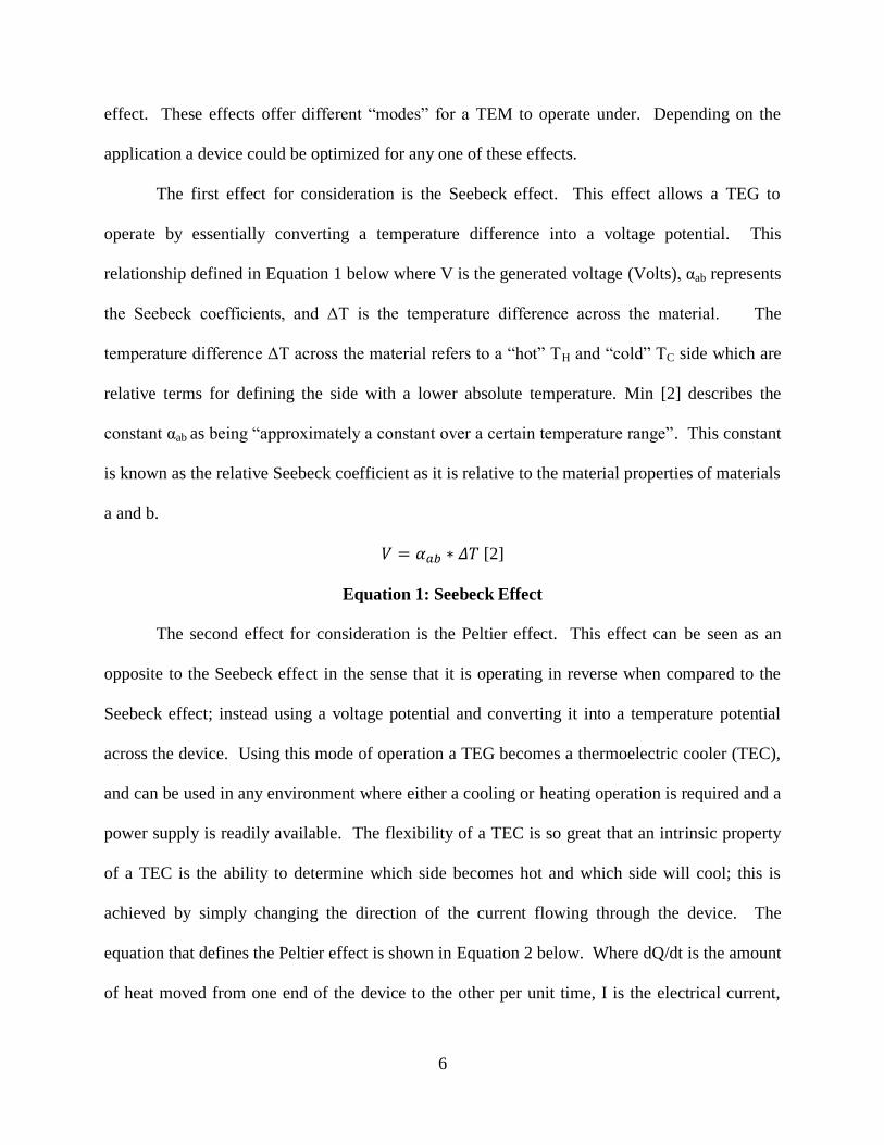
The first effect for consideration is the Seebeck effect. This effect allows a TEG to
operate by essentially converting a temperature difference into a voltage potential. This
relationship defined in Equation 1 below where V is the generated voltage (Volts), αab represents
the Seebeck coefficients, and ΔT is the temperature difference across the material. The
temperature difference ΔT across the material refers to a “hot” TH and “cold” TC side which are
relative terms for defining the side with a lower absolute temperature. Min [2] describes the
constant αab as being “approximately a constant over a certain temperature range”. This constant
is known as the relative Seebeck coefficient as it is relative to the material properties of materials
a and b.
[2]
Equation 1: Seebeck Effect
The second effect for consideration is the Peltier effect. This effect can be seen as an
opposite to the Seebeck effect in the sense that it is operating in reverse when compared to the
Seebeck effect; instead using a voltage potential and converting it into a temperature potential
across the device. Using this mode of operation a TEG becomes a thermoelectric cooler (TEC),
and can be used in any environment where either a cooling or heating operation is required and a
power supply is readily available. The flexibility of a TEC is so great that an intrinsic property
of a TEC is the ability to determine which side becomes hot and which side will cool; this is
achieved by simply changing the direction of the current flowing through the device. The
equation that defines the Peltier effect is shown in Equation 2 below. Where dQ/dt is the amount
of heat moved from one end of the device to the other per unit time, I is the electrical current,

7
and πab is the Peltier coefficient. The Peltier coefficient is similar to the Seebeck coefficient in
the sense that it owes its values to the material properties of the materials being used. Figure 5 is
a graph showing how the Peltier coefficients of P and N type silicon vary with temperature.
Fahrner et al. [1] relate the Seebeck coefficient and Peltier coefficient at a given temperature T
by Equation 3 below. This is one of the Kelvin relationships that relate the different
thermoelectric effects together. Figure 6 is a schematic comparison of the Peltier effect (A) and
the Seebeck effect (B). Both “legs” of the thermoelectric element are connected by a conductor
at the top so that multiple elements would be connected in series.
Equation 2: Peltier Effect [2]
Equation 3: Relation of Peltier and Seebeck coefficients [2]
Figure 5: Peltier coefficient for P and N type Si [1]

8
Figure 6: Comparison of Peltier and Seebeck effects [1]
The third effect for consideration is the Thomson Effect. By contrast the Seebeck and
Peltier effects require the presence of two different materials in order to work. The Thomson
effect is the phenomenon that occurs when a material is subjected to both a temperature potential
and an electrical current producing a heat flux in or out of the material. This effect is illustrated
in Figure 7 below. Min [2] explains that this mode is not considered unless the temperature
difference across a thermoelectric is large; and no device would be designed to operate in a
“Thomson” mode alone. Despite not being accounted for in most thermoelectric designs, the
Thomson effect is present in every thermoelectric conversion. The equation to define the
Thomson effect is given in Equation 4. Similar to the Seebeck and Peltier effects the Thomson
effect has an associated coefficient β. The second Kelvin relationship that relates the Thomson
effect, Seebeck effect, and Peltier effect is shown in Equation 5. Notice the presence of two β
coefficients one for each material present. Each constant can be measured under isothermal
conditions.

9
Figure 7: The Thomson effect [2]
Equation 4: Thomson effect [2]
Equation 5: Second Kelvin relationship [2]
Design
Typically a TEM contains multiple pairs of n and p type thermo-elements arranged so
that they can be connected electrically in series. While the topography of the device can vary
depending on the application individually a single pair of thermo-elements will not generate
sufficient voltage to be of use. By wiring pairs in series enough voltage can be generated to
operate a useful device. Conductors can be of varying materials, depending on the application
and the intended manufacturing process. For example when making a micro scale device it
10
could be prudent to use gold for the conductors due to the need for strong acids in the fabrication
process.
TEMs need to also be packaged in such a way that they remain thermally conductive and
that they fit the environment they are being placed in. For use in biomedical applications for
example the packaging would have to be nontoxic and be able to function at body temperature.
For many commercial applications the TEM is typically packaged between two thermally
conductive substrates of a scalable thickness and overall dimension. The substrates are made of
thermally conductive ceramic, silicon or glass for micro scale applications, or thin polymer
substrate membranes for biomedical applications. Packaging should also not short circuit the
device, if using an electrically conductive substrate care must be taken to isolate the individual
thermoelectric elements. It is not uncommon that the substrates are adhered on either side with
some type of thermal grease to ensure even heat distribution and good contact between the
substrate surfaces.
The topography for a device should be chosen depending on the intended use. The
typical topography for use in a TEM is the monolithic style [3]. By using the monolithic style a
temperature gradient can be established across the device and both substrates have large areas of
contact available. This pattern also allows for a wide range of deposition methods for the
thermoelectric materials. Lastly the monolithic topography is scalable from the macro down to
the nano-scale and benefits from the rapid change in aspect ratio that occurs when scaling down.
Figure 8 is a diagram of the monolithic topography.
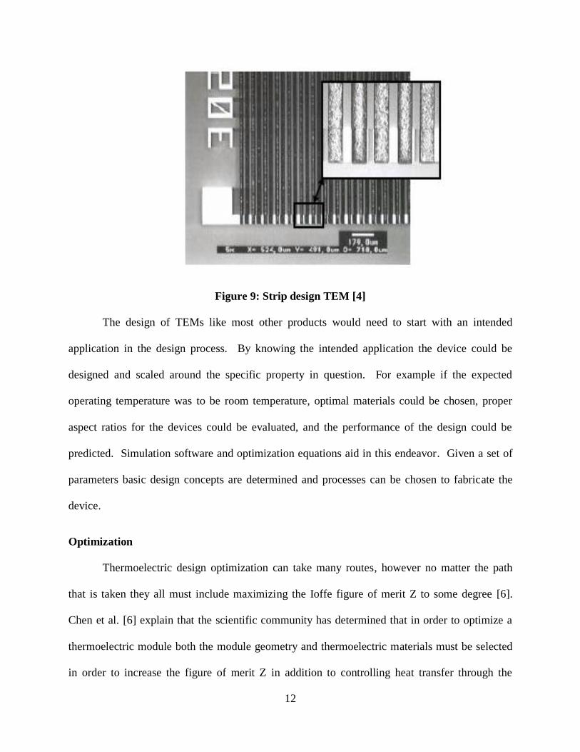
Other topographies include a “strip” design that takes the traditional monolithic
thermoelectric element and lays it on its side. The “strips” are deposited in an alternating n and p
type pattern via a sputtering PVD system that allows multiple targets to be used in order to
11
combine the thermoelectric materials together [4]. The strips are then wired in series by sets of
contacts on either end of the strips. This topography may be desired for thin film designs or
where the overall thickness of the device is critical. The fabrication process is also less
complicated than the traditional monolith style. However this design suffers from increased
joule heating and resistance from the long lengths of thermoelectric material with a thin cross
sectional area. A strip design is shown in Figure 9 below.
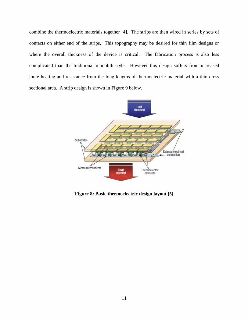
Figure 8: Basic thermoelectric design layout [5]
12
Figure 9: Strip design TEM [4]
The design of TEMs like most other products would need to start with an intended
application in the design process. By knowing the intended application the device could be
designed and scaled around the specific property in question. For example if the expected
operating temperature was to be room temperature, optimal materials could be chosen, proper
aspect ratios for the devices could be evaluated, and the performance of the design could be
predicted. Simulation software and optimization equations aid in this endeavor. Given a set of
parameters basic design concepts are determined and processes can be chosen to fabricate the
device.
Optimization
Thermoelectric design optimization can take many routes, however no matter the path
that is taken they all must include maximizing the Ioffe figure of merit Z to some degree [6].
Chen et al. [6] explain that the scientific community has determined that in order to optimize a
thermoelectric module both the module geometry and thermoelectric materials must be selected
in order to increase the figure of merit Z in addition to controlling heat transfer through the

13
device. Equation 6 and Equation 7 below define the thermoelectric figure of merit for the
thermoelectric material and module respectively. The Seebeck coefficient α is the largest factor
to contributing to a higher figure of merit, ρ is the electric resistivity, while R is the internal
resistance of the system; k represents the thermal conductivity and K is the conductance of the
system. These equations show that in order to have a successful device a material should have
the highest Seebeck coefficient possible while minimizing resistance and thermal conductivity
[7]. Minimizing thermal conductivity may seem counter intuitive for a material designed to cool
or heat a targeted area, but with increasing thermal conductivity the thermoelectric materials
would become uniform in temperature thus inhibiting their ability to produce a usable
temperature gradient necessary for heat transfer. This could be exploited by a designer who
would like to create some sort of “thermal switch” that would have the thermoelectric module
“switch off” at a given temperature. A thermal switch could be used as a sensor device that can
be activated when the given region becomes too hot or cold thus inhibiting the flow of electric
current through the device.
Equation 6: Figure of merit for thermoelectric material [6]
Equation 7: Figure of merit for thermoelectric module [6]
Several assumptions are made when determining performance parameters for a TEM.
The device is considered adiabatic to the environment with the exception of the two thermally
conductive substrates and contact impedance is ignored for simplicity [6]. With these basic
conditions met optimization of individual parameters can be investigated. Figure 10 is a
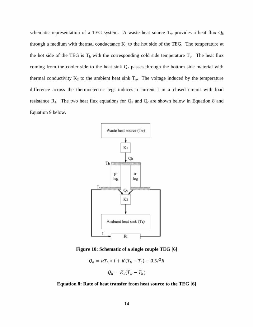
14
schematic representation of a TEG system. A waste heat source Tw provides a heat flux Qh
through a medium with thermal conductance K1 to the hot side of the TEG. The temperature at
the hot side of the TEG is Th with the corresponding cold side temperature Tc. The heat flux
coming from the cooler side to the heat sink Qc passes through the bottom side material with
thermal conductivity K2 to the ambient heat sink Ta. The voltage induced by the temperature
difference across the thermoelectric legs induces a current I in a closed circuit with load
resistance R1. The two heat flux equations for Qh and Qc are shown below in Equation 8 and
Equation 9 below.
Figure 10: Schematic of a single couple TEG [6]
( )
( )
Equation 8: Rate of heat transfer from heat source to the TEG [6]

15
( )
( )
Equation 9: Rate of heat transfer from cold junction to heat sink [6]
Equation 10 below details the total internal resistance for a TEG using a thermoelectric-
coupled model. This model takes into account both internal and external irreversible heat
transfer where ρp and ρn are the electrical resistivity’s of the p and n type material respectively; L
is the length of the thermoelectric elements which for the n and p type legs are assumed to be
equal, and the cross-sectional area of the p and n-type legs are Sp and Sn respectively [6]. This
equation accounts for much of the losses in a TEG device and would require significant
consideration to the element leg lengths and cross sectional areal with respect to the resistivity of
the material. The thermal conductance of a of the module K is summarized in Equation 11
below and with the variables defined above in addition to the thermal conductivity of the p and
n-type materials kp and kn.
(
)
Equation 10: Total internal resistance [6]
(
)
Equation 11: Thermal conductance of a TEG couple [6]
Calculating the output current from a TEG requires a close circuit analysis with a load
with a given load resistance R1. The Seebeck coefficient for the module α is equal to the
difference of the p-type Seebeck coefficient αp and the n-type Seebeck coefficient αn for the
semiconductor materials. The output current is summarized in Equation 12 below for a given
temperature difference ΔT. The output voltage from the TEG is defined in Equation 13 below as

16
Vout. The output power is defined in Equation 14 below. Lastly the power conversion efficiency
which is a ratio to the power generated to the input heat Qh and is shown in Equation 15 below.
Equation 12: Electrical current generated under load [6]
Equation 13: Output Voltage for a TEG [6]
( )
Equation 14: Power output for a TEG [6]
Equation 15: Power conversion efficiency for a TEG [6]
The equations for TECs differ in from their generator counterparts. Equation 16 and
Equation 17 describe how to calculate the coefficient of performance (COP) and the optimum
COP. These equations hold promise for a TEC because a COP of greater than one can be
achieved for relatively small ΔT values of less than 30K [8]. The COP value is a ratio of the
energy supplied to the load and the amount of heat energy adsorbed at the hot junction [9]. In
addition to knowing the optimum COP values, the current at which the COP values are
maximized is given by Equation 18.
Equation 16: Coefficient of Performance [8]

17
√
( √ )
Equation 17: Optimum COP[8]
(√ )
Equation 18: Optimum Current [8]
The aspect ratio of the individual thermoelectric elements is an important parameter to
consider and is the primary advantage of miniaturization for TEMs. The aspect ratio γ is defined
as the thermoelectric geometry area to length ratio and uses the macro scale unit meter(m) [8].
Taylor indicates that at an aspect ratio of 0.001 m at a ΔT of 30K will produce a COP of greater
than 1 [8]. The final optimization equation for consideration would be for the aspect ratio shown
in Equation 19 below. A temperature of 50 C is used for Tc and a current of 1 A is assumed;
from this a parabolic relation is formed and a maximum value can be derived[8]. Optimization
of a TEM can be achieved by using these equations in conjunction with a set of design
parameters in mind. Other optimization equations exist for different topographies and fabrication
methods. Xuan and Wartanonicz discuss how to optimally design a multistage TEM and provide
detailed equations on how to maximize performance while minimizing cost [10, 11].
(√ )
Equation 19: Optimum Aspect ratio [6]
18
Thermoelectric materials processing
Fabrication of microscale TEMs has taken advantage of recent advances in fabrication
technologies particularly in the field of high aspect ratio fabrication and electrochemical
technologies for thin film applications. Scaling of TEMs by means of new fabrication methods
increases overall performance of the devices and lowers costs. The performance increase comes
from increasing the specific power (W/cm2) of the device while maintaining a favorable aspect
ratio [12]. TEMs have the advantage of being very flexible with respect to design considerations
and having no moving parts enables for the selection of a wide selection of manufacturing
processes. Using optimization equations and basic design principles specific processes can
identified for use in fabrication of a TEM.
After selecting an application that the TEM will operate in, material selections are made
to fit the application. Biomedical applications for example would likely use a biocompatible
polymer for a substrate while higher temperature applications could use a silicon or glass
substrate. Surfaces that allow for strong adhesion for metals are highly desirable for a TEM due
to the relatively large and high aspect features that are built on to the surfaces. Substrate
selection should also allow for desirable heat transfer properties to allow for desirable
temperatures on either ends of the device. Lin et al. [12] fabricated a working TEM using glass
slides and discussed using oxidized silicon as a suitable substrate. Oxidized Si wafers can also
be used to create a TEM using traditional N and P well transistor technology.
Metallization of substrates and subsequent components of the TEM can be done by a
wide variety of methods. To create working bottom electrodes thin film deposition processes are
used and are a requirement for miniaturization. Typically monolith type topographies will have
19
interconnecting bridges that are deposited by an electrochemical bath and must be thick enough
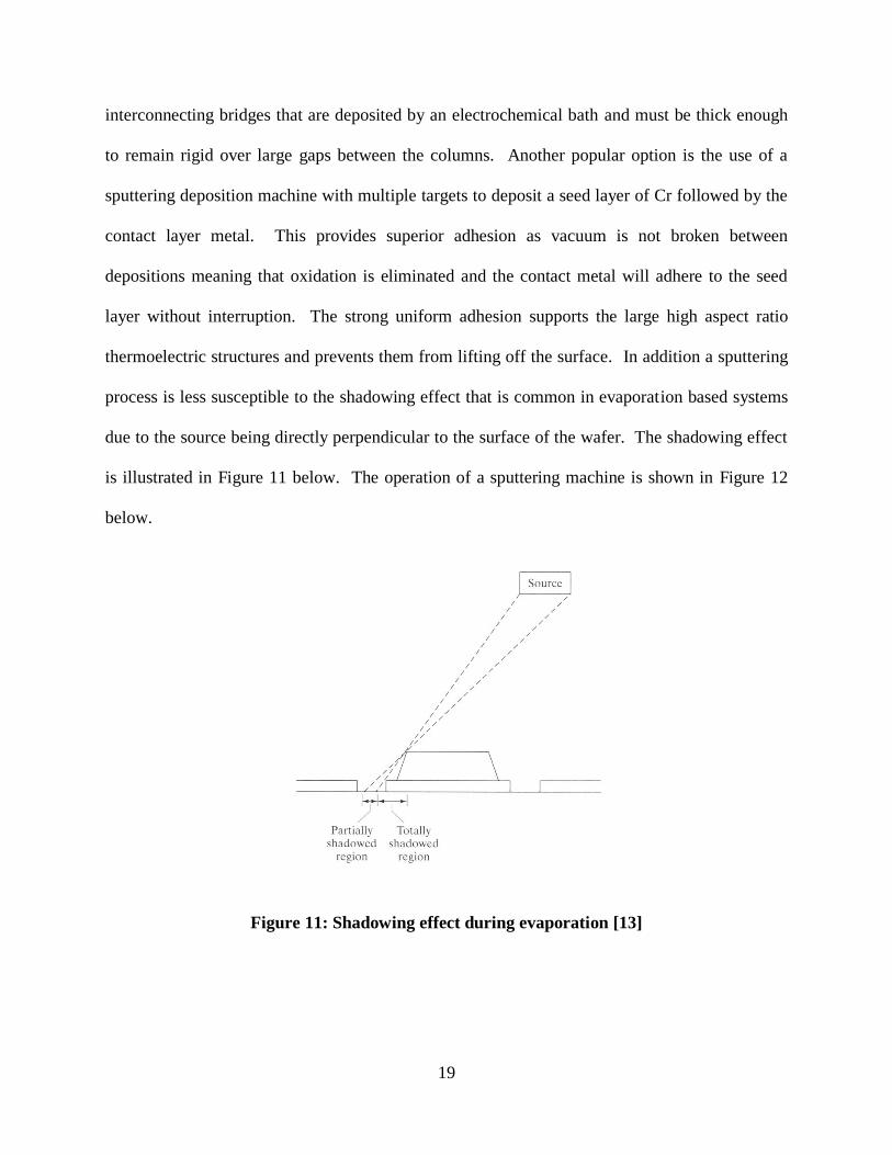
to remain rigid over large gaps between the columns. Another popular option is the use of a
sputtering deposition machine with multiple targets to deposit a seed layer of Cr followed by the
contact layer metal. This provides superior adhesion as vacuum is not broken between
depositions meaning that oxidation is eliminated and the contact metal will adhere to the seed
layer without interruption. The strong uniform adhesion supports the large high aspect ratio
thermoelectric structures and prevents them from lifting off the surface. In addition a sputtering
process is less susceptible to the shadowing effect that is common in evaporation based systems
due to the source being directly perpendicular to the surface of the wafer. The shadowing effect
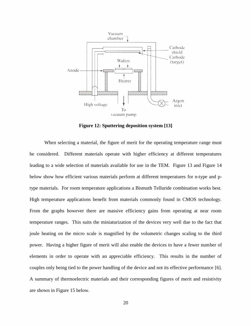
is illustrated in Figure 11 below. The operation of a sputtering machine is shown in Figure 12
below.
Figure 11: Shadowing effect during evaporation [13]
20
Figure 12: Sputtering deposition system [13]
When selecting a material, the figure of merit for the operating temperature range must
be considered. Different materials operate with higher efficiency at different temperatures
leading to a wide selection of materials available for use in the TEM. Figure 13 and Figure 14
below show how efficient various materials perform at different temperatures for n-type and p-
type materials. For room temperature applications a Bismuth Telluride combination works best.
High temperature applications benefit from materials commonly found in CMOS technology.
From the graphs however there are massive efficiency gains from operating at near room
temperature ranges. This suits the miniaturization of the devices very well due to the fact that
joule heating on the micro scale is magnified by the volumetric changes scaling to the third
power. Having a higher figure of merit will also enable the devices to have a fewer number of
elements in order to operate with an appreciable efficiency. This results in the number of
couples only being tied to the power handling of the device and not its effective performance [6].
A summary of thermoelectric materials and their corresponding figures of merit and resistivity
are shown in Figure 15 below.
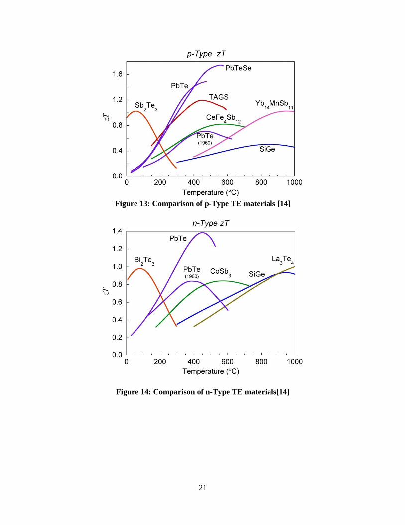
21
Figure 13: Comparison of p-Type TE materials [14]
Figure 14: Comparison of n-Type TE materials[14]
22
Figure 15: Summary of thermoelectric material properties [15]
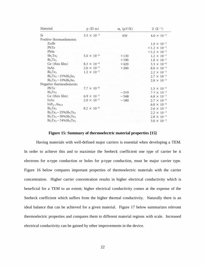
Having materials with well-defined major carriers is essential when developing a TEM.
In order to achieve this and to maximize the Seebeck coefficient one type of carrier be it
electrons for n-type conduction or holes for p-type conduction, must be major carrier type.
Figure 16 below compares important properties of thermoelectric materials with the carrier
concentration. Higher carrier concentration results in higher electrical conductivity which is
beneficial for a TEM to an extent; higher electrical conductivity comes at the expense of the
Seebeck coefficient which suffers from the higher thermal conductivity. Naturally there is an
ideal balance that can be achieved for a given material. Figure 17 below summarizes relevant
thermoelectric properties and compares them to different material regions with scale. Increased
electrical conductivity can be gained by other improvements in the device.
23
Figure 16: Dependency of thermoelectric properties based on carrier concentration [9]
Figure 17: Summary of thermoelectric properties [14]

24
Electrochemical deposition is a favored deposition method for thermoelectric materials
due to the relative low cost and complexity of the technology. Electrochemical deposition
allows for both N and P type thermoelectric materials to be deposited in thin films into molds
created by photolithography or other techniques. For a TEM device typically positive
photoresist is used due to the favorable image width to thickness ratio [16]. Electrochemical
deposition of the thermoelectric materials is done with strong electrolytes; typically strong acids
of at least 65% concentration are used. Nitric acid diluted with deionized to make a 1 M solution
with a pH of 0 offers a flexible electrolyte that allows for good dissolution of the thermoelectric
materials [17]. Figure 18 below shows the deposition and stripping voltages for bismuth
telluride of a concentration of 8.2 mM Bi and 10.3 mM Te in 1M HNO3. With low potentials
thermoelectric material can be bonded to the surface of many common metals including nickel,
copper, stainless steel, and gold making it a cost effective way to form thermoelectric elements.
Figure 18: Cyclic voltammogram for deposition and stripping for optimized bismuth
telluride 8.2 mM Bi, 10.3 mM Te in 1 M HNO3 [17]
25
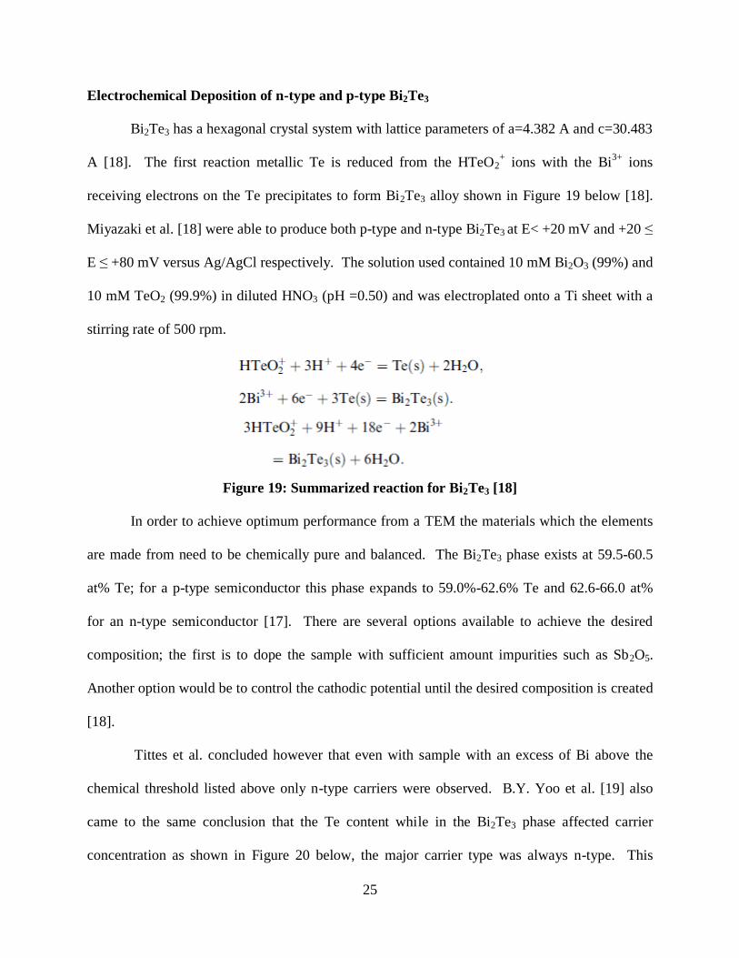
Electrochemical Deposition of n-type and p-type Bi2Te3
Bi2Te3 has a hexagonal crystal system with lattice parameters of a=4.382 A and c=30.483
A [18]. The first reaction metallic Te is reduced from the HTeO2+ ions with the Bi
3+ ions
receiving electrons on the Te precipitates to form Bi2Te3 alloy shown in Figure 19 below [18].
Miyazaki et al. [18] were able to produce both p-type and n-type Bi2Te3 at E< +20 mV and +20 ≤
E ≤ +80 mV versus Ag/AgCl respectively. The solution used contained 10 mM Bi2O3 (99%) and
10 mM TeO2 (99.9%) in diluted HNO3 (pH =0.50) and was electroplated onto a Ti sheet with a
stirring rate of 500 rpm.
Figure 19: Summarized reaction for Bi2Te3 [18]
In order to achieve optimum performance from a TEM the materials which the elements
are made from need to be chemically pure and balanced. The Bi2Te3 phase exists at 59.5-60.5
at% Te; for a p-type semiconductor this phase expands to 59.0%-62.6% Te and 62.6-66.0 at%
for an n-type semiconductor [17]. There are several options available to achieve the desired
composition; the first is to dope the sample with sufficient amount impurities such as Sb2O5.
Another option would be to control the cathodic potential until the desired composition is created
[18].
Tittes et al. concluded however that even with sample with an excess of Bi above the
chemical threshold listed above only n-type carriers were observed. B.Y. Yoo et al. [19] also
came to the same conclusion that the Te content while in the Bi2Te3 phase affected carrier
concentration as shown in Figure 20 below, the major carrier type was always n-type. This

26
allows for a wider window of flexibility when electrochemically depositing Bi2Te3. The point of
contention from the scientific community seems to be the question of whether or not producing
p-type Bi2Te3 is possible or not. B.Y. Yoo et al. [19] postulates that previous research performed
by Magri et al. [20] that demonstrated a linear relationship between film composition and carrier
concentration which does not match other scientific results was caused by differences in BixTey
composition. Magri et al. studied film composition from a range of 63.6 at. % Te (Bi1.8Te3.2) to
70.0 at. % Te (Bi1.5Te3.5) which is well into the Te rich phase meaning that the microstructure
would vary significantly [19]. So based on this it can be concluded that using a single chemical
bath but altering the deposition potentials both an n-type and p-type BixTey. Figure 21 below
illustrates how the major carrier type of a Bi2Te3 compound is affected by the amount of Te
present.
Figure 20: Carrier concentration as a function of Te Content[19]

27
Figure 21: Major carrier type as a function of at. % Te [15]
Variables to control the stoichiometry of the thermoelectric material include the amount
of precursors in the electrolyte, current density applied, duty cycle if applicable, and stirring rate.
The amount of precursors in the electrolyte typically range from 1mM to 10 mM amounts, to
obtain Bi2Te3 a ratio of 3:3-4:3 is used [17, 21]. Current densities vary depending on the type of
electrical signal used; AC signals with a low duty cycle ~2-4% require an average current density
between 5 mA/cm2 and 20 mA/cm
2. DC signals with a full forward duty cycle would have
current densities between 2 mA/cm2
and 5 mA/cm2 [17]. The last major variable to consider
would be the stirring rate of the electrolyte by magnetic stirrer. Stirring can affect the both the
mechanical and chemical properties of the deposited thermoelectric film. For Bi2Te3, the amount
of Te can vary wildly due to the stirring in the electrolyte. Figure 22 below shows the effects of
stirring on the current density for a solution containing Bi2Te3 precursors. Stirring causes an
effect where the effective current density increases due to an increase in the diffusion rate of ions
in the solutions. From observations of experimental data a higher current density typically
correlates to a lower Te content however Soilman et al. observed that although the current
density increased with stirring the content of Te actually increased with the effective current

28
density [22]. Soilman et al. [22] postulate that a similar effect observed from the interelectrode
distance and attributes it a change in flow conditions and a change in oxygen levels on the
surface of the samples.
Figure 22: Voltammogram comparing a solution with and without stirring [22]
Electrochemical Deposition of p-type Bi2-xSbxTe3
The ternary alloy Bi2-xSbxTe3 is a more challenging material to deposit with
electrochemical deposition than its binary counterpart. Bi2-xSbxTe3 electroplates at a much lower
average current density leading to a slow growing film; in addition there are extra processing
steps and additives that much be used. The addition of antimony Sb, adds a host of new
problems in controlling composition and solubility limits for the electrolyte [23]. At room
temperature however Bi2-xSbxTe3 provides the best performance as shown in Figure 13 and
provides a counterpart to the n-type Bi2Te3 for a TEM. For a segmented TEM this p-type
material could be used for the material on the cool side of the device.
The process of forming a Bi-Sb-Te ternary system has a complicated reduction system
that occurs in layers [24]. Li et al. [24] concluded that the TeO2 ion is reduced to Te0 on the

29
surface of the electrode which induces a co-deposition of Bi3+
to form Bi2Te3. The newly
formed Bi2Te3 shifts the polarizing potential negatively to the point of inducing the co-deposition
of Bi3+
and SbIII
with Te0 will form the Bi2-xSbxTe3 [24, 25]. The entire process is summarized
below in Figure 23. The structure of Bi2-xSbxTe3 is also prone to surface roughness
complications due to the crystal structure of Bi2-xSbxTe3 shown in Figure 24 below, and the
substitution of Bi and Sb atoms with Te atoms. Richoux et al. [26] showed how altering the
experimental conditions could affect the stoichiometry of the alloy even if the average current
density remained the same; with an increase in Te content surface roughness ranged from 10nm
to 360 nm for Bi0.38Sb1.43Te3.19 and Bi0.33Sb1.07Te3.6 respectively. Changing the duty cycle also
affected the surface roughness with a higher duty cycle and average current density having a
lower roughness value. Richoux et al. [26] determined that there was an inverse relationship
between roughness values and grain sizes with the rougher surfaces having smaller grain sizes
produced by using a lower duty cycle. This change in grain size is attributed to nucleation of the
grains and the atomic radii of the elements used.
Figure 23: Reduction of Bi-Sb-Te system [24]

30
Figure 24: Bismuth antimony telluride rhombohedral cell [26]

31
CHAPTER THREE: METHODOLOGY
Design of a complete thermoelectric device requires studying of all aspects of production
including composition and fabrication, analytical optimization, processing procedures, and
analyzing the design with finite element analysis. By first studying different types of
thermoelectric thin films further processing designs can be based on the results of the material
study. For example if it is discovered that a particular film process yields a cost savings or a
higher quality film, the fabrication process for a final device can adjust to accommodate the
superior film type. After determining the thermoelectric films that are to be used during
processing analytical models based on known material properties of the fabricated films can be
used to design a device. Lastly the production devices can be analyzed by finite element models
to evaluate expected performance parameters.
Bi2Te3 Fabrication Study
Fabrication of TEMs by electrochemical deposition requires precise control over the
electrolyte and the precursors diluted in the electrolyte. Maintaining control of errant particles
and contaminates in the electrolyte solution is essential to obtaining working solutions of
thermoelectric materials. To obtain a 1M solution of HNO3, 64.10 mL of 65% concentration
HNO3 is slowly poured into 500 mL of deionized water and is then filled to 1000mL with
deionized water in a thoroughly cleaned 1000mL beaker. Next the molar mass of each precursor
is carefully weighed using a Denver Instrument APX-60 scale on weighing paper and added to
the solution; for a solution containing 8.2 mM of Bi2O2 and 10.3 mM of O2Te that would
correlate to 3.821g of Bi2O2 and 1.644g of O2Te. The beaker containing the electrolyte and
precursors is placed into a Fisher Scientific FS60D ultrasonication device for 15 minutes to allow

32
for the particles of precursors to break apart and further dissolve into the electrolyte. After
ultrasonication the solution is placed on a magnetic stirring plate and allowed to stir at 500 rpm
for 24 hours. The solution will be cloudy after stirring and must be filtered prior to use. A
thoroughly cleaned funnel with Fisher Brand P8 filter paper is placed into a second 1000 mL
beaker as shown in Figure 25 below. A glass rod is used to coax the solution into the filtered
funnel slowly.
Figure 25: Filtration of precursors
The samples used for experimentation 0.254mm thick 99.9% pure copper foil that are cut
into 2X1cm sections. The samples are then cleaned in an acetone bath with an ultrasonication
machine for 15 minutes followed by a deionized water rinse with ultrasonication for 5 minutes.
A dilute (1:10) HCL bath with ultrasonication is used for 15 minutes to remove surface oxidation
on the samples. Lastly the samples are rinsed in deionized water with ultrasonication for 5
minutes and are air dried.
A two electrode deposition system is used to deposit the thermoelectric material on the
surface of the sample substrates. An Alfa Aesar 99.9% platinum wire mesh is used as a counter
33
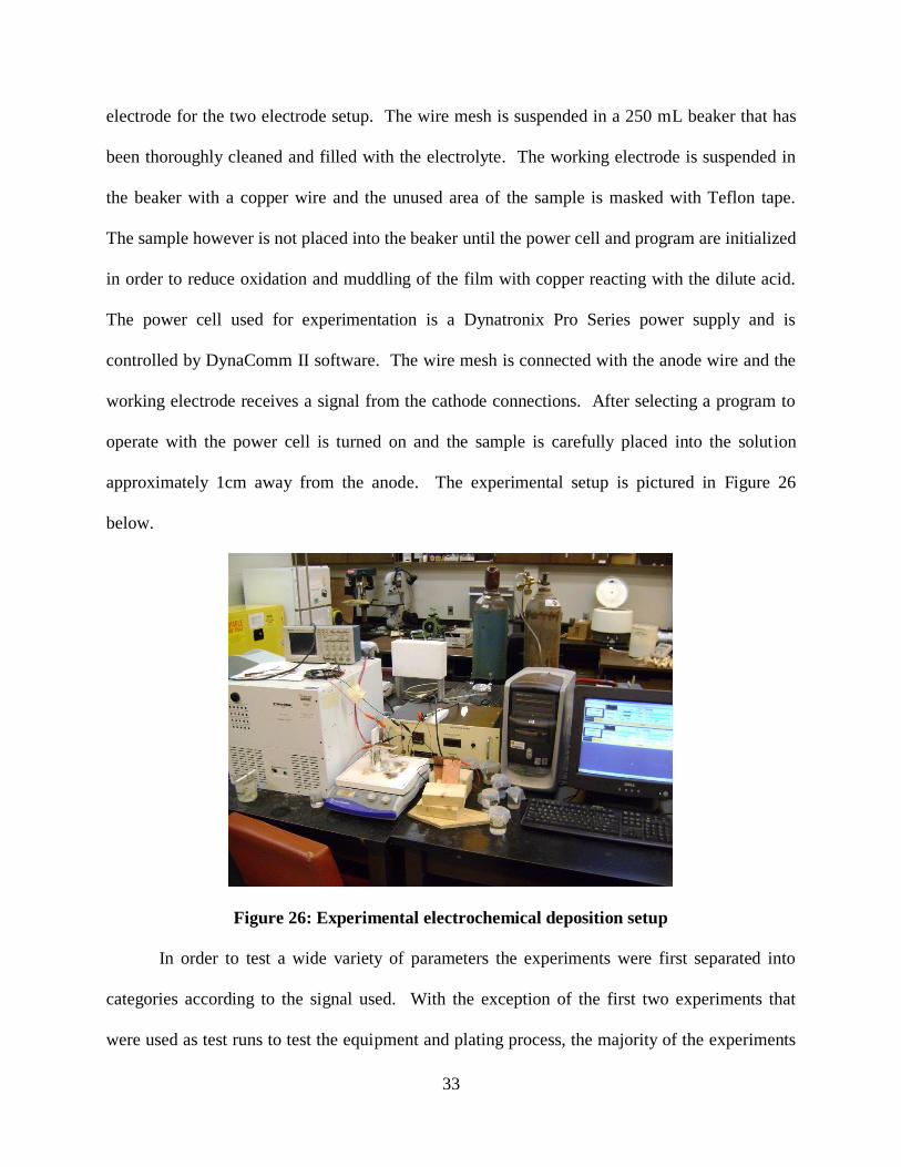
electrode for the two electrode setup. The wire mesh is suspended in a 250 mL beaker that has
been thoroughly cleaned and filled with the electrolyte. The working electrode is suspended in
the beaker with a copper wire and the unused area of the sample is masked with Teflon tape.
The sample however is not placed into the beaker until the power cell and program are initialized
in order to reduce oxidation and muddling of the film with copper reacting with the dilute acid.
The power cell used for experimentation is a Dynatronix Pro Series power supply and is
controlled by DynaComm II software. The wire mesh is connected with the anode wire and the
working electrode receives a signal from the cathode connections. After selecting a program to
operate with the power cell is turned on and the sample is carefully placed into the solution
approximately 1cm away from the anode. The experimental setup is pictured in Figure 26
below.
Figure 26: Experimental electrochemical deposition setup
In order to test a wide variety of parameters the experiments were first separated into
categories according to the signal used. With the exception of the first two experiments that
were used as test runs to test the equipment and plating process, the majority of the experiments

34
were done using pulse plating techniques. A goal of experimentation was to find a solution to
growing n-type materials quickly that had favorable mechanical and electrical properties.
Conventional methods for growing n-type materials use a DC signal however this leads to slow
growth rates thus longer processing times and increased costs; the use of an AC signal with a low
duty cycle is shown to produce materials with the same chemical composition but are grown
faster and with compact structures. The usual results of plating from DC signals were spherical
grains with needle like crystals on the outside. In some cases the alloys produced were uniform
and with few grain boundaries. Table 1 below contains the parameters for the AC signal
experiments and Table 2 contains the parameters for DC signal experiments.
For the AC experiments a wide variety of parameters were changed to experiment with
different pulsing techniques. The power cell used had a minimum allowable peak current as 1
mA. For all experiments the peak voltage was held at 10 V and all samples had an area of 1cm2.
Experiments 1 and two were conducted as test runs and were conducted with a solution that was
far less concentrated than the following experiments. The change in the formula was a result of
observations that the plating was slow and uneven. The higher concentration was used for
further experimentation. Experiments 3 through 5 the peak current was altered to measure the
effects altering the peak current to high levels with a low duty cycle. Experiments 6 through 8
involved altering the duty cycle. Experiments 9 through 11 focused on lower current densities
after examining results from previous experiments. The DC signal experiments were conducted
after running a variety of AC experiments to provide more information about the electroplating
process. The DC signal experiments had fewer variables to contend with since the electroplating
is continuous; experiments 12 through 16 vary the peak current to test a range of average current

35
densities and are summarized Table 2 below. Experiments 17 through 23 were performed to
further test AC signal parameters.
Table 1: AC signal experiments for Bi2Te3, peak voltage 10V, 1cm2
sample
Experiment Peak
Current
(mA)
Avg.
Current
Density
(mA/cm2)
Measured
Voltage
(V)
Measured
Current
(mA)
Time
(min)
Stirring
(rpm)
Duty
cycle
(%)
Composition in
1M HNO3
1(Test run) 263 5 0.09 5 40 60 2 0.8 mM Bi
1mM Te
2(Test run) 40 60 0.8 mM Bi
1 mM Te
3 263 5 0.04 5 40 60 2 8.2 mM Bi
10.3 mM Te
4 500 10 0.05 10 40 60 2 8.2 mM Bi
10.3 mM Te
5 750 15 0.06 14 40 60 2 8.2 mM Bi
10.3 mM Te
6 500 50 0.32 50 10 60 10 8.2 mM Bi
10.3 mM Te
7 500 20 0.14 20 40 60 4 8.2 mM Bi
10.3 mM Te
8 250 10 0.12 10 40 60 4 8.2 mM Bi
10.3 mM Te
9 275 5.5 0.05 5 120 60 2 8.2 mM Bi
10.3 mM Te
10 275 5.5 0.05 5 120 60 2 8.2 mM Bi
10.3 mM Te
11 300 6 0.06 6 120 60 2 8.2 mM Bi
10.3 mM Te
17 288 5.76 0.05 6 120 500 2
8.2 mM Bi
10.3 mM Te
18 288 5.76 0.07 6 120 100 2 8.2 mM Bi
10.3 mM Te
19 325 6.5 0.06 6 40 125 2 8.2 mM Bi
10.3 mM Te
20 350 7 0.05 7 40 125 2 8.2 mM Bi
10.3 mM Te
21 250 5 0.07 5 60 125 2 8.2 mM Bi
10.3 mM Te
22 260 5.2 0.05 5 60 125 2 8.2 mM Bi
10.3 mM Te
23 270 5.4 0.06 5 60 125 2 8.2 mM Bi
10.3 mM Te

36
Table 2: DC Signal Experiments for Bi2Te3, peak voltage 10V, 1cm2
sample 500 rpm
Experiment Peak Current
(mA)
Avg. Current
Density
(mA/cm2)
Measured
Voltage
(V)
Measured
Current
(mA)
Duty cycle
(%)
Composition in
1M HNO3
12 5 5 1.77 5 Full 8.2 mM Bi
10.3 mM Te
13 6 6 1.82 6 Full 8.2 mM Bi
10.3 mM Te
14 7 7 1.81 7 Full 8.2 mM Bi
10.3 mM Te
15 8 8 1.85 8 Full 8.2 mM Bi
10.3 mM Te
16 4 4 1.82 4 Full 8.2 mM Bi
10.3 mM Te
Bi2-xSbxTe3 Fabrication Study
Preparing the electrolyte for Bi2-xSbxTe3 is significantly more complex than its n-type
counterpart. The first p-type Bi2-xSbxTe3 electrolyte is prepared by first diluting 64.10 mL of
nitric acid into 500 mL of DI water. Next the precursors are weighed and diluted into the
solution. To obtain the desired solution 1.5 mM (0.699g) of Bi2O2 , 10 mM (1.596g) of O2Te ,
and 6mM (1.749g) Sb2O3. To aid in dissolving Sb2O3, 0.67 M (100.56 g) of tartaric acid
C4H6O6, a chelating agent is used [27]. The tartaric acid when added to the solution formed
large lumps of material that needed to be broken up manually with a plastic rod and heat was
used to fully dissolve the tartaric acid into the solution. The solution is then filtered in a similar
fashion as the n-type solution was to remove excess particles leaving a clear solution.
Initial experiments with electroplating the p-type material were problematic due to poor
adhesion and achieving the desired chemical composition. Several of the researched formulas
and procedures called for using sub mA current densities with continuous deposition and with

37
the equipment available this would have been impossible thus some improvisations were used.
Using pulse plating techniques low current densities could be achieved although the results were
often not favorable. The sub mA current densities led to slow plating and film development.
Often the surfaces would be uneven and large areas would be devoid of any electroplated
material. Improvisations such as using variable electroplating parameters and altering stirring
rates did not yield any significant results. After exhausting options for constant electroplating
with the available equipment pulse electroplating techniques were tested. Using a target current
density of 2.74 mA which is cited by Richoux et al. [26] as an ideal current density for
depositing Bi2-xSbxTe3; even with following the prescribed procedure with precision and
contacting the author for possible improvements to film quality, a usable film was unable to be
produced. This may have been a result of using a copper substrate as opposed to a gold
substrate; the copper substrate was in the form of copper strips and not sputtered in a smooth
layer over a wafer causing increased roughness. The copper strips were also oxidized and had to
be treated prior to use; it is possible that the combination of excessive surface roughness and
residual oxide caused the poor adhesion. Several publications indicated similar problems with
film purity and adhesion; likely causes included excessive contaminates in the film. It is for
these reasons that Bi2-xSbxTe3 was not chosen as the p-type material and instead a p-type version
of Bi2Te3 would be selected for the relative simplicity in manufacturing useable thin films. The
experiments for Bi2-xSbxTe3 characterization are summarized in Table 3 below. Note that two
solutions were mixed denoted as Solution A from Wijesooriyage [27] and Solution B from
Richoux et al. [26].
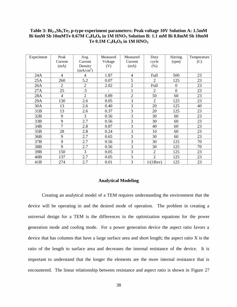
38
Table 3: Bi2-xSbxTe3 p-type experiment parameters: Peak voltage 10V Solution A: 1.5mM
Bi 6mM Sb 10mMTe 0.67M C4H4O6 in 1M HNO3 Solution B: 1.1 mM Bi 8.8mM Sb 10mM
Te 0.1M C4H4O6 in 1M HNO3
Experiment Peak
Current
(mA)
Avg.
Current
Density
(mA/cm2)
Measured
Voltage
(V)
Measured
Current
(mA)
Duty
cycle
(%)
Stirring
(rpm)
Temperature
(C)
24A 4 4 1.87 4 Full 500 23
25A 260 5.2 0.07 5 2 125 23
26A 2 2 2.02 2 Full 0 23
27A 25 .5 - 1 2 0 23
28A 4 2 0.89 2 50 60 23
29A 130 2.6 0.05 3 2 125 23
30A 13 2.6 0.40 3 20 125 40
31B 13 2.6 0.37 3 20 125 23
32B 9 3 0.56 3 30 60 23
33B 9 2.7 0.56 3 30 60 23
34B 7 2.8 0.87 3 40 60 23
35B 28 2.8 0.24 3 10 60 23
36B 9 2.7 0.65 3 30 60 23
37B 9 2.7 0.56 3 30 125 70
38B 9 2.7 0.56 3 30 125 70
39B 150 3 0.05 3 2 125 23
40B 137 2.7 0.05 3 2 125 23
41B 274 2.7 0.01 3 1/(1Rev) 125 23
Analytical Modeling
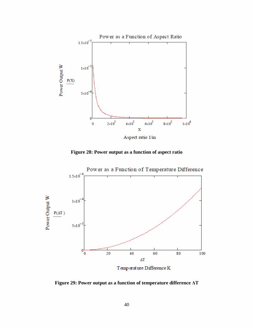
Creating an analytical model of a TEM requires understanding the environment that the
device will be operating in and the desired mode of operation. The problem in creating a
universal design for a TEM is the differences in the optimization equations for the power
generation mode and cooling mode. For a power generation device the aspect ratio favors a
device that has columns that have a large surface area and short length; the aspect ratio X is the
ratio of the length to surface area and decreases the internal resistance of the device. It is
important to understand that the longer the elements are the more internal resistance that is
encountered. The linear relationship between resistance and aspect ratio is shown in Figure 27
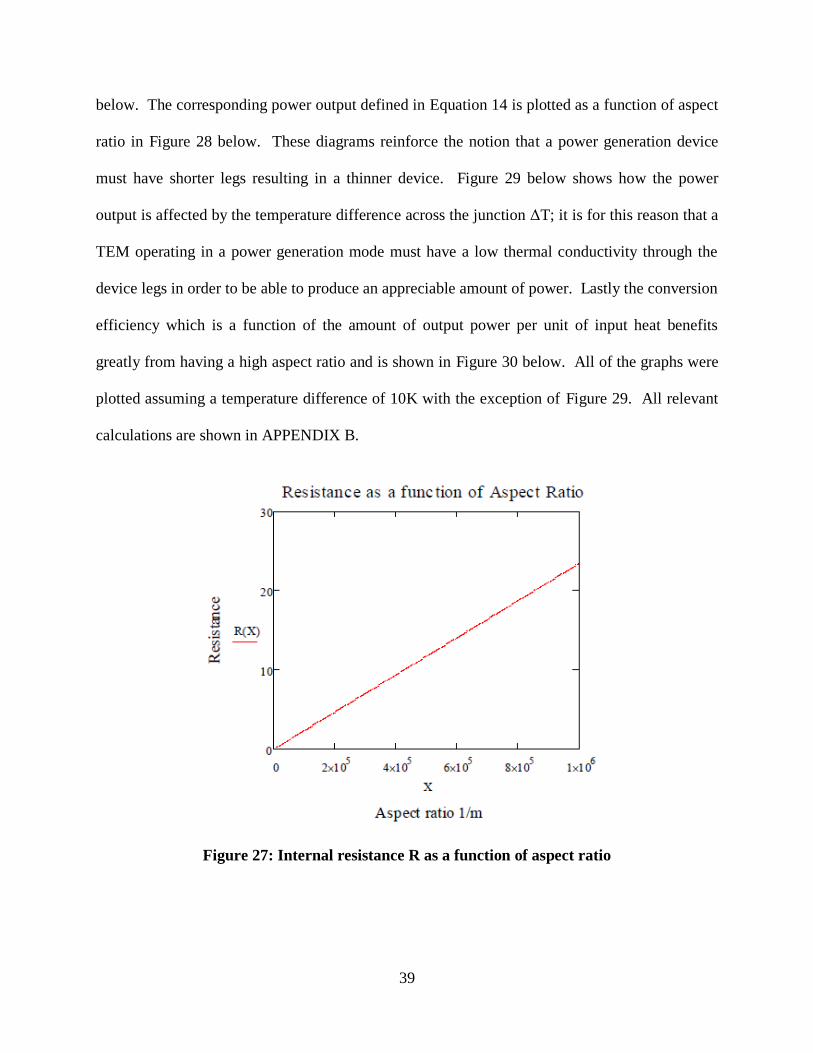
39
below. The corresponding power output defined in Equation 14 is plotted as a function of aspect
ratio in Figure 28 below. These diagrams reinforce the notion that a power generation device
must have shorter legs resulting in a thinner device. Figure 29 below shows how the power
output is affected by the temperature difference across the junction ΔT; it is for this reason that a
TEM operating in a power generation mode must have a low thermal conductivity through the
device legs in order to be able to produce an appreciable amount of power. Lastly the conversion
efficiency which is a function of the amount of output power per unit of input heat benefits
greatly from having a high aspect ratio and is shown in Figure 30 below. All of the graphs were
plotted assuming a temperature difference of 10K with the exception of Figure 29. All relevant
calculations are shown in APPENDIX B.
Figure 27: Internal resistance R as a function of aspect ratio
40
Figure 28: Power output as a function of aspect ratio
Figure 29: Power output as a function of temperature difference ΔT

41
Figure 30: Conversion efficiency as a function of aspect ratio X
Testing device design
In order to fabricate a working device a large collection of design ideas were
implemented into a single feasible TEM fabrication method. A monolithic topography was
determined to provide the best device for testing purposes as it is easily scalable and has been
benchmarked by other research.
The testing mask and device were designed to be easy to dice and manipulate on the bulk
level while providing useful scalable information. The mask design is also in the dark field
configuration for the positive photoresist processing. Another constraint for making the test
device was using a diced wafer rather than a whole three inch wafer. This decision was made to
save money on sputtering runs but added another level of complexity to the device due to the
mask aligner being used. In addition to complicating the use of the mask aligner, large Si

42
particles would be created by dicing the wafer; particle mitigation can be done by coating the
wafer with photoresist prior to dicing in order to “catch” many of the particles being created. Si
particles are notoriously difficult to remove from a wafer due to their ability to adhere to the
smooth Si wafer surface. An individual device on the wafer is 0.5 cm by 0.5 cm. with a total of
9 devices being made per wafer quarter leaving room for dicing lanes and alignment marks. The
mask was designed using AutoCAD 2010; due to the mask fabrication machines available on
campus the mask had to be made using “solid” elements in AutoCAD thus limiting the design of
the mask to items composed entirely of rectangles.
The first layer in the mask is a bottom contact layer. Large contact pads are created to
provide testing areas in addition to providing sufficient contact area for wiring the device. An
array of bottom contacts with dimensions of 60 µm by 180 µm are arranged and spaced to make
good use of the available space. The dimensions of the contact pads were designed to allow for
simple processing for the testing device. An array of scaled smaller pads, were arranged below
the larger pads to allow for testing a second aspect ratio on the same device. The contact pads
were connected to the ends of certain rows to test the scaling of using more pairs of thermo
devices. In the current configuration the first row of 24 couples can be tested individually in
addition to testing four rows, seven rows, and then the entire array. The scaled smaller array is
arranged to test the first row and the entire array of three rows. Lastly the fiducial marks are
arranged to provide sufficient alignment information for a dark field mask. The contact layer
mask is shown in Figure 31 below; note that the mask would be inverted for the dark field
design.

43
Figure 31: Contact layer of testing mask pattern
The second mask layer is used to pattern the p-type columns over the contact pads. The
pattern is used to open columns through the thick photoresist and allow for the depositing of the
p-type material into the photoresist molds created. The design allows for scaling depending on
the thickness of the photoresist; for example the each layer of photoresist can be a maximum of
10 µm, so the aspect ratio can be adjusted by layering multiple photoresist layers and then
exposing with this mask pattern. The columns are arranged to be placed at one end of the
contact pads created earlier during processing. The larger columns are 50 µm by 50 µm and the
smaller columns are scaled to fit the corresponding smaller contact pads. Again this format
allows for multiple avenues for testing the effects of the aspect ratio on a single device. The p-
type column mask pattern is shown in Figure 32 below. The n-type column creation pattern is a
similar design but opens columns on the opposite end of the contact pads. The n-type column
mask is shown in Figure 33 below.

44
Figure 32: P-type column testing mask pattern
Figure 33: N-type column testing mask pattern

45
The final pattern to be applied would be a top interconnection pattern that would wire all
of the columns in series. This final pattern connects the tops of the n and p-type columns
together in an efficient manner. Tolerances were built into the pattern to account for alignment
errors. The top interconnects also string together the entire device meaning that the testing of
individual strings of thermocouples is done with the bottom contact pattern. Lastly the top
interconnection pattern will be patterned onto a thin layer of photoresist applied over the
remaining thick layer of photoresist.
Figure 34: Interconnect testing mask pattern
The culmination of these mask designs were printed on to a single mask in order to save
on production cost for the testing device. Each layer was arranged in a three by three pattern
designed to fit on to a quarter of a three inch wafer. A series of windows were made in the mask
to use as macro scale alignment marks while the smaller micro scale alignment marks present in

46
each unit cell; are used for fine adjustment. Note that this mask is dark field and would be
inverted.
Figure 35: Production mask for testing device
Production of the testing device would begin with a three inch <100> Si wafer that is
thoroughly cleaned and dried. The wafer would then be processed through a sputtering machine
to apply a 0.1 μm layer of Cr for adhesion followed by a 0.1 μm seed layer of Cu. Residual
oxide then removed prior to the next process. The bottom contact mask pattern Figure 31 is then

47
patterned on to the substrate surface using 0.6 μm of S1818 photoresist. The device is then
processed again through a sputtering machine in order to add an additional 0.3 μm of Cu to form
the remainder of the contact layer. The layer is then lifted off using a combination of acetone
and ultrasonication leaving a raised contact region and a thinner sacrificial layer of metal to be
removed later in production.
The creation of the columns for the monolithic topography begins with the application of
SPR 220-7 thick positive photoresist in three 10 μm layers for a total of 30 um. This process
would take a significant amount of time for baking processes and would need to be monitored
carefully. Next using the pattern shown in Figure 32 above the columns for the p-type columns
is exposed and developed opening an array of columns to the raised contact pads. Next the p-
type column pattern is filled using electrochemical deposition with p-type thermoelectric
material. Next a thin layer of S1818 photoresist is spun over the device to cover the p-type
columns and is followed by opening the n-type column pattern shown in Figure 33. The n-type
columns are then filled with the n-type material.
The top interconnection pattern creation begins with removing the thin layer of S1818
over the columns and applying another layer of S1818 to pattern the top interconnection pattern
shown in Figure 34. Next a thin Cr adhesion layer is sputtered on to the surface of the columns
followed by a thick aluminum layer to be used as the top interconnection layer. All photoresist is
then removed slowly with developer in order not to remove the top interconnections via lift off.
Lastly the bottom connections are isolated with copper and chrome etches to remove the thin
sacrificial layer in order to isolate the columns and contact pads. The device would then be
cleaned thoroughly with oxygen plasma followed by a 250 C inert gas annealing process in order

48
to strengthen the thermoelectric materials and improve their electrical properties. A device
profile of the testing device is provided in Appendix A.
Production device design
A second optimized device was designed in order to produce a more feasible device for
commercial use. Optimization of a TEM requires that a mode of operation be chosen; so a
device to be used as a localized power source would require a thin cross section while a cooling
device would be optimized with a thicker cross section. The operating temperature is 10K which
is small enough to be used in a wide variety of applications including biomedical and room
temperature waste heat recovery. The optimization study performed earlier in combination with
research of the power requirements of common sensors culminated in a device that was both
practical and innovative. The fabrication process described for production of the testing device
is a common production method for TEMs; the problem with this production method is the
excessive amount of photoresist applications required through the device production process.
The fabrication of the optimized device makes use of some fabrication techniques and material
choices in order to reduce the number of processes required to fabricate the TEM.
The first major change between the testing mask design and the optimized device is that
each layer would have its own its own mask meaning that an entire wafer would be used for
production rather than fragments for testing purposes. The first mask shown in Figure 37 below
is the bottom contact layer of the updated device. Each contact pad is oversized at 35 μm by 35
μm to allow for connections. Rather than having a blanket connection for all of the contacts for
the electrochemical deposition; the contact patterns are instead wired with an array of smaller
interconnections that will be etched away later. Another fabrication improvement would be the

49
deposition of both the n and p-type material from the same electrolyte. Bi2Te3 can be produced
in both carrier types from the same electrolyte by altering the current density of the deposition.
When submerged in the electrolyte the wafer would have two contacts connected to rows of
contact pads which in turn would lead to macro contact pads used to connect the wafer to the
power supply. Using this design both the column types can be deposited without ever having to
remove the wafer from the electrolyte or cover the previous columns with photoresist between
depositions. One of the major advantages to using a thermoelectric device is the scaling ability
that is inherent to the optimization equations. Altering the thermocouple dimensions scales the
device in addition to the number of thermocouples present meaning that unit cells within the
device can be scaled to operate at a predetermined parameter. Using this mask pattern at there
are six 0.5 V unit cells comprised of 256 pairs of thermoelectric thermocouples. These are
subsequently wired later in the processing using the other contact patterns to allow the device to
operate at different voltages effortlessly. Strings can be made in any combinations meaning that
the device can operate as 6 0.5 V cells or as a single 3.0 V cell or anywhere in between adding
another dimension of flexibility to an already versatile design.
Figure 36: Macro view of bottom contact mask
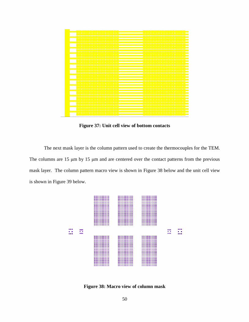
50
Figure 37: Unit cell view of bottom contacts
The next mask layer is the column pattern used to create the thermocouples for the TEM.
The columns are 15 μm by 15 μm and are centered over the contact patterns from the previous
mask layer. The column pattern macro view is shown in Figure 38 below and the unit cell view
is shown in Figure 39 below.
Figure 38: Macro view of column mask

51
Figure 39: Unit cell view of column mask
The next mask is used to sever the connections between the contact pads and is arranged
over the contact layer. The columns need to be isolated as not to short the device during
operation. The long conduits used to connect the rows of contacts to the large contact pads are
also exposed for an etching process. The areas covered by this mask in red are slightly oversized
in order to account for alignment errors and earlier errors during processing. Figure 40 shows
the macro scale view of the isolation mask and Figure 41 shows the unit cell view of the isolation
mask. Notice in Figure 41 the exposure between column contact pads; after use of this mask and
processing only an array of bottom contact pads should remain.

52
Figure 40: Macro view of isolation etch mask
Figure 41: Unit cell view of isolation etch mask
The final mask pattern is the final connection pattern that reconnects the columns in
series on two different levels. In the mask shown below in Figure 42 and Figure 43 below
connections are made at the bottom contacts and at bridging between the top contact pads.
Figure 44 shows how the interconnection pattern creates paths for input and output from each of
the TEM 0.5 V cells.
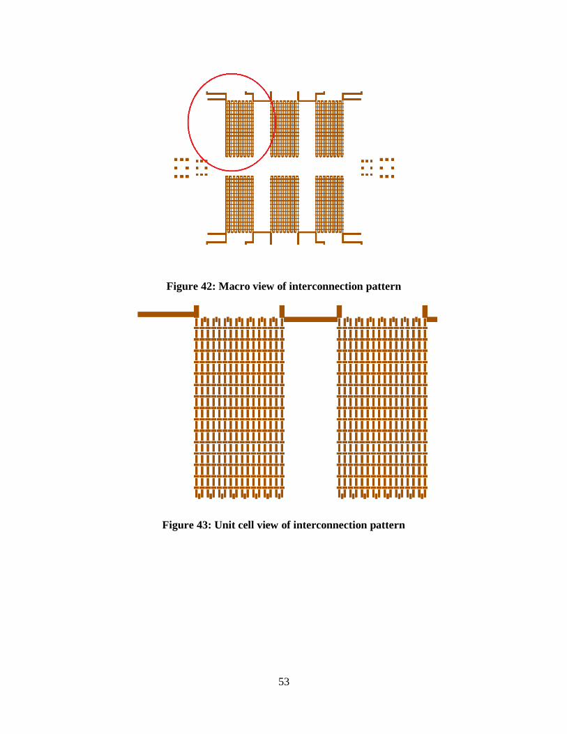
53
Figure 42: Macro view of interconnection pattern
Figure 43: Unit cell view of interconnection pattern

54
Figure 44: Unit cell view interconnection to contact pads
Fabrication of the 10K device would begin with a three inch <100> Si substrate that is
thoroughly cleaned and prepared for photoresist application. A 0.9µm layer of SPR 1818 is
applied over the surface using the pattern from Figure 36 for use in a lift off process. Next the
wafer would be processed by a sputtering machine that would apply an adhesive 0.1 µm layer of
Cr followed by a 0.2µm layer of Cu for use as the bottom contact layer. After sputtering the
wafer would undergo a lift off process removing excess metal leaving behind the bottom contact
layer. Next a 10.0µm layer of SPR-220 positive photoresist is applied using the mask pattern
from Figure 39 to open up the columns for the thermoelectric material to be deposited into.
The electrochemical deposition process would begin by growing a seed layer of the n and
p-type material on the corresponding contacts in order to protect the copper substrate from
excessive exposure to the electrolyte. Next p-type material is grown using the corresponding
contacts to a height of just under 10.0µm to allow room for mushrooming and surface roughness.
The n-type material would then be grown to the same height to produce two legs with roughly
the same profile. The next process would be using the isolation etch mask from Figure 40 to
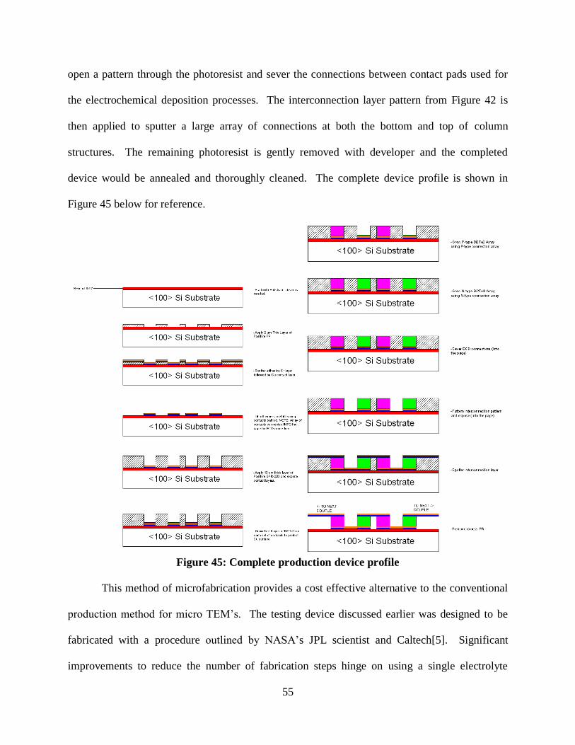
55
open a pattern through the photoresist and sever the connections between contact pads used for
the electrochemical deposition processes. The interconnection layer pattern from Figure 42 is
then applied to sputter a large array of connections at both the bottom and top of column
structures. The remaining photoresist is gently removed with developer and the completed
device would be annealed and thoroughly cleaned. The complete device profile is shown in
Figure 45 below for reference.
Figure 45: Complete production device profile
This method of microfabrication provides a cost effective alternative to the conventional
production method for micro TEM’s. The testing device discussed earlier was designed to be
fabricated with a procedure outlined by NASA’s JPL scientist and Caltech[5]. Significant
improvements to reduce the number of fabrication steps hinge on using a single electrolyte

56
during processing. This eliminates the need to cover the previously deposited columns between
electrochemical depositions. Additionally chemical costs are reduced by the need of only having
to use a single electrolyte bath.
FEA Modeling
Accounting for the large number of variables and challenges that are presented when
fabricating any microelectronic device is a difficult, time consuming, and costly process; with
the advent of modern modeling technologies, thousands of simulations can be calculated before a
single device is fabricated. With TEMs coming to prominence in recent years many traditional
modeling methodologies are being investigated for use in a finite element model of a TEM. A
comprehensive model of a TEM would provide valuable information at a device level and allow
for testing of various configurations and properties without ever having to fabricate a device.
Perhaps the most difficult property to account for with an analytical model would be complex
geometries which can be accounted for with a finite element model. Finite element models can
then be compared to working modules post fabrication.
COMSOL is a powerful multiphysics software package that contains a wide range of
governing equations for a variety of physical phenomena. COMSOL also contains algorithms
for solving nonlinear equations rapidly to convergence [28]. COMSOL allows for specific
subdomains to be drawn in two and three dimensions or imported from another software
package. The subdomains require governing equations be applied and boundary conditions
defined in addition to other predefined variables [29].
Sandoz-Rosado and Stevens [30] developed a robust set of solutions for a TEM system
using the governing equations listed below. Equation 20 represents the vector form of the heat

57
flux on a volume subdomain where T is the absolute temperature, [α] is the Seebeck coefficient
matrix, J is the vector form of the current flux, [k] is the thermal conductivity matrix [30].
Equation 21 defines the electric current density where [σ] is the electrical conductivity matrix
and E is the electric field vector. Equation 22 and Equation 23 define the thermoelectric
subdomains and indicate that current is conserved in steady state conditions [30]. Equation 24
defines the total Joule heating per unit volume. Equation 25 is a combination of Equation 20
through Equation 23; the first term is the bulk Peltier effect and is typically neglected, the second
term is the bulk Thomson heat which is used to vary the Seebeck coefficient depending on the
temperature [30].
[ ] [ ]
Equation 20: Heat Flux [30]
[ ] ( [ ] )
Equation 21: Electric current density [30]
Equation 22: Internal heating [30]
Equation 23: Conservation of Energy [30]
[ ]
Equation 24: Joule heating per unit volume [30]
[ ]
([ ] )
Equation 25: Governing equation for a thermoelectric subdomain [30]
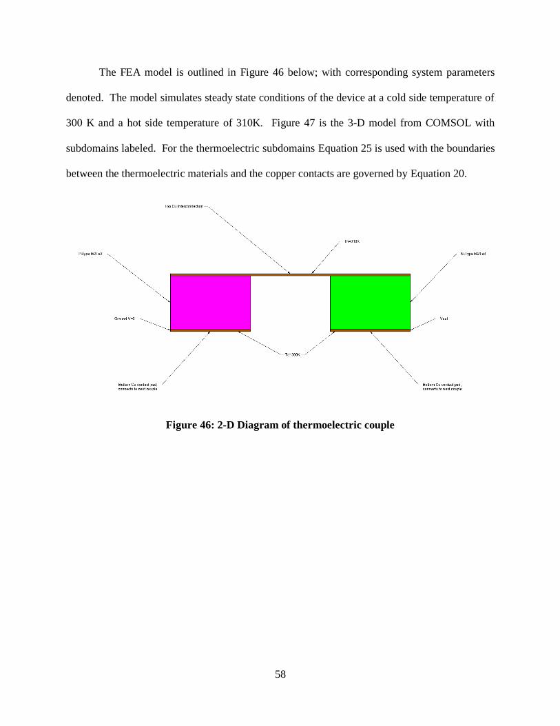
58
The FEA model is outlined in Figure 46 below; with corresponding system parameters
denoted. The model simulates steady state conditions of the device at a cold side temperature of
300 K and a hot side temperature of 310K. Figure 47 is the 3-D model from COMSOL with
subdomains labeled. For the thermoelectric subdomains Equation 25 is used with the boundaries
between the thermoelectric materials and the copper contacts are governed by Equation 20.
Figure 46: 2-D Diagram of thermoelectric couple

59
Figure 47: 3-D Diagram of thermoelectric couple system
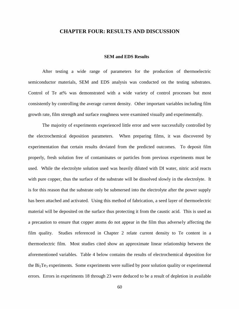
60
CHAPTER FOUR: RESULTS AND DISCUSSION
SEM and EDS Results
After testing a wide range of parameters for the production of thermoelectric
semiconductor materials, SEM and EDS analysis was conducted on the testing substrates.
Control of Te at% was demonstrated with a wide variety of control processes but most
consistently by controlling the average current density. Other important variables including film
growth rate, film strength and surface roughness were examined visually and experimentally.
The majority of experiments experienced little error and were successfully controlled by
the electrochemical deposition parameters. When preparing films, it was discovered by
experimentation that certain results deviated from the predicted outcomes. To deposit film
properly, fresh solution free of contaminates or particles from previous experiments must be
used. While the electrolyte solution used was heavily diluted with DI water, nitric acid reacts
with pure copper, thus the surface of the substrate will be dissolved slowly in the electrolyte. It
is for this reason that the substrate only be submersed into the electrolyte after the power supply
has been attached and activated. Using this method of fabrication, a seed layer of thermoelectric
material will be deposited on the surface thus protecting it from the caustic acid. This is used as
a precaution to ensure that copper atoms do not appear in the film thus adversely affecting the
film quality. Studies referenced in Chapter 2 relate current density to Te content in a
thermoelectric film. Most studies cited show an approximate linear relationship between the
aforementioned variables. Table 4 below contains the results of electrochemical deposition for
the Bi2Te3 experiments. Some experiments were sullied by poor solution quality or experimental
errors. Errors in experiments 18 through 23 were deduced to be a result of depletion in available

61
metal in the electrolyte. The wide range of variables tested resulted in an equally wide variety of
results with several common threads. The first is that with either signal used the current density
that represents the critical point between at the n and p-type transition occurs at a current density
between 4 and 5 mA/cm2. The second is the presence of a linear relationship between the
average current density and the Te content confirming what previous studies have shown. Figure
48 shows the results of experimentation with AC signals and the linear relationship between
current density and Te content. Figure 49 presents the data from the DC experiments and results
in the same conclusion.
Table 4: SEM and EDS results for Bi2Te3 Experiments
Experiment Te at% Te at% error (+/-) Bi at% Bi at %error (+/-) Avg. Current Density
(mA/cm2)
Signal
1 5 AC
2 74.95 +/-11.78 25.05 2.78 AC
3 83.62 3.63 16.37 0.8 5 AC
4 38.7 2.67 61.3 0.96 10 AC
5 24.51 2.63 75.49 1.05 15 AC
6 44.61 3.79 55.39 1.21 50 AC
7 41.13 2.77 58.87 0.94 20 AC
8 22.73 2.66 77.27 1.06 10 AC
9 39.85 2.77 60.15 0.95 5.5 AC
10 55.11 2.68 44.89 0.83 5.5 AC
11 47.2 2.54 52.8 0.85 6 AC
12 63.18 2.21 36.82 0.64 5 DC
13 61.72 2.18 38.28 0.65 6 DC
14 57.93 2.13 42.07 0.66 7 DC
15 55.88 2.49 44.12 0.76 8 DC
16 61.76 2.35 38.24 0.69 4 DC
17 56.72 4.17 43.28 1.23 5.76 AC
18 29.8 2.79 70.2 1.04 5.76 AC
19 41.55 2.34 58.45 0.82 6.5 AC
20 29.05 2.61 70.95 1.01 7 AC
21 36.09 3.09 63.49 0.93 5 AC
22 42.36 2.69 57.64 0.93 5.2 AC
23 38.73 3.12 60.62 0.93 5.4 AC

62
Figure 48: Bi2Te3 composition versus average current density for AC signal experiments
Figure 49: Bi2Te3 composition versus average current density for DC signal experiments
The results summarized in Table 4, Figure 48, and Figure 49 above show that a
relationship exists between the Te content of Bi2Te3 and the average current density during
0
10
20
30
40
50
60
70
4 4.5 5 5.5 6 6.5 7 7.5
Te c
on
ten
t (a
t.%
)
Avg. Current density mA/cm2
55
56
57
58
59
60
61
62
63
64
3 4 5 6 7 8 9
Te c
on
ten
t (a
t.%
)
Avg. Current density mA/cm2

63
deposition. Previous studies have indicated that transition of the major carrier type of the film
can occur when the Te at. % content of the film reaches a critical point of 62.6%.
Inspection of SEM micrographs yields important information concerning film quality and
composition. Experiment 2 shown in Figure 50 shows an extremely thin layer of thermoelectric
film sparsely deposited on the surface of the copper substrate. The detected Te content is from
the targeting of specific areas on the deposited area. Figure 51 is the micrograph of experiment 3
which had an abnormally high amount of Te and can be attributed to the again targeting only a
specific area of the film.
Figure 50: SEM micrograph of Exp. 2
Figure 51: SEM micrograph of Exp. 3

64
Starting at experiment 4 with the testing of higher average current densities massive
changes in film quality can be observed. Bismuth grows in large needle like create a rough
marred surface. Excessive Bi content results in poor film quality with poor adhesion, the film
would easily be damaged by washing the surface. Figure 52 through Figure 56 are the
micrographs of experiments 4 through 8. It can be seen that uniform nucleation does not occur
in these micrographs. The worst instance of this occurred in experiment 6 shown in Figure 54
where the surface roughness left nothing but crystallized Bi on the surface of the substrate.
During processing excessive Bi content could be seen by rapid darkening of the surface rather
than the dull metallic gray color which Bi2Te3 should be.
Figure 52: SEM micrograph of Exp. 4
Figure 53: SEM micrograph of Exp. 5
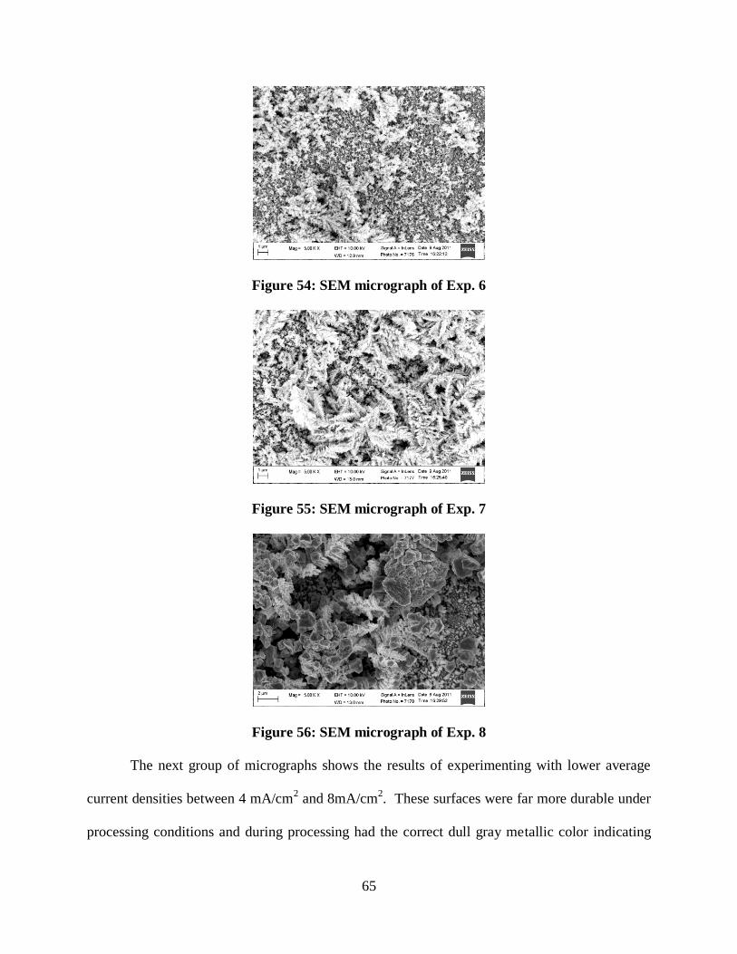
65
Figure 54: SEM micrograph of Exp. 6
Figure 55: SEM micrograph of Exp. 7
Figure 56: SEM micrograph of Exp. 8
The next group of micrographs shows the results of experimenting with lower average
current densities between 4 mA/cm2 and 8mA/cm
2. These surfaces were far more durable under
processing conditions and during processing had the correct dull gray metallic color indicating

66
an improvement in film quality. Looking at the SEM micrographs for experiments 9 and 10
shown in Figure 57 and Figure 58 respectively the results of a depleted electrolyte can be seen.
Both experiments were conducted under the same conditions and at the same potentials; however
in experiment 9 the solution used was several days old and had been used in previous
experiments. Nucleation of the Bi occurred however the lack of Te content resulted in smaller
grains absent Te deposits on their surfaces. Figure 59 was performed at 6 mA/cm2 and had
reduced Te content as expected; note the lack of crystals on the surface on the surface of the
large grains.
Figure 57: SEM micrographs of Exp. 9
Figure 58: SEM micrographs of Exp.10

67
Figure 59: SEM micrographs of Exp. 11
After extensively testing AC parameters more established DC parameters were tested.
Figure 60 illustrates the results of experiment 12; when using a DC signal the morphology of the
Bi2Te3 films changes significantly. Grain sizes are larger and the films are more compact than
the AC signals as seen in Figure 61 though Figure 64 (experiments 13 through 16). Additionally
the surface of the grains changed significantly with the larger surface crystals being replaced by
smaller spine like structures. Experiments 17 through 20 are shown in Figure 65 though Figure
68. Experiments 17 and 18 resulted in films that cracked and peeled from the surface. The
peeling is likely a result of high stress in the film and it was observed that the substrate holder
was at an angle causing some areas of the substrate to be closer to the anode therefore causing
uneven stresses across the film. Experiment 19 produced an interesting result where the film
seemed to homogenize into a single grain with small void zones; in addition the film observed to
be a light grey metallic color which was shiny. Experiment 20 shows the effects of raising the
current density and produced results similar to Experiment 4. Experiments 21, 22, and 23 are not
pictured but the films were of low quality and thus omitted.
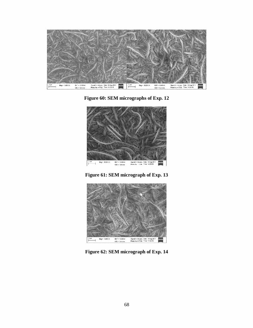
68
Figure 60: SEM micrographs of Exp. 12
Figure 61: SEM micrograph of Exp. 13
Figure 62: SEM micrograph of Exp. 14

69
Figure 63: SEM micrograph of Exp. 15
Figure 64: SEM micrographs of Exp. 16
Figure 65: SEM micrograph of Exp. 17
70
Figure 66: SEM micrograph of Exp. 18
Figure 67: SEM micrographs of Exp. 19
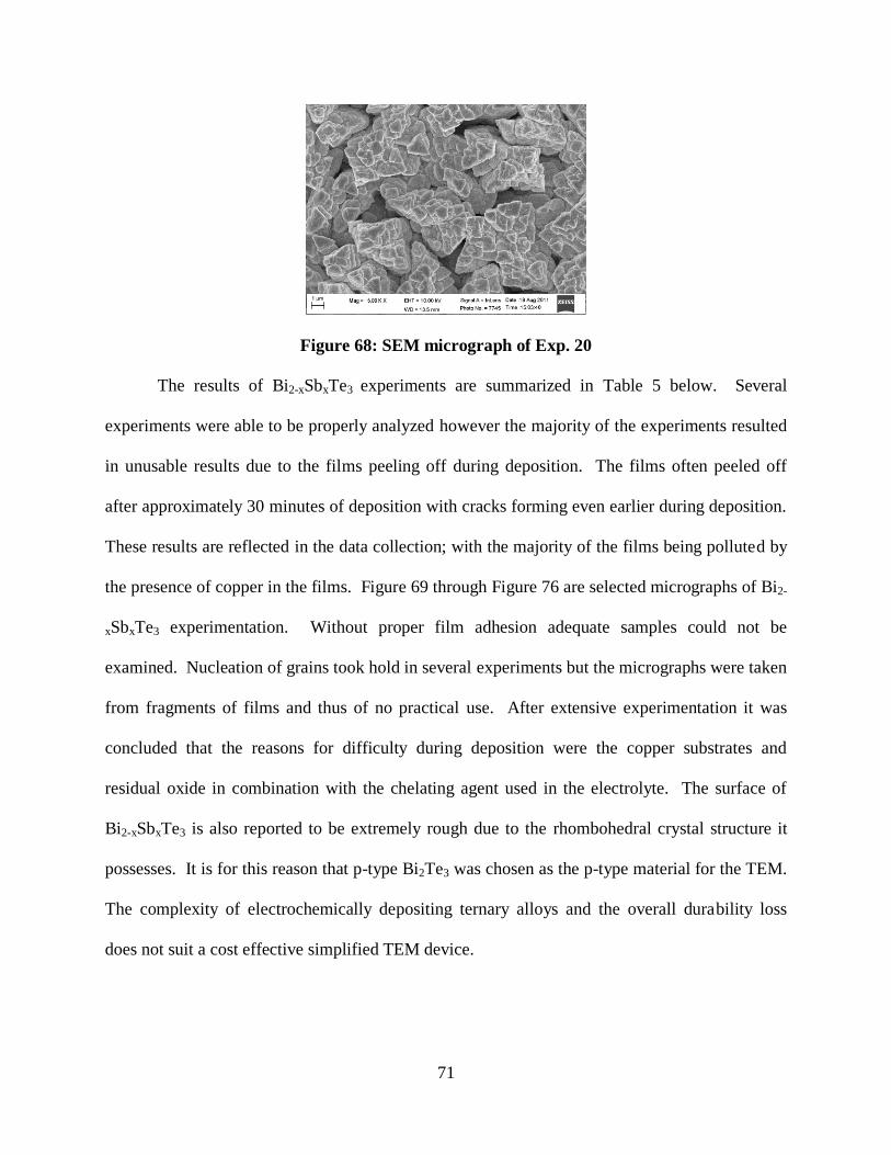
71
Figure 68: SEM micrograph of Exp. 20
The results of Bi2-xSbxTe3 experiments are summarized in Table 5 below. Several
experiments were able to be properly analyzed however the majority of the experiments resulted
in unusable results due to the films peeling off during deposition. The films often peeled off
after approximately 30 minutes of deposition with cracks forming even earlier during deposition.
These results are reflected in the data collection; with the majority of the films being polluted by
the presence of copper in the films. Figure 69 through Figure 76 are selected micrographs of Bi2-
xSbxTe3 experimentation. Without proper film adhesion adequate samples could not be
examined. Nucleation of grains took hold in several experiments but the micrographs were taken
from fragments of films and thus of no practical use. After extensive experimentation it was
concluded that the reasons for difficulty during deposition were the copper substrates and
residual oxide in combination with the chelating agent used in the electrolyte. The surface of
Bi2-xSbxTe3 is also reported to be extremely rough due to the rhombohedral crystal structure it
possesses. It is for this reason that p-type Bi2Te3 was chosen as the p-type material for the TEM.
The complexity of electrochemically depositing ternary alloys and the overall durability loss
does not suit a cost effective simplified TEM device.

72
Table 5: SEM and EDS results for Bi2-xSbxTe3 Experiments
Experiment Te at% Te at%
error (+/-)
Bi at% Bi at %
error (+/-)
Sb at% Sb at%
error (+/-)
Avg. Current
Density (mA/cm2)
24A 9.91 0.63 0.01 0.16 0.86 0.65 4
25A 38.89 2.06 7.81 0.57 21.87 3.32 5
26A 33.85 3.84 9.85 0.44 52.7 2.92 2
28A 34.2 0.75 8.39 0.28 8.19 0.64 2
33B* 66.45 -- 33.55 -- -- -- 2.7
34B* 78.09 -- 21.91 -- -- -- 2.8
37B* 15.1 -- 84.9 -- -- -- 2.7
39B* 73.13 -- 26.87 -- -- -- 3
40B* 70.64 -- 29.36 -- -- -- 2.7
41B* 97.37 -- 2.63 -- -- -- 2.7
Figure 69: SEM Micrographs for Exp. 24A
Figure 70: SEM Micrograph for Exp. 25A

73
Figure 71: SEM Micrograph for Exp. 33B
Figure 72: SEM micrograph for Exp. 34B
Figure 73: SEM micrograph for Exp. 37B
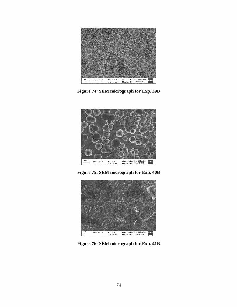
74
Figure 74: SEM micrograph for Exp. 39B
Figure 75: SEM micrograph for Exp. 40B
Figure 76: SEM micrograph for Exp. 41B

75
Modeling Results
The FEA results provide an important practical visualization that analytical models
simply cannot provide. Visual confirmation of theories provides foresight to potential problems
during production and operation. Using the analytical results as a guide to verify the results of
the FEA model proper vetting of a module design can be sought. In addition film properties
from established studies which were compared to the results from this study were used. For
processing of the model a mesh first needs to be selected. For the purposes of this model a mesh
of “normal” size was chosen for its combination of acceptable processing time and accuracy
definition in results. Even with coarsest mesh COMSOL offers only a 3% error would be
expected [28]. Figure 77 below shows the mesh on the TEM in COMSOL. Processing the
model provides steady state results that that largely agree with expected results for temperature
models shown in Figure 78 and Figure 79 below.
Figure 77: Mesh of thermoelectric module for COMSOL simulation

76
Figure 78: Surface temperature of TEM simulation
Figure 79: Volumetric temperature of TEM simulation
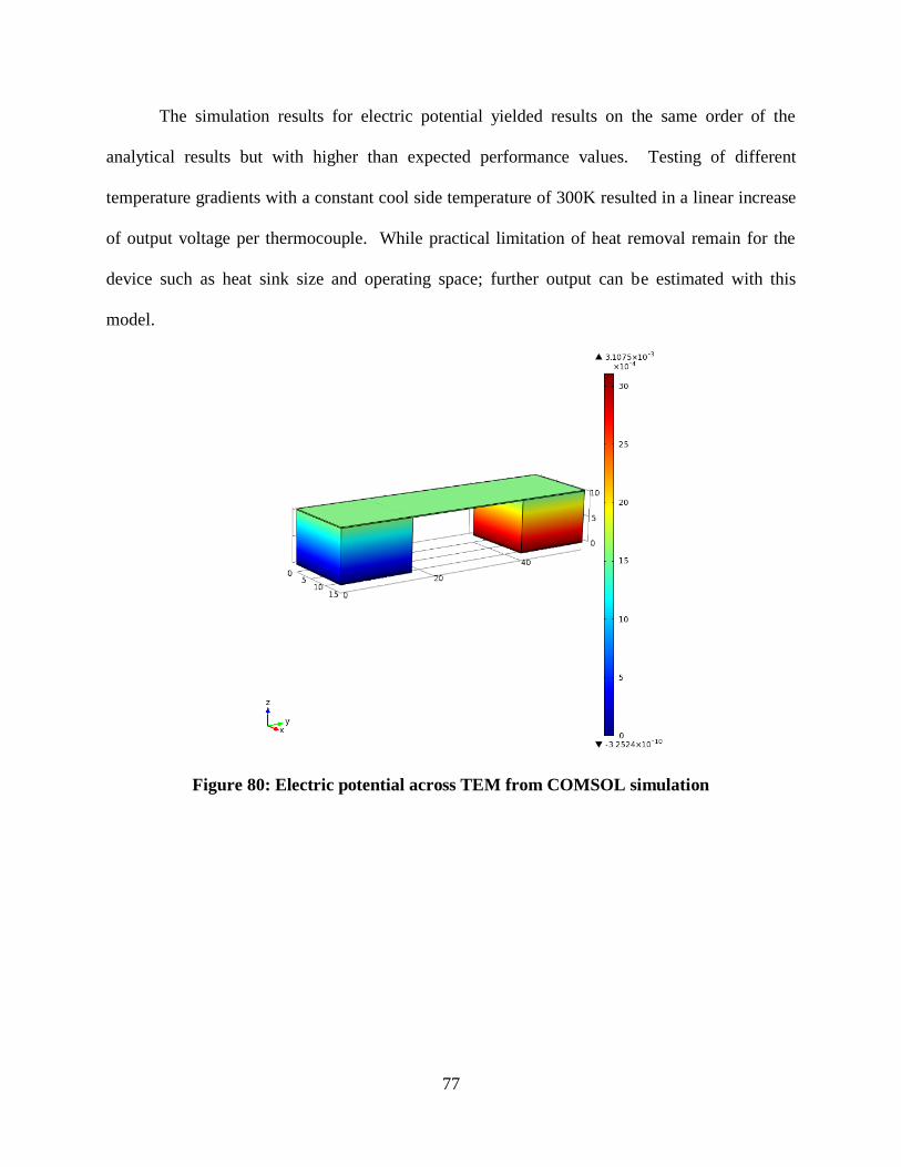
77
The simulation results for electric potential yielded results on the same order of the
analytical results but with higher than expected performance values. Testing of different
temperature gradients with a constant cool side temperature of 300K resulted in a linear increase
of output voltage per thermocouple. While practical limitation of heat removal remain for the
device such as heat sink size and operating space; further output can be estimated with this
model.
Figure 80: Electric potential across TEM from COMSOL simulation

78
Figure 81: FEA results for single couple with Tc=300 and variable Th
0
2
4
6
8
10
12
14
16
18
0 10 20 30 40 50 60 70
Voltage (mV)
Temperature Difference (K)
79
CHAPTER FIVE: CONCLUSIONS
This study investigated pertinent subjects concerning the optimization of micro
thermoelectric modules (TEMs) by examining thermoelectric thin film production, analytical
optimization results, finite element analysis, and processing optimizations. Fabrication of Bi2Te3
was done with an electrochemical deposition process which enabled control over a variety of
production variables. It was discovered that by controlling the average current density during
deposition, the Te at. % content can be controlled by a linear relationship, where an increase in
average current density corresponds with a lower Te content. Thermoelectric material was
deposited on to copper substrates under a variety of testing conditions; consequently, it was
found that Bi2Te3 was able to be deposited from a solution containing 8.2 mM Bi and 10.3 mM
Te in a 1M HNO3 solution with both AC and DC signals. In addition to investigating both n-
type and p-type Bi2Te3; p-type Bi2-xSbxTe3 was also investigated. After experimenting with a
variety of conditions and two electrolyte solutions, a usable film was unable to be produced
using copper substrates. This film type did not suit the device due to the complexity of
production and the low quality of the films produced. It is suspected that the amount of
impurities present from the chelating agent (tartaric acid), and residual oxide on the copper
surface contributed to the poor film quality.
Research of optimization equations yielded analytical and finite element equations that
were used to design both a testing device and a production device. The testing device created
would serve as a testing bed for optimization studies and material testing. The testing device
also utilized a conventional fabrication approach based on electrochemical deposition and a
monolithic topography. The optimized device had a unique topography that allowed for multiple
output voltages to be generated by an array of 0.5V unit cells at a temperature difference of 10K.

80
The fabrication process for the optimized TEM is drastically simplified and less expensive than
the process used for the testing device. The updated fabrication process uses a single electrolyte
bath, which can produce both n-type and p-type Bi2Te3, a thermoelectric material which operates
optimally near room temperatures. The conclusion that both n-type and p-type Bi2Te3 was
created is based on the Te content of the films, as well as previous studies linking Te content to
major carrier type. This processing procedure saves time and fabrication costs by reducing the
number of photoresist applications needed in order to produce a TEM; additionally, the need for
precious metals is eliminated by this fabrication procedure. FEA analysis of the device yielded
higher performance benchmarks than analytical analysis of the device. The increase in
performance was attributed to differences in load resistances and 3D effects.
Further improvement for TEMs lies in design improvements and advanced materials with
higher performance values. Segmented TEMs allow devices to operate over a larger temperature
range increasing their effective power output under large temperature gradients. Thermoelectric
devices benefit greatly from scaling and would see improvements in power density with scaling
devices to nano scale levels.

81
APPENDIX A: ORIGINAL DEVICE FABRICATION PROFILE

82
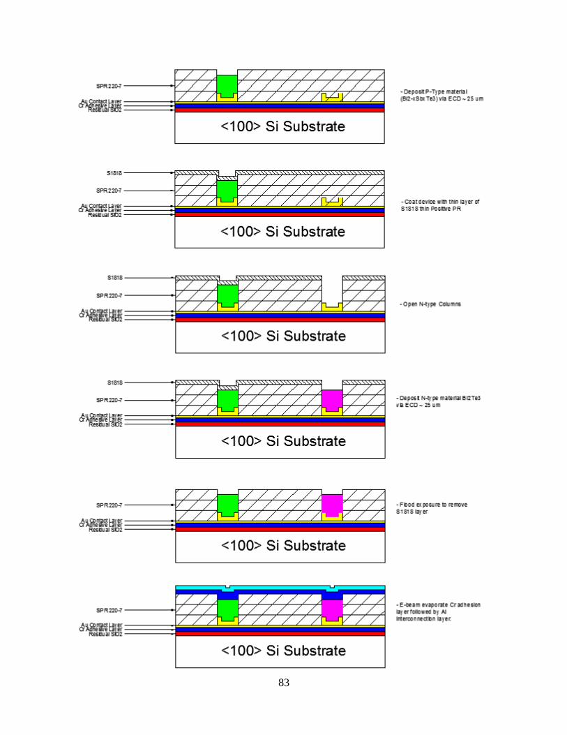
83

84

85
APPENDIX B: 10K DEVICE ANALYTICAL CALCULATIONS
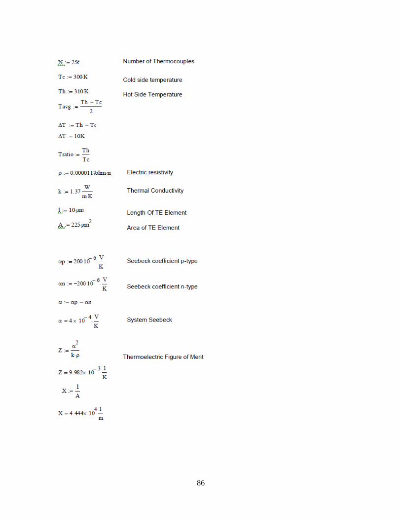
86

87

88
REFRENCES
[1] W. Fahrner, Semiconductor Thermoelectric Generators. Switzerland: Trans Tech
Publications Ltd., 2009.
[2] G. Min, "Thermoelectric Energy Harvesting," pp. 135-157, 2010 2010.
[3] J. P. Fleurial, et al., "Thick-film thermoelectric microdevices," in Thermoelectrics, 1999.
Eighteenth International Conference on, 1999, pp. 294-300.
[4] G. Savelli, "Energy Conversion Using New Thermoelectric Generator," DTIP of MEMS
& MOEMS, 2006.
[5] G. J. Snyder, et al., "Thermoelectric microdevice fabricated by a MEMS-like
electrochemical process," Nat Mater, vol. 2, pp. 528-531, 2003.
[6] M. Chen, et al., "On the Figure of Merit of Thermoelectric Generators," Journal of
Energy Resources Technology, vol. 127, pp. 37-41, 2005.
[7] S.-S. Lu and et al., "On the Figure of Merit of Thermoelectric Generators," Journal of
Energy Resources Technology, vol. 127, p. 37, 2005.
[8] R. A. Taylor and G. L. Solbrekken, "Comprehensive System-Level Optimization of
Thermoelectric Devices for Electronic Cooling Applications," Components and
Packaging Technologies, IEEE Transactions on, vol. 31, pp. 23-31, 2008.
[9] D. M. Rowe, Thermoelectrics handbook: macro to nano: CRC/Taylor & Francis, 2006.
[10] X. C. Xuan, "On the optimal design of multistage thermoelectric coolers," Semiconductor
Science and Technology, vol. 17, p. 625, 2002.
[11] T. Wartanowicz and A. Czarnecki, "Optimization of a multistage thermoelectric cooling
system concerning maximum COP," in Thermoelectrics, 1996., Fifteenth International
Conference on, 1996, pp. 307-310.
[12] J. R. Lin, et al., "Thermoelectric microdevice fabrication process and evaluation at the Jet
Propulsion Laboratory (JPL)," in Thermoelectrics, 2002. Proceedings ICT '02. Twenty-
First International Conference on, 2002, pp. 535-539.
[13] R. C. Jaeger, Introduction to microelectronic fabrication: Prentice Hall, 2002.
[14] J. Snyder. (07-1-2011). The Science of Thermoelectric Materials. Available:
http://www.thermoelectrics.caltech.edu/thermoelectrics/index.html
[15] D. M. Rowe, CRC handbook of thermoelectrics: CRC Press, 1995.
[16] M. J. Madou, Fundamentals of microfabrication: CRC Press, 1997.
[17] K. Tittes, et al., "Electrochemical deposition of Bi2Te3 for thermoelectric microdevices,"
Journal of Solid State Electrochemistry, vol. 7, pp. 714-723, 2003.
[18] Y. Miyazaki and T. Kajitani, "Preparation of Bi2Te3 films by electrodeposition," Journal
of Crystal Growth, vol. 229, pp. 542-546, 2001.
[19] C.-k. H. B.Y. Yoo, J.R. Lim et. al, "Electrochemically deposited thermoelectric n-type
Bi2Te3 thin films," Electrochimica Acta, vol. 50, pp. 4371-4377, 2005.
[20] C. B. P. Magri, J.M. Lecurie, J. Mater. Chem., p. 773, 1996.
[21] W.-j. Qiu, et al., "Additive-aided electrochemical deposition of bismuth telluride in a
basic electrolyte," International Journal of Minerals, Metallurgy, and Materials, vol. 17,
pp. 489-493, 2010.
[22] A.-H. B. K. Hesham M. A. Soliman, "Electrochemical Deposition and Optimization of
Thermoelectric Nanostructured Bismuth Telluride Thick Films," Engineering, vol. 3, pp.
659-667, May 28 2011.

89
[23] S.-K. Lim, et al., "Thermoelectric properties of the bismuth-antimony-telluride and the
antimony-telluride films processed by electrodeposition for micro-device applications,"
Thin Solid Films, vol. 517, pp. 4199-4203, 2009.
[24] F.-H. Li, et al., "Investigations on the electrodeposition behaviors of Bi0.5Sb1.5Te3 thin
film from nitric acid baths," Electrochimica Acta, vol. 54, pp. 3745-3752, 2009.
[25] M. S. Martin-Gonzalez, et al., "Insights into the Electrodeposition of Bi[sub 2]Te[sub
3]," Journal of The Electrochemical Society, vol. 149, pp. C546-C554, 2002.
[26] V. Richoux, et al., "Pulsed Electroplating: a Derivate Form of Electrodeposition for
Improvement of (Bi1-xSbx)2Te3 Thin Films," Journal of Electronic Materials, vol. 39,
pp. 1914-1919, 2010.
[27] W. D. Wijesooriyage, "Electrochemical Deposition and Characterization of
Thermoelectric Thin Films
of (BixSb1-x)2Te3," Master of Science, Department of Chemical and Biological Engineering,
CHALMERS UNIVERSITY OF TECHNOLOGY, Göteborg, 2011.
[28] E. J. Sandoz-Rosado, "Investigation and Development of Advanced Models of
Thermoelectric Generators for Power Generation
Applications," Master of Science, Department of Mechanical Engineering, Rochester Institute of
Technology, Rochester, 2009.
[29] D. Ebling, et al., "Multiphysics Simulation of Thermoelectric Systems for Comparison
with Experimental Device Performance," Journal of Electronic Materials, vol. 38, pp.
1456-1461, 2009.
[30] E. Sandoz-Rosado and R. Stevens, "Robust Finite Element Model for the Design of
Thermoelectric Modules," Journal of Electronic Materials, vol. 39, pp. 1848-1855, 2010.
![In‐situ TEM studies of nanostructured thermoelectric materials: … · cost and high conversion efficiency thermoelectric power generator (TEG).[22–28] Despite those advantages,](https://img.pdfslide.us/doc/110x75/5e37b76cded5da649801e808/inasitu-tem-studies-of-nanostructured-thermoelectric-materials-cost-and-high.jpg)