Embed Size (px)
Citation preview
PRESCRIPTION TO IMPROVE THERMOELECTRIC EFFICIENCY
A Thesis
by
SHIV AKARSH MEKA
Submitted to the Office of Graduate Studies of Texas A&M University
in partial fulfillment of the requirements for the degree of
MASTER OF SCIENCE
May 2010
Major Subject: Materials Science and Engineering
PRESCRIPTION TO IMPROVE THERMOELECTRIC EFFICIENCY
A Thesis
by
SHIV AKARSH MEKA
Submitted to the Office of Graduate Studies of Texas A&M University
in partial fulfillment of the requirements for the degree of
MASTER OF SCIENCE
Approved by:
Chair of Committee, Tahir Cagin
Committee Members, Donald Naugle Jun Kameoka
Chair of Materials Science and Engineering Faculty, Tahir Cagin
May 2010
Major Subject: Materials Science and Engineering
iii
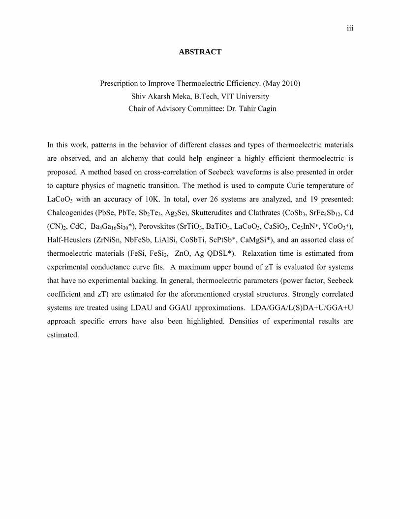
ABSTRACT
Prescription to Improve Thermoelectric Efficiency. (May 2010)
Shiv Akarsh Meka, B.Tech, VIT University Chair of Advisory Committee: Dr. Tahir Cagin
In this work, patterns in the behavior of different classes and types of thermoelectric materials
are observed, and an alchemy that could help engineer a highly efficient thermoelectric is
proposed. A method based on cross-correlation of Seebeck waveforms is also presented in order
to capture physics of magnetic transition. The method is used to compute Curie temperature of
LaCoO3 with an accuracy of 10K. In total, over 26 systems are analyzed, and 19 presented:
Chalcogenides (PbSe, PbTe, Sb2Te3, Ag2Se), Skutterudites and Clathrates (CoSb3, SrFe4Sb12, Cd
(CN)2, CdC, Ba8Ga16Si30*), Perovskites (SrTiO3, BaTiO3, LaCoO3, CaSiO3, Ce3InN*, YCoO3*),
Half-Heuslers (ZrNiSn, NbFeSb, LiAlSi, CoSbTi, ScPtSb*, CaMgSi*), and an assorted class of
thermoelectric materials (FeSi, FeSi2, ZnO, Ag QDSL*). Relaxation time is estimated from
experimental conductance curve fits. A maximum upper bound of zT is evaluated for systems
that have no experimental backing. In general, thermoelectric parameters (power factor, Seebeck
coefficient and zT) are estimated for the aforementioned crystal structures. Strongly correlated
systems are treated using LDAU and GGAU approximations. LDA/GGA/L(S)DA+U/GGA+U
approach specific errors have also been highlighted. Densities of experimental results are
estimated.

iv
To my parents Dr.Shankar & Dr.Padma
and to my foster parents at A&M: Dr. Tahir and Jan
v
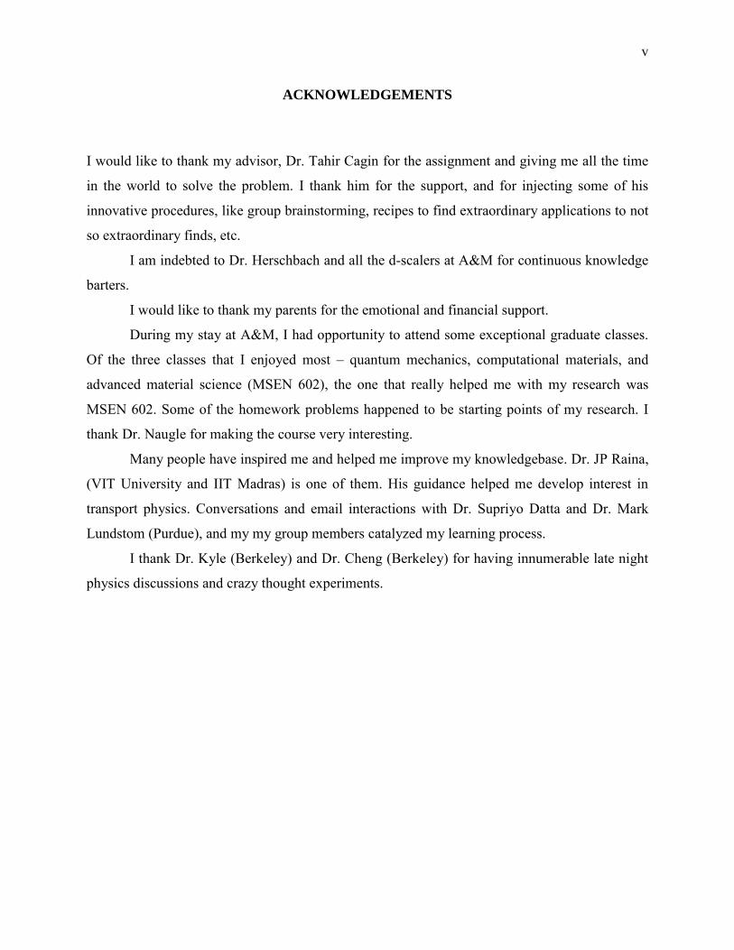
ACKNOWLEDGEMENTS
I would like to thank my advisor, Dr. Tahir Cagin for the assignment and giving me all the time
in the world to solve the problem. I thank him for the support, and for injecting some of his
innovative procedures, like group brainstorming, recipes to find extraordinary applications to not
so extraordinary finds, etc.
I am indebted to Dr. Herschbach and all the d-scalers at A&M for continuous knowledge
barters.
I would like to thank my parents for the emotional and financial support.
During my stay at A&M, I had opportunity to attend some exceptional graduate classes.
Of the three classes that I enjoyed most – quantum mechanics, computational materials, and
advanced material science (MSEN 602), the one that really helped me with my research was
MSEN 602. Some of the homework problems happened to be starting points of my research. I
thank Dr. Naugle for making the course very interesting.
Many people have inspired me and helped me improve my knowledgebase. Dr. JP Raina,
(VIT University and IIT Madras) is one of them. His guidance helped me develop interest in
transport physics. Conversations and email interactions with Dr. Supriyo Datta and Dr. Mark
Lundstom (Purdue), and my my group members catalyzed my learning process.
I thank Dr. Kyle (Berkeley) and Dr. Cheng (Berkeley) for having innumerable late night
physics discussions and crazy thought experiments.

vi
NOMENCLATURE
Symbols
e Electron charge
E Energy eigenvalue
Eg Bandgap (eV)
f0 Equilibrium Fermi function
fμ Fermi-function at μ
Ĥ Hamiltonian operator
ħ Planck's constant
k Thermal conductivity (W/m•K)
ke Electrical contribution to the thermal conductivity (W/m•K)
kl Lattice thermal conductivity (W/m•K)
m mass of an electron
m* effective mass
n Carrier concentration
pf Power factor
S Seebeck coefficient
T Temperature (K)
U Nuclear-electron interaction operator
V External interaction potential operator
zT Thermoelectric figure of merit
μm Carrier mobility
∆ Laplacian operator
ρ Resistivity (Ω/cm)
σ Electrical conductivity (S/cm)
υ Kohn-Sham one-particle wavefunction
Ψ Electron wavefunction
vii
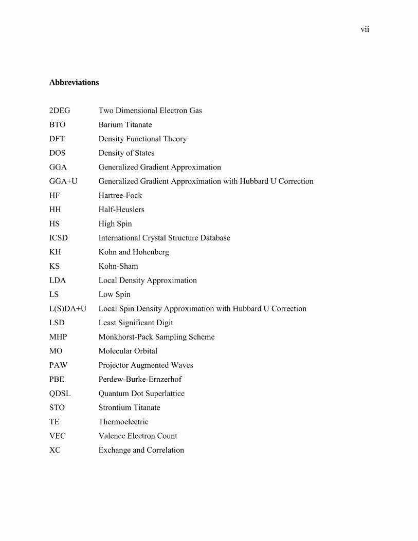
Abbreviations
2DEG Two Dimensional Electron Gas
BTO Barium Titanate
DFT Density Functional Theory
DOS Density of States
GGA Generalized Gradient Approximation
GGA+U Generalized Gradient Approximation with Hubbard U Correction
HF Hartree-Fock
HH Half-Heuslers
HS High Spin
ICSD International Crystal Structure Database
KH Kohn and Hohenberg
KS Kohn-Sham
LDA Local Density Approximation
LS Low Spin
L(S)DA+U Local Spin Density Approximation with Hubbard U Correction
LSD Least Significant Digit
MHP Monkhorst-Pack Sampling Scheme
MO Molecular Orbital
PAW Projector Augmented Waves
PBE Perdew-Burke-Ernzerhof
QDSL Quantum Dot Superlattice
STO Strontium Titanate
TE Thermoelectric
VEC Valence Electron Count
XC Exchange and Correlation
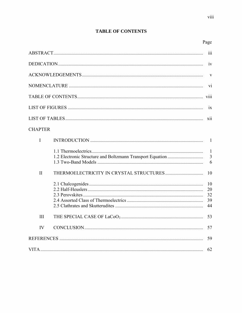
viii
TABLE OF CONTENTS
Page
ABSTRACT .............................................................................................................................. iii
DEDICATION .......................................................................................................................... iv
ACKNOWLEDGEMENTS ...................................................................................................... v
NOMENCLATURE ................................................................................................................. vi
TABLE OF CONTENTS .......................................................................................................... viii
LIST OF FIGURES .................................................................................................................. ix
LIST OF TABLES .................................................................................................................... xii
CHAPTER
I INTRODUCTION ............................................................................................... 1 1.1 Thermoelectrics.............................................................................................. 1 1.2 Electronic Structure and Boltzmann Transport Equation .............................. 3 1.3 Two-Band Models ......................................................................................... 6 II THERMOELECTRICITY IN CRYSTAL STRUCTURES ................................ 10
2.1 Chalcogenides ................................................................................................ 10 2.2 Half-Heuslers ................................................................................................. 20 2.3 Perovskites ..................................................................................................... 32 2.4 Assorted Class of Thermoelectrics ................................................................ 39 2.5 Clathrates and Skutterudites .......................................................................... 44
III THE SPECIAL CASE OF LaCoO3 ..................................................................... 53
IV CONCLUSION .................................................................................................... 57
REFERENCES ......................................................................................................................... 59
VITA ......................................................................................................................................... 62
ix
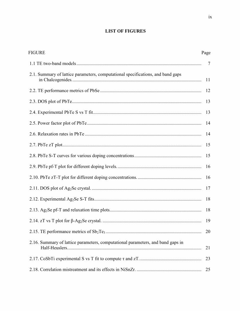
LIST OF FIGURES
FIGURE Page
1.1 TE two-band models .......................................................................................................... 7
2.1. Summary of lattice parameters, computational specifications, and band gaps in Chalcogenides. ............................................................................................................. 11
2.2. TE performance metrics of PbSe ...................................................................................... 12
2.3. DOS plot of PbTe.............................................................................................................. 13
2.4. Experimental PbTe S vs T fit ............................................................................................ 13
2.5. Power factor plot of PbTe ................................................................................................. 14
2.6. Relaxation rates in PbTe ................................................................................................... 14
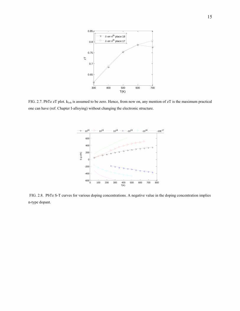
2.7. PbTe zT plot ...................................................................................................................... 15
2.8. PbTe S-T curves for various doping concentrations ......................................................... 15
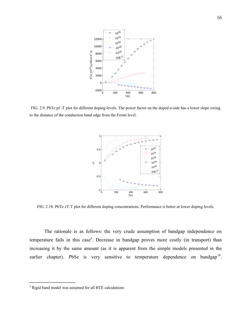
2.9. PbTe pf-T plot for different doping levels. ....................................................................... 16
2.10. PbTe zT-T plot for different doping concentrations. ...................................................... 16
2.11. DOS plot of Ag2Se crystal. ............................................................................................. 17
2.12. Experimental Ag2Se S-T fits ........................................................................................... 18
2.13. Ag2Se pf-T and relaxation time plots.............................................................................. 18
2.14. zT vs T plot for β-Ag2Se crystal. .................................................................................... 19
2.15. TE performance metrics of Sb2Te3 ................................................................................. 20
2.16. Summary of lattice parameters, computational parameters, and band gaps in Half-Heuslers. ................................................................................................................. 21
2.17. CoSbTi experimental S vs T fit to compute τ and zT. .................................................... 23
2.18. Correlation mistreatment and its effects in NiSnZr. ....................................................... 25
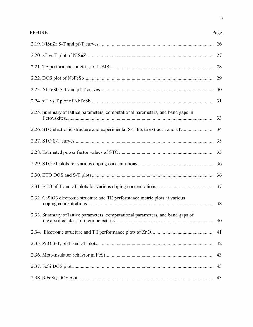
x
FIGURE Page
2.19. NiSnZr S-T and pf-T curves. .......................................................................................... 26
2.20. zT vs T plot of NiSnZr .................................................................................................... 27
2.21. TE performance metrics of LiAlSi. ................................................................................ 28
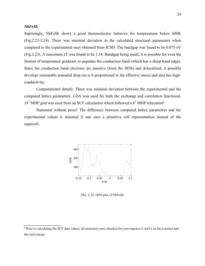
2.22. DOS plot of NbFeSb ....................................................................................................... 29
2.23. NbFeSb S-T and pf-T curves .......................................................................................... 30
2.24. zT vs T plot of NbFeSb .................................................................................................. 31
2.25. Summary of lattice parameters, computational parameters, and band gaps in Perovskites ...................................................................................................................... 33
2.26. STO electronic structure and experimental S-T fits to extract τ and zT. ........................ 34
2.27. STO S-T curves............................................................................................................... 35
2.28. Estimated power factor values of STO ........................................................................... 35
2.29. STO zT plots for various doping concentrations ............................................................ 36
2.30. BTO DOS and S-T plots ................................................................................................. 36
2.31. BTO pf-T and zT plots for various doping concentrations ............................................. 37
2.32. CaSiO3 electronic structure and TE performance metric plots at various doping concentrations ..................................................................................................... 38
2.33. Summary of lattice parameters, computational parameters, and band gaps of
the assorted class of thermoelectrics .............................................................................. 40 2.34. Electronic structure and TE performance plots of ZnO. ................................................ 41
2.35. ZnO S-T, pf-T and zT plots. ........................................................................................... 42
2.36. Mott-insulator behavior in FeSi ...................................................................................... 43
2.37. FeSi DOS plot ................................................................................................................. 43
2.38. β-FeSi2 DOS plot. ........................................................................................................... 43
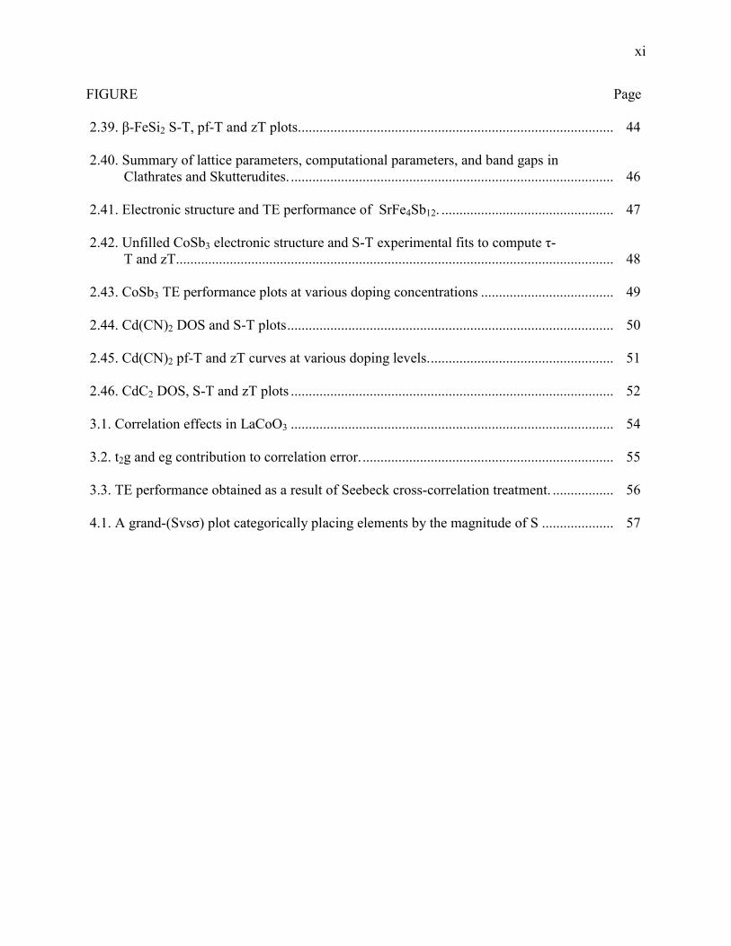
xi
FIGURE Page
2.39. β-FeSi2 S-T, pf-T and zT plots. ....................................................................................... 44
2.40. Summary of lattice parameters, computational parameters, and band gaps in Clathrates and Skutterudites. .......................................................................................... 46
2.41. Electronic structure and TE performance of SrFe4Sb12. ................................................ 47
2.42. Unfilled CoSb3 electronic structure and S-T experimental fits to compute τ-T and zT .......................................................................................................................... 48
2.43. CoSb3 TE performance plots at various doping concentrations ..................................... 49
2.44. Cd(CN)2 DOS and S-T plots ........................................................................................... 50
2.45. Cd(CN)2 pf-T and zT curves at various doping levels. ................................................... 51
2.46. CdC2 DOS, S-T and zT plots .......................................................................................... 52
3.1. Correlation effects in LaCoO3 .......................................................................................... 54
3.2. t2g and eg contribution to correlation error. ...................................................................... 55
3.3. TE performance obtained as a result of Seebeck cross-correlation treatment. ................. 56
4.1. A grand-(Svsσ) plot categorically placing elements by the magnitude of S .................... 57

xii
LIST OF TABLES
TABLE Page
1.1 Possible permutations of varying magnitudes of mcb and mvb ................................... 6
2.1 Comparison of wall times between Clathrates and highly-symmetric Chalcogenides ............................................................................................................ 50 3.1 LaCoO3 d-electron occupancies in LS, and spin polarized HS states ........................ 54

1
CHAPTER I
INTRODUCTION
1.1 Thermoelectrics
The current demand for energy is creating social and political unrest. One way to go about the
problem is to squeeze the fruit till the last drop. Thermoelectrics do just this! They perform the
last rites by scavenging waste heat. Car exhausts, geothermal energy, home heating, industries
and microchips are sources where the systems get thermally equilibrated before being put to
good use. Scavenger engineering has been one of the challenges of the recent past. A plethora of
materials and alloys leads to confusion on choosing an ideal material to be used as a
thermoelectric. A rational approach would be to observe patterns of behavior of different classes
of heat-scavengers and capture the physics to understand the rationale behind the working of
these devices. Also, the quality of thermoelectric conversion has to be expressed in numbers so
that one would be able to compare between two given samples and observe empirical patterns
that could even help on improving the efficiency. Mathematically, the figure of merit (zT) sums
it all: zT=S2σT/k where S is the Seebeck coefficient which quantifies the potential change due to
a temperature gradient, σ is the conductivity , T, the temperature, and k , the thermal
conductivity. While S is directly proportional to the open circuit voltage ΔV developed across
the structure that has just a temperature gradient ΔT (S= ΔV/ ΔT), the power factor (pf= 𝑆2𝜍
𝜏) is
the closed circuit current and depends on the conductivity, 𝜍. In order to maximize the function
zT, one needs to have both Seebeck coefficient and the electrical conductivity high, and k low.
But this is contradicting. How can something develop a high emf and even pump current? The
subtlety is: the overall product is what matters. But, it is a reasonable assumption since one needs
not just a voltage difference developed, but the circuit ought to be closed or there could be
charge buildup finally breaking the dielectric (for very low values of 𝜍 ). Beginning with
This thesis follows the style and format of Physical Review B.

2
thermocouples, thermoelectrics have a very long history. Recent trends in nanostructured
materials improved efficiency 4 folds.
Doping
Type of carriers involved in the transport plays a crucial role in determining the efficiency of a
thermoelectric. In general, it is advised to have higher concentration of carriers of one type.
Bipolar carrier recombination adds to k which degrades the performance of the thermoelectric.
One carrier type must dominate in order to have maximum S. Mixed conduction cancels out the
net effect of charge flow as one carrier moves to the hot end and the other to the cold. Low
concentration means low conductivity. Conductivity and Seebeck coefficients could be deduced
from two-band models as briefed in the forthcoming section. In general, Seebeck coefficient and
conductivity are given by:
𝑆 =8𝜋2𝑘𝐵
2
3𝑒2𝑚∗𝑇
𝜋
3𝑛
23
;
1
𝜌= 𝜍 = 𝑛𝑒𝜇𝑚
where m* is the effective mass, and n, the carrier concentration.
Conductivity
According to Wiedemann-Franz law: (𝜅𝑒 = 𝐿𝜍𝑇 = 𝑛𝑒𝜇𝑚𝐿𝑇, Lorentz factor L=2.4 10-8 J2 K-2
C-2), ke is the electronic contribution to the total thermal conductivity k=ke+kl with the lattice
thermal conductivity kl. Charge carriers transport heat as do phonons. In Chapter II, zT is
computed under the assumption that the scattering time due to electrons and phonons are equal.
This crude assumption enables to find an upper bound for maximum value of zT at zero kl. For
most systems, kl is above 75% contribution of the total k, and is generally unaffected by carrier
concentration. Glasses are known for low kla. But, electrons in glasses are scattered very strongly
making them poor thermoelectrics.
Low or high m*?
From the simple Drude model, large m* means good S but a bad σ. So, mobility is an important
a In glasses, the mean free path of phonons equals the inter-atomic distance, which of course, is not constant. Phonon
description does no good in describing kl. A random walk description guarantees minimal kl. The reader is advised
to read Kittel’s1 perspective on thermal conductivity in glasses.
3
factor in thermoelectric design. m* is directly proportional to the density of states. Flat bands
(large m*) mean confined electrons with a high S. Dephasing issues and lattice thermal
conductivity, scattering, and anisotropy are a summed up contribution in the overall
performance. Large m* with low conductivity (for eg.:Chalcogenides) are a result of small
electronegativity differences while small m* and large conductivity are a result of large
electronegativity differences, but both can have a good zT.
Bottom line
One needs a “phonon-glass and an electron crystal”2 to realize a close to ideal thermoelectric.
Glass like properties are achieved by scattering phonons, engineering scattering centers and
making solid-solutions. Clathrates, filled skutterudites, Quantum dot super-lattices (QDSLs),
Zintl phases have so far been identified as potential candidates in the high-zT region of
thermoelectric operation.
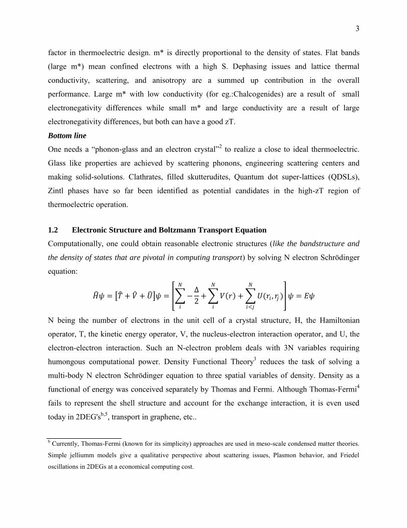
1.2 Electronic Structure and Boltzmann Transport Equation
Computationally, one could obtain reasonable electronic structures (like the bandstructure and
the density of states that are pivotal in computing transport) by solving N electron Schrödinger
equation:
𝐻 𝜓 = 𝑇 + 𝑉 + 𝑈 𝜓 = −Δ
2+
𝑁
𝑖
𝑉 𝑟
𝑁
𝑖
+ 𝑈(𝑟𝑖 , 𝑟𝑗 )
𝑁
𝑖<𝑗
𝜓 = 𝐸𝜓
N being the number of electrons in the unit cell of a crystal structure, H, the Hamiltonian
operator, T, the kinetic energy operator, V, the nucleus-electron interaction operator, and U, the
electron-electron interaction. Such an N-electron problem deals with 3N variables requiring
humongous computational power. Density Functional Theory3 reduces the task of solving a
multi-body N electron Schrödinger equation to three spatial variables of density. Density as a
functional of energy was conceived separately by Thomas and Fermi. Although Thomas-Fermi4
fails to represent the shell structure and account for the exchange interaction, it is even used
today in 2DEG'sb,5, transport in graphene, etc..
b Currently, Thomas-Fermi (known for its simplicity) approaches are used in meso-scale condensed matter theories.
Simple jelliumm models give a qualitative perspective about scattering issues, Plasmon behavior, and Friedel
oscillations in 2DEGs at a economical computing cost.

4
DFT was put forward by two simple yet far-reaching theorems by Kohn and Hohenberg.
Field perturbations and degeneracy were not taken into account in the original theorem they
proposed, but eventually showed up in a refined model later on. Excited state approaches and
external perturbation became add-ons in the form of time-dependent DFT.
The second KH theorem3 states that the exact density minimizes the energy functional
which is sum of the kinetic, Coulomb, Fock and Correlation functionals6, while the first theorem
maps the N variable problem into N “independent” equations, each of which results in a three
variable density function. Density functional theory simplifies the N-particle interacting problem
into non-interacting particles moving in an effective potential that includes the contribution due
to Coulomb interaction. While the kinetic energy (which is a major portion of the total energy) is
calculated exactly using this formalism, exchange and correlation has been a problem for the past
3 decades of its inception. There are hundreds of papers dealing with the proper functional form
of the exchange and correlation. Hartree-Fock6 for example, naturally treats exchange and it is
for this reason that DFT uses a very similar Fock (Slater) like term. The initial functional
(LDA7 𝐸𝑥𝑐𝑎𝑛𝑔𝑒 − 𝐶𝑜𝑟𝑟𝑒𝑙𝑎𝑡𝑖𝑜𝑛 𝑓𝑢𝑛𝑐𝑡𝑖𝑜𝑛𝑎𝑙 𝐸𝑥𝑐 = 𝑑3𝑟 𝜖𝑥𝑐 𝑛↓, 𝑛↑ 𝑛(𝑟) assumed a uniform
electron gas (advanced Thomas-Fermi model). The correlation functional in the LDA regime
looks like: 휀𝑐 = 𝐴𝑙𝑛 𝑟𝑠 + 𝐵 + 𝑟𝑠(𝐶𝑙𝑛 𝑟𝑠 + 𝐷), A,B,C,D are parameterized constants, and rs is
the Wigner-Sietz7 radius. And even the advanced GGA7 approach employs a similar functional
term except that it has derivatives of the density (applicable where density changes abruptly like
in metals).
The DFT Procedure
Any observable (like energy, momentum, etc.) O could be written as:
𝑂 𝑛0 = 𝜓[𝑛0] 𝑂 𝜓[𝑛0]
and the ground state energy which is a functional of exact density n0 is given as :
𝐸0 = 𝐸 𝑛0 = 𝜓[𝑛0] 𝑇 + 𝑉 + 𝑈 𝜓[𝑛0]
The external potential 𝜓 𝑉 𝜓 is written as: (here is where one lumps the correlation into some
functional form)
𝑉 𝑛0 = 𝑉 𝑟 𝑛𝑜 (𝑟)𝑑3𝑟
T[n] and U[n] are independent of the type of nucleus (atomic number) and hence are called
universal functionals. And it is now enough to minimize the functional:
5
𝐸 𝑛 = 𝑇 𝑛 + 𝑈[𝑛] + 𝑉 𝑟 𝑛𝑜 (𝑟)𝑑3𝑟]
Initially, one solves the energy functional without an explicit e-e term for each shell s:
𝐸𝑠 𝑛0 = 𝜓𝑠[𝑛] 𝑇 𝑠 + 𝑉 𝑠 𝜓𝑠[𝑛]
where 𝑉 𝑠 = 𝑉 + 𝑈 + (𝑇 − 𝑇 𝑠) and Ts is the kinetic energy operator of the shell s, and the
optimization rules that include the xc effects, help minimize the kinetic energy. One then solves
s-shell single particle non-interacting system (Kohn-Sham Hamiltonian): (in atomic units)
−Δ + 𝑉𝑠 𝑟 𝜙𝑖 𝑟 = 휀𝑖𝜙𝑖 𝑟
where the density and Vs are given by:
𝑛 𝑟 = 𝑛𝑠 𝑟 = 𝜙𝑖 𝑟 2
𝑁
𝑖
𝑉𝑠 𝑟 = 𝑉 𝑟 + 𝑛𝑠(𝑟 ′ )
𝑟−𝑟′ 𝑑3𝑟′ + 𝑉𝑥𝑐 [𝑛𝑠 𝑟 ].
The trick used to compute guess density is to superpose the already parameterized atom-
dependent basis sets. A linear combination of these basis functions produce molecular orbitals
(MO coefficients) or energy bands. The optimization Hessian has values corresponding to the
mixing rules. Vs obtained, is supplied as input to the KS Hamiltonian. This process reiterates
until the convergence (difference of successive ε’s < tolerance) is reached.
Boltzmann Transport8
As with the continuity equation, the value [Av(x)g(x)dt-Av(x+dx)g(x+dx)dt]- represents the
number of particles between g(x+dx) and g(x) [with g being the density] flowing perpendicular
to the plane of area A with velocity v(x) at g(x) and v(x+dx) at g(x+dx). And hence, 𝑑𝑔
𝑑𝑡=
−𝑑
𝑑𝑥(𝑣 𝑥 𝑔 𝑥, 𝑡 ).
To the above equation, Boltzmann added a viscous term that includes the effect of
scattering and hence 𝑑𝑔𝑑𝑡
=−𝑑
𝑑𝑥 𝑣 𝑥 𝑔 𝑥, 𝑡 + 𝑑𝑔
𝑑𝑡 𝑐𝑜𝑙𝑙
In the Hamilton notationc , the group velocity of an electron is given as:
𝑣 𝑖, 𝑘 = ∇kεi,k .
c Dirac’s prelude
9 to quantum mechanics is an excellent description of the connection with Hamilton formulation.
6
The conductivity could be defined as: ∑(v2) DOS(E) or more precisely:
𝜍 𝛼𝛽 휀 =1
𝑁 𝜏 ∙ 𝜈𝛼 𝑖, 𝑘 ∙ 𝜈𝛽 𝑖, 𝑘 𝑖 ,𝑘 ∙
𝛿 휀−휀𝑖 ,𝑘
𝑑휀 (1)
and Seebeck coefficient is given by :
𝑆𝛼 ,𝛽 𝑇, 𝜇 =1
𝑇Ω𝜍 𝛼𝛽 𝑇,𝜇 𝜍 𝛼𝛽 휀 휀 − 𝜇 −
𝜕𝑓0(𝑇,휀 ,𝜇)
𝜕휀 𝑑휀 (2)
where μ is the electrochemical potential, fo is the Fermi function, εi,k, the energy of ith band and
kth k-space sample, Ω the volume of the unit-cell and 𝜕𝑓0
𝜕휀 is the thermal broadening function
which smears the discrete energy levels.
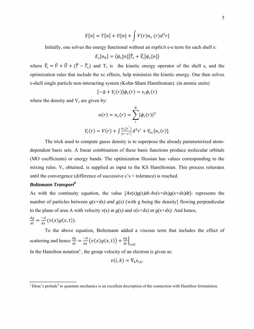
1.3 Two-Band Models
Equations (1) and (2) are used to compute S vs T curves (Fig.1.1) for different configurations
(Table.1.1).
TABLE 1.1. Possible permutations of varying magnitudes of mcb and mvb. Types of possible
configurations mcb and mvb are effective masses of conduction band and valence band. The figure
fig.1.1 summarizes the behavior of various combinations of effective masses, position of the
Fermi energy and bandgaps to determine the behavior of Seebeck coefficient. Most of the
systems in the forthcoming chapters could be explained by these simple two band models.
Type Description
A Small bandgap and Fermi positioned symmetrically, small m*
B Large bandgap and Fermi positioned symmetrically, large m*
C Large bandgap and Fermi positioned symmetrically, small m*
D Small bandgap and Fermi positioned symmetrically, mcb > mvb
E Large bandgap, and Fermi positioned symmetrically, mvb > mcb
F Small bandgap, and Fermi positioned symmetrically, mvb > mcb
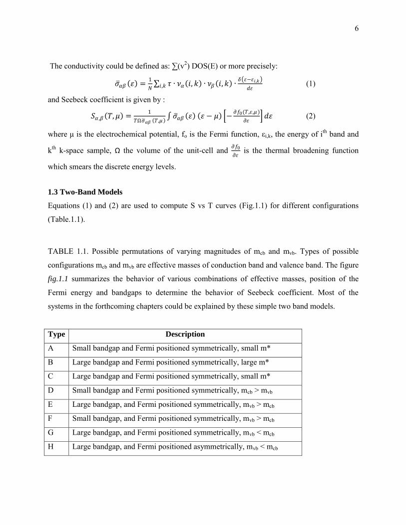
G Large bandgap, and Fermi positioned symmetrically, mvb < mcb
H Large bandgap, and Fermi positioned asymmetrically, mvb < mcb
7
TABLE 1.1 Continued.
Type Description
I High bandgap, and Fermi positioned symmetrically, mvb = mcb
J Small bandgap, and Fermi positioned asymmetrically, mvb = mcb
FIG. 1.1. TE Two-band models. Density of states (DOS (ε-μ)), band-structure and Seebeck coefficient S(ε-μ) plots
of crystal structures with a) narrow bandgap small m* b) narrow bandgap large m* c) large bandgap, small m* d)
narrow bandgap, small mvb large mcb .
-15 -10 -5 0 5 10 150
0.5
1
1.5
2
E(eV)
DO
S
-10 -5 0 5 10-15
-10
-5
0
5
10
15
k
E(e
V)
-4 -2 0 2 4 6-400
-200
0
200
400
E(eV)
S
-3 -2 -1 0 1 2 30
5
10
15
E(eV)
DO
S
-10 -5 0 5 10-3
-2
-1
0
1
2
3
k
E(e
V)
-4 -2 0 2 4 6-60
-40
-20
0
20
40
60
E(eV)
S
-20 -10 0 10 200
0.5
1
1.5
2
E(eV)
DO
S
-10 -5 0 5 10-20
-10
0
10
20
k
E(e
V)
-4 -2 0 2 4 6-500
0
500
E(eV)
S
-15 -10 -5 0 50
2
4
6
8
10
E(eV)
DO
S
-10 -5 0 5 10-15
-10
-5
0
5
k
E(e
V)
-4 -2 0 2 4 6-100
0
100
200
300
400
E(eV)
S
8
FIG. 1.1 Continued. e) large bandgap , small mvb, large mcb f) Fermi positioned at zero for narrow bandgap, large
mvb small mcb results in S(-) g) Fermi brought close to VB results in decrease of S(+) h) Fermi positioned at VB
results in large S(+) for large mcb and small mvb i) Fermi at zero in the wide bandgap crystal with both mvb and mcb
high..
-10 -5 0 5 10 15 200
2
4
6
8
E(eV)
DO
S
-10 -5 0 5 10-10
-5
0
5
10
15
20
k
E(e
V)
-4 -2 0 2 4 6-500
-400
-300
-200
-100
0
100
200
E(eV)
S
-5 0 5 10 150
2
4
6
8
10
E(eV)
DO
S
-10 -5 0 5 10-5
0
5
10
15
k
E(e
V)
-4 -2 0 2 4 6-400
-300
-200
-100
0
100
E(eV)
S
-20 -15 -10 -5 0 5 100
2
4
6
8
E(eV)
DO
S
-10 -5 0 5 10-20
-15
-10
-5
0
5
10
k
E(e
V)
-4 -2 0 2 4 6-200
-100
0
100
200
300
400
500
E(eV)
S
-15 -10 -5 0 5 100
2
4
6
8
E(eV)
DO
S
-10 -5 0 5 10-15
-10
-5
0
5
10
k
E(e
V)
-4 -2 0 2 4 6-200
-100
0
100
200
300
400
E(eV)
S
-3 -2 -1 0 1 2 30
10
20
30
40
50
E(eV)
DO
S
-10 -5 0 5 10-3
-2
-1
0
1
2
3
k
E(e
V)
-4 -2 0 2 4 6-100
-50
0
50
100
E(eV)
S
9
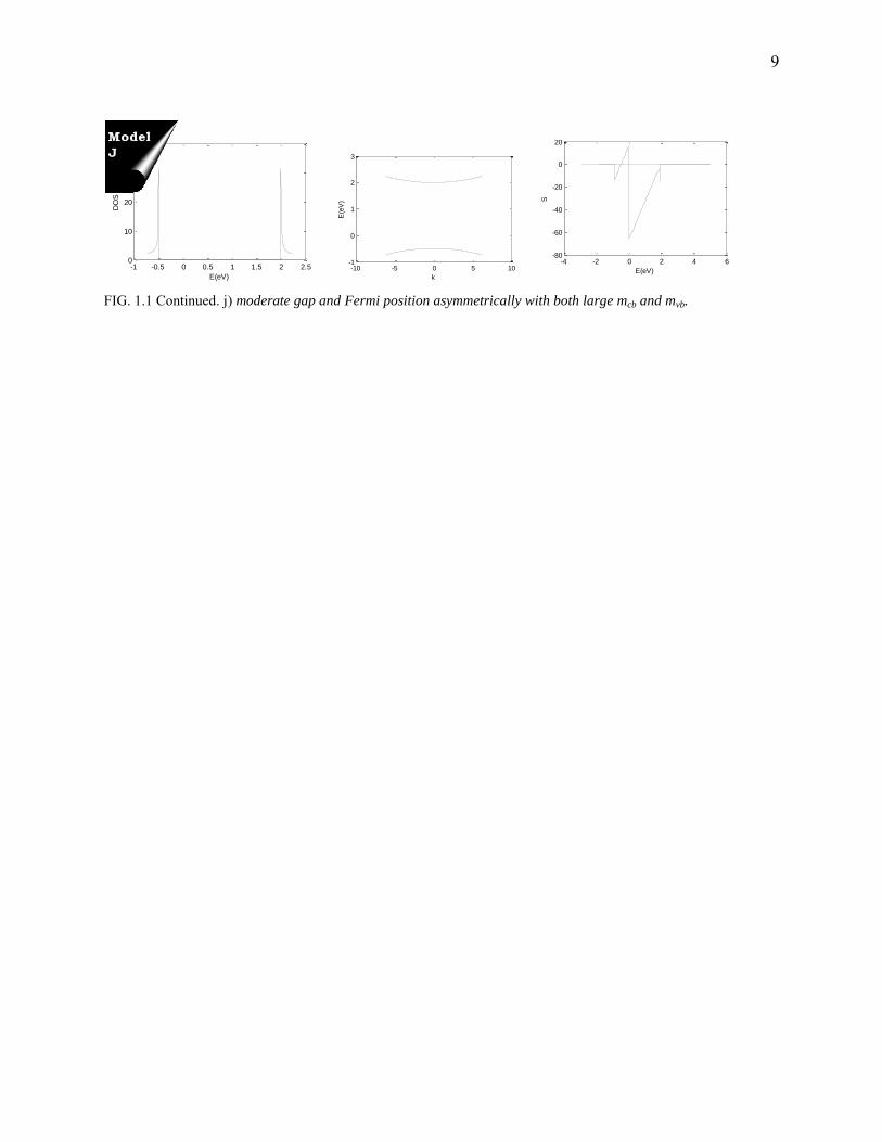
FIG. 1.1 Continued. j) moderate gap and Fermi position asymmetrically with both large mcb and mvb.
-1 -0.5 0 0.5 1 1.5 2 2.50
10
20
30
40
E(eV)
DO
S
-10 -5 0 5 10-1
0
1
2
3
k
E(e
V)
-4 -2 0 2 4 6-80
-60
-40
-20
0
20
E(eV)
S

10
CHAPTER II
THERMOELECTRICITY IN CRYSTAL STRUCTURES
2.1 Chalcogenides
A binary compound with one element derived from the group XVI is classified as a
Chalcogenide. There are exceptions, however, for example, oxides. But, in general, Selenides
and Tellurides are tagged by this name. The Chalcogenide samples under this study (Fig. 2.1)
include: Lead Chalcogenides – PbSe (Fig. 2.2) and PbTe (Fig.2.3-2.10), β-Ag2Se (Fig. 2.11-
2.14) , and Sb2Te3 (Fig.2.5). Lead Chalcogenides have a Rocksalt (NaCl) structure and the lattice
symmetry (Fm3m) enables spot-on DFT calculations requiring just two atoms in the primitive
cell. It is also surprising that simple structures such as these have a moderate thermal
conductivity10. β-Ag2Se is orthorhombic (below 160 K) while Sb2Te3 is trigonal. Of the four
compounds that were analyzed for various doping concentrations, the Lead Chalcogenides
showed good thermoelectric behavior at higher temperatures (~600K in agreement with
experimental values11) while Sb2Te3 is efficient at room temperatures. β-Ag2Se happened to be a
“bad-insulator” with low Seebeck coefficients. Experimental Seebeck coefficients were fit to
obtain doping concentrations, relaxation times of PbSe, PbTe and β-Ag2Se .
Lead Chalcogenides (PbSe and PbTe)
Lead Chalcogenides have recently gained a lot of attention for their moderate thermal
conductivity. Poudeu et. al12
proposed Pb9.6Sb0.2Te10-xSex compounds with a zT of 1.2 at 650 K.
Bandstructure of PbTe13 and the positioning of Fermi level (Fig.2.2.a) resemble two-band model
a: the effective masses (mvb,mcb) being almost the same, and hence we predict some kind of
symmetry14 and high zT (Fig. 2.2). The bandgap was observed to be 0.28 eV [exp.: 0.28] for
PbSe, and 0.3 [exp:. 0.35] for PbTe. Deviation in lattice parameters of PbSe and PbTe amount to
1% and 1.5%. PBE functional was used for both exchange and correlation (xc). The SvsT fits
estimate the doping concentration to be around 13.2E18 /cm3 for PbSe (Fig. 2.2) and 3.11E19
/cm3 in PbTe (Fig. 2.4). In the case of PbSe, the experimental values do not make a perfect fit to
theory.
11
FIG. 2.1. Summary of lattice parameters, computational specifications, and band gaps in Chalcogenides.
Lead Telluride
(PbTe)
Experimental
Structure:cubic (NaCl)
[a b c]: 6.46
Bandgap15
: 0.3 eV
DFT (PBE)
Energy Cutoff: 300 eV
[a b c]: 6.56
Bandgap: 0.27 eV
K-Points: 21952
Maximum zT: 0.98 at 750K
Atoms: 8
Lead Selenide
(PbSe)
Experimental
Structure: cubic (NaCl)
[a b c]: 6.14
Bandgap16
: 0.28 eV
DFT (PBE)
Energy Cutoff: 300 eV
[a b c]: 6.21
Bandgap: 0.35 eV
K-Points: 8000
Maximum zT: 0.9 at
200K
Atoms: 2
Antimony Telluride
(Sb2Te3)
Experimental
Structure: trigonal
[a b c]: 4.25 4.25 29.96
Bandgap17
: 0.28 eV
DFT(PBE)
Energy Cutoff: 300 eV
[a b c]: 4.34 4.34 31.20
Bandgap: 0.33 eV
K-Points: 15625
Maximum zT: 0.8 at 200K
Atoms: 5
Silver Selenide
(Ag2Se)
Experimental
Structure: orthorhombic
[a b c]: 4.34 7.06 7.767
Bandgap14
: 0.12
DFT(PBE)
Energy Cutoff: 400 eV
[a b c]: 4.53 7.13 7.7
Bandgap: 0.07 eV
K-Points: 1728
Maximum zT: -90 at 100K
Atoms: 12
12
-0.2 0 0.2 0.4 0.6 0.8 1
-500
0
500
-0.2 0 0.2 0.4 0.6 0.8 1
2
4
6
8S (300 K)
DOS (300 K)
-5 0 5 10
20
40
60
80
100PbSe
Energy (eV)
DO
S(s
tate
s/c
ell)
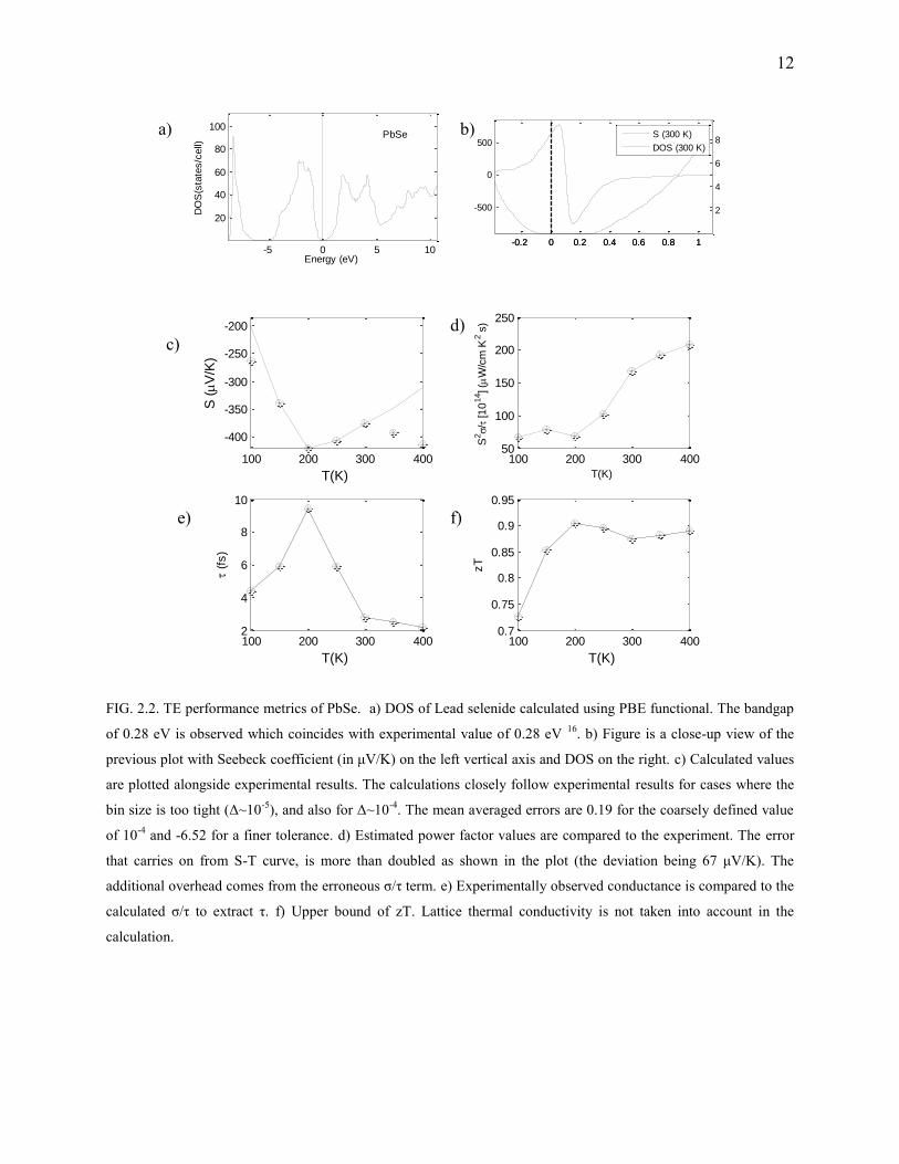
FIG. 2.2. TE performance metrics of PbSe. a) DOS of Lead selenide calculated using PBE functional. The bandgap
of 0.28 eV is observed which coincides with experimental value of 0.28 eV 16. b) Figure is a close-up view of the
previous plot with Seebeck coefficient (in μV/K) on the left vertical axis and DOS on the right. c) Calculated values
are plotted alongside experimental results. The calculations closely follow experimental results for cases where the
bin size is too tight (Δ~10-5
), and also for Δ~10-4. The mean averaged errors are 0.19 for the coarsely defined value
of 10-4 and -6.52 for a finer tolerance. d) Estimated power factor values are compared to the experiment. The error
that carries on from S-T curve, is more than doubled as shown in the plot (the deviation being 67 μV/K). The
additional overhead comes from the erroneous σ/τ term. e) Experimentally observed conductance is compared to the
calculated σ/τ to extract τ. f) Upper bound of zT. Lattice thermal conductivity is not taken into account in the
calculation.
100 200 300 400
-400
-350
-300
-250
-200
T(K)
S (V
/K)
100 200 300 40050
100
150
200
250
T(K)S
2/
[1
014] (
W/c
m K
2 s
)
100 200 300 4002
4
6
8
10
T(K)
(f
s)
log10
Nd(/cm3)=18
100 200 300 4000.7
0.75
0.8
0.85
0.9
0.95
T(K)
zT
a) b)
c) d)
e) f)

13
FIG. 2.3. DOS plot of PbTe. PBE functional is used to calculate the electronic structure (above). The estimated
bandgap is close to 0.35 eV as compared to the experimental15 0.3 eV.
FIG. 2.4. Experimental PbTe S vs T fit. As with the selenide version, the S-T curves in PbTe are also insensitive to
a considerable change in the levels of tolerance. The doping concentration is estimated to be around: 1.38E019.
-10 -5 0 5 10
100
200
300
400
PbTe
E-Ef (eV)
DO
S(s
tate
s/c
ell)
300 400 500 600 700
-300
-250
-200
-150
T(K)
S (V
/K)
log10
Nd(/cm3)=19
err nth place:18
err nth place:17
exp.
14
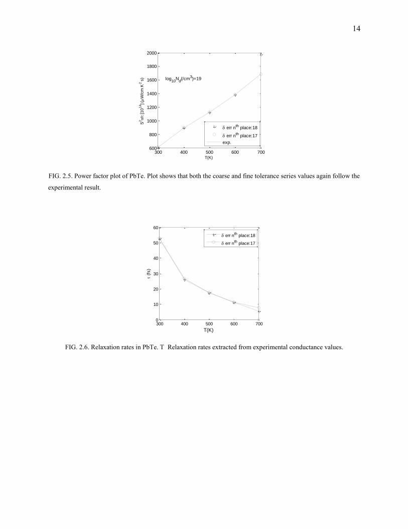
FIG. 2.5. Power factor plot of PbTe. Plot shows that both the coarse and fine tolerance series values again follow the
experimental result.
FIG. 2.6. Relaxation rates in PbTe. T Relaxation rates extracted from experimental conductance values.
300 400 500 600 700600
800
1000
1200
1400
1600
1800
2000
T(K)
S2/
[1
014] (
W/c
m K
2 s
)
log10
Nd(/cm3)=19
err nth place:18
err nth place:17
exp.
300 400 500 600 7000
10
20
30
40
50
60
T(K)
(f
s)
err nth place:18
err nth place:17
15
FIG. 2.7. PbTe zT plot. kl-th is assumed to be zero. Hence, from now on, any mention of zT is the maximum practical
one can have (ref. Chapter I-alloying) without changing the electronic structure.
FIG. 2.8. PbTe S-T curves for various doping concentrations. A negative value in the doping concentration implies
n-type dopant.
300 400 500 600 700
0.65
0.7
0.75
0.8
0.85
T(K)
zT
err nth place:18
err nth place:17
0 100 200 300 400 500 600 700 800-600
-400
-200
0
200
400
600
800
T(K)
S (
V/K
)
1020 1019 1018 -1019 -1018 -10E17
16
FIG. 2.9. PbTe pf -T plot for different doping levels. The power factor on the doped n-side has a lower slope owing
to the distance of the conduction band edge from the Fermi level.
FIG. 2.10. PbTe zT-T plot for different doping concentrations. Performance is better at lower doping levels.
The rationale is as follows: the very crude assumption of bandgap independence on
temperature fails in this casea. Decrease in bandgap proves more costly (in transport) than
increasing it by the same amount (as it is apparent from the simple models presented in the
earlier chapter). PbSe is very sensitive to temperature dependence on bandgap14.
a Rigid band model was assumed for all BTE calculations
0 200 400 600 800-2000
0
2000
4000
6000
8000
10000
12000
T(K)
S2/
[1
014] (
W/c
m K
2 s
)
1020
1019
1018
-1019
-1018
-10E17
0 200 400 600 800-1
-0.5
0
0.5
1
T(K)
zT
1020
1019
1018
-1019
-1018
-10E17

17
A zeroth order estimate: large atomic ratio differences lead to higher amplitude of phonon
scatteringb,18 (Mass %Δ – PbSe: 0.37, PbTe: 0.67) which implies the bandgap is robust to
temperature changes in PbTe.
β-Ag2Se
β-Ag2Se is known for its low lattice thermal conductivity (~5mW cm-1 K), low resistance (5E(-4)
ohm cm-1) and a reasonably good Seebeck coefficient19 (150 μV/K). Bandgap of Ag2Se was
estimated to be 70 meV (Fig. 2.11) as compared to the experimental value14,20 of 120 meV.
Narrow-band semiconductors (Ag2Se, Half-heusler) often are victims of the infirmities of DFT.
Narrow-band gaps are underestimated as well! The degree of error is critical in determining
Seebeck coefficients (Fig.2.12). Wide bandgap semiconductors show minimal deviation (as
apparent from the two-band models (a and c)) for the percentage change in the Seebeck
coefficient is mild. Further, relaxation time and zT values are extracted from the experimental fit
(Fig. 2.13-2.14).
FIG. 2.11. DOS plot of Ag2Se crystal. The electronic states are minimal but exist right at the Fermi level making
Ag2Se a “bad”-insulator.
b Disorder scattering is prominent in elements that have large atomic mass differences. Short wavelength phonons
are scattered and hence several modes are “annihilated”. Non-availability of phonon modes reduces e-ph scattering.
-10 -5 0 50
200
400
600 Ag2Se
Energy (eV)
DO
S(s
tate
s/c
ell)

18
FIG. 2.12. Experimental Ag2Se S-T fits. The doping concentration is estimated to be around 18.6E19.
FIG. 2.13. Ag2Se pf-T and relaxation time plots. The results obtained from transport calculations are fit to
experiment. Discrepancies in the fit are a result of phase change at 160K. Misfit of data is a diagnostic of
a wrong calculation, observation of which is used as a tool to estimate the Curie temperature in Chapter III.
100 150 200 250 300100
200
300
400
500
600
700
800
900
1000
T(K)
S2/
[1
014] (
W/c
m K
2 s
)
log10
Nd(/cm3)=19
err nth place:17
err nth place:18
exp.
100 150 200 25015
16
17
18
19
20
21
T(K)
(f
s)
err nth place:19
err nth place:18
19
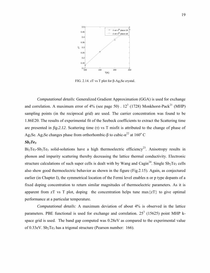
FIG. 2.14. zT vs T plot for β-Ag2Se crystal.
Computational details: Generalized Gradient Approximation (GGA) is used for exchange
and correlation. A maximum error of 4% (see page 50) . 123 (1728) Monkhorst-Pack21 (MHP)
sampling points (in the reciprocal grid) are used. The carrier concentration was found to be
1.86E20. The results of experimental fit of the Seebeck coefficients to extract the Scattering time
are presented in fig.2.12. Scattering time (τ) vs T misfit is attributed to the change of phase of
Ag2Se. Ag2Se changes phase from orthorhombic-β to cubic-α22 at 160o C
Sb2Te3
Bi2Te3-Sb2Te3 solid-solutions have a high thermoelectric efficiency23. Anisotropy results in
phonon and impurity scattering thereby decreasing the lattice thermal conductivity. Electronic
structure calculations of such super cells is dealt with by Wang and Cagin24. Single Sb2Te3 cells
also show good thermoelectric behavior as shown in the figure (Fig.2.15). Again, as conjectured
earlier (in Chapter I), the symmetrical location of the Fermi level enables n or p type dopants of a
fixed doping concentration to return similar magnitudes of thermoelectric parameters. As it is
apparent from zT vs T plot, doping the concentration helps tune max{zT} to give optimal
performance at a particular temperature.
Computational details: A maximum deviation of about 4% is observed in the lattice
parameters. PBE functional is used for exchange and correlation. 253 (15625) point MHP k-
space grid is used. The band gap computed was 0.28eV as compared to the experimental value
of 0.33eV. Sb2Te3 has a trigonal structure (Pearson number: 166).
100 150 200 2500.1
0.15
0.2
0.25
0.3
0.35
0.4
0.45
0.5
T(K)
zT
err nth place:19
err nth place:18

20
FIG. 2.15. TE performance metrics of Sb2Te3. a)DOS plot, b) Seebeck coefficient c) power factor d) zT of Sb2Te3.
2.2 Half-Heuslers
Half-heuslers(HH) are Heusler structures with half atoms missing (Fig.2.16). Valence electron
count (VEC) determines the electronic structure of Heusler25 and HH structures26. VEC count
-10 -5 0 5 10
50
100
150
200 Sb2Te
3
Energy (eV)
DO
S(s
tate
s/c
ell)
0 200 400 600 800 1000-400
-300
-200
-100
0
100
200
300
400
T(K)
S (
V/K
)
1019
1018
1017
-1019
-1018
-10E17
0 200 400 600 800 1000-3000
-2000
-1000
0
1000
2000
3000
T(K)
S2/
[1
014] (
W/c
m K
2 s
)
1019
1018
1017
-1019
-1018
-10E17
0 200 400 600 800 1000-1
-0.5
0
0.5
1
T(K)
zT
1019 1018 1017 -1019 -1018 -10E17
a)
b)
c)
d)

21
FIG. 2.16. Summary of lattice parameters, computational parameters, and band gaps in Half-Heuslers.
ZrNiSn
Experimental
Structure: cubic
[a b c]: 6.11
Bandgap: 0.1227
DFT (L(S)DA+U)
Energy Cutoff: 450
[a b c]: 6.2
Bandgap: 0.18 eV
K-Points: 17576
Maximum zT: 0.7 around
200K
Atoms: 2
Niobium Ferrous
Antimonide(NbFeSb)
Experimental
Structure:cubic
[a b c]: 5.96
Bandgap:(-)
DFT(LDA)
Energy Cutoff:400
[a b c]: 5.96
Bandgap: 0.075 eV
K-Points: 5832
Maximum zT: 1.14 below
400K
Atoms: 3
CoSbTi
Experimental
Structure: cubic
[a b c]: 5.88
Bandgap: 0.9528
DFT(PBE)
Energy Cutoff: 450
[a b c]: 5.89
Bandgap: 0.98 eV
K-Points: 13824
Maximum zT: 0.8 at over
1000K
Atoms: 12
Lanthanum Aluminium
Silicide (LaAlSi)
Experimental
Structure: cubic
[a b c]: 5.94
Bandgap: (-)
DFT(GGA)
Energy Cutoff:450
[a bc ]: 5.94
Bandgap: 0.39 eV
K-Points: 8000
Maximum zT: 0.8-0.7
around 200K
Atoms: 3
22
of 18 implies existence of bandgap in HH29. HH are usually narrow bandgap semiconductorsc
that have moderate zT at high temperatures30. The important contributing factor to this
“moderateness” is the thermal-conductivity (for eg. NiSnZr has k close to 10 W/m·K). But, their
thermal conductivities are obviously lower than their Heusler counterparts. Tailoring the crystal
could improve the thermal conductivity. For eg. in NiSnZr, Zr is replaced by a heavier Hf31
and the thermoelectric conductivity was halved. The maximum zT in NiSnZr was found to be 0.7
which also happens to be an experimental prediction31. Most HH are n-type. It is still a challenge
to find their intrinsic p-type and Si-Ge like alter ego. Asymmetry in the position of the Fermi
level in the case of LaAlSi and CoSbTi implies they are a natural p-type alloys. In this study,
four HH alloys were studied: i) CoSbTi (Fig.2.17) ii) NiSnZr (Fig. 2.18-2.20) iii) LaAlSi (Fig.
2.21) and iv)NbFeSb (Fig.2.22-2.24).
An ideal thermoelectric not only has a high zT, but work efficiently for a broad
temperature range. While three of the four observed structures performed well at 200 K (with zT
~ 0.75), counter intuitive to the generalized perception of zT in HH, NbFeSb has a high zT and
behaves as a good thermoelectric over a wide temperature range and for a given doping
concentration.
CoSbTi
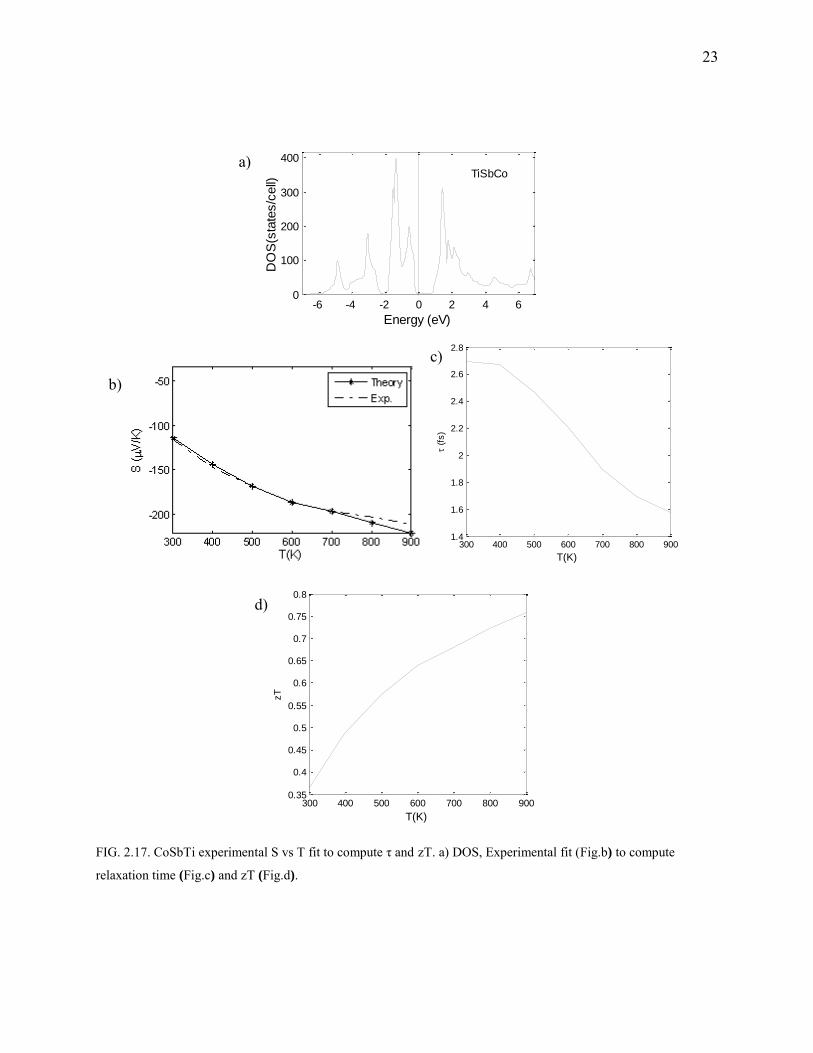
From the functional form of the Seebeck coefficient, it is apparent that sharp DOS would lead to
high S. These ternary inter-metallic structures resemble the MgAgAs cubic types. The transport
coefficients of CoSbTi are fit to experiments (Fig.2.17). The doping concentration is estimated as
1.03E20 /cm3. The bandgap was found to be : 0.98 eV (exp.:0.95). PBE functional was used for
both exchange and correlation. The lattice parameters are almost the same as the experiment
(deviation of 0.002%).
c Take the case of NiSnZr, the bandgap is thanks to the hybridization of the d-shell electrons of Ni and p-electrons of
Sn , and also contribution due to exchange splitting.
23
FIG. 2.17. CoSbTi experimental S vs T fit to compute τ and zT. a) DOS, Experimental fit (Fig.b) to compute
relaxation time (Fig.c) and zT (Fig.d).
-6 -4 -2 0 2 4 60
100
200
300
400
TiSbCo
Energy (eV)
DO
S(s
tate
s/c
ell)
300 400 500 600 700 800 9001.4
1.6
1.8
2
2.2
2.4
2.6
2.8
T(K)
(f
s)
log10
Nd(/cm3)=23
300 400 500 600 700 800 9000.35
0.4
0.45
0.5
0.55
0.6
0.65
0.7
0.75
0.8
T(K)
zT
a)
b)
c)
d)
24
NiSnZr
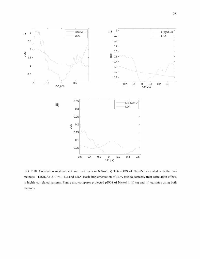
NiSnZr is our first case where the use of LDA along with a fudge-factor “U”, is necessary to
prevent Mott-insulator7, 32 behavior (Fig.2.18). The approximate exchange-correlation functional,
no doubt, gives reasonable results for ground state energies, but fails in spelling out the proper
electronic structure. Metallic behavior of the Half-filled d-shells is the prime reason for such an
observation. In such cases, d-d Coulombic energies have to be taken into account and if one adds
such a correction, the metallic behavior disappears. Is there a reasonable value of U to be added?
Yes! “U”, obviously depends on the orbital occupancy which means that the half-filled orbitals
have less magnitude of U than the quarter-filled ones. One could make an educated guess and
sweep U to match the lattice parameters or the electronic bandgap, OR a single-shot calculation
needs the value of U be obtained from XPSd,e,f. It is apparent from Fig.2.20 that NiSnZr has a
satisfactory max{zT} of 0.7 which agrees with the experimental prediction31 which predicts
maximum zT to be around 0.7.
Computational details: The L(S)DAU parameters used are: U=7.52 and J=0.65. MHP
grid of 263 was used. The deviation from experimental lattice parameters was close to 1%.
d This exercise doesn’t guarantee exact lattice parameters as there are other shells that suffer from the lack of a
better exchange-correlation functional. e Ref. [31] deals with the extraction of U from XPS binding energies. In general, it is the effective (U-J) that needs
to be corrected, J being the exchange correction which also depends on the occupancy since the exchange and
correlation are a lumped unit in GGA/LDA. f Occupancies needn’t always be whole numbers as it would be shown in Chapter III, the electron occupancies may
even assume fractional values owing to hybridization of a particular state.
25
FIG. 2.18. Correlation mistreatment and its effects in NiSnZr. i) Total-DOS of NiSnZr calculated with the two
methods – L(S)DA+U (U=7.5, J=0.65) and LDA. Basic implementation of LDA fails to correctly treat correlation effects
in highly correlated systems. Figure also compares projected pDOS of Nickel in ii) t2g and iii) eg states using both
methods.
-0.2 -0.1 0 0.1 0.2 0.3
0.1
0.2
0.3
0.4
0.5
0.6
0.7
0.8
0.9
1
E-Ef(eV)
DO
S
L(S)DA+U
LDA
-1 -0.5 0 0.5
0.5
1
1.5
2
2.5
3
E-Ef(eV)
DO
S
L(S)DA+U
LDA
-0.6 -0.4 -0.2 0 0.2 0.4 0.6
0.05
0.1
0.15
0.2
0.25
0.3
0.35
E-Ef(eV)
DO
S
L(S)DA+U
LDA
i) ii)
iii)

26
FIG. 2.19. NiSnZr S-T and pf-T curves. a) Seebeck coefficient and b) power factor plots of NiSnZr.
0 200 400 600 800 1000-200
-150
-100
-50
0
50
100
150
200
250
T(K)
S (
V/K
)
-2.17*1023
-2.172*1023
-2.174*1023
-2.176*1023
-2.178*1023
-2.18*1023
0 200 400 600 800 10000
500
1000
1500
2000
2500
3000
3500
4000
4500
5000
T(K)
S2/
[1
014] (
W/c
m K
2 s
)
-2.17*1023
-2.172*1023
-2.174*1023
-2.176*1023
-2.178*1023
-2.18*1023
a)
b)
27
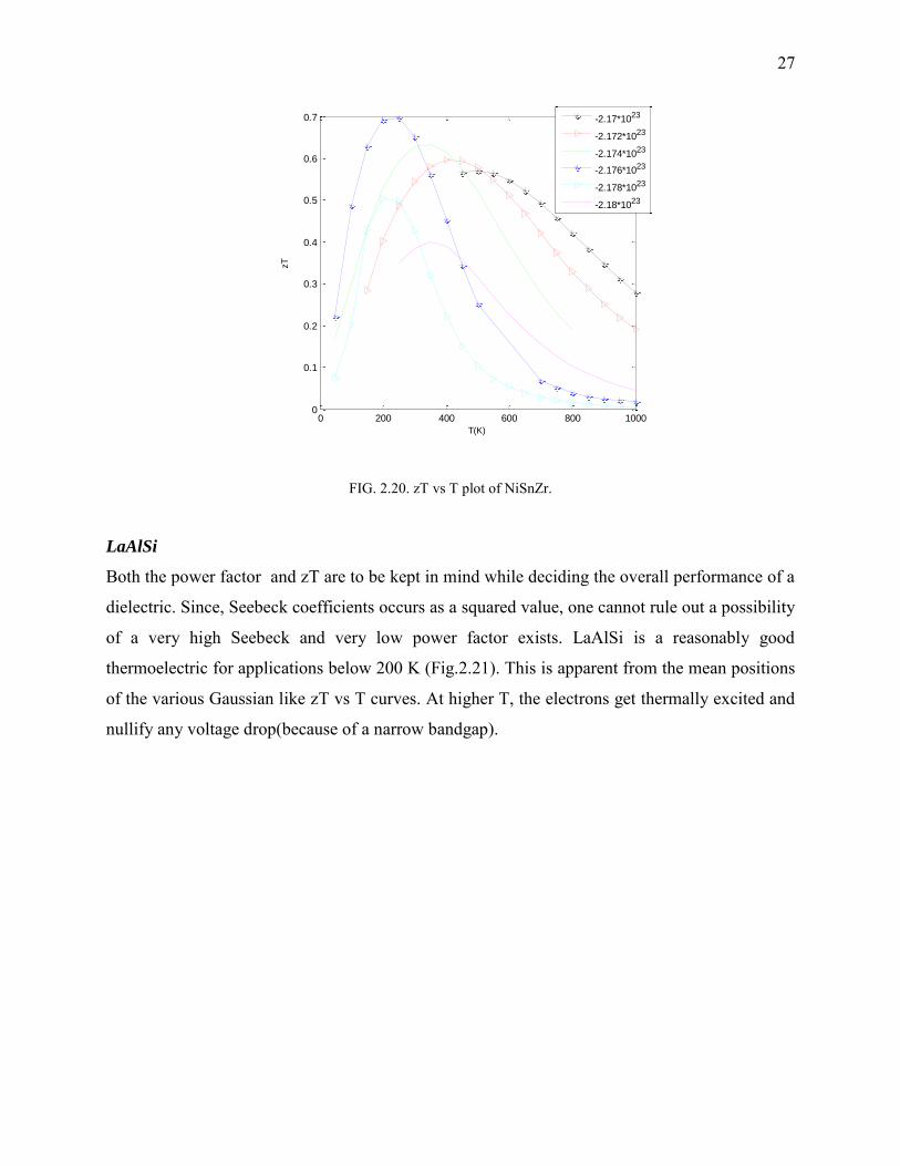
FIG. 2.20. zT vs T plot of NiSnZr.
LaAlSi
Both the power factor and zT are to be kept in mind while deciding the overall performance of a
dielectric. Since, Seebeck coefficients occurs as a squared value, one cannot rule out a possibility
of a very high Seebeck and very low power factor exists. LaAlSi is a reasonably good
thermoelectric for applications below 200 K (Fig.2.21). This is apparent from the mean positions
of the various Gaussian like zT vs T curves. At higher T, the electrons get thermally excited and
nullify any voltage drop(because of a narrow bandgap).
0 200 400 600 800 10000
0.1
0.2
0.3
0.4
0.5
0.6
0.7
T(K)
zT
-2.17*1023
-2.172*1023
-2.174*1023
-2.176*1023
-2.178*1023
-2.18*1023

28
FIG. 2.21. TE performance metrics of LiAlSi. a) DOS , b) Seebeck coefficient , c) power factor and d) zT plots of
LiAlSi.
-6 -4 -2 0 2 4 6
20
40
60
80 LaAlSi
Energy (eV)
DO
S(s
tate
s/c
ell)
0 200 400 600 800 1000-300
-200
-100
0
100
200
300
400
T(K)
S (
V/K
)
1E18
1E19
1E20
-1E18
-1E19
-1E20
0 200 400 600 800 10000
500
1000
1500
2000
2500
T(K)
S2/
[1
014] (
W/c
m K
2 s
)
1E18
1E19
1E20
-1E18
-1E19
-1E20
0 200 400 600 800 10000
0.1
0.2
0.3
0.4
0.5
0.6
0.7
0.8
0.9
T(K)
zT
1E18
1E19
1E20
-1E18
-1E19
-1E20
a)
b)
c)
d)
29
NbFeSb
Suprisingly, NbFeSb shows a good thermoelectric behavior for temperatures below 600K
(Fig.2.23-2.24). There was minimal deviation in the calculated structural parameters when
compared to the experimental ones obtained from ICSD. The bandgap was found to be 0.075 eV
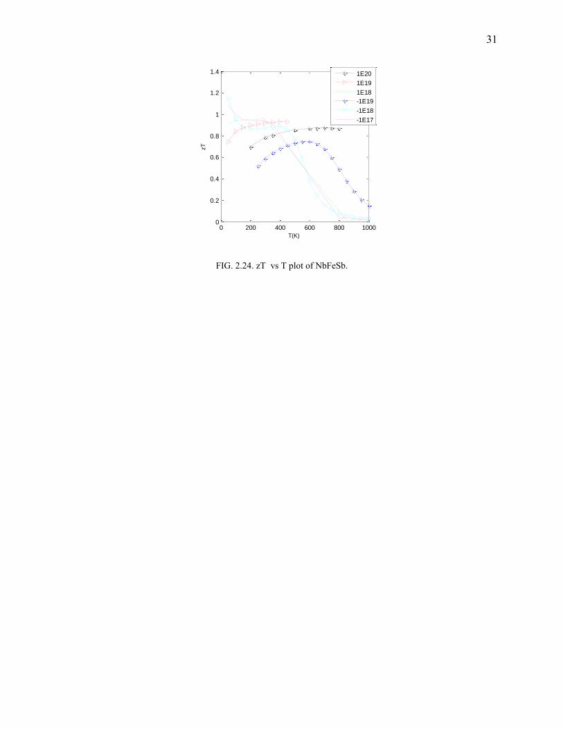
(Fig.2.22). A maximum zT was found to be 1.14. Bandgap being small, it is possible for even the
faintest of temperature gradients to populate the conduction band (which has a sharp band edge).
Since the conduction band electrons are massive (from the DOS) and delocalized, it possibly
develops reasonable potential drop (as is it proportional to the effective mass) and also has high-
conductivity.
Computational details: There was minimal deviation between the experimental and the
computed lattice parameters. LDA was used for both the exchange and correlation functional.
183 MHP grid was used from an SCF calculation which followed a 83 MHP relaxationg.
Statement without proof: The difference between computed lattice parameters and the
experimental values is minimal if one uses a primitive cell representation instead of the
supercell.
FIG. 2.22. DOS plot of NbFeSb.
g Prior to calculating the SCF data values, all structures were checked for convergence (1 meV) on the k-points and
the total energy.
-0.15 -0.1 -0.05 0 0.05 0.1
100
200
300
E-Ef
DO
S
30
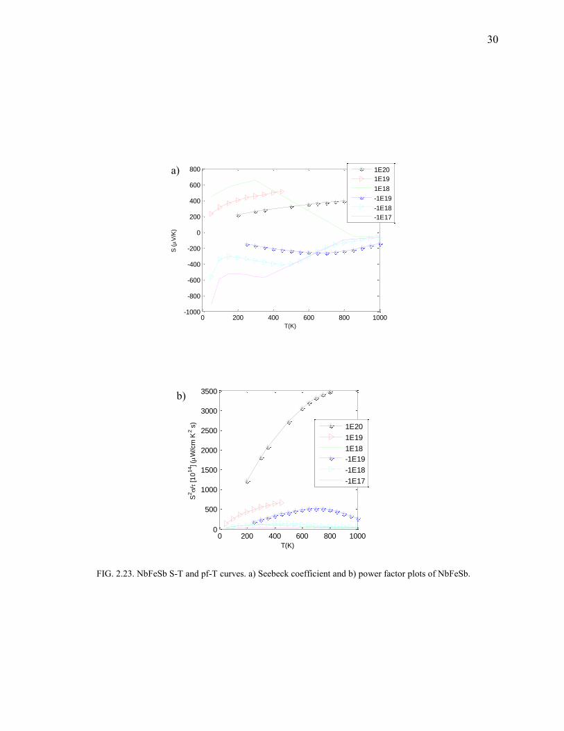
FIG. 2.23. NbFeSb S-T and pf-T curves. a) Seebeck coefficient and b) power factor plots of NbFeSb.
0 200 400 600 800 1000-1000
-800
-600
-400
-200
0
200
400
600
800
T(K)
S (
V/K
)
1E20
1E19
1E18
-1E19
-1E18
-1E17
0 200 400 600 800 10000
500
1000
1500
2000
2500
3000
3500
T(K)
S2/
[1
014] (
W/c
m K
2 s
)
1E20
1E19
1E18
-1E19
-1E18
-1E17
a)
b)
31
FIG. 2.24. zT vs T plot of NbFeSb.
0 200 400 600 800 10000
0.2
0.4
0.6
0.8
1
1.2
1.4
T(K)
zT
1E20
1E19
1E18
-1E19
-1E18
-1E17
32
2.3 Perovskites
Structures having ABO3 arrangement (Fig.2.25) with A atoms sitting on the corners of the cube,
B at the BCC and O’s occupying the FCC positions, are classified as Perovskites. Being oxides,
they behave as good dielectrics and have potential applications as high-zT-thermoelectrics.
Perovskite structures usually have electrons with a large effective mass (close to 10m0)33 which
is a direct indication of its high Seebeck coefficient. The thermal conductivities of these ceramics
are usually very high (for BaTiO3(BTO)-8.5 W m-1 K-1 and for SrTiO3(STO)~10 W m-1 K-1).
However, like in the Si-Ge alloys, alloys of solid-solutions of BTO and STO have disorder
scattering, thereby tremendously reducing the value of thermal conductivity. Since we are
interested in just the electronic contribution, we neglect kl assuming it to be minimum.
Lanthanum Cobaltate (also a Perovskite)-dealt as a special case in Chapter III, shows a peculiar
behavior. There are multiple spin phases of LaCoO3. Estimating Seebeck coefficient could be
difficult when phase transitions occur. We, however, outline a simple procedure to compute the
Curie temperature and also the thermoelectric parameters, thereof. The structure CaSiO3 shows a
good room temperature thermoelectric behavior with a zTmax of almost unity.
STO and BTO
As with the case of NiSnZr, half-filled d-shells suffer from drastic reduction in bandgaps. We
used L(S)DA+U, STO:U=4.844,J=0.92 and BTO:U=4.71,J=0.90 (values obtained by XPS
comparison) to include strong correlation effect and obtain bandgap as shown in Fig.2.26. In the
case of STO, the doping concentration is high (0.6E21) due to the unconventional experiment
employing a p-type dopant34. This configuration fares well at 1000 K (Fig.2.27-2.29; Fig.2.30-
Fig.2.31) where a zTmax with S=305 μV/K, is found to be around 0.85.
Computational details: A 253(15625) MHP reciprocal space grid is used. PBE is used
for xc. The band gap was found to be about 3.2 eV matching the experimental value.
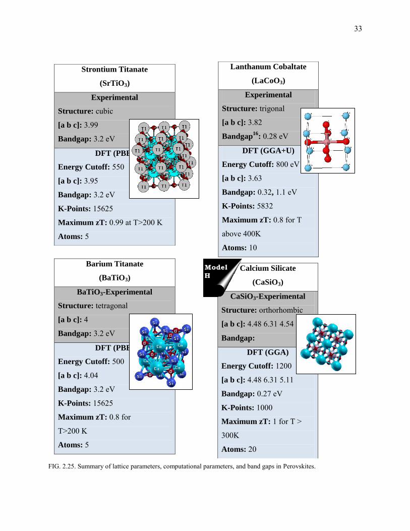
33
FIG. 2.25. Summary of lattice parameters, computational parameters, and band gaps in Perovskites.
Lanthanum Cobaltate
(LaCoO3)
Experimental
Structure: trigonal
[a b c]: 3.82
Bandgap16
: 0.28 eV
DFT (GGA+U)
Energy Cutoff: 800 eV
[a b c]: 3.63
Bandgap: 0.32, 1.1 eV
K-Points: 5832
Maximum zT: 0.8 for T
above 400K
Atoms: 10
Strontium Titanate
(SrTiO3)
Experimental
Structure: cubic
[a b c]: 3.99
Bandgap: 3.2 eV
DFT (PBE)
Energy Cutoff: 550
[a b c]: 3.95
Bandgap: 3.2 eV
K-Points: 15625
Maximum zT: 0.99 at T>200 K
Atoms: 5
Barium Titanate
(BaTiO3)
BaTiO3-Experimental
Structure: tetragonal
[a b c]: 4
Bandgap: 3.2 eV
DFT (PBE)
Energy Cutoff: 500
[a b c]: 4.04
Bandgap: 3.2 eV
K-Points: 15625
Maximum zT: 0.8 for
T>200 K
Atoms: 5
Calcium Silicate
(CaSiO3)
CaSiO3-Experimental
Structure: orthorhombic
[a b c]: 4.48 6.31 4.54
Bandgap:
DFT (GGA)
Energy Cutoff: 1200
[a b c]: 4.48 6.31 5.11
Bandgap: 0.27 eV
K-Points: 1000
Maximum zT: 1 for T >
300K
Atoms: 20

34
FIG. 2.26. STO electronic structure and experimental S-T fits to extract τ and zT. DOS [fig.a] , partial DOS (LDA,
L(S)DAU) [fig.b], relaxation time [fig.c] vs temperature, zT [fig.d], Seebeck coefficient [fig.e] fit to experiment.
-25 -20 -15 -10 -5 0 5 100
5
10SrTiO
3
Energy (eV)
DO
S
-4 -2 0 2 40
1
2
3
E-Ef(eV)
pD
OS
(Ti)
L(S)DA+U
LDA
500 600 700 800 900 10000.2
0.21
0.22
0.23
0.24
0.25
T(K)
(f
s)
log10
Nd(/cm3)=21
500 600 700 800 900 1000
250
300
350
T(K)
S (V
/K)
log10
Nd(/cm3)=21
Theory
Exp.
500 600 700 800 900 10000.65
0.7
0.75
0.8
0.85
0.9
T(K)
zT
a)
b)
c)
e)
d)
35
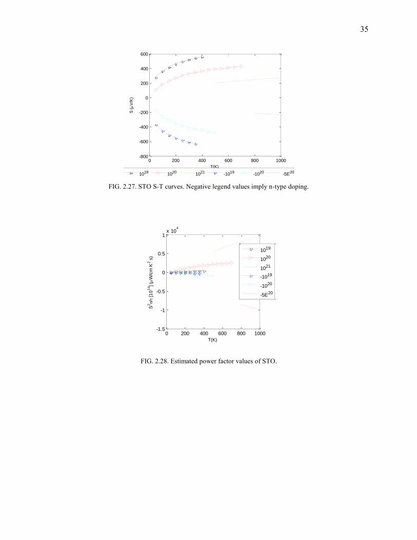
FIG. 2.27. STO S-T curves. Negative legend values imply n-type doping.
FIG. 2.28. Estimated power factor values of STO.
0 200 400 600 800 1000-800
-600
-400
-200
0
200
400
600
T(K)
S (
V/K
)
1019 1020 1021 -1019 -1020 -5E20
0 200 400 600 800 1000-1.5
-1
-0.5
0
0.5
1x 10
4
T(K)
S2/
[1
014] (
W/c
m K
2 s
)
1019
1020
1021
-1019
-1020
-5E20
36
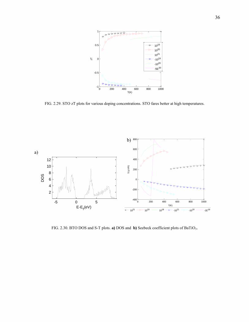
FIG. 2.29. STO zT plots for various doping concentrations. STO fares better at high temperatures.
FIG. 2.30. BTO DOS and S-T plots. a) DOS and b) Seebeck coefficient plots of BaTiO3.
0 200 400 600 800 1000-1
-0.5
0
0.5
1
T(K)zT
1019
1020
1021
-1019
-1020
-5E20
-5 0 5
2
4
6
8
10
12
E-Ef(eV)
DO
S
0 200 400 600 800 1000-400
-200
0
200
400
600
800
T(K)
S (
V/K
)
1021 1019 1018 -1021 -1019 -1E18
a)
b)

37
FIG. 2.31. BTO pf-T and zT plots for various doping concentrations. a) power factor and b) zT plots of BaTiO3.
CaSiO3
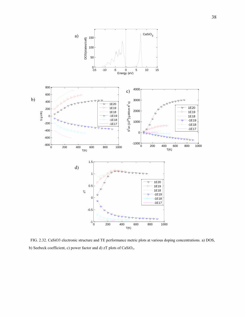
For the same concentration, (ref. Fig.2.32), p-type CaSiO3 fares better than the n-doped structure.
It boasts of a good power factor and a moderate-to-good Seebeck coefficient. The maximum zT
was found to be 1.05 (Fig.2.32) at room temperature and was found to be independent of carrier
concentration in the p-type CaSiO3. Clearly, since the conduction band-edge implies a lighter
effective mass, though the mobility is high, it is prone to scattering. No experimental data on the
thermal conductivity of the perovskite phase of CaSiO3 is available. But oxygen rich Perovskite
structures have a good thermal conductivity.
0 200 400 600 800 1000-1
-0.5
0
0.5
1
T(K)
zT
1021
1019
1018
-1021
-1019
-1E18
0 200 400 600 800 1000-1.5
-1
-0.5
0
0.5
1
1.5x 10
4
T(K)
S2/
[1
014] (
W/c
m K
2 s
)
1021 1019 1018 -1021 -1019 -1E18
a) b)
38
FIG. 2.32. CaSiO3 electronic structure and TE performance metric plots at various doping concentrations. a) DOS,
b) Seebeck coefficient, c) power factor and d) zT plots of CaSiO3.
-15 -10 -5 0 5 10 150
50
100
150CaSiO
3
Energy (eV)
DO
S(s
tate
s/c
ell)
0 200 400 600 800 1000-800
-600
-400
-200
0
200
400
600
800
T(K)
S (V
/K)
1E20
1E19
1E18
-1E19
-1E18
-1E17
0 200 400 600 800 1000-1000
0
1000
2000
3000
4000
T(K)
S2/
[1
014] (
W/c
m K
2 s
)
1E20
1E19
1E18
-1E19
-1E18
-1E17
0 200 400 600 800 1000-1
-0.5
0
0.5
1
1.5
T(K)
zT
1E20
1E19
1E18
-1E19
-1E18
-1E17
a)
b)
c)
d)
39
2.4 Assorted Class of Thermoelectrics
Please refer Fig.2.33 for a list of crystal structures under this category and their TE performance.
ZnO
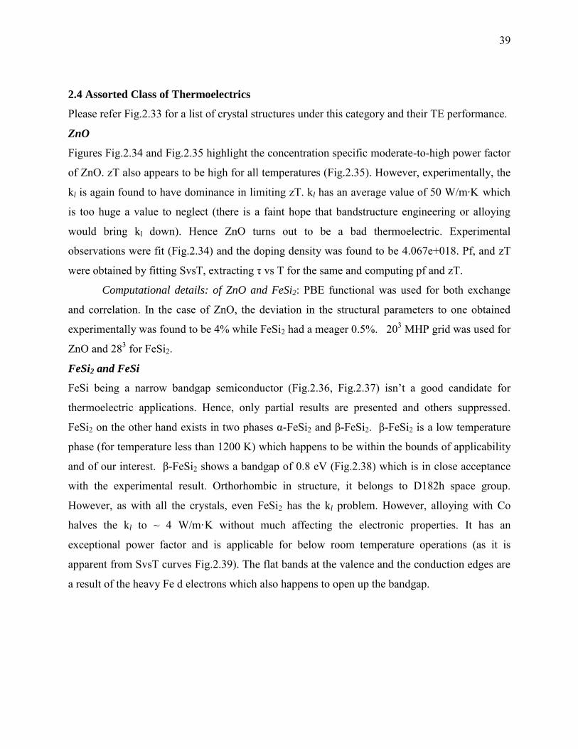
Figures Fig.2.34 and Fig.2.35 highlight the concentration specific moderate-to-high power factor
of ZnO. zT also appears to be high for all temperatures (Fig.2.35). However, experimentally, the
kl is again found to have dominance in limiting zT. kl has an average value of 50 W/m·K which
is too huge a value to neglect (there is a faint hope that bandstructure engineering or alloying
would bring kl down). Hence ZnO turns out to be a bad thermoelectric. Experimental
observations were fit (Fig.2.34) and the doping density was found to be 4.067e+018. Pf, and zT
were obtained by fitting SvsT, extracting τ vs T for the same and computing pf and zT.
Computational details: of ZnO and FeSi2: PBE functional was used for both exchange
and correlation. In the case of ZnO, the deviation in the structural parameters to one obtained
experimentally was found to be 4% while FeSi2 had a meager 0.5%. 203 MHP grid was used for
ZnO and 283 for FeSi2.
FeSi2 and FeSi
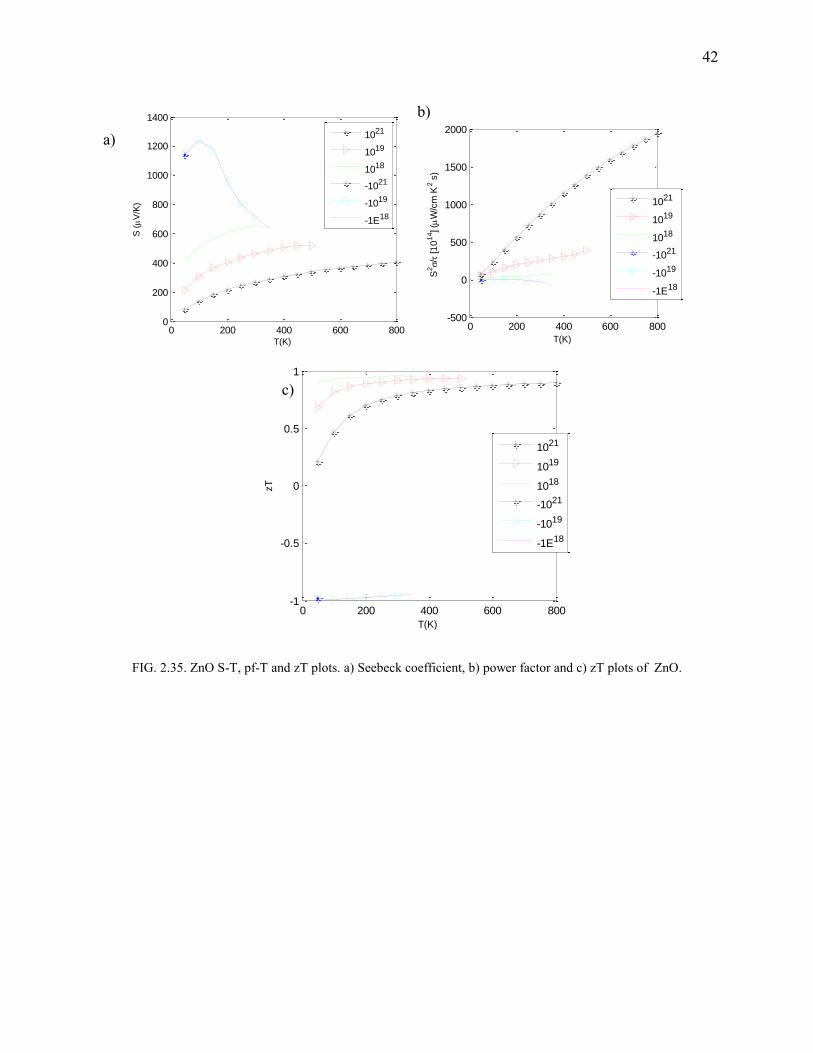
FeSi being a narrow bandgap semiconductor (Fig.2.36, Fig.2.37) isn’t a good candidate for
thermoelectric applications. Hence, only partial results are presented and others suppressed.
FeSi2 on the other hand exists in two phases α-FeSi2 and β-FeSi2. β-FeSi2 is a low temperature
phase (for temperature less than 1200 K) which happens to be within the bounds of applicability
and of our interest. β-FeSi2 shows a bandgap of 0.8 eV (Fig.2.38) which is in close acceptance
with the experimental result. Orthorhombic in structure, it belongs to D182h space group.
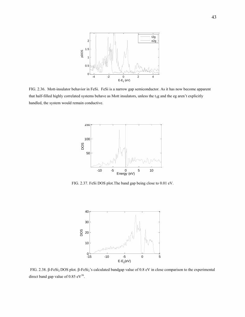
However, as with all the crystals, even FeSi2 has the kl problem. However, alloying with Co
halves the kl to ~ 4 W/m·K without much affecting the electronic properties. It has an
exceptional power factor and is applicable for below room temperature operations (as it is
apparent from SvsT curves Fig.2.39). The flat bands at the valence and the conduction edges are
a result of the heavy Fe d electrons which also happens to open up the bandgap.

40
FIG. 2.33. Summary of lattice parameters, computational parameters, and band gaps of the assorted class of
thermoelectrics.
FeSi2
Experimental
Structure: orthorhombic
[a b c]: -6.23 6.23 7.81
Bandgap16
: 0.78 eV
DFT(PBE)
Energy Cutoff: 400 eV
[a b c]:6.187 6.187 7.688
Bandgap35
: 0.8 eV
K-Points: 21952
Maximum zT: 1 above
200K
Atoms: 24
FeSi
Experimental
Structure: cubic
[a b c]: 4.45
Bandgap16
: 0.28 eV
DFT(PBE)
Energy Cutoff: 400 eV
[a b c]: 4.45
Bandgap: 0.1 eV
K-Points: 15625
Maximum zT: 0.9 at
150K
Atoms: 8
Zinc Oxide
(ZnO)
Experimental
Structure: hexagonal
[a b c]: 3.25 3.25 5.20
Bandgap16
: 3.1 eV
DFT(PBE)
Energy Cutoff: 300 eV
[a b c]: 3.28 3.28 5.32
Bandgap: 3.2 eV
K-Points: 8000
Maximum zT: 1 above
200K
Atoms: 4

41
FIG. 2.34. Electronic structure and TE performance plots of ZnO. a) DOS , b) Seebeck coefficient, c) power factor
and d) zT plots of ZnO fit to experiments. The doping concentration was found to be -4E18.
-6 -4 -2 0 2 4 6
50
100
150
200
250
300ZnO
Energy (eV)
DO
S(s
tate
s/c
ell)
300 400 500 600 700 800
-220
-200
-180
-160
-140
T(K)
S (V
/K)
log10
Nd(/cm3)=19
err nth place:17
err nth place:18
exp.
300 400 500 600 700 800100
150
200
250
300
350
400
450
500
T(K)
S2/
[1
014] (
W/c
m K
2 s
)
log10
Nd(/cm3)=19 err nth place:17
err nth place:18
exp.
300 400 500 600 700 8000.68
0.7
0.72
0.74
0.76
0.78
0.8
0.82
T(K)
zT
err nth place:17
err nth place:18
a)
b)
c) d)
42
FIG. 2.35. ZnO S-T, pf-T and zT plots. a) Seebeck coefficient, b) power factor and c) zT plots of ZnO.
0 200 400 600 8000
200
400
600
800
1000
1200
1400
T(K)
S (
V/K
)
1021
1019
1018
-1021
-1019
-1E18
0 200 400 600 800-500
0
500
1000
1500
2000
T(K)
S2/
[1
014] (
W/c
m K
2 s
)
1021
1019
1018
-1021
-1019
-1E18
0 200 400 600 800-1
-0.5
0
0.5
1
T(K)
zT
1021
1019
1018
-1021
-1019
-1E18
a)
b)
c)
43
FIG. 2.36. Mott-insulator behavior in FeSi. FeSi is a narrow gap semiconductor. As it has now become apparent
that half-filled highly correlated systems behave as Mott insulators, unless the t2g and the eg aren’t explicitly
handled, the system would remain conductive.
FIG. 2.37. FeSi DOS plot.The band gap being close to 0.01 eV.
FIG. 2.38. β-FeSi2 DOS plot. β-FeSi2’s calculated bandgap value of 0.8 eV in close comparison to the experimental
direct band gap value of 0.85 eV36.
-4 -2 0 2 40
0.5
1
1.5
2
E-Ef (eV)
pD
OS
t2g
e2g
-10 -5 0 5 10
50
100
150
Energy (eV)
DO
S
-15 -10 -5 0 50
10
20
30
40
E-Ef(eV)
DO
S
44
FIG. 2.39. β-FeSi2 S-T, pf-T and zT plots. a)Seebeck coefficient, b)power factor and c) zT plots of FeSi2.
2.5 Clathrates and Skutterudites
Filled skutterudites and Clathrates (Fig.2.40) are promising candidates for high zT thermoelectric
designs. Filled skutterudites have the form RM4X12 where R is a rare earth or the Rattler, M is a
metal, and X is a pnicogen (P, Sb, As). Pnicogen atoms form rings. The pnicogen rings
encapsulate the metal M forming an octahedral. There are two cages per unit cell leaving two
voids that could be filled. There is also an icosohedron formed by the 12 pnicogen atoms, each of
which holds the non-bonded atom (like Sb) at its center. The cage size depends on the pnicogen
used and increases as one moves down the pnicogen group. The pnicogen atoms are well
coordinated and hence do not form bonds with "R". Hence the "R" atom rattles and scatters
0 200 400 600 800 10000
100
200
300
400
500
T(K)
S (V
/K)
5E19
1E20
5E20
1E21
5E21
1E22
0 200 400 600 800 10000
1000
2000
3000
4000
5000
6000
T(K)
S2/
[1
014] (
W/c
m K
2 s
)
5E19
1E20
5E20
1E21
5E21
1E22
0 200 400 600 800 10000
0.2
0.4
0.6
0.8
1
T(K)
zT
5E19
1E20
5E20
1E21
5E21
1E22
a)
b)
c)
45
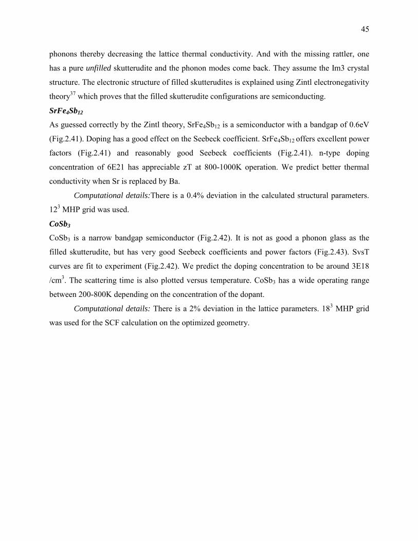
phonons thereby decreasing the lattice thermal conductivity. And with the missing rattler, one
has a pure unfilled skutterudite and the phonon modes come back. They assume the Im3 crystal
structure. The electronic structure of filled skutterudites is explained using Zintl electronegativity
theory37 which proves that the filled skutterudite configurations are semiconducting.
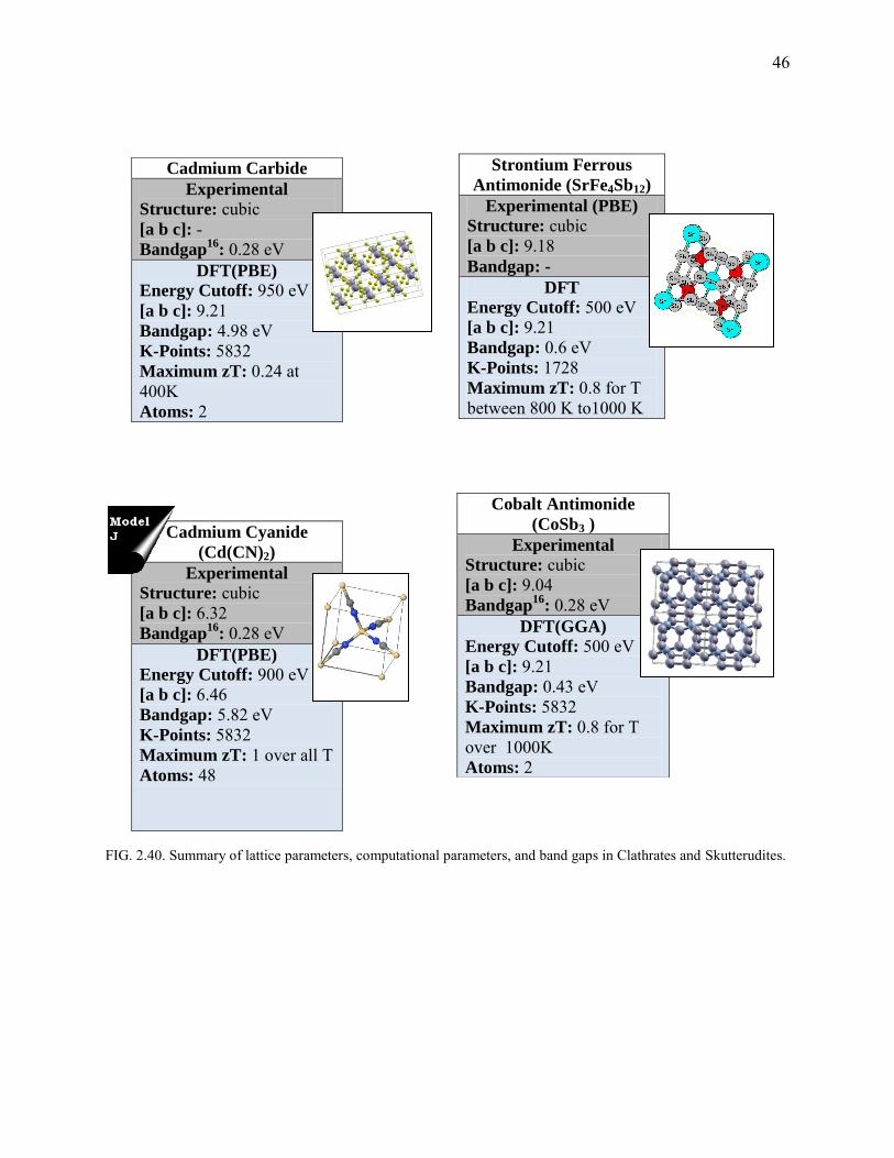
SrFe4Sb12
As guessed correctly by the Zintl theory, SrFe4Sb12 is a semiconductor with a bandgap of 0.6eV
(Fig.2.41). Doping has a good effect on the Seebeck coefficient. SrFe4Sb12 offers excellent power
factors (Fig.2.41) and reasonably good Seebeck coefficients (Fig.2.41). n-type doping
concentration of 6E21 has appreciable zT at 800-1000K operation. We predict better thermal
conductivity when Sr is replaced by Ba.
Computational details:There is a 0.4% deviation in the calculated structural parameters.
123 MHP grid was used.
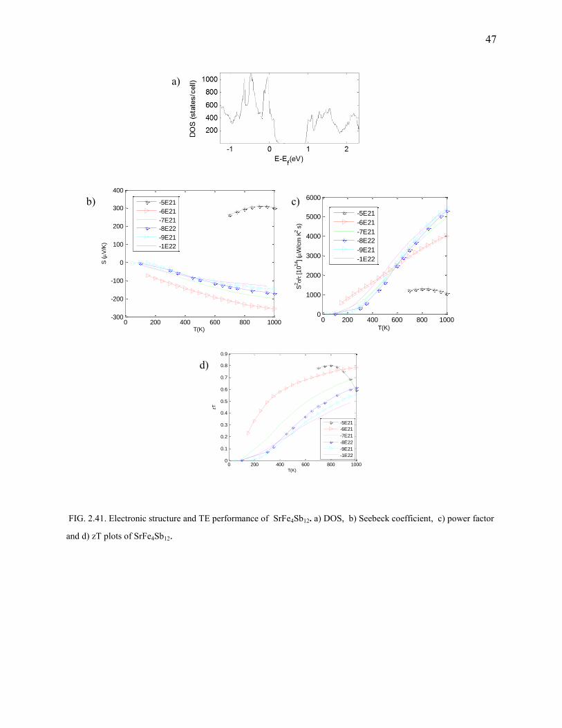
CoSb3
CoSb3 is a narrow bandgap semiconductor (Fig.2.42). It is not as good a phonon glass as the
filled skutterudite, but has very good Seebeck coefficients and power factors (Fig.2.43). SvsT
curves are fit to experiment (Fig.2.42). We predict the doping concentration to be around 3E18
/cm3. The scattering time is also plotted versus temperature. CoSb3 has a wide operating range
between 200-800K depending on the concentration of the dopant.
Computational details: There is a 2% deviation in the lattice parameters. 183 MHP grid
was used for the SCF calculation on the optimized geometry.
46
FIG. 2.40. Summary of lattice parameters, computational parameters, and band gaps in Clathrates and Skutterudites.
Cadmium Carbide
Experimental
Structure: cubic [a b c]: - Bandgap
16: 0.28 eV
DFT(PBE)
Energy Cutoff: 950 eV
[a b c]: 9.21
Bandgap: 4.98 eV
K-Points: 5832
Maximum zT: 0.24 at 400K
Atoms: 2
Strontium Ferrous
Antimonide (SrFe4Sb12)
Experimental (PBE)
Structure: cubic [a b c]: 9.18
Bandgap: -
DFT
Energy Cutoff: 500 eV
[a b c]: 9.21
Bandgap: 0.6 eV
K-Points: 1728
Maximum zT: 0.8 for T between 800 K to1000 K
Cadmium Cyanide
(Cd(CN)2)
Experimental
Structure: cubic [a b c]: 6.32
Bandgap16
: 0.28 eV
DFT(PBE)
Energy Cutoff: 900 eV
[a b c]: 6.46
Bandgap: 5.82 eV
K-Points: 5832
Maximum zT: 1 over all T
Atoms: 48
Cobalt Antimonide
(CoSb3 )
Experimental
Structure: cubic [a b c]: 9.04
Bandgap16
: 0.28 eV
DFT(GGA)
Energy Cutoff: 500 eV
[a b c]: 9.21
Bandgap: 0.43 eV
K-Points: 5832
Maximum zT: 0.8 for T over 1000K
Atoms: 2
47
FIG. 2.41. Electronic structure and TE performance of SrFe4Sb12. a) DOS, b) Seebeck coefficient, c) power factor
and d) zT plots of SrFe4Sb12.
0 200 400 600 800 1000-300
-200
-100
0
100
200
300
400
T(K)
S (V
/K)
-5E21
-6E21
-7E21
-8E22
-9E21
-1E22
0 200 400 600 800 10000
1000
2000
3000
4000
5000
6000
T(K)
S2/
[1
014] (
W/c
m K
2 s
)
-5E21
-6E21
-7E21
-8E22
-9E21
-1E22
0 200 400 600 800 10000
0.1
0.2
0.3
0.4
0.5
0.6
0.7
0.8
0.9
T(K)
zT
-5E21
-6E21
-7E21
-8E22
-9E21
-1E22
b) c)
d)
a)
48
FIG. 2.42. Unfilled CoSb3 electronic structure and S-T experimental fits to compute τ-T and zT. a) DOS, Seebeck
coefficient, power factor and zT plots (b-d) of CoSb3 fit to experiments.
-6 -4 -2 0 2 4 6
50
100
150
200
250 CoSb3
Energy (eV)
DO
S(s
tate
s/c
ell)
150 200 250 300 350 400 450
-300
-250
-200
-150
T(K)
S (V
/K)
log10
Nd(/cm3)=19
Theory
Exp.
150 200 250 300 350 400 45060
70
80
90
100
110
120
130
140
T(K)
(f
s)
log10
Nd(/cm3)=19
150 200 250 300 350 400 4500.68
0.7
0.72
0.74
0.76
0.78
T(K)
zT
a)
b)
d)
c)
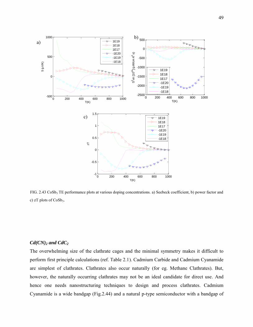
49
FIG. 2.43 CoSb3 TE performance plots at various doping concentrations. a) Seebeck coefficient, b) power factor and
c) zT plots of CoSb3.
Cd(CN)2 and CdC2
The overwhelming size of the clathrate cages and the minimal symmetry makes it difficult to
perform first principle calculations (ref. Table 2.1). Cadmium Carbide and Cadmium Cyanamide
are simplest of clathrates. Clathrates also occur naturally (for eg. Methane Clathrates). But,
however, the naturally occurring clathrates may not be an ideal candidate for direct use. And
hence one needs nanostructuring techniques to design and process clathrates. Cadmium
Cyanamide is a wide bandgap (Fig.2.44) and a natural p-type semiconductor with a bandgap of
0 200 400 600 800 1000-500
0
500
1000
T(K)
S (V
/K)
1E19
1E18
1E17
-1E20
-1E19
-1E18
0 200 400 600 800 1000-2500
-2000
-1500
-1000
-500
0
500
T(K)
S2/
[1
014] (
W/c
m K
2 s
)
1E19
1E18
1E17
-1E20
-1E19
-1E18
0 200 400 600 800 1000-1
-0.5
0
0.5
1
1.5
T(K)
zT
1E19
1E18
1E17
-1E20
-1E19
-1E18
a) b)
c)
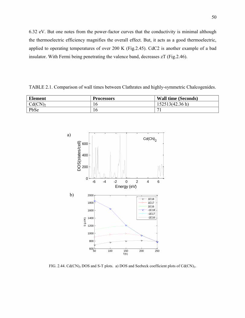
50
6.32 eV. But one notes from the power-factor curves that the conductivity is minimal although
the thermoelectric efficiency magnifies the overall effect. But, it acts as a good thermoelectric,
applied to operating temperatures of over 200 K (Fig.2.45). CdC2 is another example of a bad
insulator. With Fermi being penetrating the valence band, decreases zT (Fig.2.46).
TABLE 2.1. Comparison of wall times between Clathrates and highly-symmetric Chalcogenides.
Element Processors Wall time (Seconds)
Cd(CN)2 16 152513(42.36 h) PbSe 16 71
FIG. 2.44. Cd(CN)2 DOS and S-T plots. a) DOS and Seebeck coefficient plots of Cd(CN)2.
-6 -4 -2 0 2 4 60
200
400
600
Cd(CN)2
Energy (eV)
DO
S(s
tate
s/c
ell)
50 100 150 200 250600
800
1000
1200
1400
1600
1800
2000
T(K)
S (V
/K)
1E18
1E17
1E16
-1E18
-1E17
-1E16
a)
b)

51
FIG. 2.45. Cd(CN)2 pf-T and zT curves at various doping levels. a) power factor and b) zT plots of Cd(CN)2.
50 100 150 200 250-60
-40
-20
0
20
40
60
T(K)
S2/
[1
014] (
W/c
m K
2 s
)
1E18
1E17
1E16
-1E18
-1E17
-1E16
50 100 150 200 250-1
-0.5
0
0.5
1
T(K)
zT
1E18
1E17
1E16
-1E18
-1E17
-1E16
a)
b)
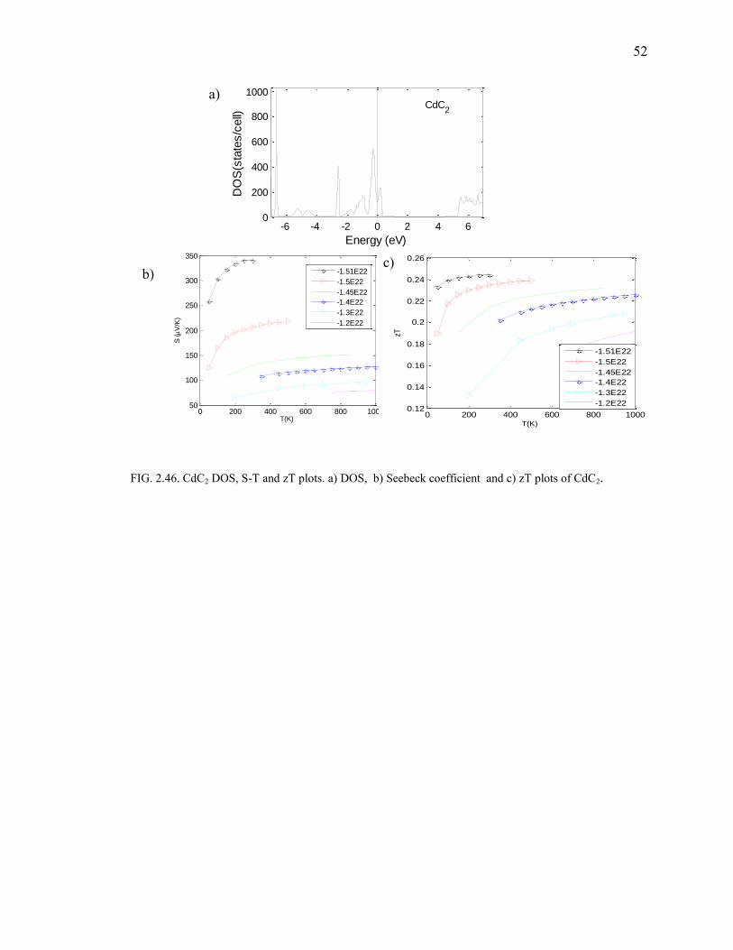
52
FIG. 2.46. CdC2 DOS, S-T and zT plots. a) DOS, b) Seebeck coefficient and c) zT plots of CdC2.
-6 -4 -2 0 2 4 60
200
400
600
800
1000
CdC2
Energy (eV)D
OS
(sta
tes/c
ell)
0 200 400 600 800 100050
100
150
200
250
300
350
T(K)
S (V
/K)
-1.51E22
-1.5E22
-1.45E22
-1.4E22
-1.3E22
-1.2E22
0 200 400 600 800 10000.12
0.14
0.16
0.18
0.2
0.22
0.24
0.26
T(K)
zT
-1.51E22
-1.5E22
-1.45E22
-1.4E22
-1.3E22
-1.2E22
a)
b) c)
53
CHAPTER III
THE SPECIAL CASE OF LaCoO3
Spin state transitions are usually attributed to a pressure variation, or triggered by an external E-
field/magnetic perturbation (like - the behavior of a paramagnetic, often put to use in spin valves
and spin flip techniques38) or are temperature driven. LaCoO3 shows a similar spin state
transition where magnetism shows up at about 100K. A procedure that enables the calculation of
transport coefficients even in the presence of such phase transformations is outlined in this
chapter. The transition temperature of LaCoO3 is found to be 110 K which is 10% off the actual
result39 (~100K).
Two separate states of LaCoO3 were initially prepared: an unadulterated state with lattice
parameters obtained from ICSD, while the other state employs an overridden initial spin state
(S=1). The geometries undergo full cell optimization with the aforementioned constraints with 83
(MHP) k-points in the irreducible wedge. A separate SCF calculation at an increased k (123)
concentration helps retrieve dense ground state energies about the special points in the Brillouin
zone, which are then supplied to BoltzTrap40 as input. As expected, LaCoO3 shows a Mott-
behavior (ref. Fig.3.1, Fig3.2) unless one employs a L(S)DA+U. Similar effective (U-J) values
were used for the High Spin (HS) state due to the absence of XPS data. Such an assumption
could be one of the contributing factors to the ~10% error in the observation. Effective |U-J|
parameters for Co are computed from the binding energies obtained from XPS data. “Density
functional study of CO on Rh(111)” 41
is a formal discussion on the "how-to".
One notes from table 3.1 that the d electron occupancies are not whole numbers. DFT
algorithms use integration techniques (over the charge density) that would obviously return a
fractional component. Depending on the density of the k-mesh, the least significant digit (LSD)
could be truncated. In general, fractional occupancies of less than unity are thanks to the
hybridization of electrons. But anything over a 0.9 could be assumed to have minimal covalent
character. The VASP input format of FERDO and FERWE (for spin polarized cases) requires
that one fill the occupancies corresponding to a particular band by hand. There is, however no
direct procedure to specify "d-states" for a particular atom exclusively. Establishing a relation
between band energies and atom specific states requires a brute-force technique of scanning over
each band to locate a specific d electron. Alternately, one could also use a small smear value (but
a)
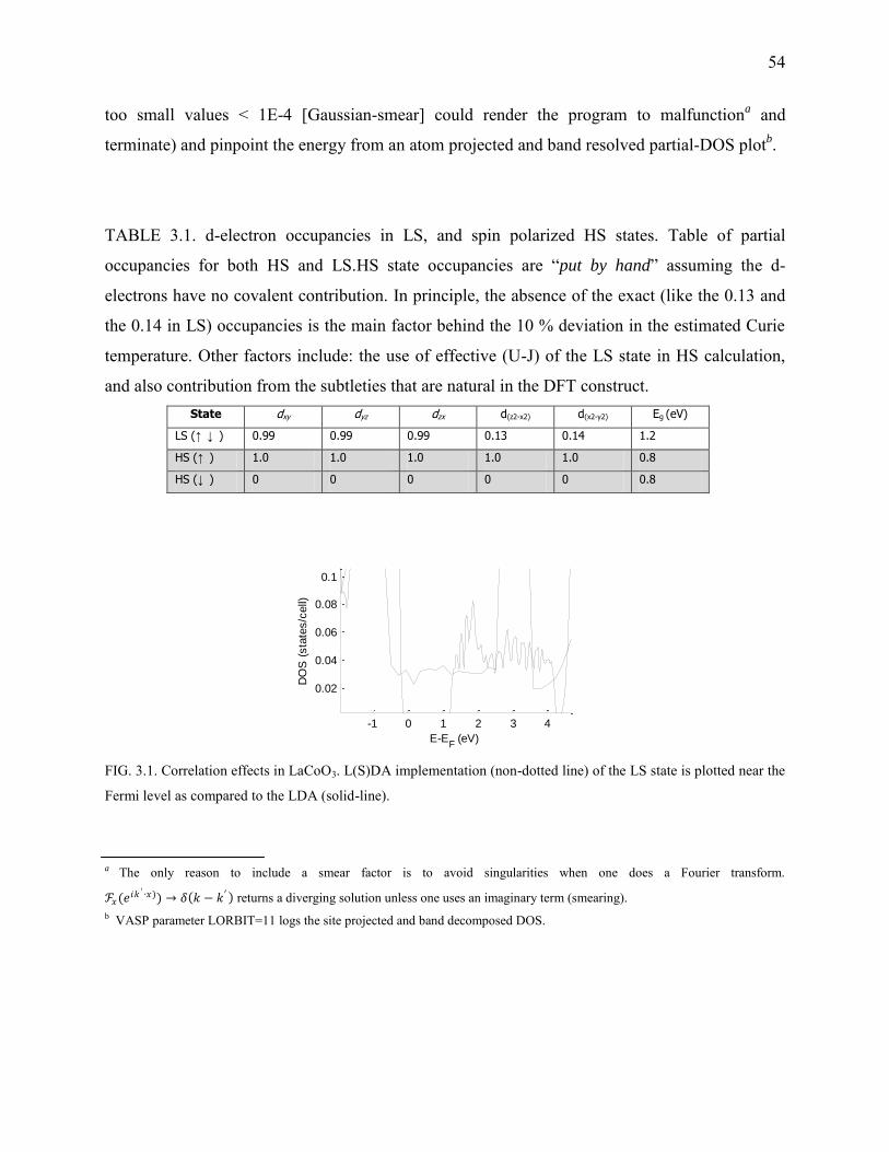
54
too small values < 1E-4 [Gaussian-smear] could render the program to malfunctiona and
terminate) and pinpoint the energy from an atom projected and band resolved partial-DOS plotb.
TABLE 3.1. d-electron occupancies in LS, and spin polarized HS states. Table of partial
occupancies for both HS and LS.HS state occupancies are “put by hand” assuming the d-
electrons have no covalent contribution. In principle, the absence of the exact (like the 0.13 and
the 0.14 in LS) occupancies is the main factor behind the 10 % deviation in the estimated Curie
temperature. Other factors include: the use of effective (U-J) of the LS state in HS calculation,
and also contribution from the subtleties that are natural in the DFT construct. State dxy dyz dzx d(z2-x2) d(x2-y2) Eg (eV)
LS (↑ ↓ ) 0.99 0.99 0.99 0.13 0.14 1.2
HS (↑ ) 1.0 1.0 1.0 1.0 1.0 0.8
HS (↓ ) 0 0 0 0 0 0.8
FIG. 3.1. Correlation effects in LaCoO3. L(S)DA implementation (non-dotted line) of the LS state is plotted near the
Fermi level as compared to the LDA (solid-line).
a The only reason to include a smear factor is to avoid singularities when one does a Fourier transform.
ℱ𝑥(𝑒𝑖𝑘 ′ ∙𝑥)) → 𝛿 𝑘 − 𝑘′ returns a diverging solution unless one uses an imaginary term (smearing). b VASP parameter LORBIT=11 logs the site projected and band decomposed DOS.
-1 0 1 2 3 4
0.02
0.04
0.06
0.08
0.1
E-EF (eV)
DO
S (
sta
tes/c
ell)
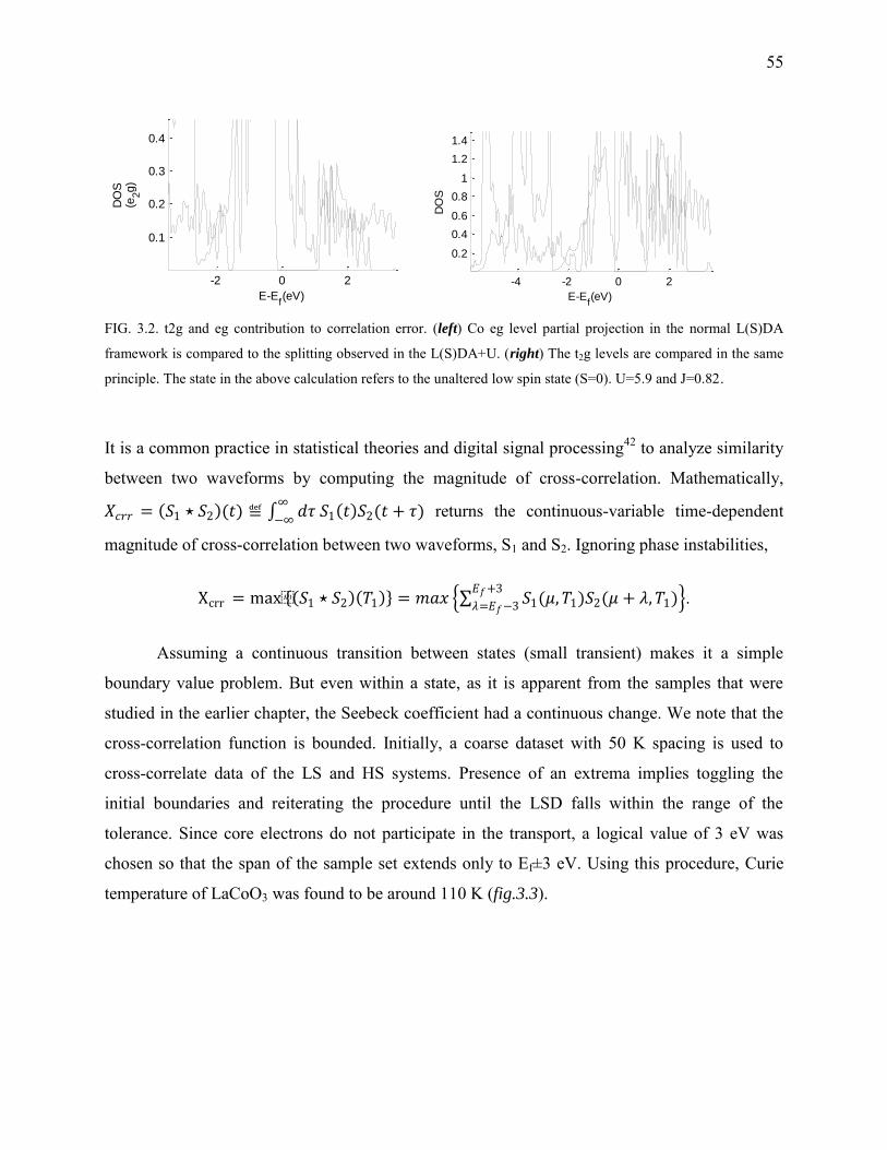
55
FIG. 3.2. t2g and eg contribution to correlation error. (left) Co eg level partial projection in the normal L(S)DA
framework is compared to the splitting observed in the L(S)DA+U. (right) The t2g levels are compared in the same
principle. The state in the above calculation refers to the unaltered low spin state (S=0). U=5.9 and J=0.82.
It is a common practice in statistical theories and digital signal processing42 to analyze similarity
between two waveforms by computing the magnitude of cross-correlation. Mathematically,
𝑋𝑐𝑟𝑟 = 𝑆1 ⋆ 𝑆2 (𝑡) ≝ 𝑑𝜏 𝑆1 𝑡 𝑆2(𝑡 + 𝜏)∞
−∞ returns the continuous-variable time-dependent
magnitude of cross-correlation between two waveforms, S1 and S2. Ignoring phase instabilities,
Xcrr = max 𝑆1 ⋆ 𝑆2 𝑇1 = 𝑚𝑎𝑥 𝑆1(𝜇, 𝑇1)𝑆2(𝜇 + 𝜆, 𝑇1)𝐸𝑓+3
𝜆=𝐸𝑓−3 .
Assuming a continuous transition between states (small transient) makes it a simple
boundary value problem. But even within a state, as it is apparent from the samples that were
studied in the earlier chapter, the Seebeck coefficient had a continuous change. We note that the
cross-correlation function is bounded. Initially, a coarse dataset with 50 K spacing is used to
cross-correlate data of the LS and HS systems. Presence of an extrema implies toggling the
initial boundaries and reiterating the procedure until the LSD falls within the range of the
tolerance. Since core electrons do not participate in the transport, a logical value of 3 eV was
chosen so that the span of the sample set extends only to Ef±3 eV. Using this procedure, Curie
temperature of LaCoO3 was found to be around 110 K (fig.3.3).
-2 0 2
0.1
0.2
0.3
0.4
E-Ef(eV)
DO
S(e
2g)
-4 -2 0 2
0.2
0.4
0.6
0.8
1
1.2
1.4
E-Ef(eV)
DO
S
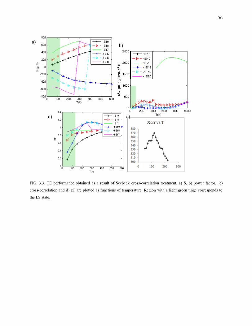
56
FIG. 3.3. TE performance obtained as a result of Seebeck cross-correlation treatment. a) S, b) power factor, c)
cross-correlation and d) zT are plotted as functions of temperature. Region with a light green tinge corresponds to
the LS state.
a) b)
c) d)
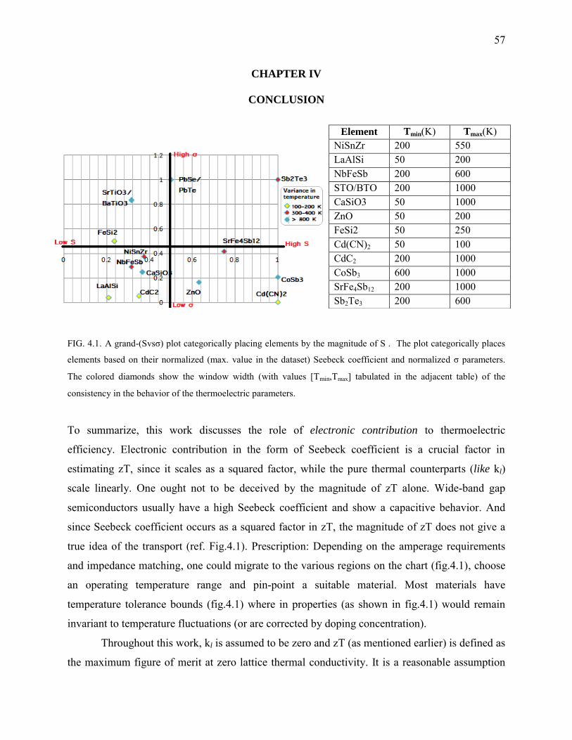
57
CHAPTER IV
CONCLUSION
FIG. 4.1. A grand-(Svsσ) plot categorically placing elements by the magnitude of S . The plot categorically places
elements based on their normalized (max. value in the dataset) Seebeck coefficient and normalized σ parameters.
The colored diamonds show the window width (with values [Tmin,Tmax] tabulated in the adjacent table) of the
consistency in the behavior of the thermoelectric parameters.
To summarize, this work discusses the role of electronic contribution to thermoelectric
efficiency. Electronic contribution in the form of Seebeck coefficient is a crucial factor in
estimating zT, since it scales as a squared factor, while the pure thermal counterparts (like kl)
scale linearly. One ought not to be deceived by the magnitude of zT alone. Wide-band gap
semiconductors usually have a high Seebeck coefficient and show a capacitive behavior. And
since Seebeck coefficient occurs as a squared factor in zT, the magnitude of zT does not give a
true idea of the transport (ref. Fig.4.1). Prescription: Depending on the amperage requirements
and impedance matching, one could migrate to the various regions on the chart (fig.4.1), choose
an operating temperature range and pin-point a suitable material. Most materials have
temperature tolerance bounds (fig.4.1) where in properties (as shown in fig.4.1) would remain
invariant to temperature fluctuations (or are corrected by doping concentration).
Throughout this work, kl is assumed to be zero and zT (as mentioned earlier) is defined as
the maximum figure of merit at zero lattice thermal conductivity. It is a reasonable assumption
Element Tmin(K) Tmax(K) NiSnZr 200 550 LaAlSi 50 200 NbFeSb 200 600 STO/BTO 200 1000 CaSiO3 50 1000 ZnO 50 200 FeSi2 50 250 Cd(CN)2 50 100 CdC2 200 1000 CoSb3 600 1000 SrFe4Sb12 200 1000 Sb2Te3 200 600

58
keeping in view the latest improvements in phonon engineering, Clathrate & filled Skutterudite
systems, and mixed solutions that tend to decrease the lattice thermal conductivity without
meddling much with the electronic structure. Quantitatively, kl is a product of a rigorous
molecular dynamics simulation exercise. Molecular dynamics incorporating statistical-
mechanical procedures, or (Phonon) Boltzmann transport or response function formulations help
determine the lattice thermal conductivity precisely. It all boils down to proper parameterization
of force-fields for each system. Moreover, the correlated dependence of angle-angle, angle-bond
and all possible parametric permutations of the cross-terms that contain most of the vibrational
information, make the task far from being simple and general.
Two band models that were proposed in this work, offer a heuristic perspective to predict
the essential thermoelectric parameters and most of all the models could be effectively expressed
using toy-model basis functions (Chapter I and Chapter II). Advanced models and highly
delocalized states that do not have steep band-edge could also be treated using toy models by
introducing a random and scaled variation in the functional form of E(k) (similar to Anderson’s
localization in disordered systems).
Experimental results have been fit to the calculated values to extract the complicated
relaxation time. The limitations of rigid band approximation (PbSe: where the bandgap is
sensitive to temperature) and constant-phase approximation (Ag2Se: where there is a change of
phase) have been highlighted, and a way to pre-conceive such occurrences are mentioned.
Thermoelectric transport in the presence of a phase-change (like spin-transition) has also been
analyzed and the Curie temperature was determined within a 10% accuracy.
59
REFERENCES
1 C. Kittel, Thermal physics (Wiley, New York,, 1969). 2 G. S. Nolas, D. T. Morelli, and T. M. Tritt, Annual Review of Materials Science 29, 89
(1999). 3 R. G. Parr, Annual Review of Physical Chemistry 34, 631 (1983). 4 E. H. Lieb and B. Simon, Physical Review Letters 31, 681 (1973). 5 D. Jena, A. C. Gossard, and U. K. Mishra, Applied Physics Letters 76, 1707 (2000). 6 A. Szabo and N. S. Ostlund, Modern quantum chemistry: introduction to advanced
electronic structure theory (Dover Publications, Mineola, N.Y., 1996). 7 M. P. Marder, Condensed matter physics (John Wiley, New York, 2000). 8 M. Lundstrom, Fundamentals of carrier transport (Cambridge University Press,
Cambridge, 2000). 9 P. A. M. Dirac, Proceedings of the Royal Society of London Series A-Containing Papers
of a Mathematical and Physical Character 112, 661 (1926). 10 J. Androulakis, C. H. Lin, H. J. Kong, C. Uher, C. Wu, et al., Journal of the American
Chemical Society 129, 9780 (2007). 11 Y. Gelbstein, Z. Dashevsky, and M. P. Dariel, Physica B-Condensed Matter 363, 196
(2005). 12 P. F. P. Poudeu, J. D'Angelo, H. J. Kong, A. Downey, J. L. Short, et al., Journal of the
American Chemical Society 128, 14347 (2006). 13 Y. Zhang, X. Z. Ke, C. F. Chen, J. Yang, and P. R. C. Kent, Physical Review B 80,
024304 (2009). 14 C. M. Fang, R. A. de Groot, and G. A. Wiegers, Journal of Physics and Chemistry of
Solids 63, 457 (2002). 15 N. Piccioli, J. M. Besson, and Balkansk.M, Journal of Physics and Chemistry of Solids
35, 971 (1974). 16 A. Lipovskii, E. Kolobkova, V. Petrikov, I. Kang, A. Olkhovets, et al., Applied Physics
Letters 71, 3406 (1997).

60
17 T. Kyratsi, J. S. Dyck, W. Chen, D. Chung, C. Uher, et al., Journal of Applied Physics
92, 965 (2002). 18 C. M. Bhandari and D. M. Rowe, Thermal conduction in semiconductors (Wiley, New
York, 1988). 19 M. Ferhat and J. Nagao, Journal of Applied Physics 88, 813 (2000). 20 M. Schluter, G. Martinez, and M. L. Cohen, Physical Review B 12, 650 (1975). 21 H. J. Monkhorst and J. D. Pack, Physical Review B 13, 5188 (1976). 22 M. C. S. Kumar and B. Pradeep, Semiconductor Science and Technology 17, 261 (2002). 23 D. Y. Chung, T. Hogan, P. Brazis, M. Rocci-Lane, C. Kannewurf, et al., Science 287,
1024 (2000). 24 G. F. Wang and T. Cagin, Physical Review B 76 (2007). 25 J. Kubler, A. R. Williams, and C. B. Sommers, Physical Review B 28, 1745 (1983). 26 J. Pierre, R. Skolozdra, J. Tobola, S.Kaprzyk, C. Hordequin, et al., Journal of Alloys and
Compounds 262, 101 (1997). 27 H. Hohl, A. P. Ramirez, C. Goldmann, G. Ernst, B. Wölfing, et al., Journal of Physics-
Condensed Matter 11, 1697 (1999). 28 T. Sekimoto, K. Kurosaki, H. Muta, and S. Yamanaka, Journal of Alloys and Compounds
407, 326 (2006). 29 B. R. K. Nanda and I. Dasgupta, Journal of Physics-Condensed Matter 15, 7307 (2003). 30 F. G. Aliev, N. B. Brandt, V. V. Moshchalkov, V. V. Kozyrkov, R. V. Skolozdra, et al.,
Zeitschrift Fur Physik B-Condensed Matter 75, 167 (1989). 31 Q. Shen, L. Chen, T. Goto, T. Hirai, J. Yang, et al., Applied Physics Letters 79, 4165
(2001). 32 N. W. Ashcroft and N. D. Mermin, Solid state physics (Holt, New York,, 1976). 33 S. Ohta, T. Nomura, H. Ohta, and K. Koumoto, Journal of Applied Physics 97 (2005). 34 H. Ohta, Materials Today 10, 44 (2007). 35 V. N. Antonov, O. Jepsen, W. Henrion, M. Rebien, P. Staub, et al., Physical Review B
57, 8934 (1998). 36 N. E. Christensen, Physical Review B 42, 7148 (1990). 37 J. D. Corbett, Chemical Reviews 85, 383 (1985). 38 S. Datta and B. Das, Applied Physics Letters 56, 665 (1990).

61
39 H. Hsu, K. Umemoto, M. Cococcioni, R. Wentzcovitch, Physical Review B 79 (2009). 40 G. K. H. Madsen and D. J. Singh, Computer Physics Communications 175, 67 (2006). 41 L. Kohler and G. Kresse, Physical Review B 70 (2004). 42 J. G. Proakis and D. G. Manolakis, Digital signal processing (Pearson Prentice Hall,
Upper Saddle River, N.J., 2007).
62
VITA
Shiv Akarsh Meka received his Bachelors of Technology in electronics and communication from
VIT, India in 2007. His research interests are centered in quantum transport and strongly
correlated systems. In 2008, he interned at Ames Research Center. He is currently a member of
the IEEE and also a reviewer of Journal of Nanotechnology. He can be reached at:
Shiv Akarsh Meka,
3003 TAMU,
College Station
TX 77843


![In‐situ TEM studies of nanostructured thermoelectric materials: … · cost and high conversion efficiency thermoelectric power generator (TEG).[22–28] Despite those advantages,](https://img.pdfslide.us/doc/110x75/5e37b76cded5da649801e808/inasitu-tem-studies-of-nanostructured-thermoelectric-materials-cost-and-high.jpg)