Embed Size (px)
Citation preview
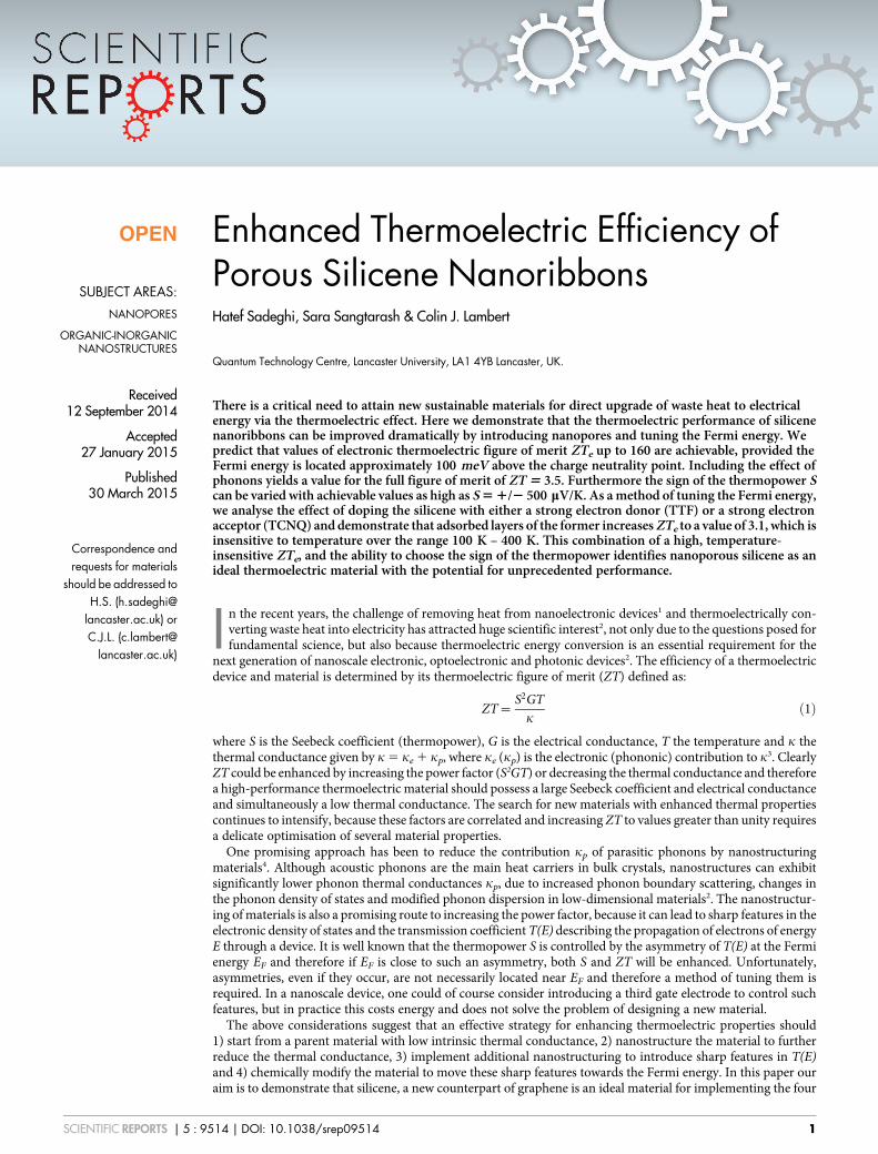
Enhanced Thermoelectric Efficiency ofPorous Silicene NanoribbonsHatef Sadeghi, Sara Sangtarash & Colin J. Lambert
Quantum Technology Centre, Lancaster University, LA1 4YB Lancaster, UK.
There is a critical need to attain new sustainable materials for direct upgrade of waste heat to electricalenergy via the thermoelectric effect. Here we demonstrate that the thermoelectric performance of silicenenanoribbons can be improved dramatically by introducing nanopores and tuning the Fermi energy. Wepredict that values of electronic thermoelectric figure of merit ZTe up to 160 are achievable, provided theFermi energy is located approximately 100 meV above the charge neutrality point. Including the effect ofphonons yields a value for the full figure of merit of ZT 5 3.5. Furthermore the sign of the thermopower Scan be varied with achievable values as high as S 5 1/2 500 mV/K. As a method of tuning the Fermi energy,we analyse the effect of doping the silicene with either a strong electron donor (TTF) or a strong electronacceptor (TCNQ) and demonstrate that adsorbed layers of the former increases ZTe to a value of 3.1, which isinsensitive to temperature over the range 100 K – 400 K. This combination of a high, temperature-insensitive ZTe, and the ability to choose the sign of the thermopower identifies nanoporous silicene as anideal thermoelectric material with the potential for unprecedented performance.
In the recent years, the challenge of removing heat from nanoelectronic devices1 and thermoelectrically con-verting waste heat into electricity has attracted huge scientific interest2, not only due to the questions posed forfundamental science, but also because thermoelectric energy conversion is an essential requirement for the
next generation of nanoscale electronic, optoelectronic and photonic devices2. The efficiency of a thermoelectricdevice and material is determined by its thermoelectric figure of merit (ZT) defined as:
ZT~S2GT
kð1Þ
where S is the Seebeck coefficient (thermopower), G is the electrical conductance, T the temperature and k thethermal conductance given by k 5 ke 1 kp, where ke (kp) is the electronic (phononic) contribution to k3. ClearlyZT could be enhanced by increasing the power factor (S2GT) or decreasing the thermal conductance and thereforea high-performance thermoelectric material should possess a large Seebeck coefficient and electrical conductanceand simultaneously a low thermal conductance. The search for new materials with enhanced thermal propertiescontinues to intensify, because these factors are correlated and increasing ZT to values greater than unity requiresa delicate optimisation of several material properties.
One promising approach has been to reduce the contribution kp of parasitic phonons by nanostructuringmaterials4. Although acoustic phonons are the main heat carriers in bulk crystals, nanostructures can exhibitsignificantly lower phonon thermal conductances kp, due to increased phonon boundary scattering, changes inthe phonon density of states and modified phonon dispersion in low-dimensional materials2. The nanostructur-ing of materials is also a promising route to increasing the power factor, because it can lead to sharp features in theelectronic density of states and the transmission coefficient T(E) describing the propagation of electrons of energyE through a device. It is well known that the thermopower S is controlled by the asymmetry of T(E) at the Fermienergy EF and therefore if EF is close to such an asymmetry, both S and ZT will be enhanced. Unfortunately,asymmetries, even if they occur, are not necessarily located near EF and therefore a method of tuning them isrequired. In a nanoscale device, one could of course consider introducing a third gate electrode to control suchfeatures, but in practice this costs energy and does not solve the problem of designing a new material.
The above considerations suggest that an effective strategy for enhancing thermoelectric properties should1) start from a parent material with low intrinsic thermal conductance, 2) nanostructure the material to furtherreduce the thermal conductance, 3) implement additional nanostructuring to introduce sharp features in T(E)and 4) chemically modify the material to move these sharp features towards the Fermi energy. In this paper ouraim is to demonstrate that silicene, a new counterpart of graphene is an ideal material for implementing the four
OPEN
SUBJECT AREAS:
NANOPORES
ORGANIC-INORGANICNANOSTRUCTURES
Received12 September 2014
Accepted27 January 2015
Published
Correspondence andrequests for materials
should be addressed toH.S. (h.sadeghi@
lancaster.ac.uk) orC.J.L. (c.lambert@
lancaster.ac.uk)
SCIENTIFIC REPORTS | 5 : 9514 | DOI: 10.1038/srep09514 1
30 March 2015
key elements of this strategy, because it is not only CMOS-compat-ible, but also it possesses a low intrinsic thermal conductance, whichcan be further reduced by nanostructuring the material to formnanoribbons.
Since silicon is the most common material used in the electronicsindustry, it is highly desirable to utilise silicon-compatible materialsfor thermoelectric energy conversion. Bulk silicon has a very low ZT(<0.01) and therefore as a first step in a strategy for enhancingthermoelectric performance it is natural to focus on silicene, whichis a recently-observed one-atom-thick crystalline form of siliconatoms arranged in a slightly buckled honeycomb lattice structure5–12.Silicene nanoribbons have been synthesised on silver (111)7,13–25, gold(110)26, iridium (111)27 and the zirconium diboride (0001)28,29 sub-strates and are predicted to be stable on non-metallic substrates30.Calculations of thermoelectric properties of armchair and zigzagsilicene nanoribbons with and without hydrogen-passivated edgessuggest that this material may be attractive for thermoelectricdevices31–34, because the thermal conductivity of 2D silicene is pre-dicted to be much smaller than bulk silicon and its counterpartgraphene35, with only ,10% of the total phononic thermal conduc-tivity being due to the out-of-plane acoustic phonons36,37. Bothof these desirable features arise from the presence of smallbuckling, which breaks the reflection symmetry of the structure35,36.
Further reductions in the phonon contribution arise from addi-tional nanostructuring. For example the thermal conductivity
of a silicene nanosheet sSiNSp ~ 6{30½ �W=mK
� �31,35–37 reduces to
sZSiNRp ~ 0:16{1:4½ �W=mK
� �in zigzag silicene nanoribbons32–34.
This could be potentially even lower in porous silicene, since thelattice thermal conductivity is reduced in nanoporous semi-conductors38 such as nanoporous Bi39, Ge40, graphene41–43, Bi2Te3
44
and SiGe45. Moreover, it is been shown that placing nanopores inbulk silicon greatly reduces the thermal conductivity and enhancesZT by the factor of two46.
Since the low phonon thermal conductance of silicene is wellestablished and therefore elements 1) and 2) of the above strategyare satisfied, in this paper we focus steps 3) and 4) and demonstratethat they can be achieved by inserting nanopores into silicene nanor-ibbons, whose edges are terminated by hydrogen or oxygen and byintroducing adsorbates to tune the position of features in T(E) rela-tive to EF. In view of the low value of kp, we will focus primarily on theelectron contribution in thermoelectric figure of merit ZTe (obtainedby setting kp 5 0 in equation 1) and show that for ribbons containingnanopores with hydrogen-passivated edges, ZTe could be enhancedto values as high as 160 at room temperature by creating sharpfeatures in the T(E) and controlling the Fermi energy or by
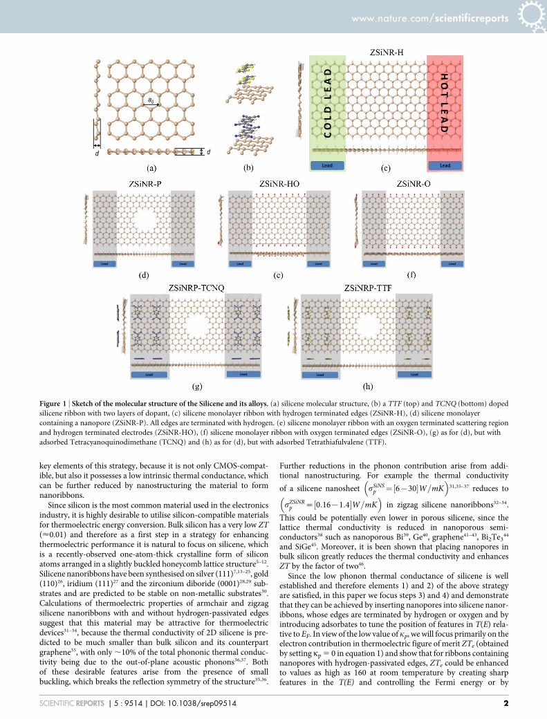
Figure 1 | Sketch of the molecular structure of the Silicene and its alloys. (a) silicene molecular structure, (b) a TTF (top) and TCNQ (bottom) doped
silicene ribbon with two layers of dopant, (c) silicene monolayer ribbon with hydrogen terminated edges (ZSiNR-H), (d) silicene monolayer
containing a nanopore (ZSiNR-P). All edges are terminated with hydrogen. (e) silicene monolayer ribbon with an oxygen terminated scattering region
and hydrogen terminated electrodes (ZSiNR-HO), (f) silicene monolayer ribbon with oxygen terminated edges (ZSiNR-O), (g) as for (d), but with
adsorbed Tetracyanoquinodimethane (TCNQ) and (h) as for (d), but with adsorbed Tetrathiafulvalene (TTF).
www.nature.com/scientificreports
SCIENTIFIC REPORTS | 5 : 9514 | DOI: 10.1038/srep09514 2
introducing adsorbates such as Tetrathiafulvalene (TTF) andTetracyanoquinodimethane (TCNQ) onto the silicene surface. Wewill then show that by including the kp of silicene nanoribbons, ahigh value of the full ZT of order 3.5 is achievable.
Results and DiscussionWe have calculated the electronic contribution to the thermal con-ductance, the Seebeck and Peltier coefficients and ZTe for the struc-
tures shown in Figure 1c–h. The optimized lattice constant (a0) andbuckling (d) of the silicene nanoribbon shown in Figure 1a are foundto be 3.6 A and 0.53 A, respectively, similar to that reported else-where10,32,47. The engineered silicene nanoribbons shown in Figure 1include: a zigzag monolayer silicene nanoribbon with hydrogen ter-minated edges (ZSiNR-H, Figure 1c), a zigzag monolayer silicenenanoribbon containing a nanopore with all edges terminated byhydrogen (ZSiNR-P, Figure 1d), a zigzag monolayer silicene nanor-
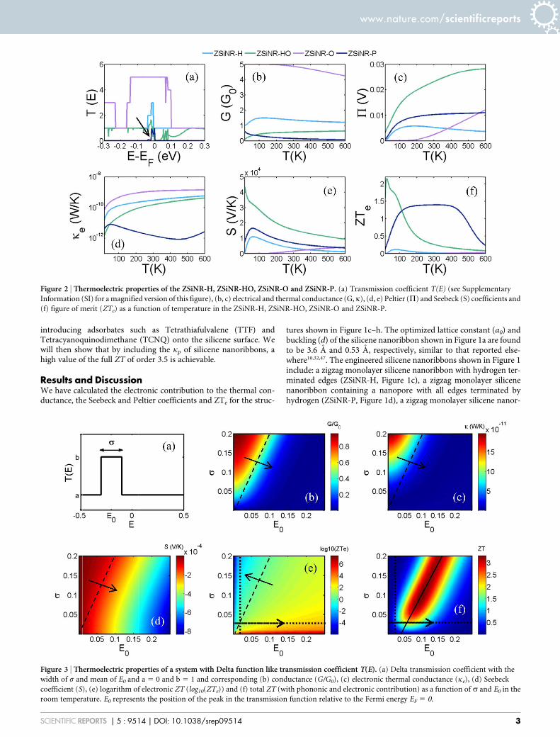
Figure 2 | Thermoelectric properties of the ZSiNR-H, ZSiNR-HO, ZSiNR-O and ZSiNR-P. (a) Transmission coefficient T(E) (see Supplementary
Information (SI) for a magnified version of this figure), (b, c) electrical and thermal conductance (G, k), (d, e) Peltier (P) and Seebeck (S) coefficients and
(f) figure of merit (ZTe) as a function of temperature in the ZSiNR-H, ZSiNR-HO, ZSiNR-O and ZSiNR-P.
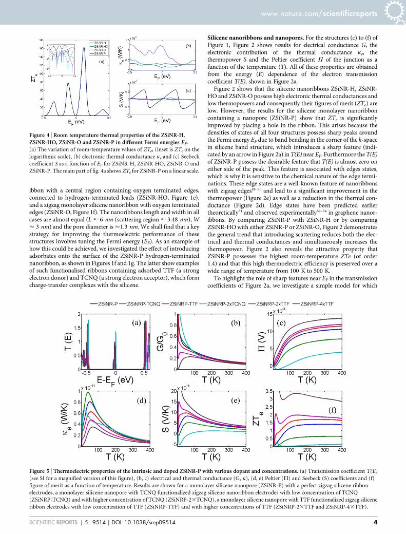
Figure 3 | Thermoelectric properties of a system with Delta function like transmission coefficient T(E). (a) Delta transmission coefficient with the
width of s and mean of E0 and a 5 0 and b 5 1 and corresponding (b) conductance (G/G0), (c) electronic thermal conductance (ke), (d) Seebeck
coefficient (S), (e) logarithm of electronic ZT (log10(ZTe)) and (f) total ZT (with phononic and electronic contribution) as a function of s and E0 in the
room temperature. E0 represents the position of the peak in the transmission function relative to the Fermi energy EF 5 0.
www.nature.com/scientificreports
SCIENTIFIC REPORTS | 5 : 9514 | DOI: 10.1038/srep09514 3
ibbon with a central region containing oxygen terminated edges,connected to hydrogen-terminated leads (ZSiNR-HO, Figure 1e),and a zigzag monolayer silicene nanoribbon with oxygen terminatededges (ZSiNR-O, Figure 1f). The nanoribbons length and width in allcases are almost equal (L < 6 nm (scattering region < 3.48 nm), W< 3 nm) and the pore diameter is <1.3 nm. We shall find that a keystrategy for improving the thermoelectric performance of thesestructures involves tuning the Fermi energy (EF). As an example ofhow this could be achieved, we investigated the effect of introducingadsorbates onto the surface of the ZSiNR-P hydrogen-terminatednanoribbon, as shown in Figures 1f and 1g. The latter show examplesof such functionalised ribbons containing adsorbed TTF (a strongelectron donor) and TCNQ (a strong electron acceptor), which formcharge-transfer complexes with the silicene.
Silicene nanoribbons and nanopores. For the structures (c) to (f) ofFigure 1, Figure 2 shows results for electrical conductance G, theelectronic contribution of the thermal conductance ke, thethermopower S and the Peltier coefficient P of the junction as afunction of the temperature (T). All of these properties are obtainedfrom the energy (E) dependence of the electron transmissioncoefficient T(E), shown in Figure 2a.
Figure 2 shows that the silicene nanoribbons ZSiNR-H, ZSiNR-HO and ZSiNR-O possess high electronic thermal conductances andlow thermopowers and consequently their figures of merit (ZTe) arelow. However, the results for the silicene monolayer nanoribboncontaining a nanopore (ZSiNR-P) show that ZTe is significantlyimproved by placing a hole in the ribbon. This arises because thedensities of states of all four structures possess sharp peaks aroundthe Fermi energy EF due to band bending in the corner of the k-spacein silicene band structure, which introduces a sharp feature (indi-cated by an arrow in Figure 2a) in T(E) near EF. Furthermore the T(E)of ZSiNR-P possess the desirable feature that T(E) is almost zero oneither side of the peak. This feature is associated with edges states,which is why it is sensitive to the chemical nature of the edge termi-nations. These edge states are a well-known feature of nanoribbonswith zigzag edges48–50 and lead to a significant improvement in thethermopower (Figure 2e) as well as a reduction in the thermal con-ductance (Figure 2d). Edge states have been predicted earliertheoretically51 and observed experimentally52–54 in graphene nanor-ibbons. By comparing ZSiNR-P with ZSiNR-H or by comparingZSiNR-HO with either ZSiNR-P or ZSiNR-O, Figure 2 demonstratesthe general trend that introducing scattering reduces both the elec-trical and thermal conductances and simultaneously increases thethermopower. Figure 2 also reveals the attractive property thatZSiNR-P possesses the highest room-temperature ZTe (of order1.4) and that this high thermoelectric efficiency is preserved over awide range of temperature from 100 K to 500 K.
To highlight the role of sharp features near EF in the transmissioncoefficients of Figure 2a, we investigate a simple model for which
Figure 4 | Room temperature thermal properties of the ZSiNR-H,ZSiNR-HO, ZSiNR-O and ZSiNR-P in different Fermi energies EF.(a) The variation of room-temperature values of ZTe, (inset is ZTe on the
logarithmic scale), (b) electronic thermal conductance ke and (c) Seebeck
coefficient S as a function of EF for ZSiNR-H, ZSiNR-HO, ZSiNR-O and
ZSiNR-P. The main part of fig. 4a shows ZTe for ZSiNR-P on a linear scale.
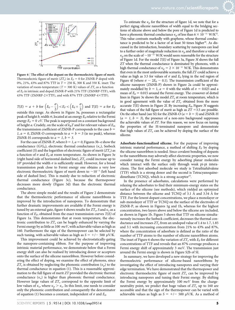
Figure 5 | Thermoelectric properties of the intrinsic and doped ZSiNR-P with various dopant and concentrations. (a) Transmission coefficient T(E)
(see SI for a magnified version of this figure), (b, c) electrical and thermal conductance (G, k), (d, e) Peltier (P) and Seebeck (S) coefficients and (f)
figure of merit as a function of temperature. Results are shown for a monolayer silicene nanopore (ZSiNR-P) with a perfect zigzag silicene ribbon
electrodes, a monolayer silicene nanopore with TCNQ functionalized zigzag silicene nanoribbon electrodes with low concentration of TCNQ
(ZSiNRP-TCNQ) and with higher concentration of TCNQ (ZSiNRP-23TCNQ), a monolayer silicene nanopore with TTF functionalized zigzag silicene
ribbon electrodes with low concentration of TTF (ZSiNRP-TTF) and with higher concentrations of TTF (ZSiNRP-23TTF and ZSiNRP-43TTF).
www.nature.com/scientificreports
SCIENTIFIC REPORTS | 5 : 9514 | DOI: 10.1038/srep09514 4
T(E) 5 a 1 b for E0{s
2
� �vEFv E0z
s
2
� �and T(E) 5 a for EF
outside this range. As shown in Figure 3a, possesses a rectangularpeak of height b, widths, located at an energy E0 relative to the Fermienergy EF 5 0 eV. The peak is superposed on a constant backgroundof height a. Crudely, on the scale of kBT and for relevant values of E0,the transmission coefficient of ZSiNR-P corresponds to the case b 5
1, a 5 0, ZSiNR-O corresponds to a 5 b 5 5 (ie no peak), whereasZSiNR-H corresponds to a 5 1, b 5 3.
For the case of ZSiNR-P, where b 5 1, a 5 0, Figures 3b–e show theconductance (G/G0), electronic thermal conductance (ke), Seebeckcoefficient (S) and the logarithm of electronic figure of merit (ZTe) asa function of s and E0 at room temperature. As shown in Figure 3e(right hand side of horizontal dashed line), ZTe could increase up to106 provided the width s is sufficiently small. However, for a broadtransmission peak close to Fermi energy one obtains a very lowelectronic thermoelectric figure of merit down to ,1025 (left handside of dashed line). This is mainly due to reduction of electronicthermal conductance (Figure 3c), because the thermopowerdecreases more slowly (Figure 3d) than the electronic thermalconductance.
The above simple model and the results of Figure 2 demonstratethat the thermoelectric performance of silicene nanoribbons isimproved by the introduction of nanopores. To demonstrate thatfurther dramatic improvements are available if the Fermi energy istuned by an external gate, figure 4 shows results for ZTe, S and ke as afunction of EF, obtained from the exact transmission curves T(E) ofFigure 1a. This demonstrates that at room temperature, the elec-tronic contribution to ZTe can be hugely enhanced by varying theFermi energy by as little as 100 meV, with achievable values as high as160. Furthermore the sign of the thermopower can be selected bysuch tuning, with achievable values as high as S 5 1/2 500 mV/K.
This improvement could be achieved by electrostatically-gatingthe nanopore-containing ribbon. For the purpose of improvingintrinsic material performance, we demonstrate below that a Fermienergy shift can also be realised by introducing donor or acceptorsonto the surface of the silicene nanoribbon. However before consid-ering the effect of doping, we examine the effect of phonons, sinceZTe is obtained by neglecting the phononic contribution (kp) to thethermal conductance in equation (1). This is a reasonable approxi-mation to the full figure of merit ZT provided the electronic thermalconductance (ke) is higher than phononic thermal conductance.However large values of ZTe correspond to the opposite limit oflow values of ke, where kp . ke. In this limit, one needs to consideronly the phononic contribution and consequently the denominatorof equation (1) becomes a constant, independent of s and E0.
To estimate the kp for the structure of figure 1d, we note that for aperfect zigzag silicene nanoribbon of width equal to the bridging sec-tions of silicene above and below the pore of Figure 1d is predicted tohave a phononic thermal conductance kp of less than 6 3 10211 W/K32.This value contrasts markedly with graphene, whose thermal conduc-tance is predicted to be a factor of at least 50 times higher36. As dis-cussed in the introduction, boundary scattering by nanopores can leadto a further order of magnitude reduction in kp and therefore a value ofkp on the scale of ,10212 W/K would seem reasonable for the structureof Figure 1d. For the model T(E) of Figure 3a, Figure 3f shows the fullZT when the thermal conductance is dominated by phonons, with ahigh thermal conductance of kp 5 2 3 10211 W/K. This demonstratesthat even in the most unfavourable scenario, the full ZT could achieve avalue as high as 3.5 for values of s and E0 lying in the red region ofFigure 4f (where s , 2E0 2 0.1). The transmission coefficient of thesilicene nanopore (ZSiNR-P) shown in Figure 2a could be approxi-mately modelled by b 5 1, a 5 0 with the width of s 5 0.025 and amean of E0 5 0.015 around the Fermi energy. The crossover of dottedlines in Figure 3e shows the model ZTe at room temperature, which isin good agreement with the value of ZTe obtained from the moreaccurate T(E) shown in Figure 2f. By increasing E0, Figure 3f suggeststhat values of the full figure of merit as high as ZT 53.5 are possible.On the other hand (see SI) for the ZSiNR-O (a 5 b 5 5) and ZSiNR-H(a 5 1, b 5 3), the presence of a non-zero background suppressesthe achievable values of ZT. For this reason, we now focus on tuningthe properties of the H-terminated nanopore and demonstratethat high values of ZTe can be achieved by doping the surface of thesilicene.
Adsorbate-functionalized silicene. For the purpose of improvingintrinsic material performance, a method of shifting EF by dopingthe silicene nanoribbon is needed. Since covalent bonding of dopantsto the nanoribbons may adversely affect electronic properties, we nowconsider tuning the Fermi energy by adsorbing planar moleculeswhich interact with the surface only through weak pi-pi intera-ctions. The first adsorbed molecule we study is Tetrathiafulvalene(TTF) which is a strong donor and the second is Tetracyanoquino-dimethane (TCNQ), which is a strong acceptor55.
In the presence of adsorbates, calculations were performed byrelaxing the adsorbates to find their minimum-energy states on thesurface of the silicene (see methods), which yielded an optimizeddistance between the silicene and TCNQ of 3.1 A and 3.54 A forTTF. For the lowest dopant concentrations, we place a monolayer orsub-monolayer of TTF or TCNQ on the surface of the electrodes ofZSiNR-P, as shown in Figures 1g and 1h, whereas for the highestconcentration, two layers above and below the silicene are included,as shown in Figure 1b. Figure 5 shows that TTF on silicene simulta-neously increases the Seebeck coefficient, decreases the thermal con-ductance and increases ZTe from an undoped value of 1.4 to 1.7, 1.85and 3.1 with increasing concentration from 21% to 43% and 87%,where the concentration of adsorbate is defined as the ratio of thenumber of TTF atoms to the number of silicene nanoribbon atoms.The inset of Figure 6 shows the variation of ZTe with EF for differentconcentrations of TTF and reveals that an 87% coverage produces aFermi energy shift of approximately 3 meV. The transmission justaround the Fermi energy is shown in Figure S2b of SI.
In summary, we have developed a new strategy for improving thethermoelectric performance of silicene-based nanoribbons byinvestigating the effect of introducing nanopores and varying theiredge termination. We have demonstrated that the thermopower andelectronic thermoelectric figure of merit ZTe can be improved byintroducing nanopores and tuning their Fermi energy. By shiftingthe Fermi energy by approximately 100 meV from the charge-neutrality point, we predict that huge values of ZTe up to 160 areaccessible and that the sign of the thermopower can be varied withachievable values as high as S 5 1/2 500 mV/K. As a method of
Figure 6 | The effect of the dopant on the thermoelectric figure of merit.Thermoelectric figure of merit (ZTe) in EF 5 0 for ZSiNR-P doped with
0%, 21%, 43% and 87% TTF in T 5 250 K, 300 K and 350 K. inset: The
variation of room-temperature (T 5 300 K) values of ZTe as a function
of EF in intrinsic and doped ZSiNR-P with 21% TTF (ZSiNRP-TTF), with
43% TTF (ZSiNRP-23TTF), and with 87% TTF (ZSiNRP-43TTF).
www.nature.com/scientificreports
SCIENTIFIC REPORTS | 5 : 9514 | DOI: 10.1038/srep09514 5
tuning the Fermi energy, we analysed the effect of doping the silicenewith either a strong electron donor (TTF) or a strong electronacceptor (TCNQ) and demonstrated that doping by the formertended to decrease the value of ZTe, because the Fermi energy shiftwas in an unfavourable direction. On the other hand, we found thatdoping with TTF increased the room-temperature value to ZTe to 3.1and that this value is insensitive to temperature over the range 100 K– 400 K. This combination of a high temperature-insensitive ZTe,and the fact that the low phonon thermal conductance renders ZTe
comparable with the full figure of merit ZT, identifies nanoporoussilicene as an ideal thermoelectric material with the potential forunprecedented performance.
MethodsTo find the optimized geometry and ground state Hamiltonian of the structures ofinterest, we employed the SIESTA56 implementation of Density Functional Theory(DFT) using the generalized gradient approximation (GGA) of the exchange andcorrelation functional with the Perdew-Burke-Ernzerhof parameterization (PBE)57 adouble zeta polarized basis set, a real-space grid defined with a plane wave cut-offenergy of 250 Ry and a maximum force tolerance of 40 meV/Ang. The calculationwith VDW-DF exchange and correlation functional with BH parameterization wasalso carried out to check the GGA-PBE result in some cases. The BH is the same asDRSLL with some modification58. From the converged DFT calculation, the under-lying mean-field Hamiltonian was combined with our transport code, GOLLUM59
which is an implementation of the non-equilibrium Green’s function (NEGF)method. This yields the transmission coefficient T(E) for electrons of energy E(passing from the source to the drain) via the relation
T(E)~Trace fCR(E) GR(E)CL(E) GR{(E)g ð2Þ
In this expression, CL,R(E) 5 i (SL,R(E) 2SL,R{(E)) describes the level broadening due
to the coupling between left (L) and right (R) electrodes and the central scatteringregion, SL,R(E) are the retarded self-energies associated with this coupling and GR 5
(ES 2 H 2SL 2 SR)21 is the retarded Green’s function, where H is the Hamiltonianand S is overlap matrix (both of them obtained from SIESTA). Thermal propertiessuch as the electrical conductance G(T), the electronic contribution of the thermalconductance ke(T), the thermo-power S(T) and the Peltier coefficient P(T) of thejunction as a function of the temperature are given by59:
G(T)~G0L0 ð3Þ
ke(T)~L0L2{L2
1
hTL0ð4Þ
S(T)~{L1
eTL0ð5Þ
P(T)~TS(T) ð6Þ
where
Ln(T)~
ðz?
{?dE E{EFð ÞnT Eð Þ {
Lf Eð ÞLE
� �ð7Þ
and T(E) is the transmission coefficient, f(E) is the Fermi-Dirac probability distri-bution function (f(E) 5 (1 1 exp (E 2 EF/kBT))21), T is the temperature, EF is theFermi energy, G0 5 2e2/h is the conductance quantum, e is electron charge and h is thePlanck’s constant. From these expressions, the electronic contribution to the figure ofmerit ZTe is:
ZTe~L2
1
L0L2{L21
ð8Þ
1. Balandin, A. A. Thermal properties of graphene and nanostructured carbonmaterials. Nat. Mater. 10, 569–581 (2011).
2. Nika, D. L. & Balandin, A. A. Two-dimensional phonon transport in graphene.J. Phys.: Condens. Mat. 24, 233203 (2012).
3. Karamitaheri, H., Neophytou, N., Pourfath, M., Faez, R. & Kosina, H. Engineeringenhanced thermoelectric properties in zigzag graphene nanoribbons. J. Appl.Phys. 111, 054501 (2012).
4. Karamitaheri, H., Pourfath, M., Faez, R. & Kosina, H. Geometrical effects on thethermoelectric properties of ballistic graphene antidot lattices. J. Appl. Phys. 110,054506 (2011).
5. Nakano, H. et al. Soft synthesis of single-crystal silicon monolayer sheets. Angew.Chem. Int. Ed. 45, 6303–6306 (2006).
6. Cahangirov, S., Topsakal, M., Akturk, E., Sahin, H. & Ciraci, S. Two- and One-Dimensional Honeycomb Structures of Silicon and Germanium. Phys. Rev. Lett.102, 236804 (2009).
7. Vogt, P. et al. Silicene: Compelling Experimental Evidence for Graphenelike Two-Dimensional Silicon. Phys. Rev. Lett. 108, 155501 (2012).
8. Kim, J., Fischetti, M. V. & Aboud, S. Structural, electronic, and transportproperties of silicane nanoribbons. Phys. Rev. B. 86, 205323 (2012).
9. Kamal, C., Chakrabarti, A., Banerjee, A. & Deb, S. Silicene Beyond Mono-layers-Different Stacking Configurations And Their Properties. J. Phys.: Condens. Mat.25, 085508 (2013).
10. Sadeghi, H., Bailey, S. & Lambert, C. J. Silicene-based DNA nucleobase sensing.Appl. Phys. Lett. 104, 103104 (2014).
11. Huang, S. T., Kang, W. & Yang, L. Electronic structure and quasiparticle bandgapof silicene structures. Appl. Phys. Lett. 102 (2013).
12. Sadeghi, H. Electrical Transport Model of Silicene as a Channel of Field EffectTransistor. J. Nanosci. Nanotechnol. 14, 4178–4184 (2014).
13. Jamgotchian, H. et al. Growth of silicene layers on Ag (111): unexpected effect ofthe substrate temperature. J. Phys.: Condens. Mat. 24, 172001 (2012).
14. Feng, B. et al. Evidence of Silicene in Honeycomb Structures of Silicon on Ag(111).Nano Lett. 12, 3507–3511 (2012).
15. Enriquez, H., Vizzini, S., Kara, A., Lalmi, B. & Oughaddou, H. Silicene structureson silver surfaces. J. Phys.: Condens. Mat. 24, 314211 (2012).
16. Lalmi, B. et al. Epitaxial growth of a silicene sheet. Appl. Phys. Lett. 97, 223109(2010).
17. Aufray, B. et al. Graphene-like silicon nanoribbons on Ag(110): A possibleformation of silicene. Appl. Phys. Lett. 96, 183102 (2010).
18. Chen, L. et al. Evidence for Dirac Fermions in a Honeycomb Lattice Based onSilicon. Phys. Rev. Lett. 109, 056804 (2012).
19. Padova, P. D. et al. Evidence of Dirac fermions in multilayer silicene. Appl. Phys.Lett. 102, 163106 (2013).
20. Molle, A. et al. Hindering the Oxidation of Silicene with Non-ReactiveEncapsulation. Adv. Funct. Mater. 23, 4340–4344 (2013).
21. Feng, B. et al. Observation of Dirac cone warping and chirality effects in silicene.Acs. Nano. 7, 9049–9054 (2013).
22. Chen, L., Feng, B. & Wu, K. Observation of a possible superconducting gap insilicene on Ag(111) surface. Appl. Phys. Lett. 102, 081602 (2013).
23. Avila, J. et al. Presence of gapped silicene-derived band in the prototypical (3 3 3)silicene phase on silver (111) surfaces. J. Phys.: Condens. Mat. 25, 262001 (2013).
24. Chen, L., Feng, B. & Wu, K. Observation of superconductivity in silicene.arXiv:1301.1431 (2013).
25. Lin, C.-L. et al. Structure of silicene grown on Ag (111). Appl. Phys. Express. 5,045802 (2012).
26. Tchalal, M. R. et al. Formation of one-dimensional self-assembled siliconnanoribbons on Au (110)-(231). Appl. Phys. Lett. 102, 083107 (2013).
27. Meng, L. et al. Buckled Silicene Formation on Ir(111). Nano Lett. 13, 685–690(2013).
28. Fleurence, A. et al. Experimental Evidence for Epitaxial Silicene on Diboride ThinFilms. Phys. Rev. Lett. 108, 245501 (2012).
29. Friedlein, R., Fleurence, A., Sadowski, J. T. & Yamada-Takamura, Y. Tuning ofsilicene-substrate interactions with potassium adsorption. Appl. Phys. Lett. 102,221603 (2013).
30. Kokott, S., Pflugradt, P., Matthes, L. & Bechstedt, F. Nonmetallic substrates forgrowth of silicene: an ab initio prediction. J. Phys.: Condens. Mat. 26, 185002(2014).
31. Zhang, X. et al. Thermal conductivity of silicene calculated using an optimizedStillinger-Weber potential. Phys. Rev. B. 89, 054310 (2014).
32. Pan, L. et al. Thermoelectric properties of armchair and zigzag silicenenanoribbons. Phys. Chem. Chem. Phys. 14, 13588–13593 (2012).
33. Zberecki, K., Wierzbicki, M., Barnas, J. & Swirkowicz, R. Thermoelectric effects insilicene nanoribbons. Phys. Rev. B. 88, 115404 (2013).
34. Yang, K., Cahangirov, S., Cantarero, A., Rubio, A. & D’Agosta, R. Thermoelectricproperties of atomically thin silicene and germanene nanostructures. Phys. Rev. B.89, 125403 (2014).
35. Xie, H., Hu, M. & Bao, H. Thermal conductivity of silicene from first-principles.Appl. Phys. Lett. 104, 131906 (2014).
36. Gu, X. & Yang, R. First-Principles Prediction of Phononic Thermal Conductivityof Silicene: a Comparison with Graphene. arXiv preprint arXiv:1404.2874 (2014).
37. Bo, L. et al. Thermal conductivity of silicene nanosheets and the effect of isotopicdoping. J. Phys. D: Appl. Phys. 47, 165301 (2014).
38. Mingo, N. & Broido, D. A. Thermoelectric power factor of nanoporoussemiconductors. J. Appl. Phys. 101, 014322 (2007).
39. Song, D. W. et al. Thermal conductivity of nanoporous bismuth thin films. Appl.Phys. Lett. 84, 1883–1885 (2004).
40. Lee, J.-H. & Grossman, J. C. Thermoelectric properties of nanoporous Ge. Appl.Phys. Lett. 95, 013106 (2009).
41. Hu, J., Ruan, X. & Chen, Y. P. Thermal Conductivity and Thermal Rectification inGraphene Nanoribbons: A Molecular Dynamics Study. Nano Lett. 9, 2730–2735(2009).
www.nature.com/scientificreports
SCIENTIFIC REPORTS | 5 : 9514 | DOI: 10.1038/srep09514 6
42. Chang, P.-H. & Nikolic, B. K. Edge currents and nanopore arrays in zigzag andchiral graphene nanoribbons as a route toward high-ZT thermoelectrics. Phys.Rev. B. 86 (2012).
43. Mortazavi, B., Potschke, M. & Cuniberti, G. Multiscale modeling of thermalconductivity of polycrystalline graphene sheets. Nanoscale 6, 3344–3352 (2014).
44. Zhang, Y., Xu, G., Han, F., Wang, Z. & Ge, C. Preparation and ThermoelectricProperties of Nanoporous Bi2Te3-Based Alloys. J. Electron. Mater. 39, 1741–1745(2010).
45. Lee, H. et al. Effects of nanoscale porosity on thermoelectric properties of SiGe.J. Appl. Phys. 107, 094308 (2010).
46. Lee, J.-H., Galli, G. A. & Grossman, J. C. Nanoporous Si as an EfficientThermoelectric Material. Nano Lett. 8, 3750–3754 (2008).
47. Ding, Y. & Ni, J. Electronic structures of silicon nanoribbons. Appl. Phys. Lett. 95,083115 (2009).
48. Song, Y. L., Zhang, Y., Zhang, J. M. & Lu, D. B. Effects of the edge shape and thewidth on the structural and electronic properties of silicene nanoribbons. Appl.Surf. Sci. 256, 6313–6317 (2010).
49. Ding, Y. & Wang, Y. Electronic structures of zigzag silicene nanoribbons withasymmetric sp22sp3 edges. Appl. Phys. Lett. 102, 143115 (2013).
50. Ezawa, M. & Nagaosa, N. Interference of Topologically Protected Edge States inSilicene Nanoribbons. Phys. Rev. B 88, 121401(R) (2013).
51. Nakada, K., Fujita, M., Dresselhaus, G. & Dresselhaus, M. S. Edge state in grapheneribbons: Nanometer size effect and edge shape dependence. Phys. Rev. B. 54,17954–17961 (1996).
52. Kobayashi, Y., Fukui, K.-i., Enoki, T., Kusakabe, K. & Kaburagi, Y. Observation ofzigzag and armchair edges of graphite using scanning tunneling microscopy andspectroscopy. Phys. Rev. B. 71, 193406 (2005).
53. Niimi, Y. et al. Scanning tunneling microscopy and spectroscopy of the electroniclocal density of states of graphite surfaces near monoatomic step edges. Phys. Rev.B. 73, 085421 (2006).
54. Lahiri, J., Lin, Y., Bozkurt, P., Oleynik, I. I. & Batzill, M. An extended defect ingraphene as a metallic wire. Nat. Nano. 5, 326–329 (2010).
55. Anderson, P., Lee, P. & Saitoh, M. Remarks on giant conductivity in TTF-TCNQ.Solid State Commun. 13, 595–598 (1973).
56. Soler, J. M. et al. The SIESTA method for ab initio order- N materials simulation.J. Phys.: Condens. Mat. 14, 2745 (2002).
57. Perdew, J. P., Burke, K. & Ernzerhof, M. Generalized Gradient ApproximationMade Simple. Phys. Rev. Lett. 77, 3865–3868 (1996).
58. Berland, K. & Hyldgaard, P. Exchange functional that tests the robustness of theplasmon description of the van der Waals density functional. Phys. Rev. B. 89,035412 (2014).
59. Ferrer, J. et al. GOLLUM: a next-generation simulation tool for electron, thermaland spin transport. New J Phys 16, 093029 (2014).
AcknowledgmentsThis work is supported by UK EPSRC grants EP/K001507/1, EP/J014753/1, EP/H035818/1and the European Union Marie-Curie Network MOLESCO.
Author contributionsH.S. and S.S. have performed the calculations. H.S. and C.J.L. conceived the idea and wrotethe paper.
Additional informationSupplementary information accompanies this paper at http://www.nature.com/scientificreports
Competing financial interests: The authors declare no competing financial interests.
How to cite this article: Sadeghi, H., Sangtarash, S. & Lambert, C.J. EnhancedThermoelectric Efficiency of Porous Silicene Nanoribbons. Sci. Rep. 5, 9514; DOI:10.1038/srep09514 (2015).
This work is licensed under a Creative Commons Attribution 4.0 InternationalLicense. The images or other third party material in this article are included in thearticle’s Creative Commons license, unless indicated otherwise in the credit line; ifthe material is not included under the Creative Commons license, users will needto obtain permission from the license holder in order to reproduce the material. Toview a copy of this license, visit http://creativecommons.org/licenses/by/4.0/
www.nature.com/scientificreports
SCIENTIFIC REPORTS | 5 : 9514 | DOI: 10.1038/srep09514 7

![2D Radial Distribution Function of Silicene - arXiv · 2012-04-13 · (IE) determined the structure of silicene nanoribbons of di erent widths and lenghts [19]. In this paper we report](https://img.pdfslide.us/doc/110x75/5ed0dbab05e5b00b2540fe83/2d-radial-distribution-function-of-silicene-arxiv-2012-04-13-ie-determined.jpg)


![3. Phase analysis · Web viewAs-well as inhibiting thermoelectric properties, porous solids are less mechanically robust than fully dense ones [20], which, combined with shape changes](https://img.pdfslide.us/doc/110x75/5fedb77a127a7e6bee7edcdd/3-phase-analysis-web-view-as-well-as-inhibiting-thermoelectric-properties-porous.jpg)