Embed Size (px)
Citation preview
June 2016 DocID029353 Rev 1 1/24
www.st.com
AN4878 Application note
STEVAL-ISA175V1 three-output isolated flyback converter for smart meter and power line communication systems based on VIPER26HD
Introduction The STEVAL-ISA175V1 evaluation board implements a three output isolated flyback specifically designed to supply the STCOMET smart meter and power line communication system.
The board is developed using the VIPER26HD offline high-voltage converter by STMicroelectronics. The device features an 800 V avalanche-rugged power section, PWM operation at 115 kHz with frequency jittering for lower EMI, current limiting with adjustable set point, on-board soft-start, safe auto-restart after a fault condition and low standby power.
The power supply provides 15 V @ 550 mArms (700 mA peak) to the power line modem (PLM) and the analog circuitry, a post-regulated 5 V @ 100 mA and a 3.3 V @ 200 mA supply through a dedicated DC-DC converter connected on the 15 V rail for digital circuitry and other low voltage parts.
Although the power supply is designed to operate over a wide, 90-264 VAC input voltage range, it can also withstand a maximum AC main up to 440 VAC. The board can even operate with incorrect phase-to-phase connection in a three-phase network, though thermal performance would be worse.
The board can be used in a stand-alone configuration or with the dedicated STCOMET development kit and the PCB layout is specifically designed to fit inside a real meter.
Contents AN4878
2/24 DocID029353 Rev 1
Contents
1 STEVAL-ISA175V1 board overview ................................................ 5
2 Circuit description ......................................................................... 11
2.1 Input stage and filtering ................................................................... 11
2.2 Snubber network ............................................................................. 11
2.3 HV converter ................................................................................... 11
2.4 Output stage.................................................................................... 11
3 Performance data .......................................................................... 13
3.1 Output voltage characteristics ......................................................... 13
3.2 Efficiency and light load measurements .......................................... 14
4 Typical waveforms ........................................................................ 15
5 EMC pre-compliance tests ............................................................ 19
5.1 Conducted noise measurements ..................................................... 19
5.2 Radiated disturbance field strength (EN50065-1 section 7.3) ......... 21
6 Conclusion ..................................................................................... 22
7 Revision history ............................................................................ 23
AN4878 List of tables
DocID029353 Rev 1 3/24
List of tables
Table 1: STEVAL-ISA175V1 board electrical specifications ...................................................................... 5 Table 2: Bill of materials.............................................................................................................................. 8 Table 3: Transformer characteristics ........................................................................................................ 10 Table 4: Load regulation at 115 VAC ......................................................................................................... 13 Table 5: Load regulation at 230 VAC ......................................................................................................... 13 Table 6: Efficiency at typical and maximum load ...................................................................................... 14 Table 7: Load consumption at minimum load (POUT = 0.16 W) ................................................................ 14 Table 8: Required testing for EMC pre-compliance to EN50065 and IEC61000-4 .................................. 19 Table 9: Analyzer setup with quasi-peak detector .................................................................................... 21 Table 10: Document revision history ........................................................................................................ 23
List of figures AN4878
4/24 DocID029353 Rev 1
List of figures
Figure 1: Main PSU schematic ................................................................................................................... 6 Figure 2: Dedicated DC/DC for 3V3 rail schematic .................................................................................... 7 Figure 3: STEVAL-ISA175V1 board (92 x 42mm) ...................................................................................... 7 Figure 4: STEVAL-ISA175V1 board bottom ............................................................................................... 7 Figure 5: Transformer electrical schematic............................................................................................... 10 Figure 6: Transformer bottom view ........................................................................................................... 10 Figure 7: Transformer package schematic ............................................................................................... 10 Figure 8: VOUT1 and IOUT1 under normal operation in TX mode at 115 VAC ............................................... 15 Figure 9: VOUT1 and IOUT1 under normal operation in TX mode at 230 VAC ............................................... 16 Figure 10: VDS and IDS waveforms under normal operation in TX mode at 115 VAC................................. 16 Figure 11: VDS and IDS waveforms under normal operation in TX mode at 230 VAC................................. 17 Figure 12: VOUT1, VDS and IDS waveforms under normal operation at 440 VAC ......................................... 17 Figure 13: Ripple at 115 VAC ..................................................................................................................... 18 Figure 14: Ripple at 230 VAC ..................................................................................................................... 18 Figure 15: Line conducted disturbance..................................................................................................... 20 Figure 16: Neutral conducted disturbance ................................................................................................ 20 Figure 17: Radiated disturbance field strength ......................................................................................... 21
AN4878 STEVAL-ISA175V1 board overview
DocID029353 Rev 1 5/24
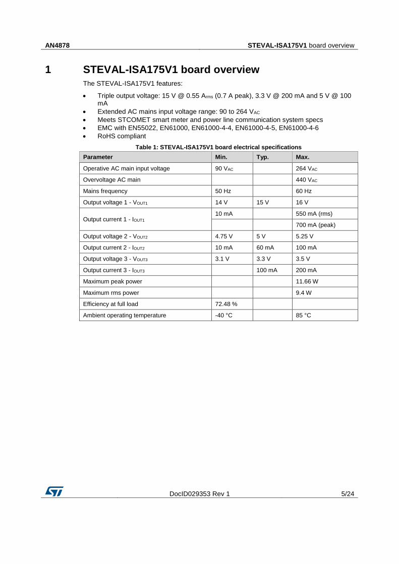
1 STEVAL-ISA175V1 board overview
The STEVAL-ISA175V1 features:
Triple output voltage: 15 V @ 0.55 Arms (0.7 A peak), 3.3 V @ 200 mA and 5 V @ 100 mA
Extended AC mains input voltage range: 90 to 264 VAC
Meets STCOMET smart meter and power line communication system specs
EMC with EN55022, EN61000, EN61000-4-4, EN61000-4-5, EN61000-4-6
RoHS compliant
Table 1: STEVAL-ISA175V1 board electrical specifications
Parameter Min. Typ. Max.
Operative AC main input voltage 90 VAC
264 VAC
Overvoltage AC main
440 VAC
Mains frequency 50 Hz
60 Hz
Output voltage 1 - VOUT1 14 V 15 V 16 V
Output current 1 - IOUT1 10 mA
550 mA (rms)
700 mA (peak)
Output voltage 2 - VOUT2 4.75 V 5 V 5.25 V
Output current 2 - IOUT2 10 mA 60 mA 100 mA
Output voltage 3 - VOUT3 3.1 V 3.3 V 3.5 V
Output current 3 - IOUT3
100 mA 200 mA
Maximum peak power
11.66 W
Maximum rms power
9.4 W
Efficiency at full load 72.48 %
Ambient operating temperature -40 °C
85 °C
STEVAL-ISA175V1 board overview AN4878
6/24 DocID029353 Rev 1
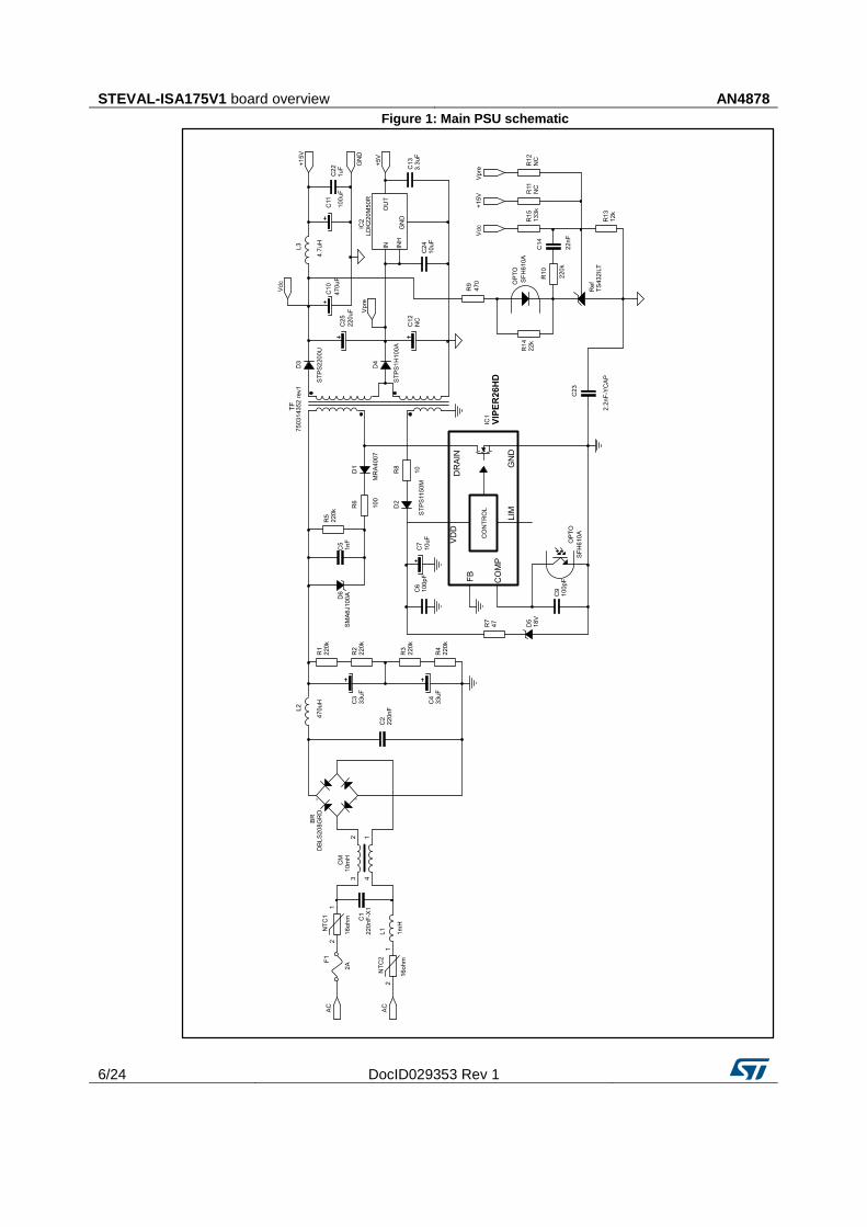
Figure 1: Main PSU schematic
AN4878 STEVAL-ISA175V1 board overview
DocID029353 Rev 1 7/24
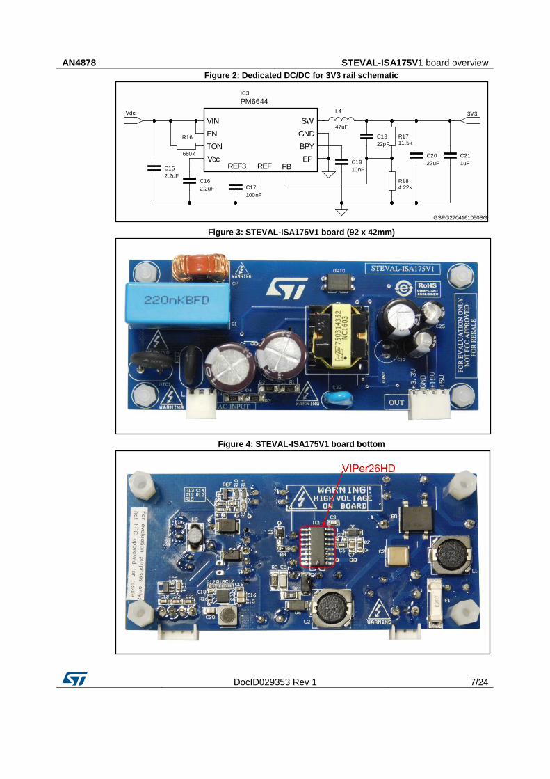
Figure 2: Dedicated DC/DC for 3V3 rail schematic
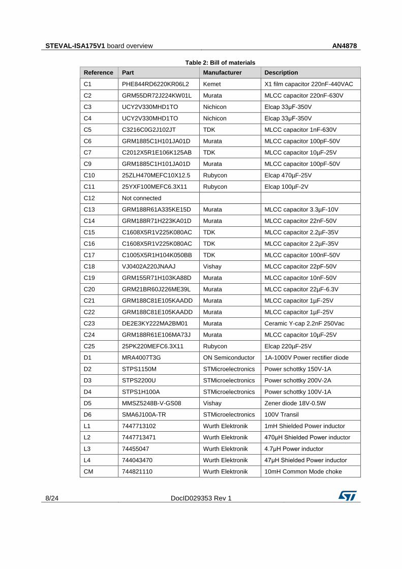
Figure 3: STEVAL-ISA175V1 board (92 x 42mm)
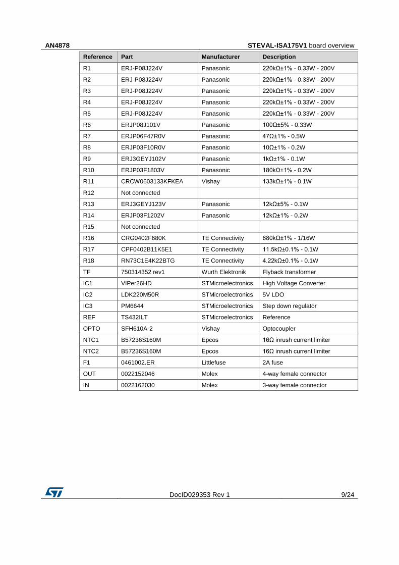
Figure 4: STEVAL-ISA175V1 board bottom
GSPG2704161050SG
Vdc 3V3
R16
680k
C16
2.2uF
R184.22k
C21
1uF
47uF
L4
C15
2.2uF
VIN
Vcc
SW
EPFB
GND
BPY
REFREF3
TON
EN
IC3
PM6644
C18
22pF
C17
100nF
C20
22uF
R1711.5k
C19
10nF
STEVAL-ISA175V1 board overview AN4878
8/24 DocID029353 Rev 1
Table 2: Bill of materials
Reference Part Manufacturer Description
C1 PHE844RD6220KR06L2 Kemet X1 film capacitor 220nF-440VAC
C2 GRM55DR72J224KW01L Murata MLCC capacitor 220nF-630V
C3 UCY2V330MHD1TO Nichicon Elcap 33μF-350V
C4 UCY2V330MHD1TO Nichicon Elcap 33μF-350V
C5 C3216C0G2J102JT TDK MLCC capacitor 1nF-630V
C6 GRM1885C1H101JA01D Murata MLCC capacitor 100pF-50V
C7 C2012X5R1E106K125AB TDK MLCC capacitor 10µF-25V
C9 GRM1885C1H101JA01D Murata MLCC capacitor 100pF-50V
C10 25ZLH470MEFC10X12.5 Rubycon Elcap 470µF-25V
C11 25YXF100MEFC6.3X11 Rubycon Elcap 100µF-2V
C12 Not connected
C13 GRM188R61A335KE15D Murata MLCC capacitor 3.3µF-10V
C14 GRM188R71H223KA01D Murata MLCC capacitor 22nF-50V
C15 C1608X5R1V225K080AC TDK MLCC capacitor 2.2µF-35V
C16 C1608X5R1V225K080AC TDK MLCC capacitor 2.2µF-35V
C17 C1005X5R1H104K050BB TDK MLCC capacitor 100nF-50V
C18 VJ0402A220JNAAJ Vishay MLCC capacitor 22pF-50V
C19 GRM155R71H103KA88D Murata MLCC capacitor 10nF-50V
C20 GRM21BR60J226ME39L Murata MLCC capacitor 22µF-6.3V
C21 GRM188C81E105KAADD Murata MLCC capacitor 1µF-25V
C22 GRM188C81E105KAADD Murata MLCC capacitor 1µF-25V
C23 DE2E3KY222MA2BM01 Murata Ceramic Y-cap 2.2nF 250Vac
C24 GRM188R61E106MA73J Murata MLCC capacitor 10µF-25V
C25 25PK220MEFC6.3X11 Rubycon Elcap 220µF-25V
D1 MRA4007T3G ON Semiconductor 1A-1000V Power rectifier diode
D2 STPS1150M STMicroelectronics Power schottky 150V-1A
D3 STPS2200U STMicroelectronics Power schottky 200V-2A
D4 STPS1H100A STMicroelectronics Power schottky 100V-1A
D5 MMSZ5248B-V-GS08 Vishay Zener diode 18V-0.5W
D6 SMA6J100A-TR STMicroelectronics 100V Transil
L1 7447713102 Wurth Elektronik 1mH Shielded Power inductor
L2 7447713471 Wurth Elektronik 470μH Shielded Power inductor
L3 74455047 Wurth Elektronik 4.7μH Power inductor
L4 744043470 Wurth Elektronik 47μH Shielded Power inductor
CM 744821110 Wurth Elektronik 10mH Common Mode choke
AN4878 STEVAL-ISA175V1 board overview
DocID029353 Rev 1 9/24
Reference Part Manufacturer Description
R1 ERJ-P08J224V Panasonic 220kΩ±1% - 0.33W - 200V
R2 ERJ-P08J224V Panasonic 220kΩ±1% - 0.33W - 200V
R3 ERJ-P08J224V Panasonic 220kΩ±1% - 0.33W - 200V
R4 ERJ-P08J224V Panasonic 220kΩ±1% - 0.33W - 200V
R5 ERJ-P08J224V Panasonic 220kΩ±1% - 0.33W - 200V
R6 ERJP08J101V Panasonic 100Ω±5% - 0.33W
R7 ERJP06F47R0V Panasonic 47Ω±1% - 0.5W
R8 ERJP03F10R0V Panasonic 10Ω±1% - 0.2W
R9 ERJ3GEYJ102V Panasonic 1kΩ±1% - 0.1W
R10 ERJP03F1803V Panasonic 180kΩ±1% - 0.2W
R11 CRCW0603133KFKEA Vishay 133kΩ±1% - 0.1W
R12 Not connected
R13 ERJ3GEYJ123V Panasonic 12kΩ±5% - 0.1W
R14 ERJP03F1202V Panasonic 12kΩ±1% - 0.2W
R15 Not connected
R16 CRG0402F680K TE Connectivity 680kΩ±1% - 1/16W
R17 CPF0402B11K5E1 TE Connectivity 11.5kΩ±0.1% - 0.1W
R18 RN73C1E4K22BTG TE Connectivity 4.22kΩ±0.1% - 0.1W
TF 750314352 rev1 Wurth Elektronik Flyback transformer
IC1 VIPer26HD STMicroelectronics High Voltage Converter
IC2 LDK220M50R STMicroelectronics 5V LDO
IC3 PM6644 STMicroelectronics Step down regulator
REF TS432ILT STMicroelectronics Reference
OPTO SFH610A-2 Vishay Optocoupler
NTC1 B57236S160M Epcos 16Ω inrush current limiter
NTC2 B57236S160M Epcos 16Ω inrush current limiter
F1 0461002.ER Littlefuse 2A fuse
OUT 0022152046 Molex 4-way female connector
IN 0022162030 Molex 3-way female connector
STEVAL-ISA175V1 board overview AN4878
10/24 DocID029353 Rev 1
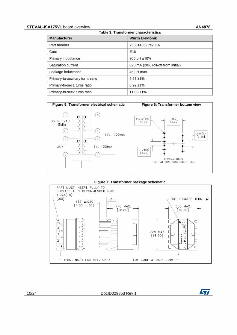
Table 3: Transformer characteristics
Manufacturer Wurth Elektonik
Part number 750314352 rev .6A
Core E16
Primary inductance 900 μH ±10%
Saturation current 820 mA (20% roll-off from initial)
Leakage inductance 45 µH max.
Primary-to-auxiliary turns ratio 5.63 ±1%
Primary-to-sec1 turns ratio 8.92 ±1%
Primary-to-sec2 turns ratio 11.88 ±1%
Figure 5: Transformer electrical schematic
Figure 6: Transformer bottom view
Figure 7: Transformer package schematic
AN4878 Circuit description
DocID029353 Rev 1 11/24
2 Circuit description
2.1 Input stage and filtering
The input stage is appropriately designed to sustain operation up to 440 VAC.
Fuse F1 prevents catastrophic failure and two input NTCs limit the inrush current of the capacitors at plug-in and protect the bridge rectifier (BR); the total required resistance of the NTC is halved to ensure safe operation of the NTC components without exceeding the allowed voltage rate across it.
The total bulk capacitance is achieved by two capacitors in series for a total voltage rate above the maximum operative rectified input voltage (approx. 620 VDC); resistors R1 to R4 ensure equal voltage sharing between the capacitors.
Special emphasis has been placed on filtering the conducted noise of the converter to render power line communication less sensitive to the switching power supply. Both differential and common mode filtering is implemented.
2.2 Snubber network
The R5-C5-D1 clamping network limits the leakage inductance voltage spike by dissipating the related energy at MOSFET turn-off for reliable power supply operation.
Resistor R2 helps further reduce the ringing of the transformer, damping the resonance oscillations at turn-off between leakage inductance and equivalent drain capacitance.
A Transil (D6) is also used to limit the drain voltage in case of voltage exceeding the limits.
2.3 HV converter
The core of the power supply is the VIPER26HD offline high-voltage converter with 800 V avalanche-rugged power section featuring maximum RDS(on) ≤ 7 Ω, and a current-mode 115 kHz fixed frequency PWM controller. The device includes several other features which considerably reduce BOM cost and improve system reliability.
Regulation is achieved by adjusting the voltage on the COMP pin, which transfers output voltage information via the optocoupler. The capacitors and the pin are used for proper loop compensation.
During normal operation, the VDD pin is powered by the auxiliary winding of the transformer. The output of the auxiliary winding is rectified by diode D2 and capacitor C7. Resistor R8 filters auxiliary spikes at turn-off and limits voltage fluctuation on the pin. Capacitor C6 filters any narrow voltage spikes entering the VDD pin. The R7 and D5 clamp network is connected across the VDD pin to avoid transient voltages exceeding the pin absolute maximum rating.
The LIM pin, which is used to adjust the cycle-by-cycle current limitation, is left floating because maximum current limitation is required.
2.4 Output stage
The secondary of the transformer is designed for a two-output option: the secondary windings are wound using a stack arrangement, in order to improve the cross regulation of the non- regulated output.
The first secondary signal is rectified by diode D3 and filtered by output capacitor C10, which is designed to ensure sufficient AC ripple capability to avoid overheating. The L3-
Circuit description AN4878
12/24 DocID029353 Rev 1
C11 post filter further reduces residual output ripple, while capacitor C22 further reduces output switching noise.
The other secondary signal is rectified by diode D4 and capacitor C24; as this output is not directly connected to the feedback loop, an LDO is used to provide a stable and precise +5V output.
Capacitor C25 is added between the cathodes of the diodes to further limit cross regulation between the regulated and unregulated outputs.
The output voltage is sensed by the voltage divider R15 and R13 and compared with the internal 1.24 V reference of the shunt voltage reference TS432; its output is converted, via the optocoupler, into a current signal control for the primary PWM IC.
The 3.3 V output is achieved with a step-down regulator based on the STMicroelectronics PM6644, which allows the construction of a low cost synchronous buck converter based on COT (constant on-time) architecture.
AN4878 Performance data
DocID029353 Rev 1 13/24
3 Performance data
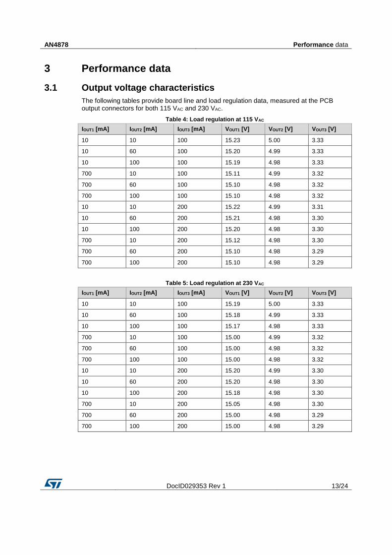
3.1 Output voltage characteristics
The following tables provide board line and load regulation data, measured at the PCB output connectors for both 115 VAC and 230 VAC.
Table 4: Load regulation at 115 VAC
IOUT1 [mA] IOUT2 [mA] IOUT3 [mA] VOUT1 [V] VOUT2 [V] VOUT3 [V]
10 10 100 15.23 5.00 3.33
10 60 100 15.20 4.99 3.33
10 100 100 15.19 4.98 3.33
700 10 100 15.11 4.99 3.32
700 60 100 15.10 4.98 3.32
700 100 100 15.10 4.98 3.32
10 10 200 15.22 4.99 3.31
10 60 200 15.21 4.98 3.30
10 100 200 15.20 4.98 3.30
700 10 200 15.12 4.98 3.30
700 60 200 15.10 4.98 3.29
700 100 200 15.10 4.98 3.29
Table 5: Load regulation at 230 VAC
IOUT1 [mA] IOUT2 [mA] IOUT3 [mA] VOUT1 [V] VOUT2 [V] VOUT3 [V]
10 10 100 15.19 5.00 3.33
10 60 100 15.18 4.99 3.33
10 100 100 15.17 4.98 3.33
700 10 100 15.00 4.99 3.32
700 60 100 15.00 4.98 3.32
700 100 100 15.00 4.98 3.32
10 10 200 15.20 4.99 3.30
10 60 200 15.20 4.98 3.30
10 100 200 15.18 4.98 3.30
700 10 200 15.05 4.98 3.30
700 60 200 15.00 4.98 3.29
700 100 200 15.00 4.98 3.29
Performance data AN4878
14/24 DocID029353 Rev 1
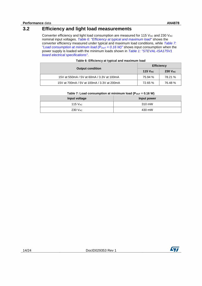
3.2 Efficiency and light load measurements
Converter efficiency and light load consumption are measured for 115 VAC and 230 VAC nominal input voltages. Table 6: "Efficiency at typical and maximum load" shows the converter efficiency measured under typical and maximum load conditions, while Table 7: "Load consumption at minimum load (POUT = 0.16 W)" shows input consumption when the power supply is loaded with the minimum loads shown in Table 1: "STEVAL-ISA175V1 board electrical specifications".
Table 6: Efficiency at typical and maximum load
Output condition Efficiency
115 VAC 230 VAC
15V at 550mA / 5V at 60mA / 3.3V at 100mA 75.94 % 78.21 %
15V at 700mA / 5V at 100mA / 3.3V at 200mA 72.65 % 76.48 %
Table 7: Load consumption at minimum load (POUT = 0.16 W)
Input voltage Input power
115 VAC 310 mW
230 VAC 430 mW
AN4878 Typical waveforms
DocID029353 Rev 1 15/24
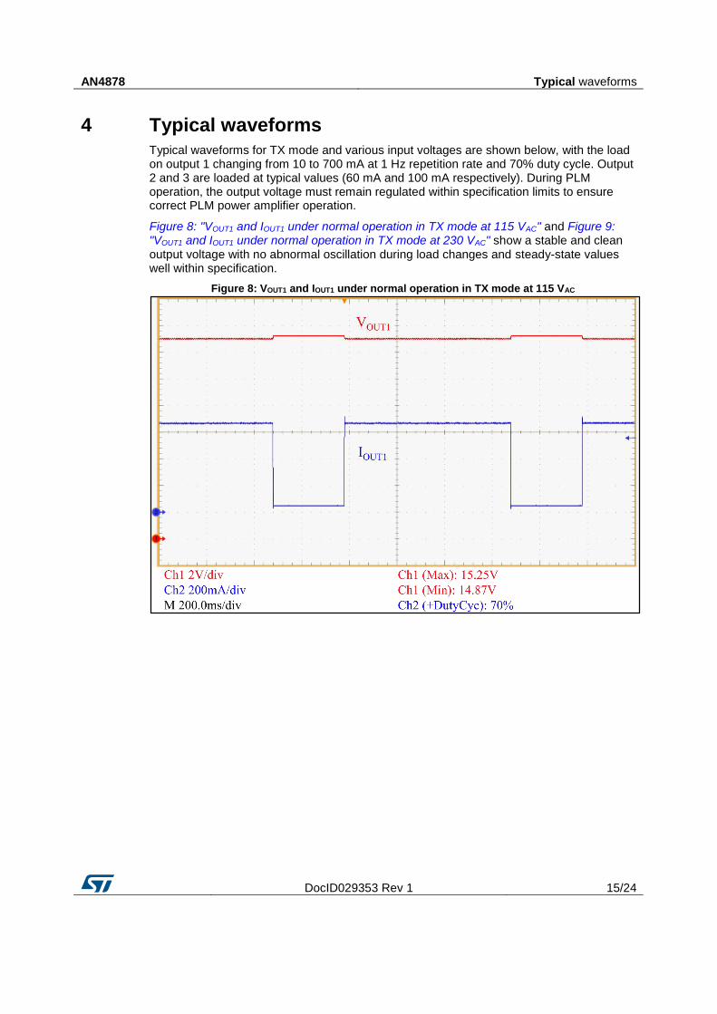
4 Typical waveforms
Typical waveforms for TX mode and various input voltages are shown below, with the load on output 1 changing from 10 to 700 mA at 1 Hz repetition rate and 70% duty cycle. Output 2 and 3 are loaded at typical values (60 mA and 100 mA respectively). During PLM operation, the output voltage must remain regulated within specification limits to ensure correct PLM power amplifier operation.
Figure 8: "VOUT1 and IOUT1 under normal operation in TX mode at 115 VAC" and Figure 9: "VOUT1 and IOUT1 under normal operation in TX mode at 230 VAC" show a stable and clean output voltage with no abnormal oscillation during load changes and steady-state values well within specification.
Figure 8: VOUT1 and IOUT1 under normal operation in TX mode at 115 VAC
Typical waveforms AN4878
16/24 DocID029353 Rev 1
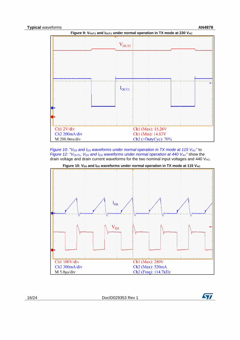
Figure 9: VOUT1 and IOUT1 under normal operation in TX mode at 230 VAC
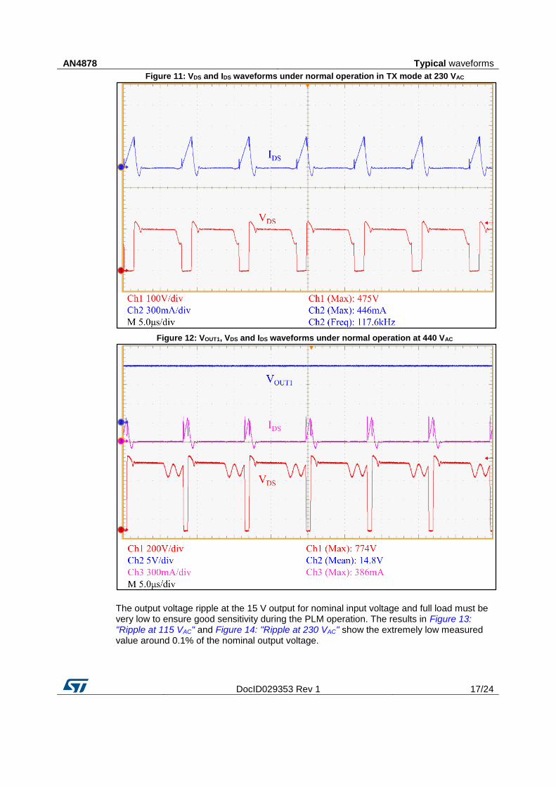
Figure 10: "VDS and IDS waveforms under normal operation in TX mode at 115 VAC" to Figure 12: "VOUT1, VDS and IDS waveforms under normal operation at 440 VAC" show the drain voltage and drain current waveforms for the two nominal input voltages and 440 VAC.
Figure 10: VDS and IDS waveforms under normal operation in TX mode at 115 VAC
AN4878 Typical waveforms
DocID029353 Rev 1 17/24
Figure 11: VDS and IDS waveforms under normal operation in TX mode at 230 VAC
Figure 12: VOUT1, VDS and IDS waveforms under normal operation at 440 VAC
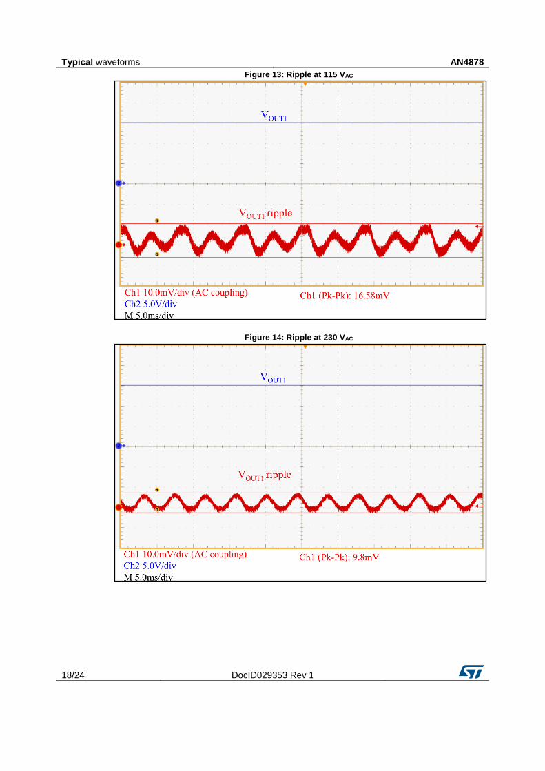
The output voltage ripple at the 15 V output for nominal input voltage and full load must be very low to ensure good sensitivity during the PLM operation. The results in Figure 13: "Ripple at 115 VAC" and Figure 14: "Ripple at 230 VAC" show the extremely low measured value around 0.1% of the nominal output voltage.
Typical waveforms AN4878
18/24 DocID029353 Rev 1
Figure 13: Ripple at 115 VAC
Figure 14: Ripple at 230 VAC
AN4878 EMC pre-compliance tests
DocID029353 Rev 1 19/24
5 EMC pre-compliance tests
EMC pre-compliance tests are required by European standard EN50065 for smart metering PLC applications on low voltage networks (which have the highest EMC test levels) and by IEC61000-4 for Electromagnetic compatibility.
All necessary testing was performed, with positive outcomes, as shown below.
Table 8: Required testing for EMC pre-compliance to EN50065 and IEC61000-4
Type Basic standard
Test Result
Conducted disturbance measurements
EN 55022 Conducted emissions (150 kHz - 30 MHz) Pass
Radiated disturbance measurements
EN 55022 Radiated emissions (30 MHz - 1 GHz Pass
Radiated immunity
EN 61000-4-3 RF radiated fields immunity test (80 - 1000 MHz, 10 V/m)
Pass
EN 61000-4-8 Magnetic 50 Hz field immunity test (100 A/m, 300 A/m)
Pass
Contact/radiated immunity EN 61000-4-2 Electrostatic discharges immunity test (8 kV contact and air mode)
Pass
Conducted immunity
EN 61000-4-4 Fast transients immunity test (2 kV, 5 kHz) Pass
EN 61000-4-5 Surge immunity test (4 kV, common mode and differential mode)
Pass
EN 61000-4-11 Power voltage dips and interruption (30% - 10 ms; 60% - 100 ms; 100% - 5 s)
Pass
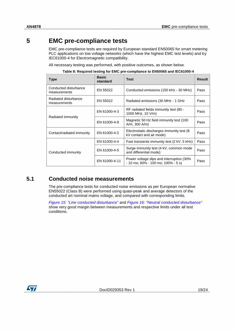
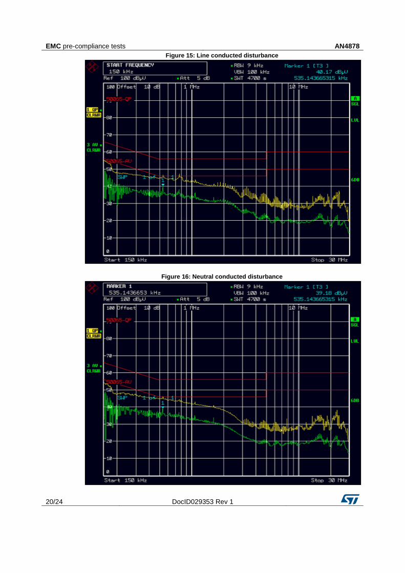
5.1 Conducted noise measurements
The pre-compliance tests for conducted noise emissions as per European normative EN55022 (Class B) were performed using quasi-peak and average detectors of the conducted art nominal mains voltage, and compared with corresponding limits.
Figure 15: "Line conducted disturbance" and Figure 16: "Neutral conducted disturbance" show very good margin between measurements and respective limits under all test conditions.
EMC pre-compliance tests AN4878
20/24 DocID029353 Rev 1
Figure 15: Line conducted disturbance
Figure 16: Neutral conducted disturbance
AN4878 EMC pre-compliance tests
DocID029353 Rev 1 21/24
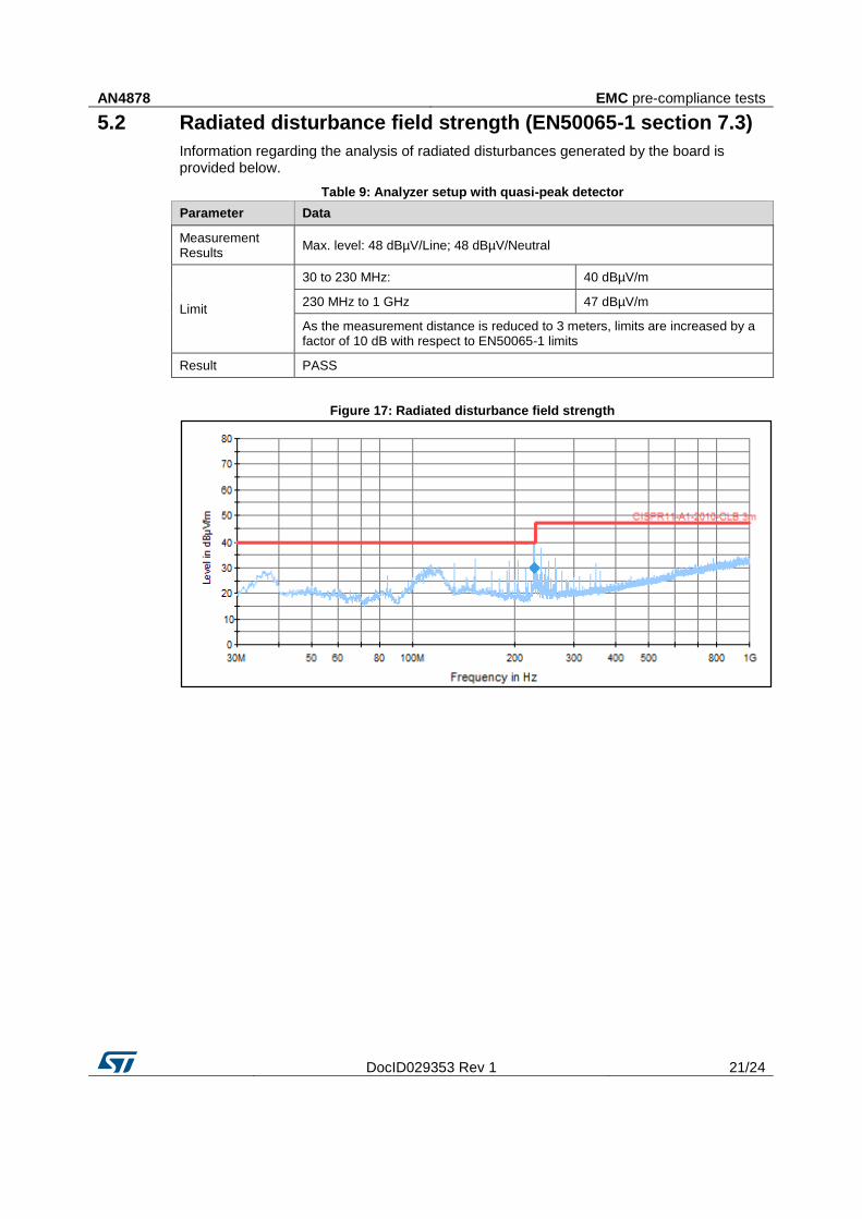
5.2 Radiated disturbance field strength (EN50065-1 section 7.3)
Information regarding the analysis of radiated disturbances generated by the board is provided below.
Table 9: Analyzer setup with quasi-peak detector
Parameter Data
Measurement Results
Max. level: 48 dBµV/Line; 48 dBµV/Neutral
Limit
30 to 230 MHz: 40 dBµV/m
230 MHz to 1 GHz 47 dBµV/m
As the measurement distance is reduced to 3 meters, limits are increased by a factor of 10 dB with respect to EN50065-1 limits
Result PASS
Figure 17: Radiated disturbance field strength
Conclusion AN4878
22/24 DocID029353 Rev 1
6 Conclusion
We have presented a three-output isolated flyback converter reference design for smart meter and power line communication systems, using the VIPER26HD.
The input filter setup, compliance with European standards for smart metering PLC applications and for Electromagnetic compatibility, and overall board performance render it suitable for any power line communication system.
AN4878 Revision history
DocID029353 Rev 1 23/24
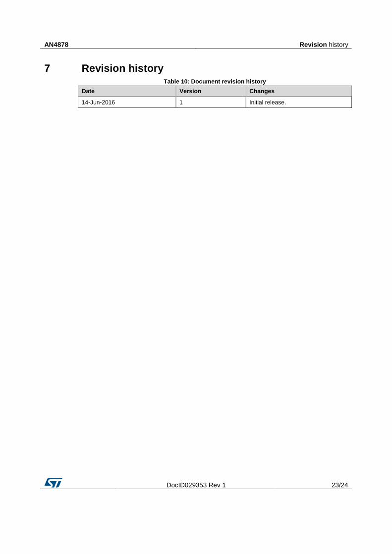
7 Revision history Table 10: Document revision history
Date Version Changes
14-Jun-2016 1 Initial release.
AN4878
24/24 DocID029353 Rev 1
IMPORTANT NOTICE – PLEASE READ CAREFULLY
STMicroelectronics NV and its subsidiaries (“ST”) reserve the right to make changes, corrections, enhancements, modifications , and improvements to ST products and/or to this document at any time without notice. Purchasers should obtain the latest relevant information on ST products before placing orders. ST products are sold pursuant to ST’s terms and conditions of sale in place at the time of order acknowledgement.
Purchasers are solely responsible for the choice, selection, and use of ST products and ST assumes no liability for application assistance or the design of Purchasers’ products.
No license, express or implied, to any intellectual property right is granted by ST herein.
Resale of ST products with provisions different from the information set forth herein shall void any warranty granted by ST for such product.
ST and the ST logo are trademarks of ST. All other product or service names are the property of their respective owners.
Information in this document supersedes and replaces information previously supplied in any prior versions of this document.
© 2016 STMicroelectronics – All rights reserved