Embed Size (px)
Citation preview
State-of-the-Art Graphene High-Frequency ElectronicsYanqing Wu,* Keith A. Jenkins, Alberto Valdes-Garcia, Damon B. Farmer, Yu Zhu, Ageeth A. Bol,Christos Dimitrakopoulos, Wenjuan Zhu, Fengnian Xia, Phaedon Avouris,* and Yu-Ming Lin
IBM Thomas J. Watson Research Center, Yorktown Heights, New York 10598, United States
*S Supporting Information
ABSTRACT: High-performance graphene transistors for radiofrequency applications have received much attention and significantprogress has been achieved. However, devices based on large-areasynthetic graphene, which have direct technological relevance, are stilltypically outperformed by those based on mechanically exfoliatedgraphene. Here, we report devices with intrinsic cutoff frequencyabove 300 GHz, based on both wafer-scale CVD grown graphene andepitaxial graphene on SiC, thus surpassing previous records on anygraphene material. We also demonstrate devices with optimizedarchitecture exhibiting voltage and power gains reaching 20 dB and a wafer-scale integrated graphene amplifier circuit withvoltage amplification.
KEYWORDS: Large-area graphene, radio frequency, voltage gain, power gain, integrated circuit, amplifier
Graphene possesses great potential for radio frequency(RF) applications such as amplifiers and frequency
mixers, whose performance can greatly benefit from the highcarrier velocity of graphene.1−6 Ultrahigh carrier mobility hasbeen demonstrated in mechanically exfoliated flakes underconditions (e.g., suspended graphene at low temperatures) thatminimize external perturbations.7,8 However, technologicallyrelevant graphene devices require large-area synthesizedgraphene1−4 supported on and in contact with a substrate,that is, under conditions where the graphene channels areinevitably affected by extrinsic perturbations. With large-areagraphene becoming available by either CVD or epitaxialmethods,9,10 it is of great importance to build devices fromsuch technologically relevant graphene materials and toevaluate their performance on high-quality substrates likediamond-like carbon (DLC) and silicon carbide (SiC). Here,we demonstrate and discuss RF field-effect transistors (FET)fabricated on wafer-scale CVD and epitaxial graphene, bothachieving record cutoff frequencies surpassing 300 GHz at ascaled channel length of 40 nm. We also conduct a systematicstudy on the voltage gain and power gain of these graphenetransistors and demonstrate significant performance enhance-ments through improvements in graphene quality, choice ofdielectric materials, and the optimal doping of the graphenechannel. Finally, we demonstrate a wafer-scale graphene-based,amplifying integrated circuit, with a gain over 3 dB.Optimizing Devices on CVD and Epitaxial Graphene.
The interfaces between graphene and its substrate, and betweengraphene and its top-gate dielectric insulator, are two dominantsources of scattering in graphene devices. Because of the two-dimensional nature of graphene, scattering at these interfacescan lead to a significant degradation of electrical transport andof the resulting device characteristics. Practical solutions toachieving high quality interfaces must be adopted to maintain
high transistor performance. For example, commonly used SiO2
substrates introduce scattering associated with trap charges andlow-energy surface phonons (59 meV), resulting in deterio-ration of device performance and of performance uniformityacross the wafer. We have previously shown that these effectscan be mitigated by using DLC films as substrates, which areadvantageous because of the high phonon energy in sp3-hybridized carbon (165 meV) and its nonpolar and thenonhydrophilic nature.11 Another desirable substrate is siliconcarbide, which also possesses a high intrinsic phonon energy(116 meV), and high quality graphene sheets can be directlygrown on its surface by epitaxy.1,2 CVD graphene grown on Cufilms and epitaxial graphene grown on SiC are among the twomost practical methods of growing large area graphene.9,10 Inthis study, we demonstrate and investigate graphene devicesfabricated by both approaches.Single layer graphene is grown on copper foils at temper-
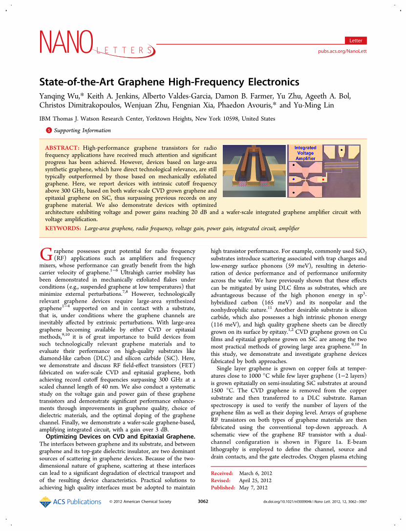
atures close to 1000 °C while few layer graphene (1−2 layers)is grown epitaxially on semi-insulating SiC substrates at around1500 °C. The CVD graphene is removed from the coppersubstrate and then transferred to a DLC substrate. Ramanspectroscopy is used to verify the number of layers of thegraphene film as well as their doping level. Arrays of grapheneRF transistors on both types of graphene materials are thenfabricated using the conventional top-down approach. Aschematic view of the graphene RF transistor with a dual-channel configuration is shown in Figure 1a. E-beamlithography is employed to define the channel, source anddrain contacts, and the gate electrodes. Oxygen plasma etching
Received: March 6, 2012Revised: April 25, 2012Published: May 7, 2012
Letter
pubs.acs.org/NanoLett
© 2012 American Chemical Society 3062 dx.doi.org/10.1021/nl300904k | Nano Lett. 2012, 12, 3062−3067
is used to remove graphene outside the channel regions. Thesource and drain contacts consist of Pd/Au metal stacks.For CVD graphene on DLC, the top-gate dielectric stack
includes an electron-beam evaporated and oxidized Al layerfollowed by an atomic layer deposited (ALD) film of Al2O3.
12
For epitaxial graphene, 15 nm silicon nitride was grown byplasma-enhanced CVD (PECVD) at 400 °C.13 These differentdielectric materials are adopted for CVD and epitaxial graphenerespectively in order to account for the distinct initial doping ofthe graphene prepared by different methods. The doping of as-prepared CVD graphene is typically p-type with a doping levelthat increases in air if no passivation layer is used, while the as-grown epitaxial graphene on SiC is intrinsically n-doped with acarrier concentration of ∼1012−1013 cm−2. These high dopinglevels in as-prepared graphene result in a charge neutrality pointin a graphene transistor far away from zero gate voltage, and asa result, opposite types of external doping need to beimplemented in order to bring the charge neutrality point ofthe graphene transistor back to zero bias. The minimizedchannel doping will greatly improve the transconductance asshown in the Supporting Information and also provide bettercurrent saturation.14 As will be discussed later, the control ofthe doping level in the graphene channel and the correspondingcharge neutrality point are essential for maximizing the voltageand power gain of the graphene FETs. As a result, Al2O3 waschosen as the gate dielectric for CVD graphene because of itselectron doping capability of the graphene channel. Similarly,PECVD silicon nitride was adopted as the gate dielectric for
epitaxial graphene because it provides p-type doping to theoriginally n-doped channel. We note that all fabrication steps,including gate dielectric deposition, involve standard top-down,wafer-compatible approaches that can be readily implementedin high-throughput production.Figure 1b shows a SEM image of a representative dual-
channel graphene RF transistor with a ground−signal−ground(GSG) pad design suitable for RF measurements. The totalwidth of the device is 20 μm. The transmission electronmicroscopy (TEM) images in Figure 1c,f are those of shortchannel devices of CVD graphene on DLC and epitaxialgraphene on SiC, respectively, with channel lengths of 40 nm.Nearly perfect alignment with small ungated regions of lessthan 10 nm is attained in our FETs, which is critical toachieving good device performance and reliable parasitics de-embedding results. High-resolution TEM images in Figure 1d,gshow channel regions of actual devices with monolayer CVDgraphene on DLC and monolayer epitaxial graphene on SiC,respectively, while Figure 1e,h shows the channel regions ofcorresponding open devices where graphene has been etchedaway.
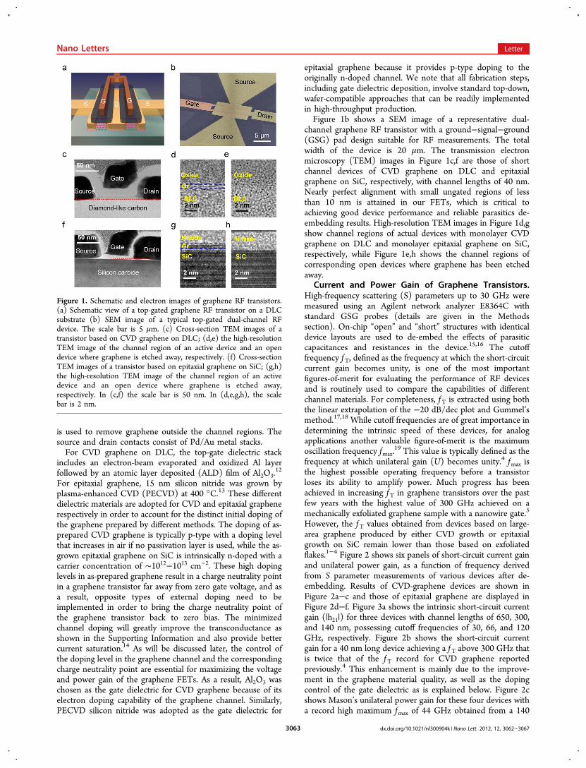
Current and Power Gain of Graphene Transistors.High-frequency scattering (S) parameters up to 30 GHz weremeasured using an Agilent network analyzer E8364C withstandard GSG probes (details are given in the Methodssection). On-chip “open” and “short” structures with identicaldevice layouts are used to de-embed the effects of parasiticcapacitances and resistances in the device.15,16 The cutofffrequency f T, defined as the frequency at which the short-circuitcurrent gain becomes unity, is one of the most importantfigures-of-merit for evaluating the performance of RF devicesand is routinely used to compare the capabilities of differentchannel materials. For completeness, f T is extracted using boththe linear extrapolation of the −20 dB/dec plot and Gummel’smethod.17,18 While cutoff frequencies are of great importance indetermining the intrinsic speed of these devices, for analogapplications another valuable figure-of-merit is the maximumoscillation frequency fmax.
19 This value is typically defined as thefrequency at which unilateral gain (U) becomes unity.4 fmax isthe highest possible operating frequency before a transistorloses its ability to amplify power. Much progress has beenachieved in increasing f T in graphene transistors over the pastfew years with the highest value of 300 GHz achieved on amechanically exfoliated graphene sample with a nanowire gate.5
However, the f T values obtained from devices based on large-area graphene produced by either CVD growth or epitaxialgrowth on SiC remain lower than those based on exfoliatedflakes.1−4 Figure 2 shows six panels of short-circuit current gainand unilateral power gain, as a function of frequency derivedfrom S parameter measurements of various devices after de-embedding. Results of CVD-graphene devices are shown inFigure 2a−c and those of epitaxial graphene are displayed inFigure 2d−f. Figure 3a shows the intrinsic short-circuit currentgain (|h21|) for three devices with channel lengths of 650, 300,and 140 nm, possessing cutoff frequencies of 30, 66, and 120GHz, respectively. Figure 2b shows the short-circuit currentgain for a 40 nm long device achieving a f T above 300 GHz thatis twice that of the f T record for CVD graphene reportedpreviously.4 This enhancement is mainly due to the improve-ment in the graphene material quality, as well as the dopingcontrol of the gate dielectric as is explained below. Figure 2cshows Mason’s unilateral power gain for these four devices witha record high maximum fmax of 44 GHz obtained from a 140
Figure 1. Schematic and electron images of graphene RF transistors.(a) Schematic view of a top-gated graphene RF transistor on a DLCsubstrate (b) SEM image of a typical top-gated dual-channel RFdevice. The scale bar is 5 μm. (c) Cross-section TEM images of atransistor based on CVD graphene on DLC; (d,e) the high-resolutionTEM image of the channel region of an active device and an opendevice where graphene is etched away, respectively. (f) Cross-sectionTEM images of a transistor based on epitaxial graphene on SiC; (g,h)the high-resolution TEM image of the channel region of an activedevice and an open device where graphene is etched away,respectively. In (c,f) the scale bar is 50 nm. In (d,e,g,h), the scalebar is 2 nm.
Nano Letters Letter
dx.doi.org/10.1021/nl300904k | Nano Lett. 2012, 12, 3062−30673063
nm device, which is also a factor of 2 improvement over theprevious record of 20 GHz.4
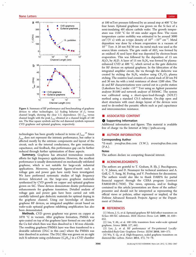
The RF performance of epitaxial graphene grown on SiC hasbeen analyzed in a similar fashion, as shown in Figure 2d−f.The peak f T is also above 300 GHz for 40 nm devices with thehighest value of 350 GHz obtained from the best device. This isalso supported by the dc projection of f T = gm/2πCox, where gmis the transcondutance and Cox is the gate capacitance. Similarto the CVD graphene devices, the peak fmax is about 40 GHzfor a 140 nm device (see Figure 2f). In Figure 5b, we presentthe first systematic study of fmax in graphene transistors basedon large-area synthesized graphene materials. The fmax values of44 and 42 GHz obtained for CVD and epitaxial graphenematerials, respectively, are the highest to date for graphene RFdevices.Voltage Gain for Graphene Transistors. While f T and
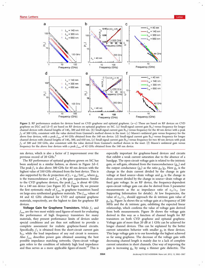
fmax are the two most widely used figures-of-merit for evaluatingthe performance of high frequency transistors for manymaterials, they present performance limits of devices underspecial conditions and are thus not sufficient to provide acomplete assessment for realistic graphene-based circuits.Specifically, f T is obtained from the short-circuit current gainh21, while the load impedance of any real circuit is nonzero.Also fmax describes power gain obtained assuming the bestpossible impedance matching networks. Open-circuit voltagegain refers to the condition of infinitely high load impedanceand thus serves as a more applicable figure-of-merit.19 This is
especially important for graphene-based devices and circuitsthat exhibit a weak current saturation due to the absence of abandgap. The open-circuit voltage gain is related to the intrinsicgain, or self-gain, obtained from the transconductance (gm) andthe output conductance (gd) as the ratio gm/gd. Here gm is thechange in the drain current divided by the change in gatevoltage at fixed source−drain voltage and gd is the change indrain current divided by the change in source−drain voltage atfixed gate voltage. In an RF device, the frequency-dependentopen-circuit voltage gain can also be derived from S parametermeasurements as the ac impedance ratio of z21/z11 (seeSupporting Information for details). At low frequencies, thevalue of z21/z11 should approach the dc intrinsic gain value ofgm/gd. Figure 3a shows the ac voltage gain at a frequency of 200MHz and the dc intrinsic gain, exhibiting the expected linearrelationship, which confirms the value of voltage gain derivedfrom both measurements. Figure 3b shows the voltage gainderived in this way as a function of channel length for RFtransistors on both CVD graphene and epitaxial graphene.Voltage gain of more than 20 dB at 1 GHz can be achieved forlonger channel devices. This can be explained by the bettercurrent saturation behavior with smaller gd in these devices.This large voltage gain is to our knowledge the highest achievedso far using graphene. The decrease of the voltage gain withdecreasing channel length is mainly due to a lack of completecurrent saturation in short channels. One way of improving thegain is increasing gm by using a thinner gate dielectric. The
Figure 2. RF performance analysis for devices based on CVD graphene and epitaxial graphene. (a−c) These are based on RF devices on CVDgraphene on DLC and (d−f) are based on RF devices on epitaxial graphene on SiC. (a) Small-signal current gain |h21| versus frequency for longerchannel devices with channel lengths of 140,, 300 and 650 nm. (b) Small-signal current gain |h21| versus frequency for the 40 nm device with a peakf T of 300 GHz, consistent with the value derived from Gummel’s method shown in the inset. (c) Mason’s unilateral gain versus frequency for theabove four devices, with a peak fmax of 44 GHz obtained from the 140 nm device. (d) Small-signal current gain |h21| versus frequency for longerchannel devices with channel lengths of 140,, 300, and 650 nm, (e) Small-signal current gain |h21| versus frequency for two 40 nm devices with peakf T of 300 and 350 GHz, also consistent with the value derived from Gummel’s method shown in the inset. (f) Mason’s unilateral gain versusfrequency for the above four devices with a peak fmax of 42 GHz obtained from the 140 nm device.
Nano Letters Letter
dx.doi.org/10.1021/nl300904k | Nano Lett. 2012, 12, 3062−30673064
resulting larger gate capacitance will not only increase gm, butalso help reduce gd by improving the electro-static gate control.In Figure 3c, we show an improvement in voltage gain of over15 dB by scaling the EOT from 20 to 3 nm. This illustrates therole of the dielectric thickness and points out a possible way tofurther improve voltage gain, especially in shorter channeldevices.Wafer-Scale Graphene Amplifier Integrated Circuit.
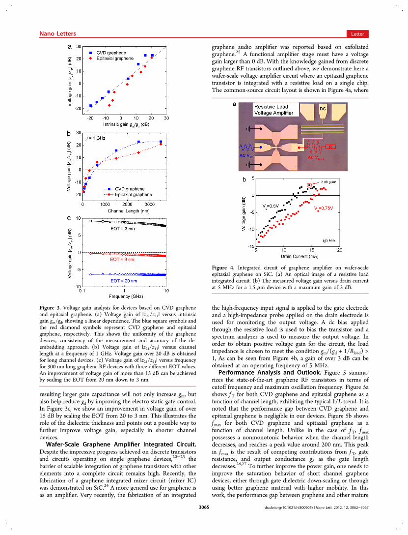
Despite the impressive progress achieved on discrete transistorsand circuits operating on single graphene devices,20−23 thebarrier of scalable integration of graphene transistors with otherelements into a complete circuit remains high. Recently, thefabrication of a graphene integrated mixer circuit (mixer IC)was demonstrated on SiC.24 A more general use for graphene isas an amplifier. Very recently, the fabrication of an integrated
graphene audio amplifier was reported based on exfoliatedgraphene.25 A functional amplifier stage must have a voltagegain larger than 0 dB. With the knowledge gained from discretegraphene RF transistors outlined above, we demonstrate here awafer-scale voltage amplifier circuit where an epitaxial graphenetransistor is integrated with a resistive load on a single chip.The common-source circuit layout is shown in Figure 4a, where
the high-frequency input signal is applied to the gate electrodeand a high-impedance probe applied on the drain electrode isused for monitoring the output voltage. A dc bias appliedthrough the resistive load is used to bias the transistor and aspectrum analyzer is used to measure the output voltage. Inorder to obtain positive voltage gain for the circuit, the loadimpedance is chosen to meet the condition gm/(gd + 1/Rload) >1, As can be seen from Figure 4b, a gain of over 3 dB can beobtained at an operating frequency of 5 MHz.
Performance Analysis and Outlook. Figure 5 summa-rizes the state-of-the-art graphene RF transistors in terms ofcutoff frequency and maximum oscillation frequency. Figure 5ashows f T for both CVD graphene and epitaxial graphene as afunction of channel length, exhibiting the typical 1/L trend. It isnoted that the performance gap between CVD graphene andepitaxial graphene is negligible in our devices. Figure 5b showsfmax for both CVD graphene and epitaxial graphene as afunction of channel length. Unlike in the case of f T, fmaxpossesses a nonmonotonic behavior when the channel lengthdecreases, and reaches a peak value around 200 nm. This peakin fmax is the result of competing contributions from f T, gateresistance, and output conductance gd as the gate lengthdecreases.26,27 To further improve the power gain, one needs toimprove the saturation behavior of short channel graphenedevices, either through gate dielectric down-scaling or throughusing better graphene material with higher mobility. In thiswork, the performance gap between graphene and other mature
Figure 3. Voltage gain analysis for devices based on CVD grapheneand epitaxial graphene. (a) Voltage gain of |z21/z11| versus intrinsicgain gm/gd, showing a linear dependence. The blue square symbols andthe red diamond symbols represent CVD graphene and epitaxialgraphene, respectively. This shows the uniformity of the graphenedevices, consistency of the measurement and accuracy of the de-embedding approach. (b) Voltage gain of |z21/z11| versus channellength at a frequency of 1 GHz. Voltage gain over 20 dB is obtainedfor long channel devices. (c) Voltage gain of |z21/z11| versus frequencyfor 300 nm long graphene RF devices with three different EOT values.An improvement of voltage gain of more than 15 dB can be achievedby scaling the EOT from 20 nm down to 3 nm.
Figure 4. Integrated circuit of graphene amplifier on wafer-scaleepitaxial graphene on SiC. (a) An optical image of a resistive loadintegrated circuit. (b) The measured voltage gain versus drain currentat 5 MHz for a 1.5 μm device with a maximum gain of 3 dB.
Nano Letters Letter
dx.doi.org/10.1021/nl300904k | Nano Lett. 2012, 12, 3062−30673065
technologies has been greatly reduced in terms of fmax.19 Since
fmax does not represent the intrinsic performance, but rather isaffected mostly by the extrinsic components and layout of thecircuit, such as the internal conductance, the gate resistance,capacitance, and feedback, this performance gap can be furtherreduced through further optimization of these aspects.Summary. Graphene has attracted tremendous research
efforts for high frequency applications. However, the excellentperformance is usually demonstrated on mechanically exfoliatedgraphene, which is not suitable for large-scale industrialapplications. Moreover, important figures-of-merit such asvoltage gain and power gain have rarely been investigated.We have performed systematic studies of high frequencydevices fabricated on the large-area graphene materialssynthesized by CVD growth on copper and epitaxial graphenegrown on SiC. These devices demonstrate drastic performanceenhancements for graphene transistors. Detailed analysis ofvoltage gain and power gain have been carried out withcarefully tailored gate dielectric materials for optimal doping inthe graphene channel. Using our knowledge of discretegraphene RF devices, an integrated amplifier circuit based onwafer-scale epitaxial graphene exhibiting amplification has alsobeen demonstrated.Methods. CVD grown graphene was grown on copper at
1070 °C in vacuum. After graphene formation, PMMA wasspin-coated on top of the graphene layer formed on one side ofthe Cu foil which then was then dissolved in 1 M iron chloride.The resulting graphene/PMMA layer was then transferred to adesirable substrate (DLC in this case) where the PMMA waslater dissolved in acetone. The DLC film was grown on an eightinch Si substrate using cyclohexane (C6H12) in a CVD chamber
at 100 mTorr pressure followed by an anneal step at 400 °C forfour hours. Epitaxial graphene was grown on the Si face of asemi-insulating 4H silicon carbide wafer. The growth temper-ature was 1550 °C for 10 min under argon flow. The roomtemperature carrier mobility was estimated to be around 3000cm2/(V s) with an n-type density of 1012 −1013 cm−2. Metaldeposition was done by e-beam evaporation in a vacuum of10−7 Torr. A 20 nm Pd/30 nm Au metal stack was used as thesource/drain contacts. The gate oxide of AlOx was formed byan oxidized Al seed layer that was deposited by electron-beamevaporation. This was followed by the deposition of 15 nmAl2O3 by ALD. A layer of 15 nm Si3N4 was formed by plasma-enhanced CVD at 400 °C, which served as the gate dielectricfor RF devices on epitaxial graphene. In the fabrication of theintegrated amplifier circuit, the via through the dielectric wascreated by etching the Si3N4 window using CF4/O2 plasmaetching. The resistive load consists of a metal stack of 20 nm Pdand 30 nm Au with a total resistance of about 1200 ohm. Thedc and RF characterizations were carried out in a probe station(Lakeshore Inc.) under <10−6 Torr using an Agilent parameteranalyzer B1500 and network analyzer of E8364C. The systemwas calibrated using a short-open-load-through (SOLT)method using a standard CS-5 substrate. On-chip open andshort structures with exact design layout of the devices wereused to de-embed the parasitic effects such as pad capacitanceand interconnection resistance.
■ ASSOCIATED CONTENT
*S Supporting InformationAdditional information and figures. This material is availablefree of charge via the Internet at http://pubs.acs.org.
■ AUTHOR INFORMATION
Corresponding Author*E-mail: [email protected] (Y.W.); [email protected](P.A.).
NotesThe authors declare no competing financial interest.
■ ACKNOWLEDGMENTSThe authors are grateful to T. Graham, B. Ek, J. Bucchignano,C. V. Jahnes, and D. Neumayer for technical assistance and A.Grill, C. Y. Sung, M. Freitag, and V. Perebeinos for discussions.The authors would also like to thank DARPA for partialfinancial support through the CERA program (contractFA8650-08-C-7838). The views, opinions, and/or findingscontained in this article/presentation are those of the author/presenter and should not be interpreted as representing theofficial views or policies, either expressed or implied, of theDefense Advanced Research Projects Agency or the Depart-ment of Defense.
■ REFERENCES(1) Moon, J. S.; et al. Epitaxial-graphene RF field-effect transistors onSi-face 6H-SiC substrates. IEEE Electron Device Lett. 2009, 30, 650−652.(2) Lin, Y.-M.; et al. 100 GHz transistors from wafer-scale epitaxialgraphene. Science 2010, 327, 662.(3) Lee, J.; et al. RF performance of Pre-patterned Locally-embedded-Back-Gate Graphene Device. IEDM 2010, 568−571.(4) Wu, Y. Q.; et al. High-frequency, scaled graphene transistors ondiamond-like carbon. Nature 2011, 472, 74−78.
Figure 5. Summary of RF performance and benchmarking of graphenedevices to other technologies. (a) Scaling behavior of f T versuschannel length, showing the clear 1/L dependence. (b) fmax versuschannel length with the peak fmax obtained at a channel length of 140nm. The blue square symbols and the red diamond symbols representCVD graphene and epitaxial graphene, respectively.
Nano Letters Letter
dx.doi.org/10.1021/nl300904k | Nano Lett. 2012, 12, 3062−30673066
(5) Liao, L.; et al. High-speed graphene transistors with a self-alignednanowire gate. Nature 2010, 467, 305−308.(6) Meric, I.; Baklitskaya, N.; Kim, P.; Shepard, K. L. RF performanceof top-gated graphene field-effect transistors. IEDM 2008,DOI: 4796738.(7) Bolotin, K. I.; et al. Ultrahigh electron mobility in suspendedgraphene. Solid State Commun. 2008, 146, 351−355.(8) Du, X.; Skachko, I.; Barker, A.; Andrei, E. Y. Approaching ballistictransport in suspended graphene. Nat. Nanotechnol. 2008, 3, 491−495.(9) Berger, C.; et al. Electronic Confinement and Coherence inPatterned Epitaxial Graphene. Science 2006, 312, 1191.(10) Li, X. S.; et al. Large-Area Synthesis of High-Quality andUniform Grapene Films on Copper Foils. Science 2009, 324, 1312−1314.(11) Balandin, A. A. Thermal properties of graphene andnanostructured carbon materials. Nat. Mater. 2011, 10, 569−581.(12) Kim, S.; et al. Realization of a high mobility dual-gated graphenefield-effect transistor with Al2O3 dielectric. Appl. Phys. Lett. 2009, 94,062107.(13) Zhu, W. J.; Neumayer, D.; Perebeinos, V.; Avouris, Ph. SiliconNitride Gate Dielectrics and Band Gap Engineering in GrapheneLayers. Nano Lett. 2010, 10, 3572−3576.(14) Wu, Y.; et al. Three-Terminal Graphene Negative DifferentialResistance Devices. ACS Nano 2012, 6 (3), 2610−2616.(15) Koolen, M. C. A. M.; Geelen, J. A. M.; Versleijen, M. P. J. G. Animproved deembedding technique for on-wafer high-frequencycharacterization. Proc. Bipolar Circuits Technol. Meet. 1991, 191−194.(16) Cheng, Y.; Deen, M. J.; Chen, C.-H. MOSFET modeling for RFIC design. IEEE Trans. Electron Devices 2005, 52, 1286−1303.(17) Kim, D. H.; del Alamo, J. A. 30-nm InAs pseudomorphicHEMTs on an InP substrate with a current-gain cutoff frequency of628 GHz. IEEE Electron Device Lett. 2008, 29, 830−833.(18) Gummel, H. K. On the definition of the cutoff frequency f T.Proc. IEEE 1969, 57, 2159.(19) Schwierz, F. Graphene transistors. Nat. Nanotechnol. 2010, 5,487−496.(20) Han, S.-J.; et al. High-frequency graphene voltage amplifier.Nano Lett. 2011, 11, 3690−3693.(21) Yang, X.; Liu, G.; Balandin, A. A.; Mohanram, K. Triple-modesingle transistor graphene amplifier and its applications. ACS Nano2010, 4, 5532−5538.(22) Liao, L.; et al. Scalable fabrication of self-aligned graphenetransistors and circuits on glass. Nano Lett. 2011, DOI: 10.1021/nl201922c.(23) Wang, H.; Hsu, A.; Wu, J.; Kong, J.; Palacios, T. Graphene-based ambipolar RF mixers. IEEE Electron Device Lett. 2009, 31, 906−908.(24) Lin, Y.-M.; et al. Wafer-scale graphene integrated circuit. Science2011, 332, 1294−1297.(25) Guerriero, E.; Polloni, L.; Rizzi, L. G.; Bianchi, M.; Mondello,G.; Sordan, R. Graphene Audio Voltage Amplifier. Small 2011,DOI: 10.1002/smll.201102141.(26) Lee, T. H. The Design of CMOS Radio-Frequency integratedCircuits; Cambridge University Press: New York, 2004.(27) Sze, S. M.; Ng, K. K. Physics of Semiconductor Devices, 3rd ed.;Wiley-Interscience: New York, 2006.
Nano Letters Letter
dx.doi.org/10.1021/nl300904k | Nano Lett. 2012, 12, 3062−30673067


![Graphene and 2D Electronics [for a general "curious" audience]](https://img.pdfslide.us/doc/110x75/557d7944d8b42a2c428b4cd0/graphene-and-2d-electronics-for-a-general-curious-audience.jpg)


![presentation-14-ver3.pptx [Last saved by user]vpopov/Grapnene-properties-and... · 2019-09-20 · Graphene production Graphene dot, flakes, ribbons, sheets…: graphene electronics-Mechanical](https://img.pdfslide.us/doc/110x75/5ecb767a0746fe023043a7c7/presentation-14-ver3pptx-last-saved-by-user-vpopovgrapnene-properties-and.jpg)