Embed Size (px)
Citation preview
MR45CH16-Hong ARI 28 March 2015 12:58
RE V I E W
S
IN
AD V A
NC
E
Materials for Flexible,Stretchable Electronics:Graphene and 2D MaterialsSang Jin Kim,∗ Kyoungjun Choi,∗ Bora Lee, Yuna Kim,and Byung Hee Hong§
Department of Chemistry, College of Natural Sciences, Seoul National University, Seoul,151-747, Republic of Korea; email: [email protected]
Annu. Rev. Mater. Res. 2015. 45:16.1–16.22
The Annual Review of Materials Research is online atmatsci.annualreviews.org
This article’s doi:10.1146/annurev-matsci-070214-020901
Copyright c© 2015 by Annual Reviews.All rights reserved
∗These authors contributed equally to thismanuscript.
§Corresponding author
Keywords
graphene, 2D materials, flexible electronics, transparent electrode
Abstract
Recently, 2D materials have been intensively studied as emerging materialsfor future electronics, including flexible electronics, photonics, and electro-chemical energy storage devices. Among representative 2D materials (suchas graphene, boron nitride, and transition metal dichalcogenides) that exhibitextraordinary properties, graphene stands out in the flexible electronics fielddue to its combination of high electron mobility, high thermal conductivity,high specific surface area, high optical transparency, excellent mechanicalflexibility, and environmental stability. This review covers the synthesis,transfer, and characterization methods of graphene and 2D materials andgraphene’s application to flexible devices as well as comparison with othercompeting materials.
16.1
Review in Advance first posted online on April 9, 2015. (Changes may still occur before final publication online and in print.)
Changes may still occur before final publication online and in print
Ann
u. R
ev. M
ater
. Res
. 201
5.45
. Dow
nloa
ded
from
ww
w.a
nnua
lrev
iew
s.or
g A
cces
s pr
ovid
ed b
y H
arva
rd U
nive
rsity
on
04/1
4/15
. For
per
sona
l use
onl
y.
MR45CH16-Hong ARI 28 March 2015 12:58
1. INTRODUCTION
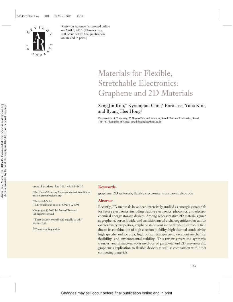
Future electronics technology will evolve from rigid devices to bendable/rollable/foldable devicesthat are wearable like clothes or accessories (Figure 1) (1). These flexible devices will be advan-tageous over rigid ones due to their better durability, lighter weight, higher space efficiency, andimproved comfort, but the development of such devices requires breakthroughs in materials be-cause they will require flexibility as well as desirable electrical insulating/semiconducting/metallicproperties. Traditional device fabrication processes have been limited mostly to rigid substratesand vacuum deposition methods. However, recently emerging 2D materials such as graphene,boron nitride (BN), and transition metal dichalcogenides (TMDCs) are attractive because of theiroutstanding electrical, optical, and mechanical properties, which are ideal for flexible and stretch-able electronics.
Graphene not only exhibits excellent optoelectronic and mechanical properties but also canexhibit good adhesion with several organic materials so as to produce high-performance organicfield-effect transistors (FETs), organic light-emitting diodes (OLEDs), and organic photovoltaiccells (OPVs). The high specific surface-to-volume ratio of graphene and its excellent chemicalstability are also expected to be useful for higher-performance power storage devices by optimizingchemical functionalization and doping processes. However, the etching methods used to removegraphene from catalytic substrates and its transfer will be as important as the synthesis of high-quality, large-area, defect-free material by chemical vapor deposition (CVD). Through theseprocesses, the overall quality of graphene can be optimized to be used for flexible electronics, asreviewed below.
2. METHODS FOR GRAPHENE SYNTHESIS AND TRANSFER
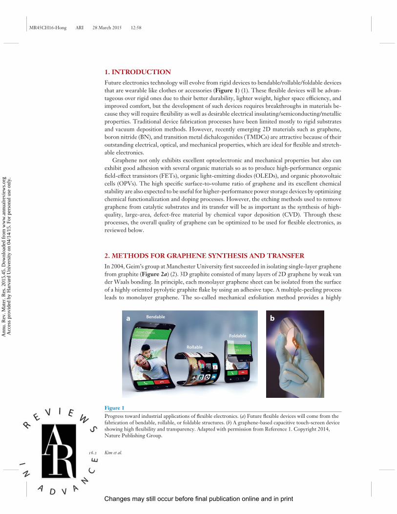
In 2004, Geim’s group at Manchester University first succeeded in isolating single-layer graphenefrom graphite (Figure 2a) (2). 3D graphite consisted of many layers of 2D graphene by weak vander Waals bonding. In principle, each monolayer graphene sheet can be isolated from the surfaceof a highly oriented pyrolytic graphite flake by using an adhesive tape. A multiple-peeling processleads to monolayer graphene. The so-called mechanical exfoliation method provides a highly
a Bendable
Rollable
Foldable
b
Figure 1Progress toward industrial applications of flexible electronics. (a) Future flexible devices will come from thefabrication of bendable, rollable, or foldable structures. (b) A graphene-based capacitive touch-screen deviceshowing high flexibility and transparency. Adapted with permission from Reference 1. Copyright 2014,Nature Publishing Group.
16.2 Kim et al.
Changes may still occur before final publication online and in print
Ann
u. R
ev. M
ater
. Res
. 201
5.45
. Dow
nloa
ded
from
ww
w.a
nnua
lrev
iew
s.or
g A
cces
s pr
ovid
ed b
y H
arva
rd U
nive
rsity
on
04/1
4/15
. For
per
sona
l use
onl
y.
MR45CH16-Hong ARI 28 March 2015 12:58
20 μm 5 nm 5 μm
3 layers
0.34 nm
Bilayer
20 nma db c
1 μm
1 nm
Figure 2Graphene films produced by various methods. (a) Photograph of a multilayer graphene flake isolated from bulk graphite by using themechanical exfoliation method with adhesive tape. Panel a adapted with permission from Reference 2. Copyright 2004, AmericanAssociation for the Advancement of Science. (b) AFM image of graphite oxide sheets deposited onto a mica substrate from an aqueousdispersion (inset) obtained by the chemical exfoliation method. Panel b adapted with permission from Reference 10. Copyright 2006,Nature Publishing Group. (c) STM topographs of epitaxial graphene on silicon carbide (SiC) (0001) show large flatness. Panel c adaptedwith permission from Reference 15. Copyright 2007, Elsevier. (d ) SEM (left) and TEM (right) images of graphene films on Ni layersgrown by the chemical vapor deposition method. Panel d adapted with permission from Reference 24. Copyright 2009, NaturePublishing Group.
crystalline structure of graphene with outstanding electrical properties such as the ambipolar fieldeffect (2), the quantum Hall effect at room temperature (3–7), and extremely high carrier mobilityfor fundamental studies (8, 9). However, this method is limited by the size of the graphite flakesavailable (typically micrometer in size). Furthermore, the thickness is difficult to accurately control,resulting in a low-yield problem, and so this is an unsuitable technique for mass production.
Ruoff ’s group demonstrated a solution-based process for obtaining single-layer graphene bychemical exfoliation (Figure 2b) (10–13). The chemical exfoliation method uses strong acids andoxidants to obtain a sheet of graphene oxide (GO) from graphite powder dispersed in solution.This method can introduce structural and electrical disorder in the graphene during the oxidationprocess, and so an additional process was needed to enhance the electrical property of GO due tooxygen-rich functional groups on GO’s surface. Reduced graphene oxide (RGO) films have goodconducting properties, which can be obtained by treating GO films with reducing agents such ashydrazine or hydrothermal annealing. Although chemical exfoliation is a simple, solution-basedprocess and can produce large quantities of graphene at low cost, the electrical and optical prop-erties of RGO films are inferior to those of the graphene film obtained by mechanical exfoliationor CVD methods.
The epitaxial growth process is another possible method that allows for the production ofhigh-quality and large-area single layers and multilayers of graphene on silicon carbide (SiC)(0001) in high vacuum and high temperature (∼1,000–1,600◦C). In this process, Si is sublimated,leaving carbon behind (Figure 2c) (14–16) on the surface of the SiC. SiC wafers can be utilized asa substrate for graphene electronic devices because SiC is a wide-band-gap material but is rigid.Although graphene grown by the epitaxial process has outstanding electrical properties, enablingit to be utilized in high-frequency (∼100-GHz) electrical devices (17), SiC substrates are relativelyexpensive and limited in size. It is also difficult to transfer graphene grown in this way onto otherarbitrary substrates for commercial adoption.
Graphene has also been grown by the thermal chemical vapor deposition (T-CVD) method,which consists of decomposition of hot hydrocarbon sources on catalytic surfaces or surface
www.annualreviews.org • Materials for Flexible, Stretchable Electronics 16.3
Changes may still occur before final publication online and in print
Ann
u. R
ev. M
ater
. Res
. 201
5.45
. Dow
nloa
ded
from
ww
w.a
nnua
lrev
iew
s.or
g A
cces
s pr
ovid
ed b
y H
arva
rd U
nive
rsity
on
04/1
4/15
. For
per
sona
l use
onl
y.
MR45CH16-Hong ARI 28 March 2015 12:58
segregation of carbon during a cooling step from the carbon/metal binary phase system. Car-bon sources, such as CH4, C2H2, or solid sources [polystyrene, polyacrylonitrile, polymethylmethacrylate (PMMA) polymers], and various transition metal catalysts (Cu, Ni, Pd, Ru, Ir, oralloys) have been used for graphene growth by T-CVD (18–27). Growth conditions such as thetemperature dependence of carbon solubility in the metal and the gas flow rate and pressure de-termine the morphology (domain size and boundaries) and quality of graphene films grown bythe T-CVD method.
In 2009, our group reported the growth of graphene on polycrystalline Ni thin films and showedhigh electron mobility [up to 3,650 cm2/(V·s) of carrier mobility] (Figure 2d ) (24). However,graphene grown on Ni thin films consists of a mixture of both single layers and multilayers becausethe thickness control of graphene on a Ni surface depends on the rapid cooling condition of themetal carbide state. Due to the very low carbon solubility in Cu, the Cu catalyst is favored to obtainhigh-quality, uniform, and single-layer-dominant (>95%) graphene. The scale of graphene grownon Cu ranges from 30 inches (28) to 100 m (29). Unfortunately, the T-CVD process requires veryhigh temperatures (>1,000◦C) and is not suitable for mass production. Plasma-assisted CVDmethods overcome this limitation of T-CVD by using combined thermal and plasma energy,which facilitates the decomposition of hydrocarbon at lower temperatures (<1,000◦C) (30–33).The electrical and optical properties of graphene films grown using plasma-assisted CVD werecontrolled by varying the plasma power, growth time, and growth temperature.
A graphene film is extremely thin and easy to tear during the catalyst etching and transferprocesses. Therefore, to reduce defects produced during the transfer process to a suitable targetsubstrate, as-grown graphene films need a polymer supporting layer. One method, the wet-transfermethod, uses spin-coated PMMA or polydimethylsiloxane (PDMS) as a supporting and protectivelayer (34). In contrast, in dry-transfer methods, the use of thermal release tape allows for large-areagraphene transfer onto flexible polymers and rigid substrates without being limited in size (28,35). Multiple stacking methods are also used to enhance the electrical conductivity of graphenefilms through the layer-by-layer printing process (36–38). Refinement of direct deposition andtransfer methods of graphene onto insulating substrates will be key to replacing indium tin oxide(ITO) as the ubiquitous transparent conductor (39–41).
3. OPTIMIZING PROPERTIES FOR FLEXIBLEAND STRETCHABLE DEVICES
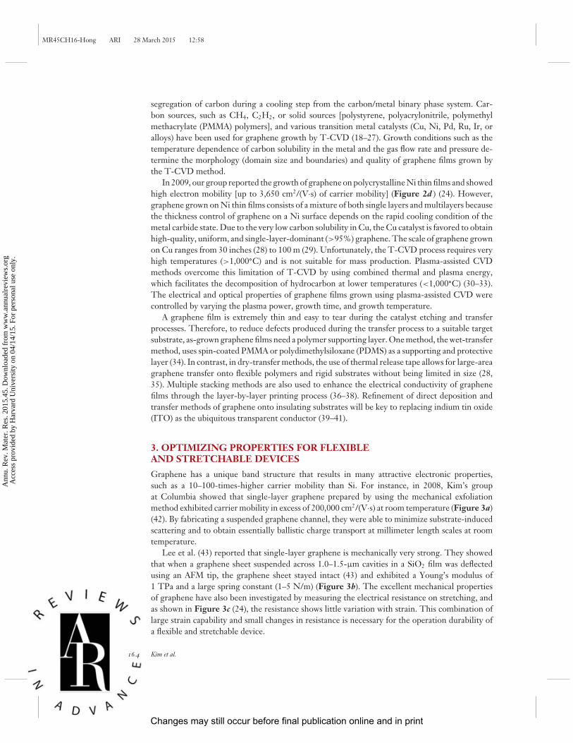
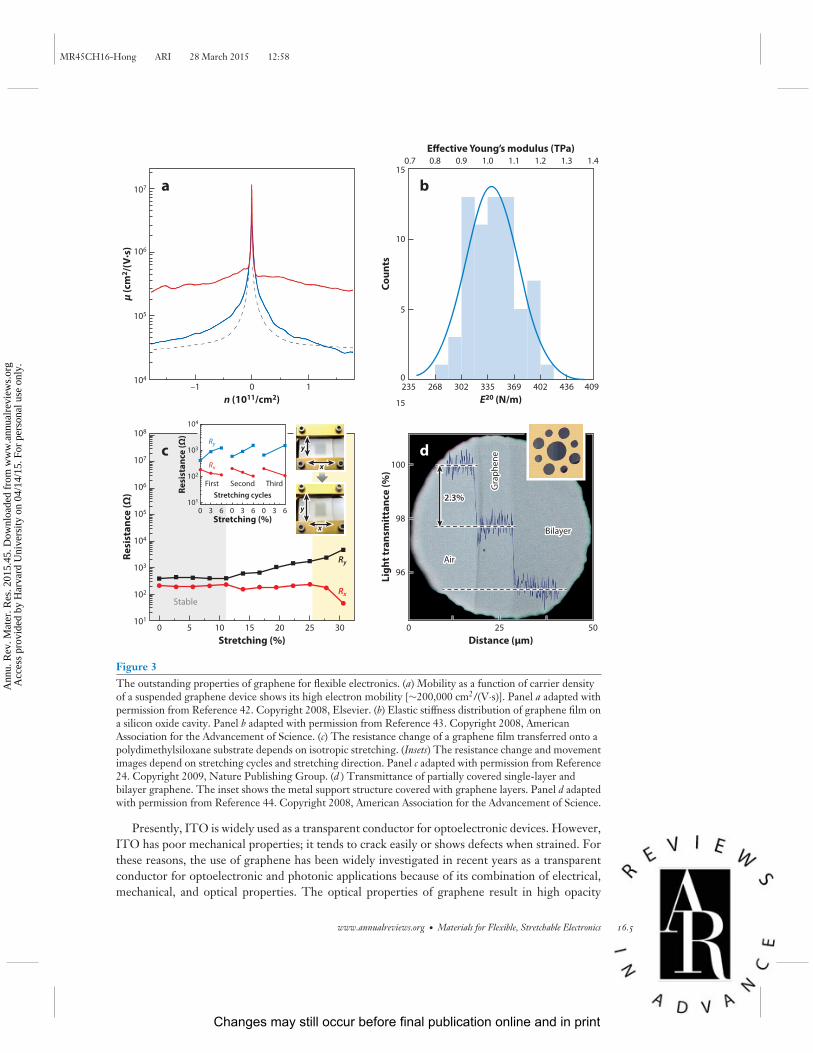
Graphene has a unique band structure that results in many attractive electronic properties,such as a 10–100-times-higher carrier mobility than Si. For instance, in 2008, Kim’s groupat Columbia showed that single-layer graphene prepared by using the mechanical exfoliationmethod exhibited carrier mobility in excess of 200,000 cm2/(V·s) at room temperature (Figure 3a)(42). By fabricating a suspended graphene channel, they were able to minimize substrate-inducedscattering and to obtain essentially ballistic charge transport at millimeter length scales at roomtemperature.
Lee et al. (43) reported that single-layer graphene is mechanically very strong. They showedthat when a graphene sheet suspended across 1.0–1.5-μm cavities in a SiO2 film was deflectedusing an AFM tip, the graphene sheet stayed intact (43) and exhibited a Young’s modulus of1 TPa and a large spring constant (1–5 N/m) (Figure 3b). The excellent mechanical propertiesof graphene have also been investigated by measuring the electrical resistance on stretching, andas shown in Figure 3c (24), the resistance shows little variation with strain. This combination oflarge strain capability and small changes in resistance is necessary for the operation durability ofa flexible and stretchable device.
16.4 Kim et al.
Changes may still occur before final publication online and in print
Ann
u. R
ev. M
ater
. Res
. 201
5.45
. Dow
nloa
ded
from
ww
w.a
nnua
lrev
iew
s.or
g A
cces
s pr
ovid
ed b
y H
arva
rd U
nive
rsity
on
04/1
4/15
. For
per
sona
l use
onl
y.
MR45CH16-Hong ARI 28 March 2015 12:58
0
n (1011/cm2)
µ (c
m2/(
V·s
)
104
105
106
107
369 402 436 409235 268 302 335
E20 (N/m)
Co
un
ts
15
10
5
0
1.1 1.2 1.3 1.40.7 0.8 0.9 1.0
Effective Young’s modulus (TPa)
–1 1
a b
15 20 3010
Stretching (%)
Re
sist
an
ce (
Ω)
101
105
Rx
2.3%2.3%
Ry
107
102
103
104
106
108
25 500
Distance (μm)
Lig
ht
tra
nsm
itta
nce
(%
)
15
100
98
96
5
Stable
AirAir
BilayerBilayer
Gra
ph
en
eG
rap
he
ne
0 25
c d
Re
sist
an
ce (
Ω)
101
0 3 6 0 3Stretching (%)
Stretching cycles
SecondFirst
Rx
Ry
Third
6 0 3 6
102
103
104
yy
xx
yy
xx
Figure 3The outstanding properties of graphene for flexible electronics. (a) Mobility as a function of carrier densityof a suspended graphene device shows its high electron mobility [∼200,000 cm2/(V·s)]. Panel a adapted withpermission from Reference 42. Copyright 2008, Elsevier. (b) Elastic stiffness distribution of graphene film ona silicon oxide cavity. Panel b adapted with permission from Reference 43. Copyright 2008, AmericanAssociation for the Advancement of Science. (c) The resistance change of a graphene film transferred onto apolydimethylsiloxane substrate depends on isotropic stretching. (Insets) The resistance change and movementimages depend on stretching cycles and stretching direction. Panel c adapted with permission from Reference24. Copyright 2009, Nature Publishing Group. (d ) Transmittance of partially covered single-layer andbilayer graphene. The inset shows the metal support structure covered with graphene layers. Panel d adaptedwith permission from Reference 44. Copyright 2008, American Association for the Advancement of Science.
Presently, ITO is widely used as a transparent conductor for optoelectronic devices. However,ITO has poor mechanical properties; it tends to crack easily or shows defects when strained. Forthese reasons, the use of graphene has been widely investigated in recent years as a transparentconductor for optoelectronic and photonic applications because of its combination of electrical,mechanical, and optical properties. The optical properties of graphene result in high opacity
www.annualreviews.org • Materials for Flexible, Stretchable Electronics 16.5
Changes may still occur before final publication online and in print
Ann
u. R
ev. M
ater
. Res
. 201
5.45
. Dow
nloa
ded
from
ww
w.a
nnua
lrev
iew
s.or
g A
cces
s pr
ovid
ed b
y H
arva
rd U
nive
rsity
on
04/1
4/15
. For
per
sona
l use
onl
y.
MR45CH16-Hong ARI 28 March 2015 12:58
for an atomic monolayer. The transmittance of graphene decreases approximately 2.3% witheach layer as the number of graphene layers increases (Figure 3d ) (44). Furthermore, graphenefilms transferred onto flexible polyethylene terephthalate (PET) and stretchable PDMS substratesmaintain their high transparency and flexible properties (34).
The adsorption of various molecules on the graphene surface is possible because of graphene’shydrophobic surface, which is similar to that of carbon nanotubes (CNTs). Also, the conductivityand doping types can be modified by chemical treatment. There are now numerous reports ofdoping methods such as modification of the substrate surface with self-assembled monolayers (45,46); sp3 functionalization of carbon with H, F, or Cl (47); atomic substitution with N (48, 49); andsurface treatment of graphene by using certain molecules (50–52) or acidic solutions (37).
4. APPLICATIONS FOR FLEXIBlE AND STRETCHABLE ELECTRONICS
4.1. Graphene-Based Electronics
Future electronics are more flexible and stretchable than traditional ones. Rare mineral resourcesshow outstanding electrical properties, but they are suitable for rigid components. Graphene andgraphene deviates have emerged as promising materials for flexible and stretchable electronics.
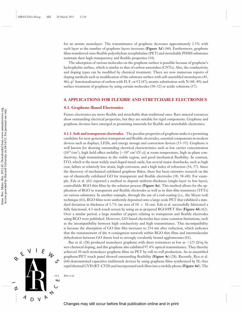
4.1.1. Soft and transparent electrodes. The peculiar properties of graphene make it a promisingcandidate for next-generation transparent and flexible electrodes, essential components in moderndevices such as displays, LEDs, and energy storage and conversion devices (53–55). Graphene iswell known for showing outstanding electrical characteristics such as low carrier concentration(1013/cm2), high field-effect mobility [∼104 cm2/(V·s)] at room temperature, high in-plane con-ductivity, high transmittance in the visible region, and good mechanical flexibility. In contrast,ITO, which is the most widely used doped metal oxide, has several major drawbacks, such as highcost, failure at relatively low strain, high corrosion, and a high index of refraction (56, 57). Sincethe discovery of mechanical exfoliated graphene flakes, there has been extensive research on theuse of chemically exfoliated GO for transparent and flexible electrodes (38, 58–60). For exam-ple, Eda et al. (61) reported a method to deposit uniform-thickness (single-layer to few-layer),controllable RGO thin films by the solution process (Figure 4a). This method allows for the ap-plication of RGO in transparent and flexible electrodes as well as in thin-film transistors (TFTs)on various substrates. In another example, through the use of a rod-coating (i.e., the Meyer rod)technique (61), RGO films were uniformly deposited onto a large-scale PET that exhibited a stan-dard deviation in thickness of 3.7% (an area of 10 × 10 cm). Eda et al. successfully fabricated afully functional, 4.5-inch touch screen by using an as-prepared RGO/PET film (Figure 4b) (62).Over a similar period, a large number of papers relating to transparent and flexible electrodesusing RGO were published. However, GO-based electrodes face some common limitations, suchas the incompatibility between high conductivity and high transmittance. This incompatibilityis because the absorption of GO thin film increases to 254 nm after reduction, which indicatesthat the reinstatement of the π-conjugation network within RGO thin films and intermoleculardehydration between GO sheets lead to strongly covalently bound agglomerates (63).
Bae et al. (28) produced monolayer graphene with sheet resistances as low as ∼125 �/sq bywet-chemical doping, and this graphene also exhibited 97.4% optical transmittance. They therebyachieved 30-inch monolayer graphene films on PET by roll-to-roll production. An as-assembledgraphene/PET touch panel showed outstanding flexibility (Figure 4c) (28). Recently, Ryu et al.(64) demonstrated capacitive multitouch devices by using graphene films synthesized by H2-freerapid thermal CVD (RT-CVD) and incorporated such films into a mobile phone (Figure 4d ). The
16.6 Kim et al.
Changes may still occur before final publication online and in print
Ann
u. R
ev. M
ater
. Res
. 201
5.45
. Dow
nloa
ded
from
ww
w.a
nnua
lrev
iew
s.or
g A
cces
s pr
ovid
ed b
y H
arva
rd U
nive
rsity
on
04/1
4/15
. For
per
sona
l use
onl
y.
MR45CH16-Hong ARI 28 March 2015 12:58
a b
c dGraphene
ITO
Figure 4Flexible and transparent electrodes. (a) A graphene oxide thin film on a plastic substrate transferred onto amembrane area of 10 cm2. Panel a reprinted with permission from Reference 61. Copyright 2008, NaturePublishing Group. (b) Reduced graphene oxide/polyethylene terephthalate–based electrodes as a flexible,four-wire resistance touch screen. Panel b reprinted with permission from Reference 62. Copyright 2012,Wiley. (c) As-assembled graphene, transferred by the roll-to-roll process using thermal release tape, on aPET touch panel. Panel c reprinted with permission from Reference 28. Copyright 2014, Nature PublishingGroup. (d ) (Left) A graphene touch screen, grown on Cu by H2-free rapid thermal chemical vapordeposition, installed in a mobile phone. (Right) An indium tin oxide (ITO)-based touch-screen phone. Paneld adapted with permission from Reference 64. Copyright 2014, American Chemical Society.
graphene films produced by RT-CVD were transparent at all visible wavelengths and maintainedlow and uniform sheet resistances (249 ± 17 �/sq measured over 400 × 300 cm2) (64).
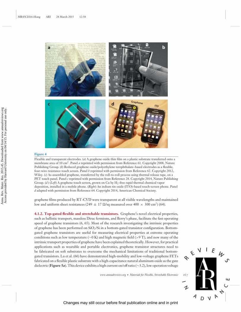
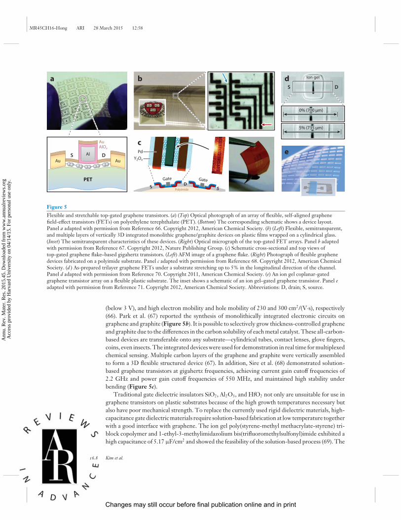
4.1.2. Top-gated flexible and stretchable transistors. Graphene’s novel electrical properties,such as ballistic transport, massless Dirac fermions, and Berry’s phase, facilitate the fast operatingspeed of graphene transistors (6, 65). Most of the research investigating the intrinsic propertiesof graphene has been performed on SiO2/Si in a bottom-gated transistor configuration. Bottom-gated graphene transistors are useful for measuring electrical properties at extreme operatingconditions such as low temperature (∼0 K) and high magnetic field (>9 T), and now many of theintrinsic transport properties of graphene have been explained theoretically. However, for practicalapplications such as wearable and portable electronics, graphene transistor structures need tobe fabricated on soft substrates to overcome the mechanical limitations of traditional bottom-gated transistors. Lu et al. (66) have demonstrated high-mobility and low-voltage graphene FETsfabricated on a flexible plastic substrate with a high-capacitance natural aluminum oxide as the gatedielectric (Figure 5a). This device exhibits a high current on/off ratio (∼3.2), low operation voltage
www.annualreviews.org • Materials for Flexible, Stretchable Electronics 16.7
Changes may still occur before final publication online and in print
Ann
u. R
ev. M
ater
. Res
. 201
5.45
. Dow
nloa
ded
from
ww
w.a
nnua
lrev
iew
s.or
g A
cces
s pr
ovid
ed b
y H
arva
rd U
nive
rsity
on
04/1
4/15
. For
per
sona
l use
onl
y.
MR45CH16-Hong ARI 28 March 2015 12:58
a b d
ce
AlOx
Y2Ox
Pd
Au
Al
Au Au
Polyimide
DS
PET
Ion gelIon gel
DS
0% (700 μm)0% (700 μm)
5% (735 μm)5% (735 μm)
Gate
SD
S
Gate
Figure 5Flexible and stretchable top-gated graphene transistors. (a) (Top) Optical photograph of an array of flexible, self-aligned graphenefield-effect transistors (FETs) on polyethylene terephthalate (PET). (Bottom) The corresponding schematic shows a device layout.Panel a adapted with permission from Reference 66. Copyright 2012, American Chemical Society. (b) (Left) Flexible, semitransparent,and multiple layers of vertically 3D integrated monolithic graphene/graphite devices on plastic films wrapped on a cylindrical glass.(Inset) The semitransparent characteristics of these devices. (Right) Optical micrograph of the top-gated FET arrays. Panel b adaptedwith permission from Reference 67. Copyright 2012, Nature Publishing Group. (c) Schematic cross-sectional and top views oftop-gated graphene flake–based gigahertz transistors. (Left) AFM image of a graphene flake. (Right) Photograph of flexible graphenedevices fabricated on a polyimide substrate. Panel c adapted with permission from Reference 68. Copyright 2012, American ChemicalSociety. (d ) As-prepared trilayer graphene FETs under a substrate stretching up to 5% in the longitudinal direction of the channel.Panel d adapted with permission from Reference 70. Copyright 2011, American Chemical Society. (e) An ion gel coplanar-gatedgraphene transistor array on a flexible plastic substrate. The inset shows a schematic of an ion gel–gated graphene transistor. Panel eadapted with permission from Reference 71. Copyright 2012, American Chemical Society. Abbreviations: D, drain; S, source.
(below 3 V), and high electron mobility and hole mobility of 230 and 300 cm2/(V·s), respectively(66). Park et al. (67) reported the synthesis of monolithically integrated electronic circuits ongraphene and graphite (Figure 5b). It is possible to selectively grow thickness-controlled grapheneand graphite due to the differences in the carbon solubility of each metal catalyst. These all-carbon-based devices are transferable onto any substrate—cylindrical tubes, contact lenses, glove fingers,coins, even insects. The integrated devices were used for demonstration in real time for multiplexedchemical sensing. Multiple carbon layers of the graphene and graphite were vertically assembledto form a 3D flexible structured device (67). In addition, Sire et al. (68) demonstrated solution-based graphene transistors at gigahertz frequencies, achieving current gain cutoff frequencies of2.2 GHz and power gain cutoff frequencies of 550 MHz, and maintained high stability underbending (Figure 5c).
Traditional gate dielectric insulators SiO2, Al2O3, and HfO2 not only are unsuitable for use ingraphene transistors on plastic substrates because of the high growth temperatures necessary butalso have poor mechanical strength. To replace the currently used rigid dielectric materials, high-capacitance gate dielectric materials require solution-based fabrication at low temperature togetherwith a good interface with graphene. The ion gel poly(styrene-methyl methacrylate-styrene) tri-block copolymer and 1-ethyl-3-methylimidazolium bis(trifluoromethylsulfonyl)imide exhibited ahigh capacitance of 5.17 μF/cm2 and showed the feasibility of the solution-based process (69). The
16.8 Kim et al.
Changes may still occur before final publication online and in print
Ann
u. R
ev. M
ater
. Res
. 201
5.45
. Dow
nloa
ded
from
ww
w.a
nnua
lrev
iew
s.or
g A
cces
s pr
ovid
ed b
y H
arva
rd U
nive
rsity
on
04/1
4/15
. For
per
sona
l use
onl
y.
MR45CH16-Hong ARI 28 March 2015 12:58
ion gel–gated graphene transistors provided both high on/off current and low-voltage operation.Lee et al. (70) presented a stretchable and transparent all-graphene transistor array on a stretchablerubber substrate by using an ion gel dielectric in a low-temperature printing process (Figure 5d ).Such monolithic graphene devices had hole and electron mobilities of 1,188 ± 136 and 422 ±52 cm2/(V·s), respectively, with stable operation of more than 1,000 stretching cycles (70). Kimet al. (71) reported transparent, flexible graphene transistors and inverters in a coplanar-gate con-figuration made by a printing process; such devices consisted of only two materials: graphene andan ion gel gate dielectric (Figure 5e). These devices exhibited excellent performance, includinglow-voltage operation with a high transistor on current and mobility, excellent mechanical flexi-bility, environmental stability, and reasonable inverting behavior upon connecting two transistors(71).
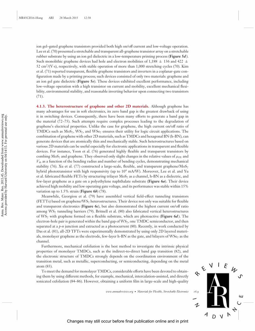
4.1.3. The heterostructure of graphene and other 2D materials. Although graphene hasmany advantages for use in soft electronics, its zero band gap is the greatest drawback of usingit in switching devices. Consequently, there have been many efforts to generate a band gap inthe material (72–75). Such attempts require complex processes leading to the degradation ofgraphene’s electrical properties. Unlike the case for graphene, the high current on/off ratio ofTMDCs such as MoS2, WS2, and WSe2 ensures their utility for logic circuit applications. Thecombination of graphene with other 2D materials, such as TMDCs and hexagonal BN (h-BN), cangenerate devices that are atomically thin and mechanically stable. Such heterostructures based onvarious 2D materials can be useful especially for electronic applications in transparent and flexibledevices. For instance, Yoon et al. (76) generated highly flexible and transparent transistors bycombing MoS2 and graphene. They observed only slight changes in the relative values of μFE andVth as a function of the bending radius and number of bending cycles, demonstrating mechanicalstability (76). Xu et al. (77) constructed a large-scale, flexible, and transparent graphene/MoS2
hybrid phototransistor with high responsivity (up to 104 mA/W). Moreover, Lee et al. and Yuet al. fabricated flexible FETs by structuring trilayer MoS2 as a channel, h-BN as a dielectric, andfew-layer graphene as a gate on a polyethylene naphthalate substrate (Figure 6a). Their deviceachieved high mobility and low operating gate voltage, and its performance was stable within 15%variation up to 1.5% strain (Figure 6b) (78).
Meanwhile, Georgiou et al. (79) have assembled vertical field-effect tunneling transistors(FETTs) based on graphene/WS2 heterostructures. Their device not only was suitable for flexibleand transparent electronics (Figure 6c), but also demonstrated the highest current on/off ratioamong WS2 tunneling barriers (79). Britnell et al. (80) also fabricated vertical heterostructuresof WS2 with graphene formed on a flexible substrate, which are photoactive (Figure 6d ). Theelectron-hole pair is generated within the band gap of WS2, one TMDC semiconductor, and thenseparated at a p-n junction and extracted as a photocurrent (80). Recently, in work conducted byDas et al. (81), all-2D TFTs were experimentally demonstrated by using only 2D layered materi-als, monolayer graphene as the electrode, few-layer h-BN as the gate, and bilayers of WSe2 as thechannel.
Furthermore, mechanical exfoliation is the best method to investigate the intrinsic physicalproperties of monolayer TMDCs, such as the indirect-to-direct band gap transition (82), andthe electronic structure of TMDCs strongly depends on the coordination environment of thetransition metal, such as metallic, superconducting, or semiconducting, depending on the metalatom (83).
To meet the demand for monolayer TMDCs, considerable efforts have been devoted to obtain-ing them by using different methods, for example, mechanical, intercalation-assisted, and directlysonicated exfoliation (84–86). However, obtaining a uniform film in large-scale and high-quality
www.annualreviews.org • Materials for Flexible, Stretchable Electronics 16.9
Changes may still occur before final publication online and in print
Ann
u. R
ev. M
ater
. Res
. 201
5.45
. Dow
nloa
ded
from
ww
w.a
nnua
lrev
iew
s.or
g A
cces
s pr
ovid
ed b
y H
arva
rd U
nive
rsity
on
04/1
4/15
. For
per
sona
l use
onl
y.
MR45CH16-Hong ARI 28 March 2015 12:58
h-BN
MoS2
GraGraGraGrGraGrGGGGrapphephehhephephephpheephpppppppppppp neeneee
a
3 μm
b
0.0
0.8
1.0
1.2
1.4
1.6
1.8
0.5 1.0
Strain (%)
µ/µ 0
1.5
c d1 cm
Strain of 1.5%
Figure 6Flexible and heterostructure devices. (a) An optical micrograph of device consists of MoS2, h-BN, and graphene (MBG). Each dashedline indicates the border of each of these materials. (b) Relative field-effect mobility of the MBG device as a function of strain. Theinsets show a schematic diagram of the MBG device and a photograph of the device. The arrows indicate the y-direction for strain.Panels a and b adapted with permission from Reference 78. Copyright 2013, American Chemical Society. (c) A photograph of a flexibleand transparent transistor composed of WS2, h-BN, and graphene. Panel c adapted with permission from Reference 79. Copyright2013, Nature Publishing Group. (d ) A photograph of a flexible device composed of WS2 between graphene electrodes. Panel d adaptedwith permission from Reference 80. Copyright 2013, American Association for the Advancement of Science.
TMDCs has been challenging. To overcome these problems, the CVD method was recently de-veloped to synthesize a scalable TMDC thin layer directly on various insulator substrates such asSiO2, sapphire, and SrTiO3. In the sulfurization approach, redeposited Mo metal or Mo oxidelayers were reacted with a S precursor from solid- or gas-phase sources (87). This approach, us-ing Mo metal, has been used to synthesize large-area and uniform MoS2 films on SiO2 with anon/off ratio of ∼105 but with a relatively low mobility of 0.07 cm2/(V·s)—which is attributable tothe presence of small grains—and, consequently, many grain boundaries (88). In addition, large-area and highly crystalline MoS2 was produced by the thermolysis of ammonium thiomolybdate[(NH4)2MoS4] with a S precursor at high temperatures (89). Although sulfurization is an effectivemethod to grow large-area thin films, synthesizing large-area monolayers of TMDCs is difficult. Inanother approach, gaseous metal and chalcogenide precursors are simultaneously introduced intothe chamber. This method is usually employed to synthesize larger grain size, higher crystallinity,and improved electrical properties compared with sulfurization using Mo or W compounds (90–92). Therefore, the latter is the only suitable method to grow uniform monolayers with large areaand grain size.
4.2. Graphene-Based Organic and Inorganic LEDs
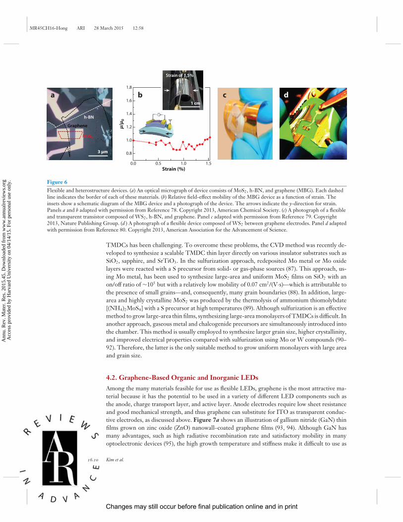
Among the many materials feasible for use as flexible LEDs, graphene is the most attractive ma-terial because it has the potential to be used in a variety of different LED components such asthe anode, charge transport layer, and active layer. Anode electrodes require low sheet resistanceand good mechanical strength, and thus graphene can substitute for ITO as transparent conduc-tive electrodes, as discussed above. Figure 7a shows an illustration of gallium nitride (GaN) thinfilms grown on zinc oxide (ZnO) nanowall–coated graphene films (93, 94). Although GaN hasmany advantages, such as high radiative recombination rate and satisfactory mobility in manyoptoelectronic devices (95), the high growth temperature and stiffness make it difficult to use as
16.10 Kim et al.
Changes may still occur before final publication online and in print
Ann
u. R
ev. M
ater
. Res
. 201
5.45
. Dow
nloa
ded
from
ww
w.a
nnua
lrev
iew
s.or
g A
cces
s pr
ovid
ed b
y H
arva
rd U
nive
rsity
on
04/1
4/15
. For
per
sona
l use
onl
y.
MR45CH16-Hong ARI 28 March 2015 12:58
a b
c d e
13 V
17 V15 V
11 V
13 mm 10 mm 7 mm
R = ∞ R = 5.5 mm R = 3.9 mm
GraHILGraHIL
5.95 eV5.95 eV
NPBNPB
5.4 eV5.4 eV
4.4 eV4.4 eV
hh
hh
hh
hh
Al
Al
4.3 eV
5.2 eV
2.7 eV
4.95 eV
4.79 eV
3.64 eV
4.7 eV
ITO
LiF
Super yellow
GO
ITO
4.89 eV
1.29 eV
Su
pe
r y
ell
owG
O
rGO
OO
OOO–O–
HOHO
O–O–
O–O–
O–O–
OHOH
OHOH
OHOH
OO
OO
OO
OO
OO
Figure 7Graphene-based flexible light-emitting diodes (LEDs). (a) An illustration of a ZnO nanostructure directly grown on a graphene-based,transferable, GaN thin-film LED. Panel a reprinted with permission from Reference 94. Copyright 2011, Nature Publishing Group.(b) Light emission of heteroepitaxial growth of GaN/ZnO coaxial nanorod heterostructures on large-area graphene film at bendingradii of ∞, 5.5, and 3.9 mm. Panel b adapted with permission from Reference 96. Copyright 2011, Wiley. (c) A schematic illustration ofa hole injection process from a graphene anode through a self-organized gradient hole injection layer (graHIL), which provides a workfunction gradient to the NPB [N,N′-bis(naphthalene-1-yl)-N,N′-bis(phenyl) benzidine] layer. Panel c adapted with permission fromReference 102. Copyright 2011, Nature Publishing Group. (d ) (Left) A schematic of a device architecture of polymer LEDs (PLEDs)using graphene oxide (GO) as a hole transport layer. (Right) Comparison of energy diagrams of flat-band conditions of PLEDs withregard to GO, reduced graphene oxide (rGO), and poly(3,4-ethylene dioxythiophene) polystyrene sulfonate. Panel d adapted withpermission from Reference 107. Copyright 2012, American Chemical Society. (e) A uniform and bluish-white light emission from thefabricated LED utilizing ZnO/graphene quasi-quantum dots with applied biases of 11, 13, 15, and 17 V. Panel e adapted withpermission from Reference 109. Copyright 2012, Nature Publishing Group.
components in flexible optoelectronics. The poor electrical properties of sapphire as a substratealso limit possible device performance. Separation of GaN from the growth substrate circum-vents these obstacles, allowing for the growth of GaN thin film on ZnO-coated graphene thatexhibits high-temperature compatibility and yet is transferable onto arbitrary substrates. For flex-ible devices, Lee et al. (96) demonstrated GaN/ZnO coaxial nanorod heterostructures grown ongraphene and transferred nanostructure LEDs onto Cu-coated PET, which tolerated bendingradii of 5.5 and 3.9 mm (Figure 7b). Furthermore, graphene not only facilitates coverage andself-organization of the overlying organic materials, but also meets electrical property require-ments such as work function and sheet resistance by the doping process (45, 97). It has provedpossible to produce highly efficient OLEDs by using a composition of doped multilayer graphene
www.annualreviews.org • Materials for Flexible, Stretchable Electronics 16.11
Changes may still occur before final publication online and in print
Ann
u. R
ev. M
ater
. Res
. 201
5.45
. Dow
nloa
ded
from
ww
w.a
nnua
lrev
iew
s.or
g A
cces
s pr
ovid
ed b
y H
arva
rd U
nive
rsity
on
04/1
4/15
. For
per
sona
l use
onl
y.

MR45CH16-Hong ARI 28 March 2015 12:58
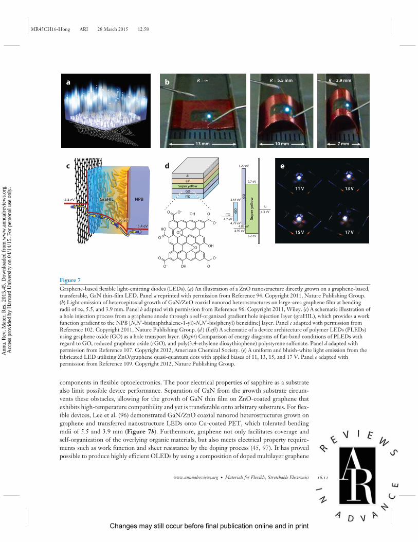
and conducting polymer composition (98–101), contributing to low operating voltages and toan easier hole injection from the graphene electrode to organic layers [N,N′-bis(naphthalene-1-yl)-N,N′-bis(phenyl) benzidine] (Figure 7c). Han et al. (102) reported that OLEDs with modi-fied graphene approach higher luminous efficiencies (37.2 lm/W in fluorescence) than with ITO(24.1 lm/W in fluorescence). Technical enhancements in the electrical properties of graphenealso allowed for the fabrication of a flexible white OLED lighting device on PET. Matyba et al.(99) recently reported flexible and metal-free light-emitting electrochemical cells based on chem-ically derived graphene as a cathode and poly(3,4-ethylene dioxythiophene) polystyrene sulfonate(PEDOS:PSS) as an anode. These devices exhibited a low turn-on voltage for yellow light emission(V = 2.8 V) and good efficiency (2.4 cd/A) (87). Also, Hyun et al. (103) demonstrated foldablegraphene circuits. These circuits were successfully prepared on paper by vacuum filtration andselective transfer from the membrane filter to paper to create LED chips.
Unlike CVD-grown graphene, which exhibits a short hot-carrier lifetime and zero band gap,chemically exfoliated graphene such as GO and graphene quantum dots have emerged as a holetransport layer, presumably because they exhibit a certain band gap due to the quantum con-finement or edge effect (104–106). Lee et al. (107) investigated polymer light-emitting diodes(PLEDs) with a solution-based GO interlayer as a hole transport layer (Figure 7d ). GO filmswith wide band gap maximize hole-electron recombination within the active layer. As a result,PLEDs with a GO film show a 220% increase in luminous efficiency and a 280% enhancementin power conversion efficiency (107). Recently, there have also been many efforts to synthesizehybrid nanocomposites consisting of graphene/nanomaterial heterostructures as candidates forfabricating a novel class of optoelectronics (108–110). Son et al. (109) demonstrated, by a sim-ple solution process, white LED-based hybrid quantum dots consisting of a ZnO core wrappedin a shell of graphene quantum dots with a brightness of 798 cd/m2 (Figure 7e). Furthermore,GO-wrapped poly(9,9-di-n-octylfluorenyl-2,7-diyl) nanoparticles exhibit unique white-emittingphotoluminescence with a characteristic green-emissive broadband above 500 nm (98). Hence,GO, graphene quantum dots, and hybrid nanostructures utilized as a carrier transport layer andas an active layer are important for flexible optoelectronics.
4.3. Graphene-Based Energy Storage and Conversion
In many flexible devices, the development of energy storage and harvesting units is as important asthe flexibility of the displays. However, most current conventional energy devices are heavy, rigid,and bulky and so are not compatible with the use of flexible electronics. To meet the needs ofthe next generation of energy devices, considerable effort is being devoted to making the currentdevices light, small, flexible, and shape conforming while maintaining the outstanding mechanicalproperties of Li-ion batteries (LIBs), supercapacitors, solar cells, and nanogenerators.
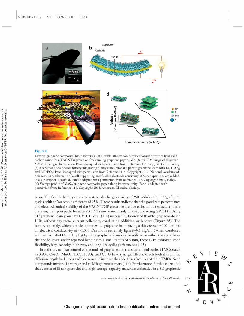
4.3.1. Lithium-ion batteries. Making flexible/stretchable energy devices requires the develop-ment of soft, electrode-active materials such as metal oxide nanoparticles or nanoparticle coatingsas cathodes and Li film or advanced-carbon materials as anodes. Among various carbon materials,graphene has been studied as a potential electrode material for LIBs due to its excellent electricalproperties, theoretically large specific surface area (2,630 m2/g), and high Young’s modulus(∼1 TPa). Soft LIBs have provoked great interest due to their high energy density, long run cycle,and excellent rate capability for flexible/stretchable electronics (111–113). Li et al. (114) reportedthat vertically aligned CNTs (VACNTs) directly grown onto freestanding graphene paper (GP)showed outstanding conductivity and high mechanical strength (Figure 8a). Even after 10,000bending cycles, the structure and electrical properties of VACNT/GP were stable over a long
16.12 Kim et al.
Changes may still occur before final publication online and in print
Ann
u. R
ev. M
ater
. Res
. 201
5.45
. Dow
nloa
ded
from
ww
w.a
nnua
lrev
iew
s.or
g A
cces
s pr
ovid
ed b
y H
arva
rd U
nive
rsity
on
04/1
4/15
. For
per
sona
l use
onl
y.
MR45CH16-Hong ARI 28 March 2015 12:58
a b
cc d
VACNTsVACNTs
GP
Cathode
Separator
Anode
e–
e–
Specific capacity (mAh/g)
Vo
lta
ge
(|V
| v
ers
us
Na
/Na
+)
NaC
Mo
S
Figure 8Flexible graphene composite–based batteries. (a) Flexible lithium-ion batteries consist of vertically alignedcarbon nanotubes (VACNTs) grown on freestanding graphene paper (GP). (Inset) SEM image of as-grownVACNTs on graphene paper. Panel a adapted with permission from Reference 114. Copyright 2011, Wiley.(b) A schematic of a flexible battery integrating highly conductive and porous graphene foam with Li4Ti5O12and LiFePO4. Panel b adapted with permission from Reference 115. Copyright 2012, National Academy ofSciences. (c) A schematic of a self-supporting and flexible electrode consisting of Si nanoparticles embeddedin a 3D graphenic scaffold. Panel c adapted with permission from Reference 117. Copyright 2011, Wiley.(d ) Voltage profile of MoS2/graphene composite paper along its crystallinity. Panel d adapted withpermission from Reference 118. Copyright 2014, American Chemical Society.
term. The flexible battery exhibited a stable discharge capacity of 290 mAh/g at 30 mA/g after 40cycles, with a Coulombic efficiency of 95%. These results indicate that the good rate performanceand electrochemical stability of the VACNT/GP electrode are due to its unique structure; thereare many transport paths because VACNTs are rooted firmly on the conducting GP (114). Using3D graphene foam grown by CVD, Li et al. (114) successfully fabricated flexible, graphene-basedLIBs without any metal current collectors, conducting additives, or binders (Figure 8b). Thebattery assembly, which is made up of flexible graphene foam having a thickness of ∼100 μm, hasan electrical conductivity of ∼1,000 S/m and is extremely light (∼0.1 mg/cm2) when combinedwith either LiFePO4 or Li4Ti5O12. The graphene foam can be utilized as either the cathode orthe anode. Even under repeated bending to a small radius of 5 mm, these LIBs exhibited goodflexibility, high capacity, high rate, and long-life cyclic performance (115).
In addition, nanostructured compounds of graphene and transition metal oxides (TMOs) suchas SnO2, Co3O4, MnO2, TiO2, Fe3O4, and Cu2O have synergic effects, which both shorten thediffusion length for Li ions and electrons and increase the specific surface area of these TMOs. Suchcompounds increase Li storage and yield high conductivity (116). Furthermore, flexible electrodesthat consist of Si nanoparticles and high-storage-capacity materials embedded in a 3D graphenic
www.annualreviews.org • Materials for Flexible, Stretchable Electronics 16.13
Changes may still occur before final publication online and in print
Ann
u. R
ev. M
ater
. Res
. 201
5.45
. Dow
nloa
ded
from
ww
w.a
nnua
lrev
iew
s.or
g A
cces
s pr
ovid
ed b
y H
arva
rd U
nive
rsity
on
04/1
4/15
. For
per
sona
l use
onl
y.
MR45CH16-Hong ARI 28 March 2015 12:58
scaffold achieved an exceptional reversible capacity of ∼1,100 mAh/g at 8 A/g or approximately3,200 mAh/g at 1 A/g, repeatable up to 99.9% between cycles for more than 150 cycles (Figure 8c)(117). Freestanding paper composed of graphene and TMDCs was introduced into flexible LIBs aswell as into Na-ion batteries, resulting in improved capacity and high efficiency (Figure 8d ) (118).
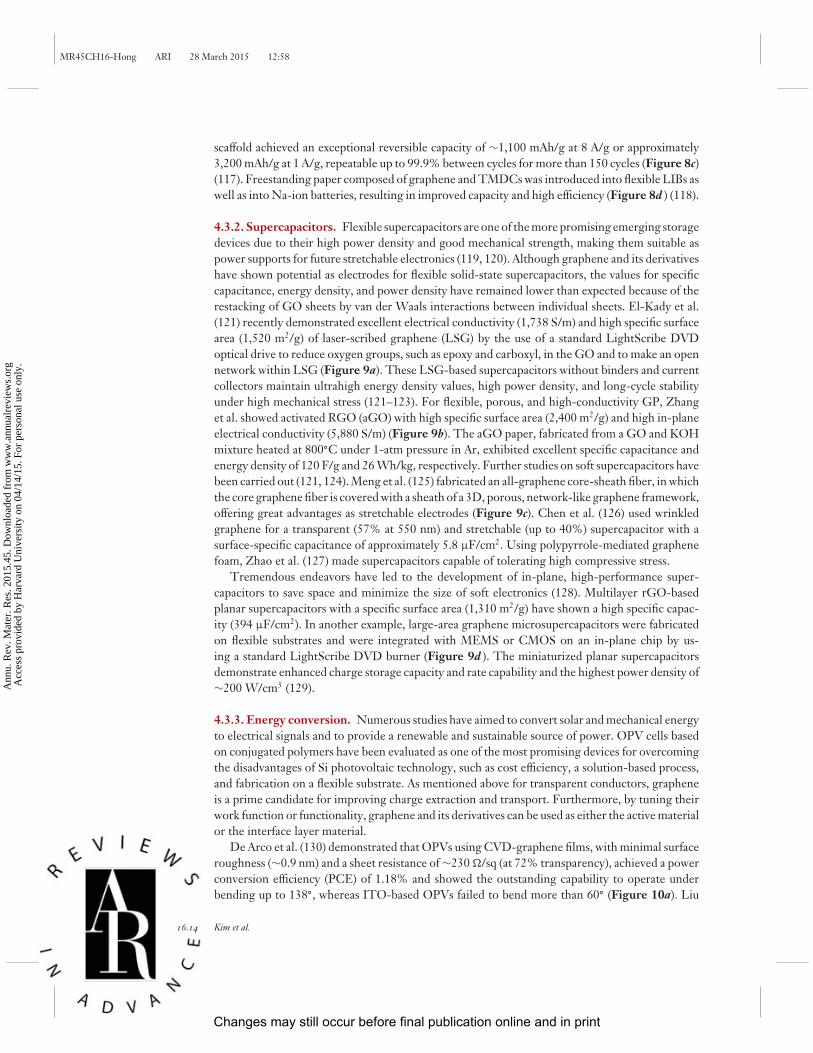
4.3.2. Supercapacitors. Flexible supercapacitors are one of the more promising emerging storagedevices due to their high power density and good mechanical strength, making them suitable aspower supports for future stretchable electronics (119, 120). Although graphene and its derivativeshave shown potential as electrodes for flexible solid-state supercapacitors, the values for specificcapacitance, energy density, and power density have remained lower than expected because of therestacking of GO sheets by van der Waals interactions between individual sheets. El-Kady et al.(121) recently demonstrated excellent electrical conductivity (1,738 S/m) and high specific surfacearea (1,520 m2/g) of laser-scribed graphene (LSG) by the use of a standard LightScribe DVDoptical drive to reduce oxygen groups, such as epoxy and carboxyl, in the GO and to make an opennetwork within LSG (Figure 9a). These LSG-based supercapacitors without binders and currentcollectors maintain ultrahigh energy density values, high power density, and long-cycle stabilityunder high mechanical stress (121–123). For flexible, porous, and high-conductivity GP, Zhanget al. showed activated RGO (aGO) with high specific surface area (2,400 m2/g) and high in-planeelectrical conductivity (5,880 S/m) (Figure 9b). The aGO paper, fabricated from a GO and KOHmixture heated at 800◦C under 1-atm pressure in Ar, exhibited excellent specific capacitance andenergy density of 120 F/g and 26 Wh/kg, respectively. Further studies on soft supercapacitors havebeen carried out (121, 124). Meng et al. (125) fabricated an all-graphene core-sheath fiber, in whichthe core graphene fiber is covered with a sheath of a 3D, porous, network-like graphene framework,offering great advantages as stretchable electrodes (Figure 9c). Chen et al. (126) used wrinkledgraphene for a transparent (57% at 550 nm) and stretchable (up to 40%) supercapacitor with asurface-specific capacitance of approximately 5.8 μF/cm2. Using polypyrrole-mediated graphenefoam, Zhao et al. (127) made supercapacitors capable of tolerating high compressive stress.
Tremendous endeavors have led to the development of in-plane, high-performance super-capacitors to save space and minimize the size of soft electronics (128). Multilayer rGO-basedplanar supercapacitors with a specific surface area (1,310 m2/g) have shown a high specific capac-ity (394 μF/cm2). In another example, large-area graphene microsupercapacitors were fabricatedon flexible substrates and were integrated with MEMS or CMOS on an in-plane chip by us-ing a standard LightScribe DVD burner (Figure 9d ). The miniaturized planar supercapacitorsdemonstrate enhanced charge storage capacity and rate capability and the highest power density of∼200 W/cm3 (129).
4.3.3. Energy conversion. Numerous studies have aimed to convert solar and mechanical energyto electrical signals and to provide a renewable and sustainable source of power. OPV cells basedon conjugated polymers have been evaluated as one of the most promising devices for overcomingthe disadvantages of Si photovoltaic technology, such as cost efficiency, a solution-based process,and fabrication on a flexible substrate. As mentioned above for transparent conductors, grapheneis a prime candidate for improving charge extraction and transport. Furthermore, by tuning theirwork function or functionality, graphene and its derivatives can be used as either the active materialor the interface layer material.
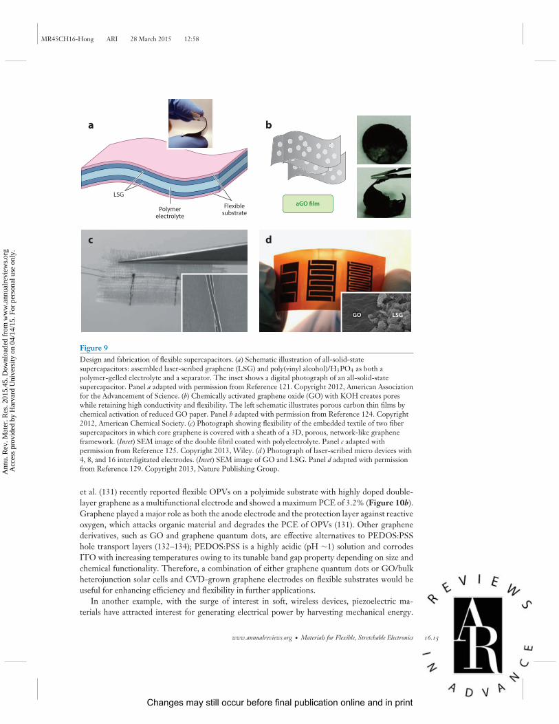
De Arco et al. (130) demonstrated that OPVs using CVD-graphene films, with minimal surfaceroughness (∼0.9 nm) and a sheet resistance of ∼230 �/sq (at 72% transparency), achieved a powerconversion efficiency (PCE) of 1.18% and showed the outstanding capability to operate underbending up to 138◦, whereas ITO-based OPVs failed to bend more than 60◦ (Figure 10a). Liu
16.14 Kim et al.
Changes may still occur before final publication online and in print
Ann
u. R
ev. M
ater
. Res
. 201
5.45
. Dow
nloa
ded
from
ww
w.a
nnua
lrev
iew
s.or
g A
cces
s pr
ovid
ed b
y H
arva
rd U
nive
rsity
on
04/1
4/15
. For
per
sona
l use
onl
y.
MR45CH16-Hong ARI 28 March 2015 12:58
a b
c d
GOGO LSGLSG
aGO film
LSG
Flexiblesubstrate
Polymerelectrolyte
Figure 9Design and fabrication of flexible supercapacitors. (a) Schematic illustration of all-solid-statesupercapacitors: assembled laser-scribed graphene (LSG) and poly(vinyl alcohol)/H3PO4 as both apolymer-gelled electrolyte and a separator. The inset shows a digital photograph of an all-solid-statesupercapacitor. Panel a adapted with permission from Reference 121. Copyright 2012, American Associationfor the Advancement of Science. (b) Chemically activated graphene oxide (GO) with KOH creates poreswhile retaining high conductivity and flexibility. The left schematic illustrates porous carbon thin films bychemical activation of reduced GO paper. Panel b adapted with permission from Reference 124. Copyright2012, American Chemical Society. (c) Photograph showing flexibility of the embedded textile of two fibersupercapacitors in which core graphene is covered with a sheath of a 3D, porous, network-like grapheneframework. (Inset) SEM image of the double fibril coated with polyelectrolyte. Panel c adapted withpermission from Reference 125. Copyright 2013, Wiley. (d ) Photograph of laser-scribed micro devices with4, 8, and 16 interdigitated electrodes. (Inset) SEM image of GO and LSG. Panel d adapted with permissionfrom Reference 129. Copyright 2013, Nature Publishing Group.
et al. (131) recently reported flexible OPVs on a polyimide substrate with highly doped double-layer graphene as a multifunctional electrode and showed a maximum PCE of 3.2% (Figure 10b).Graphene played a major role as both the anode electrode and the protection layer against reactiveoxygen, which attacks organic material and degrades the PCE of OPVs (131). Other graphenederivatives, such as GO and graphene quantum dots, are effective alternatives to PEDOS:PSShole transport layers (132–134); PEDOS:PSS is a highly acidic (pH ∼1) solution and corrodesITO with increasing temperatures owing to its tunable band gap property depending on size andchemical functionality. Therefore, a combination of either graphene quantum dots or GO/bulkheterojunction solar cells and CVD-grown graphene electrodes on flexible substrates would beuseful for enhancing efficiency and flexibility in further applications.
In another example, with the surge of interest in soft, wireless devices, piezoelectric ma-terials have attracted interest for generating electrical power by harvesting mechanical energy.
www.annualreviews.org • Materials for Flexible, Stretchable Electronics 16.15
Changes may still occur before final publication online and in print
Ann
u. R
ev. M
ater
. Res
. 201
5.45
. Dow
nloa
ded
from
ww
w.a
nnua
lrev
iew
s.or
g A
cces
s pr
ovid
ed b
y H
arva
rd U
nive
rsity
on
04/1
4/15
. For
per
sona
l use
onl
y.
MR45CH16-Hong ARI 28 March 2015 12:58
0.0
Graphene
Dark
2θ = 0
2θ = 83
2θ = 138
Voltage (V)
Cu
rre
nt
de
nsi
ty
(mA
/cm
2)
0.4 0.8–0.4–4
–2
0
2
4
0.0
ITOPMMA/graphenePMMA/graphene
PEDOT:PSS (Au)
P3HT:PCBM
ZnO
AuPl
Metal
Voltage (V)
p-NC
Au/Cr
p-NC
Plastic substra
te
0.4 0.8–0.4
–4
–6
–2
0
2
4
6
Light Light
Dark
2θ = 0
2θ = 36
2θ = 60
a b
c dLi2CoO2
PVDF
Graphene
Cu film
Kapton
Al film
Figure 10Flexible and stretchable energy conversion devices. (a) Current-voltage characteristics of CVD-grown graphene (left) and indium tinoxide (ITO) (right) solar cells under bending and 100 mW/cm2 AM1.5G spectral illumination. Insets show the experimental setupemployed in the experiments. Panel a adapted with permission from Reference 130. Copyright 2010, American Chemical Society.(b) The inverted structure of a flexible organic photovoltaic cell with a graphene top electrode on a polyimide substrate. Panel b adaptedwith permission from Reference 131. Copyright 2013, Wiley. (c) The design of a flexible, self-charging power cell using graphenenanosheet–coated Cu foil as an anode, polarized polyvinylidene fluoride (PVDF) film as a separator, and LiCoO2-coated Al foil as acathode. Abbreviations: PEDOT:PSS, poly(3,4-ethylene dioxythiophene) polystyrene sulfonate; PMMA, polymethyl methacrylate.Panel c adapted with permission from Reference 136. Copyright 2014, Wiley. (d ) A photograph of a stretchable piezoelectricnanocomposite (p-NC) (a mixture of BaTiO3 and graphitic carbon). (Inset) The structure of the p-NC/Au/Cr/plastic substrate. Panel dadapted with permission from Reference 139. Copyright 2012, Wiley.
Nanogenerators have been used in flexible, stretchable devices, in body-implanted devices, andin biosensors, converting biomechanical energy into electricity inside the human body. Choiet al. (135) recently reported fully rollable and transparent piezoelectric energy-harvesting nano-generators, heterogeneous 3D nanostructures consisting of 1D ZnO nanorods on 2D graphene,using CVD-grown graphene as transparent electrodes and ZnO nanorods as the platform forgrowth. Xue et al. (136) demonstrated flexible, self-charging power cells in liquid electrolyte.These power cells consisted of layers of kapton film, flexible graphene, and polyvinylidenefluoride as the piezoelectric (Figure 10c). Such flexible devices can be effectively charged by themovement of the human body or machines (136). In addition, graphene-based lead zirconatetitanate nanogenerators also exhibited good mechanical bendability, good semitransparency,and high performance (137). Park et al. (138, 139) found nanocomposite generators based onpiezoelectric BaTiO3 nanoparticles and graphitic carbon materials such as CNTs or RGO asthe stress-reinforcing agent and conducting functional material (Figure 10d ). Their devicewas achieved through a simple, low-cost, and large-area fabrication process that generated anelectrical signal by bending or by movements of human fingers (138, 139).
16.16 Kim et al.
Changes may still occur before final publication online and in print
Ann
u. R
ev. M
ater
. Res
. 201
5.45
. Dow
nloa
ded
from
ww
w.a
nnua
lrev
iew
s.or
g A
cces
s pr
ovid
ed b
y H
arva
rd U
nive
rsity
on
04/1
4/15
. For
per
sona
l use
onl
y.
MR45CH16-Hong ARI 28 March 2015 12:58
5. SUMMARY
We review recent representative developments of devices incorporating graphene with organic,inorganic, or other 2D materials (including transparent electrodes, transistors, LEDs, OPVs,LIBs, and supercapacitors) for flexible and stretchable applications. Graphene films obtained bydifferent chemical or mechanical methods can be transferred onto various polymer substrates andused as transparent electrodes, as conducting channels in transistors, and as active layers in devices.In addition, hybrid structures of graphene combined with other 2D materials have dimensionaladvantages that are more appropriate for flexible and stretchable electronics. Developing newstrategies to obtain high-quality graphene and engineering the characteristics of graphene wouldprovide promising device platforms for a wide variety of applications.
DISCLOSURE STATEMENT
The authors are not aware of any affiliations, memberships, funding, or financial holdings thatmight be perceived as affecting the objectivity of this review.
ACKNOWLEDGMENTS
This work was supported by the Global Research Lab Program (2011-0021972), the GlobalFrontier Research Program (2011-0031629), and the Basic Science Research Program (2011-0017587) through the National Research Foundation of Korea funded by the Korean government[Ministry of Education, Science, and Technology (MEST) and Ministry of Knowledge Economy(MKE)].
LITERATURE CITED
1. Ahn J-H, Hong BH. 2014. Graphene for displays that bend. Nat. Nanotechnol. 9:737–382. Novoselov KS, Geim AK, Morozov SV, Jiang D, Zhang Y, et al. 2004. Electric field effect in atomically
thin carbon films. Science 306:666–693. Novoselov KS, McCann E, Morozov SV, Fal’ko VI, Katsnelson MI, et al. 2006. Unconventional quantum
Hall effect and Berry’s phase of 2π in bilayer graphene. Nat. Phys. 2:177–804. Jiang Z, Zhang Y, Tan YW, Stormer HL, Kim P. 2007. Quantum Hall effect in graphene. Solid State
Commun. 143:14–195. Jiang Z, Zhang Y, Stormer HL, Kim P. 2007. Quantum Hall states near the charge-neutral Dirac point
in graphene. Phys. Rev. Lett. 99:1068026. Zhang Y, Tan Y-W, Stormer HL, Kim P. 2005. Experimental observation of the quantum Hall effect
and Berry’s phase in graphene. Nature 438:201–47. Novoselov KS, Jiang Z, Zhang Y, Morozov SV, Stormer HL, et al. 2007. Room-temperature quantum
Hall effect in graphene. Science 315:13798. Geim AK, Novoselov KS. 2007. The rise of graphene. Nat. Mater. 6:183–919. Katsnelson MI. 2007. Graphene: carbon in two dimensions. Mater. Today 10:20–27
10. Stankovich S, Dikin DA, Dommett GHB, Kohlhaas KM, Zimney EJ, et al. 2006. Graphene-basedcomposite materials. Nature 442:282–86
11. Stankovich S, Dikin DA, Piner RD, Kohlhaas KA, Kleinhammes A, et al. 2007. Synthesis of graphene-based nanosheets via chemical reduction of exfoliated graphite oxide. Carbon 45:1558–65
12. Jung I, Dikin DA, Piner RD, Ruoff RS. 2008. Tunable electrical conductivity of individual grapheneoxide sheets reduced at “low” temperatures. Nano Lett. 8:4283–87
13. Yang D, Velamakanni A, Bozoklu G, Park S, Stoller M, et al. 2009. Chemical analysis of graphene oxidefilms after heat and chemical treatments by X-ray photoelectron and micro-Raman spectroscopy. Carbon47:145–52
www.annualreviews.org • Materials for Flexible, Stretchable Electronics 16.17
Changes may still occur before final publication online and in print
Ann
u. R
ev. M
ater
. Res
. 201
5.45
. Dow
nloa
ded
from
ww
w.a
nnua
lrev
iew
s.or
g A
cces
s pr
ovid
ed b
y H
arva
rd U
nive
rsity
on
04/1
4/15
. For
per
sona
l use
onl
y.
MR45CH16-Hong ARI 28 March 2015 12:58
14. Berger C, Song Z, Li X, Wu X, Brown N, et al. 2006. Electronic confinement and coherence in patternedepitaxial graphene. Science 312:1191–96
15. de Heer WA, Berger C, Wu X, First PN, Conrad EH, et al. 2007. Epitaxial graphene. Solid State Commun.143:92–100
16. Hass J, de Heer WA, Conrad EH. 2008. The growth and morphology of epitaxial multilayer graphene.J. Phys. Condens. Matter 20:323202
17. Lin Y-M, Dimitrakopoulos C, Jenkins KA, Farmer DB, Chiu H-Y, et al. 2010. 100-GHz transistorsfrom wafer-scale epitaxial graphene. Science 327:662
18. Sun Z, Yan Z, Yao J, Beitler E, Zhu Y, Tour JM. 2010. Growth of graphene from solid carbon sources.Nature 468:549–52
19. Byun S-J, Lim H, Shin G-Y, Han T-H, Oh SH, et al. 2011. Graphenes converted from polymers. Phys.Chem. Lett. 2:493–97
20. Li X, Cai W, An J, Kim S, Nah J, et al. 2009. Large-area synthesis of high-quality and uniform graphenefilms on copper foils. Science 324:1312–14
21. Kwon S-Y, Ciobanu CV, Petrova V, Shenoy VB, Bareno J, et al. 2009. Growth of semiconductinggraphene on palladium. Nano Lett. 9:3985–90
22. Sutter PW, Flege J-I, Sutter EA. 2008. Epitaxial graphene on ruthenium. Nat. Mater. 7:406–1123. Coraux J, N’Diaye AT, Busse C, Michely T. 2008. Structural coherency of graphene on Ir(111). Nano
Lett. 8:565–7024. Kim KS, Zhao Y, Jang H, Lee SY, Kim JM, et al. 2009. Large-scale pattern growth of graphene films
for stretchable transparent electrodes. Nature 457:706–1025. Shin H-A-S, Ryu J, Cho S-P, Lee E-K, Cho S, et al. 2014. Highly uniform growth of monolayer graphene
by chemical vapor deposition on Cu-Ag alloy catalysts. Phys. Chem. Chem. Phys. 16:3087–9426. Dai B, Fu L, Zou Z, Wang M, Xu H, et al. 2011. Rational design of a binary metal alloy for chemical
vapour deposition growth of uniform single-layer graphene. Nat. Commun. 2:52227. Chen S, Brown L, Levendorf M, Cai W, Ju S-Y, et al. 2011. Oxidation resistance of graphene-coated
Cu and Cu/Ni alloy. ACS Nano 5:1321–2728. Bae S, Kim H, Lee Y, Xu X, Park J-S, et al. 2010. Roll-to-roll production of 30-inch graphene films for
transparent electrodes. Nat. Nanotechnol. 5:574–7829. Kobayashi T, Bando M, Kimura N, Shimizu K, Kadono K, et al. 2013. Production of a 100-m-long
high-quality graphene transparent conductive film by roll-to-roll chemical vapor deposition and transferprocess. Appl. Phys. Lett. 102:023112
30. Malesevic A, Vitchev R, Schouteden K, Volodin A, Zhang L, et al. 2008. Synthesis of few-layer graphenevia microwave plasma-enhanced chemical vapour deposition. Nanotechnology 19:305604
31. Malesevic A, Kemps R, Vanhulsel A, Chowdhury MP, Volodin A, Van Haesendonck C. 2008. Fieldemission from vertically aligned few-layer graphene. J. Appl. Phys. 104:084301
32. Shang NG, Papakonstantinou P, McMullan M, Chu M, Stamboulis A, et al. 2008. Catalyst-free efficientgrowth, orientation and biosensing properties of multilayer graphene nanoflake films with sharp edgeplanes. Adv. Funct. Mater. 18:3506–14
33. Kim Y-J, Kim SJ, Jung MH, Choi KY, Bae S, et al. 2012. Low-temperature growth and direct transferof graphene-graphitic carbon films on flexible plastic substrates. Nanotechnology 23:344016
34. Lee Y, Bae S, Jang H, Jang S, Zhu S-E, et al. 2010. Wafer-scale synthesis and transfer of graphene films.Nano Lett. 10:490–93
35. Kang J, Hwang S, Kim JH, Kim MH, Ryu J, et al. 2012. Efficient transfer of large-area graphene filmsonto rigid substrates by hot pressing. ACS Nano 6:5360–65
36. Gunes F, Shin H-J, Biswas C, Han GH, Kim ES, et al. 2010. Layer-by-layer doping of few-layer graphenefilm. ACS Nano 4:4595–600
37. Kasry A, Kuroda MA, Martyna GJ, Tulevski GS, Bol AA. 2010. Chemical doping of large-area stackedgraphene films for use as transparent, conducting electrodes. ACS Nano 4:3839–44
38. Li X, Zhu Y, Cai W, Borysiak M, Han B, et al. 2009. Transfer of large-area graphene films for high-performance transparent conductive electrodes. Nano Lett. 9:4359–63
39. Ismach A, Druzgalski C, Penwell S, Schwartzberg A, Zheng M, et al. 2010. Direct chemical vapordeposition of graphene on dielectric surfaces. Nano Lett. 10:1542–48
16.18 Kim et al.
Changes may still occur before final publication online and in print
Ann
u. R
ev. M
ater
. Res
. 201
5.45
. Dow
nloa
ded
from
ww
w.a
nnua
lrev
iew
s.or
g A
cces
s pr
ovid
ed b
y H
arva
rd U
nive
rsity
on
04/1
4/15
. For
per
sona
l use
onl
y.
MR45CH16-Hong ARI 28 March 2015 12:58
40. Bi H, Sun S, Huang F, Xie X, Jiang M. 2012. Direct growth of few-layer graphene films on SiO2
substrates and their photovoltaic applications. J. Mater. Chem. 22:411–1641. Kim H, Song I, Park C, Son M, Hong M, et al. 2013. Copper-vapor-assisted chemical vapor deposition
for high-quality and metal-free single-layer graphene on amorphous SiO2 substrate. ACS Nano 7:6575–82
42. Bolotin KI, Sikes KJ, Jiang Z, Klima M, Fudenberg G, et al. 2008. Ultrahigh electron mobility insuspended graphene. Solid State Commun. 146:351–55
43. Lee C, Wei X, Kysar JW, Hone J. 2008. Measurement of the elastic properties and intrinsic strength ofmonolayer graphene. Science 321:385–88
44. Nair RR, Blake P, Grigorenko AN, Novoselov KS, Booth TJ, et al. 2008. Fine structure constant definesvisual transparency of graphene. Science 320:1308
45. Park J, Lee WH, Huh S, Sim SH, Kim SB, et al. 2011. Work-function engineering of graphene electrodesby self-assembled monolayers for high-performance organic field-effect transistors. J. Phys. Chem. Lett.2:841–45
46. Park J, Jo SB, Yu Y-J, Kim Y, Yang JW, et al. 2012. Single-gate bandgap opening of bilayer grapheneby dual molecular doping. Adv. Mater. 24:407–11
47. Wu J, Xie L, Li Y, Wang H, Ouyang Y, et al. 2011. Controlled chlorine plasma reaction for noninvasivegraphene doping. J. Am. Chem. Soc. 133:19668–71
48. Guo B, Liu Q, Chen E, Zhu H, Fang L, Gong JR. 2010. Controllable N-doping of graphene. Nano Lett.10:4975–80
49. Wei D, Liu Y, Wang Y, Zhang H, Huang L, Yu G. 2009. Synthesis of N-doped graphene by chemicalvapor deposition and its electrical properties. Nano Lett. 9:1752–58
50. Chen W, Chen S, Qi DC, Gao XY, Wee ATS. 2007. Surface transfer p-type doping of epitaxial graphene.J. Am. Chem. Soc. 129:10418–22
51. Medina H, Lin Y-C, Obergfell D, Chiu P-W. 2011. Tuning of charge densities in graphene by moleculedoping. Adv. Funct. Mater. 21:2687–92
52. Kim SJ, Ryu J, Son S, Yoo JM, Park JB, et al. 2014. Simultaneous etching and doping by Cu-stabilizingagent for high-performance graphene-based transparent electrodes. Chem. Mater. 26:2332–36
53. Bonaccorso F, Sun Z, Hasan T, Ferrari AC. 2010. Graphene photonics and optoelectronics. NaturePhotonics 4:611–22
54. Ellmer K. 2012. Past achievements and future challenges in the development of optically transparentelectrodes. Nature Photonics 6:809–17
55. Hecht DS, Hu L, Irvin G. 2011. Emerging transparent electrodes based on thin films of carbon nanotubes,graphene, and metallic nanostructures. Adv. Mater. 23:1482–513
56. Sierros KA, Morris NJ, Kukureka SN, Cairns DR. 2009. Dry and wet sliding wear of ITO-coated PETcomponents used in flexible optoelectronic applications. Wear 267:625–31
57. Cairns DR, Witte RP, Sparacin DK, Sachsman SM, Paine DC, et al. 2000. Strain-dependent electricalresistance of tin-doped indium oxide on polymer substrates. Appl. Phys. Lett. 76:1425–27
58. Becerril HA, Mao J, Liu Z, Stoltenberg RM, Bao Z, Chen Y. 2008. Evaluation of solution-processedreduced graphene oxide films as transparent conductors. ACS Nano 2:463–70
59. He Q, Wu S, Gao S, Cao X, Yin Z, et al. 2011. Transparent, flexible, all-reduced graphene oxide thinfilm transistors. ACS Nano 5:5038–44
60. Wu S, Yin Z, He Q, Huang X, Zhou X, Zhang H. 2010. Electrochemical deposition of semiconductoroxides on reduced graphene oxide–based flexible, transparent, and conductive electrodes. J. Phys. Chem.C 114:11816–21
61. Eda G, Fanchini G, Chhowalla M. 2008. Large-area ultrathin films of reduced graphene oxide as atransparent and flexible electronic material. Nat. Nanotechnol. 3:270–74
62. Wang J, Liang M, Fang Y, Qiu T, Zhang J, Zhi L. 2012. Rod-coating: towards large-area fabrication ofuniform reduced graphene oxide films for flexible touch screens. Adv. Mater. 24:2874–78
63. Zhou Y, Bao Q, Tang LAL, Zhong Y, Loh KP. 2009. Hydrothermal dehydration for the “green” reduc-tion of exfoliated graphene oxide to graphene and demonstration of tunable optical limiting properties.Chem. Mater. 21:2950–56
www.annualreviews.org • Materials for Flexible, Stretchable Electronics 16.19
Changes may still occur before final publication online and in print
Ann
u. R
ev. M
ater
. Res
. 201
5.45
. Dow
nloa
ded
from
ww
w.a
nnua
lrev
iew
s.or
g A
cces
s pr
ovid
ed b
y H
arva
rd U
nive
rsity
on
04/1
4/15
. For
per
sona
l use
onl
y.
MR45CH16-Hong ARI 28 March 2015 12:58
64. Ryu J, Kim Y, Won D, Kim N, Park JS, et al. 2013. Fast synthesis of high-performance graphene filmsby hydrogen-free rapid thermal chemical vapor deposition. ACS Nano 8:950–56
65. Novoselov KS, Geim AK, Morozov SV, Jiang D, Katsnelson MI, et al. 2005. Two-dimensional gas ofmassless Dirac fermions in graphene. Nature 438:197–200
66. Lu C-C, Lin Y-C, Yeh C-H, Huang J-C, Chiu P-W. 2012. High mobility flexible graphene field-effecttransistors with self-healing gate dielectrics. ACS Nano 6:4469–74
67. Park J-U, Nam S, Lee M-S, Lieber CM. 2012. Synthesis of monolithic graphene–graphite integratedelectronics. Nat. Mater. 11:120–25
68. Sire C, Ardiaca F, Lepilliet S, Seo J-WT, Hersam MC, et al. 2012. Flexible gigahertz transistors derivedfrom solution-based single-layer graphene. Nano Lett. 12:1184–88
69. Kim BJ, Jang H, Lee S-K, Hong BH, Ahn J-H, Cho JH. 2010. High-performance flexible graphene fieldeffect transistors with ion gel gate dielectrics. Nano Lett. 10:3464–66
70. Lee S-K, Kim BJ, Jang H, Yoon SC, Lee C, et al. 2011. Stretchable graphene transistors with printeddielectrics and gate electrodes. Nano Lett. 11:4642–46
71. Kim BJ, Lee S-K, Kang MS, Ahn J-H, Cho JH. 2012. Coplanar-gate transparent graphene transistorsand inverters on plastic. ACS Nano 6:8646–51
72. Han MY, Ozyilmaz B, Zhang Y, Kim P. 2007. Energy band-gap engineering of graphene nanoribbons.Phys. Rev. Lett. 98:206805
73. Ni ZH, Yu T, Lu YH, Wang YY, Feng YP, Shen ZX. 2008. Uniaxial strain on graphene: Ramanspectroscopy study and band-gap opening. ACS Nano 2:2301–5
74. Zhang Y, Tang T-T, Girit C, Hao Z, Martin MC, et al. 2009. Direct observation of a widely tunablebandgap in bilayer graphene. Nature 459:820–23
75. Zhou SY, Gweon GH, Fedorov AV, First PN, de Heer WA, et al. 2007. Substrate-induced bandgapopening in epitaxial graphene. Nat. Mater. 6:770–75
76. Yoon J, Park W, Bae G-Y, Kim Y, Jang HS, et al. 2013. Highly flexible and transparent multilayer MoS2
transistors with graphene electrodes. Small 9:3295–30077. Xu H, Wu J, Feng Q, Mao N, Wang C, Zhang J. 2014. High responsivity and gate tunable graphene-
MoS2 hybrid phototransistor. Small 10:2300–678. Lee G-H, Yu Y-J, Cui X, Petrone N, Lee C-H, et al. 2013. Flexible and transparent MoS2 field-effect
transistors on hexagonal boron nitride–graphene heterostructures. ACS Nano 7:7931–3679. Georgiou T, Jalil R, Belle BD, Britnell L, Gorbachev RV, et al. 2013. Vertical field-effect transistor based
on graphene-WS2 heterostructures for flexible and transparent electronics. Nat. Nanotechnol. 8:100–380. Britnell L, Ribeiro RM, Eckmann A, Jalil R, Belle BD, et al. 2013. Strong light-matter interactions in
heterostructures of atomically thin films. Science 340:1311–1481. Das S, Gulotty R, Sumant AV, Roelofs A. 2014. All two-dimensional, flexible, transparent, and thinnest
thin film transistor. Nano Lett. 14:2861–6682. Splendiani A, Sun L, Zhang Y, Li T, Kim J, et al. 2010. Emerging photoluminescence in monolayer
MoS2. Nano Lett. 10:1271–7583. Wilson JA, Yoffe AD. 1969. The transition metal dichalcogenides discussion and interpretation of the
observed optical, electrical and structural properties. Adv. Phys. 18:193–33584. Radisavljevic B, Radenovic A, Brivio J, Giacometti V, Kis A. 2011. Single-layer MoS2 transistors. Nat
Nanotechnol. 6:147–5085. Zeng Z, Yin Z, Huang X, Li H, He Q, et al. 2011. Single-layer semiconducting nanosheets: high-yield
preparation and device fabrication. Angew. Chem. Int. Ed. 50:11093–9786. Coleman JN, Lotya M, O’Neill A, Bergin SD, King PJ, et al. 2011. Two-dimensional nanosheets pro-
duced by liquid exfoliation of layered materials. Science 331:568–7187. Wang X, Feng H, Wu Y, Jiao L. 2013. Controlled synthesis of highly crystalline MoS2 flakes by chemical
vapor deposition. J. Am. Chem. Soc. 135:5304–788. Lee Y, Lee J, Bark H, Oh I-K, Ryu GH, et al. 2014. Synthesis of wafer-scale uniform molybdenum
disulfide films with control over the layer number using a gas phase sulfur precursor. Nanoscale 6:2821–26
89. Liu K-K, Zhang W, Lee Y-H, Lin Y-C, Chang M-T, et al. 2012. Growth of large-area and highlycrystalline MoS2 thin layers on insulating substrates. Nano Lett. 12:1538–44
16.20 Kim et al.
Changes may still occur before final publication online and in print
Ann
u. R
ev. M
ater
. Res
. 201
5.45
. Dow
nloa
ded
from
ww
w.a
nnua
lrev
iew
s.or
g A
cces
s pr
ovid
ed b
y H
arva
rd U
nive
rsity
on
04/1
4/15
. For
per
sona
l use
onl
y.

MR45CH16-Hong ARI 28 March 2015 12:58
90. Zhang J, Yu H, Chen W, Tian X, Liu D, et al. 2014. Scalable growth of high-quality polycrystallineMoS2 monolayers on SiO2 with tunable grain sizes. ACS Nano 8:6024–30
91. Song I, Park C, Hong M, Baik J, Shin H-J, Choi HC. 2014. Patternable large-scale molybdenium disulfideatomic layers grown by gold-assisted chemical vapor deposition. Angew. Chem. Int. Ed. 53:1266–69
92. Duan X, Wang C, Shaw JC, Cheng R, Chen Y, et al. 2014. Lateral epitaxial growth of two-dimensionallayered semiconductor heterojunctions. Nat. Nanotechnol. 9:1024–30
93. Chung K, Lee C-H, Yi G-C. 2010. Transferable GaN layers grown on ZnO-coated graphene layers foroptoelectronic devices. Science 330:655–57
94. 2011. Semiconductors: LEDs lift off. NPG Asia Mater. doi: 10.1038/asiamat.2011.1095. Ponce FA, Bour DP. 1997. Nitride-based semiconductors for blue and green light-emitting devices.
Nature 386:351–5996. Lee C-H, Kim Y-J, Hong YJ, Jeon S-R, Bae S, et al. 2011. Flexible inorganic nanostructure light-emitting
diodes fabricated on graphene films. Adv. Mater. 23:4614–1997. Jeong YJ, Jang J, Nam S, Kim K, Kim LH, et al. 2014. High-performance organic complementary
inverters using monolayer graphene electrodes. ACS Appl. Mater. Interfaces 6:6816–2498. Ha J, Park S, Kim D, Ryu J, Lee C, et al. 2013. High-performance polymer light emitting diodes with
interface-engineered graphene anodes. Org. Electron. 14:2324–3099. Matyba P, Yamaguchi H, Eda G, Chhowalla M, Edman L, Robinson ND. 2010. Graphene and mobile
ions: the key to all-plastic, solution-processed light-emitting devices. ACS Nano 4:637–42100. Kim D, Lee D, Lee Y, Jeon DY. 2013. Work-function engineering of graphene anode by
bis(trifluoromethanesulfonyl)amide doping for efficient polymer light-emitting diodes. Adv. Funct.Mater. 23:5049–55
101. Chang H, Wang G, Yang A, Tao X, Liu X, et al. 2010. A transparent, flexible, low-temperature, andsolution-processible graphene composite electrode. Adv. Funct. Mater. 20:2893–902
102. Han T-H, Lee Y, Choi M-R, Woo S-H, Bae S-H, et al. 2012. Extremely efficient flexible organiclight-emitting diodes with modified graphene anode. Nature Photonics 6:105–10
103. Hyun WJ, Park OO, Chin BD. 2013. Foldable graphene electronic circuits based on paper substrates.Adv. Mater. 25:4729–34
104. Mei Q, Zhang K, Guan G, Liu B, Wang S, Zhang Z. 2010. Highly efficient photoluminescent grapheneoxide with tunable surface properties. Chem. Commun. 46:7319–21
105. Loh KP, Bao Q, Eda G, Chhowalla M. 2010. Graphene oxide as a chemically tunable platform for opticalapplications. Nat. Chem. 2:1015–24
106. Tetsuka H, Asahi R, Nagoya A, Okamoto K, Tajima I, et al. 2012. Optically tunable amino-functionalizedgraphene quantum dots. Adv. Mater. 24:5333–38
107. Lee BR, Kim J-W, Kang D, Lee DW, Ko S-J, et al. 2012. Highly efficient polymer light-emitting diodesusing graphene oxide as a hole transport layer. ACS Nano 6:2984–91
108. Kwon W, Kim Y-H, Lee C-L, Lee M, Choi HC, et al. 2014. Electroluminescence from graphenequantum dots prepared by amidative cutting of tattered graphite. Nano Lett. 14:1306–11
109. Son DI, Kwon BW, Park DH, Seo W-S, Yi Y, et al. 2012. Emissive ZnO-graphene quantum dots forwhite-light-emitting diodes. Nat. Nanotechnol. 7:465–71
110. Yoo DY, Tu NDK, Lee SJ, Lee E, Jeon S-R, et al. 2014. Graphene oxide nanosheet wrapped white-emissive conjugated polymer nanoparticles. ACS Nano 8:4248–56
111. Armand M, Tarascon JM. 2008. Building better batteries. Nature 451:652–57112. Gwon H, Kim H-S, Lee KU, Seo D-H, Park YC, et al. 2011. Flexible energy storage devices based on
graphene paper. Energy Environ. Sci. 4:1277–83113. Lee S-Y, Choi K-H, Choi W-S, Kwon YH, Jung H-R, et al. 2013. Progress in flexible energy storage
and conversion systems, with a focus on cable-type lithium-ion batteries. Energy Environ. Sci. 6:2414–23114. Li S, Luo Y, Lv W, Yu W, Wu S, et al. 2011. Vertically aligned carbon nanotubes grown on graphene
paper as electrodes in lithium-ion batteries and dye-sensitized solar cells. Adv. Energy Mater. 1:486–90115. Li N, Chen Z, Ren W, Li F, Cheng H-M. 2012. Flexible graphene-based lithium ion batteries with
ultrafast charge and discharge rates. PNAS 109:17360–65116. Huang X, Qi X, Boey F, Zhang H. 2012. Graphene-based composites. Chem. Soc. Rev. 41:666–86
www.annualreviews.org • Materials for Flexible, Stretchable Electronics 16.21
Changes may still occur before final publication online and in print
Ann
u. R
ev. M
ater
. Res
. 201
5.45
. Dow
nloa
ded
from
ww
w.a
nnua
lrev
iew
s.or
g A
cces
s pr
ovid
ed b
y H
arva
rd U
nive
rsity
on
04/1
4/15
. For
per
sona
l use
onl
y.
MR45CH16-Hong ARI 28 March 2015 12:58
117. Zhao X, Hayner CM, Kung MC, Kung HH. 2011. In-plane vacancy-enabled high-power Si–graphenecomposite electrode for lithium-ion batteries. Adv. Energy Mater. 1:1079–84
118. David L, Bhandavat R, Singh G. 2014. MoS2/graphene composite paper for sodium-ion battery elec-trodes. ACS Nano 8:1759–70
119. Zhang LL, Zhao XS. 2009. Carbon-based materials as supercapacitor electrodes. Chem. Soc. Rev. 38:2520–31
120. Lu Q, Chen JG, Xiao JQ. 2013. Nanostructured electrodes for high-performance pseudocapacitors.Angew. Chem. Int. Ed. 52:1882–89
121. El-Kady MF, Strong V, Dubin S, Kaner RB. 2012. Laser scribing of high-performance and flexiblegraphene-based electrochemical capacitors. Science 335:1326–30
122. Zhu Y, Murali S, Stoller MD, Ganesh KJ, Cai W, et al. 2011. Carbon-based supercapacitors producedby activation of graphene. Science 332:1537–41
123. Strong V, Dubin S, El-Kady MF, Lech A, Wang Y, et al. 2012. Patterning and electronic tuning of laserscribed graphene for flexible all-carbon devices. ACS Nano 6:1395–403
124. Zhang LL, Zhao X, Stoller MD, Zhu Y, Ji H, et al. 2012. Highly conductive and porous activated reducedgraphene oxide films for high-power supercapacitors. Nano Lett. 12:1806–12
125. Meng Y, Zhao Y, Hu C, Cheng H, Hu Y, et al. 2013. All-graphene core-sheath microfibers for all-solid-state, stretchable fibriform supercapacitors and wearable electronic textiles. Adv. Mater. 25:2326–31
126. Chen T, Xue Y, Roy AK, Dai L. 2014. Transparent and stretchable high-performance supercapacitorsbased on wrinkled graphene electrodes. ACS Nano 8:1039–46
127. Zhao Y, Liu J, Hu Y, Cheng H, Hu C, et al. 2013. Highly compression-tolerant supercapacitor basedon polypyrrole-mediated graphene foam electrodes. Adv. Mater. 25:591–95
128. Yoo JJ, Balakrishnan K, Huang J, Meunier V, Sumpter BG, et al. 2011. Ultrathin planar graphenesupercapacitors. Nano Lett. 11:1423–27
129. El-Kady MF, Kaner RB. 2013. Scalable fabrication of high-power graphene micro-supercapacitors forflexible and on-chip energy storage. Nat. Commun. 4:1475
130. Gomez De Arco L, Zhang Y, Schlenker CW, Ryu K, Thompson ME, Zhou C. 2010. Continuous, highlyflexible, and transparent graphene films by chemical vapor deposition for organic photovoltaics. ACSNano 4:2865–73
131. Liu Z, Li J, Yan F. 2013. Package-free flexible organic solar cells with graphene top electrodes. Adv.Mater. 25:4296–301
132. Li S-S, Tu K-H, Lin C-C, Chen C-W, Chhowalla M. 2010. Solution-processable graphene oxide as anefficient hole transport layer in polymer solar cells. ACS Nano 4:3169–74
133. Park H, Brown PR, Bulovic V, Kong J. 2011. Graphene as transparent conducting electrodes in organicphotovoltaics: studies in graphene morphology, hole transporting layers, and counter electrodes. NanoLett. 12:133–40
134. Kim JK, Park MJ, Kim SJ, Wang DH, Cho SP, et al. 2013. Balancing light absorptivity and carrierconductivity of graphene quantum dots for high-efficiency bulk heterojunction solar cells. ACS Nano7:7207–12
135. Choi D, Choi M-Y, Choi WM, Shin H-J, Park H-K, et al. 2010. Fully rollable transparent nanogeneratorsbased on graphene electrodes. Adv. Mater. 22:2187–92
136. Xue X, Deng P, He B, Nie Y, Xing L, et al. 2014. Flexible self-charging power cell for one-step energyconversion and storage. Adv. Energy Mater. 4:1301329
137. Kwon J, Seung W, Sharma BK, Kim S-W, Ahn J-H. 2012. A high performance PZT ribbon-basednanogenerator using graphene transparent electrodes. Energy Environ. Sci. 5:8970–75
138. Park K-I, Xu S, Liu Y, Hwang G-T, Kang S-JL, et al. 2010. Piezoelectric BaTiO3 thin film nanogeneratoron plastic substrates. Nano Lett. 10:4939–43
139. Park K-I, Lee M, Liu Y, Moon S, Hwang G-T, et al. 2012. Flexible nanocomposite generator made ofBaTiO3 nanoparticles and graphitic carbons. Adv. Mater. 24:2999–3004
16.22 Kim et al.
Changes may still occur before final publication online and in print
Ann
u. R
ev. M
ater
. Res
. 201
5.45
. Dow
nloa
ded
from
ww
w.a
nnua
lrev
iew
s.or
g A
cces
s pr
ovid
ed b
y H
arva
rd U
nive
rsity
on
04/1
4/15
. For
per
sona
l use
onl
y.