Embed Size (px)
Citation preview
GRAPHENE-BASED
UV-CURED MATERIALS
Marco Sangermano
Politecnico di Torino, Dipartimento di Scienza Applicata e Tecnologia, C.so Duca degli Abruzzi 24, 10129, Torino.
1. INTRODUCTION Nowadays we are witnessing an increasing request for electronic devices production characterized by high demanding properties such as low manufacturing cost, long-time endurance, environmental sustainable production methods, recycling, low energy consumption and high efficiency. Polymeric materials seem to be the most promising candidates to meet all these challenges1. In this paper we report two different approach in which graphene-based UV-cured materials were proposed for the possible fabrication of devices. The first one is the study of formulation of graphene-based UV-curable inks, to get printed circuits boards, the second is related to the achievement of flexible transparent graphene-based capacitor. Inkjet printing is one of the most promising manufacturing technique which can be used to deposit polymers on a variety of substrates2. In the inkjet printing, low viscosity should be maintained in the polymer precursor and fast polymerization needs to be performed soon after the deposition. For these reasons, the use of UV curing process seems to be very interesting because it undergoes at room temperature, allowing the ink polymerization even on thermal sensitive substrates such as paper, and in addition is a fast overall manufacturing process3. In order to decrease the surface resistivity of the dielectric polymer network, it is necessary to disperse conductive fillers in the precursor, to reach a conductive network. Carbon-based materials can be good candidates for conductive inks, due to their low cost and good electrical conductivity without the need of temperature treatments. This has been demonstrated for carbon nanotubes printed thin films4, graphene bi- and tri-layer used as protective coating against oxidation on copper NPs-based inks5, and in graphene/water suspensions6. Because of its high specific surface area, good chemical stability, electrical and thermal conductivity and high charge carrier mobility (20 m2 V−1 s−1)7,8, graphene is actually the most suitable candidate to be dispersed in photo-curable formulations in order to obtain a UV-cured conductive ink. This work explores the possibility of introducing aqueous dispersion of GO into acrylic resin matrices, such as poly(ethylene glycol) diacrylate (PEGDA), thus fabricating a conductive printable
ink which is environmentally friendly9. The reduction of GO was performed using UV light irradiation, which allowed the simultaneous photo-polymerization of the polymeric matrix10, which acted as a binder. Structural and electrical characterization showed the efficiency of the reduction method and promising values of conductivity of printed test patterns. Quite recently, graphene has also become the focus of a considerable amount of research as (super)capacitor electrode11. As a matter of fact, graphene is considered as one of the most suitable substrate material for preparing electrodes. In this field graphene-conducting polymer composites are becoming the most suitable choice to prepare flexible capacitors. Zhao and coworkers12 fabricated graphene-PANI composites through an in-situ polymerization of aniline monomer in the presence of graphene oxide under acidic conditions. The preparation of the nanocomposite was then followed by the reduction of graphene oxide to graphene using hydrazine. Chen and coworkers13 prepared graphene-PANI composites as a flexible electrode, combining the advantages of graphene such as high conductivity, mechanical strength and flexibility and the PANI conducting polymer characterized by large capacity. Lee and coworkers14 established a nanoarchitecture involving polypyrrole and graphene nanosheets through in-situ polymerization. In our research we have followed a new strategy to prepare graphene based polymer electrode. A graphene to SU8 epoxy polymer transfer method was established15. After the graphene transfer to polymer, the SU8 film presents two distinct surfaces: a conductive surface obtained by the homogeneous and continuous graphene layer, and an electrically insulating one, typical for the dielectric epoxy material. Two SU8 films were bonded together with an UV-curable cycloaliphatic epoxy resin, in order to have two parallel graphene-conductive layers separated by epoxy dielectric materials acting as an adhesive in between the two SU8 sheets. 2. EXPERIMENTAL 2.1 Materials Commercial reagents were used: GO (thickness 0.7 - 1.2 nm) was purchased from Cheap Tubes Inc. (USA) and used without further purification, PEGDA with Mw=575 g mol-2 was purchased from Sigma-Aldrich and DAROCUR® 1173 radical photoinitiator (PI) from BASF. PEGDA was chosen as polymeric matrix due to its non-toxicity and water solubility, in order to fabricate an environmentally friendly ink. The SU8 (SU8-3010, Micro-Chem®, density 1.106 g/ml) epoxy based photoresist was adopted to act both as the dielectric and as the supporting layer for the graphene membranes. The epoxy resin (3,4-Epoxycyclohexylmethyl-3,4-epoxycyclohexane carboxylate, resin CE, Sigma-Aldrich®, molecular weight 252.31 g/mol) was selected as the UV-curable epoxy resin. Triphenylsulfonium hexafluoroantimonate (Aldrich, as 50% solution in propylene carbonate, PI), was added as cationic photoinitiator. 2.2 Samples preparation 2.2.1 GO aqueous dispersion/PEGDA UV-curable inks (GOp) The formulations were prepared adding 0.5 g of PEGDA and 0.08 g of PI to 4.5 g of DI water in which 0.02 g of GO was previously dispersed (samples referred to as GOp, and corresponding to the GO/PI ratio of 1/4). This GO/PEGDA/water ink was tested by inkjet spotting straight line patterns with variable resolution (85 to 190 dots-per-inch, dpi) and repetition of passes on the same track (from 1 to 5) on microscope slides.
The printed thin films were irradiated with UV light for two minutes. As a reference for bulk nanocomposite material, 100 µm thick films of the GOp were obtained by deposition on a microscope slide glass using a wire-wound bar and subsequently exposed to UV light for two minutes. As a reference for electrical characterization, a PEGDA/PI thick film was similarly prepared without adding GO. 2.2.2 Graphene based capacitor preparation Graphene membranes have been synthesized by means of Chemical Vapour Deposition (CVD) at 1000°C using copper as a catalyst and methane as the carbon feedstock. The processes produced continuous graphene films composed by 1 - 3 layers [15], with similar sheet resistance values, in the range 0.5 – 1 kΩ/□, and transmittances, at 550 nm, of about 92. A 10 µm thick layer of negative tone resist SU8-3010 has been deposited by means of spin-coating on as-grown graphene membranes, without any adhesion promoter. After a preliminary soft bake at 95°C , the Cu substrates/graphene/SU8 sandwiches have been exposed to UV-light illumination and then a two-step baking process, at 65°C and 95°C respectively, has been performed. To further crosslink the SU8 polymer, a hard bake at 200°C was finally done. Thereafter, G/SU8 membranes have been released from the grown substrates by means of a room temperature wet etching of the Cu layers. A FeCl3/HCl solution has been used to etch the evaporated Cu thin film, whereas a HNO3: H2O (1:3) solution was adopted for the Cu foil removal. Finally, after a thorough rinsing in De-Ionized (DI) H2O, the free-standing G/SU8 membranes have been gathered and dried overnight.Typically, two SU8 films with graphene transferred onto one side, were bonded using the CE resin as adhesive. The non-conductive SU8 side of a G/SU8 membrane was coated with the epoxy resin (containing 2 wt% of cationic photoinitiator) by using a wirewound applicator in order to get a film thickness of about 25 µm. The two SU8 sides of the membranes were then bonded by leaving the conductive side containing graphene on the outer surface. The sandwich film was irradiated for 2 minutes, realizing a capacitor stacked structure (graphene/SU8/epoxy/SU8/graphene) and then subjected to electrical characterization. 2.3 Characterization The structural analysis and morphology of thick and thin printed films were characterized by optical and scanning electron microscopy (SEM). X-ray photoelectron spectroscopy (XPS) was performed using a monochromatic X-ray beam with an Al K-α source with energy of 1486.6 eV. Before performing XPS, the homogeneity of the samples was verified using an in-situ secondary X-ray imaging. Current/voltage (I-V) measurements were performed on thick and printed films using a standard two-point micro-contact setup of a Keithley 2635A multimeter. The electrical characterization was performed on all samples at room temperature, in the range -200 to +200 V. Resistivity was computed comparing GO/PEGDA thick films with printed thin films of several thicknesses (varied with dpi resolution and repetition of printing on the same track, measured by profilometry). These measurements were planned in order to assess the variation in resistivity due to GO reduction to graphene by UV irradiation, and any potential collateral effects produced by the high strain rate to which inks are submitted to in the printing nozzle.
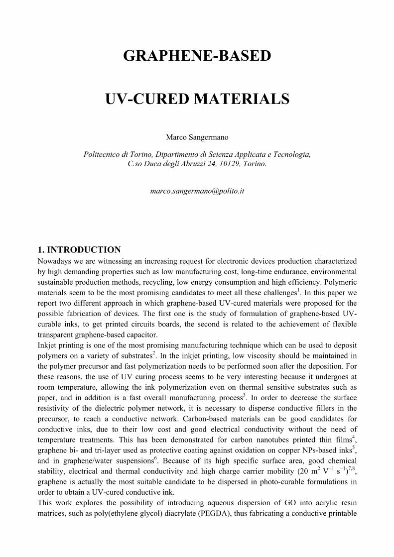
Impedance spectroscopy was also performed on the devices, by means of an Agilent E4980A precision LCR meter at room temperature, in the range 20 Hz – 2 MHz, with a signal amplitude ranging from 100 mV up to 10V, using the same contact setup as described above. 3. RESULTS AND DISCUSSION 3.1 UV-curable inks We have investigated conductive printable inks, based on acrylic-aqueous UV-curable formulations containing GO. The oxide can be easily dispersed in water and it can be reduced during UV irradiation, with the simultaneous build up of the acrylic crosslinking network. The polymer network acts as a binder during printing and the in-situ reduced GO decreases the resistivity of the acrylic polymer, forming a conductive percolative network. This method can be used for the preparation of aqueous acrylic formulations of variable viscosity, which are suitable for the fabrication of inkjettable UV-curable inks. In order to confirm the effectiveness of GO reduction by UV irradiation, XPS spectra of GOx samples deposited on Si wafer were compared before and after irradiation. Figure 1 reports an example of the variation of XPS C1s peaks after two minutes of UV irradiation, of an aqueous dispersion containing 1 phr of GO and 4 phr of PI with respect to water. After irradiation, it is possible to observe a significant decrease in intensity of the peaks associated with carbonyl groups, evidencing the photoinduced GO reduction. Figure 1: XPS spectra of pristine GO (a) and a GO sample irradiated for two minutes with UV light (b), showing the best fits (red) to experimental data (black) and the deconvoluted peaks (blue) used for fitting. The spectrum in (b) refers to the formulation containing a GO/PI ratio of 1/4.
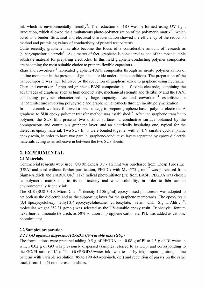
This deconvolution evaluation was performed on different aqueous GO dispersions varying both GO and PI content, in order to evaluate the best performing GO/PI ratio. The measurements prove the reduction of GO, with restoration of the extended conjugated sp2 structure. According to these results, the sample with GO/PI ratio of 1/4 gave the highest value of GO reduction. Several test patterns of the GOp formulations were inkjet printed on transparent substrates (microscope glass slides). Figure 2 shows an image of a glass substrate with inkjet printed straight lines of the GOp formulation with various thicknesses. The thickness of printed films was varied either by increasing the spotting resolution (variation of dpi) or repeating the same track in multiple passes, up to five

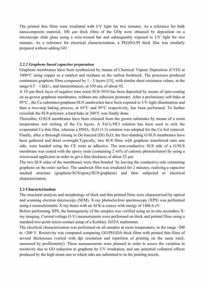
times. In particular, the repeated tracks showed a good uniformity and coverage of the substrate (inset in Fig. 2). The analysis of the microstructure of the printed tracks demonstrates that GO flakes distribute uniformly on the substrate and form a continuous layer with each other, ensuring continuity of electrical signal (Fig. 3). Figure 2: Image showing inkjet printed test tracks of the GOp ink on a microscope glass, after UV irradiation. Tracks with different thickness are shown, corresponding to variation of dpi resolution or several repetition of the printing. The inset shows an optical microscope magnification of a printed track with 125 dpi and 3 passes
Figure 3: SEM image showing the microstructure of an inkjet printed track of GOi suspension (water was evaporated before inserting the sample into SEM chamber). The inset shows a low-resolution image of the printed track

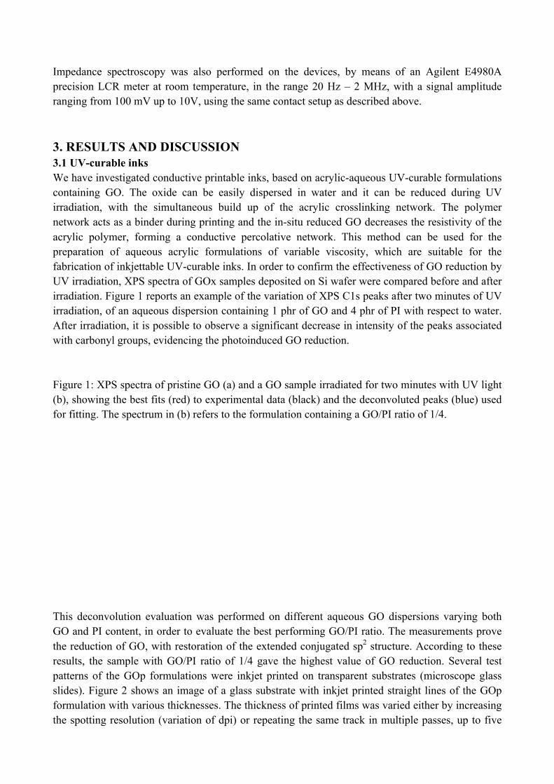
Figure 4 shows the resistivity of thin printed layer samples as a function of sample thickness, compared to thick films of GOp and pure PEDGA. Each experimental point in the plot is given by a computation based on linear fits to average I-V curves (error bars shown in the plot). The addition of GO to PEGDA, after reduction by UV irradiation, results in a decrease of resistivity by over an order of magnitude (GOp TF versus PEGDA TF). For what concerns printed samples, two trends may be evidenced, both concurring to a resistivity decrease. By increasing the number of passes and thus the track thickness, a small decrease of resistivity is obtained (green dashed arrow in fig. 4); this fact is normally due to an increased volume available for electrons’ drift. Furthermore, by decreasing the amount of ink spotted on a single-pass track (i.e. reducing the dpi resolution) and thus reducing the line thickness, a strong reduction of GO is obtained (blue solid arrow in fig. 4). Those samples show a decrease of resistivity by two orders of magnitude with respect to the pure matrix. This counter-intuitive fact may be explained considering that in a thin track a higher fraction of GO is reached and reduced by UV light than in a thick track, thus better contributing to electrical conduction. In fact, in the thick wire-wound bar-fabricated sample there should still exist a fraction of unreduced GO, possibly due to the complete absorption of UV radiation in a few micrometers at the top of the sample. Figure 4: Resistivity of GOp inkjet printed and thick film (TF) samples, as computed from linear fit to I-V curves, as a function of the sample thickness. Error bars are shown on experimental data points. The series refer to the inkjet printed tracks with single (blue solid arrow) and multiple (green dashed arrow) passes
3.2 graphene based capacitor The aim of this study was the preparation of transparent, thin and flexible organic capacitor starting from the graphene-polymer transfer method. Graphene membranes were synthesized on the Cu substrate obtaining a continuous graphene coating consisting of 1-3 layers, as clearly evidenced by the high-resolution TEM image reported in Figure 5.
Figure 5: TEM characterization of the graphene membranes. a) Low-magnification view of the CVD membrane transferred on a TEM grid with perforated carbon support film. b) High-resolution TEM (HRTEM) image detail of a folded edge, where the two (002) graphite fringes visible allows direct counting of the number of graphene layers composing the membrane.
Afterwards a 10 µm thick layer of SU8-3010 has been deposited on the few-layer graphene (FLG) membranes, by means of spin coating. Different thicknesses of SU8 layer can be also deposited, by changing spin-coating parameters. It has to be noted that direct spin-coating coupling of SU8 and graphene membranes allows for a better adhesion with respect to the laying commonly adopted strategy described above. As reported before, a baking and a subsequent curing processes have been performed in order to completely evaporate solvent and further crosslink the material for strengthening its mechanical properties. Then, by chemical etching in acid solutions the G/SU8 membranes have been released from the copper growth substrates. Finally, as the copper layer has been completely etched, the membranes can be easily scooped and washed in de-ionized water before being dried overnight at room temperature. The final G/SU8 membrane presents two distinct surfaces: one homogeneous conductive surface containing a graphene layer and one dielectric surface, typical of the epoxy polymer. Moreover, the G/SU8 membrane is highly transparent, with a transmittance higher than 90 % (see Figure 6). Two G/SU8 layers were bonded together by using an epoxy photocurable formulation based on CE in the presence of 2 wt% of the cationic photoinitiator. First of all the photocuring efficiency was monitored by RT-FTIR analyses, in order to evaluate if the UV light was able to pass through the G/SU8 film and efficiently promoting the UV-induced ring-opening polymerization of the epoxy resin employed as adhesive. For this reason the 25 µm epoxy formulation was coated on SiC wafer and covered with the modified G/SU8 film (of a thickness of about 10 µm). The decrease of the epoxy group band, centered at around 790 cm-1, as a function of irradiation time, provides an indication of the extent of the reaction; it was possible to monitor in real-time the epoxy group conversion and after 2 minutes of irradiation a plateaux conversion of about 85% was calculated. This is due to the well-known vitrification effect due to the formation of a crosslinked epoxy polymer network hindering the mobility of active groups while the reaction progresses. This results evidence the efficiency of UV-crosslinking of the epoxy resin, which could be used as UV-adhesive to bond the G/SU8 membranes.
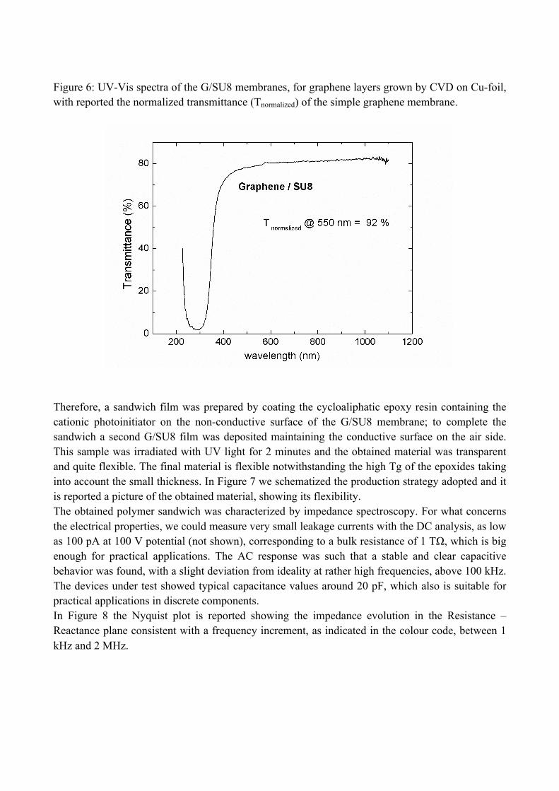
Figure 6: UV-Vis spectra of the G/SU8 membranes, for graphene layers grown by CVD on Cu-foil, with reported the normalized transmittance (Tnormalized) of the simple graphene membrane.
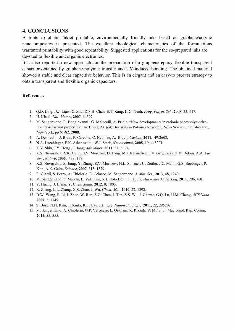
Therefore, a sandwich film was prepared by coating the cycloaliphatic epoxy resin containing the cationic photoinitiator on the non-conductive surface of the G/SU8 membrane; to complete the sandwich a second G/SU8 film was deposited maintaining the conductive surface on the air side. This sample was irradiated with UV light for 2 minutes and the obtained material was transparent and quite flexible. The final material is flexible notwithstanding the high Tg of the epoxides taking into account the small thickness. In Figure 7 we schematized the production strategy adopted and it is reported a picture of the obtained material, showing its flexibility. The obtained polymer sandwich was characterized by impedance spectroscopy. For what concerns the electrical properties, we could measure very small leakage currents with the DC analysis, as low as 100 pA at 100 V potential (not shown), corresponding to a bulk resistance of 1 TΩ, which is big enough for practical applications. The AC response was such that a stable and clear capacitive behavior was found, with a slight deviation from ideality at rather high frequencies, above 100 kHz. The devices under test showed typical capacitance values around 20 pF, which also is suitable for practical applications in discrete components. In Figure 8 the Nyquist plot is reported showing the impedance evolution in the Resistance – Reactance plane consistent with a frequency increment, as indicated in the colour code, between 1 kHz and 2 MHz.
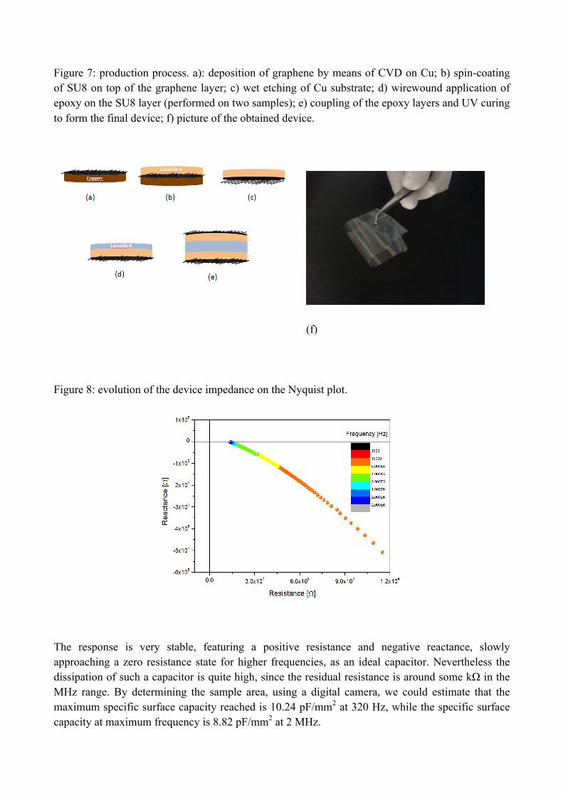
Figure 7: production process. a): deposition of graphene by means of CVD on Cu; b) spin-coating of SU8 on top of the graphene layer; c) wet etching of Cu substrate; d) wirewound application of epoxy on the SU8 layer (performed on two samples); e) coupling of the epoxy layers and UV curing to form the final device; f) picture of the obtained device.
(f)
Figure 8: evolution of the device impedance on the Nyquist plot.
The response is very stable, featuring a positive resistance and negative reactance, slowly approaching a zero resistance state for higher frequencies, as an ideal capacitor. Nevertheless the dissipation of such a capacitor is quite high, since the residual resistance is around some kΩ in the MHz range. By determining the sample area, using a digital camera, we could estimate that the maximum specific surface capacity reached is 10.24 pF/mm2 at 320 Hz, while the specific surface capacity at maximum frequency is 8.82 pF/mm2 at 2 MHz.
4. CONCLUSIONS A route to obtain inkjet printable, environmentally friendly inks based on graphene/acrylic nanocomposites is presented. The excellent rheological characteristics of the formulations warranted printability with good repeatability. Suggested applications for the so-prepared inks are devoted to flexible and organic electronics. It is also reported a new approach for the preparation of a graphene-epoxy flexible transparent capacitor obtained by graphene-polymer transfer and UV-induced bonding. The obtained material showed a stable and clear capacitive behavior. This is an elegant and an easy-to process strategy to obtain transparent and flexible organic capacitors.
References
1. Q.D. Ling, D.J. Liaw, C. Zhu, D.S.H. Chan, E.T. Kang, K.G. Neoh, Prog. Polym. Sci., 2008, 33, 917. 2. H. Klauk, Nat. Mater., 2007, 6, 397. 3. M. Sangermano, R. Bongiovanni , G. Malucelli, A. Priola, “New developments in cationic photopolymeriza-
tion: process and properties”. In: Bregg RK (ed) Horizons in Polymer Research, Nova Science Publisher Inc., New York, pp 61-82, 2008.
4. A. Denneulin, J. Bras , F. Carcone, C. Neuman, A. Blayo, Carbon, 2011, 49:2603. 5. N.A. Luechinger, E.K. Athanassiou, W.J. Stark, Nanotechnol, 2008, 19, 445201. 6. K.Y. Shin, J.Y. Hong , J. Jang, Adv Mater, 2011, 23, 2113. 7. K.S. Novoselov, A.K. Geim, S.V. Morozov, D. Jiang, M.I. Katsnelson, I.V. Grigorieva, S.V. Dubon, A.A. Fir-
sov , Nature, 2005, 438, 197. 8. K.S. Novoselov, Z. Jiang, Y. Zhang, S.V. Morozov, H.L. Stormer, U. Zeitler, J.C. Mann, G.S. Boebinger, P.
Kim, A.K. Geim, Science, 2007, 315, 1379. 9. R. Giardi, S. Porro, A. Chiolerio, E. Celasco, M. Sangermano, J. Mat. Sci., 2013, 48, 1249. 10. M. Sangermano, S. Marchi, L. Valentini, S. Bittolo Bon, P. Fabbri, Macromol Mater Eng, 2011, 296, 401. 11. Y. Huang, J. Liang, Y. Chen, Small, 2012, 8, 1805. 12. K. Zhang, L.L. Zhang, X.S. Zhao, J. Wu, Chem. Mat. 2010, 22, 1392. 13. D.W. Wang, F. Li, J. Zhao, W. Ren, Z.G. Chen, J. Tan, Z.S. Wu, I. Ghente, G.Q. Lu, H.M. Cheng, ACS Nano
2009, 3, 1745. 14. S. Bose, N.H. Kim, T. Kuila, K.T. Lau, J.H. Lee, Nanotechnology, 2011, 22, 295202. 15. M. Sangermano, A. Chiolerio, G.P. Veronese, L. Ortolani, R. Rizzoli, V. Morandi, Macromol. Rap. Comm,
2014, 35, 355.