Embed Size (px)
Citation preview

State of the Art and Future Trends in Radiation
Detection for Computed Tomography
Ami Altman, PhD, PHILIPS Science Fellow
Global Research & Advanced Development
CT BU, PHILIPS Healthcare

Ami Altman, Ph.D., PHILIPS Healthcare 2
1. Conventional, state of the art, and future CT
detection system
2. A Dual-Layer detector for a Detector- Based Spectral
CT, with some applications’ examples
3. Photon-Counting Spectral CT detectors, advantages,
opportunities, and risks
Plan

Ami Altman, Ph.D., PHILIPS Healthcare 3
A Little About CT Present CT
1. Large Coverage Detector
2. Wedge Configuration
3. Fast Rotation (close to 0.25
sec/Rot.)
4. 2D Focal-Spot double sampling
5. Very Short angular sampling time
(~100 µsec)
6. High-Rate and Power X-Ray Tubes
7. Sub-Millimeter isotropic resolution
8. Very good temporal resolution
9. A 3D and 4D imaging devise
(Space-Time)

Ami Altman, Ph.D., PHILIPS Healthcare 4
X-Ray Tube
Detection Array System
X-Ray Generators
Couch
Beam Shaping Collimator
So How Does It Look Like in Reality?

Ami Altman, Ph.D., PHILIPS Healthcare 5
Photodiode:
Light to Electric Current
Scintillator
Converts X-ray to Light
Current
Integration
A/D
t
Readout ASIC
X-Ray in
Pixelated CT Detector – Basic Pixel Structure & Requirements
Modern CT Detectors Requirement
Frame Rate & size 10,000 frames/sec
~120,000 pixels/frame
Detector Readout Mode Current (energy) Integration
Electronic noise RMS < 3 pA
High light output
scintillator
Ceramic Gd2O2S (GOS) (~40,000
photons/MeV)
Low Scintillator Afterglow <200 ppm at 3 m-sec
<20 ppm at 500 m-sec
expandable configuration 4-sides tile-able arrays
Spatial Resolution ~24 lp/cm (~0.210 mm)
Scattering rejection SPR < 5%; 2D Anti-Scatter-Grid
Maximum Crosstalk
(optical & elec)
~5%
Pixelated Si photodiode
with excellent response
> 0.35 A/Watt for = 514 nm
Dynamic Range ≥ 220
Scintillator Stopping
power
> 98% for 120 kVp specctrum Signal Pixel ∝ Total X-Ray Energy
absorbed in the scintillator
within a sampling time.

Ami Altman, Ph.D., PHILIPS Healthcare 6
Pixelated Large-Area Photodiode for CT Detector
Front-illuminated photodiode: anodes
directly illuminated ; limited expandability
Back illuminated “64 slices” photodiode
“flip-chipped” to a substrate
Pitch between lines
=L / M
Column 1
Column 2
Column N
Active area for a pixel
L
W
A 2M x N Photodiode array
Pitch 11 m
Pitch between lines
=L / M
Column 1
Column 2
Column N
Active area for a pixel
L
W
A 2M x N Photodiode array
Pitch 11 m
Column 1
Column 2
Column N
Active area for a pixel
L
W
A 2M x N Photodiode array
Pitch 11 m
Si Photodiode response

Ami Altman, Ph.D., PHILIPS Healthcare 7
Scintillator Arrays for CT, Material types
CT Scintillators in Use, (Potential Use)
Scintillator Light-yield
(#
photons/M
eV)
Form: Ceramic
\
Single Cristal
Afterglow Comment
Gd2O2S:Pr,Ce (GOS) ~40,000 Ceramic; semi
translucent
low Most vendors; some
doping variations
GE GemstoneTM ( a Lu
based Garnet)
~40,000 Ceramic;
translucent
low
Garnet type of
(Lu,Gd,Y,Tb)3(Ga,Al)5O12
40,000-
45,000
Ceramic;
translucent
low Fast rise time
(Y,Gd)2O3:Eu
(GE HiLightTM )
Ceramic high not adequate for short
Integration Periods
ZnSe:Te
(low stopping power)
~65,000 Single Cristal; semi-
translucent
low In Philips Dual-Layer
CT prototype
MeVphotonsE
LimitYieldLightg
/5.2
10__
6
GOS ZnSe
NOTE: Light output is smaller than Light-Yield
because of Internal absorption & Reflections

Ami Altman, Ph.D., PHILIPS Healthcare 8
Philips Brilliance-64 Module W\O and
with anti-scatter grid
Pixelated Scintillators, and CT DAS Assembly Modes
ZZ
BIP
scintillator
Ceramic substrate
PD
substrate
ASIC
Heat
Sink
Anti-
Scatter
scintillator
Tile Concept
X
Z
X
Z
PHILIPS iCT-256, Tiled Config. , 2D anti-scatter grid
Tiled Module 2D-Anti-Scatter grid

Ami Altman, Ph.D., PHILIPS Healthcare
1. Detector-Pixel signal at each sampling is assumed to represent a line
integral of the form:
that assumes X-Ray pure-transmission only.
2. Allowing scattered radiation Cupping and blackened streaks
artifacts between scattering centers:
9
Why Anti Scatter Grids in CT Detectors ?
out
in
dII
)()ln()ln() ,P( 0
SW Scatter-artifacts Correction effect!
Note the significant noise increase. 1D VS. 2D Anti-Scatter Grid

Ami Altman, Ph.D., PHILIPS Healthcare 10
𝐷𝑄𝐸 =𝑆𝑁𝑅𝑜𝑢𝑡
2
𝑆𝑁𝑅𝑖𝑛2 𝐷𝑄𝐸 𝑓 ≅
𝑆2 𝑀𝑇𝐹2 𝑓
𝑁𝑃𝑆 𝑓 ∙ ∅ , or measured:
(S=detector signal; = # of photons per area unit; NPS=
Noise Power Spectrum)
Estimated upper limits of MTF and various CT parameters
contribution to it in standard resolution mode (Philips
iCT-256), assuming Sinc function response:
A measured single pixel MTF and DQE (PHILIPS tile detector), (including Swank Noise and Crosstalk (R
Luhta et al. SPIE-2006)
Overall Detection Efficiency (DE) has to include the Geometrical
Detection Efficiency (GDE) , determined by the fraction of active area
to total pixel area in the pixelated scintillator (~73%).
DQEGDEDE
MTF, DQE and Detection Efficiency, as CT Detectors Metrics

Ami Altman, Ph.D., PHILIPS Healthcare 11
MTF Improvement – Crosstalk & Afterglow Corrections
Correcting for Pixel Crosstalk, and Scintillator
Afterglow through deconvolution method
(Philips Brilliance 16), in an Ultra-High
Resolution Mode (slice plane)
Measured Detection-Pixel crosstalk and
deviation from pure square wave response due
to crosstalk.
(R. Luhta et al, SPIE-2006)
(See R. Carmi et al. Nuclear Science Symosiom
conference record 2004, 5:2765-2768.)

Ami Altman, Ph.D., PHILIPS Healthcare 12
Effect of Electronic Noise in Energy-Integrated CT Detector
0 5 10 15 20 25 30 35 40 45 5010
-1
100
101
102
103
104
105
Dixel signal (X-ray photons) vs. object thickness for tube currents 30-210 mA
rad. path through scanned object (cm)
Dix
el S
ign
al , N
ois
e (
# o
f X
-ray p
ho
ton
s)
30 mA
60 mA
90 mA
120 mA
150 mA
180 mA
210 mA
0 5 10 15 20 25 30 35 40 45 5010
-13
10-12
10-11
10-10
10-9
10-8
10-7
PD current vs. object thickness for tube currents 30-210 mA
rad. path through scanned object (cm)
PD
cu
rren
t (A
)
30 mA
60 mA
90 mA
120 mA
150 mA
180 mA
210 mA
Photodiode’s current as a function of
absorption path (water), and Tube current
Detector’s radiation signal and total noise as
a function of absorption path in water, and
Tube Current
• An exaggerated RMS noise of 5 pA has been taken in account, just for
demonstration
• Today’s readout ASICS which are assembled attached to the photodiodes have
RMS noise < 3 pA
• In most read-out electronics, both Sigma-Delta, or Current-to-Frequency, the
RMS noise increases slightly for shorter integration periods

Ami Altman, Ph.D., PHILIPS Healthcare 13
Low Dose Artifacts (rings), introduced by Electronic Noise
and Non-Linear Effects
1. 50-cm water phantom
2. Old version Electronics
Philips BR-64 (non-tiled)
3. Scanned at 0.4 sec/rot., with
70 mAs
4. Measured RMS noise ~5pA
5. Artifacts caused mainly by
electronics non-linear
effects and offset stability
during the scan

Ami Altman, Ph.D., PHILIPS Healthcare 14
0.080 mm reflecting paint
0.030 mm optical glue
A 0.125-mm side-looking photodiode array
shielded by a 0.5 mm Tungsten layer
Bottom
Scintillator:
2-mm GOS
Top Scintillator,
1.0 mm
X-Rays Coming from top
X
Y
(e.g. ZnSe)Low Energy Raw data
High Energy Raw data
~50%
~50%
E1 image
E2 image
+
CT imageWeighted combined Raw data=
Dual-Energy Spectral CT Based on A Dual-Layer Detector
A 16 X 16 pixels Dual-Layer Detector
Tile for A Dual-Energy Spectral CT
Stacking Dual-Layer 1-D
arrays into a single
standard detection tile

Ami Altman, Ph.D., PHILIPS Healthcare 15
Zeff_1 > Zeff_2 > Zeff_3
E-High (HU)
E-Low (HU)
Zeff_3
Zeff_2
Zeff_1
Water (E_low & E_high = 0 HU)
A phantom with different concentrations of
Calcium and Iodine contrast agent
µ_E
_L
ow
(HU
)
µ_E_High (HU)
Iodine
Calcium
zoom
water
Conventional CT Image
3
3
2.0,E
ZB
E
ZAEZ
HU of E1
HU of E2
Soft Tissue
Calcium & Bones
Iodine-tagged Blood
Fat
IodineCalcium
Soft tissue
Conventional CT Image Spectral CT Image, Dual-E
Spectral Analysis Map
Dual Layer Detector Data Representation – Image Domain

Ami Altman, Ph.D., PHILIPS Healthcare 16
Siemens GE Philips
Technology Path Two-tube Two-Detector
configuration
One tube with fast kV
switching
One tube, detectors with
simultaneous high and low
energy discrimination
Full FOV Limited (~35 cm) Full (50 cm) Full (50 cm)
High/Low Energy
Separation +
Projection Space
Reconstruction
Tube Current
Modulation
Low/High Energy Image
Reconstruction
Retrospective Dual-E
Analysis, all protocols
Dual-Energy Technologies – Various Vendors

Ami Altman, Ph.D., PHILIPS Healthcare 17
Material Separation
• Direct CTA
• Gout Diagnosis
• Prep-Less CT Colonography
Material Quantification
• Virtual Non-Contrast
• Blood Flow Iodine Perfusion (PE)
• Lesion Uptake & Volume Assessment
• Plaque Characterization
• Cardiac CT
• Urinary Stone Characterization
Monochromatic Imaging
• Salvaging Sub-Optimal CTAs
• Optimum CNR Imaging (↑Lesion visualization)
• Metal & Beam Hardening Reduction
• Effective Atomic Number
17
Dual-Layer Spectral CT – Main Clinical Applications
Ami Altman, Ph.D., PHILIPS Healthcare 18
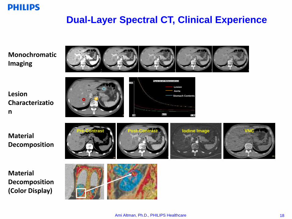
Lesion
Aorta
Stomach Contents
Pre-Contrast Post-Contrast Iodine Image VNC
Monochromatic Imaging
Lesion Characterization
Material Decomposition
Material Decomposition (Color Display)
Dual-Layer Spectral CT, Clinical Experience

Ami Altman, Ph.D., PHILIPS Healthcare 19
Dual-Layer Spectral CT, Viewer Screen Shot Example

Ami Altman, Ph.D., PHILIPS Healthcare 20
Photon-Counting Spectral CT – Photon-Counting Detector
Conventional Detector
Integrated Energy
(white light intensities)
Photo Diode
Integrating ASIC
Scintillator
X-Ray Photons
Direct Conversion Detector
Spectral Profile
(Discrimination and counts)
Photo Diode
Counting ASIC
High energy
photons hit a
semiconductor
and are directly
converted to an
analog signal
A fast ASIC
translates
individual signal
pulses to counts
at several energy
bins
Direct Conversion Material
e h e
h
e h
~ 13,000 e-hole
pairs per 60 keV
photon
~ 1
00
0 e
-ho
le
pa
irs
pe
r 6
0 k
eV
ph
oto
n in
th
e
ph
oto
dio
de

Ami Altman, Ph.D., PHILIPS Healthcare 21
Cu
rren
t Inte
gra
tion
Mo
de
Current
Integration
A/D
p+
n+
Scintillator
Non-biased photodiode
Incident X-Rays
X-ray to Visible Light
Conversion (GOS512 nm)
Light-to-Current
Conversion
t
Output integrated energy
absorbed in a detector element
within a single Integration Period
FEE
ASIC
e-h+
A Current-Integration CT
Detector
A Photon-Counting, Direct-Conversion, CT Detector
1-mm and 0.5-mm detector pitch
(CdZnTe) (IMARAD\OMS IEEE 2009):
PhC Requires much smaller
pixels to enable CT
radiation rates
Photon Counting Detector Direct Conversion VS Energy Integration
Absorbed single X-ray photon
High
Voltage
Counter 3
Counter 2
Counter 1
Counter 4
Charge pulse
Pulse height proportional
to x-ray photon energy
Discriminating
thresholds
Stored counts of all energy windows,
for each reading time period
Direct conversion
material
Electronics
Pixelated electrodes
Photon energy
Counts
Photon Counting Spectral CT – Detector Principle
Direct- Conversion Detector efficiently translates X-ray photons into large electronic signals
These signals are binned according to their corresponding X-ray energies
Operation Principles – A CT Photon-
Counting Detector

Ami Altman, Ph.D., PHILIPS Healthcare 22
Muscle
Water
Plexiglas
8 bins of 11-keV each:
1/E3 weightingEnergy IntegrationPhoton-Counting
total (no energy bins weighting)
bins
bins
N
i
icph
N
i
icph
k
kS
1
2
..
1
..
1
1
0
2
1
2
01
)(
)(
dEEwEkE
dEEwEkES
N
i
iiEI
N
i
iiEI
0
2
4
6
8
10
12
0 50 100 150
Wei
ghti
ng
(no
n-n
orm
aliz
ed )
Energy (keV)
E.I.
P.C.
P.C. 1/E3
1. Z_eff of Plexiglas is ~20% < water
2. Energy Integrating over weights
density over Z.
3. Photon Counting changes HU ratios,
Contrast difference, and CNR
4. Opportunity to adapt energy
weighting to specific applications
5. Potential increase in soft-tissue
resolution.
The Photon Counting Energy Weighting “Miracle”

Ami Altman, Ph.D., PHILIPS Healthcare 23
Where Dual-Energy CT Fails – The Need for More than
2 Energy Bins.
I – iodine
Gd – gadolinium
Ca – calcium (as CaCl)
H – high concentration
L – low concentration
C –solid carbon
A –air bubbles (in foam)
-100 0 100 200 300 400 500 600
50
100
150
200
250
300
350
400
450
500
I-H
Gd-HCa-H
Gd-L
I-L
Ca-L
CC
CC
C
C
AA
AA
A
A
Water
-100 0 100 200 300 400 500 600
50
100
150
200
250
300
350
400
450
500
I-H
Gd-HCa-H
Gd-L
I-L
Ca-L
CC
CC
C
C
AA
AA
A
A
Water
7 cm
(Measured in a Rotating Table Photon Counting
Mini CT, PHILIPS Healthcare, Haifa)
0 100 200 300 400 500
50
100
150
200
250
300
350
400
450
500
2 spectral windows:
25-46, 85-125 keV
0 100 200 300 400 500
50
100
150
200
250
300
350
400
450
500
6 spectral windows:
25-46, 46-54, 54-65, 65-75, 75-85,
85-125 keV
Iodine
Calcium Chloride
Gadolinium
Carbon
Water
Mixtures or interfaces of more than 2 materials,
suffers from spectral partial volume, distorting
material decomposition and classification

Ami Altman, Ph.D., PHILIPS Healthcare 24
So Where is The Catch, Why CT is Not Transforming to
Photon-Counting Detector?
1. Best Candidates, CdTe and CdZnTe (CZT) are not easy to manufacture, to meet CT
requirements
2. Detector Polarization (eliminating or distorting the electric field inside the detector,
stopping any signal output), mainly caused by traps and impurities in the crystal
lattice
3. Charge sharing between close neighboring pixels, causing low energy tail, that
distorts measured energy spectrum, especially for a wideband spectrum like in CT
4. Te and Cd fluorescence K-escapes to neighbor pixels and from neighbor contributing
to the low-energy tail
5. Pile-Up already at relatively low rate
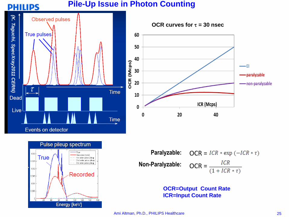
Ami Altman, Ph.D., PHILIPS Healthcare 25
Paralyzable:
Non-Paralyzable:
OCR=Output Count Rate
ICR=Input Count Rate
Pile-Up Issue in Photon Counting
OCR curves for = 30 nsec
(K. T
ag
uc
hi, S
pe
cX
ray
2011 C
ER
N)

Ami Altman, Ph.D., PHILIPS Healthcare 26
DQE(0) in Photon Counting Detectors
Yu and Fessler in Phys. Med. Biol. 45 (2000) 2043-2056.
For Variance estimates see

Ami Altman, Ph.D., PHILIPS Healthcare 27
Low-Energy Tail and its effect on Spectral CT Quality
CdTe arrays: Spectral
response to Am241
source (59.5 keV)
CdTe arrays: Spectral
Response to a 110 kVp X-
Ray Tube
Figures taken from
T. Koenig et al
Phys. Med. Biol. 57 (2012) 6743–6759

Ami Altman, Ph.D., PHILIPS Healthcare
Pre-clinical spectral CT scanner platform
• Gantry with rotation speed up to 1/3 s per turn
• -Focus X-ray tube
– 40 kVp - 130 kVp
– max. 65W
• CdTe-based Photon-Counting detector
– 0.4 mm pixel pitch, 1024 pixel along X
– 6 energy bins per pixel
• Magnification: 2 - 6
• Field-of-view: 6 cm - 23 cm
• Spatial Resolution: 100 m - 250 m
Scanner copy: Washington University, St. Louis
G. Lanza, S. Wickline
First scanner: Philips Research Hamburg
28

Ami Altman, Ph.D., PHILIPS Healthcare 29
Enabling K-Edge Imaging
and Targeted CT Imaging (PHILIPS – Mount Sinai
Collaboration)

Ami Altman, Ph.D., PHILIPS Healthcare 30
30 30 30
Anatomical mouse image with Iodine concentration overlay
Human carotid samples with targeted contrast agent
Artificial calcification inside of a stent.
Left: integrated CT image, Right: photo- and Gd image
Hepatis steatosis (fatty liver)
phantom measurements
Washington University Collaboration
Imaging nano particles, loaded
with Gadolinium & Bismuth, and
targeted mainly to fibrin in soft
plaque

Ami Altman, Ph.D., PHILIPS Healthcare 31 31 31
imaging results From collaboration with Eindhoven
Tail cross section
Quantification
• iodinde-based
bloodpool agent
• mouse images

32
Applications demand high delivered payloads of heavy metals targeted to
intraluminal thombus, but excluded from intraplaque fibrin.
NanoK targeted to thrombus in situ. Systemic targeting
studies on-going in vivo
Nanoparticles home specifically to intra-lumenal fibrin
not intramural fibrin from healed hemorrhage or
rupture
(in vitro CEA specimens from Patient)
fluorescence microscopy optical microscopy
Pan, Roessl, Thran,…Proksa, et. al. Angew Chem Int Ed. 2010, 9635-39
Bismuth Nanobeacons Target Fibrin of Thrombus on Ruptured Plaque
Investigating K-Edge Imaging at WashU

33
Pan, Schirra, Roessl, Thran, … ,Proksa et al., ACS Nano. 2012 (in press, e-pub available)
Investigating K-Edge Imaging at WashU Imaging of new Ytterbium Nanobeacons

Ami Altman, Ph.D., PHILIPS Healthcare 34
Consequences
1. Innovative detectors technologies has lead, and will lead future CT
evolution and revolution towards quantitative imaging in more than
just anatomy and morphology.
2. Detector-based spectral CT enables the benefit of material\tissue
analysis retrospectively for all conventional protocols, without the
need to decide on a specific Dual-Energy protocol.
3. Photon-Counting detectors for spectral CT imaging is a promising
technology, that offers also much better spatial resolution, no
electronic noise, better CNR, capability to further reduce dose, and a
more accurate material and tissue representation and decomposition.
4. Photon-counting CT may open an opportunity to use targeted contrast
agent, thus become more quantitative, enabling more personalized
diagnostics.
5. We are not yet there. There are several significant technology
challenges, in detector performance and pile up issues, to overcome.


![REVIEW OpenAccess Recentdevelopmentsintime-of-flightPETners580/ners-bioe_481/lectures/pdfs/2016-02-EJN… · [43]. Another most recent TOF-PET/CT system, Vereos Digital, is developed](https://img.pdfslide.us/doc/110x75/605b0ee8e4a8670fa82496e8/review-openaccess-recentdevelopmentsintime-of-ners580ners-bioe481lecturespdfs2016-02-ejn.jpg)