Embed Size (px)
Citation preview
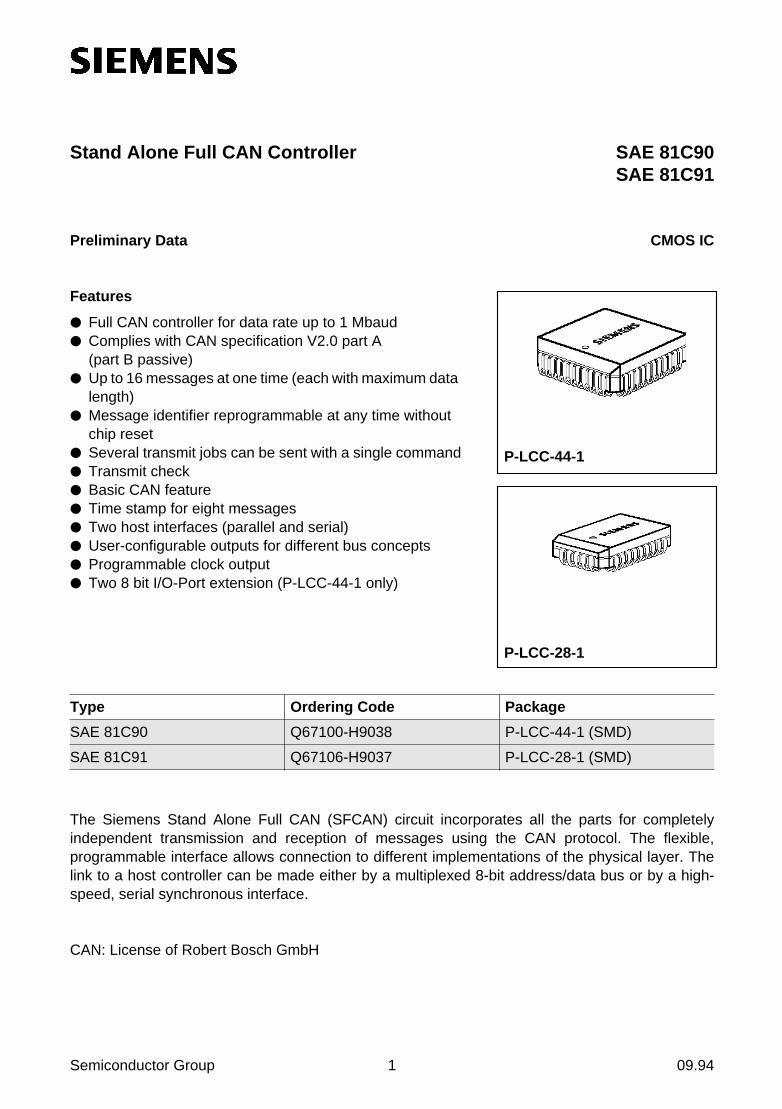
The Siemens Stand Alone Full CAN (SFCAN) circuit incorporates all the parts for completelyindependent transmission and reception of messages using the CAN protocol. The flexible,programmable interface allows connection to different implementations of the physical layer. Thelink to a host controller can be made either by a multiplexed 8-bit address/data bus or by a high-speed, serial synchronous interface.
CAN: License of Robert Bosch GmbH
Type Ordering Code Package
SAE 81C90 Q67100-H9038 P-LCC-44-1 (SMD)
SAE 81C91 Q67106-H9037 P-LCC-28-1 (SMD)
Stand Alone Full CAN Controller
Preliminary Data CMOS IC
SAE 81C90SAE 81C91
Features
Full CAN controller for data rate up to 1 Mbaud
Complies with CAN specification V2.0 part A(part B passive)
Up to 16 messages at one time (each with maximum data length)
Message identifier reprogrammable at any time without chip reset
Several transmit jobs can be sent with a single command
Transmit check
Basic CAN feature
Time stamp for eight messages
Two host interfaces (parallel and serial)
User-configurable outputs for different bus concepts
Programmable clock output
Two 8 bit I/O-Port extension (P-LCC-44-1 only)
Semiconductor Group 1 09.94
P-LCC-44-1
P-LCC-28-1
SAE 81C90SAE 81C91
Semiconductor Group 4
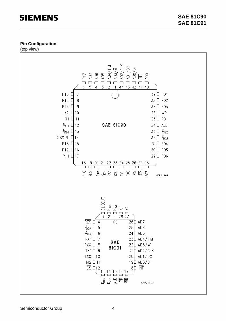
Pin Configuration
(top view)
SAE 81C90SAE 81C91
Semiconductor Group 5
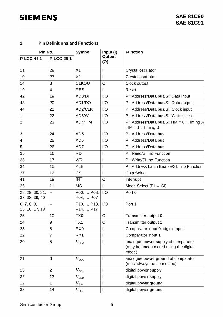
1 Pin Definitions and Functions
Pin No. Symbol Input (I) Function
P-LCC-44-1 P-LCC-28-1 Output (O)
11 28 X1 I Crystal oscillator
10 27 X2 I Crystal oscillator
14 3 CLKOUT O Clock output
19 4 RES I Reset
42 19 AD0/DI I/O PI: Address/Data bus/SI: Data input
43 20 AD1/DO I/O PI: Address/Data bus/SI: Data output
44 21 AD2/CLK I/O PI: Address/Data bus/SI: Clock input
1 22 AD3/W I/O PI: Address/Data bus/SI: Write select
2 23 AD4/TIM I/O PI: Address/Data bus/SI:TIM = 0 : Timing ATIM = 1 : Timing B
3 24 AD5 I/O PI: Address/Data bus
4 25 AD6 I/O PI: Address/Data bus
5 26 AD7 I/O PI: Address/Data bus
35 16 RD I PI: Read/SI: no Function
36 17 WR I PI: Write/SI: no Function
34 15 ALE I PI: Address Latch Enable/SI: no Function
27 12 CS I Chip Select
41 18 INT O Interrupt
26 11 MS I Mode Select (PI
↔
SI)
28, 29, 30, 31,37, 38, 39, 40
– P00, … P03,P04, … P07
I/O Port 0
6, 7, 8, 9,15, 16, 17, 18
– P10, … P13,P14, … P17
I/O Port 1
25 10 TX0 O Transmitter output 0
24 9 TX1 O Transmitter output 1
23 8 RX0 I Comparator input 0, digital input
22 7 RX1 I Comparator input 1
20 5
V
DDA
I analogue power supply of comparator(may be unconnected using the digital mode)
21 6
V
SSA
I analogue power ground of comparator(must always be connected)
13 2
V
DD1
I digital power supply
32 13
V
DD2
I digital power supply
12 1
V
SS1
I digital power ground
33 14
V
SS2
I digital power ground
SAE 81C90SAE 81C91
Semiconductor Group 6
2 General Description
The Siemens stand-alone Full-CAN (SFCAN) circuit is a large-scale-integrated peripheral devicethat executes the entire protocol of an automobile or industrial network.
Bus communication is based on the controller-area-network (CAN) protocol. With features like shortmessage length, guaranteed reaction time for messages of appropriate importance, priority of busaccess defined by message identifiers, powerful error detection and treatment plus ease ofoperation, the CAN protocol is optimally designed for the requirements of automobile and industrialelectronic networks.
The SFCAN circuit incorporates all the parts for completely independent transmission and receptionof messages using the CAN protocol. The flexible, programmable interface allows connection todifferent implementations of the physical layer. The link to a host controller can be made either bya multiplexed 8-bit address/data bus or by a high-speed, serial synchronous interface.
The device comes in two versions: SAE 81C90 in a P-LCC-44-1 package with two 8-bit l/O ports,and SAE 81C91 in a P-LCC-28-1 package without l/O ports.
2.1 Main Features
Multi-master capability
Assignment of message priorities for high priority messages
Guaranteed reaction time
Flexible configuration
Several receivers simultaneously
System-wide data consistency
Resolution of bus accesses without time losses (arbitration)
High data rates up to 1 Mbaud
Error detection with automatic repeated transmission of disturbed messages
Discrimination between temporary and permanent errors, automatic, disconnection of defectivestations
Complies with CAN specification V2.0 part A (part B passive= messages according to part B aretolerated but not latched)
Extra check of data from CPU and transmitted data for equality (transmit check)
Up to 16 messages at one time with maximum data length
Message identifier reprogrammable at any time without chip reset
Several transmit jobs can be sent with a single command
One message memory can be configured so that all messages are received except thosecovered by other memory locations (monitor function, basic CAN feature)
Time stamp for eigth messages for rating actuality or repetition rate of messages
User-configurable outputs for different bus concepts
Programmable clock output
SAE 81C90SAE 81C91
Semiconductor Group 7
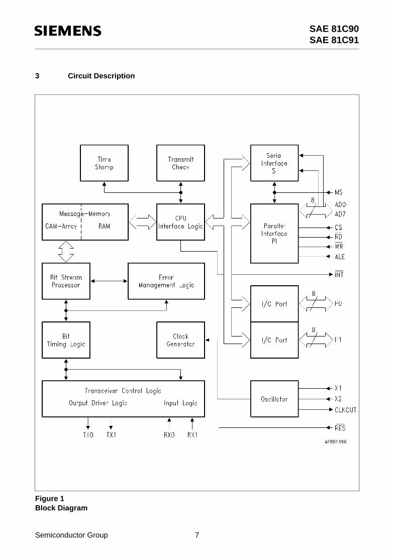
3 Circuit Description
Figure 1Block Diagram
SAE 81C90SAE 81C91
Semiconductor Group 8
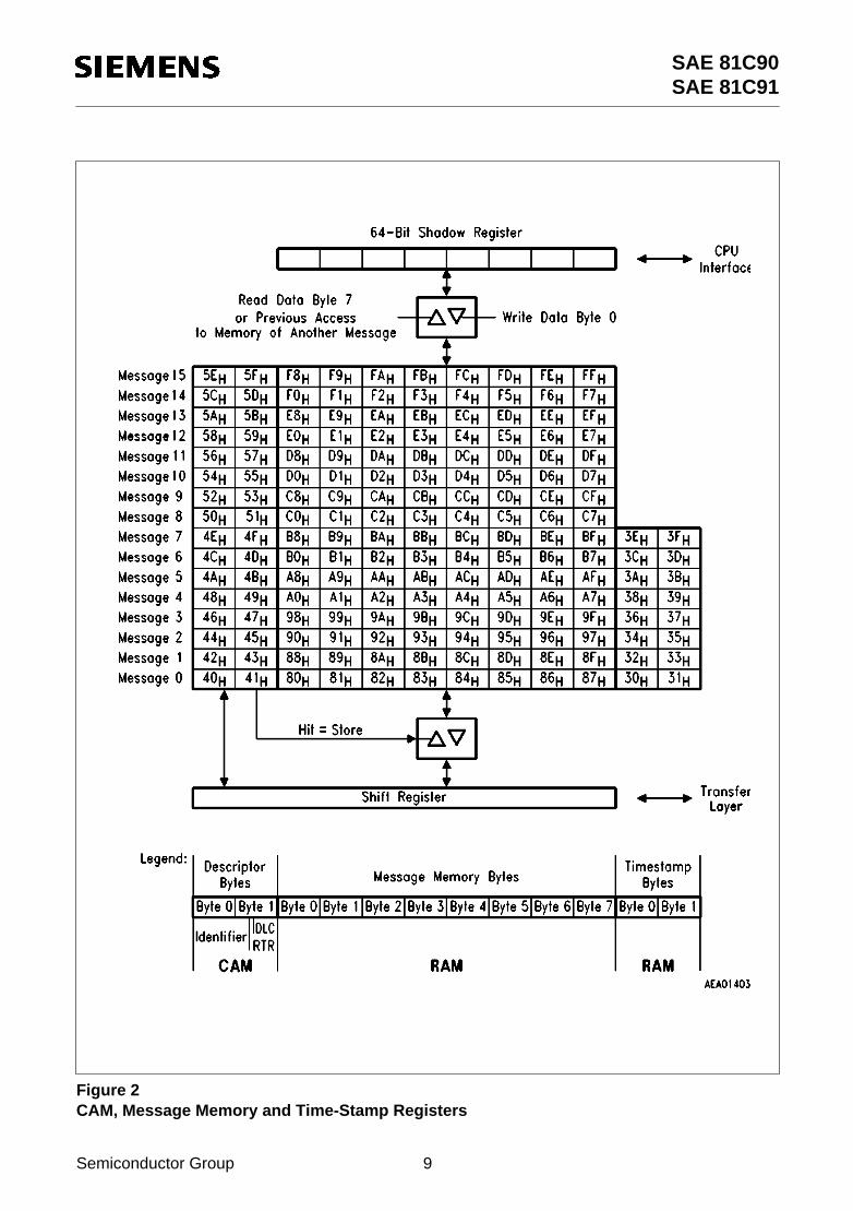
3.1 Message Memory
The SFCAN circuit filters incoming messages with an associative memory (CAM = content-addressable memory). For this the identifier and RTR bits of the required message must be writtento the appropriate memory location.
The identifier of each incoming message is compared to the identifiers held in CAM. When equalityis detected, the received data bytes are written into the matching RAM location. At the same timethe corresponding receive-ready bit is set and a receive interrupt is generated, if it is enabled. If nomatch is detected, the received message is rejected.
Identifiers can be reprogrammed at any time, although it is possible that data of the old or newidentifier may be lost during reprogramming.
An incoming transmit request will only be satisfied automatically by the hardware if the RTR bit ofthe particular identifier is set in CAM.
To ensure data consistency when reading or writing several data bytes, these data are buffered ina 64-bit shadow register (
see Figure 2
'CAM, Message Memory and Time-Stamp Registers' on thenext page).
Writing must start with the most-significant data byte. When data byte 0 is written, the contents ofthe shadow register are transferred in parallel into the RAM of the appropriate memory location. Inreadout the data are transferred into the shadow register automatically by interpreting the addressof the byte that has just been read. In this way, for example, reading address 83H insures that thedata of address 80H through 87H go into the shadow register. But transfer is only made if a date ofanother message has been read out beforehand. Upon readout of the higher-level data byte (e.g.address 87H) the shadow register is newly loaded in any case.
For these reasons it is absolutely essential to insure the writing of data is not interrupted by a readoperation and vice versa, a read operation should not be interrupted by a write.
SAE 81C90SAE 81C91
Semiconductor Group 9
Figure 2CAM, Message Memory and Time-Stamp Registers
SAE 81C90SAE 81C91
Semiconductor Group 10
3.2 Bit Stream Processor (BSP)
The bit-stream processor controls the entire protocol, differentiates between the frames types anddetects frame errors.
3.3 Error Management Logic (EML)
The error-management logic receives error messages from the BSP and, in turn, sends backinformation about error state to the BSP and CIL.
3.4 Bit Timing Logic (BTL)
The bit-timing logic determines the timing of the bits and synchronises with the edges of the bitstream on the CAN bus.
3.5 Transceiver Control Logic (TCL)
The transceiver-control logic consists of programmable output driver, input comparator and inputmultiplexer.
3.6 Clock Generator (CG)
The clock generator consists of an oscillator and a programmable divider. The oscillator can be fedfrom an external quartz crystal, ceramic resonator or an external timing source. The permissiblecrystal frequency is 1 to 20 MHz, and the external clock may be between 0 and 20 MHz. Aprogrammable frequency, dependent on the crystal clock, is available with the CLKOUT pin, e.g. forthe clocking of a host controller.
3.7 CPU Interface Logic (ClL)
The CPU interface logic controls the access of the host via the parallel or serial interface, interpretsthe commands and outputs status and interrupt information.
3.8 Transmit Check
The CAN protocol insures a very large integrity for the data transferred over the bus. The on-chippath from the data stored in parallel to the serial bit stream is not protected by the protocol however.To eliminate any possible uncertainties at this point too, the SFCAN circuit incorporates a transmit-check unit. This reads back a transmitted message via the normal receive path from the businterface and compares the data to those written into the message memory by the host controller.If any inconsistency of the data is detected, the current message will be invalidated by an errorframe.
The transmit-check error counter TCEC is then incremented by 1. If this counter reaches 4, an errorinterrupt (bit TCI in the INT register) is generated, provided that this has not been masked (bit ETCIin the IMSK register). This count will also produce the bus-off status.
The TCEC is set to 0 after a reset and can be read and also written for test purposes at any time.
Note:
The transmit-check is an additional feature of the Siemens Full CAN Chip and is not part of CAN protocol.
SAE 81C90SAE 81C91
Semiconductor Group 11
3.9 Time Stamp
Normally it is impossible to determine from the received data in the message memory when theywere received. So the host controller is unable to derive any information about the actuality or therepetition rate of the data.
To enable an indication of the time of reception for at least some of the messages, there is a 16-bittimer implemented on the SFCAN circuit. The content of this is written into the time-stamp registersof the particular message when it is received in the memory locations of messages 0 through 7.There are two time-stamp bytes for each of the messages 0 through 7, and these hold the value ofthe 16-bit timer.
The actuality of a message is determined by subtracting the old time-stamp of a message, storedin the host controller, from the new one, with respect to the timer overflow bit.
Overflow of the timer can be detected by bit TSOV in the CTRL register. This bit does not trigger aninterrupt and has to be reset by the host controller. Depending on the setting of bits TSP0 and TSP1in the CTRL register, the counter is fed with 1/32, 1/64, 1/128 or 1/256 of the bus clock. Themomentary timer status can be read and set at any time. The timer starts at 0 after a reset andcannot be stopped.
3.10 I/O-Ports
There are two parallel I/O ports in the SAE 81C90, each with eight pins. These ports are configuredpin by pin as input or output, depending on the contents of the port-direction register.
The output data for the port pins can be written (latched) into the port-latch register. Reading thisregister reproduces the contents of the latch. The levels on the port pins can be read from the port-pin register.
For the SAE 81C91 in its P-LCC-28-1 package, the pads of the I/O ports are not bonded andtherefore unavailable to the user.
3.11 Control Registers
The SFCAN circuit is controlled by registers. These can be accessed by the addresses listed below.If not otherwise noted in the detailed description, they are readable and writeable.

SAE 81C90SAE 81C91
Semiconductor Group 12
Address Assignments: Control Registers
Addresses not listed above are not available and must not be written in initialisation mode.
Register Name Address Function
BL1 00H Bit-length register 1
BL2 01H Bit-length register 2
OC 02H Output-control register
BRP 03H Baud-rate prescaler
RR1 04H Receive-ready register 1
RR2 05H Receive-ready register 2
RIM1 06H Receive-interrupt-mask register 1
RIM2 07H Receive-interrupt-mask register 2
TRS1 08H Transmit-request-set register 1
TRS2 09H Transmit-request-set register 2
IMSK 0AH Interrupt-mask register
REC 0CH Receive-error counter (for test only)
TEC 0DH Transmit-error counter (for test only)
MOD 10H Mode/status register
INT 11H Interrupt register
CTRL 12H Control register
CC 14H Clock-control register
TCEC 15H Transmit-check error counter
TCD 16H Transmit-check data register
TRR1 18H Transmit-request-reset register 1
TRR2 19H Transmit-request-reset register 2
RRP1 1AH Remote-request-pending register 1
RRP2 1BH Remote-request-pending register 2
TSCL 1CH Time-Stamp counter Low byte
TSCH 1DH Time-Stamp counter High byte
P0PDR 28H Port 0 port-direction register
P0PR 29H Port 0 pin register
P0LR 2AH Port 0 latch register
P1PDR 2CH Port 1 port-direction register
P1PR 2DH Port 1 pin register
P1LR 2EH Port 1 latch register
SAE 81C90SAE 81C91
Semiconductor Group 13
3.11.1 Message-Memory Layout
Time Stamp registers
Descriptor Registers
Address Function
30H Byte 0 Time-Stamp 0
31H Byte 1
32H Byte 0 Time-Stamp 1
33H Byte 1
: : :
3CH Byte 0 Time-Stamp 6
3DH Byte 1
3EH Byte 0 Time-Stamp 7
3FH Byte 1
Address Function
40H Byte 0 Descriptor 0
41H Byte 1
42H Byte 0 Descriptor 1
43H Byte 1
: : :
5CH Byte 0 Descriptor 14
5DH Byte 1
5EH Byte 0 Descriptor 15
5FH Byte 1
SAE 81C90SAE 81C91
Semiconductor Group 14
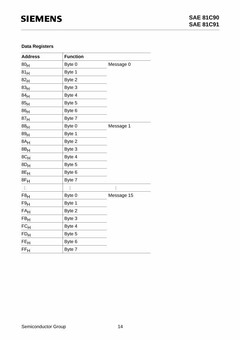
Data Registers
Address Function
80H Byte 0 Message 0
81H Byte 1
82H Byte 2
83H Byte 3
84H Byte 4
85H Byte 5
86H Byte 6
87H Byte 7
88H Byte 0 Message 1
89H Byte 1
8AH Byte 2
8BH Byte 3
8CH Byte 4
8DH Byte 5
8EH Byte 6
8FH Byte 7
: : :
F8H Byte 0 Message 15
F9H Byte 1
FAH Byte 2
FBH Byte 3
FCH Byte 4
FDH Byte 5
FEH Byte 6
FFH Byte 7
SAE 81C90SAE 81C91
Semiconductor Group 15
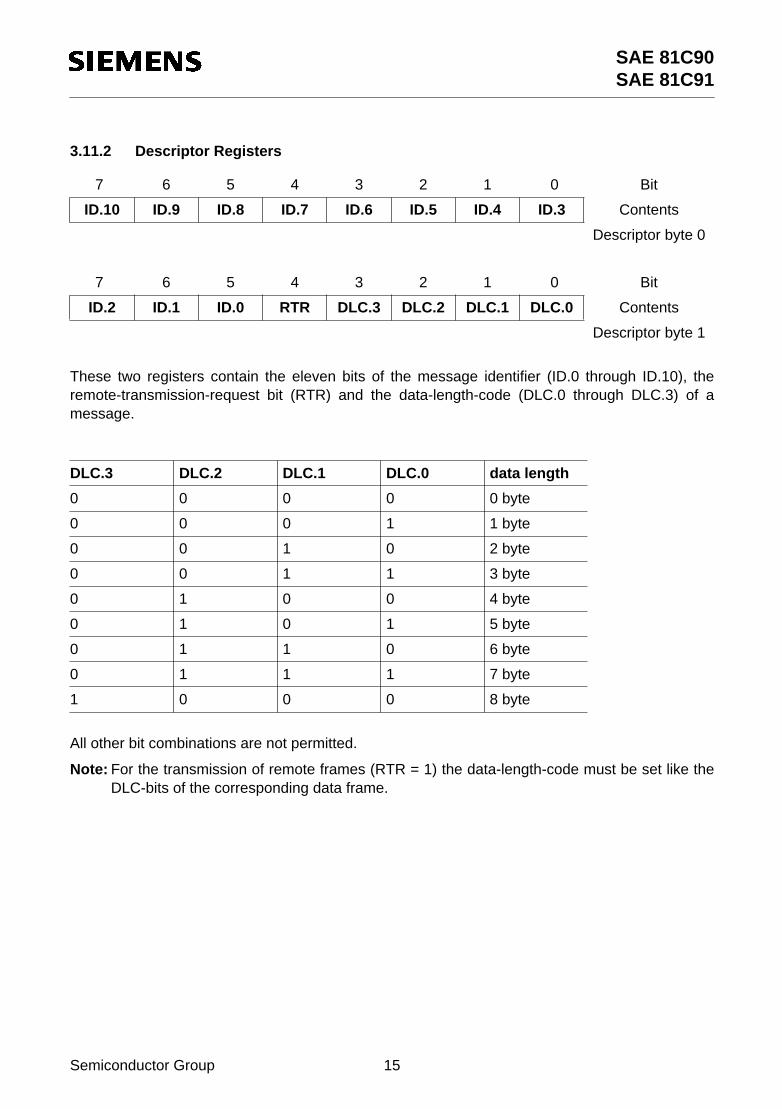
3.11.2 Descriptor Registers
These two registers contain the eleven bits of the message identifier (ID.0 through ID.10), theremote-transmission-request bit (RTR) and the data-length-code (DLC.0 through DLC.3) of amessage.
All other bit combinations are not permitted.
Note: For the transmission of remote frames (RTR = 1) the data-length-code must be set like theDLC-bits of the corresponding data frame.
7 6 5 4 3 2 1 0 Bit
ID.10 ID.9 ID.8 ID.7 ID.6 ID.5 ID.4 ID.3 Contents
Descriptor byte 0
7 6 5 4 3 2 1 0 Bit
ID.2 ID.1 ID.0 RTR DLC.3 DLC.2 DLC.1 DLC.0 Contents
Descriptor byte 1
DLC.3 DLC.2 DLC.1 DLC.0 data length
0 0 0 0 0 byte
0 0 0 1 1 byte
0 0 1 0 2 byte
0 0 1 1 3 byte
0 1 0 0 4 byte
0 1 0 1 5 byte
0 1 1 0 6 byte
0 1 1 1 7 byte
1 0 0 0 8 byte
SAE 81C90SAE 81C91
Semiconductor Group 16
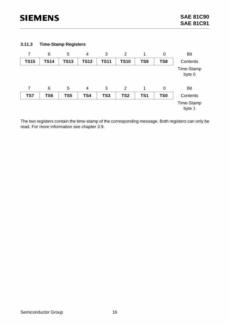
3.11.3 Time-Stamp Registers
The two registers contain the time-stamp of the corresponding message. Both registers can only beread. For more information see chapter 3.9.
7 6 5 4 3 2 1 0 Bit
TS15 TS14 TS13 TS12 TS11 TS10 TS9 TS8 Contents
Time-Stamp byte 0
7 6 5 4 3 2 1 0 Bit
TS7 TS6 TS5 TS4 TS3 TS2 TS1 TS0 Contents
Time-Stamp byte 1

SAE 81C90SAE 81C91
Semiconductor Group 17
3.11.4 Mode/Status-Register MOD
The register can be read and written except otherwise noted; the reset value is 00H.
7 6 5 4 3 2 1 0 Bit
ADE RS TC TWL RWL BS RES IM Contents
MOD
Symbol Position Function
IM MOD.0 Init ModeIM = 1: Setting this bit from 0 to 1 starts the initialisation mode:
– all bus activities are stopped– all registers are set to their reset value– access to read/write protected registers is enabledIf the bit stays set, the chip enters the normal mode, with enabled access to read/write protected registers.
IM = 0: Normal mode.
RES MOD.1 Reset RequestRES = 1: The chip enters the reset state:
– all bus activities are stopped– all registers are set to their reset value– the bus-off state is cancelled, if the bit is set for more than 1.5 x bit length
RES = 0: Normal mode
BS MOD.2 Bus State (read only)BS = 1: Bus-off state, the IC does not participate in bus activitiesBS = 0: Normal mode
RWL MOD.3 Receiver Warning Level (read only)RWL = 1: Receive-error counter larger or equal 96RWL = 0: Receive-error counter smaller 96
TWL MOD.4 Transmit Warning Level (read only)TWL = 1: Transmit-error counter larger or equal 96TWL = 0: Transmit-error counter smaller 96
TC MOD.5 Transmission Complete (read only)TC = 1: The last transmission request was executed successfullyTC = 0: The last transmission request was not executed successfully or
interrupted
RS MOD.6 Receive State (read only)RS = 1: Currently a message is receivedRS = 0: No receive
ADE MOD.7 Auto Decrement EnableADE = 1: With every read or write access using the serial synchronous
interface SI the address is decremented by one automatically. So one can access data continuously without the need of writing a new address
ADE = 0: No automatic address decrement
SAE 81C90SAE 81C91
Semiconductor Group 18
Notes on Bit TC
Scanning this bit is particularly useful if only one transmission is active. If there are severaltransmission jobs at the same time, it is better to scan the transmit-request register, because bit TCmay possibly only be set very briefly between acknowledgement of the previous message and thestart of the next one.
Notes on Bit RES and IM
There is a difference between a hardware reset (pin RES set to 0) and a software reset (bit RES setto 1). The bus-off state is cancelled immediately after a hardware reset. After a software reset thetime of 128 idle phases is waited, determined by the CAN protocol (1 idle phase = 11 recessive bitsin sequence).
The registers BL1, BL2, BRP and OC are set to 00H after a hardware reset or after both bits RESand IM are set to 1 (reset state of the chip).

SAE 81C90SAE 81C91
Semiconductor Group 19
3.11.5 Control Register CTRL
The register can be read and written; the reset value is 00H.
7 6 5 4 3 2 1 0 Bit
– TST TSP1 TSP0 TSOV SME TCE MM Contents
CTRL
Symbol Position Function
MM CTRL.0 Monitor ModeMM = 1: The memory location of message 0 receives all identifiers that
are not accepted by other memory locations (corresponds to a Basic CAN receive register).
MM = 0: The above memory location responds like all others.
TCE CTRL.1 Transmit Check EnableTCE = 1: If the transmit check detects an error, the message is
invalidated by an error frame and the error counter TCEC is incremented by 1. If the counter reaches 4, the bus-off status is initiated and, if enabled, an interrupt (TCI) is generated.
TCE = 0: If the transmit check detects an error, there is no intervention.
SME CTRL.2 Sleep Mode EnableSME = 1: The sleep mode is enabled: the crystal oscillator is deactivated,
all other activities are inhibited.The wake up is done also by a reset signal or by an active signal at the CS pin or by an input edge going from recessive to dominant at pin Rx0 respectively Rx1.
SME = 0: Normal operation.
TSOV CTRL.3 Time Stamp OverflowTSOV = 1:There was at least one overflow of the time-stamp timer.TSOV = 0:There has been no overflow.
TSP0TSP1
CTRL.4CTRL.5
Time Stamp PrescalerTSP1 TSP0 Clock of time-stamp timer0 0 fBL / 320 1 fBL / 641 0 fBL / 1281 1 fBL / 256For fBL see baud-rate prescaler BRP
TST CTRL.6 Time Stamp TestTST = 1: The time-stamp prescaler is deactivated. Only for test, bit IM
(MOD.0) must be set to 1.TST = 0: The prescaler is activated.
– CTRL.7 Reserved, must be 0.
SAE 81C90SAE 81C91
Semiconductor Group 20
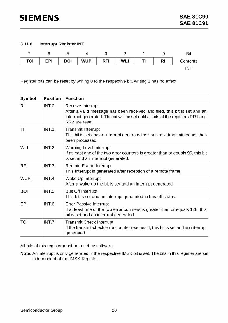
3.11.6 Interrupt Register INT
Register bits can be reset by writing 0 to the respective bit, writing 1 has no effect.
All bits of this register must be reset by software.
Note: An interrupt is only generated, if the respective IMSK bit is set. The bits in this register are setindependent of the IMSK-Register.
7 6 5 4 3 2 1 0 Bit
TCI EPI BOI WUPI RFI WLI TI RI Contents
INT
Symbol Position Function
RI INT.0 Receive InterruptAfter a valid message has been received and filed, this bit is set and aninterrupt generated. The bit will be set until all bits of the registers RR1 andRR2 are reset.
TI INT.1 Transmit InterruptThis bit is set and an interrupt generated as soon as a transmit request hasbeen processed.
WLI INT.2 Warning Level InterruptIf at least one of the two error counters is greater than or equals 96, this bitis set and an interrupt generated.
RFI INT.3 Remote Frame InterruptThis interrupt is generated after reception of a remote frame.
WUPI INT.4 Wake Up InterruptAfter a wake-up the bit is set and an interrupt generated.
BOI INT.5 Bus Off InterruptThis bit is set and an interrupt generated in bus-off status.
EPI INT.6 Error Passive InterruptIf at least one of the two error counters is greater than or equals 128, thisbit is set and an interrupt generated.
TCI INT.7 Transmit Check InterruptIf the transmit-check error counter reaches 4, this bit is set and an interruptgenerated.
SAE 81C90SAE 81C91
Semiconductor Group 21
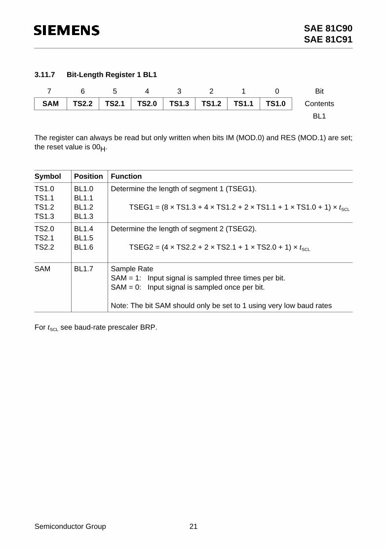
3.11.7 Bit-Length Register 1 BL1
The register can always be read but only written when bits IM (MOD.0) and RES (MOD.1) are set;the reset value is 00H.
For tSCL see baud-rate prescaler BRP.
7 6 5 4 3 2 1 0 Bit
SAM TS2.2 TS2.1 TS2.0 TS1.3 TS1.2 TS1.1 TS1.0 Contents
BL1
Symbol Position Function
TS1.0TS1.1TS1.2TS1.3
BL1.0BL1.1BL1.2BL1.3
Determine the length of segment 1 (TSEG1).
TSEG1 = (8 × TS1.3 + 4 × TS1.2 + 2 × TS1.1 + 1 × TS1.0 + 1) × tSCL
TS2.0TS2.1TS2.2
BL1.4BL1.5BL1.6
Determine the length of segment 2 (TSEG2).
TSEG2 = (4 × TS2.2 + 2 × TS2.1 + 1 × TS2.0 + 1) × tSCL
SAM BL1.7 Sample RateSAM = 1: Input signal is sampled three times per bit.SAM = 0: Input signal is sampled once per bit.
Note: The bit SAM should only be set to 1 using very low baud rates
SAE 81C90SAE 81C91
Semiconductor Group 22
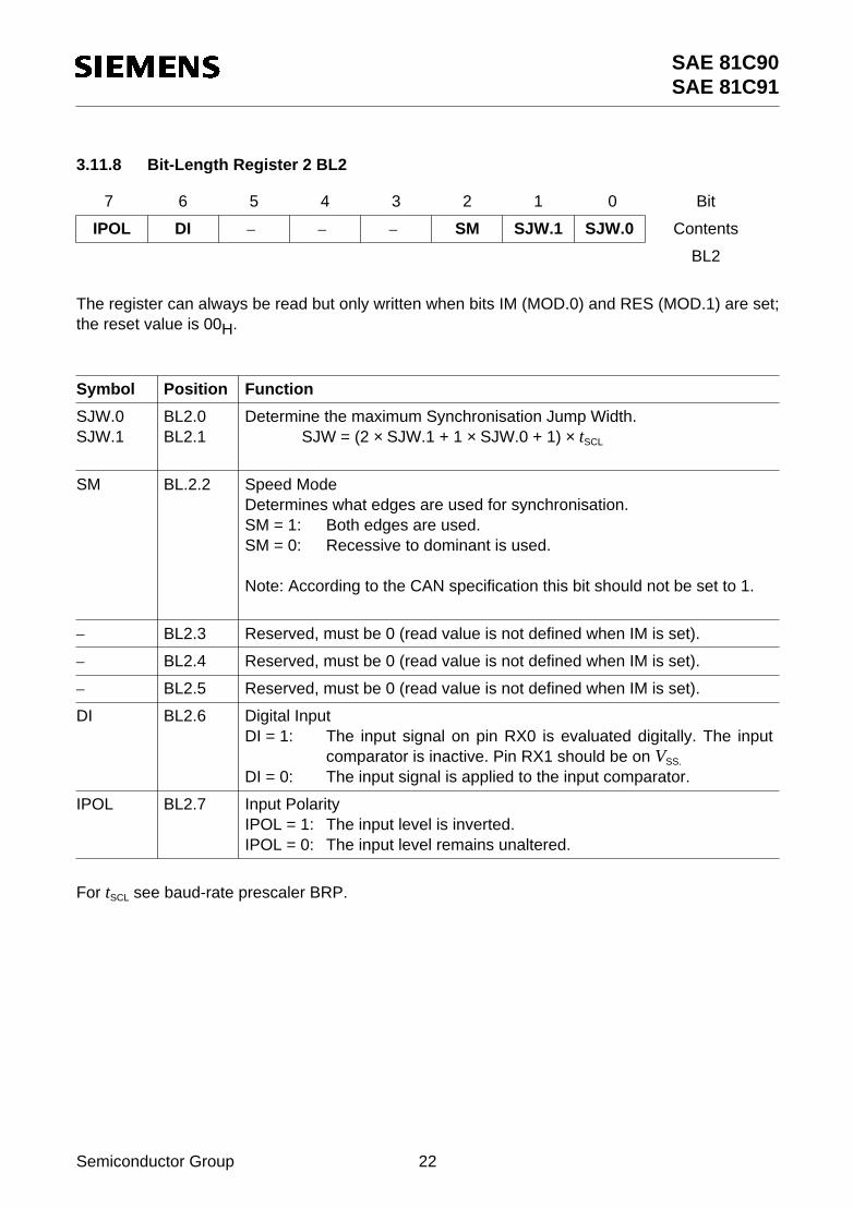
3.11.8 Bit-Length Register 2 BL2
The register can always be read but only written when bits IM (MOD.0) and RES (MOD.1) are set;the reset value is 00H.
For tSCL see baud-rate prescaler BRP.
7 6 5 4 3 2 1 0 Bit
IPOL DI – – – SM SJW.1 SJW.0 Contents
BL2
Symbol Position Function
SJW.0SJW.1
BL2.0BL2.1
Determine the maximum Synchronisation Jump Width.SJW = (2 × SJW.1 + 1 × SJW.0 + 1) × tSCL
SM BL.2.2 Speed ModeDetermines what edges are used for synchronisation.SM = 1: Both edges are used.SM = 0: Recessive to dominant is used.
Note: According to the CAN specification this bit should not be set to 1.
– BL2.3 Reserved, must be 0 (read value is not defined when IM is set).
– BL2.4 Reserved, must be 0 (read value is not defined when IM is set).
– BL2.5 Reserved, must be 0 (read value is not defined when IM is set).
DI BL2.6 Digital InputDI = 1: The input signal on pin RX0 is evaluated digitally. The input
comparator is inactive. Pin RX1 should be on VSS.
DI = 0: The input signal is applied to the input comparator.
IPOL BL2.7 Input PolarityIPOL = 1: The input level is inverted.IPOL = 0: The input level remains unaltered.
SAE 81C90SAE 81C91
Semiconductor Group 23
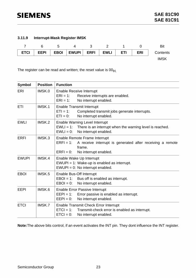
3.11.9 Interrupt-Mask Register IMSK
The register can be read and written; the reset value is 00H.
Note:The above bits control, if an event activates the INT pin. They dont influence the INT register.
7 6 5 4 3 2 1 0 Bit
ETCI EEPI EBOI EWUPI ERFI EWLI ETI ERI Contents
IMSK
Symbol Position Function
ERI IMSK.0 Enable Receive InterruptERI = 1: Receive interrupts are enabled.ERI = 1: No interrupt enabled.
ETI IMSK.1 Enable Transmit InterruptETI = 1: Completed transmit jobs generate interrupts.ETI = 0: No interrupt enabled.
EWLI IMSK.2 Enable Warning Level InterruptEWLI = 1: There is an interrupt when the warning level is reached.EWLI = 0: No interrupt enabled.
ERFI IMSK.3 Enable Remote Frame InterruptERFI = 1: A receive interrupt is generated after receiving a remote
frame.ERFI = 0: No interrupt enabled.
EWUPI IMSK.4 Enable Wake Up InterruptEWUPI = 1: Wake-up is enabled as interrupt.EWUPI = 0: No interrupt enabled.
EBOI IMSK.5 Enable Bus-Off InterruptEBOI = 1: Bus off is enabled as interrupt.EBOI = 0: No interrupt enabled.
EEPI IMSK.6 Enable Error Passive InterruptEEPI = 1: Error passive is enabled as interrupt.EEPI = 0: No interrupt enabled.
ETCI IMSK.7 Enable Transmit Check Error InterruptETCI = 1: Transmit-check error is enabled as interrupt.ETCI = 0: No interrupt enabled.

SAE 81C90SAE 81C91
Semiconductor Group 24
3.11.10 Baud Rate Prescaler BRP
The register is not readable and can only be written when bits IM (MOD.0) and RES (MOD.1) areset; the reset value is 00H.
tOSC = 1/quartz clock
The bit length tBL is computed as follows:
tBL = TSEG1 + TSEG2 + 1 tSCL
The baudrate BR is:
BR = fcrystal / (2 x (BRP + 1) x (TS1 + TS2 + 3))
Note:
BRP = BRP0..BRP5 see Baud Rate PrescalerTS1 = TS1.0..TS1.3 see Bit Length Register 1TS2 = TS2.0..TS2.2 see Bit Length Register 1
7 6 5 4 3 2 1 0 Bit
– – BRP5 BRP4 BRP3 BRP2 BRP1 BRP0 Contents
BRP
Symbol Position Function
BRP0BRP1BRP2BRP3BRP4BRP5
BRP.0BRP.1BRP.2BRP.3BRP.4BRP.5
Baud Rate PrescalerThis register determines the system clock
tSCL = (32 × BRP.5 + 16 × BRP.4 + 8 × BRP.3 + 4 × BRP.2 + 2 ×BRP.1 + 1 × BRP.0 + 1) × 2tOSC
– BRP.6 Reserved, must be 0
– BRP.7 Reserved, must be 0
SAE 81C90SAE 81C91
Semiconductor Group 25
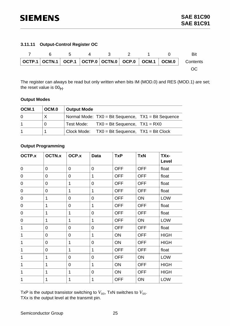
3.11.11 Output-Control Register OC
The register can always be read but only written when bits IM (MOD.0) and RES (MOD.1) are set;the reset value is 00H.
Output Modes
Output Programming
TxP is the output transistor switching to VDD, TxN switches to VSS.TXx is the output level at the transmit pin.
7 6 5 4 3 2 1 0 Bit
OCTP.1 OCTN.1 OCP.1 OCTP.0 OCTN.0 OCP.0 OCM.1 OCM.0 Contents
OC
OCM.1 OCM.0 Output Mode
0 X Normal Mode: TX0 = Bit Sequence, TX1 = Bit Sequence
1 0 Test Mode: TX0 = Bit Sequence, TX1 = RX0
1 1 Clock Mode: TX0 = Bit Sequence, TX1 = Bit Clock
OCTP.x OCTN.x OCP.x Data TxP TxN TXx-Level
0 0 0 0 OFF OFF float
0 0 0 1 OFF OFF float
0 0 1 0 OFF OFF float
0 0 1 1 OFF OFF float
0 1 0 0 OFF ON LOW
0 1 0 1 OFF OFF float
0 1 1 0 OFF OFF float
0 1 1 1 OFF ON LOW
1 0 0 0 OFF OFF float
1 0 0 1 ON OFF HIGH
1 0 1 0 ON OFF HIGH
1 0 1 1 OFF OFF float
1 1 0 0 OFF ON LOW
1 1 0 1 ON OFF HIGH
1 1 1 0 ON OFF HIGH
1 1 1 1 OFF ON LOW
SAE 81C90SAE 81C91
Semiconductor Group 26
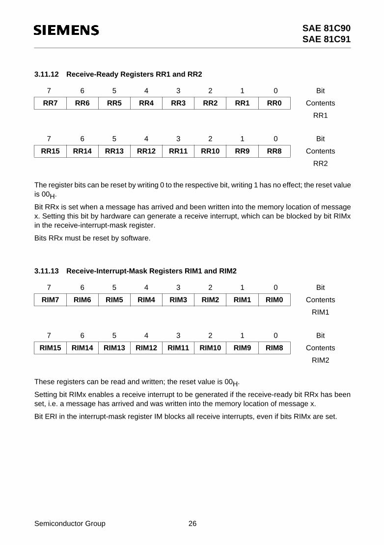
3.11.12 Receive-Ready Registers RR1 and RR2
The register bits can be reset by writing 0 to the respective bit, writing 1 has no effect; the reset valueis 00H.
Bit RRx is set when a message has arrived and been written into the memory location of messagex. Setting this bit by hardware can generate a receive interrupt, which can be blocked by bit RIMxin the receive-interrupt-mask register.
Bits RRx must be reset by software.
3.11.13 Receive-Interrupt-Mask Registers RIM1 and RIM2
These registers can be read and written; the reset value is 00H.
Setting bit RIMx enables a receive interrupt to be generated if the receive-ready bit RRx has beenset, i.e. a message has arrived and was written into the memory location of message x.
Bit ERI in the interrupt-mask register IM blocks all receive interrupts, even if bits RIMx are set.
7 6 5 4 3 2 1 0 Bit
RR7 RR6 RR5 RR4 RR3 RR2 RR1 RR0 Contents
RR1
7 6 5 4 3 2 1 0 Bit
RR15 RR14 RR13 RR12 RR11 RR10 RR9 RR8 Contents
RR2
7 6 5 4 3 2 1 0 Bit
RIM7 RIM6 RIM5 RIM4 RIM3 RIM2 RIM1 RIM0 Contents
RIM1
7 6 5 4 3 2 1 0 Bit
RIM15 RIM14 RIM13 RIM12 RIM11 RIM10 RIM9 RIM8 Contents
RIM2

SAE 81C90SAE 81C91
Semiconductor Group 27
3.11.14 Transmit-Request Registers TR1 and TR2
The transmit-request registers are each divided in the addresses for setting and resetting of thetransmission request. In this manner it is prevented that when writing these registers bits becomeset again which meanwhile were reset because of a completed transmission.
3.11.14.1 Transmit-Request-Set Registers TRS1 and TRS2
These registers can be read. Writing 1 to a bit takes effect, writing 0 has no effect; the reset valueis 00H.
Setting bit TRx causes the particular message x to be transmitted. The bit is reset by hardware aftertransmission. Several bits can be set simultaneously. In this way all messages whose request bitsare set are transmitted in turn, starting with the memory location with the highest number.
3.11.14.2 Transmit-Request-Reset Registers TRR1 and TRR2
These registers can not be read and only writing 1 to a bit takes effect.
Setting bit TRRx causes a transmission request, initiated by the corresponding bit TRSx, to becancelled, provided that it is not currently processed. Bit TRSx is set to 0 by this action.
7 6 5 4 3 2 1 0 Bit
TRS7 TRS6 TRS5 TRS4 TRS3 TRS2 TRS1 TRS0 Contents
TRS1
7 6 5 4 3 2 1 0 Bit
TRS15 TRS14 TRS13 TRS12 TRS11 TRS10 TRS9 TRS8 Contents
TRS2
7 6 5 4 3 2 1 0 Bit
TRR7 TRR6 TRR5 TRR4 TRR3 TRR2 TRR1 TRR0 Contents
TRR1
7 6 5 4 3 2 1 0 Bit
TRR15 TRR14 TRR13 TRR12 TRR11 TRR10 TRR9 TRR8 Contents
TRR2
SAE 81C90SAE 81C91
Semiconductor Group 28
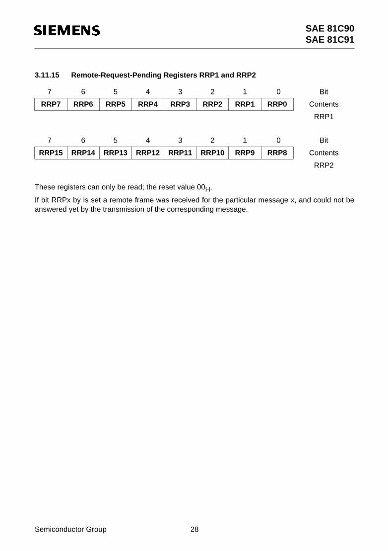
3.11.15 Remote-Request-Pending Registers RRP1 and RRP2
These registers can only be read; the reset value 00H.
If bit RRPx by is set a remote frame was received for the particular message x, and could not beanswered yet by the transmission of the corresponding message.
7 6 5 4 3 2 1 0 Bit
RRP7 RRP6 RRP5 RRP4 RRP3 RRP2 RRP1 RRP0 Contents
RRP1
7 6 5 4 3 2 1 0 Bit
RRP15 RRP14 RRP13 RRP12 RRP11 RRP10 RRP9 RRP8 Contents
RRP2

SAE 81C90SAE 81C91
Semiconductor Group 29
3.11.16 Port Register
Port-Latch Registers
Port-Pin Registers
Port-Direction Registers
Except the port-pin registers, which can only be read, all registers can be read and written; the resetvalue of the port registers is 00H.
After a reset, the ports are switched as inputs. The state of the pin can be read via the port register.Setting a bit of the port-direction register to 1 causes the associated port pin to be switched as anoutput. The output data can then be written (latched) into the port register. The latch can be readfrom the port-latch register, the levels on the port pins from the port-pin register,
In parallel to the standard CMOS structure there is an additional internal pull up resistor of about250 kΩ at each port pin.
7 6 5 4 3 2 1 0 Bit
D7 D6 D5 D4 D3 D2 D1 D0 Contents
P0LR, P1LR
7 6 5 4 3 2 1 0 Bit
D7 D6 D5 D4 D3 D2 D1 D0 Contents
P0PR, P1PR
7 6 5 4 3 2 1 0 Bit
D7 D6 D5 D4 D3 D2 D1 D0 Contents
P0PDR, P1PDR

SAE 81C90SAE 81C91
Semiconductor Group 30
3.11.17 Clock-Control Register CC
This register can only be written; the reset value is 01H.
This register determines the output freuency at pin CLK.
Bits 4 through 7 must be 0.
7 6 5 4 3 2 1 0 Bit
– – – – CC3 CC2 CC1 CC0 Contents
CC
CC3 CC2 CC1 CC0 output frequency
0 0 0 0 fOSC
0 0 0 1 fOSC/2
0 0 1 0 fOSC/4
0 0 1 1 fOSC/6
0 1 0 0 fOSC/8
0 1 0 1 fOSC/10
0 1 1 0 fOSC/12
0 1 1 1 fOSC/14
1 X X X switched off (Low level)
SAE 81C90SAE 81C91
Semiconductor Group 31
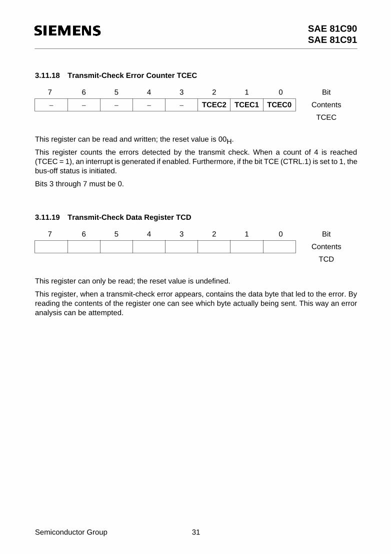
3.11.18 Transmit-Check Error Counter TCEC
This register can be read and written; the reset value is 00H.
This register counts the errors detected by the transmit check. When a count of 4 is reached(TCEC = 1), an interrupt is generated if enabled. Furthermore, if the bit TCE (CTRL.1) is set to 1, thebus-off status is initiated.
Bits 3 through 7 must be 0.
3.11.19 Transmit-Check Data Register TCD
This register can only be read; the reset value is undefined.
This register, when a transmit-check error appears, contains the data byte that led to the error. Byreading the contents of the register one can see which byte actually being sent. This way an erroranalysis can be attempted.
7 6 5 4 3 2 1 0 Bit
– – – – – TCEC2 TCEC1 TCEC0 Contents
TCEC
7 6 5 4 3 2 1 0 Bit
Contents
TCD
SAE 81C90SAE 81C91
Semiconductor Group 32
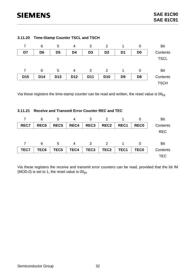
3.11.20 Time-Stamp Counter TSCL and TSCH
Via these registers the time-stamp counter can be read and written, the reset value is 00H.
3.11.21 Receive and Transmit Error Counter REC and TEC
Via these registers the receive and transmit error counters can be read, provided that the bit IM(MOD.0) is set to 1, the reset value is 00H.
7 6 5 4 3 2 1 0 Bit
D7 D6 D5 D4 D3 D2 D1 D0 Contents
TSCL
7 6 5 4 3 2 1 0 Bit
D15 D14 D13 D12 D11 D10 D9 D8 Contents
TSCH
7 6 5 4 3 2 1 0 Bit
REC7 REC6 REC5 REC4 REC3 REC2 REC1 REC0 Contents
REC
7 6 5 4 3 2 1 0 Bit
TEC7 TEC6 TEC5 TEC4 TEC3 TEC2 TEC1 TEC0 Contents
TEC
SAE 81C90SAE 81C91
Semiconductor Group 33
4 Communication and Protocol
Details of this item will be added later. But the following points should be dealt with.
4.1 Bit Timing
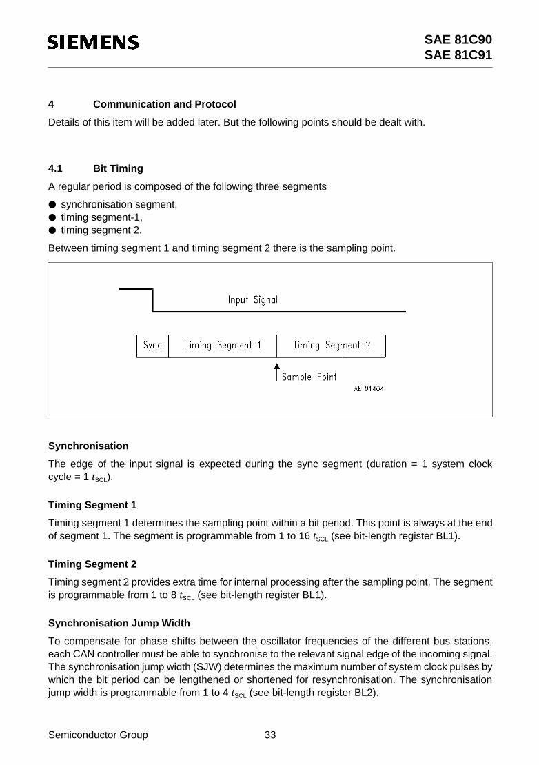
A regular period is composed of the following three segments
synchronisation segment, timing segment-1, timing segment 2.
Between timing segment 1 and timing segment 2 there is the sampling point.
Synchronisation
The edge of the input signal is expected during the sync segment (duration = 1 system clockcycle = 1 tSCL).
Timing Segment 1
Timing segment 1 determines the sampling point within a bit period. This point is always at the endof segment 1. The segment is programmable from 1 to 16 tSCL (see bit-length register BL1).
Timing Segment 2
Timing segment 2 provides extra time for internal processing after the sampling point. The segmentis programmable from 1 to 8 tSCL (see bit-length register BL1).
Synchronisation Jump Width
To compensate for phase shifts between the oscillator frequencies of the different bus stations,each CAN controller must be able to synchronise to the relevant signal edge of the incoming signal.The synchronisation jump width (SJW) determines the maximum number of system clock pulses bywhich the bit period can be lengthened or shortened for resynchronisation. The synchronisationjump width is programmable from 1 to 4 tSCL (see bit-length register BL2).

SAE 81C90SAE 81C91
Semiconductor Group 34
Example of Lengthening Bit Period:
Example of Shortening Bit Period:
Delay Times
The total delay is calculated from the following single delays:
2 × physical bus tBus (max. 100 ns acc. to CAN specification), 2 × input comporator tComp (depends on application circuit), 2 × output driver tDriver (depends on application circuit), 1 × input to output of CAN controller tInOut (max. 1 tSCL + 80 ns)
tDelay = 2 × (tBus + tComp + tDriver) + tInOut
Recommendations
On the basis of the stated conditions, there are the following essential requirements to bemaintained:
tTSEG1 ≥ tSEG2
tTSEG1 ≥ tDelay
tTSEG2 > tSJW
tTSEG1 = 2 × tTSEG2
if bit SAM = 1 then TSEG2 ≥ 3 x tSCL + SJW
SAE 81C90SAE 81C91
Semiconductor Group 35
5 Host Interfaces
There are two different host interfaces implemented in the SAE 81C90 / SAE 81C91.
Data and addresses on a multiplexed 8-bit bus, compatible with Siemens microcontrollers(SAB 80C5xx, SAB 80C16x), can be transferred via the parallel interface (PI). Using the serialsynchronous interface (Sl), any host controller with a serial three-lead interface can be connectedwith.
The interface is selected by hardware through the wiring of the MS (Mode Select) pin. This pin maynot be switched during operation. If there is a High level on the MS pin, the SI and thus pins DI, DO,CLK, W and TIM are activated, while pins AD5 through AD7, RD, WR and ALE are inactive. A Lowlevel on the MS pin switches to the Pl and thus activates pins AD0 through AD7, RD, WR and ALE.
5.1 Parallel Interface Pl
The parallel interface consists of a multiplexed 8-bit address/data bus. First the address of therequired register is applied to the pins AD0 through AD7. A falling edge on pin ALE means that thisaddress is transferred to an on-chip latch. After this, data can either be written into the selectedregister (pin WR = 0) or read from it (pin RD = 0) on the address/data bus. Pin CS must be 0 for theentire duration of the RD/WR active time so that the circuit is activated.
5.2 Serial Synchronous Interface Sl
If the SI is used, the unused pins of the PI must be set to inactive levels (RD, WR to VDD and ALE,AD5, AD6, AD7 to VSS).
Communication on the SI is according to the following procedure:
Each access to the stand-alone Full-CAN circuit has to be started by activating the device (CS = 0).After the beginning of access, an address must be written first and then data can be read or written.The required function is determined by pin W (W = 1: read; W = 0: write). If the automaticdecrementing of the address is activated (bit ADE in the MOD register), any number of data bytescan be accessed in succession. Finally the device has to be deactivated.
Procedure:
Activate device (CS = 0) Set pin W to 1 for read, to 0 for write Write in address of first data byte Read out/write in one or more data bytes Deactivate device (CS = 1)
SAE 81C90SAE 81C91
Semiconductor Group 36
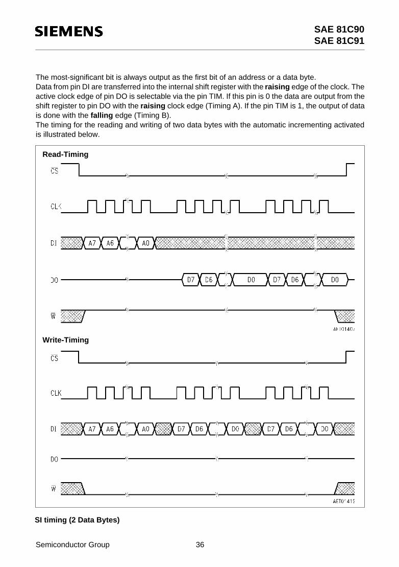
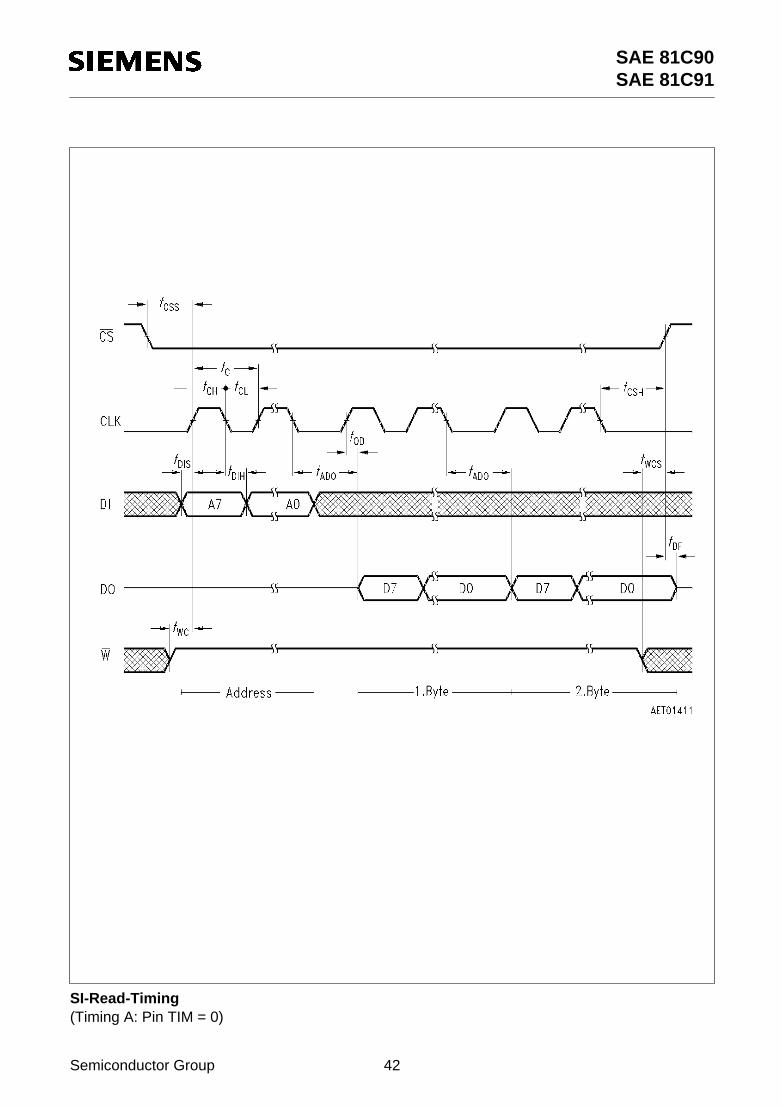
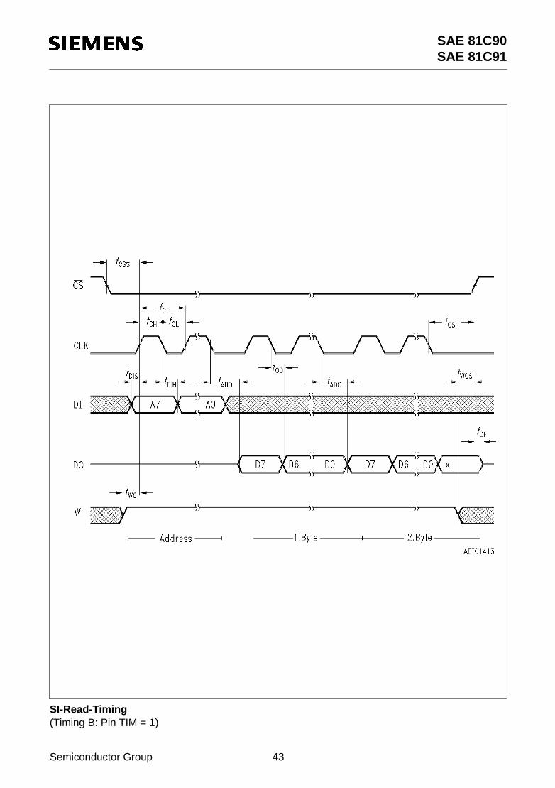
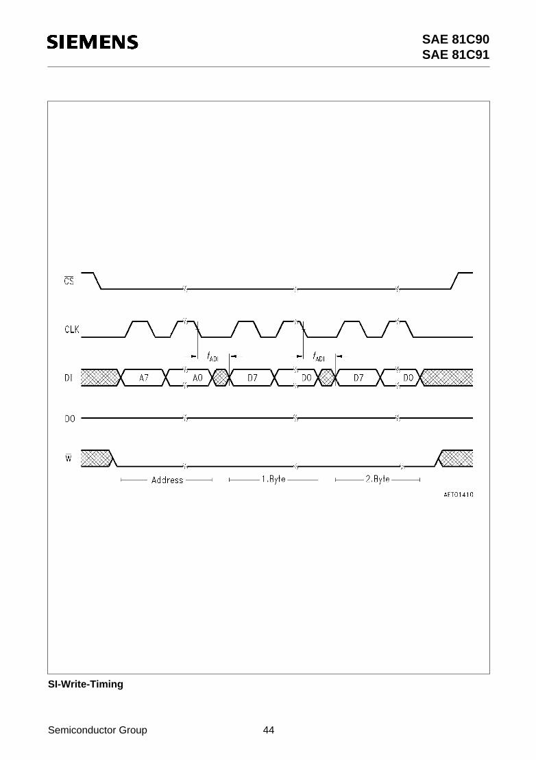
The most-significant bit is always output as the first bit of an address or a data byte.Data from pin DI are transferred into the internal shift register with the raising edge of the clock. Theactive clock edge of pin DO is selectable via the pin TIM. If this pin is 0 the data are output from theshift register to pin DO with the raising clock edge (Timing A). If the pin TIM is 1, the output of datais done with the falling edge (Timing B).The timing for the reading and writing of two data bytes with the automatic incrementing activatedis illustrated below.
Read-Timing
Write-Timing
SI timing (2 Data Bytes)
SAE 81C90SAE 81C91
Semiconductor Group 37
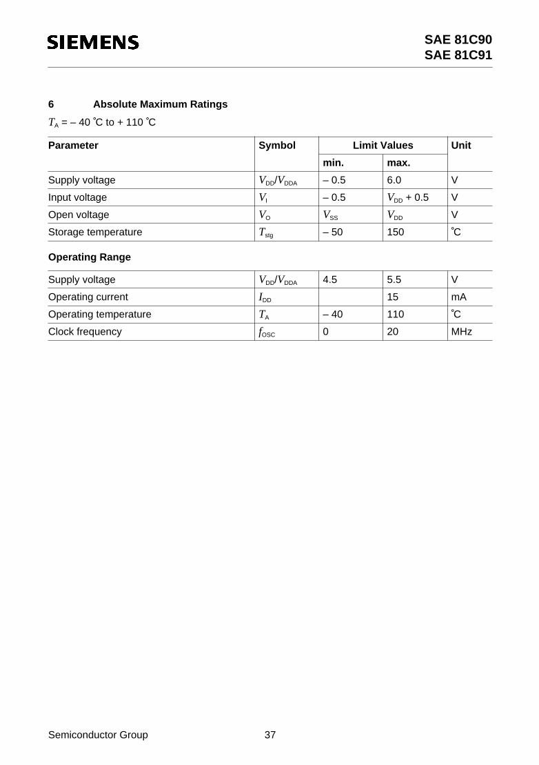
6 Absolute Maximum Ratings
TA = – 40 ˚C to + 110 ˚C
Parameter Symbol Limit Values Unit
min. max.
Supply voltage VDD/VDDA – 0.5 6.0 V
Input voltage VI – 0.5 VDD + 0.5 V
Open voltage VO VSS VDD V
Storage temperature Tstg – 50 150 ˚C
Operating Range
Supply voltage VDD/VDDA 4.5 5.5 V
Operating current IDD 15 mA
Operating temperature TA – 40 110 ˚C
Clock frequency fOSC 0 20 MHz
SAE 81C90SAE 81C91
Semiconductor Group 38
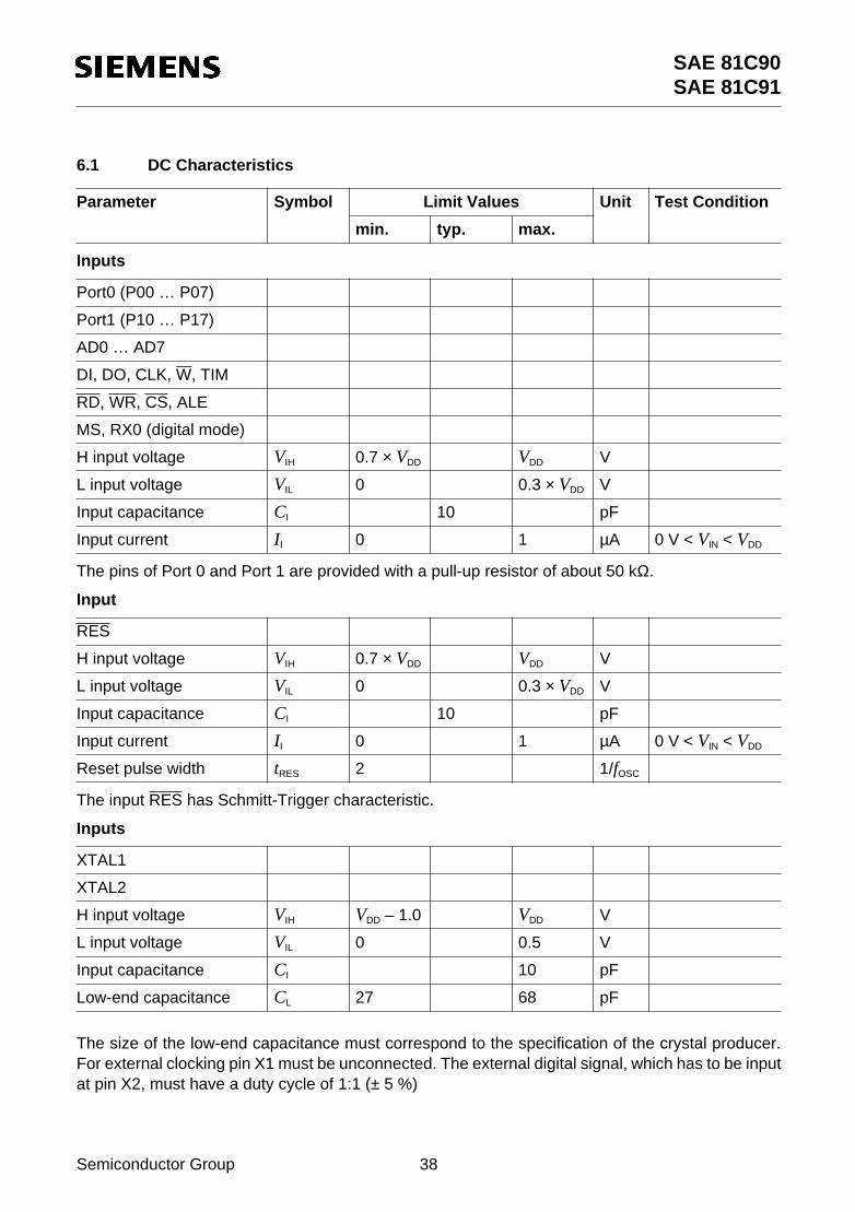
6.1 DC Characteristics
The size of the low-end capacitance must correspond to the specification of the crystal producer.For external clocking pin X1 must be unconnected. The external digital signal, which has to be inputat pin X2, must have a duty cycle of 1:1 (± 5 %)
Parameter Symbol Limit Values Unit Test Condition
min. typ. max.
Inputs
Port0 (P00 … P07)
Port1 (P10 … P17)
AD0 … AD7
DI, DO, CLK, W, TIM
RD, WR, CS, ALE
MS, RX0 (digital mode)
H input voltage VIH 0.7 × VDD VDD V
L input voltage VIL 0 0.3 × VDD V
Input capacitance CI 10 pF
Input current II 0 1 µA 0 V < VIN < VDD
The pins of Port 0 and Port 1 are provided with a pull-up resistor of about 50 kΩ.
Input
RES
H input voltage VIH 0.7 × VDD VDD V
L input voltage VIL 0 0.3 × VDD V
Input capacitance CI 10 pF
Input current II 0 1 µA 0 V < VIN < VDD
Reset pulse width tRES 2 1/fOSC
The input RES has Schmitt-Trigger characteristic.
Inputs
XTAL1
XTAL2
H input voltage VIH VDD – 1.0 VDD V
L input voltage VIL 0 0.5 V
Input capacitance CI 10 pF
Low-end capacitance CL 27 68 pF

SAE 81C90SAE 81C91
Semiconductor Group 39
DC Characteristics (cont’d)
*) are not tested
Parameter Symbol Limit Values Unit Test Condition
min. typ. max.
Comparator Inputs
RX0, RX1
Input voltage VI 0.5 VDD + 0.5 V
Common mode voltage*) VICOM 1.5 VDD – 1.5 V
Input capacitance*) CI 10 pF
Input current IL 1 µA
Hysteresis*) VHYS 100 mV
Offset voltage*) VOff 100 mV
Note: If the bus lines work according to the ISO specification, additional circuitry is necessary forinterconnection of the input comparator to the bus lines.
Outputs
Port0 (P00 … P07)
Port1 (P10 … P17)
AD0 … AD7
INT
H output voltage VOH 0.8 × VDD VDD V IOH = 1.6 mA
L output voltage VOL 0 0.2 × VDD V IOL = 1.6 mA
Rise time*) tQR 40 ns CL = 30 pF
Fall time*) tQF 40 ns CL = 30 pF
Output
CLKOUT
H output voltage VOH 0.8 × VDD VDD V IOH = 10 mA
L output voltage VOL 0 0.4 V IOL = 10 mA
Rise time*) tQR 20 ns CL = 50 pF
Fall time*) tQF 20 ns CL = 50 pF
Driver Outputs
TX0, TX1
Source output current ISRC 5 mA VO = 0.8 × VDD
Sink output current ISNK 5 mA VO = 0.2 × VDD
SAE 81C90SAE 81C91
Semiconductor Group 40
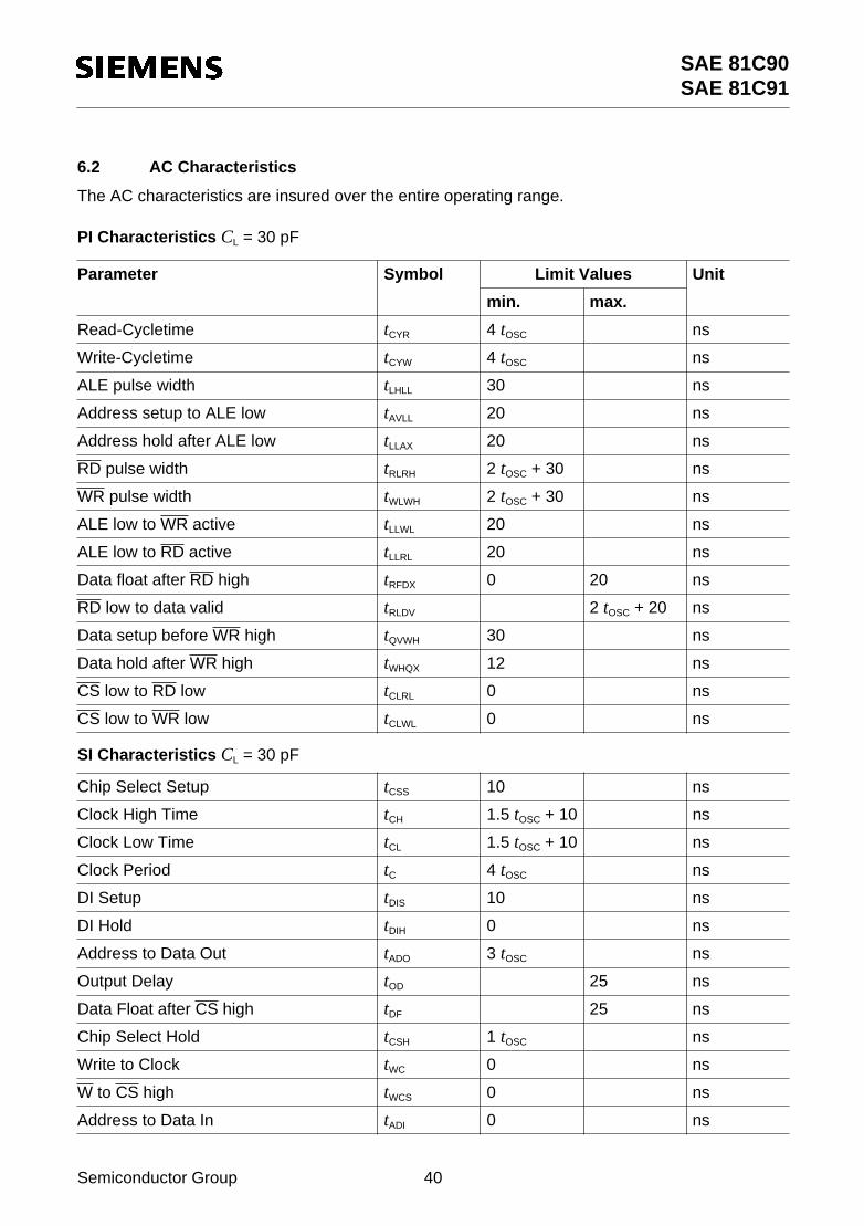
6.2 AC Characteristics
The AC characteristics are insured over the entire operating range.
PI Characteristics CL = 30 pF
Parameter Symbol Limit Values Unit
min. max.
Read-Cycletime tCYR 4 tOSC ns
Write-Cycletime tCYW 4 tOSC ns
ALE pulse width tLHLL 30 ns
Address setup to ALE low tAVLL 20 ns
Address hold after ALE low tLLAX 20 ns
RD pulse width tRLRH 2 tOSC + 30 ns
WR pulse width tWLWH 2 tOSC + 30 ns
ALE low to WR active tLLWL 20 ns
ALE low to RD active tLLRL 20 ns
Data float after RD high tRFDX 0 20 ns
RD low to data valid tRLDV 2 tOSC + 20 ns
Data setup before WR high tQVWH 30 ns
Data hold after WR high tWHQX 12 ns
CS low to RD low tCLRL 0 ns
CS low to WR low tCLWL 0 ns
SI Characteristics CL = 30 pF
Chip Select Setup tCSS 10 ns
Clock High Time tCH 1.5 tOSC + 10 ns
Clock Low Time tCL 1.5 tOSC + 10 ns
Clock Period tC 4 tOSC ns
DI Setup tDIS 10 ns
DI Hold tDIH 0 ns
Address to Data Out tADO 3 tOSC ns
Output Delay tOD 25 ns
Data Float after CS high tDF 25 ns
Chip Select Hold tCSH 1 tOSC ns
Write to Clock tWC 0 ns
W to CS high tWCS 0 ns
Address to Data In tADI 0 ns
SAE 81C90SAE 81C91
Semiconductor Group 41
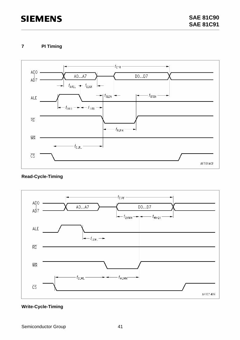
7 PI Timing
Read-Cycle-Timing
Write-Cycle-Timing
SAE 81C90SAE 81C91
Semiconductor Group 42
SI-Read-Timing(Timing A: Pin TIM = 0)
SAE 81C90SAE 81C91
Semiconductor Group 43
SI-Read-Timing(Timing B: Pin TIM = 1)
SAE 81C90SAE 81C91
Semiconductor Group 44
SI-Write-Timing
SAE 81C90SAE 81C91
Semiconductor Group 45
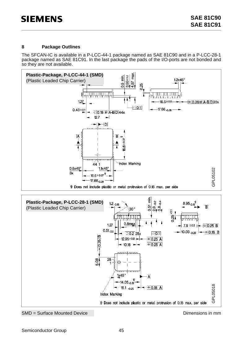
8 Package Outlines
The SFCAN-IC is available in a P-LCC-44-1 package named as SAE 81C90 and in a P-LCC-28-1package named as SAE 81C91. In the last package the pads of the I/O-ports are not bonded andso they are not available.
SMD = Surface Mounted Device Dimensions in mm
Plastic-Package, P-LCC-44-1 (SMD)(Plastic Leaded Chip Carrier)
GP
L051
02
Plastic-Package, P-LCC-28-1 (SMD)(Plastic Leaded Chip Carrier)
GP
L050
18