Embed Size (px)
Citation preview
Product Specification
1 / 28
LC320EXN
Ver. 1.1
FOR
APPROVAL
SPECIFICATION
Title 32.0” WXGA TFT LCD
BUYER General
MODEL
SUPPLIER LG Display Co., Ltd.
*MODEL LC320EXN
SUFFIX SCA1
*When you obtain standard approval,
please use the above model name without suffix
)
)
(
(
Final Specification
Preliminary Specification
APPROVED BYSIGNATURE
DATE
/
/
/
Please return 1 copy for your confirmation with
your signature and comments.
SIGNATURE
DATE
H.S.SONG / Team Leader
Y.J.KIM / Project Leader
Y.C.JANG / Engineer
TV Product Development Dept.
LG Display Co., Ltd
REVIEWED BY
PREPARED BY
APPROVED BY
Product Specification
2 / 28
LC320EXN
Ver. 1.1
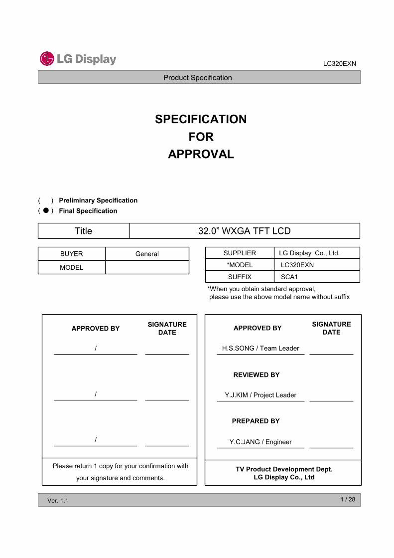
CONTENTS
24EMC7-2
24Environment7-3
Number ITEM Page
COVER 1
CONTENTS 2
RECORD OF REVISIONS 3
1 GENERAL DESCRIPTION 4
2 ABSOLUTE MAXIMUM RATINGS 5
3 ELECTRICAL SPECIFICATIONS 6
3-1 ELECTRICAL CHARACTERISTICS 6
3-2 INTERFACE CONNECTIONS 8
3-3 SIGNAL TIMING SPECIFICATIONS 10
3-4 LVDS SIGNAL SPECIFICATIONS 12
3-5 COLOR DATA REFERENCE 13
3-6 POWER SEQUENCE 14
4 OPTICAL SPECIFICATIONS 16
5 MECHANICAL CHARACTERISTICS 20
6 RELIABILITY 23
7 INTERNATIONAL STANDARDS 24
7-1 SAFETY 24
8 PACKING 25
8-1 DESIGNATION OF LOT MARK 25
8-2 PACKING FORM 25
9 PRECAUTIONS 26
9-1 MOUNTING PRECAUTIONS 26
9-2 OPERATING PRECAUTIONS 26
9-3 ELECTROSTATIC DISCHARGE CONTROL 27
9-4 PRECAUTIONS FOR STRONG LIGHT EXPOSURE 27
9-5 STORAGE 27
9-6 HANDLING PRECAUTIONS FOR PROTECTION FILM 27
Product Specification
3 / 28
LC320EXN
Ver. 1.1
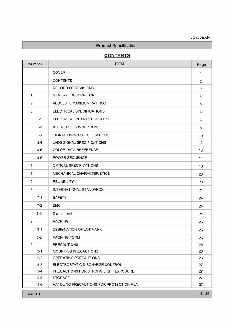
Changed Safty standard25May. 27, 20101.0
Update LCM Drawing22,23Aug. 19, 20101.1
Final Specification-
Revision No. Revision Date Page Description
0.0 Apr. 27, 2010 - Preliminary Specification (First Draft)
RECORD OF REVISIONS
Product Specification
4 / 28
LC320EXN
Ver. 1.1
General Features
Active Screen Size 31.51 inches(800.4mm) diagonal
Outline Dimension 741.4 mm(H) x 435.8 mm(V) x 23.6 mm(D) (Typ.)
Pixel Pitch 510.75 x 170.25 x RGB
Pixel Format 1366 horiz. by 768 vert. pixels RGB stripe arrangement
Color Depth 8bit, 16,7 M colors
Luminance, White 400 cd/m2 (Center 1 point) (Typ.)
Viewing Angle (CR>10) Viewing angle free ( R/L 178(Min.), U/D 178(Min.))
Power Consumption Total 45.44 Watt (Logic=4.2 W , LED Driver = 41.9W @ [ExtVbr_B=100%] )
Weight 5,900g(Typ.)
Display Operating Mode Transmissive mode, normally black
Surface Treatment Hard coating(3H), Anti-glare treatment of the front polarizer (Haze 10%)
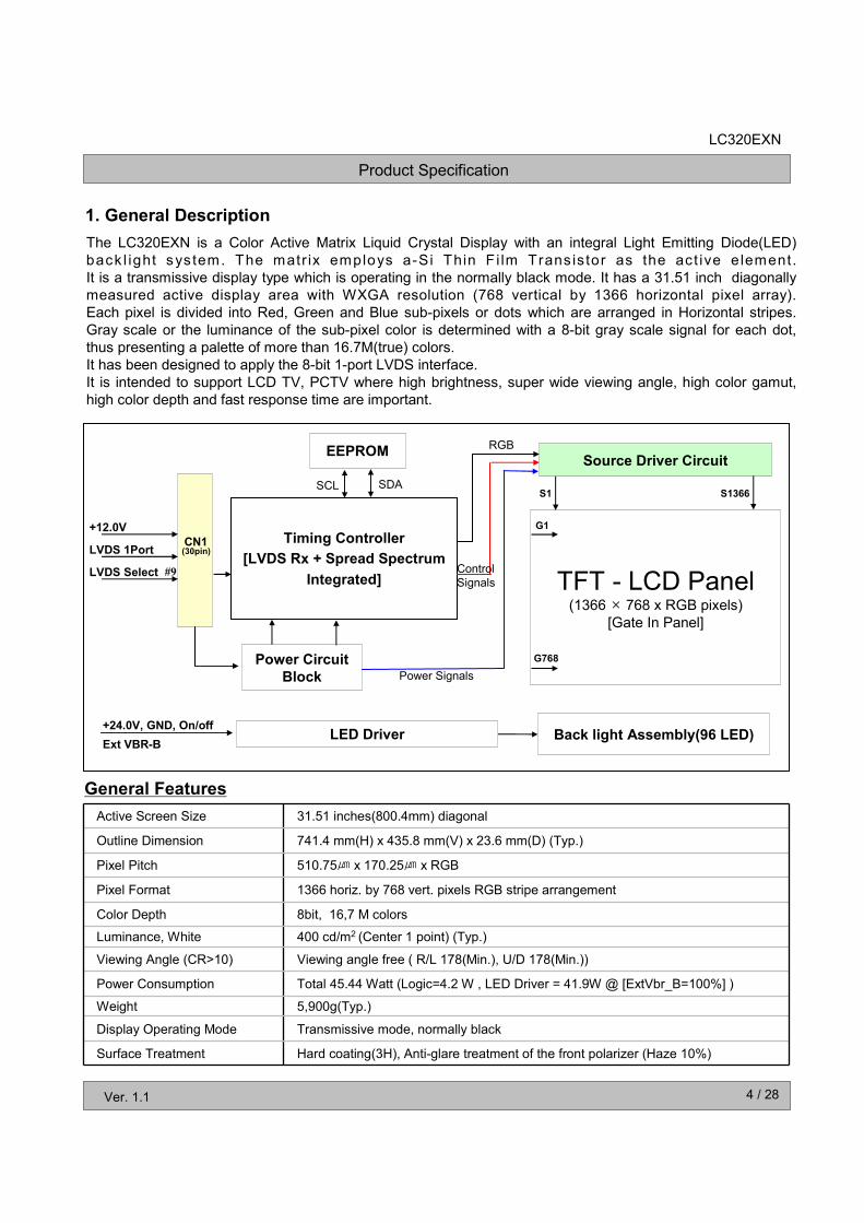
1. General Description
The LC320EXN is a Color Active Matrix Liquid Crystal Display with an integral Light Emitting Diode(LED)
back l ight sys tem. The matr ix employs a-Si Thin F i lm Trans istor as the act ive e lement.
It is a transmissive display type which is operating in the normally black mode. It has a 31.51 inch diagonally
measured active display area with WXGA resolution (768 vertical by 1366 horizontal pixel array).
Each pixel is divided into Red, Green and Blue sub-pixels or dots which are arranged in Horizontal stripes.
Gray scale or the luminance of the sub-pixel color is determined with a 8-bit gray scale signal for each dot,
thus presenting a palette of more than 16.7M(true) colors.
It has been designed to apply the 8-bit 1-port LVDS interface.
It is intended to support LCD TV, PCTV where high brightness, super wide viewing angle, high color gamut,
high color depth and fast response time are important.
CN1(30pin)
Power Circuit
Block
Source Driver Circuit
S1 S1366
RGB
TFT - LCD Panel(1366 × 768 x RGB pixels)
[Gate In Panel]
Timing Controller
[LVDS Rx + Spread Spectrum
Integrated]
EEPROM
SDASCL
LVDS 1Port
+12.0V
LVDS Select #9
Back light Assembly(96 LED)Ext VBR-B
LED Driver+24.0V, GND, On/off
Control
Signals
Power Signals
G1
G768
Product Specification
5 / 28
LC320EXN
Ver. 1.1
The following items are maximum values which, if exceeded, may cause faulty operation or damage to the
LCD module.
Table 1. ABSOLUTE MAXIMUM RATINGS
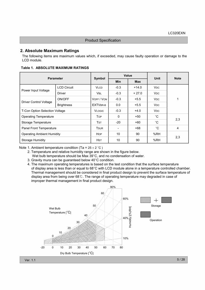
2. Absolute Maximum Ratings
90%
10 20 30 40 50 60 70 800-20
0
10
20
30
40
50
Dry Bulb Temperature [°C]
Wet Bulb
Temperature [°C]
Storage
Operation
Humidity [(%)RH]
10%
40%
60%
60
1. Ambient temperature condition (Ta = 25 ± 2 °C )
2. Temperature and relative humidity range are shown in the figure below.
Wet bulb temperature should be Max 39°C, and no condensation of water. 3. Gravity mura can be guaranteed below 40°C condition.4. The maximum operating temperatures is based on the test condition that the surface temperature
of display area is less than or equal to 68°C with LCD module alone in a temperature controlled chamber.Thermal management should be considered in final product design to prevent the surface temperature of
display area from being over 68. The range of operating temperature may degraded in case ofimproper thermal management in final product design.
VDC+ 27.0-0.3VBLDriver
VDC+14.0-0.3VLCDLCD CircuitPower Input Voltage
2,3°C+500TOPOperating Temperature
2,3
4
%RH9010HOPOperating Ambient Humidity
Brightness
VDC+4.0-0.3VLOGICT-Con Option Selection Voltage
ON/OFF
Unit
°C+68-TSURPanel Front Temperature
%RH9010HSTStorage Humidity
°C+60-20TSTStorage Temperature
1
VDC+5.50.0EXTVBR-B
VDC+5.5-0.3VOFF / VONDriver Control Voltage
MaxMinParameter Note
ValueSymbol
Note
Product Specification
6 / 28
LC320EXN
Ver. 1.1
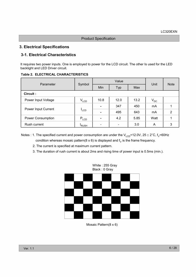
Table 2. ELECTRICAL CHARACTERISTICS
Notes : 1. The specified current and power consumption are under the VLCD=12.0V, 25 ± 2°C, fV=60Hz
condition whereas mosaic pattern(8 x 6) is displayed and fV is the frame frequency.
2. The current is specified at maximum current pattern.
3. The duration of rush current is about 2ms and rising time of power input is 0.5ms (min.).
Parameter SymbolValue
Unit NoteMin Typ Max
Circuit :
Power Input Voltage VLCD 10.8 12.0 13.2 VDC
Power Input Current ILCD
- 347 450 mA 1
- 495 643 mA 2
Power Consumption PLCD - 4.2 5.85 Watt 1
Rush current IRUSH - - 3.0 A 3
3. Electrical Specifications
3-1. Electrical Characteristics
Mosaic Pattern(8 x 6)
White : 255 Gray
Black : 0 Gray
It requires two power inputs. One is employed to power for the LCD circuit. The other Is used for the LED
backlight and LED Driver circuit.
Product Specification
7 / 28
LC320EXN
Ver. 1.1 7 / 28
Table 3. ELECTRICAL CHARACTERISTICS (Continue)
Parameter SymbolValues
Unit NotesMin Typ Max
LED Driver :
Power Supply Input Voltage VBL 22.8 24.0 25.2 Vdc 1
Power Supply Input Current IBL_A - 1.7 1.8 A 1
Power Supply Input Current (In-Rush) Irush - - 2.5 AVBL = 22.8V
Ext VBR-B = 100%
Power Consumption PBL - 41.9 44.5 W 1
Input Voltage for Control System Signals
On/OffOn V on 2.5 - 5.0 Vdc
Off V off -0.3 0.0 0.7 Vdc
Brightness Adjust ExtVBR-B 1 - 100 % On Duty
PWM Frequency for NTSC & PAL
PAL 100 Hz 4
NTSC 120 Hz 4
Pulse Duty Level
(PWM)
High Level 2.5 - 5.0 Vdc HIGH : on dutyLOW : off dutyLow Level 0.0 - 0.7 Vdc
LED :
Life Time 30,000 Hrs 3
Notes :
1. Electrical characteristics are determined after the unit has been ‘ON’ and stable for approximately 60
minutes at 25±2°C. The specified current and power consumption are under the typical supply Input voltage24Vand VBR (ExtVBR-B : 100%), it is total power consumption.
2. The life time(MTTF) is determined as the time which luminance of the LED is 50% compared to that of initialvalue at the typical LED current (ExtVBR-B :100%) on condition of continuous operating in LCM state at
25±2°C.3. LGD recommend that the PWM freq. is synchronized with One time harmonic of Vsync signal of system.
Though PWM frequency is over 120Hz (max 252Hz), function of LED Driver is not affected.4. The duration of rush current is about 200ms.
5. Even though inrush current is over the specified value, there is no problem if I2T spec of fuse is satisfied.
Product Specification
8 / 28
LC320EXN
Ver. 1.1
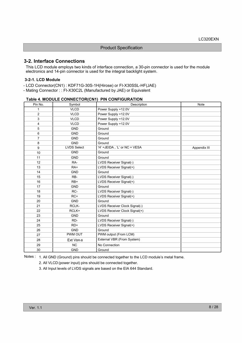
This LCD module employs two kinds of interface connection, a 30-pin connector is used for the module electronics and 14-pin connector is used for the integral backlight system.
3-2-1. LCD Module
3-2. Interface Connections
Table 4. MODULE CONNECTOR(CN1) PIN CONFIGURATION
Pin No. Symbol Description Note
1 VLCD Power Supply +12.0V
2 VLCD Power Supply +12.0V
3 VLCD Power Supply +12.0V
4 VLCD Power Supply +12.0V
5 GND Ground
6 GND Ground
7 GND Ground
8 GND Ground
9 LVDS Select ‘H’ =JEIDA , ‘L’ or NC = VESA Appendix III
10 GND Ground
11 GND Ground
12 RA- LVDS Receiver Signal(-)
13 RA+ LVDS Receiver Signal(+)
14 GND Ground
15 RB- LVDS Receiver Signal(-)
16 RB+ LVDS Receiver Signal(+)
17 GND Ground
18 RC- LVDS Receiver Signal(-)
19 RC+ LVDS Receiver Signal(+)
20 GND Ground
21 RCLK- LVDS Receiver Clock Signal(-)
22 RCLK+ LVDS Receiver Clock Signal(+)
23 GND Ground
24 RD- LVDS Receiver Signal(-)
25 RD+ LVDS Receiver Signal(+)
26 GND Ground
27 PWM OUT PWM output (From LCM)
28 Ext VBR-B External VBR (From System)
29 NC No Connection
30 GND Ground
- LCD Connector(CN1) : KDF71G-30S-1H(Hirose) or FI-X30SSL-HF(JAE)
- Mating Connector : : FI-X30C2L (Manufactured by JAE) or Equivalent
Notes : 1. All GND (Ground) pins should be connected together to the LCD module’s metal frame.
2. All VLCD (power input) pins should be connected together.
3. All Input levels of LVDS signals are based on the EIA 644 Standard.
Product Specification
9 / 28
LC320EXN
Ver. 1.1
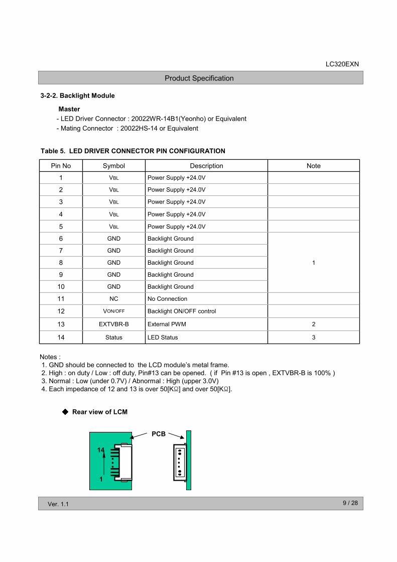
… …
PCB
14
1
Rear view of LCM
Pin No Symbol Description Note
1 VBL Power Supply +24.0V
2 VBL Power Supply +24.0V
3 VBL Power Supply +24.0V
4 VBL Power Supply +24.0V
5 VBL Power Supply +24.0V
6 GND Backlight Ground
1
7 GND Backlight Ground
8 GND Backlight Ground
9 GND Backlight Ground
10 GND Backlight Ground
11 NC No Connection
12 VON/OFF Backlight ON/OFF control
13 EXTVBR-B External PWM 2
14 Status LED Status 3
Notes :
1. GND should be connected to the LCD module’s metal frame.
2. High : on duty / Low : off duty, Pin#13 can be opened. ( if Pin #13 is open , EXTVBR-B is 100% )
3. Normal : Low (under 0.7V) / Abnormal : High (upper 3.0V)
4. Each impedance of 12 and 13 is over 50[KΩ] and over 50[KΩ].
3-2-2. Backlight Module
Table 5. LED DRIVER CONNECTOR PIN CONFIGURATION
Master
- LED Driver Connector : 20022WR-14B1(Yeonho) or Equivalent
- Mating Connector : 20022HS-14 or Equivalent
Product Specification
10 / 28
LC320EXN
Ver. 1.1
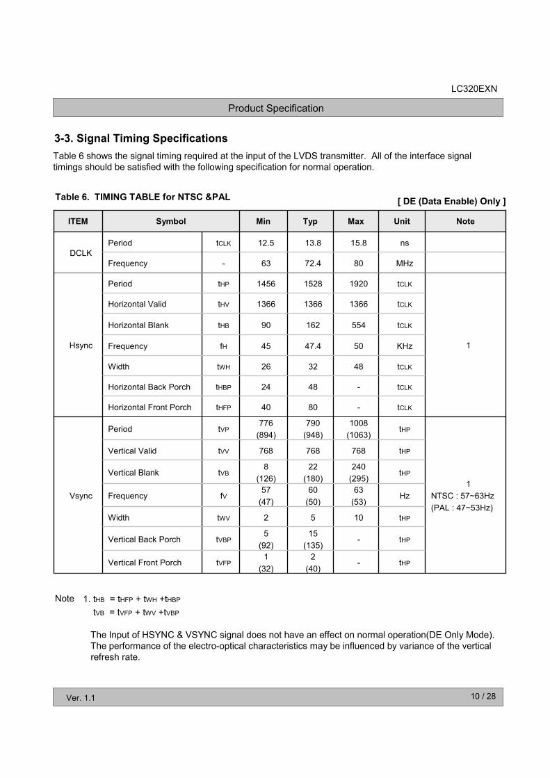
3-3. Signal Timing Specifications
Table 6 shows the signal timing required at the input of the LVDS transmitter. All of the interface signal
timings should be satisfied with the following specification for normal operation.
Table 6. TIMING TABLE for NTSC &PAL [ DE (Data Enable) Only ]
1
tCLK55416290tHBHorizontal Blank
tCLK136613661366tHVHorizontal Valid
tHP240
(295)
22
(180)
8
(126)tVB Vertical Blank
tHP768768768tVVVertical Valid
tHP1052tWVWidth
Hz63
(53)
60
(50)
57
(47)fVFrequency
tHP1008
(1063)
790
(948)
776
(894)tVPPeriod
tCLK-4824tHBPHorizontal Back Porch
tCLK-8040tHFPHorizontal Front Porch
tCLK483226tWHWidth
tHP
KHz
tHP-15
(135)
5
(92)tVBPVertical Back Porch
-2
(40)
1
(32)tVFPVertical Front Porch
5047.445fHFrequency
tCLK192015281456tHPPeriod
Hsync
1
NTSC : 57~63Hz
(PAL : 47~53Hz)
Vsync
MHz8072.463-Frequency
ns15.813.812.5tCLKPeriod
DCLK
NoteUnitMaxTypMinSymbolITEM
1. tHB = tHFP + tWH +tHBP
tVB = tVFP + tWV +tVBP
The Input of HSYNC & VSYNC signal does not have an effect on normal operation(DE Only Mode).
The performance of the electro-optical characteristics may be influenced by variance of the vertical
refresh rate.
Note
Product Specification
11 / 28
LC320EXN
Ver. 1.1
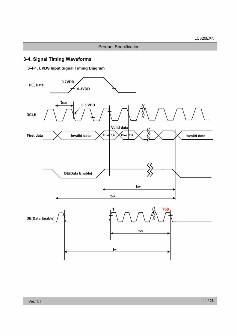
3-4. Signal Timing Waveforms
3-4-1. LVDS Input Signal Timing Diagram
0.7VDD
0.3VDD
tCLK
Invalid data
Valid data
Invalid dataPixel 0,0 Pixel 2,0
DE(Data Enable)
0.5 VDD
tHP
DE(Data Enable)
DCLK
First data
DE, Data
tHV
tVV
tVP
1 768
Product Specification
12 / 28
LC320EXN
Ver. 1.1
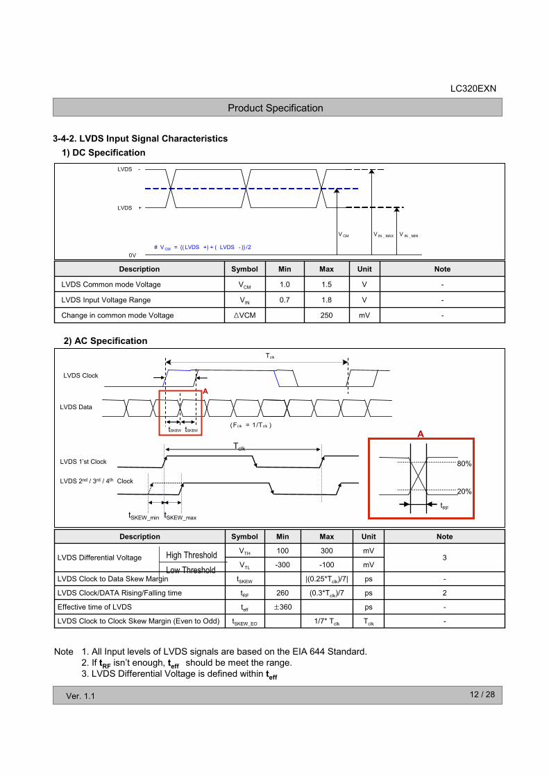
1) DC Specification
2) AC Specification
-V1.80.7VINLVDS Input Voltage Range
-mV250ΔVCMChange in common mode Voltage
-V1.51.0VCMLVDS Common mode Voltage
NoteUnitMaxMinSymbolDescription
LVDS 1’st Clock
Tclk
LVDS 2nd / 3rd / 4th Clock
tSKEW_min tSKEW_max
20%
80%
A
tRF
LVDS Data
tSKEW
LVDS Clock
Tclk
(Fclk = 1/Tclk )tSKEW
A
1. All Input levels of LVDS signals are based on the EIA 644 Standard.
2. If tRF isn’t enough, teff should be meet the range.
3. LVDS Differential Voltage is defined within teff
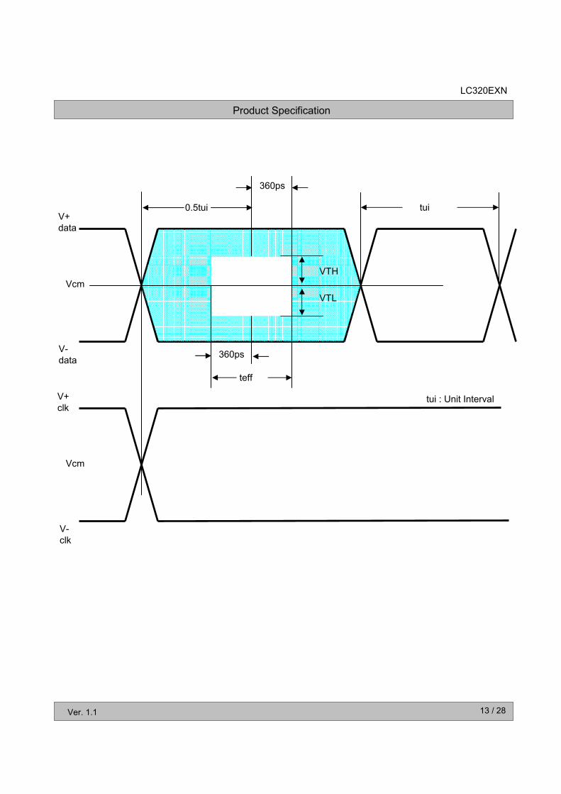
3mV300100VTH
LVDS Differential VoltagemV-100-300VTL
-ps±360teffEffective time of LVDS
NoteUnitMaxMinSymbolDescription
-ps|(0.25*Tclk)/7|tSKEWLVDS Clock to Data Skew Margin
-
2
Tclk1/7* TclktSKEW_EOLVDS Clock to Clock Skew Margin (Even to Odd)
260 ps(0.3*Tclk)/7tRFLVDS Clock/DATA Rising/Falling time
LVDS +
LVDS -
0V
V CM
# V CM = ( LVDS +) + ( LVDS - ) /2
V IN _MAX V IN _MIN
High Threshold
Low Threshold
Note
3-4-2. LVDS Input Signal Characteristics
Product Specification
13 / 28
LC320EXN
Ver. 1.1
V+
data
V-
data
Vcm
tui0.5tui
360ps
360ps
tui : Unit Interval
teff
V+
clk
V-
clk
Vcm
VTH
VTL
Product Specification
14 / 28
LC320EXN
Ver. 1.1
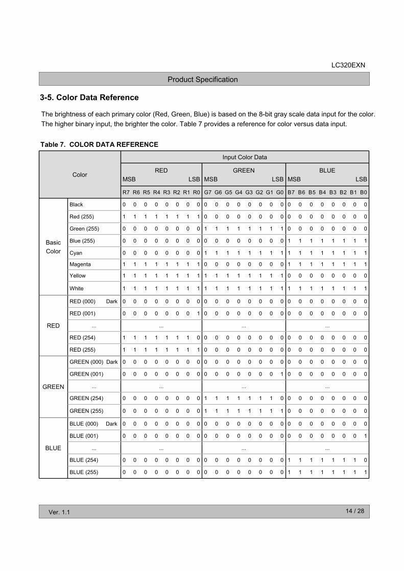
The brightness of each primary color (Red, Green, Blue) is based on the 8-bit gray scale data input for the color.
The higher binary input, the brighter the color. Table 7 provides a reference for color versus data input.
Table 7. COLOR DATA REFERENCE
Color
Input Color Data
RED
MSB LSB
GREEN
MSB LSB
BLUE
MSB LSB
R7 R6 R5 R4 R3 R2 R1 R0 G7 G6 G5 G4 G3 G2 G1 G0 B7 B6 B5 B4 B3 B2 B1 B0
Basic
Color
Black 0 0 0 0 0 0 0 0 0 0 0 0 0 0 0 0 0 0 0 0 0 0 0 0
Red (255) 1 1 1 1 1 1 1 1 0 0 0 0 0 0 0 0 0 0 0 0 0 0 0 0
Green (255) 0 0 0 0 0 0 0 0 1 1 1 1 1 1 1 1 0 0 0 0 0 0 0 0
Blue (255) 0 0 0 0 0 0 0 0 0 0 0 0 0 0 0 0 1 1 1 1 1 1 1 1
Cyan 0 0 0 0 0 0 0 0 1 1 1 1 1 1 1 1 1 1 1 1 1 1 1 1
Magenta 1 1 1 1 1 1 1 1 0 0 0 0 0 0 0 0 1 1 1 1 1 1 1 1
Yellow 1 1 1 1 1 1 1 1 1 1 1 1 1 1 1 1 0 0 0 0 0 0 0 0
White 1 1 1 1 1 1 1 1 1 1 1 1 1 1 1 1 1 1 1 1 1 1 1 1
RED
RED (000) Dark 0 0 0 0 0 0 0 0 0 0 0 0 0 0 0 0 0 0 0 0 0 0 0 0
RED (001) 0 0 0 0 0 0 0 1 0 0 0 0 0 0 0 0 0 0 0 0 0 0 0 0
... ... ... ...
RED (254) 1 1 1 1 1 1 1 0 0 0 0 0 0 0 0 0 0 0 0 0 0 0 0 0
RED (255) 1 1 1 1 1 1 1 1 0 0 0 0 0 0 0 0 0 0 0 0 0 0 0 0
GREEN
GREEN (000) Dark 0 0 0 0 0 0 0 0 0 0 0 0 0 0 0 0 0 0 0 0 0 0 0 0
GREEN (001) 0 0 0 0 0 0 0 0 0 0 0 0 0 0 0 1 0 0 0 0 0 0 0 0
... ... ... ...
GREEN (254) 0 0 0 0 0 0 0 0 1 1 1 1 1 1 1 0 0 0 0 0 0 0 0 0
GREEN (255) 0 0 0 0 0 0 0 0 1 1 1 1 1 1 1 1 0 0 0 0 0 0 0 0
BLUE
BLUE (000) Dark 0 0 0 0 0 0 0 0 0 0 0 0 0 0 0 0 0 0 0 0 0 0 0 0
BLUE (001) 0 0 0 0 0 0 0 0 0 0 0 0 0 0 0 0 0 0 0 0 0 0 0 1
... ... ... ...
BLUE (254) 0 0 0 0 0 0 0 0 0 0 0 0 0 0 0 0 1 1 1 1 1 1 1 0
BLUE (255) 0 0 0 0 0 0 0 0 0 0 0 0 0 0 0 0 1 1 1 1 1 1 1 1
3-5. Color Data Reference
Product Specification
15 / 28
LC320EXN
Ver. 1.1
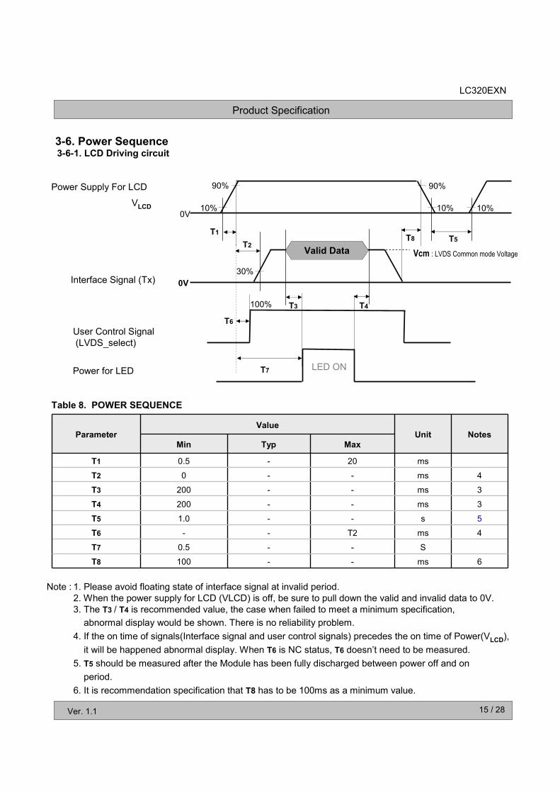
3-6. Power Sequence3-6-1. LCD Driving circuit
S--0.5T7
ParameterValue
Unit Notes
Min Typ Max
T1 0.5 - 20 ms
T2 0 - - ms 4
T3 200 - - ms 3
T4 200 - - ms 3
T5 1.0 - - s 5
T6 - - T2 ms 4
T8 100 - - ms 6
Table 8. POWER SEQUENCE
10%0V
90%
10%
T1
T2T5
LED ON
T3 T4
T6
Interface Signal (Tx)
Power for LED
Power Supply For LCD
VLCD
User Control Signal
(LVDS_select)
0V
Valid Data
100%
1. Please avoid floating state of interface signal at invalid period.
2. When the power supply for LCD (VLCD) is off, be sure to pull down the valid and invalid data to 0V.
3. The T3 / T4 is recommended value, the case when failed to meet a minimum specification,
abnormal display would be shown. There is no reliability problem.
4. If the on time of signals(Interface signal and user control signals) precedes the on time of Power(VLCD),
it will be happened abnormal display. When T6 is NC status, T6 doesn’t need to be measured.
5. T5 should be measured after the Module has been fully discharged between power off and on
period.
6. It is recommendation specification that T8 has to be 100ms as a minimum value.
Note :
T7
30%
Vcm : LVDS Common mode Voltage
10%
T8
90%
Product Specification
16 / 28
LC320EXN
Ver. 1.1
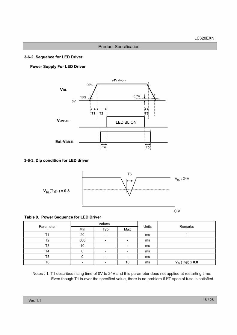
3-6-2. Sequence for LED Driver
Notes : 1. T1 describes rising time of 0V to 24V and this parameter does not applied at restarting time.
Even though T1 is over the specified value, there is no problem if I2T spec of fuse is satisfied.
Power Supply For LED Driver
3-6-3. Dip condition for LED driver
VON/OFF
VBL
10%
0V
90%
T1 T2
0.7V
T4
24V (typ.)
T3
LED BL ON
Ext-VBR-B
T5
Table 9. Power Sequence for LED Driver
VBL(Typ.) x 0.8
0 V
VBL : 24V
T6
ms--0T5
VBL(Typ) x 0.8ms10--T6
-
ms--0T4
ms10T3
1
Remarks
ms--500T2
ms--20T1
MaxTypMinUnits
ValuesParameter
Product Specification
17 / 28
LC320EXN
Ver. 1.1
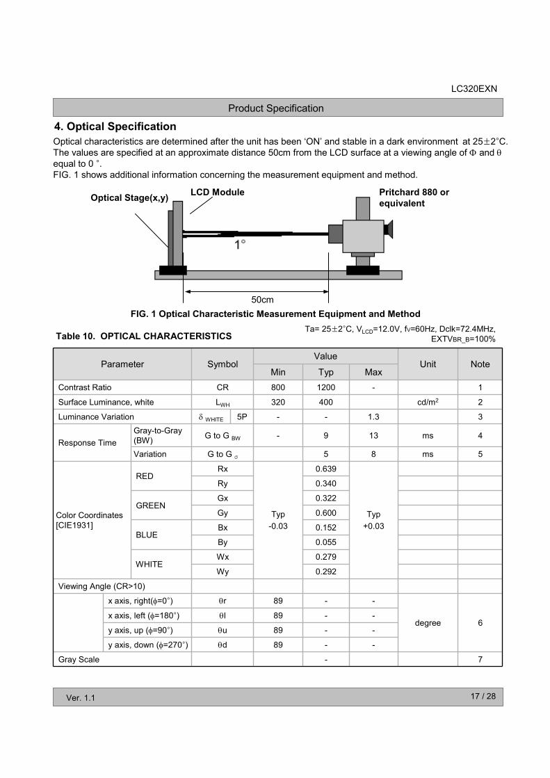
Table 10. OPTICAL CHARACTERISTICS
LCD ModuleOptical Stage(x,y)
Pritchard 880 or
equivalent
50cm
FIG. 1 Optical Characteristic Measurement Equipment and Method
4. Optical Specification
Optical characteristics are determined after the unit has been ‘ON’ and stable in a dark environment at 25±2°C. The values are specified at an approximate distance 50cm from the LCD surface at a viewing angle of Φ and θ
equal to 0 °. FIG. 1 shows additional information concerning the measurement equipment and method.
Ta= 25±2°C, VLCD=12.0V, fV=60Hz, Dclk=72.4MHz,EXTVBR_B=100%
Parameter SymbolValue
Unit NoteMin Typ Max
Contrast Ratio CR 800 1200 - 1
Surface Luminance, white LWH 320 400 cd/m2 2
Luminance Variation δ WHITE 5P - - 1.3 3
Response Time
Gray-to-Gray
(BW)G to G BW - 9 13 ms 4
Variation G to G σ 5 8 ms 5
Color Coordinates
[CIE1931]
REDRx
Typ
-0.03
0.639
Typ
+0.03
Ry 0.340
GREENGx 0.322
Gy 0.600
BLUE Bx 0.152
By 0.055
WHITEWx 0.279
Wy 0.292
Viewing Angle (CR>10)
x axis, right(φ=0°) θr 89 - -
degree 6x axis, left (φ=180°) θl 89 - -
y axis, up (φ=90°) θu 89 - -
y axis, down (φ=270°) θd 89 - -
Gray Scale - 7
Product Specification
18 / 28
LC320EXN
Ver. 1.1
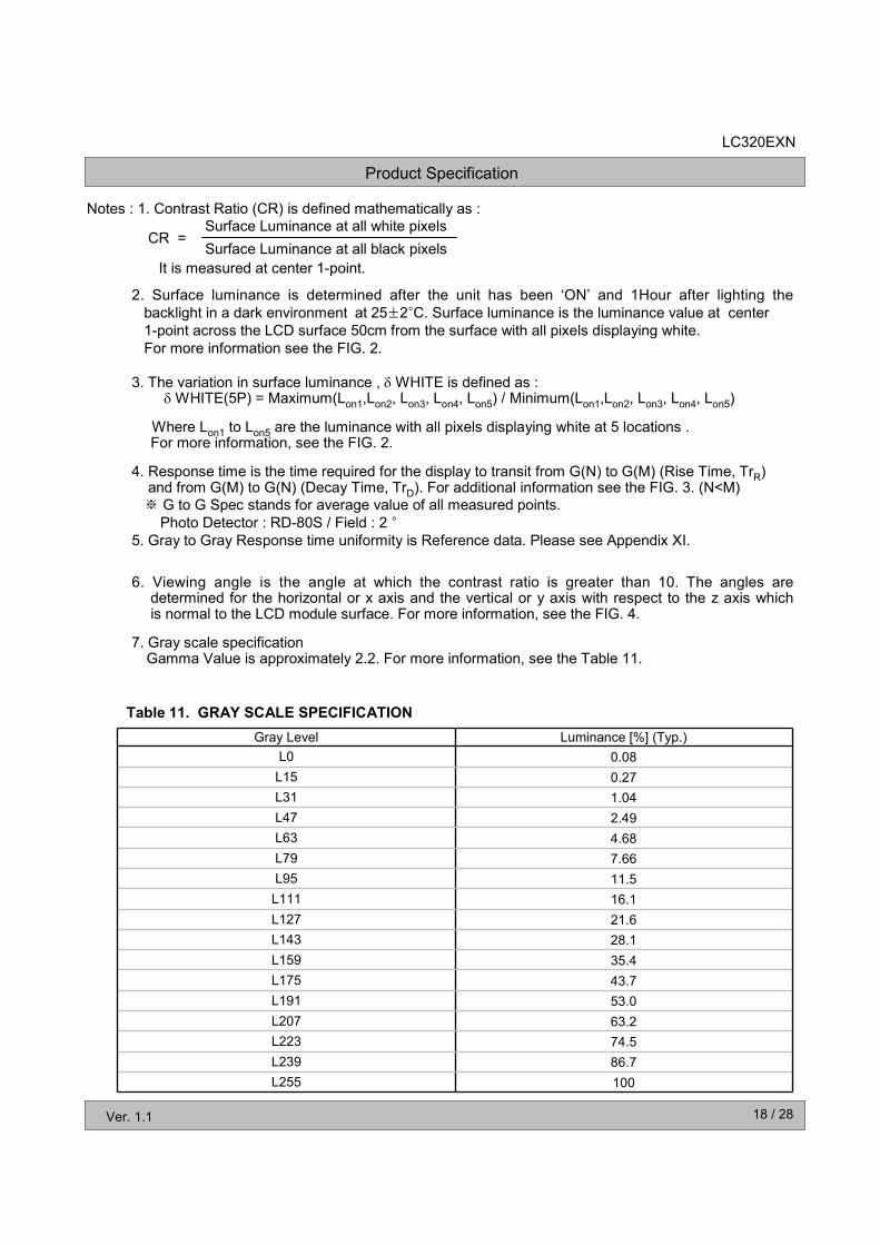
Table 11. GRAY SCALE SPECIFICATION
Gray Level Luminance [%] (Typ.)
L0 0.08
L15 0.27
L31 1.04
L47 2.49
L63 4.68
L79 7.66
L95 11.5
L111 16.1
L127 21.6
L143 28.1
L159 35.4
L175 43.7
L191 53.0
L207 63.2
L223 74.5
L239 86.7
L255 100
Notes : 1. Contrast Ratio (CR) is defined mathematically as :
Surface Luminance at all white pixelsCR =
Surface Luminance at all black pixels
It is measured at center 1-point.
2. Surface luminance is determined after the unit has been ‘ON’ and 1Hour after lighting the
backlight in a dark environment at 25±2°C. Surface luminance is the luminance value at center 1-point across the LCD surface 50cm from the surface with all pixels displaying white.
For more information see the FIG. 2.
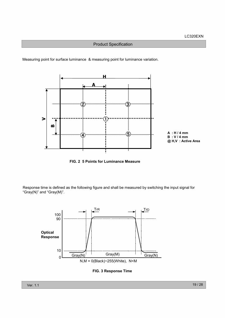
3. The variation in surface luminance , δWHITE is defined as :δWHITE(5P) = Maximum(Lon1,Lon2, Lon3, Lon4, Lon5) / Minimum(Lon1,Lon2, Lon3, Lon4, Lon5)
Where Lon1 to Lon5 are the luminance with all pixels displaying white at 5 locations . For more information, see the FIG. 2.
4. Response time is the time required for the display to transit from G(N) to G(M) (Rise Time, TrR) and from G(M) to G(N) (Decay Time, TrD). For additional information see the FIG. 3. (N<M)
※ G to G Spec stands for average value of all measured points. Photo Detector : RD-80S / Field : 2 °
5. Gray to Gray Response time uniformity is Reference data. Please see Appendix XI.
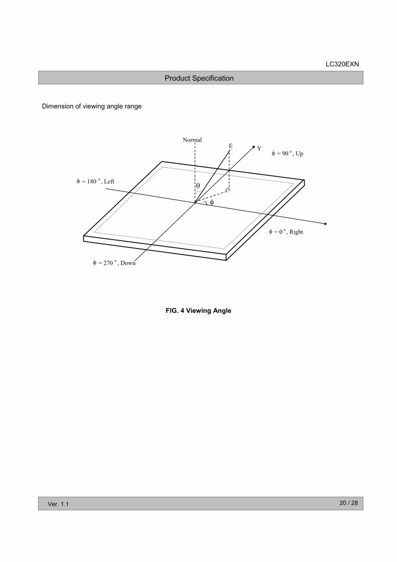
6. Viewing angle is the angle at which the contrast ratio is greater than 10. The angles aredetermined for the horizontal or x axis and the vertical or y axis with respect to the z axis whichis normal to the LCD module surface. For more information, see the FIG. 4.
7. Gray scale specificationGamma Value is approximately 2.2. For more information, see the Table 11.
Product Specification
19 / 28
LC320EXN
Ver. 1.1
FIG. 3 Response Time
Response time is defined as the following figure and shall be measured by switching the input signal for
“Gray(N)” and “Gray(M)”.
Measuring point for surface luminance & measuring point for luminance variation.
FIG. 2 5 Points for Luminance Measure
H
A
V
B
①①①①
③③③③②②②②
⑤⑤⑤⑤④④④④
Gray(M)Gray(N)
TrR TrD
10090
10
0
Optical
Response
N,M = 0(Black)~255(White), N<M
Gray(N)
A : H / 4 mm
B : V / 4 mm
@ H,V : Active Area
Product Specification
20 / 28
LC320EXN
Ver. 1.1
FIG. 4 Viewing Angle
Dimension of viewing angle range
Normal
Y E
φ
θ
φ = 0 °, Right
φ = 180 °, Left
φ = 270 °, Down
φ = 90 °, Up
Product Specification
21 / 28
LC320EXN
Ver. 1.1
Table 12 provides general mechanical characteristics.
5. Mechanical Characteristics
Table 12. MECHANICAL CHARACTERISTICS
Item Value
Outline Dimension
Horizontal 741.4mm
Vertical 435.8 mm
Depth 23.6 mm
Bezel AreaHorizontal 705.4mm
Vertical 399.8mm
Active Display AreaHorizontal 697.685mm
Vertical 392.256mm
Weight 5,900 g (Typ.), 6,200 g (Max.)
Note : 1.Please refer to a mechanical drawing in terms of tolerance at the next page.
Product Specification
22 / 28
LC320EXN
Ver. 1.1
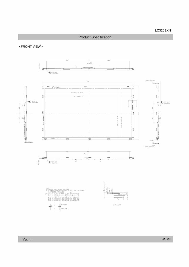
<FRONT VIEW>
Product Specification
23 / 28
LC320EXN
Ver. 1.1
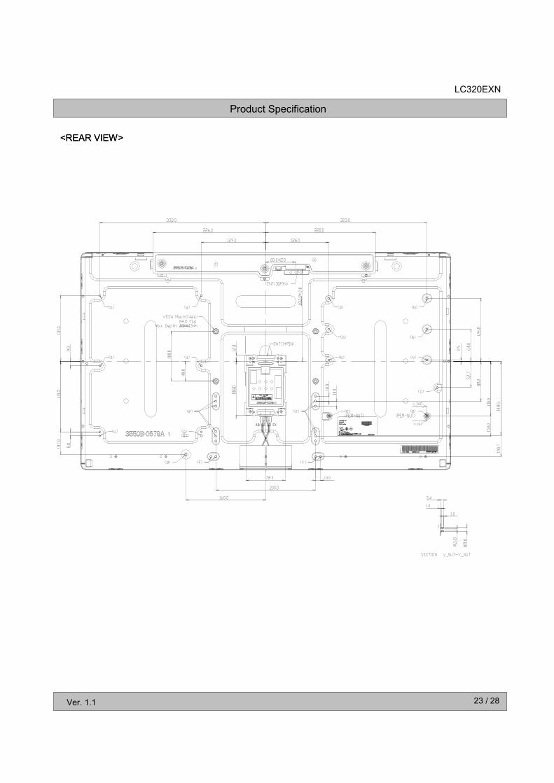
<REAR VIEW><REAR VIEW>
Product Specification
24 / 28
LC320EXN
Ver. 1.1
6. Reliability
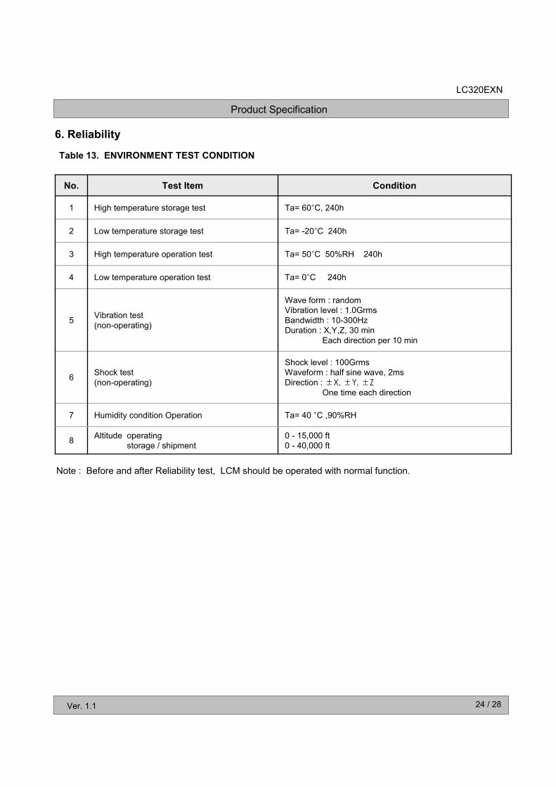
Table 13. ENVIRONMENT TEST CONDITION
Note : Before and after Reliability test, LCM should be operated with normal function.
0 - 15,000 ft
0 - 40,000 ft
Altitude operating
storage / shipment8
Ta= 40 °C ,90%RHHumidity condition Operation7
Shock level : 100Grms
Waveform : half sine wave, 2ms
Direction :±X, ±Y, ±ZOne time each direction
Shock test
(non-operating)6
Wave form : random
Vibration level : 1.0Grms
Bandwidth : 10-300Hz
Duration : X,Y,Z, 30 min
Each direction per 10 min
Vibration test
(non-operating)5
Ta= 0°C 240hLow temperature operation test4
Ta= 50°C 50%RH 240hHigh temperature operation test3
Ta= -20°C 240hLow temperature storage test2
Ta= 60°C, 240h High temperature storage test1
ConditionTest ItemNo.
Product Specification
25 / 28
LC320EXN
Ver. 1.1
7. International Standards
7-1. Safety
7-3. Environment
a) RoHS, Directive 2002/95/EC of the European Parliament and of the council of 27 January 2003
7-2. EMC
a) ANSI C63.4 “American National Standard for Methods of Measurement of Radio-Noise
Emissions from Low-Voltage Electrical and Electronic Equipment in the Range of 9 kHz to 40 GHz.”
American National Standards Institute (ANSI), 2003.
b) CISPR 22 “Information technology equipment – Radio disturbance characteristics – Limit and
methods of measurement." International Special Committee on Radio Interference
(CISPR), 2005.
c) CISPR 13 “Sound and television broadcast receivers and associated equipment – Radio disturbance
characteristics – Limits and method of measurement." International Special Committee on Radio
Interference (CISPR), 2006.
a) UL 60065, Seventh Edition, Underwriters Laboratories Inc.
Audio, Video and Similar Electronic Apparatus - Safety Requirements.
b) CAN/CSA C22.2 No.60065:03, Canadian Standards Association.
Audio, Video and Similar Electronic Apparatus - Safety Requirements.
c) EN 60065:2002 + A11:2008, European Committee for Electrotechnical Standardization (CENELEC).
Audio, Video and Similar Electronic Apparatus - Safety Requirements.
Class 1M LED Product
IEC60825-1 : 2001
Embedded LED Power (Class1M)
Power : 6.4145 mW (Max.)
Wavelength : 447, 277 ~526 (nm)
Width : 1.2 x 0.55 (mm)
Notes
1. Laser (LED Backlight) Information (SEOUL SEMICONDUCTOR, EWT719P)
2. Caution
: LED inside.
Class 1M laser (LEDs) radiation when open.
Do not open while operating.
d) IEC 60065:2005 + A1:2005, The International Electrotechnical Commission (IEC).
Audio, Video and Similar Electronic Apparatus - Safety Requirements.
(Including report of IEC60825-1:2001 clause 8 and clause 9)
Product Specification
26 / 28
LC320EXN
Ver. 1.1
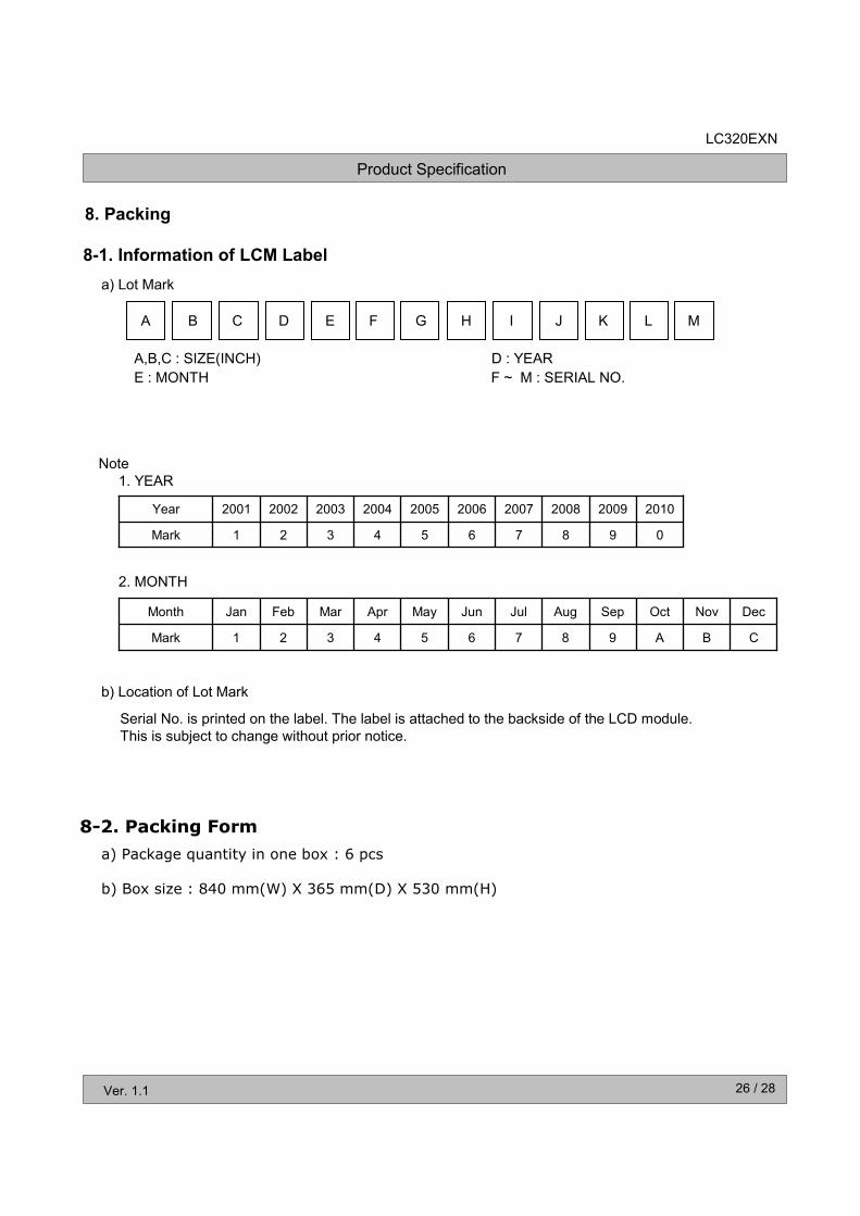
Note
1. YEAR
2. MONTH
Mark
Year
0
2010
6
2006
7
2007
8
2008
9
2009
4
2004
5
2005
321
200320022001
B
Nov
Mark
Month
A
Oct
6
Jun
7
Jul
8
Aug
9
Sep
4
Apr
5
May
C321
DecMarFebJan
b) Location of Lot Mark
Serial No. is printed on the label. The label is attached to the backside of the LCD module.
This is subject to change without prior notice.
8. Packing
8-2. Packing Form
8-1. Information of LCM Label
a) Lot Mark
A B C D E F G H I J K L M
A,B,C : SIZE(INCH) D : YEAR
E : MONTH F ~ M : SERIAL NO.
a) Package quantity in one box : 6 pcs
b) Box size : 840 mm(W) X 365 mm(D) X 530 mm(H)
Product Specification
27 / 28
LC320EXN
Ver. 1.1
Please pay attention to the followings when you use this TFT LCD module.
9-1. Mounting Precautions
(1)You must mount a module using specified mounting holes (Details refer to the drawings).
(2) You should consider the mounting structure so that uneven force (ex. Twisted stress) is not applied to the
module. And the case on which a module is mounted should have sufficient strength so that external
force is not transmitted directly to the module.
(3) Please attach the surface transparent protective plate to the surface in order to protect the polarizer.
Transparent protective plate should have sufficient strength in order to the resist external force.
(4) You should adopt radiation structure to satisfy the temperature specification.
(5) Acetic acid type and chlorine type materials for the cover case are not desirable because the former
generates corrosive gas of attacking the polarizer at high temperature and the latter causes circuit break
by electro-chemical reaction.
(6) Do not touch, push or rub the exposed polarizers with glass, tweezers or anything harder than HB
pencil lead. And please do not rub with dust clothes with chemical treatment.
Do not touch the surface of polarizer for bare hand or greasy cloth.(Some cosmetics are detrimental
to the polarizer.)
(7) When the surface becomes dusty, please wipe gently with absorbent cotton or other soft materials like
chamois soaks with petroleum benzine. Normal-hexane is recommended for cleaning the adhesives
used to attach front / rear polarizers. Do not use acetone, toluene and alcohol because they cause
chemical damage to the polarizer. * There is no problem of Panel crack under 5kgf / φ10mm (8) Wipe off saliva or water drops as soon as possible. Their long time contact with polarizer causes
deformations and color fading.
(9) Do not open the case because inside circuits do not have sufficient strength.
9-2. Operating Precautions
(1) The spike noise causes the mis-operation of circuits. It should be lower than following voltage :
V=±200mV(Over and under shoot voltage)(2) Response time depends on the temperature.(In lower temperature, it becomes longer.)
(3) Brightness depends on the temperature. (In lower temperature, it becomes lower.)
And in lower temperature, response time(required time that brightness is stable after turned on) becomes
longer.
(4) Be careful for condensation at sudden temperature change. Condensation makes damage to polarizer or
electrical contacted parts. And after fading condensation, smear or spot will occur.
(5) When fixed patterns are displayed for a long time, remnant image is likely to occur.
(6) Module has high frequency circuits. Sufficient suppression to the electromagnetic interference shall be
done by system manufacturers. Grounding and shielding methods may be important to minimized the
interference.
(7) Please do not give any mechanical and/or acoustical impact to LCM. Otherwise, LCM can’t be operated
its full characteristics perfectly.
(8) A screw which is fastened up the steels should be a machine screw.
(if not, it causes metallic foreign material and deal LCM a fatal blow)
(9) Please do not set LCD on its edge.
(10) The conductive material and signal cables are kept away from LED driver inductor to prevent abnormal
display, sound noise and temperature rising.
9. Precautions
Product Specification
28 / 28
LC320EXN
Ver. 1.1
Since a module is composed of electronic circuits, it is not strong to electrostatic discharge. Make certain that
treatment persons are connected to ground through wrist band etc. And don’t touch interface pin directly.
9-3. Electrostatic Discharge Control
Strong light exposure causes degradation of polarizer and color filter.
9-4. Precautions for Strong Light Exposure
When storing modules as spares for a long time, the following precautions are necessary.
(1) Store them in a dark place. Do not expose the module to sunlight or fluorescent light. Keep the temperature
between 5°C and 35°C at normal humidity.(2) The polarizer surface should not come in contact with any other object.
It is recommended that they be stored in the container in which they were shipped.
9-5. Storage
9-6. Handling Precautions for Protection Film
(1) The protection film is attached to the bezel with a small masking tape.
When the protection film is peeled off, static electricity is generated between the film and polarizer.
This should be peeled off slowly and carefully by people who are electrically grounded and with well ion-
blown equipment or in such a condition, etc.
(2) When the module with protection film attached is stored for a long time, sometimes there remains a very
small amount of glue still on the bezel after the protection film is peeled off.
(3) You can remove the glue easily. When the glue remains on the bezel surface or its vestige is recognized,
please wipe them off with absorbent cotton waste or other soft material like chamois soaked with normal-
hexane.
Product Specification
29 / 28
LC320EXN
Ver. 1.1
# APPENDIX- I
Package
NO. DESCRIPTION MATERIAL
1 LCD Module
2 BAG AL
3 TAPE MASKING 20MMX50M
4 Packing EPS
5 Packing EPS
6 BOX PAPER(DW)
7 TAPE OPP 70MMX300M
8 Label ART 100X70
LLDPEWrap15
NO. DESCRIPTION MATERIAL
9 PACKING ASS’Y
10 PALLET Plywood
11 ANGLE, COVER PAPER(SW)
12 LABEL ART 100X70
13 BAND PP
14 CLIP, BAND STEEL
※※※※ Packing Ass`yPacking Ass`yPacking Ass`yPacking Ass`y ※※※※ Pallet Ass`yPallet Ass`yPallet Ass`yPallet Ass`y
Palletizing Size : 1140 X 870 X 1180.5
Box Quantity : 6 ea
Product Specification
30 / 28
LC320EXN
Ver. 1.1
# APPENDIX- II-1
LCM Label
Model
Serial No.
UL, TUV Mark
LGD Logo
Origin
RoHS Verified
MADE IN KOREA
LC320EXN(SC)(A1)
US PATENT No.
LIGHT GUIDE : >PMMA<
************* ***
Product Specification
31 / 28
LC320EXN
Ver. 1.1
# APPENDIX- II-2
Box Label Pallet Label
LC320EXN
SCA1
6 pcs
LC320EXN
SCA1
36 pcs
Product Specification
32 / 28
LC320EXN
Ver. 1.1
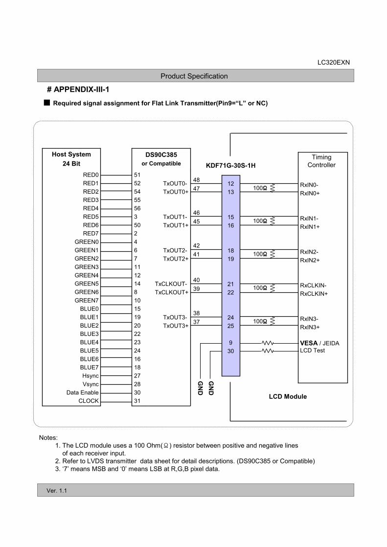
# APPENDIX-III-1
Required signal assignment for Flat Link Transmitter(Pin9=“L” or NC)
RED0
RED1
RED2
RED3
RED4
RED5
RED6
RED7
GREEN0
GREEN1
GREEN2
GREEN3
GREEN4
GREEN5
GREEN6
GREEN7
BLUE0
BLUE1
BLUE2
BLUE3
BLUE4
BLUE5
BLUE6
BLUE7
Hsync
Vsync
Data Enable
CLOCK
Host System
24 Bit
TxOUT0-
TxOUT0+
TxOUT1-
TxOUT1+
TxOUT2-
TxOUT2+
TxCLKOUT-
TxCLKOUT+
TxOUT3-
TxOUT3+
51
52
54
55
56
3
50
2
4
6
7
11
12
14
8
10
15
19
20
22
23
24
16
18
27
28
30
31
DS90C385
or Compatible
12
13
15
16
18
19
21
22
24
25
9
30
RxIN0-
RxIN0+
RxIN1-
RxIN1+
RxIN2-
RxIN2+
RxCLKIN-
RxCLKIN+
RxIN3-
RxIN3+
VESA / JEIDA LCD Test
100ΩΩΩΩ
100ΩΩΩΩ
100ΩΩΩΩ
100ΩΩΩΩ
100ΩΩΩΩ
48
47
46
45
42
41
40
39
38
37
KDF71G-30S-1H
Timing
Controller
LCD Module
GND
GND
Notes:
1. The LCD module uses a 100 Ohm(Ω) resistor between positive and negative linesof each receiver input.
2. Refer to LVDS transmitter data sheet for detail descriptions. (DS90C385 or Compatible)
3. ‘7’ means MSB and ‘0’ means LSB at R,G,B pixel data.
Product Specification
33 / 28
LC320EXN
Ver. 1.1
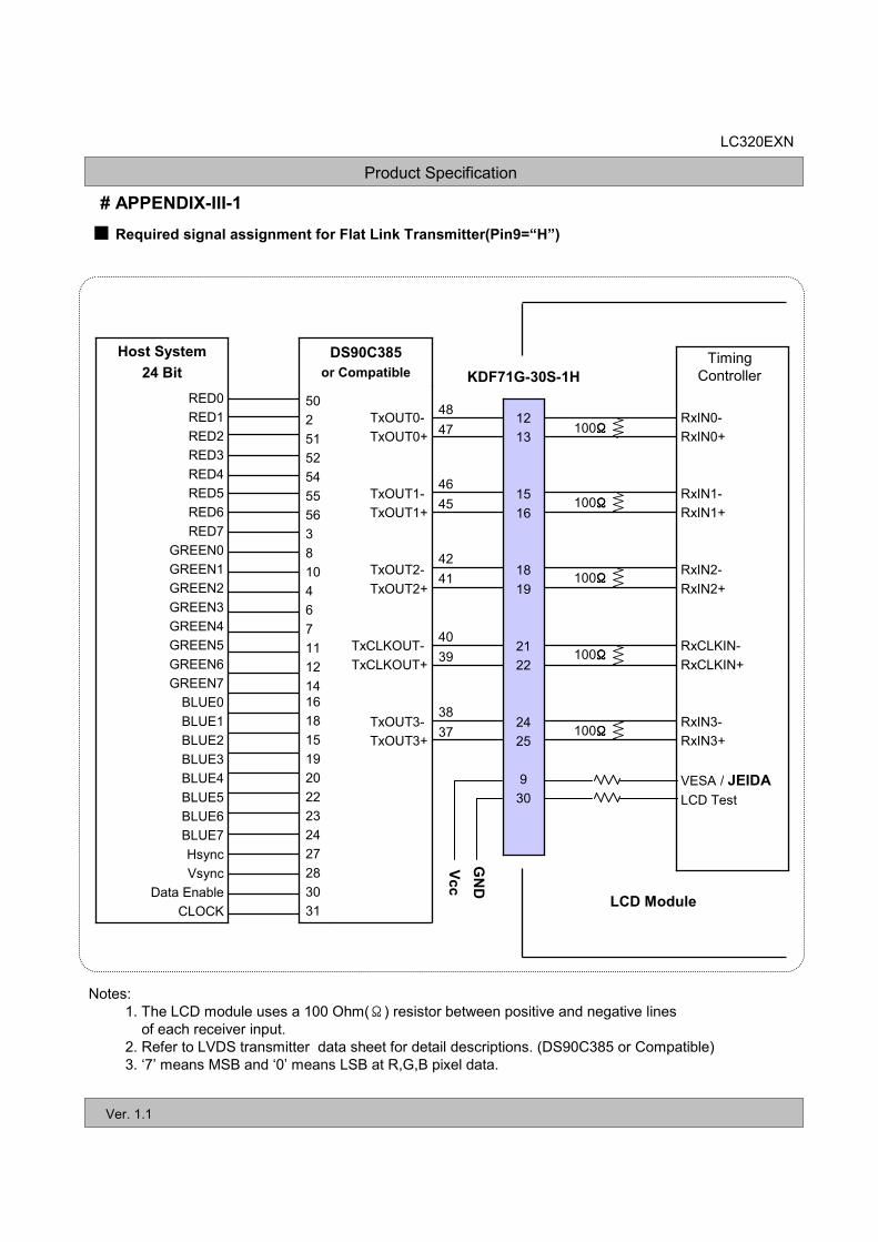
# APPENDIX-III-1
Required signal assignment for Flat Link Transmitter(Pin9=“H”)
RED0
RED1
RED2
RED3
RED4
RED5
RED6
RED7
GREEN0
GREEN1
GREEN2
GREEN3
GREEN4
GREEN5
GREEN6
GREEN7
BLUE0
BLUE1
BLUE2
BLUE3
BLUE4
BLUE5
BLUE6
BLUE7
Hsync
Vsync
Data Enable
CLOCK
Host System
24 Bit
TxOUT0-
TxOUT0+
TxOUT1-
TxOUT1+
TxOUT2-
TxOUT2+
TxCLKOUT-
TxCLKOUT+
TxOUT3-
TxOUT3+
DS90C385
or Compatible
RxIN0-
RxIN0+
RxIN1-
RxIN1+
RxIN2-
RxIN2+
RxCLKIN-
RxCLKIN+
RxIN3-
RxIN3+
VESA / JEIDA
LCD Test
100ΩΩΩΩ
100ΩΩΩΩ
100ΩΩΩΩ
100ΩΩΩΩ
100ΩΩΩΩ
48
47
46
45
42
41
40
39
38
37
LCD Module
Vcc
GND
50
2
51
52
54
55
56
3
8
10
4
6
7
11
12
14
16
18
15
19
20
22
23
24
27
28
30
31
KDF71G-30S-1H
Timing
Controller
12
13
15
16
18
19
21
22
24
25
9
30
Notes:
1. The LCD module uses a 100 Ohm(Ω) resistor between positive and negative linesof each receiver input.
2. Refer to LVDS transmitter data sheet for detail descriptions. (DS90C385 or Compatible)
3. ‘7’ means MSB and ‘0’ means LSB at R,G,B pixel data.
Product Specification
34 / 28
LC320EXN
Ver. 1.1
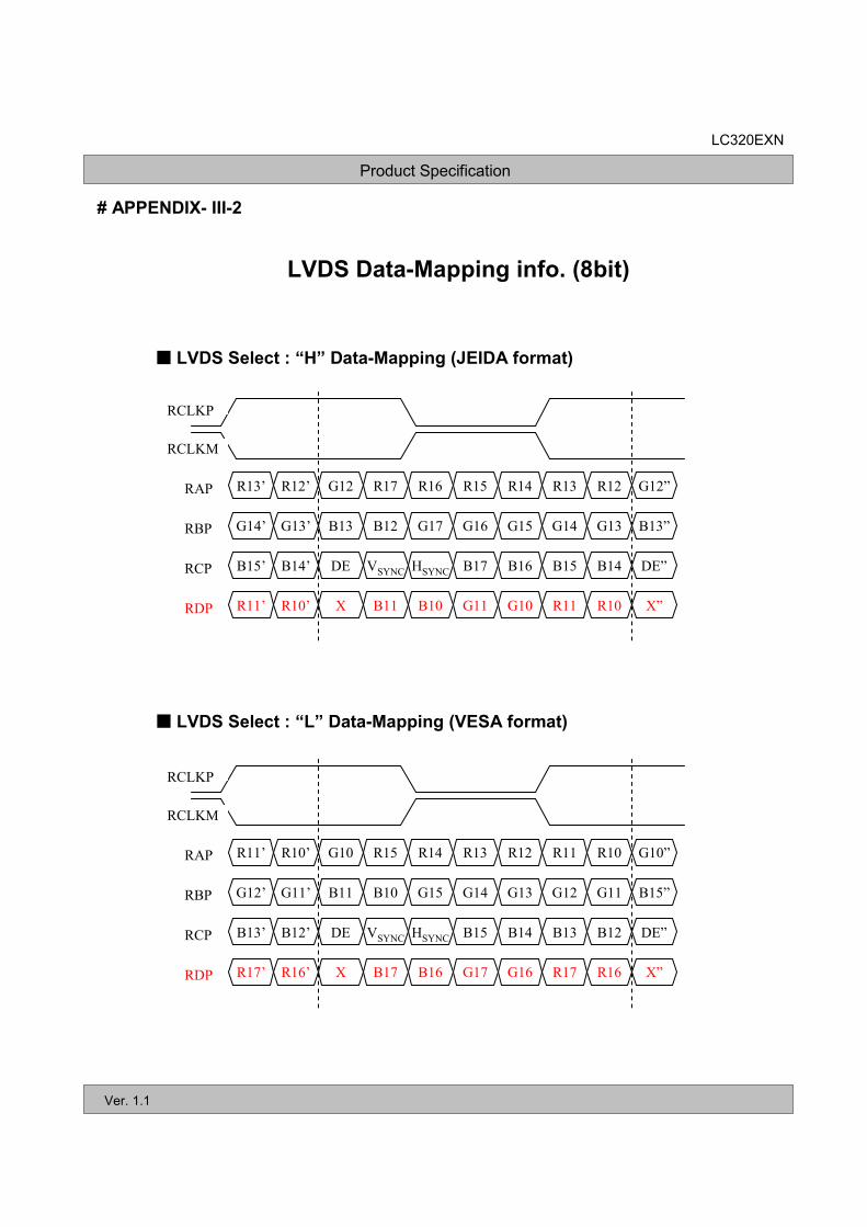
LVDS Select : “H” Data-Mapping (JEIDA format)
LVDS Select : “L” Data-Mapping (VESA format)
R17 R16 R15 R14G12 R13R12’ R12R13’ G12”
B12 G17 G16 G15B13 G14G13’ G13G14’ B13”
VSYNC HSYNC B17 B16DE B15B14’ B14B15’ DE”
B11 B10 G11 G10X R11R10’ R10R11’ X”
RCLKP
RCLKM
RAP
RBP
RCP
RDP
R15 R14 R13 R12G10 R11R10’ R10R11’ G10”
B10 G15 G14 G13B11 G12G11’ G11G12’ B15”
VSYNC HSYNC B15 B14DE B13B12’ B12B13’ DE”
B17 B16 G17 G16X R17R16’ R16R17’ X”
RCLKP
RCLKM
RAP
RBP
RCP
RDP
LVDS Data-Mapping info. (8bit)
# APPENDIX- III-2
Product Specification
35 / 28
LC320EXN
Ver. 1.1
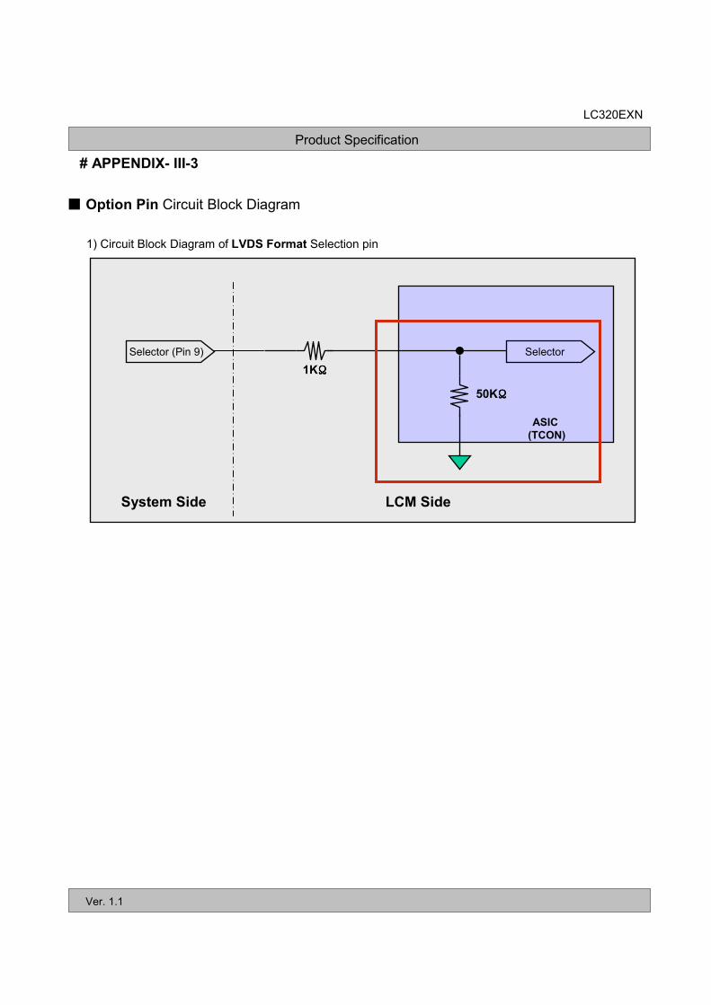
# APPENDIX- III-3
ASIC
(TCON)
System Side LCM Side
Selector (Pin 9) Selector
1KΩΩΩΩ
50KΩΩΩΩ
Option Pin Circuit Block Diagram
1) Circuit Block Diagram of LVDS Format Selection pin
Product Specification
36 / 28
LC320EXN
Ver. 1.1
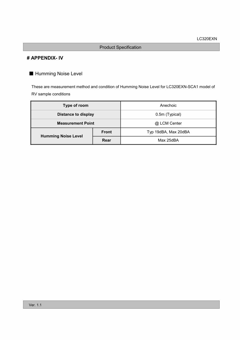
These are measurement method and condition of Humming Noise Level for LC320EXN-SCA1 model of
RV sample conditions
# APPENDIX- IV
Humming Noise Level
Rear
Front Typ 19dBA, Max 20dBAHumming Noise Level
Measurement Point
Distance to display
Type of room
Max 25dBA
@ LCM Center
0.5m (Typical)
Anechoic