Embed Size (px)
Citation preview
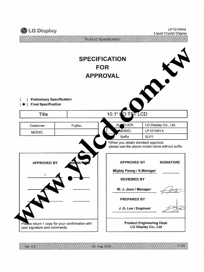
Product Specification
LP101WH4
Liquid Crystal Display
Ver. 0.5 29. Aug. 2012
SPECIFICATION
FOR
APPROVAL
Title 10.1" HD TFT LCD
Customer Fujitsu
MODEL
SUPPLIER LG Display Co., Ltd.
*MODEL LP101WH 4
Suffix SLP1
*When you obtain standard approval,
please use the above model name without suffix
( ) Preliminary Specification
( ◆ ) Final Specification
APPROVED BY SIGNATURE
/
/
/
Please return 1 copy for your confirmation with
your signature and comments.
Mighty Peang / S.Manager
Product Engineering Dept.
LG Display Co., Ltd
APPROVED BY SIGNATURE
REVIEWED BY
PREPARED BY
W. J. Jeon / Manager
J .G. Lee / Engineerwww.yslcd.com.tw
Product Specification
LP101WH4
Liquid Crystal Display
Ver. 0.5 29. Aug. 2012
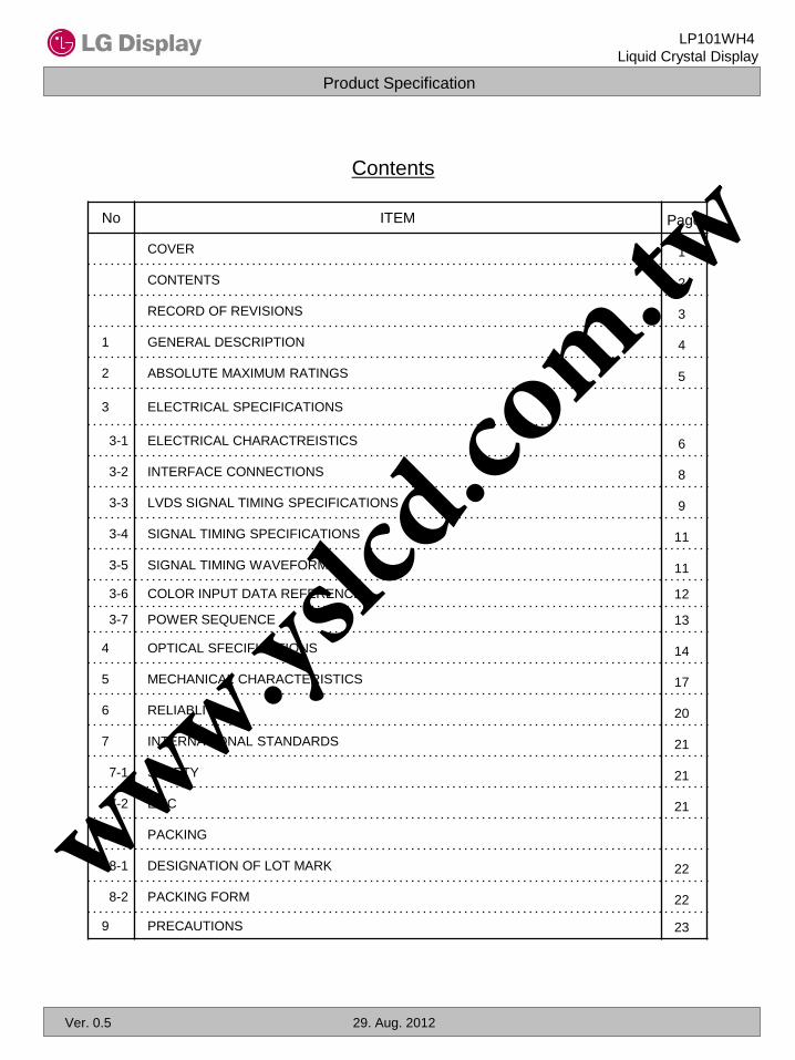
Contents
No ITEM Page
COVER 1
CONTENTS 2
RECORD OF REVISIONS 3
1 GENERAL DESCRIPTION 4
2 ABSOLUTE MAXIMUM RATINGS 5
3 ELECTRICAL SPECIFICATIONS
3-1 ELECTRICAL CHARACTREISTICS 6
3-2 INTERFACE CONNECTIONS 8
3-3 LVDS SIGNAL TIMING SPECIFICATIONS 9
3-4 SIGNAL TIMING SPECIFICATIONS 11
3-5 SIGNAL TIMING WAVEFORM 11
3-6 COLOR INPUT DATA REFERENCE 12
3-7 POWER SEQUENCE 13
4 OPTICAL SFECIFICATIONS 14
5 MECHANICAL CHARACTERISTICS 17
6 RELIABLITY 20
7 INTERNATIONAL STANDARDS 21
7-1 SAFETY 21
7-2 EMC 21
8 PACKING
8-1 DESIGNATION OF LOT MARK 22
8-2 PACKING FORM 22
9 PRECAUTIONS 23
www.yslcd.com.tw
Product Specification
LP101WH4
Liquid Crystal Display
Ver. 0.5 29. Aug. 2012
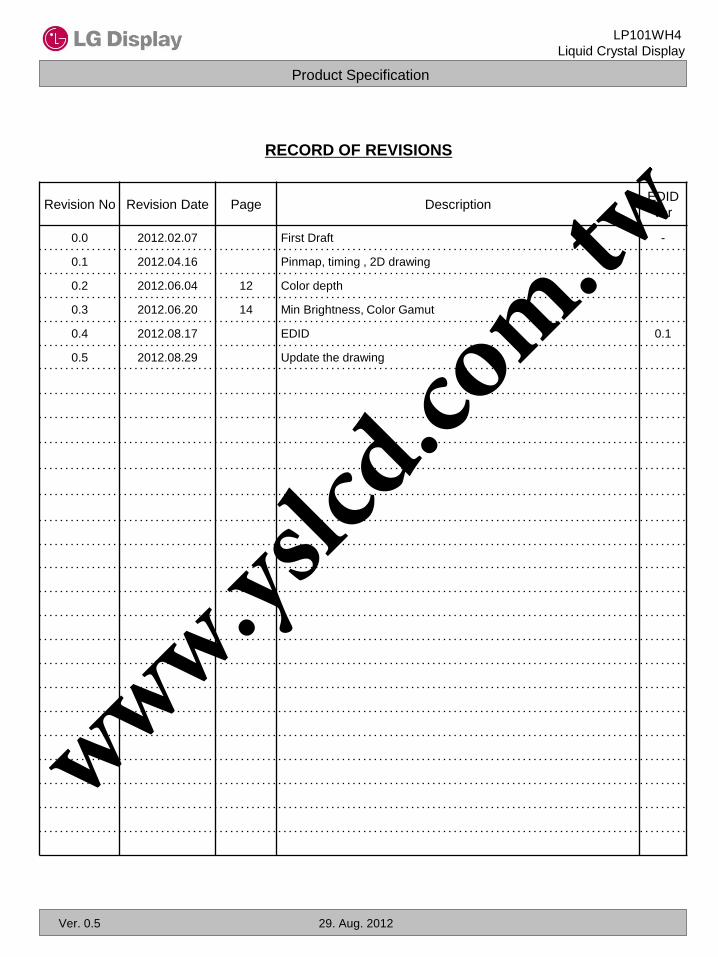
RECORD OF REVISIONS
Revision No Revision Date Page DescriptionEDID
ver
0.0 2012.02.07 First Draft -
0.1 2012.04.16 Pinmap, timing , 2D drawing
0.2 2012.06.04 12 Color depth
0.3 2012.06.20 14 Min Brightness, Color Gamut
0.4 2012.08.17 EDID 0.1
0.5 2012.08.29 Update the drawing
www.yslcd.com.tw
Product Specification
LP101WH4
Liquid Crystal Display
Ver. 0.5 29. Aug. 2012
1. General Description
General Features
Active Screen Size 10.1 inches diagonal
Outline Dimension 232.8± 0.3 (H) × 138.15± 0.3 (V) × 2.40 mm (max.)
Pixel Pitch 0.16290 mm × 0.16290 mm
Pixel Format 1366 horiz. by 768 vert. Pixels RGB strip arrangement
Color Depth 6-bit, 262,144 colors
Luminance, White 400 cd/m2(Typ)
Power Consumption Logic : 0.55 W(typ.@Mosaic), Back Light : 2.1 W (typ.@ ILED= 17.5mA)
Weight 125g ( Max )
Display Operating Mode Transmissive mode, normally Black
Surface Treatment Anti-Glare treatment (3H) of the front polarizer
The LP101WH4 is a Color Active Matrix Liquid Crystal Display with an integral LED backlight system. The
matrix employs a-Si Thin Film Transistor as the active element. It is a transmissive type display operating in
the normally Black mode. This TFT-LCD has 10.1inches diagonally measured active display area with HD
resolution(1366 horizontal by 768 vertical pixel array). Each pixel is divided into Red, Green and Blue sub-
pixels or dots which are arranged in vertical stripes. Gray scale or the brightness of the sub-pixel color is
determined with a 8-bit gray scale signal for each dot, thus, presenting a palette of more than 16,777,216
colors. The LP101WH4 has been designed to apply the interface method that enables low power, high speed,
low EMI.
The LP101WH4 is intended to support applications where thin thickness, low power are critical factors and
graphic displays are important. In combination with the vertical arrangement of the sub-pixels, the LP101WH4
characteristics provide an excellent flat display
CN
1
LVDS
&
Timing
Control
Block
Power
Block
TFT LCD
1366 X RGB X 768 Pixel
GMA
Reference
Block
LED Backlight Ass'y
EPI
GOE,
GSC, GSP
3.3V
VOUT_LEDFB1~4
1.8
V
Ga
te D
rive
r C
ircu
it
Source Driver Circuit
LVDS_data
4pair
LED Driver
VLED
LVDS_clk
1pair
www.yslcd.com.tw
Product Specification
LP101WH4
Liquid Crystal Display
Ver. 0.5 29. Aug. 2012
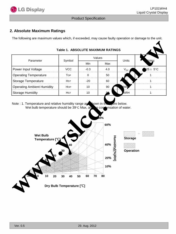
2. Absolute Maximum Ratings
The following are maximum values which, if exceeded, may cause faulty operation or damage to the unit.
Table 1. ABSOLUTE MAXIMUM RATINGS
Storage
Operation
10 20 30 40 50 60 70 800-20
Dry Bulb Temperature [℃]
10%
20%
40%
60%
90% 80%
010
20
30
40
50
60
Wet Bulb
Temperature [℃]
Hu
mid
ity[(%
)RH
]Parameter Symbol
ValuesUnits Notes
Min Max
Power Input Voltage VCC -0.3 4.0 VDC at 25 5C
Operating Temperature TOP 0 50 C 1
Storage Temperature HST -20 60 C 1
Operating Ambient Humidity HOP 10 90 %RH 1
Storage Humidity HST 10 90 %RH 1
Note : 1. Temperature and relative humidity range are shown in the figure below.
Wet bulb temperature should be 39C Max, and no condensation of water.
www.yslcd.com.tw
Product Specification
LP101WH4
Liquid Crystal Display
Ver. 0.5 29. Aug. 2012
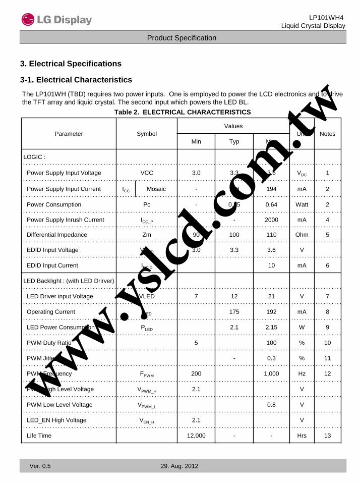
3. Electrical Specifications
3-1. Electrical Characteristics
Table 2. ELECTRICAL CHARACTERISTICS
Parameter Symbol
Values
Unit Notes
Min Typ Max
LOGIC :
Power Supply Input Voltage VCC 3.0 3.3 3.6 VDC 1
Power Supply Input Current ICC Mosaic - 166 194 mA 2
Power Consumption Pc - 0.55 0.64 Watt 2
Power Supply Inrush Current ICC_P - - 2000 mA 4
Differential Impedance Zm 90 100 110 Ohm 5
EDID Input Voltage VEDID 3.0 3.3 3.6 V
EDID Input Current IEDID 10 mA 6
LED Backlight : (with LED Drirver)
LED Driver input Voltage VLED 7 12 21 V 7
Operating Current ILED 175 192 mA 8
LED Power Consumption PLED 2.1 2.15 W 9
PWM Duty Ratio 5 100 % 10
PWM Jitter - 0.3 % 11
PWM Frequency FPWM 200 1,000 Hz 12
PWM High Level Voltage VPWM_H 2.1 V
PWM Low Level Voltage VPWM_L 0.8 V
LED_EN High Voltage VEN_H 2.1 V
Life Time 12,000 - - Hrs 13
The LP101WH (TBD) requires two power inputs. One is employed to power the LCD electronics and to drive
the TFT array and liquid crystal. The second input which powers the LED BL.
www.yslcd.com.tw
Product Specification
LP101WH4
Liquid Crystal Display
Ver. 0.5 29. Aug. 2012
Note)
1. The measuring position is the connector of LCM and the test conditions are under 25℃, fv = 60Hz,
Mosaic pattern.
2. The specified Icc current and power consumption are under
the Vcc = 3.3V , 25℃, fv = 60Hz condition whereas Mosaic pattern
is displayed and fv is the frame frequency.
3. This Spec. is the max load condition for the cable impedance designing.
4. The below figures are the measuring Vcc condition and the Vcc control block LGD used.
The Vcc condition is same the minimum of T1 at Power on sequence.
5. This impedance value is needed to proper display and measured form LVDS Tx to the mating connector.
6. The specified IEDID current are under the Vcc = 3.3V @ frequency = 330Khz condition.
7. The measuring position is the connector of LCM and the test conditions are under 25℃.
8. The current and power consumption with LED Driver are under the Vled = 12.0V , 25℃, Dimming of
Max luminance whereas White pattern is displayed and fv is the frame frequency.
9. The below figures are the measuring Vled condition
and the Vled control block LGD used.
VLED control block is same with Vcc control block.
10. The operation of LED Driver below minimum dimming ratio may cause F.O.S or reliability issue.
11. If Jitter of PWM is bigger than maximum. It may cause flickering.
12. This Spec. is not effective at 100% dimming ratio as an exception because it has DC level equivalent
to 0Hz. In spite of acceptable range as defined, the PWM Frequency should be fixed and stable for
more consistent brightness control at any specific level desired.
13. The life time is determined as the time at which the typical brightness of LCD is 50% compare to that of
initial value at the typical LED current.
10%
90%
0.5ms
3.3V
0V
Rising time
Vcc
10%
90%
0.5ms
12.0V
0V
Rising time
VLED
www.yslcd.com.tw
Product Specification
LP101WH4
Liquid Crystal Display
Ver. 0.5 29. Aug. 2012
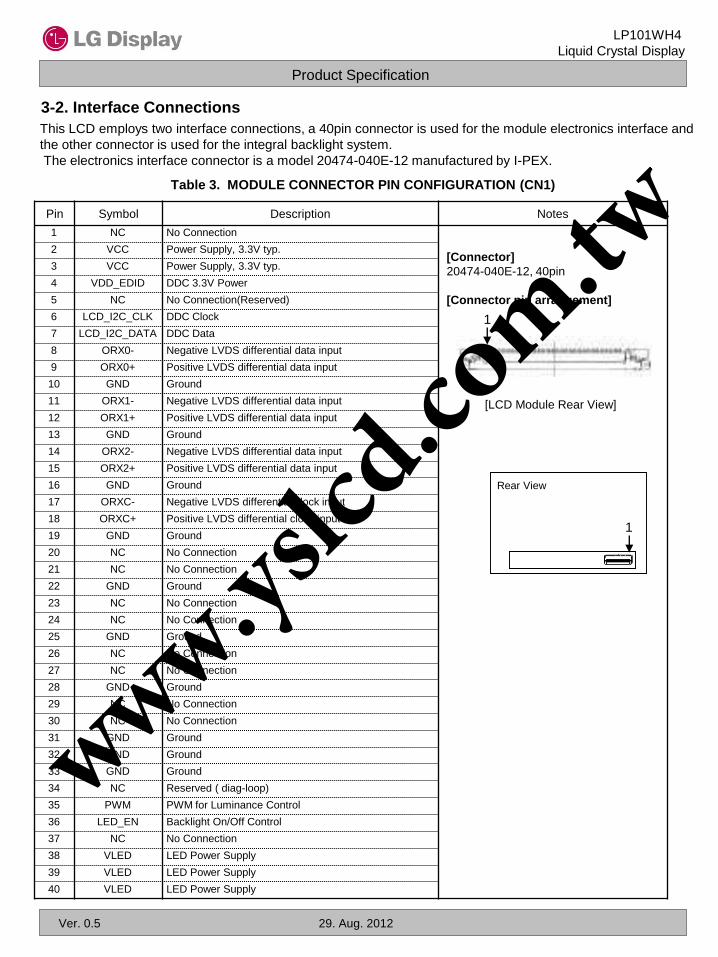
3-2. Interface Connections
This LCD employs two interface connections, a 40pin connector is used for the module electronics interface and
the other connector is used for the integral backlight system.
The electronics interface connector is a model 20474-040E-12 manufactured by I-PEX.
Table 3. MODULE CONNECTOR PIN CONFIGURATION (CN1)
Pin Symbol Description Notes
1 NC No Connection
2 VCC Power Supply, 3.3V typ.
3 VCC Power Supply, 3.3V typ.
4 VDD_EDID DDC 3.3V Power
5 NC No Connection(Reserved)
6 LCD_I2C_CLK DDC Clock
7 LCD_I2C_DATA DDC Data
8 ORX0- Negative LVDS differential data input
9 ORX0+ Positive LVDS differential data input
10 GND Ground
11 ORX1- Negative LVDS differential data input
12 ORX1+ Positive LVDS differential data input
13 GND Ground
14 ORX2- Negative LVDS differential data input
15 ORX2+ Positive LVDS differential data input
16 GND Ground
17 ORXC- Negative LVDS differential clock input
18 ORXC+ Positive LVDS differential clock input
19 GND Ground
20 NC No Connection
21 NC No Connection
22 GND Ground
23 NC No Connection
24 NC No Connection
25 GND Ground
26 NC No Connection
27 NC No Connection
28 GND Ground
29 NC No Connection
30 NC No Connection
31 GND Ground
32 GND Ground
33 GND Ground
34 NC Reserved ( diag-loop)
35 PWM PWM for Luminance Control
36 LED_EN Backlight On/Off Control
37 NC No Connection
38 VLED LED Power Supply
39 VLED LED Power Supply
40 VLED LED Power Supply
[Connector]
20474-040E-12, 40pin
[Connector pin arrangement]
[LCD Module Rear View]
Rear View
1
1
www.yslcd.com.tw
Product Specification
LP101WH4
Liquid Crystal Display
Ver. 0.5 29. Aug. 2012
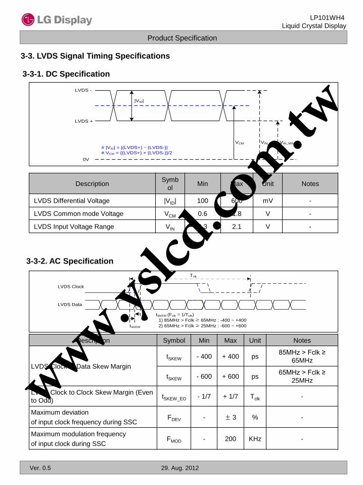
3-3-1. DC Specification
3-3. LVDS Signal Timing Specifications
Description Symbol Min Max Unit Notes
LVDS Clock to Data Skew Margin
tSKEW - 400 + 400 ps85MHz > Fclk ≥
65MHz
tSKEW - 600 + 600 ps65MHz > Fclk ≥
25MHz
LVDS Clock to Clock Skew Margin (Even
to Odd)tSKEW_EO - 1/7 + 1/7 Tclk -
Maximum deviation
of input clock frequency during SSCFDEV - ± 3 % -
Maximum modulation frequency
of input clock during SSCFMOD - 200 KHz -
DescriptionSymb
olMin Max Unit Notes
LVDS Differential Voltage |VID| 100 600 mV -
LVDS Common mode Voltage VCM 0.6 1.8 V -
LVDS Input Voltage Range VIN 0.3 2.1 V -
3-3-2. AC Specification
LVDS +
LVDS -
0V
VCM
# |VID| = |(LVDS+) – (LVDS-)|
# VCM = {(LVDS+) + (LVDS-)}/2
|VID|
VIN_MAX VIN_MIN
LVDS Data
tSKEW
LVDS Clock
Tclk
tSKEW (Fclk = 1/Tclk)
1) 85MHz > Fclk ≥ 65MHz : -400 ~ +400
2) 65MHz > Fclk ≥ 25MHz : -600 ~ +600
www.yslcd.com.tw
Product Specification
LP101WH4
Liquid Crystal Display
Ver. 0.5 29. Aug. 2012
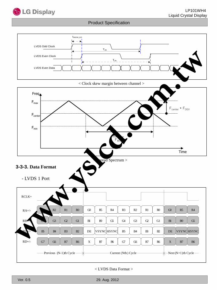
LVDS Even Data
LVDS Odd Clock
LVDS Even Clock
tSKEW_EO
Tclk
Tclk
< Clock skew margin between channel >
< LVDS Data Format >
3-3-3. Data Format
- LVDS 1 Port
< Spread Spectrum >
Time
Fcenter
Fmax
Fmin
FMOD
1
Fcenter * FDEV
Freq.
G0 R5 R4 R3 R2 R1 R0
B1 B0 G5 G4 G3 G2 G1
DE VSYNC HSYNC B5 B4 B3 B2
X B7 B6 G7 G6 R7 R6
R1 R0
G2 G1
B3 B2
R7 R6
G0
B1
DE
X
Current (Nth ) Cycle
R5 R4
B0 G5
VSYNC HSYNC
B7 B6
R3 R2
G4 G3
B5 B4
G7 G6
Previous (N-1)th Cycle Next (N+1)th Cycle
RCLK+
RA+/-
RB+/-
RC+/-
RD+/-www.yslcd.com.tw
Product Specification
LP101WH4
Liquid Crystal Display
Ver. 0.5 29. Aug. 2012
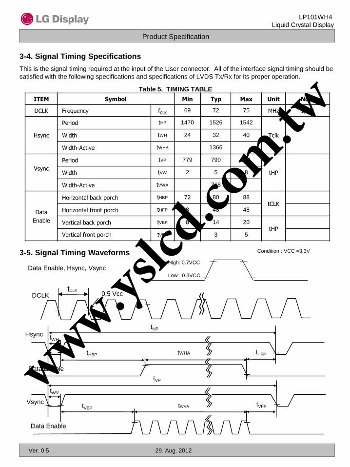
3-4. Signal Timing Specifications
Table 5. TIMING TABLE
This is the signal timing required at the input of the User connector. All of the interface signal timing should be
satisfied with the following specifications and specifications of LVDS Tx/Rx for its proper operation.
3-5. Signal Timing Waveforms Condition : VCC =3.3V
Low: 0.3VCC
High: 0.7VCCData Enable, Hsync, Vsync
Hsync
Data Enable
Vsync
Data Enable
tWH
tHP
tHFPtHBP
tVP
tWV
tVBPtVFP
tWHA
tWVA
tCLK0.5 VccDCLK
ITEM Symbol Min Typ Max Unit Note
DCLK Frequency fCLK 69 72 75 MHz 1port
Hsync
Period tHP 1470 1526 1542
TclkWidth tWH 24 32 40
Width-Active tWHA 1366
Vsync
Period tVP 779 790 801
tHPWidth tVW 2 5 8
Width-Active tVWA 768
Data
Enable
Horizontal back porch tHBP 72 80 88tCLK
Horizontal front porch tHFP 8 48 48
Vertical back porch tVBP 8 14 20tHP
Vertical front porch tVFP 1 3 5
www.yslcd.com.tw
Product Specification
LP101WH4
Liquid Crystal Display
Ver. 0.5 29. Aug. 2012
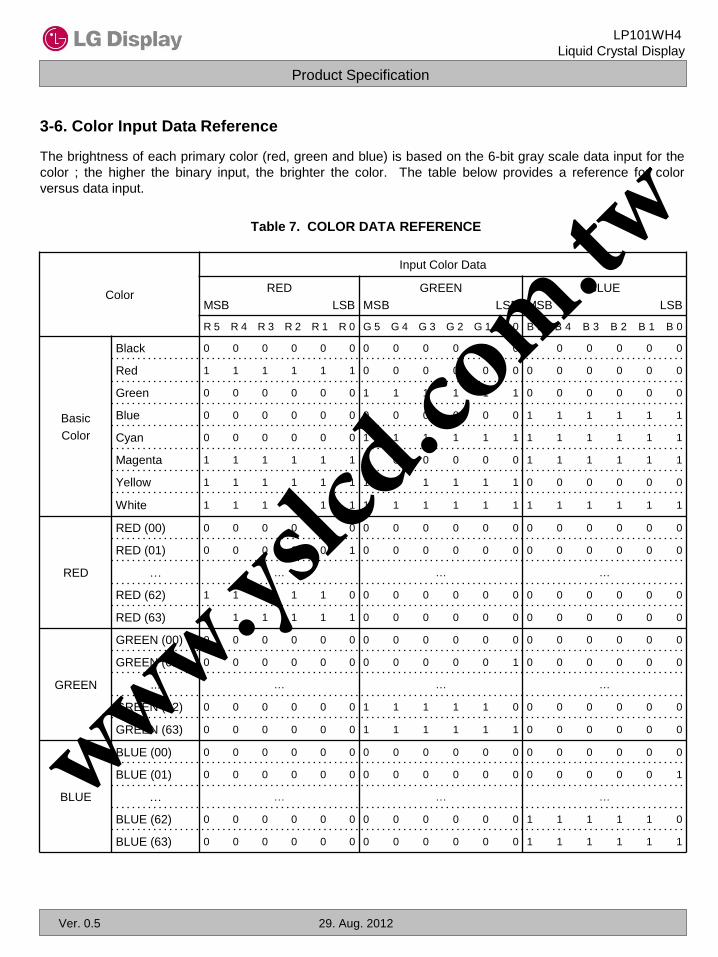
3-6. Color Input Data Reference
The brightness of each primary color (red, green and blue) is based on the 6-bit gray scale data input for the
color ; the higher the binary input, the brighter the color. The table below provides a reference for color
versus data input.
Table 7. COLOR DATA REFERENCE
Color
Input Color Data
RED
MSB LSB
GREEN
MSB LSB
BLUE
MSB LSB
R 5 R 4 R 3 R 2 R 1 R 0 G 5 G 4 G 3 G 2 G 1 G 0 B 5 B 4 B 3 B 2 B 1 B 0
Basic
Color
Black 0 0 0 0 0 0 0 0 0 0 0 0 0 0 0 0 0 0
Red 1 1 1 1 1 1 0 0 0 0 0 0 0 0 0 0 0 0
Green 0 0 0 0 0 0 1 1 1 1 1 1 0 0 0 0 0 0
Blue 0 0 0 0 0 0 0 0 0 0 0 0 1 1 1 1 1 1
Cyan 0 0 0 0 0 0 1 1 1 1 1 1 1 1 1 1 1 1
Magenta 1 1 1 1 1 1 0 0 0 0 0 0 1 1 1 1 1 1
Yellow 1 1 1 1 1 1 1 1 1 1 1 1 0 0 0 0 0 0
White 1 1 1 1 1 1 1 1 1 1 1 1 1 1 1 1 1 1
RED
RED (00) 0 0 0 0 0 0 0 0 0 0 0 0 0 0 0 0 0 0
RED (01) 0 0 0 0 0 1 0 0 0 0 0 0 0 0 0 0 0 0
… … … …
RED (62) 1 1 1 1 1 0 0 0 0 0 0 0 0 0 0 0 0 0
RED (63) 1 1 1 1 1 1 0 0 0 0 0 0 0 0 0 0 0 0
GREEN
GREEN (00) 0 0 0 0 0 0 0 0 0 0 0 0 0 0 0 0 0 0
GREEN (01) 0 0 0 0 0 0 0 0 0 0 0 1 0 0 0 0 0 0
... … … …
GREEN (62) 0 0 0 0 0 0 1 1 1 1 1 0 0 0 0 0 0 0
GREEN (63) 0 0 0 0 0 0 1 1 1 1 1 1 0 0 0 0 0 0
BLUE
BLUE (00) 0 0 0 0 0 0 0 0 0 0 0 0 0 0 0 0 0 0
BLUE (01) 0 0 0 0 0 0 0 0 0 0 0 0 0 0 0 0 0 1
… … … …
BLUE (62) 0 0 0 0 0 0 0 0 0 0 0 0 1 1 1 1 1 0
BLUE (63) 0 0 0 0 0 0 0 0 0 0 0 0 1 1 1 1 1 1
www.yslcd.com.tw
Product Specification
LP101WH4
Liquid Crystal Display
Ver. 0.5 29. Aug. 2012
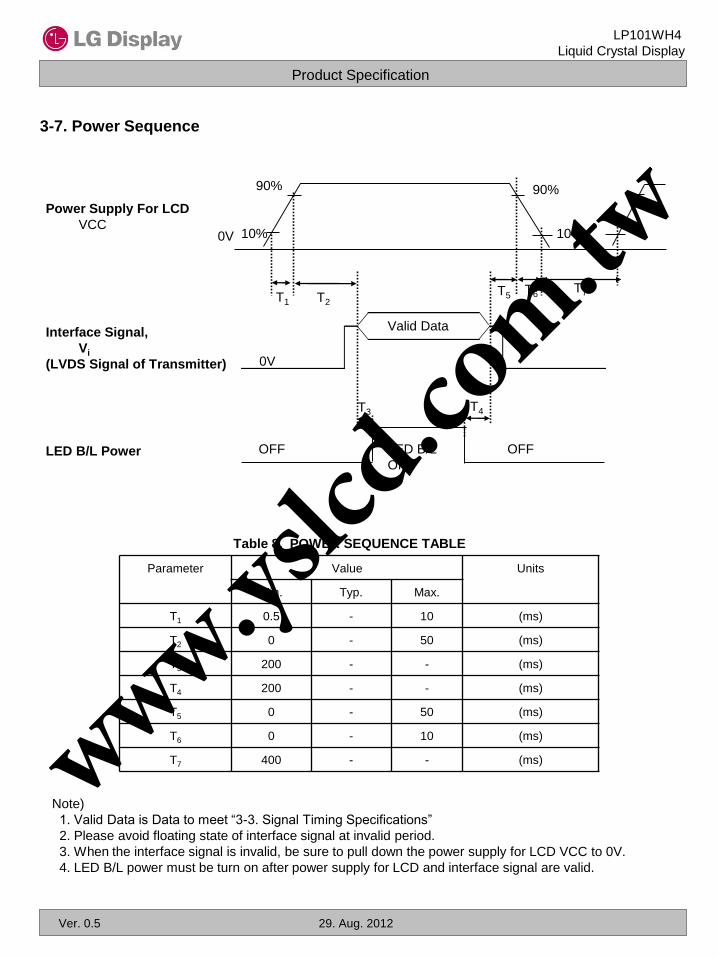
3-7. Power Sequence
Note)
1. Valid Data is Data to meet “3-3. Signal Timing Specifications”
2. Please avoid floating state of interface signal at invalid period.
3. When the interface signal is invalid, be sure to pull down the power supply for LCD VCC to 0V.
4. LED B/L power must be turn on after power supply for LCD and interface signal are valid.
Parameter Value Units
Min. Typ. Max.
T1 0.5 - 10 (ms)
T2 0 - 50 (ms)
T3 200 - - (ms)
T4 200 - - (ms)
T5 0 - 50 (ms)
T6 0 - 10 (ms)
T7 400 - - (ms)
Table 8. POWER SEQUENCE TABLE
T6
Interface Signal,
Vi
(LVDS Signal of Transmitter)
LED B/L Power
Power Supply For LCD
VCC
90%
10%10%0V
90%
T1 T2T5
Valid Data
0V
OFFOFF LED B/L
ON
T7
T3 T4
www.yslcd.com.tw
Product Specification
LP101WH4
Liquid Crystal Display
Ver. 0.5 29. Aug. 2012
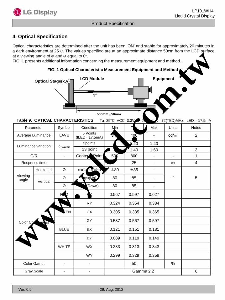
4. Optical Specification
FIG. 1 Optical Characteristic Measurement Equipment and Method
Table 9. OPTICAL CHARACTERISTICS
Optical characteristics are determined after the unit has been ‘ON’ and stable for approximately 20 minutes in
a dark environment at 25C. The values specified are at an approximate distance 50cm from the LCD surface
at a viewing angle of and equal to 0.
FIG. 1 presents additional information concerning the measurement equipment and method.
Ta=25C, VCC=3.3V, fV=60Hz, fCLK= 72(TBD)MHz, ILED = 17.5mA
Parameter Symbol Condition Min Typ Max Units Notes
Average Luminance LAVE5 Points
(ILED= 17.5mA)340 400 - cd/㎡ 2
Luminance variation WHITE
5points - 1.20 1.40
13 point - 1.40 1.60 3
C/R - Center 1 Point 500 800 - - 1
Response time - - 25 - ㎳ 4
Viewingangle
Horizontal Θ φx(Left,Right) ± 80 ± 85 -
˚ 5Vertical
Θ φyu(Up) 80 85 -
Θ φyd(Down) 80 85 -
Color Coordinates
RED RX 0.567 0.597 0.627
RY 0.324 0.354 0.384
GREEN GX 0.305 0.335 0.365
GY 0.537 0.567 0.597
BLUE BX 0.121 0.151 0.181
BY 0.089 0.119 0.149
WHITE WX 0.283 0.313 0.343
WY 0.299 0.329 0.359
Color Gamut - - 50 %
Gray Scale - - Gamma 2.2 6
LCD ModuleOptical Stage(x,y)
Equipment
500mm± 50mm
www.yslcd.com.tw
Product Specification
LP101WH4
Liquid Crystal Display
Ver. 0.5 29. Aug. 2012
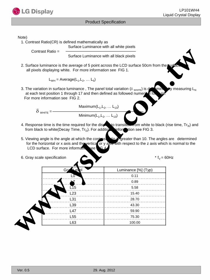
Note)
1. Contrast Ratio(CR) is defined mathematically as
Surface Luminance with all white pixels
Contrast Ratio =
Surface Luminance with all black pixels
2. Surface luminance is the average of 5 point across the LCD surface 50cm from the surface with
all pixels displaying white. For more information see FIG 1.
LWH = Average(L1,L2, … L5)
3. The variation in surface luminance , The panel total variation ( WHITE) is determined by measuring LN
at each test position 1 through 17 and then defined as followed numerical formula.
For more information see FIG 2.
Maximum(L1,L2, … L13)
WHITE =Minimum(L1,L2, … L13)
4. Response time is the time required for the display to transition from white to black (rise time, TrR) and
from black to white(Decay Time, TrD). For additional information see FIG 3.
5. Viewing angle is the angle at which the contrast ratio is greater than 10. The angles are determined
for the horizontal or x axis and the vertical or y axis with respect to the z axis which is normal to the
LCD surface. For more information see FIG 4.
6. Gray scale specification * fV = 60Hz
Gray Level Luminance [%] (Typ)
L0 0.11
L7 0.89
L15 5.58
L23 15.40
L31 28.70
L39 43.30
L47 59.90
L55 75.30
L63 100.00www.yslcd.com.tw
Product Specification
LP101WH4
Liquid Crystal Display
Ver. 0.5 29. Aug. 2012
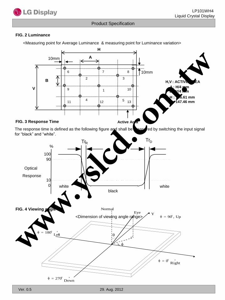
FIG. 4 Viewing angle
<Dimension of viewing angle range>
Normal
YEye
= 0,
Right
= 180,
Left
= 270,
Down
= 90, Up
FIG. 3 Response Time
The response time is defined as the following figure and shall be measured by switching the input signal
for “black” and “white”.
TrRTrD
100
90
10
0
%
Optical
Response
whiteblack
white
FIG. 2 Luminance
<Measuring point for Average Luminance & measuring point for Luminance variation>
: ACTIVE AREA
A : H/4 mmB : V/4 mm
H : 196.61 mm
V : 147.46 mm
H,V
Active Area
1
32
54
H
A
B
V
6 7 8
9 10
11 12 13
10mm
10mm
www.yslcd.com.tw
Product Specification
LP101WH4
Liquid Crystal Display
Ver. 0.5 29. Aug. 2012
5. Mechanical Characteristics
The contents provide general mechanical characteristics for the model LP101WH (TBD). In addition the
figures in the next page are detailed mechanical drawing of the LCD.
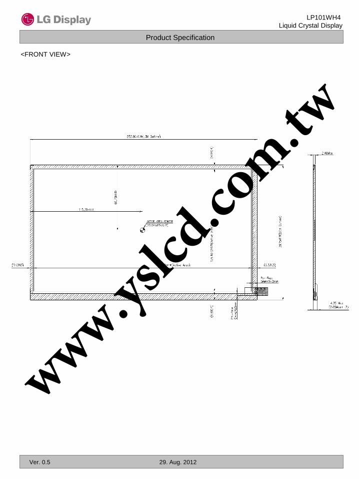
Outline Dimension
Horizontal 232.8 0.3mm (without bracket length)
Vertical 138.15 0.3mm (without bracket length)
Thickness 2.40mm (max.)
Bezel AreaHorizontal TBD
Vertical TBD
Active Display AreaHorizontal 222.5214mm
Vertical 125.1072mm
Weight 125g (Max.) w/o Touch
Surface Treatment LCD : Glare, low reflective treatment of the front polarizer, 2H
www.yslcd.com.tw
Product Specification
LP101WH4
Liquid Crystal Display
Ver. 0.5 29. Aug. 2012
<FRONT VIEW>
www.yslcd.com.tw
Product Specification
LP101WH4
Liquid Crystal Display
Ver. 0.5 29. Aug. 2012
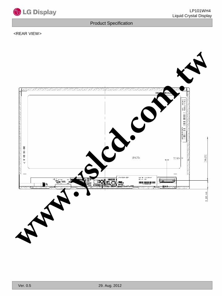
<REAR VIEW>
www.yslcd.com.tw
Product Specification
LP101WH4
Liquid Crystal Display
Ver. 0.5 29. Aug. 2012
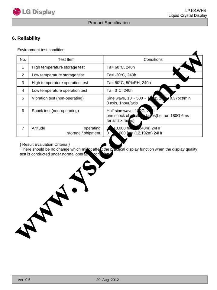
6. Reliability
Environment test condition
{ Result Evaluation Criteria }
There should be no change which might affect the practical display function when the display quality
test is conducted under normal operating condition.
No. Test Item Conditions
1 High temperature storage test Ta= 60C, 240h
2 Low temperature storage test Ta= -20C, 240h
3 High temperature operation test Ta= 50C, 50%RH, 240h
4 Low temperature operation test Ta= 0C, 240h
5 Vibration test (non-operating) Sine wave, 10 ~ 500 ~ 10Hz, 1.5G, 0.37oct/min
3 axis, 1hour/axis
6 Shock test (non-operating) Half sine wave, 180G, 2ms
one shock of each six faces(I.e. run 180G 6ms
for all six faces)
7 Altitude operating
storage / shipment
0 ~ 10,000 feet (3,048m) 24Hr
0 ~ 40,000 feet (12,192m) 24Hr
www.yslcd.com.tw
Product Specification
LP101WH4
Liquid Crystal Display
Ver. 0.5 29. Aug. 2012
7. International Standards
7-2. EMC
a) ANSI C63.4 “Methods of Measurement of Radio-Noise Emissions from Low-Voltage Electrical and
Electrical Equipment in the Range of 9kHZ to 40GHz. “American National Standards Institute(ANSI),
1992
b) C.I.S.P.R “Limits and Methods of Measurement of Radio Interface Characteristics of Information
Technology Equipment.“ International Special Committee on Radio Interference.
c) EN 55022 “Limits and Methods of Measurement of Radio Interface Characteristics of Information
Technology Equipment.“ European Committee for Electrotechnical Standardization.(CENELEC), 1998
( Including A1: 2000 )
7-1. Safety
c) EN 60950-1, European Committee for Electrotechnical Standardization (CENELEC).
Information Technology Equipment - Safety - Part 1 : General Requirements.
a) UL 60950-1, Underwriters Laboratories Inc.
Information Technology Equipment - Safety - Part 1 : General Requirements.
b) CAN/CSA C22.2 No.60950-1-07, Canadian Standards Association.
Information Technology Equipment - Safety - Part 1 : General Requirements.
d) IEC 60950-1, The International Electrotechnical Commission (IEC).
Information Technology Equipment - Safety - Part 1 : General Requirements.
www.yslcd.com.tw
Product Specification
LP101WH4
Liquid Crystal Display
Ver. 0.5 29. Aug. 2012
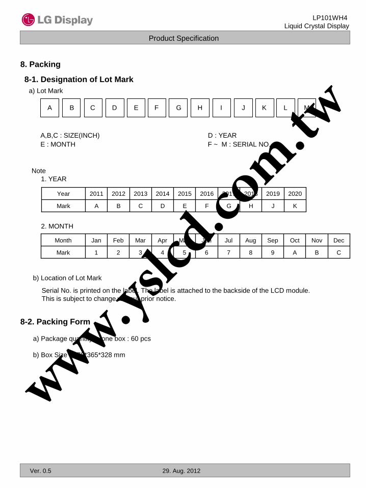
8. Packing
8-2. Packing Form
8-1. Designation of Lot Mark
a) Lot Mark
A B C D E F G H I J K L M
A,B,C : SIZE(INCH) D : YEAR
E : MONTH F ~ M : SERIAL NO.
Note
1. YEAR
2. MONTH
B
Nov
Mark
Month
A
Oct
6
Jun
7
Jul
8
Aug
9
Sep
4
Apr
5
May
C321
DecMarFebJan
b) Location of Lot Mark
Serial No. is printed on the label. The label is attached to the backside of the LCD module.
This is subject to change without prior notice.
Mark
Year
K
2020
F
2016
G
2017
H
2018
J
2019
D
2014
E
2015
CBA
201320122011
a) Package quantity in one box : 60 pcs
b) Box Size : 478*365*328 mm
www.yslcd.com.tw
Product Specification
LP101WH4
Liquid Crystal Display
Ver. 0.5 29. Aug. 2012
9. PRECAUTIONS
Please pay attention to the followings when you use this TFT LCD module.
9-1. MOUNTING PRECAUTIONS
(1) You must mount a module using holes arranged in four corners or four sides.
(2) You should consider the mounting structure so that uneven force (ex. Twisted stress) is not applied to the
module. And the case on which a module is mounted should have sufficient strength so that external
force is not transmitted directly to the module.
(3) Please attach the surface transparent protective plate to the surface in order to protect the polarizer.
Transparent protective plate should have sufficient strength in order to the resist external force.
(4) You should adopt radiation structure to satisfy the temperature specification.
(5) Acetic acid type and chlorine type materials for the cover case are not desirable because the former
generates corrosive gas of attacking the polarizer at high temperature and the latter causes circuit break
by electro-chemical reaction.
(6) Do not touch, push or rub the exposed polarizers with glass, tweezers or anything harder than HB
pencil lead. And please do not rub with dust clothes with chemical treatment.
Do not touch the surface of polarizer for bare hand or greasy cloth.(Some cosmetics are detrimental
to the polarizer.)
(7) When the surface becomes dusty, please wipe gently with absorbent cotton or other soft materials like
chamois soaks with petroleum benzene. Normal-hexane is recommended for cleaning the adhesives
used to attach front / rear polarizers. Do not use acetone, toluene and alcohol because they cause
chemical damage to the polarizer.
(8) Wipe off saliva or water drops as soon as possible. Their long time contact with polarizer causes
deformations and color fading.
(9) Do not open the case because inside circuits do not have sufficient strength.
9-2. OPERATING PRECAUTIONS
(1) The spike noise causes the mis-operation of circuits. It should be lower than following voltage :
V=± 200mV(Over and under shoot voltage)
(2) Response time depends on the temperature.(In lower temperature, it becomes longer.)
(3) Brightness depends on the temperature. (In lower temperature, it becomes lower.)
And in lower temperature, response time(required time that brightness is stable after turned on) becomes
longer.
(4) Be careful for condensation at sudden temperature change. Condensation makes damage to polarizer or
electrical contacted parts. And after fading condensation, smear or spot will occur.
(5) When fixed patterns are displayed for a long time, remnant image is likely to occur.
(6) Module has high frequency circuits. Sufficient suppression to the electromagnetic interference shall be
done by system manufacturers. Grounding and shielding methods may be important to minimized the
interference.
www.yslcd.com.tw
Product Specification
LP101WH4
Liquid Crystal Display
Ver. 0.5 29. Aug. 2012
Since a module is composed of electronic circuits, it is not strong to electrostatic discharge. Make certain that
treatment persons are connected to ground through wrist band etc. And don’t touch interface pin directly.
9-3. ELECTROSTATIC DISCHARGE CONTROL
Strong light exposure causes degradation of polarizer and color filter.
9-4. PRECAUTIONS FOR STRONG LIGHT EXPOSURE
9-5. STORAGE
(1) When the protection film is peeled off, static electricity is generated between the film and polarizer.
This should be peeled off slowly and carefully by people who are electrically grounded and with well
ion-blown equipment or in such a condition, etc.
(2) The protection film is attached to the polarizer with a small amount of glue. If some stress is applied
to rub the protection film against the polarizer during the time you peel off the film, the glue is apt to
remain on the polarizer.
Please carefully peel off the protection film without rubbing it against the polarizer.
(3) When the module with protection film attached is stored for a long time, sometimes there remains a
very small amount of glue still on the polarizer after the protection film is peeled off.
(4) You can remove the glue easily. When the glue remains on the polarizer surface or its vestige is
recognized, please wipe them off with absorbent cotton waste or other soft material like chamois
soaked with normal-hexane.
9-6. HANDLING PRECAUTIONS FOR PROTECTION FILM
When storing modules as spares for a long time, the following precautions are necessary.
(1) Store them in a dark place. Do not expose the module to sunlight or fluorescent light. Keep the
temperature between 5C and 35C at normal humidity.
(2) The polarizer surface should not come in contact with any other object.
It is recommended that they be stored in the container in which they were shipped.
www.yslcd.com.tw
Product Specification
LP101WH4
Liquid Crystal Display
Ver. 0.5 29. Aug. 2012
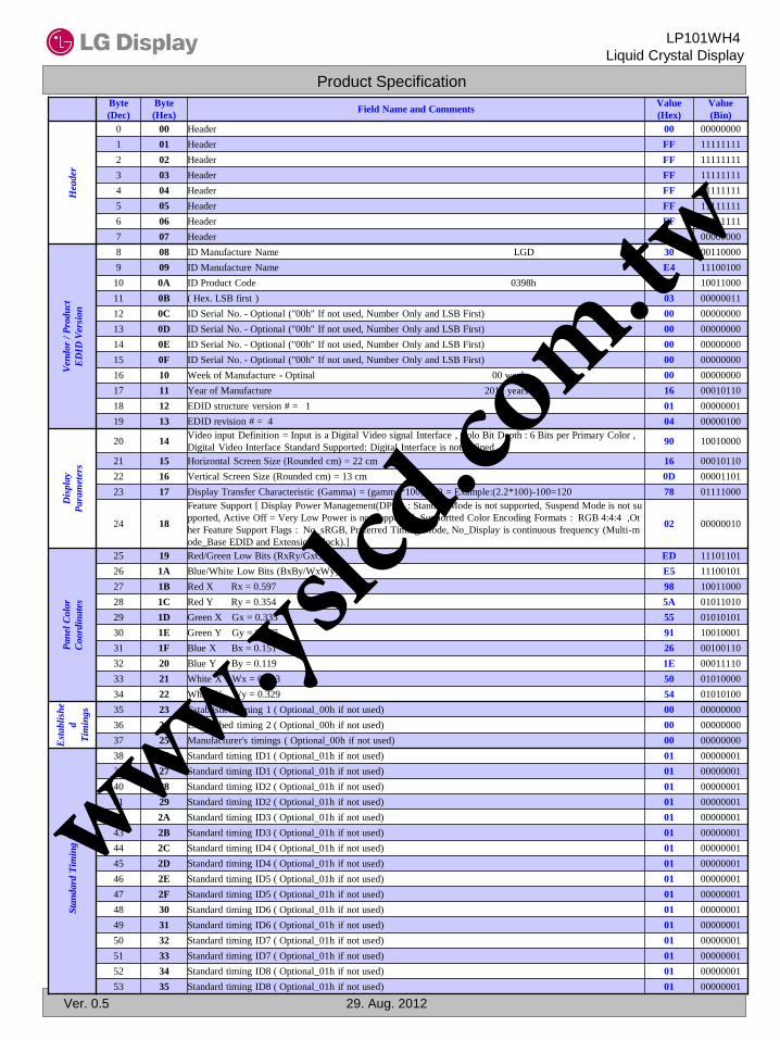
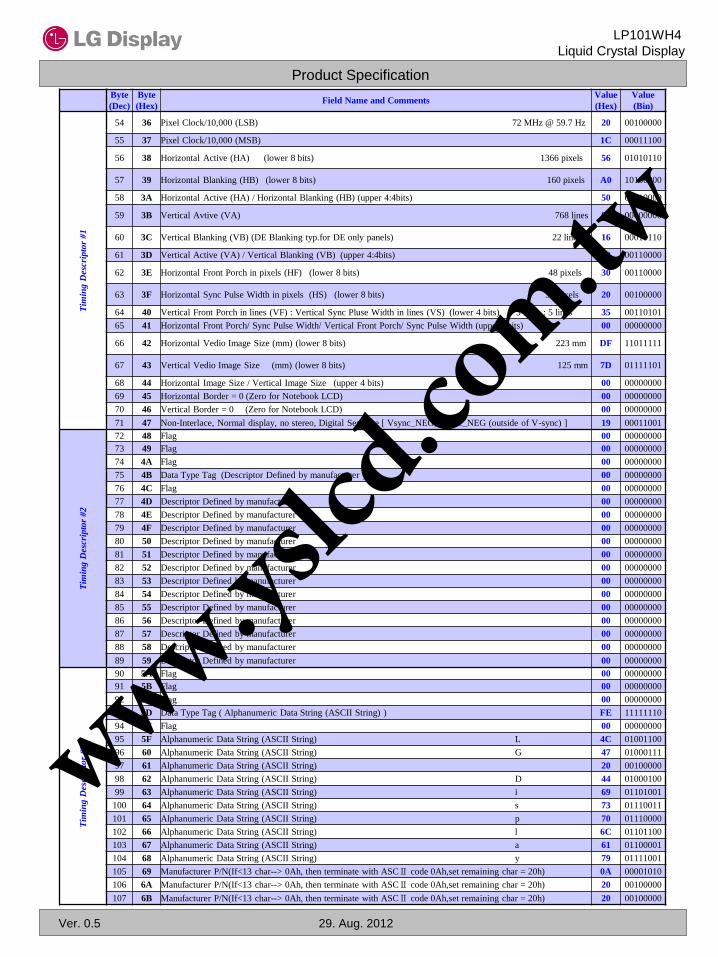
Byte
(Dec)
Byte
(Hex)Field Name and Comments
Value
(Hex)
Value
(Bin)
Hea
der
0 00 Header 00 00000000
1 01 Header FF 11111111
2 02 Header FF 11111111
3 03 Header FF 11111111
4 04 Header FF 11111111
5 05 Header FF 11111111
6 06 Header FF 11111111
7 07 Header 00 00000000
Ven
do
r /
Pro
du
ct
ED
ID V
ersi
on
8 08 ID Manufacture Name LGD 30 00110000
9 09 ID Manufacture Name E4 11100100
10 0A ID Product Code 0398h 98 10011000
11 0B ( Hex. LSB first ) 03 00000011
12 0C ID Serial No. - Optional ("00h" If not used, Number Only and LSB First) 00 00000000
13 0D ID Serial No. - Optional ("00h" If not used, Number Only and LSB First) 00 00000000
14 0E ID Serial No. - Optional ("00h" If not used, Number Only and LSB First) 00 00000000
15 0F ID Serial No. - Optional ("00h" If not used, Number Only and LSB First) 00 00000000
16 10 Week of Manufacture - Optinal 00 weeks 00 00000000
17 11 Year of Manufacture 2012 years 16 00010110
18 12 EDID structure version # = 1 01 00000001
19 13 EDID revision # = 4 04 00000100
Dis
pla
y
Pa
ram
eter
s
20 14Video input Definition = Input is a Digital Video signal Interface , Colo Bit Depth : 6 Bits per Primary Color ,
Digital Video Interface Standard Supported: Digital Interface is not defined90 10010000
21 15 Horizontal Screen Size (Rounded cm) = 22 cm 16 00010110
22 16 Vertical Screen Size (Rounded cm) = 13 cm 0D 00001101
23 17 Display Transfer Characteristic (Gamma) = (gamma*100)-100 = Example:(2.2*100)-100=120 78 01111000
24 18
Feature Support [ Display Power Management(DPM) : Standby Mode is not supported, Suspend Mode is not su
pported, Active Off = Very Low Power is not supported ,Supportted Color Encoding Formats : RGB 4:4:4 ,Ot
her Feature Support Flags : No_sRGB, Preferred Timing Mode, No_Display is continuous frequency (Multi-m
ode_Base EDID and Extension Block).]
02 00000010
Pa
nel
Co
lor
Co
ord
ina
tes
25 19 Red/Green Low Bits (RxRy/GxGy) ED 11101101
26 1A Blue/White Low Bits (BxBy/WxWy) E5 11100101
27 1B Red X Rx = 0.597 98 10011000
28 1C Red Y Ry = 0.354 5A 01011010
29 1D Green X Gx = 0.335 55 01010101
30 1E Green Y Gy = 0.567 91 10010001
31 1F Blue X Bx = 0.151 26 00100110
32 20 Blue Y By = 0.119 1E 00011110
33 21 White X Wx = 0.313 50 01010000
34 22 White Y Wy = 0.329 54 01010100
Est
abli
she
d
Tim
ing
s 35 23 Established timing 1 ( Optional_00h if not used) 00 00000000
36 24 Established timing 2 ( Optional_00h if not used) 00 00000000
37 25 Manufacturer's timings ( Optional_00h if not used) 00 00000000
Sta
nd
ard
Tim
ing I
D
38 26 Standard timing ID1 ( Optional_01h if not used) 01 00000001
39 27 Standard timing ID1 ( Optional_01h if not used) 01 00000001
40 28 Standard timing ID2 ( Optional_01h if not used) 01 00000001
41 29 Standard timing ID2 ( Optional_01h if not used) 01 00000001
42 2A Standard timing ID3 ( Optional_01h if not used) 01 00000001
43 2B Standard timing ID3 ( Optional_01h if not used) 01 00000001
44 2C Standard timing ID4 ( Optional_01h if not used) 01 00000001
45 2D Standard timing ID4 ( Optional_01h if not used) 01 00000001
46 2E Standard timing ID5 ( Optional_01h if not used) 01 00000001
47 2F Standard timing ID5 ( Optional_01h if not used) 01 00000001
48 30 Standard timing ID6 ( Optional_01h if not used) 01 00000001
49 31 Standard timing ID6 ( Optional_01h if not used) 01 00000001
50 32 Standard timing ID7 ( Optional_01h if not used) 01 00000001
51 33 Standard timing ID7 ( Optional_01h if not used) 01 00000001
52 34 Standard timing ID8 ( Optional_01h if not used) 01 00000001
53 35 Standard timing ID8 ( Optional_01h if not used) 01 00000001
www.yslcd.com.tw
Product Specification
LP101WH4
Liquid Crystal Display
Ver. 0.5 29. Aug. 2012
Byte
(Dec)
Byte
(Hex)Field Name and Comments
Value
(Hex)
Value
(Bin)
Tim
ing
Desc
ripto
r #1
54 36 Pixel Clock/10,000 (LSB) 72 MHz @ 59.7 Hz 20 00100000
55 37 Pixel Clock/10,000 (MSB) 1C 00011100
56 38 Horizontal Active (HA) (lower 8 bits) 1366 pixels 56 01010110
57 39 Horizontal Blanking (HB) (lower 8 bits) 160 pixels A0 10100000
58 3A Horizontal Active (HA) / Horizontal Blanking (HB) (upper 4:4bits) 50 01010000
59 3B Vertical Avtive (VA) 768 lines 00 00000000
60 3C Vertical Blanking (VB) (DE Blanking typ.for DE only panels) 22 lines 16 00010110
61 3D Vertical Active (VA) / Vertical Blanking (VB) (upper 4:4bits) 30 00110000
62 3E Horizontal Front Porch in pixels (HF) (lower 8 bits) 48 pixels 30 00110000
63 3F Horizontal Sync Pulse Width in pixels (HS) (lower 8 bits) 32 pixels 20 00100000
64 40 Vertical Front Porch in lines (VF) : Vertical Sync Pluse Width in lines (VS) (lower 4 bits) 3 lines : 5 lines 35 00110101
65 41 Horizontal Front Porch/ Sync Pulse Width/ Vertical Front Porch/ Sync Pulse Width (upper 2bits) 00 00000000
66 42 Horizontal Vedio Image Size (mm) (lower 8 bits) 223 mm DF 11011111
67 43 Vertical Vedio Image Size (mm) (lower 8 bits) 125 mm 7D 01111101
68 44 Horizontal Image Size / Vertical Image Size (upper 4 bits) 00 00000000
69 45 Horizontal Border = 0 (Zero for Notebook LCD) 00 00000000
70 46 Vertical Border = 0 (Zero for Notebook LCD) 00 00000000
71 47 Non-Interlace, Normal display, no stereo, Digital Separate [ Vsync_NEG, Hsync_NEG (outside of V-sync) ] 19 00011001
Tim
ing
Desc
rip
tor
#2
72 48 Flag 00 00000000
73 49 Flag 00 00000000
74 4A Flag 00 00000000
75 4B Data Type Tag (Descriptor Defined by manufacturer ) 00 00000000
76 4C Flag 00 00000000
77 4D Descriptor Defined by manufacturer 00 00000000
78 4E Descriptor Defined by manufacturer 00 00000000
79 4F Descriptor Defined by manufacturer 00 00000000
80 50 Descriptor Defined by manufacturer 00 00000000
81 51 Descriptor Defined by manufacturer 00 00000000
82 52 Descriptor Defined by manufacturer 00 00000000
83 53 Descriptor Defined by manufacturer 00 00000000
84 54 Descriptor Defined by manufacturer 00 00000000
85 55 Descriptor Defined by manufacturer 00 00000000
86 56 Descriptor Defined by manufacturer 00 00000000
87 57 Descriptor Defined by manufacturer 00 00000000
88 58 Descriptor Defined by manufacturer 00 00000000
89 59 Descriptor Defined by manufacturer 00 00000000
Tim
ing
Desc
ripto
r #3
90 5A Flag 00 00000000
91 5B Flag 00 00000000
92 5C Flag 00 00000000
93 5D Data Type Tag ( Alphanumeric Data String (ASCII String) ) FE 11111110
94 5E Flag 00 00000000
95 5F Alphanumeric Data String (ASCII String) L 4C 01001100
96 60 Alphanumeric Data String (ASCII String) G 47 01000111
97 61 Alphanumeric Data String (ASCII String) 20 00100000
98 62 Alphanumeric Data String (ASCII String) D 44 01000100
99 63 Alphanumeric Data String (ASCII String) i 69 01101001
100 64 Alphanumeric Data String (ASCII String) s 73 01110011
101 65 Alphanumeric Data String (ASCII String) p 70 01110000
102 66 Alphanumeric Data String (ASCII String) l 6C 01101100
103 67 Alphanumeric Data String (ASCII String) a 61 01100001
104 68 Alphanumeric Data String (ASCII String) y 79 01111001
105 69 Manufacturer P/N(If<13 char--> 0Ah, then terminate with ASCⅡ code 0Ah,set remaining char = 20h) 0A 00001010
106 6A Manufacturer P/N(If<13 char--> 0Ah, then terminate with ASCⅡ code 0Ah,set remaining char = 20h) 20 00100000
107 6B Manufacturer P/N(If<13 char--> 0Ah, then terminate with ASCⅡ code 0Ah,set remaining char = 20h) 20 00100000
www.yslcd.com.tw
Product Specification
LP101WH4
Liquid Crystal Display
Ver. 0.5 29. Aug. 2012
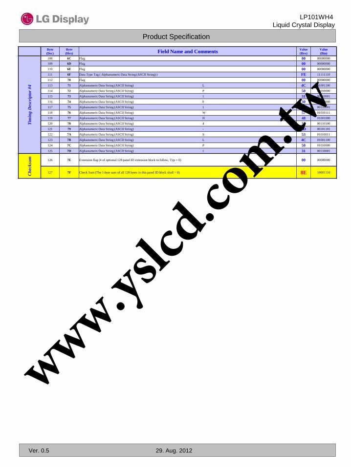
Byte
(Dec)
Byte
(Hex) Field Name and CommentsValue
(Hex)
Value
(Bin)
Tim
ing D
esc
ripto
r #4
108 6C Flag 00 00000000
109 6D Flag 00 00000000
110 6E Flag 00 00000000
111 6F Data Type Tag ( Alphanumeric Data String (ASCII String) ) FE 11111110
112 70 Flag 00 00000000
113 71 Alphanumeric Data String (ASCII String) L 4C 01001100
114 72 Alphanumeric Data String (ASCII String) P 50 01010000
115 73 Alphanumeric Data String (ASCII String) 1 31 00110001
116 74 Alphanumeric Data String (ASCII String) 0 30 00110000
117 75 Alphanumeric Data String (ASCII String) 1 31 00110001
118 76 Alphanumeric Data String (ASCII String) W 57 01010111
119 77 Alphanumeric Data String (ASCII String) H 48 01001000
120 78 Alphanumeric Data String (ASCII String) 4 34 00110100
121 79 Alphanumeric Data String (ASCII String) - 2D 00101101
122 7A Alphanumeric Data String (ASCII String) S 53 01010011
123 7B Alphanumeric Data String (ASCII String) L 4C 01001100
124 7C Alphanumeric Data String (ASCII String) P 50 01010000
125 7D Alphanumeric Data String (ASCII String) 1 31 00110001
Ch
eck
sum 126 7E Extension flag (# of optional 128 panel ID extension block to follow, Typ = 0) 00 00000000
127 7F Check Sum (The 1-byte sum of all 128 bytes in this panel ID block shall = 0) 8E 10001110
www.yslcd.com.tw


![AU OPTRONICS CORPORATION - yslcd.com.t · Electrical Interface 1 Lane eDP Glass Thickness [mm] 0.4 Surface Treatment HC, hardness 3H Support Color 262K colors ( RGB 6-bit ) Temperature](https://img.pdfslide.us/doc/110x75/5eab85704b23a650de5a1d78/au-optronics-corporation-yslcdcomt-electrical-interface-1-lane-edp-glass-thickness.jpg)


![B140XW01 V8 Functional Spec final 091028 - yslcd.com.t V.8.pdf · 1.0 2009/10/22 All Final Spec ... [mm] 354.95 Active Area [mm] ... The following diagram shows the functional block](https://img.pdfslide.us/doc/110x75/5b05a5f47f8b9ad5548bb5ed/b140xw01-v8-functional-spec-final-091028-yslcdcomt-v8pdf10-20091022-all.jpg)