Embed Size (px)
Citation preview

Product Specification
1 / 31
LM215WF1Liquid Crystal Display
Ver. 1.1 Aug. 16. 2010
SPECIFICATIONFOR
APPROVAL
( ) Preliminary Specification(●) Final Specification
21.5” Full HD TFT LCDTitle
MODEL
BUYER
LM215WF1*MODEL
TLF1SUFFIX
LG Display Co., Ltd.SUPPLIERAOC
*When you obtain standard approval,
please use the above model name without suffix
Please return 1 copy for your confirmation with
your signature and comments.
/
/
/
SIGNATURE DATEAPPROVED BY
Y. H. HWANG / Manager[M]
K. H. CHOI / Manager [C]
MNT Products Engineering Dept.LG Display Co., Ltd
S. Y. KIM / Engineer
PREPARED BY
M. S. KANG / Manager [P]
REVIEWED BY
S. G. HONG / G.Manager
SIGNATURE DATEAPPROVED BY
Compa
ny C
onfid
entia
l
PDF created with pdfFactory Pro trial version www.pdffactory.com

Product Specification
2 / 31
LM215WF1Liquid Crystal Display
Ver. 1.1 Aug. 16. 2010
Contents
28Environment7-3
30PRECAUTIONS9
16POWER SEQUENCE3-6
15
9INTERFACE CONNECTIONS3-2
COLOR INPUT DATA REFERNECE3-5
29DESIGNATION OF LOT MARK8-1
29PACKING FORM8-2
29PACKING8
28EMC7-2
1COVER
2CONTENTS
3RECORD OF REVISIONS
4GENERAL DESCRIPTION1
5ABSOLUTE MAXIMUM RATINGS2
6ELECTRICAL SPECIFICATIONS3
6ELECTRICAL CHARACTREISTICS3-1
13SIGNAL TIMING SPECIFICATIONS3-3
14SIGNAL TIMING WAVEFORMS3-4
17VLCD POWER DIP CONDITION3-7
18OPTICAL SFECIFICATIONS4
24MECHANICAL CHARACTERISTICS5
25RELIABLITY6
28INTERNATIONAL STANDARDS7
28SAFETY7-1
PageITEMNo
Compa
ny C
onfid
entia
l
PDF created with pdfFactory Pro trial version www.pdffactory.com

Product Specification
3 / 31
LM215WF1Liquid Crystal Display
Ver. 1.1 Aug. 16. 2010
RECORD OF REVISIONS
Final CAS-Aug. 09. 20101.0
Permissive Power Input Ripple update (customer request, 100 300)6Aug. 16. 20101.1
Rush current update (customer request, 3 3.16)6
The 2D drawing (rear view) update.26
First Draft(Preliminary)-May. 18. 20100.1
DescriptionPageRevision DateRevision No
Compa
ny C
onfid
entia
l
PDF created with pdfFactory Pro trial version www.pdffactory.com

Product Specification
4 / 31
LM215WF1Liquid Crystal Display
Ver. 1.1 Aug. 16. 2010
1. General Description
General Features
View Angle Free (R/L 170(Typ.), U/D 160(Typ.))Viewing Angle(CR>10)
0.248 mm x 0.248mmPixel Pitch
8-bit (6bit + A FRC)Color Depth
1920 horiz. By 1080 vert. Pixels RGB stripes arrangementPixel Format
300 cd/m2 ( Center 1 points)Luminance, White
Total 28.97W(typ)/logic4.97W, Inverter 24W @ lamp current 7.5㎃Power Consumption
2100g (typ.) Weight
Transmissive mode, normally whiteDisplay Operating Mode
Hard coating(3H), Anti-glare treatment of the front polarizerSurface Treatment
495.6(H) x 292.2(V) x 16.5(D) mm (Typ.)Outline Dimension
21.53 inches(546.86mm) diagonalActive Screen Size
LM215WF1 is a Color Active Matrix Liquid Crystal Display with an integral Cold Cathode FluorescentLamp(CCFL) backlight system. The matrix employs a-Si Thin Film Transistor as the active element.It is a transmissive type display operating in the normally white mode. It has a 21.5inch diagonally measured active display area with Full HD resolution (1080 vertical by 1920 horizontal pixel array)Each pixel is divided into Red, Green and Blue sub-pixels or dots which are arranged in vertical stripes.Gray scale or the brightness of the sub-pixel color is determined with a 8-bit gray scale signal for each dot,thus, presenting a palette of more than 16,7M(True) colors. It has been designed to apply the 8Bit 2 port LVDS interface.I t i s i ntended to support displays where high brightness, super wide viewing angle,high color saturation, and high color are important.
CN1(30pin)
LVDS
2port
+5.0V
Power Circuit Block
Source Driver Circuit
TFT - LCD Panel(1920 × RGB × 1080 pixels)
G1
S1 S1920
G1080
Back light Assembly(4CCFL)
2 x 4 Sockets (High)
RGB
TimingController
VLamp
+5.0V
[ Figure 1 ] Block diagram
Compa
ny C
onfid
entia
l
PDF created with pdfFactory Pro trial version www.pdffactory.com

Product Specification
5 / 31
LM215WF1Liquid Crystal Display
Ver. 1.1 Aug. 16. 2010
2. Absolute Maximum Ratings
The following are maximum values which, if exceeded, may cause faulty operation or damage to the unit.
Note : 1. Temperature and relative humidity range are shown in the figure below. Wet bulb temperature should be 39 °C Max, and no condensation of water.
Note : 2. Maximum Storage Humidity is up to 40℃, 70% RH only for 4 corner light leakage Mura.
Table 1. ABSOLUTE MAXIMUM RATINGS
Units
%RH9010HOPOperating Ambient Humidity
%RH9010HSTStorage Humidity
°C60-20TSTStorage Temperature1, 2
°C500TOPOperating Temperature
at 25 ± 2°CVdc+6.00VLCDPower Input Voltage
MaxMinParameter Notes
ValuesSymbol
90%
10 20 30 40 50 60 70 800-20
010
20
30
40
50
Dry Bulb Temperature [C]
Wet BulbTemperature [C]
Storage
Operation
Hum
idity
[(%
)RH
]
10%
40%
60%
60
[ Figure 2 ] Temperature and relative humidityCompa
ny C
onfid
entia
l
PDF created with pdfFactory Pro trial version www.pdffactory.com
Product Specification
6 / 31
LM215WF1Liquid Crystal Display
Ver. 1.1 Aug. 16. 2010
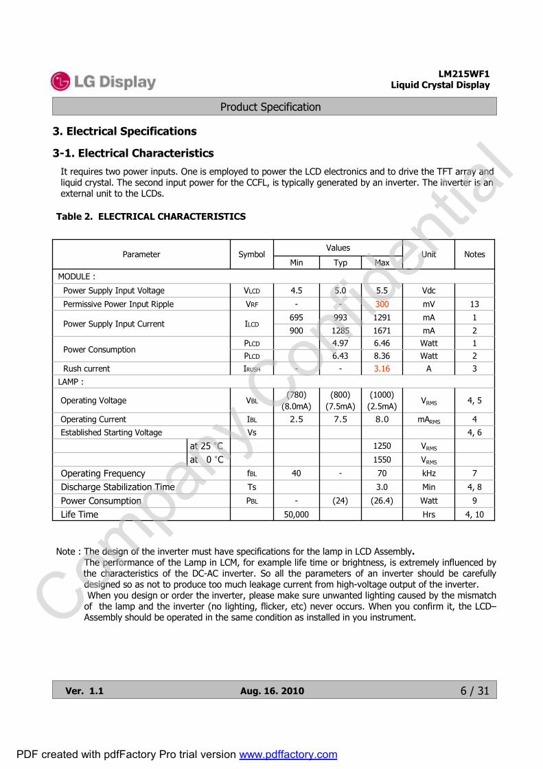
3. Electrical Specifications
3-1. Electrical Characteristics
Table 2. ELECTRICAL CHARACTERISTICS
It requires two power inputs. One is employed to power the LCD electronics and to drive the TFT array and liquid crystal. The second input power for the CCFL, is typically generated by an inverter. The inverter is an external unit to the LCDs.
1Watt6.464.97PLCD
4, 10Hrs50,000Life Time
LAMP :
4, 5VRMS(1000)
(2.5mA)(800)
(7.5mA)(780)
(8.0mA)VBLOperating Voltage
4mARMS8.07.52.5IBLOperating Current
4, 6VsEstablished Starting Voltage
VRMS1250at 25 °CVRMS1550at 0 °C
7kHz70-40fBLOperating Frequency4, 8Min3.0TsDischarge Stabilization Time9Watt(26.4)(24)-PBLPower Consumption
3A3.16--IRUSHRush current
MODULE :
2Watt8.366.43PLCDPower Consumption
Vdc5.55.04.5VLCDPower Supply Input Voltage
13mV300--VRFPermissive Power Input Ripple
1mA1291993695
2mA16711285900ILCDPower Supply Input Current
Parameter SymbolMaxTypMin
NotesUnitValues
Note : The design of the inverter must have specifications for the lamp in LCD Assembly.The performance of the Lamp in LCM, for example life time or brightness, is extremely influenced bythe characteristics of the DC-AC inverter. So all the parameters of an inverter should be carefullydesigned so as not to produce too much leakage current from high-voltage output of the inverter.When you design or order the inverter, please make sure unwanted lighting caused by the mismatch
of the lamp and the inverter (no lighting, flicker, etc) never occurs. When you confirm it, the LCD–Assembly should be operated in the same condition as installed in you instrument.Com
pany
Con
fiden
tial
PDF created with pdfFactory Pro trial version www.pdffactory.com

Product Specification
7 / 31
LM215WF1Liquid Crystal Display
Ver. 1.1 Aug. 16. 2010
Note. Do not attach a conducting tape to lamp connecting wire. If the lamp wire attach to a conducting tape,TFT-LCD Module has a low luminance and the inverter has abnormal action. Because leakage current is occurred between lamp wire and conducting tape.
1. The specified current and power consumption are under the VLCD=5.0V, 25 ± 2°C,fV=60Hz condition whereas mosaic pattern(8 x 6) is displayed and fV is the frame frequency.
2. The current is specified at the full black pattern..3. The duration of rush current is about 5ms and rising time of power Input is 500us ± 20%.(min.).4. Specified values are for a single lamp.5. Operating voltage is measured at 25 ± 2°C, and follows as below condition.
The variance of the voltage is ± 10%. (Based on single Lamp.)The variance of the voltage is ± 20%. (Based on system & Test equipment tolerance.)
6. The voltage above VS should be applied to the lamps for more than 1 second for start-up.(Inverter open voltage must be more than lamp starting voltage.)
Otherwise, the lamps may not be turned on. The used lamp current is the lamp typical current.7. The output of the inverter must have symmetrical(negative and positive) voltage waveform and
symmetrical current waveform (Unsymmetrical ratio is less than 10%). Please do not use the inverter which has unsymmetrical voltage and unsymmetrical current and spike wave. Lamp frequency may produce interface with horizontal synchronous frequency and as a result this maycause beat on the display. Therefore lamp frequency shall be as away possible from the horizontalsynchronous frequency and from its harmonics in order to prevent interference.
8. Let ’s define the brightness of the lamp after being lighted for 5 minutes as 100%.TS is the time required for the brightness of the center of the lamp to be not less than 95%.The used lamp current is the lamp typical current.
9. The lamp power consumption shown above does not include loss of external inverter.The used lamp current is the lamp typical current. (PBL = VBL x IBL x NLamp )
10. The life is determined as the time at which brightness of the lamp is 50% compared to that of initial value at the typical lamp current on condition of continuous operating at 25 ± 2°C.
11. Requirements for a system inverter design, which is intended to have a better display performance, a better power efficiency and a more reliable lamp, are following. It shall help increase the lamp lifetime and reduce leakage current.a. The asymmetry rate of the inverter waveform should be less than 10%.
b. The distortion rate of the waveform should be within √2 ±10%. * Inverter output waveform had better be more similar to ideal sine wave.
I p
I -p
* Asymmetry rate:
| I p – I –p | / Irms x 100%
* Distortion rate
I p (or I –p) / Irms
12. The inverter which is combined with this LCM, is highly recommended to connect coupling(ballast) condenser at the high voltage output side. When you use the inverter which has not coupling(ballast) condenser, it may cause abnormal lamp lighting because of biased mercury as time goes.
13. Permissive power ripple should be measured under VLCD =5.0V, 25°C, fV(frame frequency)=MAXcondition and At that time, we recommend the bandwidth configuration of oscilloscope is to be under20Mhz. See the figure 3.
14. In case of edgy type back light with over 4 parallel lamps, input current and voltage wave form should be synchronized
Compa
ny C
onfid
entia
l
PDF created with pdfFactory Pro trial version www.pdffactory.com

Product Specification
8 / 31
LM215WF1Liquid Crystal Display
Ver. 1.1 Aug. 16. 2010
White pattern Black pattern
• Permissive Power input ripple (VLCD =5.0V, 25°C, fV(frame frequency)=MAX condition)
• Power consumption (VLCD =5.0V, 25°C, fV (frame frequency=60Hz condition)
[ Figure 3 ] Mosaic pattern & Black Pattern for power consumption measurement
Mosaic Pattern
Compa
ny C
onfid
entia
l
PDF created with pdfFactory Pro trial version www.pdffactory.com

Product Specification
9 / 31
LM215WF1Liquid Crystal Display
Ver. 1.1 Aug. 16. 2010
3-2. Interface Connections
Table 3 MODULE CONNECTOR(CN1) PIN CONFIGURATION
-LCD Connector(CN1). :IS100-L30B-C23 (UJU) or Equivalent- Mating Connector : FI-XC30C2L (Manufactured by JAE) or Equivalent
3-2-1. LCD Module
Note: 1. All GND(ground) pins should be connected together and to Vss which should also be connected to the LCD’s metal frame.
2. All VLCD (power input) pins should be connected together.3. Input Level of LVDS signal is based on the IEA 664 Standard.
VLCD
VLCD
VLCD
PWM
NC
NC
GND
SR3P
SR3M
SCLKINP
SCLKINM
SR2P
SR2M
GND
SR1P
Symbol
30
29
28
27
26
25
24
23
22
21
20
19
18
17
16
No
Power +5V
Power +5V
Power +5V
PWM_OUT for control burst frequency of Inverter
NC (reserved I2C communication)
NC (reserved I2C communication)
Ground
+ Signal of even channel 3 (LVDS)
- Signal of even channel 3 (LVDS)
+ Signal of even clock channel (LVDS)
- Signal of even clock channel (LVDS)
+ Signal of even channel 2 (LVDS)
- Signal of even channel 2 (LVDS)
Ground
+ Signal of even channel 1 (LVDS)
Description
- Signal of even channel 1 (LVDS)
Ground
+ Signal of even channel 0 (LVDS)
- Signal of even channel 0 (LVDS)
+ Signal of odd channel 3 (LVDS)
- Signal of odd channel 3 (LVDS)
+ Signal of odd clock channel (LVDS)
- Signal of odd clock channel (LVDS)
Ground
+ Signal of odd channel 2 (LVDS)
- Signal of odd channel 2 (LVDS)
+ Signal of odd channel 1 (LVDS)
- Signal of odd channel 1 (LVDS)
+ Signal of odd channel 0 (LVDS)
- Signal of odd channel 0 (LVDS)
Description
SR1M15
GND14
SR0P13
SR0M12
FR3P11
FR3M10
FCLKINP9
FCLKINM8
GND7
FR2P6
FR2M5
FR1P4
FR1M3
FR0P2
FR0M1
SymbolNo
301
IS100-L30B-C23(UJU)
#1 #30
Rear view of LCM
[ Figure 4 ] User Connector diagramCompa
ny C
onfid
entia
l
PDF created with pdfFactory Pro trial version www.pdffactory.com

Product Specification
10 / 31
LM215WF1Liquid Crystal Display
Ver. 1.1 Aug. 16. 2010
LVDS Input characteristics
NotesUnitMaxMinSymbolDescription
85MHz > Fclk ≥ 65MHzps+ 400- 400tSKEWLVDS Clock to Data Skew Margin
-
65MHz > Fclk ≥ 30MHz
- 1/7
- 600
Tclk+ 1/7tSKEW_EOLVDS Clock to Clock Skew Margin (Even to Odd)
ps+ 600tSKEW
-V2.10.3VINLVDS Input Voltage Range
-V1.80.6VCMLVDS Common mode Voltage
-mV600200|VID|LVDS Differential Voltage
NotesUnitMaxMinSymbolDescription
1. DC Specification
2. AC Specification
LVDS Even Data
LVDS Odd Clock
LVDS Even Clock
t SKEW_ EO
T clk
T clk
LVDS Data
t SKEW
LVDS Clock
Tclk
t SKEW ( Fclk = 1 / Tclk )t SKEW ( Fclk = 1 / Tclk )1 ) 85MHz > Fclk ≥65MHz : -400 ~ + 4002 ) 65MHz > Fclk ≥30MHz : -600 ~ + 600
Compa
ny C
onfid
entia
l
PDF created with pdfFactory Pro trial version www.pdffactory.com

Product Specification
11 / 31
LM215WF1Liquid Crystal Display
Ver. 1.1 Aug. 16. 2010
< Clock skew margin between channel >
< LVDS Data Format >
3. Data Format1) LVDS 2 Port
Compa
ny C
onfid
entia
l
PDF created with pdfFactory Pro trial version www.pdffactory.com

Product Specification
12 / 31
LM215WF1Liquid Crystal Display
Ver. 1.1 Aug. 16. 2010
Table 4. BACKLIGHT CONNECTOR PIN CONFIGURATION(CN2,CN3,CN4,CN5)
The backlight interface connector is a model 35001HS-02LD manufactured by Yeonho. The mating connector part number are 35001WR-02L or equivalent. The pin configuration for the connector is shown in the table below.
1, 2
1
NOTES
Low Voltage for Lamp
High Voltage for Lamp
Description
LV
HV
Symbol
2
1
Pin
[ Figure 5 ] Backlight connector diagram
Note : 1. The high voltage power terminal is colored pink, whiteThe low voltage pin color is sky blue, white.
2. The backlight ground should be common with LCD metal frame.3. 35001HS-02LD (Locking type)
Up Side
Down Side
CN2
CN3
CN4
CN5
Lamp1
Lamp2
Lamp3
Lamp4
Compa
ny C
onfid
entia
l
PDF created with pdfFactory Pro trial version www.pdffactory.com
Product Specification
13 / 31
LM215WF1Liquid Crystal Display
Ver. 1.1 Aug. 16. 2010
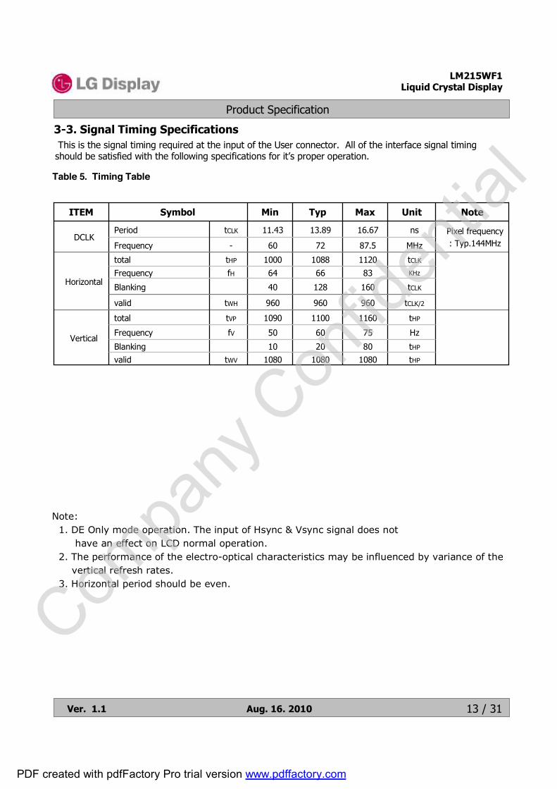
3-3. Signal Timing SpecificationsThis is the signal timing required at the input of the User connector. All of the interface signal timing should be satisfied with the following specifications for it’s proper operation.
Table 5. Timing Table
tHP802010Blanking
tCLK16012840Blanking
tHP108010801080tWVvalid
Hz756050fVFrequency
tHP116011001090tVPtotal
Vertical
tCLK/2960960960tWHvalid
KHz836664fHFrequencytCLK112010881000tHPtotal
Horizontal
MHz87.57260-Frequency
Pixel frequency: Typ.144MHz
ns16.6713.8911.43tCLKPeriodDCLK
NoteUnitMaxTypMinSymbolITEM
Note:1. DE Only mode operation. The input of Hsync & Vsync signal does not
have an effect on LCD normal operation.2. The performance of the electro-optical characteristics may be influenced by variance of the
vertical refresh rates.3. Horizontal period should be even.
Compa
ny C
onfid
entia
l
PDF created with pdfFactory Pro trial version www.pdffactory.com

Product Specification
14 / 31
LM215WF1Liquid Crystal Display
Ver. 1.1 Aug. 16. 2010
3-4. Signal Timing Waveforms
Dclk
tCLK
Valid
InvalidInvalid
DE(Data Enable)
DatatSI tHI
tSD tHD
DE(Data Enable)
tVV
tVP
DE
DE(Data Enable)
tHP
tHV
DE
1. DCLK , DE, DATA waveforms
2. Horizontal waveform
3. Vertical waveform
tHP
Compa
ny C
onfid
entia
l
PDF created with pdfFactory Pro trial version www.pdffactory.com

Product Specification
15 / 31
LM215WF1Liquid Crystal Display
Ver. 1.1 Aug. 16. 2010
3-5. Color Input Data Reference
Table 6. COLOR DATA REFERENCE
The Brightness of each primary color(red,green,blue) is based on the 8-bit gray scale data input for the color;the higher the binary input, the brighter the color. The table below provides a reference for color versus data input.
0 0 0 0 0 0 0 00 0 0 0 0 0 0 00 0 0 0 0 0 0 0GREEN (000) Dark
GREEN
0 0 0 0 0 0 0 00 0 0 0 0 0 0 10 0 0 0 0 0 0 0GREEN (001)
............
0 0 0 0 0 0 0 01 1 1 1 1 1 1 00 0 0 0 0 0 0 0GREEN (254)
0 0 0 0 0 0 0 01 1 1 1 1 1 1 10 0 0 0 0 0 0 0GREEN (255)
0 0 0 0 0 0 0 00 0 0 0 0 0 0 00 0 0 0 0 0 0 0RED (000) Dark
RED
0 0 0 0 0 0 0 00 0 0 0 0 0 0 00 0 0 0 0 0 0 1RED (001)
............
0 0 0 0 0 0 0 00 0 0 0 0 0 0 01 1 1 1 1 1 1 0RED (254)
0 0 0 0 0 0 0 00 0 0 0 0 0 0 01 1 1 1 1 1 1 1RED (255)
0 0 0 0 0 0 0 10 0 0 0 0 0 0 00 0 0 0 0 0 0 0BLUE (001)
............
1 1 1 1 1 1 1 00 0 0 0 0 0 0 00 0 0 0 0 0 0 0BLUE (254)
1 1 1 1 1 1 1 10 0 0 0 0 0 0 00 0 0 0 0 0 0 0BLUE (255)
BLUE (000) Dark
White
Yellow
Magenta
Cyan
Blue (255)
Green (255)
Red (255)
Black 0 0 0 0 0 0 0 00 0 0 0 0 0 0 00 0 0 0 0 0 0 0
BasicColor
0 0 0 0 0 0 0 00 0 0 0 0 0 0 01 1 1 1 1 1 1 1
0 0 0 0 0 0 0 01 1 1 1 1 1 1 10 0 0 0 0 0 0 0
1 1 1 1 1 1 1 10 0 0 0 0 0 0 00 0 0 0 0 0 0 0
1 1 1 1 1 1 1 11 1 1 1 1 1 1 10 0 0 0 0 0 0 0
1 1 1 1 1 1 1 10 0 0 0 0 0 0 01 1 1 1 1 1 1 1
0 0 0 0 0 0 0 01 1 1 1 1 1 1 11 1 1 1 1 1 1 1
1 1 1 1 1 1 1 11 1 1 1 1 1 1 11 1 1 1 1 1 1 1
BLUEMSB LSB
GREENMSB LSB
REDMSB LSB
B7 B6 B5 B4 B3 B2 B1 B0G7 G6 G5 G4 G3 G2 G1 G0R7 R6 R5 R4 R3 R2 R1 R0
0 0 0 0 0 0 0 00 0 0 0 0 0 0 00 0 0 0 0 0 0 0
BLUE
Color
Input Color Data
Compa
ny C
onfid
entia
l
PDF created with pdfFactory Pro trial version www.pdffactory.com

Product Specification
16 / 31
LM215WF1Liquid Crystal Display
Ver. 1.1 Aug. 16. 2010
3-6. Power Sequence
Notes : 1. Please avoid floating state of interface signal at invalid period.2. When the interface signal is invalid, be sure to pull down the power supply for LCD VLCDto 0V.3. Lamp power must be turn on after power supply for LCD and interface signal are valid.
ms---T6
s-1T7
ms50-0.01T2
ms
ms--500T3
--200T4
ms50-0.01T5
ms10-0.5T1
MaxTypMinUnits
ValuesParameter
Table 7. POWER SEQUENCE
Interface Signal, Vi(Digital RGB signal, SCDT ,Vsync, Hsync, DE, Clock to PanelLink Transmitter)
Power Supply for Backlight Inverter
Power Supply, VLCD
90%VLCD 90%
10% 10%
T10V
LAMP ONLAMP OFF
T3
0V
T6
LAMP OFF
T4
T2 T5 T7
Valid Data
[ Figure 6 ] Power sequence
Compa
ny C
onfid
entia
l
PDF created with pdfFactory Pro trial version www.pdffactory.com

Product Specification
17 / 31
LM215WF1Liquid Crystal Display
Ver. 1.1 Aug. 16. 2010
3-7. VLCD Power Dip Condition
1) Dip condition
3.5V ≤VLCD< 4.5V , td≤20ms
2) VLCD< 3.5V
VLCD-dip conditions should also follow the Power On/Off conditions for supply voltage.
4.5V
3.5V
VLCD
td
[ Figure 7 ] Power dip condition
Compa
ny C
onfid
entia
l
PDF created with pdfFactory Pro trial version www.pdffactory.com

Product Specification
18 / 31
LM215WF1Liquid Crystal Display
Ver. 1.1 Aug. 16. 2010
Optical characteristics are determined after the unit has been ‘ON’ for approximately 30 minutesin a dark environment at 25±2°C. The values specified are at an approximate distance 50cm from the LCDsurface at a viewing angle of Φ and θ equal to 0 ° and aperture 1 degree.FIG. 8 presents additional information concerning the measurement equipment and method.
Table 8. OPTICAL CHARACTERISTICS (Ta=25 °C, VLCD=5.0V, fV=60Hz Dclk=144MHz, IBL=7.5mA)
4. Optical Specifications
VerticalHorizontal
-170140θV 6(PR-880)
Degree-176150θHCR>5
Viewing Angle (CR>5)
Fig 11(PR880)
1.73LRLuminance uniformity-Angular dependence(TCO’5.0)
5(PR-650)
72%Color Gamut
ms5Ttotal
1(PR-880)
1000700CRContrast Ratio
7(PR880)
2.2Gray Scale
VerticalHorizontal
-160130θVDegree
-170140θHGeneral (CR>10)
Viewing Angle (CR>10)
WHITE
BLUE
GREEN
RED
0.616Gy
0.303Gx
0.067By0.147Bx
0.329Wy
0.313Wx
Decay TimeRise Time
ms7.43.7-TrD
0.334Ry
(PR-650)Typ
+0.03
0.646
Typ-0.03
Rx
Color Coordinates [CIE1931]
4(RD80S)
ms2.61.3-TrR
Response Time
3(PR-880)
%75δ WHITELuminance Variation
2(PR-880)
cd/m2300250LWHSurface Luminance, white
NotesUnitsMaxTypMin
ValuesSymbolParameter
[ Figure 8 ] Optical characteristic measurement equipment and method50cm
Optical Stage(x,y) LCD ModulePritchard 880 or
equivalent
Compa
ny C
onfid
entia
l
PDF created with pdfFactory Pro trial version www.pdffactory.com

Product Specification
19 / 31
LM215WF1Liquid Crystal Display
Ver. 1.1 Aug. 16. 2010
pixels black all with Luminance Surfacepixels white all with Luminance Surface
RatioContrast =
100)L .... ,L ,(L Maximum)L .. ,L,Minimum(L
P9P2P1
P9P2P1 ×…
=WHITEδ
Notes 1. Contrast Ratio(CR) is defined mathematically as :
It is measured at center point(Location P1)
2. Surface luminance is the luminance value at center 1 point(1) acrossthe LCD surface 50cm from the surface with all pixels displaying white. For more information see FIG 9.
3. The variation in surface luminance , δ WHITE is defined as :
For more information see FIG 9.
4. Response time is the time required for the display to transition from black to white (Rise Time, TrR) and from white to black (Decay Time, TrD). For additional information see FIG 10.
5. Color gamut is calculated from CIE 1931 space.
6. Viewing angle is the angle at which the contrast ratio is greater than 5 or 10. The angles aredetermined for the horizontal or x axis and the vertical or y axis with respect to the z axis whichis normal to the LCD surface. For more information see FIG 12.
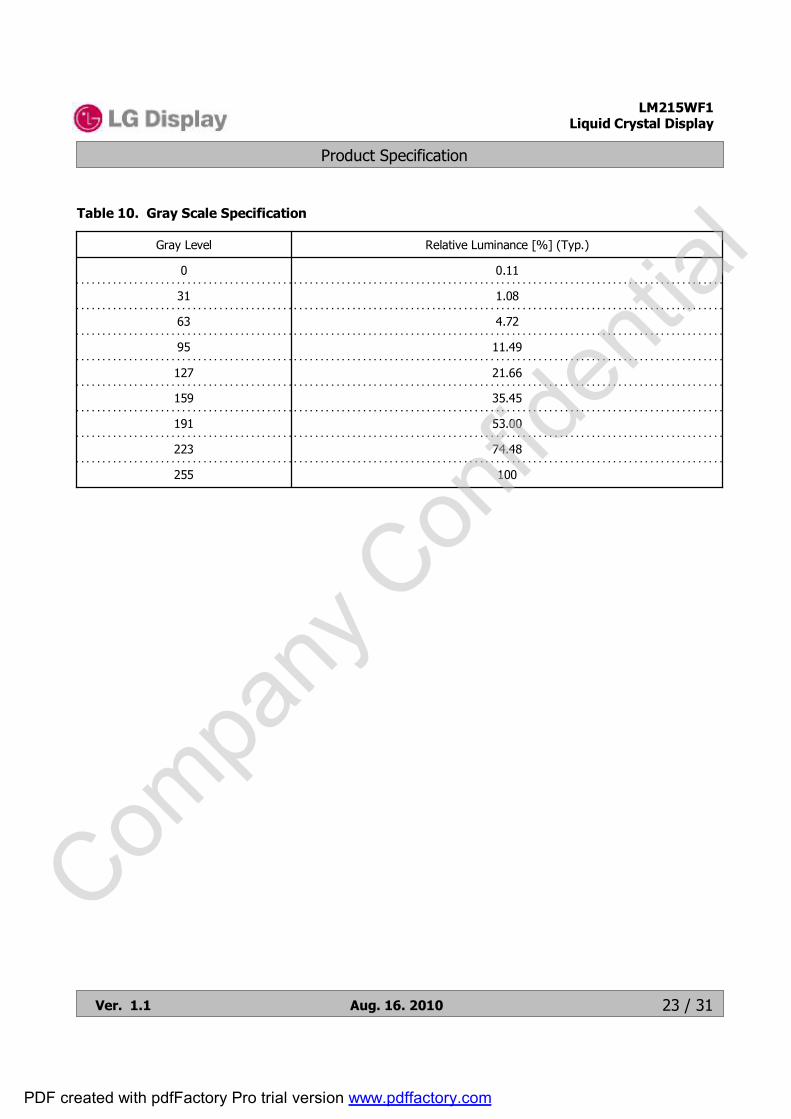
7. Gray scale specificationGamma Value is approximately 2.2. For more information see Table 10.
Compa
ny C
onfid
entia
l
PDF created with pdfFactory Pro trial version www.pdffactory.com

Product Specification
20 / 31
LM215WF1Liquid Crystal Display
Ver. 1.1 Aug. 16. 2010
The response time is defined as the following figure and shall be measured by switching the input signal for “black” and “white”.
[ FIG 10 ] Response Time
Measuring point for surface luminance & measuring point for luminance variation.
[ FIG 9 ] Measure Point for Luminance
<Measuring point for luminance variation> <Measuring point for surface luminance>H
H/2
V/2
V
@ H,V : Active AreaActive Area
1
42
7
H
V
3
5 6
8 9V/10
V/2
H/2 H/10
10090
100
[%]
Optical
responsewhite black white
TrR TrD
Compa
ny C
onfid
entia
l
PDF created with pdfFactory Pro trial version www.pdffactory.com

Product Specification
21 / 31
LM215WF1Liquid Crystal Display
Ver. 1.1 Aug. 16. 2010
Notes :
Luminance Uniformity - angular – dependence (LR& TB)
H
CL RV/2
V/2
H/10 H/10
T
B
V/10
V/10
V
D
< Luminance uniformity - angular dependence measuring point >
FIG. 11 Luminance Uniformity angular dependence
TCO 5.0 Luminance uniformity – angular dependence, is the capacity of the FPD to maintain a certain luminance level independently of the viewing direction, The angular-dependent luminance uniformity is defined as the ratio of maximum luminance to minimum luminance in the specified measurement areas.
- Test pattern : Full white 4˚× 4˚square size, back ground shall be set to 80%image loading, RGB 204, 204, 204
- Test luminance : ≥150cd/㎡- Test point : 5-point- Test distance : D * 1.5 = 82㎝- Test method : LR = ((Lmax.+30deg. / Lmin. +30deg.) + (Lmax. -30deg. / Lmin. -30deg.)) / 2
TB = ((Lmax.+15deg. / Lmin. +15deg.)
Compa
ny C
onfid
entia
l
PDF created with pdfFactory Pro trial version www.pdffactory.com

Product Specification
22 / 31
LM215WF1Liquid Crystal Display
Ver. 1.1 Aug. 16. 2010
[ FIG 12 ] Viewing angle
Dimension of viewing angle range.
Normal Y E
φ
θ
φ = 0°, Right
φ = 180°, Left
φ = 270°, Down
φ = 90°, Up
br LaVL += )log()log()log( aVrLL b +=−
Here the Parameter α and γ relate the signal level V to the luminance L.The GAMMA we calculate from the log-log representation (FIG. 14)
[ FIG 13 ] Sample Luminance vs. gray scale (using a 256 bit gray scale)
[ FIG 14 ] Sample Log-log plot of luminance vs. gray scale
Compa
ny C
onfid
entia
l
PDF created with pdfFactory Pro trial version www.pdffactory.com
Product Specification
23 / 31
LM215WF1Liquid Crystal Display
Ver. 1.1 Aug. 16. 2010
Table 10. Gray Scale Specification
0.110
100
74.48
53.00
35.45
21.66
11.49
4.72
1.08
255
223
191
159
127
95
63
31
Relative Luminance [%] (Typ.)Gray Level
Compa
ny C
onfid
entia
l
PDF created with pdfFactory Pro trial version www.pdffactory.com

Product Specification
24 / 31
LM215WF1Liquid Crystal Display
Ver. 1.1 Aug. 16. 2010
5. Mechanical Characteristics
The contents provide general mechanical characteristics. In addition the figures in the next page are detailed mechanical drawing of the LCD.
268.11mmVertical
Hard coating(3H)Anti-Glare treatment of the front polarizerSurface Treatment
2100g(typ)Weight
271.31mmVertical
292.2mm ± 0.5mmVertical
16.5mm ± 0.5mmDepth
476.64mmHorizontalActive Display Area
479.84mmHorizontalBezel Area
495.6mm ± 0.5mmHorizontal
Outline Dimension
Notes : Please refer to a mechanic drawing in terms of tolerance at the next page.
Compa
ny C
onfid
entia
l
PDF created with pdfFactory Pro trial version www.pdffactory.com

Product Specification
25 / 31
LM215WF1Liquid Crystal Display
Ver. 1.1 Aug. 16. 2010
<FRONT VIEW>
Compa
ny C
onfid
entia
l
PDF created with pdfFactory Pro trial version www.pdffactory.com

Product Specification
26 / 31
LM215WF1Liquid Crystal Display
Ver. 1.1 Aug. 16. 2010
<REAR VIEW>
Compa
ny C
onfid
entia
l
PDF created with pdfFactory Pro trial version www.pdffactory.com

Product Specification
27 / 31
LM215WF1Liquid Crystal Display
Ver. 1.1 Aug. 16. 2010
6. Reliability
Environment test condition
Ta= 40 °C ,90%RHHumidity condition Operation7
0 - 40,000 feet(12192m)Altitude
storage / shipment8
Shock level : 100GWaveform : half sine wave, 2msDirection :±X, ±Y, ±Z
One time each direction
Shock test(non-operating)6
Wave form : randomVibration level : 1.0G RMSBandwidth : 10-300HzDuration : X,Y,Z, 10 min
One time each direction
Vibration test(non-operating)5
Ta= 0°C 240hLow temperature operation test4
Ta= 50°C 50%RH 240hHigh temperature operation test3
Ta= -20°C 240hLow temperature storage test2
Ta= 60°C 240hHigh temperature storage test1
ConditionTest ItemNo
Compa
ny C
onfid
entia
l
PDF created with pdfFactory Pro trial version www.pdffactory.com

Product Specification
28 / 31
LM215WF1Liquid Crystal Display
Ver. 1.1 Aug. 16. 2010
7. International standards
7-1. Safety
7-2. EMC
a) ANSI C63.4 “Methods of Measurement of Radio-Noise Emissions from Low-Voltage Electrical and Electrical Equipment in the Range of 9kHZ to 40GHz. “American National Standards Institute(ANSI),1992
b) C.I.S.P.R “Limits and Methods of Measurement of Radio Interface Characteristics of Information Technology Equipment.“ International Special Committee on Radio Interference.
c) EN 55022 “Limits and Methods of Measurement of Radio Interface Characteristics of Information Technology Equipment.“ European Committee for Electro-technical Standardization.(CENELEC), 1998 ( Including A1: 2000 )
a) UL 60950-1:2003, First Edition, Underwriters Laboratories, Inc.,Standard for Safety of Information Technology Equipment.
b) CAN/CSA C22.2, No. 60950-1-03 1st Ed. April 1, 2003, Canadian Standards Association,Standard for Safety of Information Technology Equipment.
c) EN 60950-1:2001, First Edition, European Committee for Electro-technical Standardization(CENELEC)European Standard for Safety of Information Technology Equipment.
d) RoHS, Directive 2002/95/EC of the European Parliament and of the council of 27January 2003
7-3. Environment
a) RoHS, Directive 2002/95/EC of the European Parliament and of the council of 27January 2003
Compa
ny C
onfid
entia
l
PDF created with pdfFactory Pro trial version www.pdffactory.com

Product Specification
29 / 31
LM215WF1Liquid Crystal Display
Ver. 1.1 Aug. 16. 2010
8. Packing
8-1. Designation of Lot Mark
a) Lot Mark
A B C D E F G H I J K L M
A,B,C : SIZE(INCH) D : YEAR E : MONTH F ~ M : SERIAL NO.
Note1. YEAR
2. MONTH
Mark
Year
0
2010
6
2006
7
2007
8
2008
9
2009
4
2004
5
2005
321
200320022001
B
Nov
Mark
Month
A
Oct
6
Jun
7
Jul
8
Aug
9
Sep
4
Apr
5
May
C321
DecMarFebJan
b) Location of Lot Mark
Serial No. is printed on the label. The label is attached to the backside of the LCD module.This is subject to change without prior notice.
a) Package quantity in one box : 7pcs
b) Box Size : 370mm x 320mm x 580mm
8-2. Packing Form
Compa
ny C
onfid
entia
l
PDF created with pdfFactory Pro trial version www.pdffactory.com

Product Specification
30 / 31
LM215WF1Liquid Crystal Display
Ver. 1.1 Aug. 16. 2010
9. PRECAUTIONS
Please pay attention to the followings when you use this TFT LCD module.
9-1. MOUNTING PRECAUTIONS
(1) You must mount a module using holes arranged in four corners or four sides.(2) You should consider the mounting structure so that uneven force (ex. Twisted stress) is not applied to the
module. And the case on which a module is mounted should have sufficient strength so that external force is not transmitted directly to the module.
(3) Please attach the surface transparent protective plate to the surface in order to protect the polarizer.Transparent protective plate should have sufficient strength in order to the resist external force.
(4) You should adopt radiation structure to satisfy the temperature specification.(5) Acetic acid type and chlorine type materials for the cover case are not desirable because the former
generates corrosive gas of attacking the polarizer at high temperature and the latter causes circuit break by electro-chemical reaction.
(6) Do not touch, push or rub the exposed polarizers with glass, tweezers or anything harder than HBpencil lead. And please do not rub with dust clothes with chemical treatment.Do not touch the surface of polarizer for bare hand or greasy cloth.(Some cosmetics are detrimentalto the polarizer.)
(7) When the surface becomes dusty, please wipe gently with absorbent cotton or other soft materials like chamois soaks with petroleum benzene. Normal-hexane is recommended for cleaning the adhesives used to attach front / rear polarizers. Do not use acetone, toluene and alcohol because they cause chemical damage to the polarizer.
(8) Wipe off saliva or water drops as soon as possible. Their long time contact with polarizer causes deformations and color fading.
(9) Do not open the case because inside circuits do not have sufficient strength.
9-2. OPERATING PRECAUTIONS
(1) The spike noise causes the mis-operation of circuits. It should be lower than following voltage : V=±200mV(Over and under shoot voltage)
(2) Response time depends on the temperature.(In lower temperature, it becomes longer.)(3) Brightness depends on the temperature. (In lower temperature, it becomes lower.)
And in lower temperature, response time(required time that brightness is stable after turned on) becomeslonger.
(4) Be careful for condensation at sudden temperature change. Condensation makes damage to polarizer or electrical contacted parts. And after fading condensation, smear or spot will occur.
(5) When fixed patterns are displayed for a long time, remnant image is likely to occur.(6) Module has high frequency circuits. Sufficient suppression to the electromagnetic interference shall be
done by system manufacturers. Grounding and shielding methods may be important to minimized theinterference.
(7) Please do not give any mechanical and/or acoustical impact to LCM. Otherwise, LCM can’t be operated its full characteristics perfectly.
(8) A screw which is fastened up the steels should be a machine screw. (if not, it causes metallic foreign material and deal LCM a fatal blow)
(9) Please do not set LCD on its edge.
Compa
ny C
onfid
entia
l
PDF created with pdfFactory Pro trial version www.pdffactory.com

Product Specification
31 / 31
LM215WF1Liquid Crystal Display
Ver. 1.1 Aug. 16. 2010
Since a module is composed of electronic circuits, it is not strong to electrostatic discharge. Make certain that treatment persons are connected to ground through wrist band etc. And don’t touch interface pin directly.
9-3. ELECTROSTATIC DISCHARGE CONTROL
Strong light exposure causes degradation of polarizer and color filter.
9-4. PRECAUTIONS FOR STRONG LIGHT EXPOSURE
When storing modules as spares for a long time, the following precautions are necessary.
(1) Store them in a dark place. Do not expose the module to sunlight or fluorescent light. Keep the temperature between 5°C and 35°C at normal humidity.
(2) The polarizer surface should not come in contact with any other object.It is recommended that they be stored in the container in which they were shipped.
9-5. STORAGE
9-6. HANDLING PRECAUTIONS FOR PROTECTION FILM
(1) The protection film is attached to the bezel with a small masking tape.When the protection film is peeled off, static electricity is generated between the film and polarizer.This should be peeled off slowly and carefully by people who are electrically grounded and with well ion-blown equipment or in such a condition, etc.
(2) When the module with protection film attached is stored for a long time, sometimes there remains a very small amount of glue still on the bezel after the protection film is peeled off.
(3) You can remove the glue easily. When the glue remains on the bezel surface or its vestige is recognized, please wipe them off with absorbent cotton waste or other soft material like chamois soaked with normal-hexane.
Compa
ny C
onfid
entia
l
PDF created with pdfFactory Pro trial version www.pdffactory.com