Embed Size (px)
Citation preview
Product Specification
1 /31
LC420WU5
Ver. 0.0
42.0¡ WUXGA TFT LCDTitle
MODEL
GeneralBUYER
*When you obtain standard approval,please use the above model name without suffix
LC420WU5*MODEL
SLA2SUFFIX
LG.Philips LCD Co., Ltd.SUPPLIER
FORAPPROVAL
SPECIFICATION
TV Product Development Dept.LG. Philips LCD Co., Ltd
PREPARED BY
REVIEWED BY
SIGNATUREDATEAPPROVED BY
Please return 1 copy for your confirmation with
your signature and comments.
/
/
/
SIGNATURE DATEAPPROVED BY
))
((
Final SpecificationPreliminary Specification

Product Specification
2 /31
LC420WU5
Ver. 0.0
CONTENTS
26HANDLING PRECAUTIONS FOR PROTECTION FILM9-6
27~31Appendix
10SIGNAL TIMING SPECIFICATIONS3-3
25PRECAUTIONS9
25MOUNTING PRECAUTIONS9-1
25OPERATING PRECAUTIONS9-2
26ELECTROSTATIC DISCHARGE CONTROL9-3
26PRECAUTIONS FOR STRONG LIGHT EXPOSURE9-4
26STORAGE9-5
12
8INTERFACE CONNECTIONS3-2
COLOR DATA REFERENCE3-5
24DESIGNATION OF LOT MARK8-1
24PACKING FORM8-2
24PACKING8
23EMC7-2
1COVER
2CONTENTS
3RECORD OF REVISIONS
4GENERAL DESCRIPTION1
5ABSOLUTE MAXIMUM RATINGS2
6ELECTRICAL SPECIFICATIONS3
6ELECTRICAL CHARACTERISTICS3-1
11SIGNAL TIMING WAVEFORMS3-4
13POWER SEQUENCE3-6
15OPTICAL SPECIFICATIONS4
19MECHANICAL CHARACTERISTICS5
22RELIABILITY6
23INTERNATIONAL STANDARDS7
23SAFETY7-1
PageITEMNumber

Product Specification
3 /31
LC420WU5
Ver. 0.0
Preliminary Specification(First Draft) -Apr, 19, 20070.0
Update Current and Power Consumption (Not Fixed) 4, 6June, 25, 20070.1
Update Notes 5.9
Update Table 11(Color Coordinates_ Not Fixed)15
Update Pallet Ass¡y29
Update Pallet Label31
Update Table 3(Not Fixed)7
DescriptionPageRevision DateRevision No.
RECORD OF REVISIONS
Product Specification
4 /31
LC420WU5
Ver. 0.0
General Features
1. General Description
CN1(51pin)
LVDS2Port
Source Driver Circuit
TFT - LCD Panel(1920 ¡ RGB ¡ 1080 pixels)
G1
S1 S1920
G1080
Mini-LVDS(RGB)
Timing Controller[LVDS Rx + DCR + ODC
integrated]
Gate D
river Circuit
EEPROM
Power Circuit Block
SDASCL+12.0V
SDRAM
MEMCTRL RGB
DCREnable
VBR_OUT
Back light Assembly3PinX1CN(High)
3PinX1CN(High)
+24.0V, GND, VBR-A, VBR-BStatus Inverter(Master)
Inverter(Slave)+24.0V, GND
Viewing angle free ( R/L 178 (Typ.), U/D 178 (Typ.))Viewing Angle (CR>10)
8-bit, 16.7 M colorsColor Depth
1920 horiz. by 1080 vert. Pixels, RGB stripe arrangementPixel Format
500 cd/m2 (Center 1point ,Typ.)Luminance, White
Total 168.8 W (Typ.) (Logic = (8.8) W, Inverter = (160) W [VBR-A=1.65V] ) Power Consumption
(11.5Kg) (Typ.) Weight
Transmissive mode, Normally blackDisplay Mode
Hard coating(3H), Anti-glare treatment of the front polarizer (Haze 13%)Surface Treatment
0.4845 mm x 0.4845 mmPixel Pitch
983.0(H) x 576.0 (V) x 51.0 mm(D) (Typ.)Outline Dimension
42.02 inches(1067.31mm) diagonalActive Screen Size
The LC420WU5 is a Color Active Matrix Liquid Crystal Display with an integral External Electrode FluorescentLamp(EEFL) backlight system. The matrix employs a-Si Thin Film Transistor as the active element.It is a transmissive display type which is operating in the normally black mode. It has a 42.02 inch diagonally measured active display area with WUXGA resolution (1080 vertical by 1920 horizontal pixel array).Each pixel is divided into Red, Green and Blue sub-pixels or dots which are arrayed in vertical stripes.Gray scale or the luminance of the sub-pixel color is determined with a 8-bit gray scale signal for each dot.Therefore, it can present a palette of more than 16.7M(true) colors. It has been designed to apply the 8-bit 2-port LVDS interface.It is intended to support LCD TV, PCTV where high brightness, super wide viewing angle, high color gamut,high color depth and fast response time are important.
Product Specification
5 /31
LC420WU5
Ver. 0.0
Notes : 1. Temperature and relative humidity range are shown in the figure below. Wet bulb temperature should be 39 ¡C Max, and no condensation.
2. Gravity mura can be guaranteed under 40condition.
The following items are maximum values which, if exceeded, may cause faulty operation or damage to theLCD module.
Table 1. ABSOLUTE MAXIMUM RATINGS
2. Absolute Maximum Ratings
VDC+5.00VBRBrightness Control Voltage
Note 1,2
¡C+500TOPOperating Temperature
VDC+27.0+21.6VBLBacklight inverter
LCM
Unit
%RH9010HOPOperating Ambient Humidity
%RH9010HSTStorage Humidity
¡C+60-20TSTStorage Temperature
VDC+5. 5-0.3VON/OFFON/OFF Control Voltage
at 25 ± 2 ¡CVDC+14.0+8.0VLCDPower InputVoltage
MaxMinParameter Remark
ValueSymbol
90%
10 20 30 40 50 60 70 800-20
010
20
30
40
50
Dry Bulb Temperature [¡C]
Wet BulbTemperature [¡C]
Storage
Operation
Hum
idity
[(%
)RH
]
10%
40%
60%
60

Product Specification
6 /31
LC420WU5
Ver. 0.0
It requires two power inputs. One is employed to power for the LCD circuit. The other Is used for the EEFL backlight and inverter circuit.
Table 2. ELECTRICAL CHARACTERISTICS
Notes : 1. The specified current and power consumption are under the VLCD=12.0V, 25 ± 2¡C, fV=60Hz condition whereas mosaic pattern(8 x 6) is displayed and fV is the frame frequency.
2. The current is specified at the maximum current pattern.3. The duration of rush current is about 2ms and rising time of power input is 1ms (min)
Mosaic Pattern(8 x 6)
White : 255GrayBlack : 0Gray
3. Electrical Specifications3-1. Electrical Characteristics
1mA( 845)( 734)-
1Watt( 10 . 14)( 8 . 8)-PLCDPower Consumption
3A(3)--IRUSHRush current
VDC12.612.011.4VLCDPower Input Voltage
2mA( 996)( 866)-ILCDPower Input Current
Circuit :
Parameter SymbolMaxTypMin
NoteUnitValue

Product Specification
7 /31
LC420WU5
Ver. 0.0
Table 3. ELECTRICAL CHARACTERISTICS (Continue)
Power Consumption
IBL_BBefore Aging
IBL_AAfter AgingPower SupplyInput Current
5Hrs50,000Life Time4min3TsDischarge Stabilization Time
Brightness Adjust
VBR-A = 3.3V ¡ 2A(8.5 )8-
VBR-A = 3.3V ¡ 1A(8 )7.5-
VBR-A = 1.65V ¡ 1W(172 )160 -PBL
VBR-A = 1.65V ¡ 1A(7.2 )6.7-1Vp-p0.5--Power Supply Input Voltage Ripple
VBR-A = 1.65V ¡ 2A(7.7 )7.2-
1
VBL = 22.8VVBR-B = 3.3VVBR-A = 1.65V
A(9.6)--IrushPower Supply Input Current (In-Rush)
3V3.3-0VBR-B
Lamp:
Inverter :
Vdc3.31.650.0VBR-ABrightness AdjustInput Voltage for Control System
Signals
Vdc25.224.022.8VBLPower Supply Input Voltage
On/OffOffOn Vdc5.0-2.5V on
Vdc0.80.0-0.3V off
Parameter SymbolMaxTypMin
NotesUnitValues
Notes :1. Electrical characteristics are determined after the unit has been ¡ON¡ and stable for approximately 120
minutes at 25¡ 2¡C. The specified current and power consumption are under the typical supply Input voltage24Vand VBR (VBR-A : 1.65V & VBR-B :3.3V), it is total power consumption.
The ripple voltage of the power supply input voltage is under 0.5 Vp-p. LPL recommend Input Voltage is24.0V ¡ 5%.
2. Electrical characteristics are determined within 30 minutes at 25¡ 2¡C. The specified currents are under the typical supply Input voltage 24V.
3. Brightness Control.This VBR-B Voltage control brightness.
Maximum Duty (100%)3.3VMinimum Duty (20%)0VFunctionVBR-B VoltageFunctionVBR-B Voltage
. 4. The brightness of the lamp after lighted for 5minutes is defined as 100%.
TS is the time required for the brightness of the center of the lamp to be not less than 95% at typical current.The screen of LCD module may be partially dark by the time the brightness of lamp is stable after turn on.
5. Specified Values are for a single lamp which is aligned horizontally. The life time is determined as the time which luminance of the lamp is 50% compared to that of initial value at the typical lamp current (VBR-A : 1.65V & VBR-B :3.3V), on condition of continuous operating at 25 ± 2¡C
Product Specification
8 /31
LC420WU5
Ver. 0.0
Table 4. MODULE CONNECTOR(CN1) PIN CONFIGURATION
- LCD Connector(CN1): FI-R51S-HF(manufactured by JAE) or KN25-51P-0.5SH(manufactured by Hirose)- Mating Connector : FI-R51HL(JAE) or compatible
This LCD module employs two kinds of interface connection, a 51-pin connector is used for the module electronics and Master 14-pin and Slave 12-pin connectors are used for the integral backlight system.
3-2-1. LCD Module
3-2. Interface Connections
Notes :1. The pin no 44 is LCD Test option. ¡AGP¡ (Auto Generation LCM operates Pattern) or ¡NSB¡ (No Signal
Black) is case that LVDS signals are out of frequency or abnormal condition in spite of 12 volt power supply. LPL recommends ¡NSB¡. ( AGP : ¡VCC¡ or ¡OPEN¡ / NSB : ¡GND¡ )
2. All GND(ground) pins should be connected together to the LCD module¡s metal frame. 3. All VLCD (power input) pins should be connected together. 4. All Input levels of LVDS signals are based on the IEA 664 Standard.5. Specific pins(pin No. #1~#10) are used for internal data process of the LCD module.
If not used, these pins are no connection. 6. If DCR function should be enable(¡H¡), 10th pin must be connected to serial resistor which value is under
1k ohm.
-515049484746454443424140393837363534333231
302928
27
No
-
Power Supply +12.0VPower Supply +12.0VPower Supply +12.0VPower Supply +12.0VNo connectionGroundGroundGroundNo connection or GNDNo connection or GNDNo ConnectionNo ConnectionSECOND CHANNEL 3+SECOND CHANNEL 3-
GroundSECOND CLOCK CHANNEL C+SECOND CLOCK CHANNEL C-
GroundSECOND CHANNEL 2+SECOND CHANNEL 2-SECOND CHANNEL 1+
SECOND CHANNEL 1-SECOND CHANNEL 0+SECOND CHANNEL 0-
No connection or GND
Description
-
VLCDVLCDVLCDVLCD
NCGNDGNDGND
Reserved Reserved Reserved (NC)Reserved (NC)
RE3PRE3NGND
RECLKPRECLKN
GNDRE2PRE2NRE1P
RE1NRE0PRE0N
Reserved
Symbol
No ConnectionReserved (NC)25
No ConnectionReserved (NC)24FIRST CHANNEL 3+RO3P23FIRST CHANNEL 3-RO3N22GroundGND21
FIRST CHANNEL 1+RO1P15FIRST CHANNEL 1-RO1N14FIRST CHANNEL 0+RO0P13FIRST CHANNEL 0-RO0N12
GroundGND11
No ConnectionNC2No ConnectionNC3No ConnectionNC4No ConnectionNC5No ConnectionNC6¡H¡ =JEIDA , ¡L¡ = VESA LVDS Select7External VBRVBR_EXT8VBR outputVBR_OUT9¡H¡ = Enable , ¡L¡ = Disable DCR_Enable10
FIRST CHANNEL 2-RO2N16FIRST CHANNEL 2+RO2P17GroundGND18FIRST CLOCK CHANNEL C-ROCLKN19FIRST CLOCK CHANNEL C+ROCLKP20
No connection or GNDReserved 26
DescriptionSymbolNo
GND Ground1

Product Specification
9 /31
LC420WU5
Ver. 0.0
Master -Inverter Connector : S14B-PH-SMC (JST)
or Equivalent- Mating Connector : PHR-14 or Equivalent
Table 5. INVERTER CONNECTOR PIN CONFIGULATION
3-2-2. Backlight Inverter
Rear view of LCM
<Master> <Slave>
PCB PCB
¡ ¡
14
1
¡
¡
1
12
Slave-Inverter Connector : S12B-PH-SMC (JST)
or Equivalent-Mating Connector : PHR-12 or Equivalent
2, 3Don¡t careVBR-AAnalog dimming voltageDC 0.0V ~ 3.3V (Typ : 1.65V)VBR-A11
Don¡t careOn/Off0.0V ~ 5.0VVON/OFF12
4-StatusNormal : Upper 3.0V
Abnormal : Under 0.7VStatus14
-
GND
GND
GND
GND
GND
VBL
VBL
VBL
VBL
VBL
Slave
VBR-B
GND
GND
GND
GND
GND
VBL
VBL
VBL
VBL
VBL
Master
3
Backlight GroundGND7
Backlight GroundGND8 1
Burst dimming voltageDC 0.0V ~ 3.3V VBR-B13
Backlight GroundGND10
Backlight GroundGND9
Backlight GroundGND6
Power Supply +24.0VVBL5
Power Supply +24.0VVBL4
Power Supply +24.0VVBL3
Power Supply +24.0VVBL2
Power Supply +24.0VVBL1
NoteDescriptionSymbolPin No
Notes : 1. GND should be connected to the LCD module¡s metal frame. 2. If Pin #11 is open, VBR-A = 1.65V. When apply over 1.65V( ~ 3.3V) continuously,
its luminance is increasing however lamp¡s life time is decreasing.It could be usable for boost up luminance when using DCR (=Dynamic contrast ratio) function only.
3. Minimum Brightness : VBR-B =0V Maximum Brightness : VBR-B = 3.3V4. Even though Pin #14 is open, there is no effect on inverter operating, The output terminal of inverter.5. Each impedance of pin #11,12 and 13 is 112[], ∞[], 112[]

Product Specification
10 /31
LC420WU5
Ver. 0.0
Table 6. TIMING TABLE for NTSC (DE Only Mode)
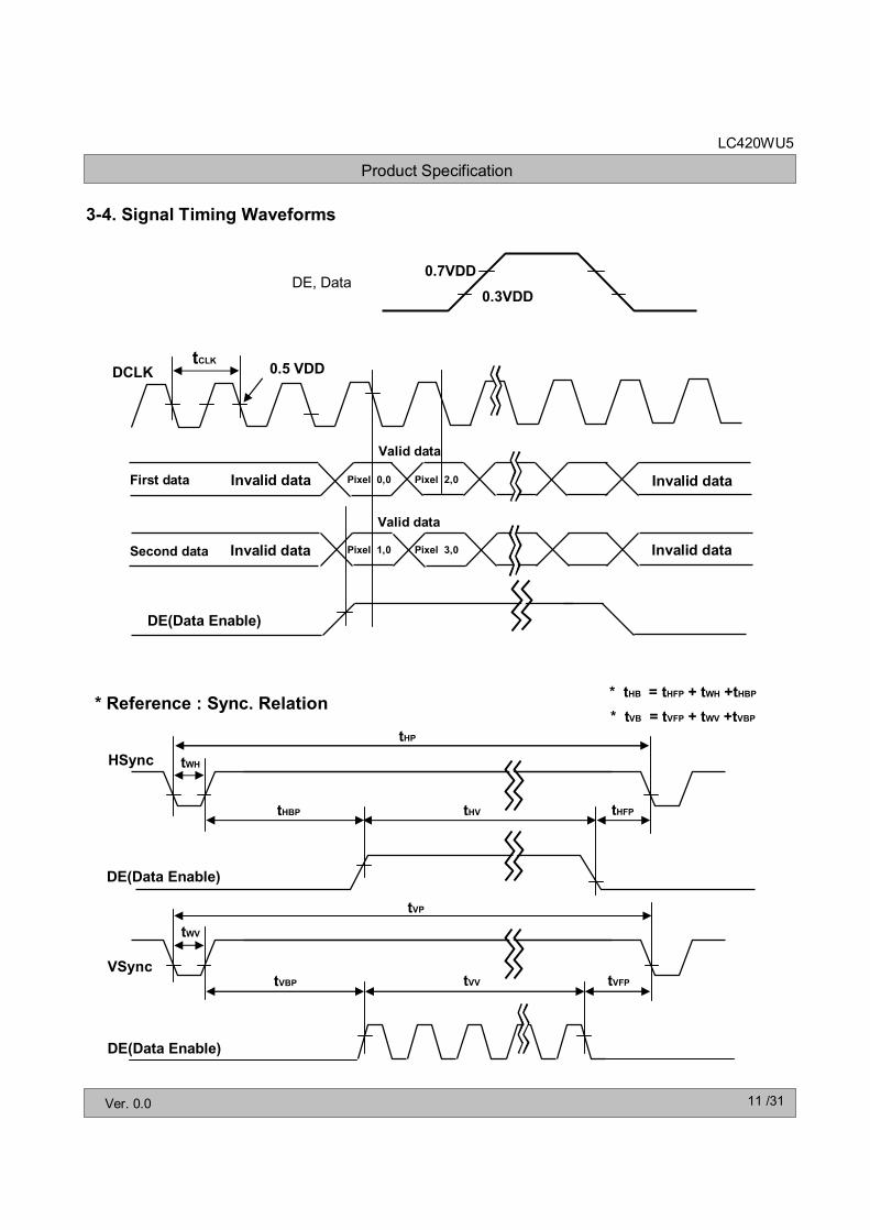
Table 6 shows the signal timing required at the input of the LVDS transmitter. All of the interface signal timing should be satisfied with the following specification for normal operation.
3-3. Signal Timing Specifications
Horizontal
Vertical Lines(69)45(11)tVBBlank
Lines-1080-tVVDisplay Period
Lines(1149)1125(1091)tVPTotal
Total
Blank
Display Period
tHP
tHB
tHV
Symbol
2200/2tclk(1280)1100(1060)
tclk(320)140(100)
tclk-960-
NoteUnitMaxTypMinITEM
Frequency
Vertical
Horizontal
DCLK
fV
fH
fCLK
Symbol
Hz(63)60(57)
KHz(68.9)67.5(65.5)
148.5/2MHz(77)74.25(71.55)
NoteUnitMaxTypMinITEM
Table 7. TIMING TABLE for PAL (DE Only Mode)
Note : The Input of HSYNC & VSYNC signal does not have an effect on normal operation(DE Only Mode).The performance of the electro-optical characteristics may be influenced by variance of the vertical refresh rate.
Table 7 shows the signal timing required at the input of the LVDS transmitter. All of the interface signal timing should be satisfied with the following specification for normal operation.
Horizontal
Vertical Lines(65)45(25)tVBBlank
Lines-1080-tVVDisplay Period
Lines(1145)1125(1105)tVPTotal
Total
Blank
Display Period
tHP
tHB
tHV
Symbol
2200/2tclk(1200)1100(1060)
tclk(240)140(100)
tclk-960-
NoteUnitMaxTypMinITEM
Frequency
Vertical
Horizontal
DCLK
fV
fH
fCLK
Symbol
Hz(51)50(49)
KHz(57.25)56.25(55.25)
123.75/2MHz(63.13)61.88(60.64)
NoteUnitMaxTypMinITEM
Product Specification
11 /31
LC420WU5
Ver. 0.0
0.7VDD
0.3VDD
tCLK
Invalid data
Valid data
Invalid data
Invalid data
Invalid data
Pixel 0,0 Pixel 2,0
Pixel 1,0 Pixel 3,0
DE(Data Enable)
Valid data
0.5 VDD
tHP
tHBP tHV tHFP
tVP
tWV
tVBP tVV tVFP
HSync
VSync
DE(Data Enable)
DE(Data Enable)
DCLK
First data
Second data
DE, Data
tWH
3-4. Signal Timing Waveforms
* Reference : Sync. Relation* tHB = tHFP + tWH +tHBP
* tVB = tVFP + tWV +tVBP

Product Specification
12 /31
LC420WU5
Ver. 0.0
The brightness of each primary color(red,green,blue) is based on the 8-bit gray scale data input for the color.The higher binary input, the brighter the color. Table 8 provides a reference for color versus data input.
Table 8. COLOR DATA REFERENCE
0 0 0 0 0 0 0 00 0 0 0 0 0 0 00 0 0 0 0 0 0 0GREEN (000) Dark
GREEN
0 0 0 0 0 0 0 00 0 0 0 0 0 0 10 0 0 0 0 0 0 0GREEN (001)
............
0 0 0 0 0 0 0 01 1 1 1 1 1 1 00 0 0 0 0 0 0 0GREEN (254)
0 0 0 0 0 0 0 01 1 1 1 1 1 1 10 0 0 0 0 0 0 0GREEN (255)
0 0 0 0 0 0 0 00 0 0 0 0 0 0 00 0 0 0 0 0 0 0RED (000) Dark
RED
0 0 0 0 0 0 0 00 0 0 0 0 0 0 00 0 0 0 0 0 0 1RED (001)
............
0 0 0 0 0 0 0 00 0 0 0 0 0 0 01 1 1 1 1 1 1 0RED (254)
0 0 0 0 0 0 0 00 0 0 0 0 0 0 01 1 1 1 1 1 1 1RED (255)
0 0 0 0 0 0 0 10 0 0 0 0 0 0 00 0 0 0 0 0 0 0BLUE (001)
............
1 1 1 1 1 1 1 00 0 0 0 0 0 0 00 0 0 0 0 0 0 0BLUE (254)
1 1 1 1 1 1 1 10 0 0 0 0 0 0 00 0 0 0 0 0 0 0BLUE (255)
BLUE (000) Dark
White
Yellow
Magenta
Cyan
Blue (255)
Green (255)
Red (255)
Black 0 0 0 0 0 0 0 00 0 0 0 0 0 0 00 0 0 0 0 0 0 0
BasicColor
0 0 0 0 0 0 0 00 0 0 0 0 0 0 01 1 1 1 1 1 1 1
0 0 0 0 0 0 0 01 1 1 1 1 1 1 10 0 0 0 0 0 0 0
1 1 1 1 1 1 1 10 0 0 0 0 0 0 00 0 0 0 0 0 0 0
1 1 1 1 1 1 1 11 1 1 1 1 1 1 10 0 0 0 0 0 0 0
1 1 1 1 1 1 1 10 0 0 0 0 0 0 01 1 1 1 1 1 1 1
0 0 0 0 0 0 0 01 1 1 1 1 1 1 11 1 1 1 1 1 1 1
1 1 1 1 1 1 1 11 1 1 1 1 1 1 11 1 1 1 1 1 1 1
BLUEMSB LSB
GREENMSB LSB
REDMSB LSB
B7 B6 B5 B4 B3 B2 B1 B0G7 G6 G5 G4 G3 G2 G1 G0R7 R6 R5 R4 R3 R2 R1 R0
0 0 0 0 0 0 0 00 0 0 0 0 0 0 00 0 0 0 0 0 0 0
BLUE
Color
Input Color Data
3-5. Color Data Reference
Product Specification
13 /31
LC420WU5
Ver. 0.0
3-6. Power Sequence
Note : 1. Please avoid floating state of interface signal at invalid period.2. When the interface signal is invalid, be sure to pull down the power supply VLCD to 0V.3. The case when the T2/T5 exceed 3x(1/fv), it operates protection pattern (Black pattern) till valid
signal inputted. There is no reliability problem. (ex. 60Hz : 3x(1/60Hz) = 50ms) 4. The T3/T4 is recommended value, the case when failed to meet a minimum specification,
abnormal display would be shown. There is no reliability problem.5. If the on time of signals(Interface signal and Option signals) precedes the on time of Power(VLCD),
check the LCD logic Power(Vcc) is under 0.8V, otherwise it will be happened abnormal display. 6. T6 should be measured after the Module has been fully discharged between power off and on
period.
-
T2
-
-
5
5
2,63,5
44
3,5
Notes
s--2.0T6
ms0T8
ms0T7
ms3 x (1/fV)-0.5T2
msms--200T3
--200T4
ms--0T5
ms20-0.5T1
MaxTypMinUnit
ValueParameter
Table 9. POWER SEQUENCE
Interface Signal (Tx)
Power for Lamp
Power Supply For LCDVLCD
10%0V
90%
10%
T1 T2 T5 T6
T3 T4
Valid Data
Lamp ON
T7 T8Option Signal (LVDS_select, DCR_Enable, BIT_select)
90%3-6-1. LCD Driving circuit

Product Specification
14 /31
LC420WU5
Ver. 0.0
3-6-2. Sequence for Inverter
Power Supply For Inverter
VON/OFF
VBL
10%0V
90%
T1 T2 T3 T2
0.7V
T4
24V (typ.)
T5
Lamp ON
T4
T7
1000ms (Min) 1000ms (Min)
Table 10. Power Sequence for Inverter
3-6-3. Deep condition for Inverter
VBL(Typ.) x 0.8
0 V
VBL : 24VT6
Notes : 1. T1 describes rising time of 0V to 24V and this parameter does not applied at restarting time. 2. T4(max) is less than T2.3. In T7 section, VBR-B is recommended 3.3V.
VBL(Typ) x 0.8ms10--T63ms--1000T7
-ms--10T5
2ms0T4
1
Remarks
ms--500T2ms--200T3
ms--20T1MaxTypMin
UnitsValues
Parameter
VBR-A & VBR-B

Product Specification
15 /31
LC420WU5
Ver. 0.0
LCD ModuleOptical Stage(x,y) Pritchard 880 orequivalent
50cmFIG. 1 Optical Characteristic Measurement Equipment and Method
Optical characteristics are determined after the unit has been ¡ON¡ and stable in a dark environment at 25¡ 2¡C. The values specified are at an approximate distance 50cm from the LCD surface at a viewing angle of Φ and θequal to 0 ¡.FIG. 1 shows additional information concerning the measurement equipment and method.
4. Optical Specification
Table 11. OPTICAL CHARACTERISTICSTa= 25¡ 2¡C, VLCD=12.0V, fV=60Hz, Dclk=148.5MHz VBR_A=1.65V, VBR_B=3.3V
31.3--5Pδ WHITE
1-1000700CR
Gray-to-Gray
--- 7Gray Scale
y axis, down (φ=270¡)y axis, up (φ=90¡)x axis, left (φ=180¡)x axis, right(φ=0¡)
--89θd--89θu--89θl
6degree
--89θr
Viewing Angle (CR>10)
WHITE
BLUE
GREEN
RED
( 0 . 613)Gy( 0 . 287)Gx
( 0 . 065)By( 0 . 144)Bx
0.292Wy0.279Wx
ms
( 0 . 343)Ry
Typ +0.03
( 0 . 640)
Typ-0.03
Rx
Color Coordinates [CIE1931]
4,585-G to GResponse TimeLuminance Variation
2cd/m2-500400LWHSurface Luminance, white
NoteUnit
Contrast RatioMaxTypMin
ValueSymbolParameter

Product Specification
16 /31
LC420WU5
Ver. 0.0
Notes :1. Contrast Ratio(CR) is defined mathematically as :CR(Contrast Ratio) = Maximum CRn (n=1, 2, 3, 4, 5)
Surface Luminance at position n with all white pixelsCRn =
Surface Luminance at position n with all black pixelsn = the Position number(1, 2, 3, 4, 5). For more information, see FIG 2.
2. Surface luminance are determined after the unit has been ¡ON¡ and 30min after lighting the backlight in a dark environment at 25¡ 2¡C. Surface luminance is the luminance value at center 1-point across the LCD surface 50cm from the surface with all pixels displaying white.For more information see the FIG. 2.
3. The variation in surface luminance , δ WHITE is defined as :δ WHITE(5P) = Maximum(Lon1,Lon2, Lon3, Lon4, Lon5) / Minimum(Lon1,Lon2, Lon3, Lon4, Lon5)
Where Lon1 to Lon5 are the luminance with all pixels displaying white at 5 locations . For more information, see the FIG. 2.
4. Response time is the time required for the display to transition from G(N) to G(M) (Rise Time, TrR) and from G(M) to G(N) (Decay Time, TrD). For additional information see the FIG. 3. (N<M)
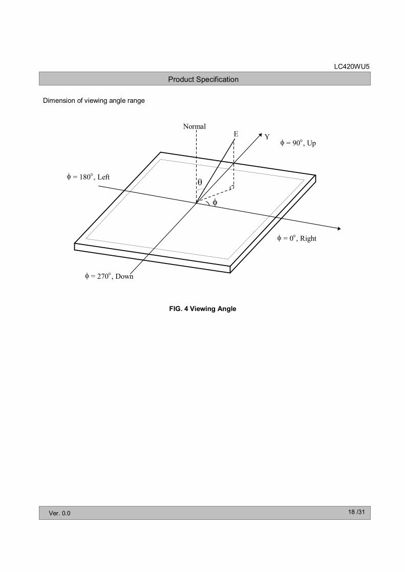
5. Viewing angle is the angle at which the contrast ratio is greater than 10. The angles aredetermined for the horizontal or x axis and the vertical or y axis with respect to the z axis whichis normal to the LCD module surface. For more information, see the FIG. 4.
6. Gray scale specificationGamma Value is approximately 2.2. For more information, see the Table 12.
Table 12. GRAY SCALE SPECIFICATION
100(86.7)(74.5)(63.3)(53.0)(43.8)(35.5)(28.2)(21.7)(16.2)(11.6)(7.77)(4.80)(2.61)(1.16)(0.39)(0.19)
Luminance [%] (Typ.)
L239L255
L159L175L191L207
L111L127L143
L223
L47L63L79L95
L31L15L0
Gray Level

Product Specification
17 /31
LC420WU5
Ver. 0.0
FIG. 3 Response Time
Response time is defined as the following figure and shall be measured by switching the input signal for ¡Gray(N)¡ and ¡Gray(M)¡.
Measuring point for surface luminance & measuring point for luminance variation.
FIG. 2 5 Points for Luminance Measure
A : H / 4 mmB : V / 4 mm@ H,V : Active Area
H
A
V
B
①
③②
⑤④
Gray(M)Gray(N)
TrR TrD10090
10
0
Optical Response
N,M = Black~White, N<MGray(N)
Product Specification
18 /31
LC420WU5
Ver. 0.0
FIG. 4 Viewing Angle
Dimension of viewing angle range
Normal Y E
φ
θ
φ = 0°, Right
φ = 180°, Left
φ = 270°, Down
φ = 90°, Up
Product Specification
19 /31
LC420WU5
Ver. 0.0
Table 13 provides general mechanical characteristics.
5. Mechanical Characteristics
Table 13. MECHANICAL CHARACTERISTICS
ValueItem
523.01 mmVertical
(11.5) Kg (Typ.) , (12.5) Kg (Max.)Weight
531.0 mmVertical
576.0 mmVertical
51.0 mmDepth
930.25 mmHorizontalActive Display Area
939.0 mmHorizontalBezel Area
983.0 mmHorizontal
Outline Dimension
Note : Please refer to a mechanic drawing in terms of tolerance at the next page.
Product Specification
20 /31
LC420WU5
Ver. 0.0
<FRONT VIEW>
Product Specification
21 /31
LC420WU5
Ver. 0.0
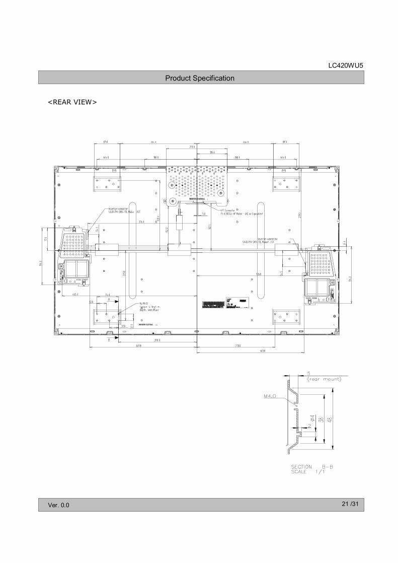
<REAR VIEW>
Product Specification
22 /31
LC420WU5
Ver. 0.0
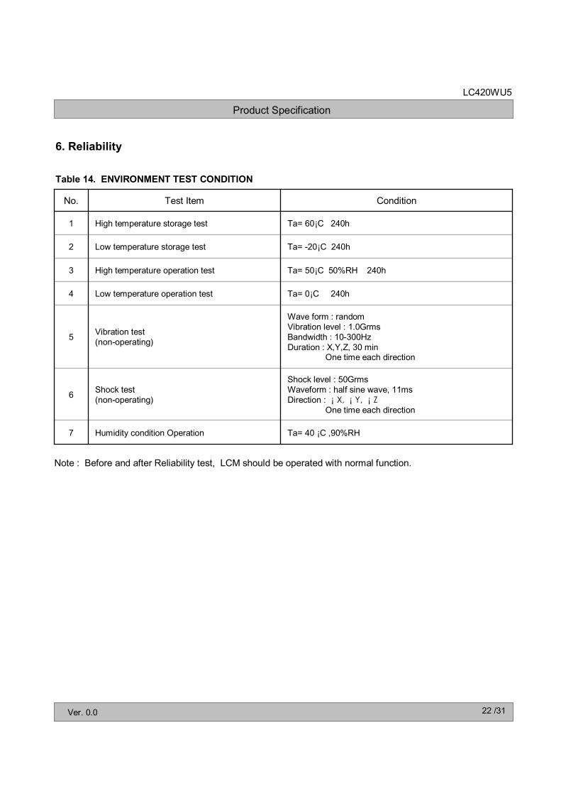
6. Reliability
Table 14. ENVIRONMENT TEST CONDITION
Ta= 40 ¡C ,90%RHHumidity condition Operation7
Shock level : 50GrmsWaveform : half sine wave, 11msDirection : ¡ X, ¡ Y, ¡ Z
One time each direction
Shock test(non-operating)6
Wave form : randomVibration level : 1.0GrmsBandwidth : 10-300HzDuration : X,Y,Z, 30 min
One time each direction
Vibration test(non-operating)5
Ta= 0¡C 240hLow temperature operation test4
Ta= 50¡C 50%RH 240hHigh temperature operation test3
Ta= -20¡C 240hLow temperature storage test2
Ta= 60¡C 240h High temperature storage test1
ConditionTest ItemNo.
Note : Before and after Reliability test, LCM should be operated with normal function.
Product Specification
23 /31
LC420WU5
Ver. 0.0
7. International Standards
7-1. Safety
a) UL 60065, 7th Edition, dated June 30, 2003, Underwriters Laboratories, Inc.,Standard for Audio, Video and Similar Electronic Apparatus.
b) CAN/CSA C22.2, No. 60065:03, Canadian Standards Association,Standard for Audio, Video and Similar Electronic Apparatus.
c) IEC60065:2001, 7th Edition CB-scheme and EN 60065:2002, Safety requirements for Audio, Video and Similar Electronic Apparatus..
7-2. EMCa) ANSI C63.4 ¡Methods of Measurement of Radio-Noise Emissions from Low-Voltage Electrical and
Electrical Equipment in the Range of 9kHZ to 40GHz. ¡American National Standards Institute(ANSI),1992
b) CISPR22 ¡Limits and Methods of Measurement of Radio Interface Characteristics of InformationTechnology Equipment.¡ International Special Committee on Radio Interference.
c) EN 55022 ¡Limits and Methods of Measurement of Radio Interface Characteristics of InformationTechnology Equipment.¡ European Committee for Electro technical Standardization.(CENELEC), 1998 ( Including A1: 2000 )

Product Specification
24 /31
LC420WU5
Ver. 0.0
8-1. Designation of Lot Marka) Lot Mark
A B C D E F G H I J K L M
A,B,C : SIZE(INCH)D : YEAR E : MONTHF : PANEL CODE G : FACTORY CODEH : ASSEMBLY CODE I,J,K,L,M : SERIAL NO.
Note1. YEAR
b) Location of Lot Mark
2. MONTH
Serial NO. is printed on the label. The label is attached to the backside of the LCD module.This is subject to change without prior notice.
8-2. Packing Forma) Package quantity in one Pallet : 12 pcs
b) Pallet Size : 1150 mm X 1020 mm X 815 mm.
B
Nov
Mark
Month
A
Oct
6
Jun
7
Jul
8
Aug
9
Sep
4
Apr
5
May
C421
DecMarFebJan
8. Packing
Mark
Year
0
2010
6
2006
7
2007
8
2008
9
2009
4
2004
5
2005
321
200320022001

Product Specification
25 /31
LC420WU5
Ver. 0.0
Please pay attention to the followings when you use this TFT LCD module.
9-1. Mounting Precautions(1) You must mount a module using specified mounting holes (Details refer to the drawings).(2) You should consider the mounting structure so that uneven force (ex. Twisted stress) is not applied to the
module. And the case on which a module is mounted should have sufficient strength so that external force is not transmitted directly to the module.
(3) Please attach the surface transparent protective plate to the surface in order to protect the polarizer.Transparent protective plate should have sufficient strength in order to the resist external force.
(4) You should adopt radiation structure to satisfy the temperature specification.(5) Acetic acid type and chlorine type materials for the cover case are not desirable because the former
generates corrosive gas of attacking the polarizer at high temperature and the latter causes circuit break by electro-chemical reaction.
(6) Do not touch, push or rub the exposed polarizers with glass, tweezers or anything harder than HBpencil lead. And please do not rub with dust clothes with chemical treatment.Do not touch the surface of polarizer for bare hand or greasy cloth.(Some cosmetics are detrimentalto the polarizer.)
(7) When the surface becomes dusty, please wipe gently with absorbent cotton or other soft materials like chamois soaks with petroleum benzine. Normal-hexane is recommended for cleaning the adhesives used to attach front / rear polarizers. Do not use acetone, toluene and alcohol because they cause chemical damage to the polarizer.
(8) Wipe off saliva or water drops as soon as possible. Their long time contact with polarizer causes deformations and color fading.
(9) Do not open the case because inside circuits do not have sufficient strength.
9-2. Operating Precautions
9. Precautions
(1) The spike noise causes the mis-operation of circuits. It should be lower than following voltage : V=¡ 200mV(Over and under shoot voltage)
(2) Response time depends on the temperature.(In lower temperature, it becomes longer.)(3) Brightness depends on the temperature. (In lower temperature, it becomes lower.)
And in lower temperature, response time(required time that brightness is stable after turned on) becomes longer
(4) Be careful for condensation at sudden temperature change.Condensation makes damage to polarizer or electrical contacted parts. And after fading condensation, smear or spot will occur.
(5) When fixed patterns are displayed for a long time, remnant image is likely to occur.(6) Module has high frequency circuits. Sufficient suppression to the electromagnetic interference shall be
done by system manufacturers. Grounding and shielding methods may be important to minimized theinterference.
(7) Please do not give any mechanical and/or acoustical impact to LCM. Otherwise, LCM can¡t be operated its full characteristics perfectly.
(8) A screw which is fastened up the steels should be a machine screw. (if not, it can causes conductive particles and deal LCM a fatal blow)
(9) Please do not set LCD on its edge.(10) It is recommended to avoid the signal cable and conductive material over the inverter transformer
for it can cause the abnormal display and temperature rising.
Product Specification
26 /31
LC420WU5
Ver. 0.0
Since a module is composed of electronic circuits, it is not strong to electrostatic discharge. Make certain that treatment persons are connected to ground through wrist band etc. And don¡t touch interface pin directly.
9-3. Electrostatic Discharge Control
Strong light exposure causes degradation of polarizer and color filter.
9-4. Precautions for Strong Light Exposure
When storing modules as spares for a long time, the following precautions are necessary.
(1) Store them in a dark place. Do not expose the module to sunlight or fluorescent light. Keep the temperature between 5¡C and 35¡C at normal humidity.
(2) The polarizer surface should not come in contact with any other object.It is recommended that they be stored in the container in which they were shipped.
9-5. Storage
9-6. Handling Precautions for Protection Film(1) The protection film is attached to the bezel with a small masking tape.
When the protection film is peeled off, static electricity is generated between the film and polarizer.This should be peeled off slowly and carefully by people who are electrically grounded and with well ion-blown equipment or in such a condition, etc.
(2) When the module with protection film attached is stored for a long time, sometimes there remains a very small amount of glue still on the bezel after the protection film is peeled off.
(3) You can remove the glue easily. When the glue remains on the bezel surface or its vestige is recognized, please wipe them off with absorbent cotton waste or other soft material like chamois soaked with normal-hexane.
Product Specification
27 /31
LC420WU5
Ver. 0.0
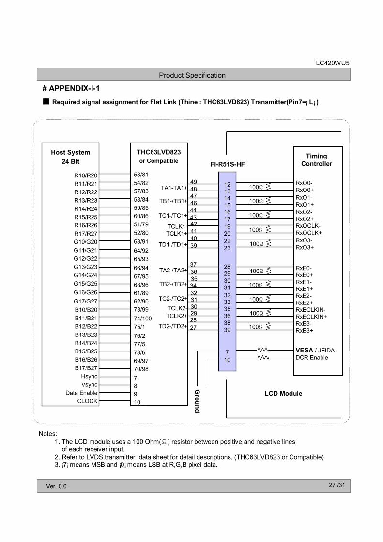
R10/R20R11/R21R12/R22R13/R23R14/R24R15/R25R16/R26R17/R27G10/G20G11/G21G12/G22G13/G23G14/G24G15/G25G16/G26G17/G27B10/B20B11/B21B12/B22B13/B23B14/B24B15/B25B16/B26B17/B27
HsyncVsync
Data EnableCLOCK
Host System24 Bit
TA1-TA1+
TB1-/TB1+
TC1-/TC1+
TCLK1-TCLK1+
TD1-/TD1+
TA2-/TA2+
TB2-/TB2+
TC2-/TC2+ TCLK2-TCLK2+
TD2-/TD2+
THC63LVD823or Compatible
RxO0-RxO0+RxO1-RxO1+RxO2-RxO2+RxOCLK-RxOCLK+RxO3-RxO3+
RxE0-RxE0+RxE1-RxE1+RxE2-RxE2+RxECLKIN-RxECLKIN+RxE3-RxE3+
VESA / JEIDA DCR Enable
FI-R51S-HFTiming
Controller
LCD Module
Ground
49484746
4039
44434241
37
35
3130
36
3432
292827
100Ω
100Ω
100Ω
100Ω
100Ω
100Ω
100Ω
100Ω
100Ω
100Ω
12131415161719202223
28293031323335363839
710
53/8154/8257/8358/8459/8560/8651/7952/8063/9164/9265/9366/9467/9568/9661/8962/9073/9974/10075/176/277/578/669/9770/9878910
# APPENDIX-I-1 Required signal assignment for Flat Link (Thine : THC63LVD823) Transmitter(Pin7=¡ L¡ )
Notes: 1. The LCD module uses a 100 Ohm(Ω) resistor between positive and negative lines
of each receiver input.2. Refer to LVDS transmitter data sheet for detail descriptions. (THC63LVD823 or Compatible)3. ¡7¡ means MSB and ¡0¡ means LSB at R,G,B pixel data.

Product Specification
28 /31
LC420WU5
Ver. 0.0
R10/R20R11/R21R12/R22R13/R23R14/R24R15/R25R16/R26R17/R27G10/G20G11/G21G12/G22G13/G23G14/G24G15/G25G16/G26G17/G27B10/B20B11/B21B12/B22B13/B23B14/B24B15/B25B16/B26B17/B27
HsyncVsync
Data EnableCLOCK
Host System24 Bit
THC63LVD823or Compatible
51/7952/8053/8154/8257/8358/8459/8560/8661/8962/9063/9164/9265/9366/9467/9568/9669/9770/9873/9974/10075/176/277/578/678910
TA1-TA1+
TB1-/TB1+
TC1-/TC1+
TCLK1-TCLK1+
TD1-/TD1+
TA2-/TA2+
TB2-/TB2+
TC2-/TC2+ TCLK2-TCLK2+
TD2-/TD2+
RxO0-RxO0+RxO1-RxO1+RxO2-RxO2+RxOCLK-RxOCLK+RxO3-RxO3+
RxE0-RxE0+RxE1-RxE1+RxE2-RxE2+RxECLKIN-RxECLKIN+RxE3-RxE3+
VESA / JEIDADCR Enable
FI-R51S-HFTiming
Controller
LCD Module VCC
49484746
4039
44434241
37
35
3130
36
3432
292827
100Ω
100Ω
100Ω
100Ω
100Ω
100Ω
100Ω
100Ω
100Ω
100Ω
12131415161719202223
28293031323335363839
710
# APPENDIX-I-2 Required signal assignment for Flat Link (Thine : THC63LVD823) Transmitter(Pin7=¡ H¡ )
Notes: 1. The LCD module uses a 100 Ohm(Ω) resistor between positive and negative lines
of each receiver input.2. Refer to LVDS transmitter data sheet for detail descriptions. (THC63LVD823 or Compatible)3. ¡7¡ means MSB and ¡0¡ means LSB at R,G,B pixel data.

Product Specification
29 /31
LC420WU5
Ver. 0.0
# APPENDIX-II Pallet Ass¡y
STEELBAND,CLIP9
PPBAND10
YUPO 80G 100X100LABEL11
PAPERANGLE,PACKING8
PAPER 1140X990X130MMPALLET4
MASKING 20MMX50MTAPE3
EPSPACKING,TOP6
EPSPACKING,BOTTOM5
PAPER ANGLE,POST7
42INCHBAG2
LCD Module1
MATERIALDESCRIPTIONNO.
Product Specification
30 /31
LC420WU5
Ver. 0.0
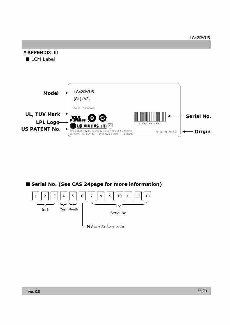
# APPENDIX 2# APPENDIX- III LCM Label
8
Serial No. (See CAS 24page for more information)
1 2 3 4 5 6 7 9 10 11 12
Inch
M Ass¡y Factory code
Serial No.
13
MonthYear
Model
Serial No.UL, TUV Mark
LPL LogoUS PATENT No. Origin
LC420WU5
(SL) (A2)

Product Specification
31 /31
LC420WU5
Ver. 0.0
# APPENDIX 3# APPENDIX- IV Pallet Label
LC420WU5SLA2
12 PCS 001/01-01
MADE IN KOREA RoHS Verified
XXXXX XXXXXXXX XXX XXX XXXX