Embed Size (px)
Citation preview
Solid immersion lens applications for nanophotonic devices
Keith A. Serrels,a Euan Ramsay,b Paul A. Dalgarno,c Brian D.
Gerardot,c John A. O’Connor,d Robert H. Hadfield,d Richard J. Warburton,c and Derryck T. Reida
a Ultrafast Optics Group, b Waves and Fields Group,
c Nano-Optics Group, d Superconducting Single-Photon Detectors Group,
School of Engineering and Physical Sciences, Heriot-Watt University, Riccarton, Edinburgh EH14 4AS, UK
Abstract. Solid immersion lens (SIL) microscopy combines the advantages of conventional microscopy with those of near-field techniques, and is being increasingly adopted across a diverse range of technologies and applications. A comprehensive overview of the state-of-the-art in this rapidly expanding subject is therefore increasingly relevant. Important benefits are enabled by SIL-focusing, including an improved lateral and axial spatial profiling resolution when a SIL is used in laser-scanning microscopy or excitation, and an improved collection efficiency when a SIL is used in a light-collection mode, for example in fluorescence micro-spectroscopy. These advantages arise from the increase in numerical aperture (NA) that is provided by a SIL. Other SIL-enhanced improvements, for example spherical-aberration-free sub-surface imaging, are a fundamental consequence of the aplanatic imaging condition that results from the spherical geometry of the SIL. The theory of SIL imaging exposes the unique properties of SILs that provide advantages in applications involving the interrogation of photonic and electronic nanostructures. Such applications range from the sub-surface examination of the complex three-dimensional microstructures fabricated in silicon integrated circuits, to quantum photoluminescence and transmission measurements in semiconductor quantum dot nanostructures. Keywords: solid immersion lens, semiconductor, integrated-circuit inspection, optical data storage, photoresponse mapping, nanoscale spectroscopy, optical super-resolution. 1 INTRODUCTION The solid immersion lens (SIL) is a powerful optical component which plays an important enabling role in a variety of nanophotonic applications. Since its invention, the SIL has been exploited in several nanoscale technologies, including semiconductor integrated-circuit (IC) inspection [1-3], nanoscale spectroscopy [4, 5], optical data storage [6, 7] and photolithography [8], yet the benefits the SIL has introduced in these fields have received poor coverage. Therefore, in this paper we aim to review the theoretical aspects of the SIL and to discuss recent demonstrations of SIL-enhanced technologies in nanophotonics.
In the field of nanophotonics, optical experiments are carried out with a spatial resolution of a few hundred nanometers or less. These near-field investigations demand the utmost precision, and draw on a wide range of optical techniques, typically requiring state-of-the-art equipment and complex optical arrangements. In contrast, a SIL is a remarkably simple optical component, which is straightforward to introduce and use. A well-defined list of progressive developments can be realized via the use of a SIL: SIL-enhanced methodologies offer improvements in spatial resolution (resolving power), collection efficiency and magnification, all critical parameters in the investigation of nanoscale devices. All these parameters will be discussed in detail later in this paper.
Journal of Nanophotonics, Vol. 2, 021854 (19 December 2008)
© 2008 Society of Photo-Optical Instrumentation Engineers [DOI: 10.1117/1.3068652]Received 22 Sep 2008; accepted 12 Dec 2008; published 19 Dec 2008 [CCC: 19342608/2008/$25.00]Journal of Nanophotonics, Vol. 2, 021854 (2008) Page 1
Downloaded From: http://nanophotonics.spiedigitallibrary.org/ on 09/10/2013 Terms of Use: http://spiedl.org/terms
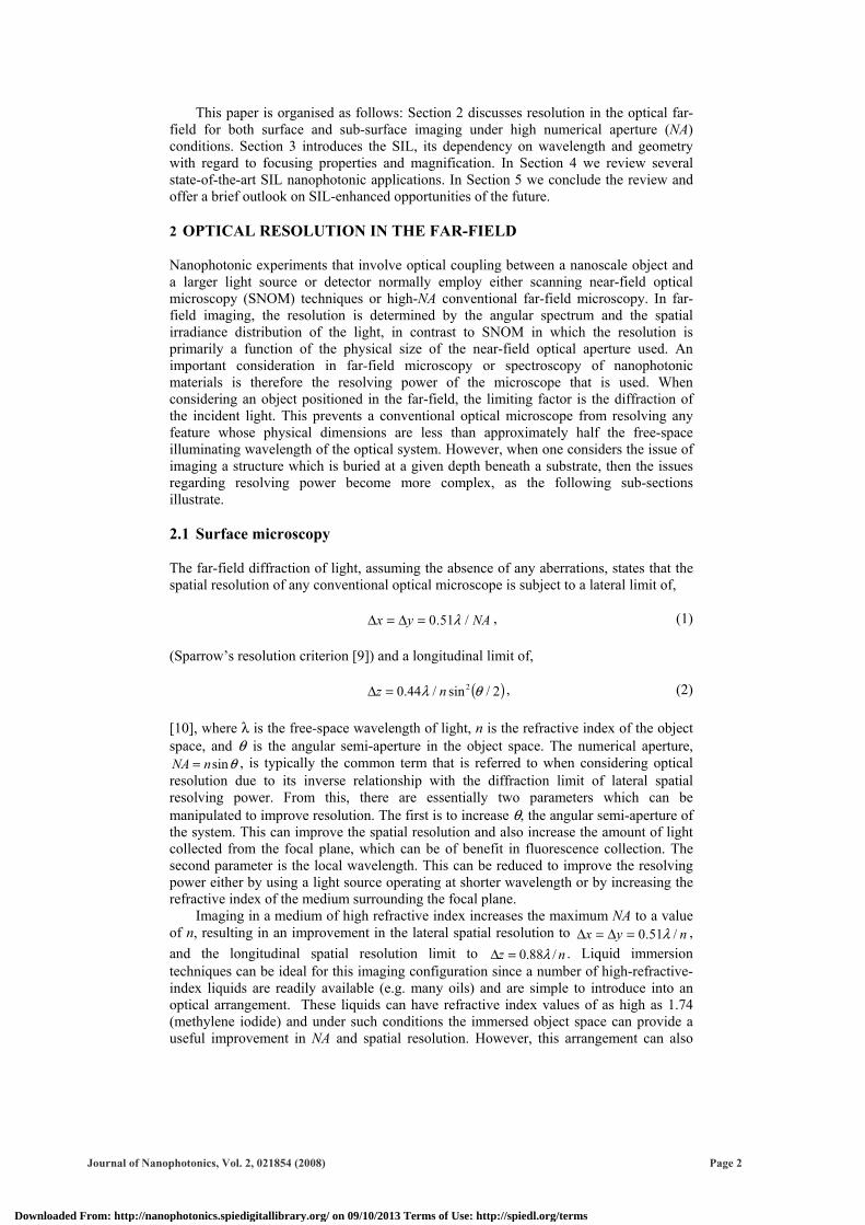
This paper is organised as follows: Section 2 discusses resolution in the optical far-field for both surface and sub-surface imaging under high numerical aperture (NA) conditions. Section 3 introduces the SIL, its dependency on wavelength and geometry with regard to focusing properties and magnification. In Section 4 we review several state-of-the-art SIL nanophotonic applications. In Section 5 we conclude the review and offer a brief outlook on SIL-enhanced opportunities of the future.
2 OPTICAL RESOLUTION IN THE FAR-FIELD Nanophotonic experiments that involve optical coupling between a nanoscale object and a larger light source or detector normally employ either scanning near-field optical microscopy (SNOM) techniques or high-NA conventional far-field microscopy. In far-field imaging, the resolution is determined by the angular spectrum and the spatial irradiance distribution of the light, in contrast to SNOM in which the resolution is primarily a function of the physical size of the near-field optical aperture used. An important consideration in far-field microscopy or spectroscopy of nanophotonic materials is therefore the resolving power of the microscope that is used. When considering an object positioned in the far-field, the limiting factor is the diffraction of the incident light. This prevents a conventional optical microscope from resolving any feature whose physical dimensions are less than approximately half the free-space illuminating wavelength of the optical system. However, when one considers the issue of imaging a structure which is buried at a given depth beneath a substrate, then the issues regarding resolving power become more complex, as the following sub-sections illustrate. 2.1 Surface microscopy The far-field diffraction of light, assuming the absence of any aberrations, states that the spatial resolution of any conventional optical microscope is subject to a lateral limit of,
NAyx /51.0 λ=∆=∆ , (1)
(Sparrow’s resolution criterion [9]) and a longitudinal limit of,
( )2/sin/44.0 2 θλ nz =∆ , (2) [10], where λ is the free-space wavelength of light, n is the refractive index of the object space, and θ is the angular semi-aperture in the object space. The numerical aperture,
θsinnNA = , is typically the common term that is referred to when considering optical resolution due to its inverse relationship with the diffraction limit of lateral spatial resolving power. From this, there are essentially two parameters which can be manipulated to improve resolution. The first is to increase θ, the angular semi-aperture of the system. This can improve the spatial resolution and also increase the amount of light collected from the focal plane, which can be of benefit in fluorescence collection. The second parameter is the local wavelength. This can be reduced to improve the resolving power either by using a light source operating at shorter wavelength or by increasing the refractive index of the medium surrounding the focal plane.
Imaging in a medium of high refractive index increases the maximum NA to a value of n, resulting in an improvement in the lateral spatial resolution to nyx /51.0 λ=∆=∆ , and the longitudinal spatial resolution limit to nz /88.0 λ=∆ . Liquid immersion techniques can be ideal for this imaging configuration since a number of high-refractive-index liquids are readily available (e.g. many oils) and are simple to introduce into an optical arrangement. These liquids can have refractive index values of as high as 1.74 (methylene iodide) and under such conditions the immersed object space can provide a useful improvement in NA and spatial resolution. However, this arrangement can also
Journal of Nanophotonics, Vol. 2, 021854 (2008) Page 2
Downloaded From: http://nanophotonics.spiedigitallibrary.org/ on 09/10/2013 Terms of Use: http://spiedl.org/terms
introduce deleterious effects. An example of this is an increased probability of dirt and debris in the liquid entering the object space. This will contaminate both the immersion liquid and the sample under inspection.
2.2 Sub-surface microscopy When the object space is located at a given depth below the surface of a material then a range of issues are encountered that determine whether these buried structures can be adequately resolved by an optical microscope. The first consideration concerns the optical transparency of the surrounding medium. This parameter will determine the range of illumination wavelengths that are suitable to use, since light must be able to travel through the bulk material with sufficiently low loss in order to reach the buried features, and (in reflectance microscopy) to travel back through the sample towards the objective lens. Another parameter of critical importance is the refractive index. This value determines how the incident light will be reflected and refracted at the surface of the medium.
In the commonly encountered case of a planar air-medium interface, reflection from the surface will reduce the amount of light which can be coupled into the material, limiting the amount of light that can be collected by a microscope objective to rays propagating at angles of incidence below the critical angle, ( )nc /1sin 1−=θ . For these rays, Snell’s Law informs us that in a sub-surface configuration the angular semi-aperture in the medium is reduced by a factor of n. Despite this reduction in the local value of
θsin , the overall NA of the imaging system remains unchanged because the refractive index in the object space is proportionately greater than that in air.
Another effect that refraction has on limiting optimum resolution achievable below a planar air-medium interface is that it introduces a significant amount of spherical aberration. This has a considerable effect on the diffraction limited performance of the microscope since spherical aberration increases linearly with angle and it is exactly these high-NA rays which one must include to obtain optimum resolving power.
Historically, liquid immersion techniques have been applied to circumvent some of these limiting factors by mitigating the effect of the planar geometry of the air-medium interface in order to improve the sub-surface resolving power of a microscope. Without any correction, the refractive effects described above ultimately mean a sub-surface imaging arrangement will always produce poorer performance than an imaging arrangement at the surface unless the planar interface geometry can be suitably modified. 3 THE SOLID IMMERSION LENS Solid immersion microscopy was invented by Mansfield and Kino in 1990 [11, 12] and since then has generated an increasing level of interest, particularly in the field of nanophotonics. It is based on the previously discussed idea of liquid immersion microscopy [13] but improves on this technique by including the light that is located beyond the critical angle in the system to enhance the spatial resolution and beam-collection efficiency.
SIL methods are well suited to the imaging, characterization and even the fabrication of many photonic nanostructure devices [14-17] since it is not possible to obtain any suitable immersion oils that have refractive indices approaching those of common semiconductors, nor is it possible to physically immerse the objective lens into solid samples.
Two types of SIL design are available and are discussed in detail below. 3.1 Hemispherical solid immersion lenses The SIL concept comes from the theory described by Born and Wolf [10]. This theory states that light can be focused without aberrations at only two points within a high-index sphere. These focal points are known as the “aplanatic” points of the sphere.
Journal of Nanophotonics, Vol. 2, 021854 (2008) Page 3
Downloaded From: http://nanophotonics.spiedigitallibrary.org/ on 09/10/2013 Terms of Use: http://spiedl.org/terms
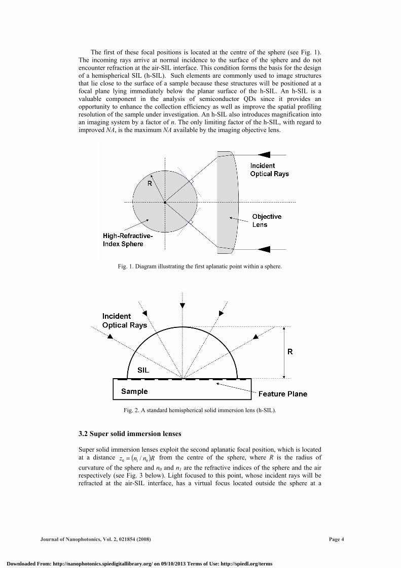
The first of these focal positions is located at the centre of the sphere (see Fig. 1). The incoming rays arrive at normal incidence to the surface of the sphere and do not encounter refraction at the air-SIL interface. This condition forms the basis for the design of a hemispherical SIL (h-SIL). Such elements are commonly used to image structures that lie close to the surface of a sample because these structures will be positioned at a focal plane lying immediately below the planar surface of the h-SIL. An h-SIL is a valuable component in the analysis of semiconductor QDs since it provides an opportunity to enhance the collection efficiency as well as improve the spatial profiling resolution of the sample under investigation. An h-SIL also introduces magnification into an imaging system by a factor of n. The only limiting factor of the h-SIL, with regard to improved NA, is the maximum NA available by the imaging objective lens.
Fig. 1. Diagram illustrating the first aplanatic point within a sphere.
Fig. 2. A standard hemispherical solid immersion lens (h-SIL).
3.2 Super solid immersion lenses Super solid immersion lenses exploit the second aplanatic focal position, which is located at a distance ( )Rnnz 010 /= from the centre of the sphere, where R is the radius of curvature of the sphere and n0 and n1 are the refractive indices of the sphere and the air respectively (see Fig. 3 below). Light focused to this point, whose incident rays will be refracted at the air-SIL interface, has a virtual focus located outside the sphere at a
Journal of Nanophotonics, Vol. 2, 021854 (2008) Page 4
Downloaded From: http://nanophotonics.spiedigitallibrary.org/ on 09/10/2013 Terms of Use: http://spiedl.org/terms
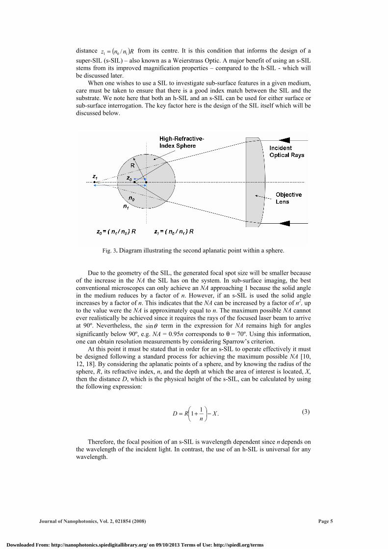
distance ( )Rnnz 101 /= from its centre. It is this condition that informs the design of a super-SIL (s-SIL) – also known as a Weierstrass Optic. A major benefit of using an s-SIL stems from its improved magnification properties – compared to the h-SIL - which will be discussed later. When one wishes to use a SIL to investigate sub-surface features in a given medium, care must be taken to ensure that there is a good index match between the SIL and the substrate. We note here that both an h-SIL and an s-SIL can be used for either surface or sub-surface interrogation. The key factor here is the design of the SIL itself which will be discussed below.
Fig. 3. Diagram illustrating the second aplanatic point within a sphere.
Due to the geometry of the SIL, the generated focal spot size will be smaller because of the increase in the NA the SIL has on the system. In sub-surface imaging, the best conventional microscopes can only achieve an NA approaching 1 because the solid angle in the medium reduces by a factor of n. However, if an s-SIL is used the solid angle increases by a factor of n. This indicates that the NA can be increased by a factor of n2, up to the value were the NA is approximately equal to n. The maximum possible NA cannot ever realistically be achieved since it requires the rays of the focused laser beam to arrive at 90º. Nevertheless, the θsin term in the expression for NA remains high for angles significantly below 90º, e.g. NA = 0.95n corresponds to θ = 70º. Using this information, one can obtain resolution measurements by considering Sparrow’s criterion.
At this point it must be stated that in order for an s-SIL to operate effectively it must be designed following a standard process for achieving the maximum possible NA [10, 12, 18]. By considering the aplanatic points of a sphere, and by knowing the radius of the sphere, R, its refractive index, n, and the depth at which the area of interest is located, X, then the distance D, which is the physical height of the s-SIL, can be calculated by using the following expression: .11 X
nRD −⎟
⎠⎞
⎜⎝⎛ += (3)
Therefore, the focal position of an s-SIL is wavelength dependent since n depends on the wavelength of the incident light. In contrast, the use of an h-SIL is universal for any wavelength.
Journal of Nanophotonics, Vol. 2, 021854 (2008) Page 5
Downloaded From: http://nanophotonics.spiedigitallibrary.org/ on 09/10/2013 Terms of Use: http://spiedl.org/terms
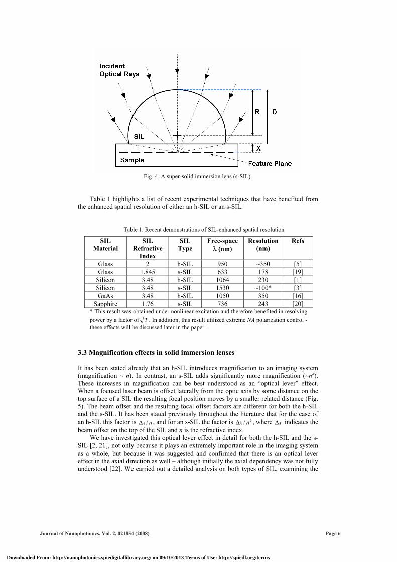
Fig. 4. A super-solid immersion lens (s-SIL).
Table 1 highlights a list of recent experimental techniques that have benefited from the enhanced spatial resolution of either an h-SIL or an s-SIL.
Table 1. Recent demonstrations of SIL-enhanced spatial resolution
SIL Material
SIL Refractive
Index
SIL Type
Free-space λ (nm)
Resolution (nm)
Refs
Glass 2 h-SIL 950 ~350 [5] Glass 1.845 s-SIL 633 178 [19]
Silicon 3.48 h-SIL 1064 230 [1] Silicon 3.48 s-SIL 1530 ~100* [3] GaAs 3.48 h-SIL 1050 350 [16]
Sapphire 1.76 s-SIL 736 243 [20] * This result was obtained under nonlinear excitation and therefore benefited in resolving power by a factor of 2 . In addition, this result utilized extreme NA polarization control - these effects will be discussed later in the paper.
3.3 Magnification effects in solid immersion lenses It has been stated already that an h-SIL introduces magnification to an imaging system (magnification ~ n). In contrast, an s-SIL adds significantly more magnification (~n2). These increases in magnification can be best understood as an “optical lever” effect. When a focused laser beam is offset laterally from the optic axis by some distance on the top surface of a SIL the resulting focal position moves by a smaller related distance (Fig. 5). The beam offset and the resulting focal offset factors are different for both the h-SIL and the s-SIL. It has been stated previously throughout the literature that for the case of an h-SIL this factor is nx /∆ , and for an s-SIL the factor is 2/ nx∆ , where x∆ indicates the beam offset on the top of the SIL and n is the refractive index.
We have investigated this optical lever effect in detail for both the h-SIL and the s-SIL [2, 21], not only because it plays an extremely important role in the imaging system as a whole, but because it was suggested and confirmed that there is an optical lever effect in the axial direction as well – although initially the axial dependency was not fully understood [22]. We carried out a detailed analysis on both types of SIL, examining the
Journal of Nanophotonics, Vol. 2, 021854 (2008) Page 6
Downloaded From: http://nanophotonics.spiedigitallibrary.org/ on 09/10/2013 Terms of Use: http://spiedl.org/terms
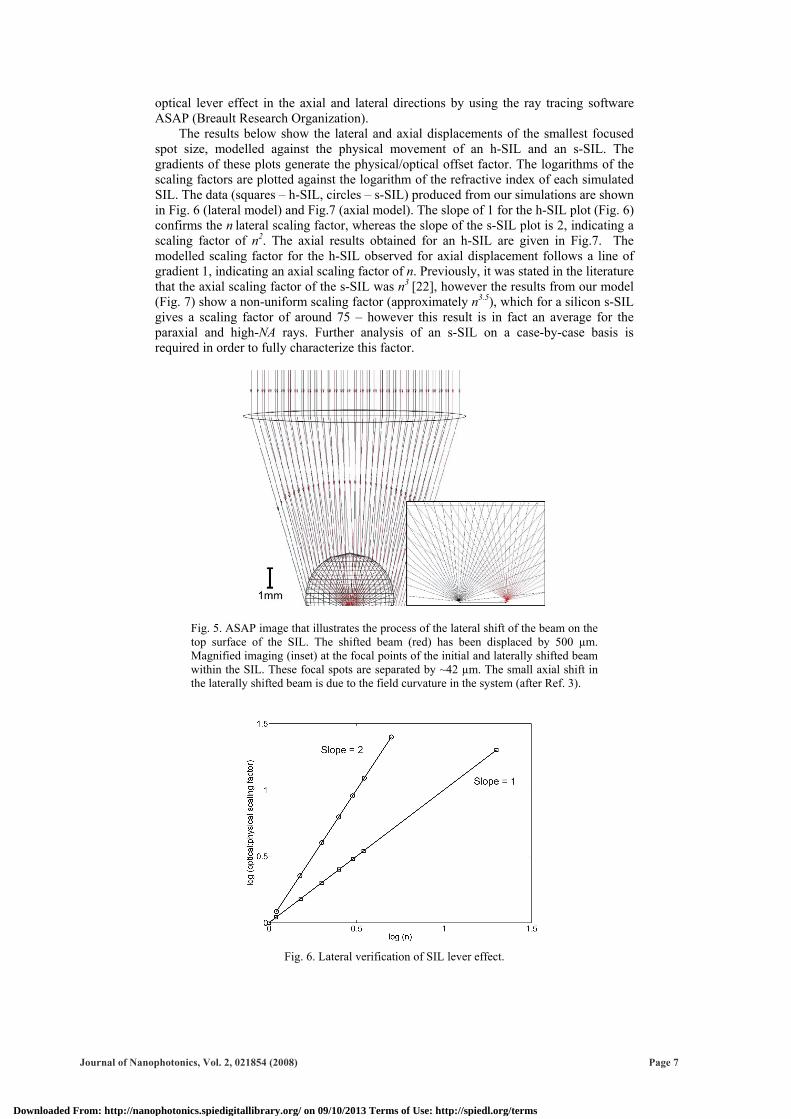
optical lever effect in the axial and lateral directions by using the ray tracing software ASAP (Breault Research Organization).
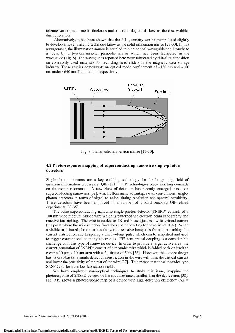
The results below show the lateral and axial displacements of the smallest focused spot size, modelled against the physical movement of an h-SIL and an s-SIL. The gradients of these plots generate the physical/optical offset factor. The logarithms of the scaling factors are plotted against the logarithm of the refractive index of each simulated SIL. The data (squares – h-SIL, circles – s-SIL) produced from our simulations are shown in Fig. 6 (lateral model) and Fig.7 (axial model). The slope of 1 for the h-SIL plot (Fig. 6) confirms the n lateral scaling factor, whereas the slope of the s-SIL plot is 2, indicating a scaling factor of n2. The axial results obtained for an h-SIL are given in Fig.7. The modelled scaling factor for the h-SIL observed for axial displacement follows a line of gradient 1, indicating an axial scaling factor of n. Previously, it was stated in the literature that the axial scaling factor of the s-SIL was n3 [22], however the results from our model (Fig. 7) show a non-uniform scaling factor (approximately n3.5), which for a silicon s-SIL gives a scaling factor of around 75 – however this result is in fact an average for the paraxial and high-NA rays. Further analysis of an s-SIL on a case-by-case basis is required in order to fully characterize this factor.
Fig. 5. ASAP image that illustrates the process of the lateral shift of the beam on the top surface of the SIL. The shifted beam (red) has been displaced by 500 µm. Magnified imaging (inset) at the focal points of the initial and laterally shifted beam within the SIL. These focal spots are separated by ~42 µm. The small axial shift in the laterally shifted beam is due to the field curvature in the system (after Ref. 3).
Fig. 6. Lateral verification of SIL lever effect.
Journal of Nanophotonics, Vol. 2, 021854 (2008) Page 7
Downloaded From: http://nanophotonics.spiedigitallibrary.org/ on 09/10/2013 Terms of Use: http://spiedl.org/terms
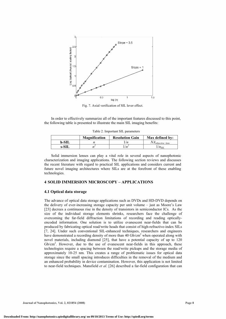
Fig. 7. Axial verification of SIL lever effect.
In order to effectively summarize all of the important features discussed to this point, the following table is presented to illustrate the main SIL imaging benefits:
Table 2. Important SIL parameters
Magnification Resolution Gain Max defined by: h-SIL n 1/n NAobjective lens s-SIL n2 1/n2 1/nSIL
Solid immersion lenses can play a vital role in several aspects of nanophotonic
characterization and imaging applications. The following section reviews and discusses the recent literature with regard to practical SIL applications and considers current and future novel imaging architectures where SILs are at the forefront of these enabling technologies. 4 SOLID IMMERSION MICROSCOPY – APPLICATIONS 4.1 Optical data storage The advance of optical data storage applications such as DVDs and HD-DVD depends on the delivery of ever-increasing storage capacity per unit volume – just as Moore’s Law [23] decrees a continuous rise in the density of transistors in semiconductor ICs. As the size of the individual storage elements shrinks, researchers face the challenge of overcoming the far-field diffraction limitations of recording and reading optically-encoded information. One solution is to utilize evanescent near-fields that can be produced by fabricating optical read/write heads that consist of high-refractive-index SILs [7, 24]. Under such conventional SIL-enhanced techniques, researchers and engineers have demonstrated a recording density of more than 40 Gb/cm2 when operated along with novel materials, including diamond [25], that have a potential capacity of up to 120 Gb/cm2. However, due to the use of evanescent near-fields in this approach, these technologies require a spacing between the read/write pickups and the storage media of approximately 10-25 nm. This creates a range of problematic issues for optical data storage since the small spacing introduces difficulties in the removal of the medium and an enhanced probability in device contamination. However, this application is not limited to near-field techniques. Mansfield et al. [26] described a far-field configuration that can
Journal of Nanophotonics, Vol. 2, 021854 (2008) Page 8
Downloaded From: http://nanophotonics.spiedigitallibrary.org/ on 09/10/2013 Terms of Use: http://spiedl.org/terms
tolerate variations in media thickness and a certain degree of skew as the disc wobbles during rotation.
Alternatively, it has been shown that the SIL geometry can be manipulated slightly to develop a novel imaging technique know as the solid immersion mirror [27-30]. In this arrangement, the illumination source is coupled into an optical waveguide and brought to a focus by a two-dimensional parabolic mirror which has been fabricated in the waveguide (Fig. 8). The waveguides reported here were fabricated by thin-film deposition on commonly used materials for recording head sliders in the magnetic data storage industry. These studies demonstrate an optical mode confinement of ~150 nm and ~180 nm under ~640 nm illumination, respectively.
Fig. 8. Planar solid immersion mirror [27-30].
4.2 Photo-response mapping of superconducting nanowire single-photon detectors Single-photon detectors are a key enabling technology for the burgeoning field of quantum information processing (QIP) [31]. QIP technologies place exacting demands on detector performance. A new class of detectors has recently emerged, based on superconducting nanowires [32], which offers many advantages over conventional single-photon detectors in terms of signal to noise, timing resolution and spectral sensitivity. These detectors have been employed in a number of ground breaking QIP-related experiments [33-35].
The basic superconducting nanowire single-photon detector (SNSPD) consists of a 100 nm wide niobium nitride wire which is patterned via electron beam lithography and reactive ion etching. The wire is cooled to 4K and biased just below its critical current (the point where the wire switches from the superconducting to the resistive state). When a visible or infrared photon strikes the wire a resistive hotspot is formed, perturbing the current distribution and triggering a brief voltage pulse which can be amplified and used to trigger conventional counting electronics. Efficient optical coupling is a considerable challenge with this type of nanowire device. In order to provide a larger active area, the current generation of SNSPDs consist of a meander wire which is folded back on itself to cover a 10 µm x 10 µm area with a fill factor of 50% [36]. However, this device design has its drawbacks: a single defect or constriction in the wire will limit the critical current and lower the sensitivity of the rest of the wire [37]. This means that these meander-type SNSPDs suffer from low fabrication yields.
We have employed nano-optical techniques to study this issue, mapping the photoresponse of SNSPD devices with a spot size much smaller than the device area [38]. Fig. 9(b) shows a photoresponse map of a device with high detection efficiency (NA =
Journal of Nanophotonics, Vol. 2, 021854 (2008) Page 9
Downloaded From: http://nanophotonics.spiedigitallibrary.org/ on 09/10/2013 Terms of Use: http://spiedl.org/terms
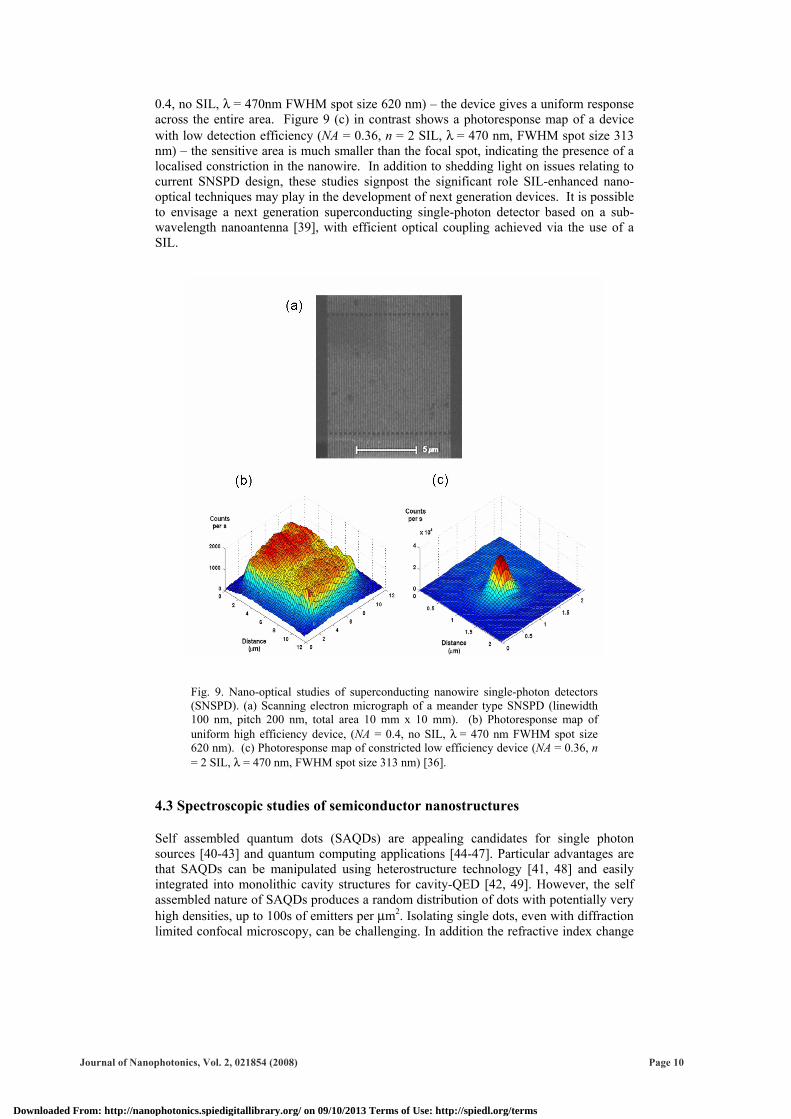
0.4, no SIL, λ = 470nm FWHM spot size 620 nm) – the device gives a uniform response across the entire area. Figure 9 (c) in contrast shows a photoresponse map of a device with low detection efficiency (NA = 0.36, n = 2 SIL, λ = 470 nm, FWHM spot size 313 nm) – the sensitive area is much smaller than the focal spot, indicating the presence of a localised constriction in the nanowire. In addition to shedding light on issues relating to current SNSPD design, these studies signpost the significant role SIL-enhanced nano-optical techniques may play in the development of next generation devices. It is possible to envisage a next generation superconducting single-photon detector based on a sub-wavelength nanoantenna [39], with efficient optical coupling achieved via the use of a SIL.
Fig. 9. Nano-optical studies of superconducting nanowire single-photon detectors (SNSPD). (a) Scanning electron micrograph of a meander type SNSPD (linewidth 100 nm, pitch 200 nm, total area 10 mm x 10 mm). (b) Photoresponse map of uniform high efficiency device, (NA = 0.4, no SIL, λ = 470 nm FWHM spot size 620 nm). (c) Photoresponse map of constricted low efficiency device (NA = 0.36, n = 2 SIL, λ = 470 nm, FWHM spot size 313 nm) [36].
4.3 Spectroscopic studies of semiconductor nanostructures Self assembled quantum dots (SAQDs) are appealing candidates for single photon sources [40-43] and quantum computing applications [44-47]. Particular advantages are that SAQDs can be manipulated using heterostructure technology [41, 48] and easily integrated into monolithic cavity structures for cavity-QED [42, 49]. However, the self assembled nature of SAQDs produces a random distribution of dots with potentially very high densities, up to 100s of emitters per µm2. Isolating single dots, even with diffraction limited confocal microscopy, can be challenging. In addition the refractive index change
Journal of Nanophotonics, Vol. 2, 021854 (2008) Page 10
Downloaded From: http://nanophotonics.spiedigitallibrary.org/ on 09/10/2013 Terms of Use: http://spiedl.org/terms
between the host material and the surrounding medium results in difficulties in efficiently collecting the emitted PL, which can limit device functionality.
Utilizing SIL technology has dual benefit for the optical study of single SAQDs. First, the improvement in spatial resolution decreases the spot size, thereby decreasing the number of dots under study. Second, SIL technology can reduce the refractive index change between the host material, GaAs (n = 3.5), and surrounding medium, normally helium gas or vacuum, leading to significant improvements to the PL extraction efficiency. A SAQD is essentially a point source which emits light equally in all directions. A single objective lens collects a cone of light emitted from that point source. The solid angle of such a cone is given by ( )θπ cos12 −=Ω where θ is the angle between the normal and the cone edge. The ratio of Ω to the solid angle of a sphere, 4π, gives the collection efficiency from the dot as: ( ) 2/cos1 θη −= . The 1/2 corresponds to the collection from only one cone of the point source emitter, due to the positioning of an objective lens on only one side of the sample. In terms of the effective numerical aperture of the system, NAeff, cos2θ = 1-NAeff
2. NAeff is given by NAobjnmat / ns where NAobj is the numerical aperture of the objective lens, ns is the refractive index of the host material and nmat the refractive index of the material directly above the host surface. This leads to a final collection efficiency of,
⎪⎭
⎪⎬
⎫
⎪⎩
⎪⎨
⎧
⎥⎥⎦
⎤
⎢⎢⎣
⎡⎟⎟⎠
⎞⎜⎜⎝
⎛−−=
21
2
1121
s
matobj
nnNA
η , (4)
Equation (4) shows that for a high-NA lens, for example 0.65 NA, typical collection efficiency from a single dot is 0.87%. The inclusion of a SIL alters nmat to nma t= nSIL for an h-SIL. For an s-SIL, nmat = nSIL
2, up to the limit where NAobj must be less than or equal to 1/nSIL. For example, a system with NAobj = 0.65 including a hemispherical SIL of n = 2.0 increases the collection efficiency of a single dot to 3.5% whilst simultaneously reducing the effective spot size by a factor of 4. In the ideal limit of an index matched s-SIL, theoretically the collection efficiency approaches 50%. While embedding a SAQD in a microcavity can increase collection efficiency through funnelling the PL into the cavity mode, effective tuning of the emission into cavity resonance is challenging and fabrication requirements limit the practical application of such an approach [42, 43, 49]. On the other hand, SIL technology provides a robust and practical solution to increased collection efficiencies with the added benefits of being compatible with other embedded point source emitters, for example NV centres in diamonds which are promising candidates for room temperature single photon sources[50].
Journal of Nanophotonics, Vol. 2, 021854 (2008) Page 11
Downloaded From: http://nanophotonics.spiedigitallibrary.org/ on 09/10/2013 Terms of Use: http://spiedl.org/terms
0
10
20
30
40
50
940 945 950 955 960
0
10
20
30
40
50C
ount
s pe
r Sec
ond
No SILAll Different Dots (All X1-)
With n = 2 hemispherical SIL
Wavelength (nm)
2X0
X1-
2X0h
All lines from same dot
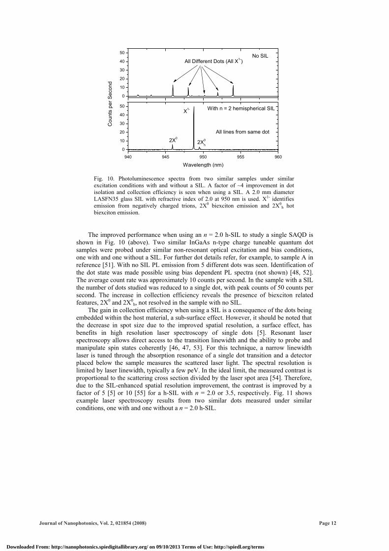
Fig. 10. Photoluminescence spectra from two similar samples under similar excitation conditions with and without a SIL. A factor of ~4 improvement in dot isolation and collection efficiency is seen when using a SIL. A 2.0 mm diameter LASFN35 glass SIL with refractive index of 2.0 at 950 nm is used. X1- identifies emission from negatively charged trions, 2X0 biexciton emission and 2X0
h hot biexciton emission.
The improved performance when using an n = 2.0 h-SIL to study a single SAQD is shown in Fig. 10 (above). Two similar InGaAs n-type charge tuneable quantum dot samples were probed under similar non-resonant optical excitation and bias conditions, one with and one without a SIL. For further dot details refer, for example, to sample A in reference [51]. With no SIL PL emission from 5 different dots was seen. Identification of the dot state was made possible using bias dependent PL spectra (not shown) [48, 52]. The average count rate was approximately 10 counts per second. In the sample with a SIL the number of dots studied was reduced to a single dot, with peak counts of 50 counts per second. The increase in collection efficiency reveals the presence of biexciton related features, 2X0 and 2X0
h, not resolved in the sample with no SIL. The gain in collection efficiency when using a SIL is a consequence of the dots being
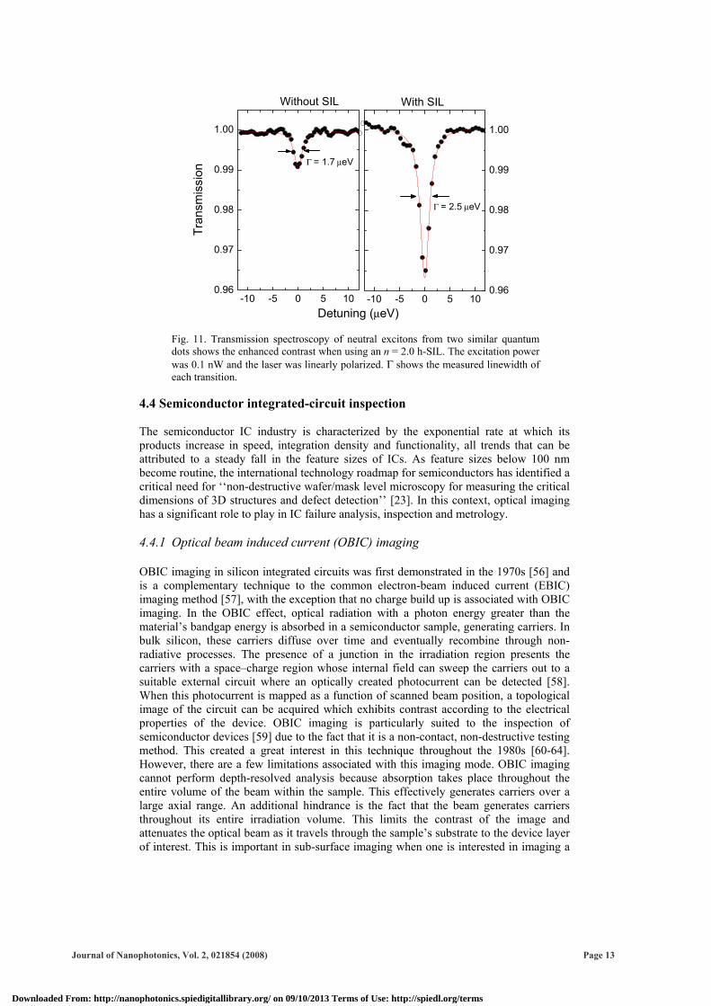
embedded within the host material, a sub-surface effect. However, it should be noted that the decrease in spot size due to the improved spatial resolution, a surface effect, has benefits in high resolution laser spectroscopy of single dots [5]. Resonant laser spectroscopy allows direct access to the transition linewidth and the ability to probe and manipulate spin states coherently [46, 47, 53]. For this technique, a narrow linewidth laser is tuned through the absorption resonance of a single dot transition and a detector placed below the sample measures the scattered laser light. The spectral resolution is limited by laser linewidth, typically a few peV. In the ideal limit, the measured contrast is proportional to the scattering cross section divided by the laser spot area [54]. Therefore, due to the SIL-enhanced spatial resolution improvement, the contrast is improved by a factor of 5 [5] or 10 [55] for a h-SIL with n = 2.0 or 3.5, respectively. Fig. 11 shows example laser spectroscopy results from two similar dots measured under similar conditions, one with and one without a n = 2.0 h-SIL.
Journal of Nanophotonics, Vol. 2, 021854 (2008) Page 12
Downloaded From: http://nanophotonics.spiedigitallibrary.org/ on 09/10/2013 Terms of Use: http://spiedl.org/terms
-10 -5 0 5 100.96
0.97
0.98
0.99
1.00
-10 -5 0 5 100.96
0.97
0.98
0.99
1.00
Γ = 1.7 µeV
Γ = 2.5 µeV Tr
ansm
issi
on
Without SIL
Detuning (µeV)
With SIL
Fig. 11. Transmission spectroscopy of neutral excitons from two similar quantum dots shows the enhanced contrast when using an n = 2.0 h-SIL. The excitation power was 0.1 nW and the laser was linearly polarized. Γ shows the measured linewidth of each transition.
4.4 Semiconductor integrated-circuit inspection
The semiconductor IC industry is characterized by the exponential rate at which its products increase in speed, integration density and functionality, all trends that can be attributed to a steady fall in the feature sizes of ICs. As feature sizes below 100 nm become routine, the international technology roadmap for semiconductors has identified a critical need for ‘‘non-destructive wafer/mask level microscopy for measuring the critical dimensions of 3D structures and defect detection’’ [23]. In this context, optical imaging has a significant role to play in IC failure analysis, inspection and metrology. 4.4.1 Optical beam induced current (OBIC) imaging OBIC imaging in silicon integrated circuits was first demonstrated in the 1970s [56] and is a complementary technique to the common electron-beam induced current (EBIC) imaging method [57], with the exception that no charge build up is associated with OBIC imaging. In the OBIC effect, optical radiation with a photon energy greater than the material’s bandgap energy is absorbed in a semiconductor sample, generating carriers. In bulk silicon, these carriers diffuse over time and eventually recombine through non-radiative processes. The presence of a junction in the irradiation region presents the carriers with a space–charge region whose internal field can sweep the carriers out to a suitable external circuit where an optically created photocurrent can be detected [58]. When this photocurrent is mapped as a function of scanned beam position, a topological image of the circuit can be acquired which exhibits contrast according to the electrical properties of the device. OBIC imaging is particularly suited to the inspection of semiconductor devices [59] due to the fact that it is a non-contact, non-destructive testing method. This created a great interest in this technique throughout the 1980s [60-64]. However, there are a few limitations associated with this imaging mode. OBIC imaging cannot perform depth-resolved analysis because absorption takes place throughout the entire volume of the beam within the sample. This effectively generates carriers over a large axial range. An additional hindrance is the fact that the beam generates carriers throughout its entire irradiation volume. This limits the contrast of the image and attenuates the optical beam as it travels through the sample’s substrate to the device layer of interest. This is important in sub-surface imaging when one is interested in imaging a
Journal of Nanophotonics, Vol. 2, 021854 (2008) Page 13
Downloaded From: http://nanophotonics.spiedigitallibrary.org/ on 09/10/2013 Terms of Use: http://spiedl.org/terms
structure that is buried several hundreds of microns below the surface of the sample. Modern flip-chip IC architectures highlight this issue since they are designed in a manner that does not allow front-side optical access to the circuit because of the numerous metallisation and interconnecting layers that occupy the top surface of the chip. For this reason, optical microscopy of flip-chips must be performed by backside imaging through the silicon substrate. This procedure presents the contradictory requirements of achieving high bulk transmission of the illuminating wavelength, yet also sufficient absorption at the same wavelength to generate carriers at the circuit features. These two requirements involve a delicate compromise between generated signal level, penetration depth, illumination wavelength and image contrast.
OBIC imaging is a linear technique and therefore suffers from the same limitations in resolution and contrast as laser fluorescence microscopy, including signal saturation and limited depth-resolution. For these reasons a nonlinear variant of the technique can be used, and the following section introduces the two-photon OBIC method which we have developed for three-dimensional imaging. 4.4.2 Two-photon optical beam induced current (TOBIC) microscopy Two-photon absorption is a nonlinear effect and, although it is difficult to measure using continuous-wave (CW) laser sources, it can be easily demonstrated with a few milliwatts of light using femtosecond pulses from a modelocked laser. TOBIC imaging was first demonstrated by Xu [65, 66] using a 1.3 µm femtosecond optical parametric oscillator, and addressed the contradictory requirements encountered using linear techniques of focusing through thick substrates while maintaining sufficient absorption at the beam focus of a laser beam to produce a strong OBIC signal. TOBIC imaging also has the attraction of producing an intrinsic increase in resolution for any given illuminating wavelength due to the nonlinear nature of the excitation. Two-photon absorption depends on the square of the optical intensity that arrives at the focus of the beam and therefore produces a reduction in the effective spot radius by a factor of 2 , assuming an incident Gaussian transverse profile. 4.4.3 Solid immersion lens microscopy using TOBIC imaging Ippolito et al. originally demonstrated that a SIL could be used to image a silicon chip and achieve a resolution of 230 nm under 1064 nm illumination in a confocal microscope [1]. Subsequently, we have demonstrated, using imaging at 1530 nm, optical resolutions approaching ~100 nm [3] by implementing TOBIC microscopy using an s-SIL. We used the s-SIL modality because we are interested in resolving circuit features located around 100 µm below the backside surface of the silicon die. The details of the prescription used to design the correct s-SIL for imaging at a given sub-surface depth have already been discussed. In a further analogy with two-photon fluorescence microscopy, we have also shown that the TOBIC effect can provide a means of generating ultra-high 2D and, in addition, 3D resolved imaging because the generation of significant photocurrent only occurs within one confocal parameter of the focused spot [2, 21, 67, 68]. The results are illustrated in Figures 12-14 below. The axial resolution provided is similar to that obtained through confocal imaging methods in which the double-pass of the imaging system improves its axial resolution [69]. The results shown here were an improvement on earlier performance obtained using a similar system [17]. This was attributed to a new ability to perform systematic axial scanning and thus an ability to localise the focus of the beam in the component layer of the chip more accurately.
Journal of Nanophotonics, Vol. 2, 021854 (2008) Page 14
Downloaded From: http://nanophotonics.spiedigitallibrary.org/ on 09/10/2013 Terms of Use: http://spiedl.org/terms
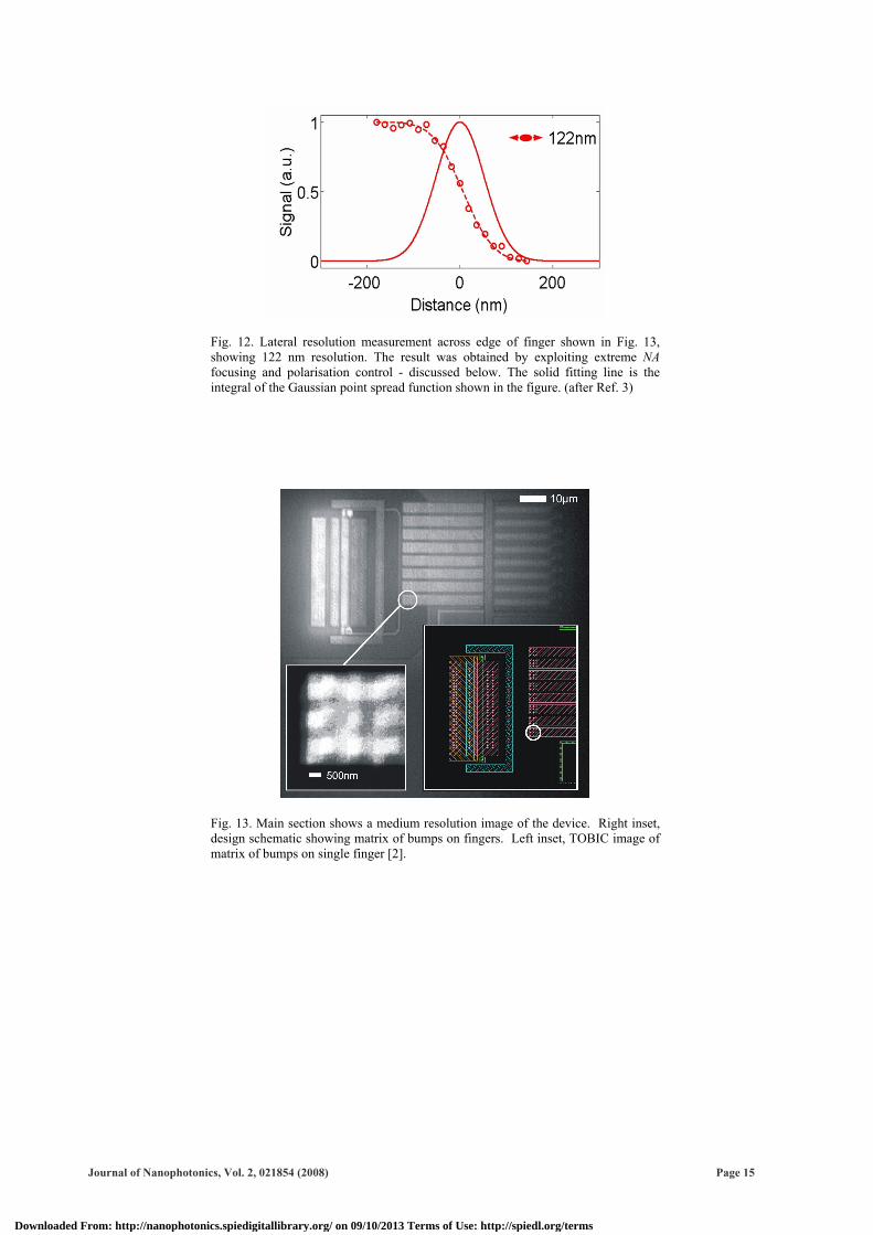
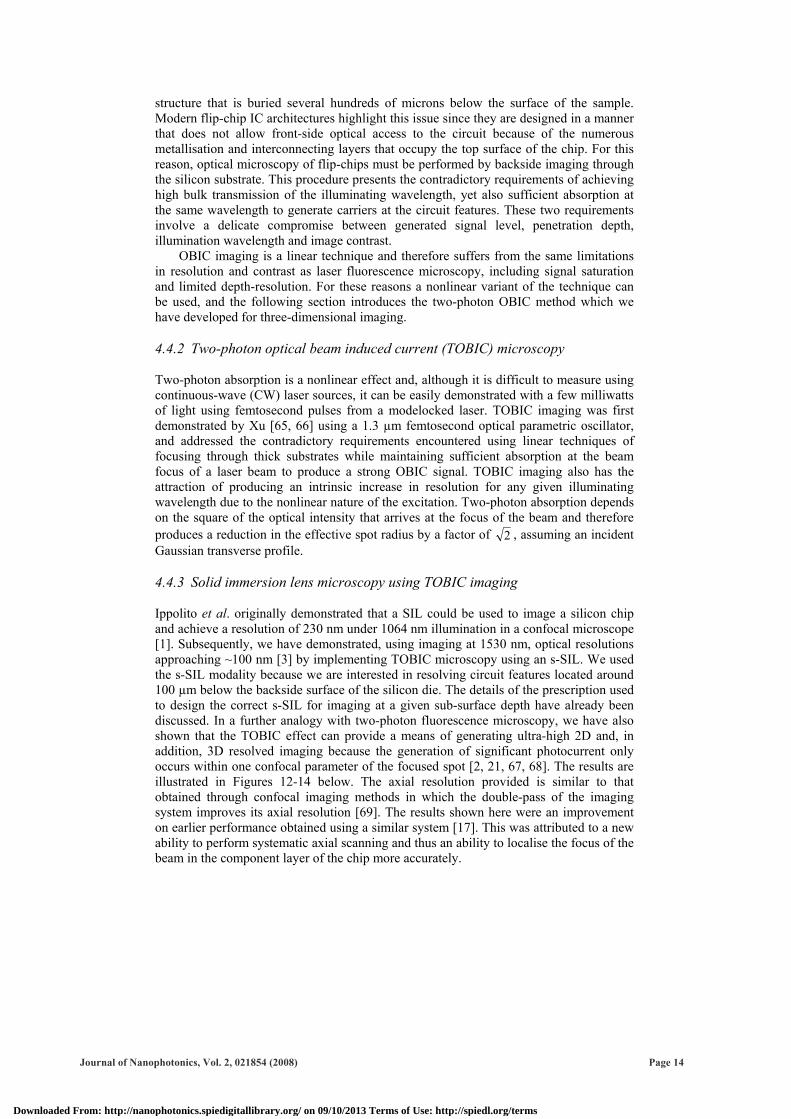
Fig. 12. Lateral resolution measurement across edge of finger shown in Fig. 13, showing 122 nm resolution. The result was obtained by exploiting extreme NA focusing and polarisation control - discussed below. The solid fitting line is the integral of the Gaussian point spread function shown in the figure. (after Ref. 3)
Fig. 13. Main section shows a medium resolution image of the device. Right inset, design schematic showing matrix of bumps on fingers. Left inset, TOBIC image of matrix of bumps on single finger [2].
Journal of Nanophotonics, Vol. 2, 021854 (2008) Page 15
Downloaded From: http://nanophotonics.spiedigitallibrary.org/ on 09/10/2013 Terms of Use: http://spiedl.org/terms
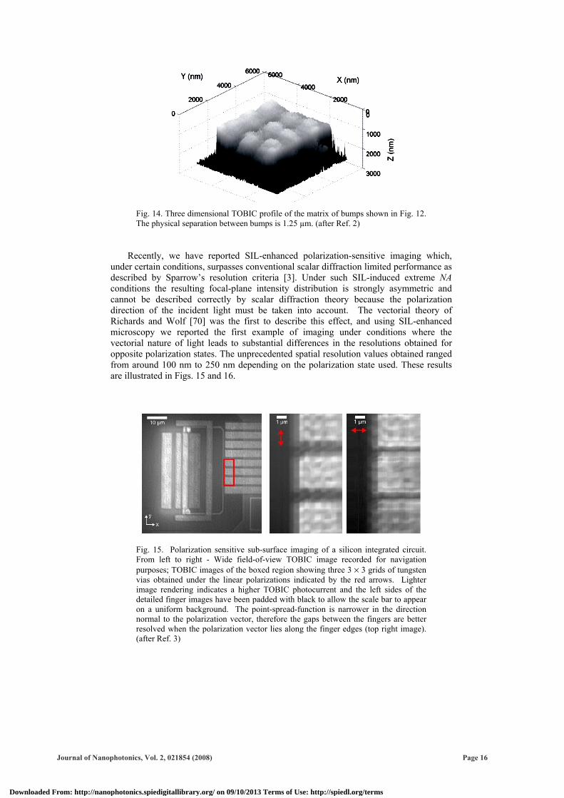
Fig. 14. Three dimensional TOBIC profile of the matrix of bumps shown in Fig. 12. The physical separation between bumps is 1.25 µm. (after Ref. 2)
Recently, we have reported SIL-enhanced polarization-sensitive imaging which, under certain conditions, surpasses conventional scalar diffraction limited performance as described by Sparrow’s resolution criteria [3]. Under such SIL-induced extreme NA conditions the resulting focal-plane intensity distribution is strongly asymmetric and cannot be described correctly by scalar diffraction theory because the polarization direction of the incident light must be taken into account. The vectorial theory of Richards and Wolf [70] was the first to describe this effect, and using SIL-enhanced microscopy we reported the first example of imaging under conditions where the vectorial nature of light leads to substantial differences in the resolutions obtained for opposite polarization states. The unprecedented spatial resolution values obtained ranged from around 100 nm to 250 nm depending on the polarization state used. These results are illustrated in Figs. 15 and 16.
Fig. 15. Polarization sensitive sub-surface imaging of a silicon integrated circuit. From left to right - Wide field-of-view TOBIC image recorded for navigation purposes; TOBIC images of the boxed region showing three 3 × 3 grids of tungsten vias obtained under the linear polarizations indicated by the red arrows. Lighter image rendering indicates a higher TOBIC photocurrent and the left sides of the detailed finger images have been padded with black to allow the scale bar to appear on a uniform background. The point-spread-function is narrower in the direction normal to the polarization vector, therefore the gaps between the fingers are better resolved when the polarization vector lies along the finger edges (top right image). (after Ref. 3)
Journal of Nanophotonics, Vol. 2, 021854 (2008) Page 16
Downloaded From: http://nanophotonics.spiedigitallibrary.org/ on 09/10/2013 Terms of Use: http://spiedl.org/terms
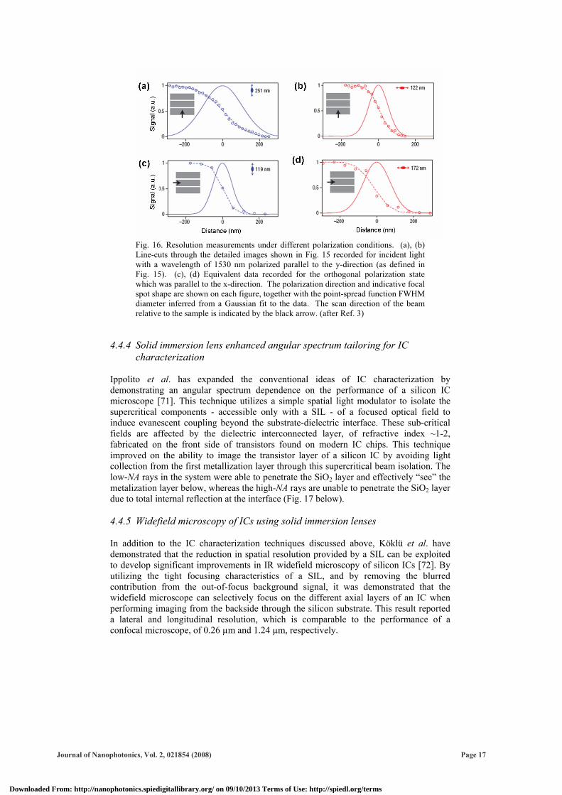
Fig. 16. Resolution measurements under different polarization conditions. (a), (b) Line-cuts through the detailed images shown in Fig. 15 recorded for incident light with a wavelength of 1530 nm polarized parallel to the y-direction (as defined in Fig. 15). (c), (d) Equivalent data recorded for the orthogonal polarization state which was parallel to the x-direction. The polarization direction and indicative focal spot shape are shown on each figure, together with the point-spread function FWHM diameter inferred from a Gaussian fit to the data. The scan direction of the beam relative to the sample is indicated by the black arrow. (after Ref. 3)
4.4.4 Solid immersion lens enhanced angular spectrum tailoring for IC
characterization Ippolito et al. has expanded the conventional ideas of IC characterization by demonstrating an angular spectrum dependence on the performance of a silicon IC microscope [71]. This technique utilizes a simple spatial light modulator to isolate the supercritical components - accessible only with a SIL - of a focused optical field to induce evanescent coupling beyond the substrate-dielectric interface. These sub-critical fields are affected by the dielectric interconnected layer, of refractive index ~1-2, fabricated on the front side of transistors found on modern IC chips. This technique improved on the ability to image the transistor layer of a silicon IC by avoiding light collection from the first metallization layer through this supercritical beam isolation. The low-NA rays in the system were able to penetrate the SiO2 layer and effectively “see” the metalization layer below, whereas the high-NA rays are unable to penetrate the SiO2 layer due to total internal reflection at the interface (Fig. 17 below). 4.4.5 Widefield microscopy of ICs using solid immersion lenses In addition to the IC characterization techniques discussed above, Köklü et al. have demonstrated that the reduction in spatial resolution provided by a SIL can be exploited to develop significant improvements in IR widefield microscopy of silicon ICs [72]. By utilizing the tight focusing characteristics of a SIL, and by removing the blurred contribution from the out-of-focus background signal, it was demonstrated that the widefield microscope can selectively focus on the different axial layers of an IC when performing imaging from the backside through the silicon substrate. This result reported a lateral and longitudinal resolution, which is comparable to the performance of a confocal microscope, of 0.26 µm and 1.24 µm, respectively.
Journal of Nanophotonics, Vol. 2, 021854 (2008) Page 17
Downloaded From: http://nanophotonics.spiedigitallibrary.org/ on 09/10/2013 Terms of Use: http://spiedl.org/terms
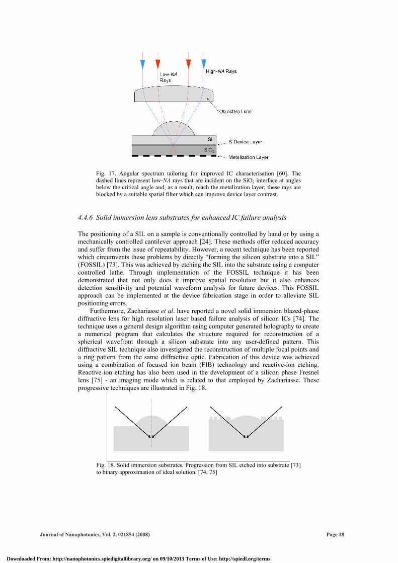
Fig. 17. Angular spectrum tailoring for improved IC characterisation [60]. The dashed lines represent low-NA rays that are incident on the SiO2 interface at angles below the critical angle and, as a result, reach the metalization layer; these rays are blocked by a suitable spatial filter which can improve device layer contrast.
4.4.6 Solid immersion lens substrates for enhanced IC failure analysis The positioning of a SIL on a sample is conventionally controlled by hand or by using a mechanically controlled cantilever approach [24]. These methods offer reduced accuracy and suffer from the issue of repeatability. However, a recent technique has been reported which circumvents these problems by directly “forming the silicon substrate into a SIL” (FOSSIL) [73]. This was achieved by etching the SIL into the substrate using a computer controlled lathe. Through implementation of the FOSSIL technique it has been demonstrated that not only does it improve spatial resolution but it also enhances detection sensitivity and potential waveform analysis for future devices. This FOSSIL approach can be implemented at the device fabrication stage in order to alleviate SIL positioning errors.
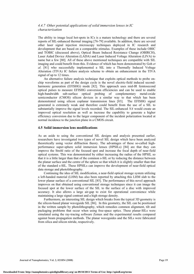
Furthermore, Zachariasse et al. have reported a novel solid immersion blazed-phase diffractive lens for high resolution laser based failure analysis of silicon ICs [74]. The technique uses a general design algorithm using computer generated holography to create a numerical program that calculates the structure required for reconstruction of a spherical wavefront through a silicon substrate into any user-defined pattern. This diffractive SIL technique also investigated the reconstruction of multiple focal points and a ring pattern from the same diffractive optic. Fabrication of this device was achieved using a combination of focused ion beam (FIB) technology and reactive-ion etching. Reactive-ion etching has also been used in the development of a silicon phase Fresnel lens [75] - an imaging mode which is related to that employed by Zachariasse. These progressive techniques are illustrated in Fig. 18.
Fig. 18. Solid immersion substrates. Progression from SIL etched into substrate [73] to binary approximation of ideal solution. [74, 75]
Journal of Nanophotonics, Vol. 2, 021854 (2008) Page 18
Downloaded From: http://nanophotonics.spiedigitallibrary.org/ on 09/10/2013 Terms of Use: http://spiedl.org/terms
4.4.7 Other potential applications of solid immersion lenses in IC characterization The ability to image local hot-spots in ICs is a mature technology and there are several reports of SIL-enhanced thermal imaging [76-79] available. In addition, there are several other laser signal injection microscopy techniques deployed in IC research and development that are based on a comparable stimulus. Examples of these include OBIC and TOBIC (discussed above), Optical Beam Induced Resistance Change (OBIRCH), Laser Aided Device Alteration (LADA) and Laser Induced Voltage Alteration (LIVA) to name but a few [80]. All of these above mentioned techniques are compatible with SIL imaging and could benefit from this. Evidence of which has been demonstrated by Goh et al. [81] who successfully implemented a SIL into a Thermally Induced Voltage Alteration (TIVA) IC failure analysis scheme to obtain an enhancement in the TIVA signal of up to 12 times.
An alternative failure analysis technique that exploits optical methods to probe on-chip waveforms as part of the design cycle is the novel electric-field induced second-harmonic generation (EFISHG) mode [82]. This approach uses mid-IR femtosecond optical pulses to measure EFISHG conversion efficiencies and can be used to enable high-bandwidth sub-surface optical probing of complementary metal-oxide semiconductor (CMOS) silicon devices in a similar way to that which has been demonstrated using silicon coplanar transmission lines [83]. The EFISHG signal generated is extremely weak and therefore could benefit from the use of a SIL to substantially improve the signal levels recorded. The SIL-enhanced NA would create an improved optical resolution as well as increase the capability to generate a higher efficiency conversion due to the larger component of the incident polarization located at normal incidence to the junction plane in a CMOS circuit. 4.5 Solid immersion lens modifications As an aside to using the conventional SIL designs and analysis presented earlier, researchers have investigated two types of novel SIL design which have been analyzed theoretically using vector diffraction theory. The advantages of these so-called high-performance super-sphere solid immersion lenses (HPSILs) [84] are that they can improve the Strehl ratio of the focused spot and increase the focal depth of near-field optical systems. This was demonstrated by either increasing the radius of the HPSIL so that it is a little larger than that of the common s-SIL or by reducing the distance between the planar surface and the centre of the sphere so that which it is slightly smaller than that of the standard s-SIL. These HPSILs can improve the development of near-field optical data storage and photolithography.
Continuing the idea of SIL modification, a near-field optical storage system utilizing a left-handed material (LHM) has also been reported by attaching this LHM slab to the lower planar surface of a conventional SIL [85]. The performance of this novel approach improves on that obtained using conventional storage techniques since it can image the focused spot at the lower surface of the SIL to the surface of a disc with improved accuracy. It also allows a large air-gap to exist for operational convenience while maintaining a large signal contrast and a high storage density.
Furthermore, an interesting SIL design which breaks from the typical 3D geometry is the silicon-based planar waveguide SIL [86]. In this geometry, the SIL can be positioned in the written sample by photolithography, which remedies common alignment, tilt and packaging problems that occur when using free-space optics. These planar-SILs were simulated using the ray-tracing software Zemax and the experimental results compared against beam propagation methods. The planar waveguides and the SILs were fabricated from silica and silicon nitride, respectively.
Journal of Nanophotonics, Vol. 2, 021854 (2008) Page 19
Downloaded From: http://nanophotonics.spiedigitallibrary.org/ on 09/10/2013 Terms of Use: http://spiedl.org/terms
4.6 Microfabricated solid immersion lens Fletcher and Crozier et al. have presented both a microfabricated silicon and silicon nitride SIL for deployment in scanning microscopy applications [87, 88]. Both SILs were fabricated onto individual cantilevers for scanning, and a tip was fabricated opposite the SIL to localise SIL-sample contact. The results from this approach demonstrate sub-diffraction limited performance in both cases. This technique shares common aspects with that demonstrated by Lerman et al. who applied SIL near-field optics to Raman analysis of strained silicon thin films [89]. However, instead of the SIL fabrication taking place on a cantilever, the SIL was positioned on the end of an optical fibre. These scanning microscopy methods that utilize atomic force microscopy (AFM) style cantilevers provide an important tool on the investigation of microelectronic devices. 5 CONCLUSIONS AND FUTURE DEVELOPMENTS The combination of SIL imaging with pupil-function engineering offers a potential route to achieving optical super-resolution with unprecedented performance. In the context of imaging, super-resolution refers to any technique that improves the resolution of an imaging system beyond the conventional diffraction-limited value [90]. Such techniques can be attractive because they often provide a simple way to enhance the resolution of an optical system without resorting to more sophisticated near-field methods. An additional embodiment of optical super-resolution is the use of pupil-function engineering to manipulate the point spread function (PSF) at the focal plane of an imaging system, since the PSF has a radial profile whose shape depends sensitively on the aperture function of the system [91-93]. The PSF is defined as the irradiance distribution at the focal plane of an imaging system which is produced when imaging a point source [90]. Control of the PSF using pupil-function engineering has been applied in optical data storage [94] to increase the storage density on a disc by manipulating the radial profile of the read beam. In this example, a further advantage is obtained because reducing the width of the radial PSF can lead to a corresponding extension of the axial PSF, relaxing the requirement to maintain the read lens at a precise distance from the disc [95].
A second approach in the pursuit of optical super-resolution is to exploit extreme NA focusing, a SIL-induced condition, using linear polarized light. The spatial distribution of an optical field at the focus of a high-NA lens displays an increasing ellipticity as the NA of the system approaches unity. This is because at high-NA polarization starts to play a more dominant role in the focal properties of the incident light. In the effort to obtain the smallest possible focal spot size one must take this into account since polarization-sensitive effects are no longer negligible.
The original theoretical vector diffraction analysis of high-NA focusing was published by Richards and Wolf [70] which investigates the structure of a linearly polarized electromagnetic field near the focus of a high-NA aplanatic lens system which images a point source at infinity. Richards and Wolf adopt an analytical integral representation of the electromagnetic field whereas others have implemented a different methodology to calculate the field near the focus of a high-NA objective lens. Instead of applying direct integration, Leutenegger et al. [96] evaluates the vectorial Debye diffraction integral with a fast Fourier transform (FFT) to calculate the electromagnetic field in the entire focal region. This technique enhances the speed at which these calculations can take place since it employs a sampling grid procedure in combination with the FFT analysis.
Fig. 20 illustrates the effects of increasing NA on the physical dimensions of the resulting PSF in the focal plane both with and without an annular aperture of 90% obscuration. These 2D plots were generated using the method described by Leutenegger in [96]. The PSFs were calculated using NA values corresponding to angular semi-apertures in the object space of 1.0sin =θ and 95.0sin =θ .
Journal of Nanophotonics, Vol. 2, 021854 (2008) Page 20
Downloaded From: http://nanophotonics.spiedigitallibrary.org/ on 09/10/2013 Terms of Use: http://spiedl.org/terms
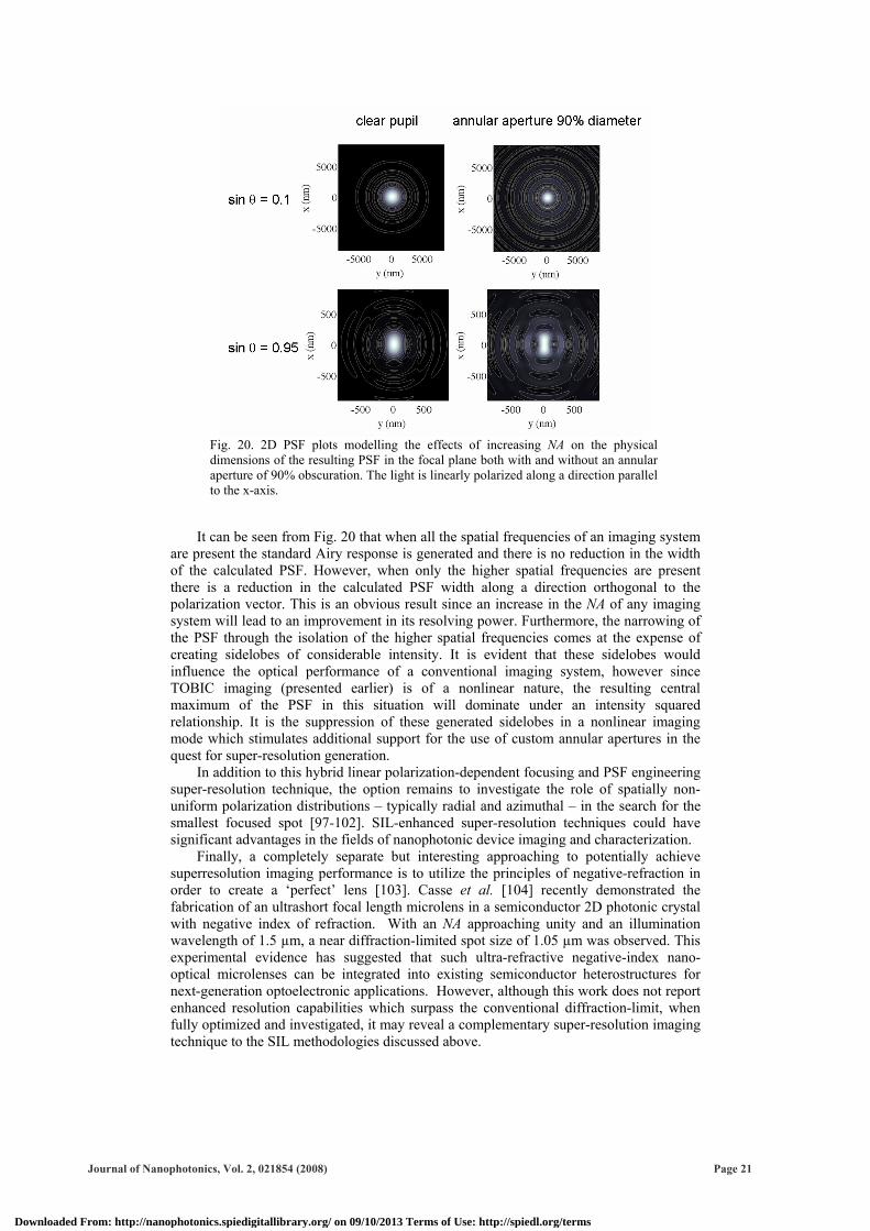
Fig. 20. 2D PSF plots modelling the effects of increasing NA on the physical dimensions of the resulting PSF in the focal plane both with and without an annular aperture of 90% obscuration. The light is linearly polarized along a direction parallel to the x-axis.
It can be seen from Fig. 20 that when all the spatial frequencies of an imaging system are present the standard Airy response is generated and there is no reduction in the width of the calculated PSF. However, when only the higher spatial frequencies are present there is a reduction in the calculated PSF width along a direction orthogonal to the polarization vector. This is an obvious result since an increase in the NA of any imaging system will lead to an improvement in its resolving power. Furthermore, the narrowing of the PSF through the isolation of the higher spatial frequencies comes at the expense of creating sidelobes of considerable intensity. It is evident that these sidelobes would influence the optical performance of a conventional imaging system, however since TOBIC imaging (presented earlier) is of a nonlinear nature, the resulting central maximum of the PSF in this situation will dominate under an intensity squared relationship. It is the suppression of these generated sidelobes in a nonlinear imaging mode which stimulates additional support for the use of custom annular apertures in the quest for super-resolution generation.
In addition to this hybrid linear polarization-dependent focusing and PSF engineering super-resolution technique, the option remains to investigate the role of spatially non-uniform polarization distributions – typically radial and azimuthal – in the search for the smallest focused spot [97-102]. SIL-enhanced super-resolution techniques could have significant advantages in the fields of nanophotonic device imaging and characterization.
Finally, a completely separate but interesting approaching to potentially achieve superresolution imaging performance is to utilize the principles of negative-refraction in order to create a ‘perfect’ lens [103]. Casse et al. [104] recently demonstrated the fabrication of an ultrashort focal length microlens in a semiconductor 2D photonic crystal with negative index of refraction. With an NA approaching unity and an illumination wavelength of 1.5 µm, a near diffraction-limited spot size of 1.05 µm was observed. This experimental evidence has suggested that such ultra-refractive negative-index nano-optical microlenses can be integrated into existing semiconductor heterostructures for next-generation optoelectronic applications. However, although this work does not report enhanced resolution capabilities which surpass the conventional diffraction-limit, when fully optimized and investigated, it may reveal a complementary super-resolution imaging technique to the SIL methodologies discussed above.
Journal of Nanophotonics, Vol. 2, 021854 (2008) Page 21
Downloaded From: http://nanophotonics.spiedigitallibrary.org/ on 09/10/2013 Terms of Use: http://spiedl.org/terms
In conclusion, the solid immersion lens has contributed to the advance of high-resolution imaging and probing in several areas of physics and photonics. This simple but powerful optical component has facilitated a substantial volume of high-resolution data that has supported detailed theoretical and experimental analysis. Although this paper has maintained an optoelectronic device characterization bias, the solid immersion lens can, and has, played a significant role in the advance of several other areas of science and technology, including biophotonics and microfabrication. Acknowledgments The Ultrafast Optics Group acknowledge the financial support of the UK Engineering and Physical Sciences Research Council (EPRSC) under project code EP/C509765/1 and Credence Systems Corp, CA, USA, for supplying the device under investigation. RHH is supported by the Royal Society of London (via a University Research Fellowship) and EPSRC EP/F009968/1. RHH acknowledges assistance from colleagues at NIST, USA and thanks G. Golt’sman of Moscow State Pedagogical University for supplying the SNSPD devices used in the nano-optical studies. References
[1] S. B. Ippolito, B. B. Goldberg, and M. S. Unlu, "High spatial resolution subsurface microscopy," Appl. Phys. Lett. 78, 4071-4073 (2001) [doi:10.1063/1.1381574].
[2] E. Ramsay, K. A. Serrels, M. J. Thomson, A. J. Waddie, M. R. Taghizadeh, R. J. Warburton, and D. T. Reid, "Three-dimensional nanoscale subsurface optical imaging of silicon circuits," Appl. Phys. Lett. 90, 131101 (2007) [doi:10.1063/1.2716344].
[3] K. A. Serrels, E. Ramsay, R. J. Warburton, and D. T. Reid, "Nanoscale optical microscopy in the vectorial focusing regime," Nature Photon. 2, 311-314 (2008) [doi:10.1038/nphoton.2008.29].
[4] P. A. Dalgarno, J. McFarlane, D. Brunner, R. W. Lambert, B. D. Gerardot, R. J. Warburton, K. Karrai, A. Badolato, and P. M. Petroff, "Hole recapture limited single photon generation from a single n-type charge-tunable quantum dot," Appl. Phys. Lett. 92, 193103-193103 (2008) [doi:10.1063/1.2924315].
[5] B. D. Gerardot, S. Seidl, P. A. Dalgarno, R. J. Warburton, M. Kroner, K. Karrai, A. Badolato, and P. M. Petroff, "Contrast in transmission spectroscopy of a single quantum dot," Appl. Phys. Lett. 90, 221106 (2007) [doi:10.1063/1.2743750].
[6] I. Ichimura, S. Hayashi, and G.S. Kino, "High-density optical recording using a solid immersion lens," Appl. Opt. 36, 4339-4348 (1997) [doi:10.1364/AO.36.004339].
[7] B. D. Terris, H. J. Mamin, and D. Rugar, "Optical-data storage using a solid immersion lens," Optoelectron. Devices Technol. 10, 303-310 (1995).
[8] L. P. Ghislain, V. B. Elings, K. B. Crozier, S. R. Manalis, S. C. Minne, K. Wilder, G. S. Kino, and C. F. Quate, "Near-field photolithography with a solid immersion lens," Appl. Phys. Lett. 74, 501-503 (1999) [doi:10.1063/1.123168].
[9] C. M. Sparrow, "On spectroscopic resolving power," Astrophys. J. 44, 76 (1916) [doi:10.1086/142271].
[10] M. Born and E. Wolf, Principles of Optics, 7th ed., Cambridge University Press, Cambridge (2002).
[11] G. S. Kino and S. M. Mansfield, Near field and solid immersion optical microscope - US Patent Number 5,004,307. 1991: United States of America.
[12] S. M. Mansfield and G. S. Kino, "Solid immersion microscope," Appl. Phys. Lett. 57, 2615-2616 (1990) [doi:10.1063/1.103828].
Journal of Nanophotonics, Vol. 2, 021854 (2008) Page 22
Downloaded From: http://nanophotonics.spiedigitallibrary.org/ on 09/10/2013 Terms of Use: http://spiedl.org/terms
[13] K. R. Spring, M. J. Parry-Hill, and M. W. Davidson, Molecular Expressions Microscopy Primer: Anatomy of the Microscope - Oil Immersion: Interactive Java Tutorial, (2004).
[14] B. B. Goldberg, S. B. Ippolito, L. Novotny, Z. Liu, and M.S . Unlu, "Immersion lens microscopy of photonic nanostructures and quantum dots," IEEE J. Sel. Top. Quantum Electron. 8, 1051-1059 (2002) [doi:10.1109/JSTQE.2002.804232].
[15] A. N. Vamivakas, R. D. Younger, B. B. Goldberg, A. K. Swan, M. S. Unlu, E. R. Behringer, and S. B. Ippolito, "A case study for optics: the solid immersion microscope," Am. J. Phys. 76, 758-768 (2008) [doi:10.1119/1.2908186].
[16] Z. H. Liu, B. B. Goldberg, S. B. Ippolito, A. N. Vamivakas, M. S. Unlu, and R. Mirin, "High resolution, high collection efficiency in numerical aperture increasing lens microscopy of individual quantum dots," Appl. Phys. Lett. 87, 071905 (2005) [doi:10.1063/1.2012532].
[17] E. Ramsay, N. Pleynet, D. Xiao, R. J. Warburton, and D. T. Reid, "Two-photon optical-beam-induced current solid-immersion imaging of a silicon flip chip with a resolution of 325 nm," Opt. Lett. 30, 26-28 (2005) [doi:10.1364/OL.30.000026].
[18] M. Baba, T. Sasaki, M. Yoshita, and H. Akiyama, "Aberrations and allowances for errors in a hemisphere solid immersion lens for submicron-resolution photoluminescence microscopy," J. Appl. Phys. 85, 6923-6925 (1999) [doi:10.1063/1.370107].
[19] K. Karrai, X. Lorenz, and L. Novotny, "Enhanced reflectivity contrast in confocal solid immersion lens microscopy," Appl. Phys. Lett. 77, 3459-3461 (2000) [doi:10.1063/1.1326839].
[20] Q. Wu, R. D. Grober, D. Gammon, and D. S. Katzer, "Imaging spectroscopy of two-dimensional excitons in a narrow GaAs/AlGaAs quantum well," Phys. Rev. Lett. 83, 2652-2655 (1999) [doi:10.1103/PhysRevLett.83.2652].
[21] E. Ramsay, K. A. Serrels, M. J. Thomson, A. J. Waddle, R. J. Warburton, M. R. Taghizadeh, and D. T. Reid, "Three-dimensional nanometric sub-surface imaging of a silicon flip-chip using the two-photon optical beam induced current method," Microelectron. Reliability 47, 1534-1538 (2007) [doi:10.1016/j.microrel.2007.07.069].
[22] S. B. Ippolito, B. B. Goldberg, and M. S. Unlu, "Theoretical analysis of numerical aperture increasing lens microscopy," J. Appl. Phys. 97, 053105 (2005) [doi:10.1063/1.1858060].
[23] International Technology Roadmap for Semiconductors - Executive Summary, (2003).
[24] B. D. Terris, H. J. Mamin, D. Rugar, W. R. Studenmund, and G. S. Kino, "Near-field optical-data storage using a solid immersion lens," Appl. Phys. Lett. 65, 388-390 (1994) [doi:10.1063/1.112341].
[25] M. Shinoda, K. Saito, T. Kondo, A. Nakaoki, M. Furuki, M. Takeda, M. Yamamoto, T. J. Schaich, B. M. Van Oerle, H. P. Godfried, P. A. C. Kriele, E. P. Houwman, W. H. M. Nelissen, G. J. Pels, and P. G. M. Spaaij, "High-density near-field readout using diamond solid immersion lens," Japan. J. Appl. Phys. Part 1. 45, 1311-1313 (2006) [doi:10.1143/JJAP.45.1311].
[26] S. M. Mansfield, W. R. Studenmund, G. S. Kino, and K. Osato, "High-numerical-aperture lens system for optical storage," Opt. Lett. 18, 305-307 (1993) [doi:10.1364/OL.18.000305].
[27] Y. J. Zhang, "Optical intensity distribution of a plano-convex solid immersion mirror," J. Opt. Soc. Am. A. 24, 211-214 (2007) [doi:10.1364/JOSAA.24.000211]
[28] C. B. Peng, C. Mihalcea, D. Buchel, W. A. Challener, and E. C. Gage, "Near-field optical recording using a planar solid immersion mirror," Appl. Phys. Lett. 87, 151105(2005) [doi:10.1063/1.2093937].
Journal of Nanophotonics, Vol. 2, 021854 (2008) Page 23
Downloaded From: http://nanophotonics.spiedigitallibrary.org/ on 09/10/2013 Terms of Use: http://spiedl.org/terms
[29] W. A. Challener, C. Mihalcea, C. B. Peng, and K. Pelhos, "Miniature planar solid immersion mirror with focused spot less than a quarter wavelength," Opt. Exp. 13, 7189-7197 (2005) [doi:10.1364/OPEX.13.007189].
[30] Y. J. Zhang, "Optical data storage system with a planoellipsoidal solid immersion mirror illuminated directly by a point light source," Appl. Opt. 45, 8653-8658 (2006) [doi:10.1364/AO.45.008653].
[31] A. Migdall and J. Dowling, "Introduction to Journal of Modern Optics Special Issue on single-photon detectors, applications, and measurement methods," J. Mod. Opt. 51, 1265-1266 (2004) [doi:10.1080/09500340408235271].
[32] G. N. Gol'tsman, O. Okunev, G. Chulkova, A. Lipatov, A. Semenov, K. Smirnov, B. Voronov, A. Dzardanov, C. Williams, and R. Sobolewski, "Picosecond superconducting single-photon optical detector," Appl. Phys. Lett. 79, 705-707 (2001)[doi:10.1063/1.1388868].
[33] J. Chen, J. B. Altepeter, M. Medic, K. F. Lee, B. Gokden, R. H. Hadfield, S. W. Nam, and P. Kumar, "Demonstration of a quantum controlled-NOT gate in the telecommunications band," Phys. Rev. Lett. 100, 133603 (2008) [doi:10.1103/PhysRevLett.100.133603].
[34] R. H. Hadfield, M. J. Stevens, S. S. Gruber, A. J. Miller, R. E. Schwall, R. P. Mirin, and S. W. Nam, "Single photon source characterization with a superconducting single photon detector," Opt. Exp. 13, 10846-10853 (2005) [doi:10.1364/OPEX.13.010846].
[35] H. Takesue, S. W. Nam, Q. Zhang, R. H. Hadfield, T. Honjo, K. Tamaki, and Y. Yamamoto, "Quantum key distribution over a 40-dB channel loss using superconducting single-photon detectors," Nature Photon. 1, 343-348 (2007) [doi:10.1038/nphoton.2007.75].
[36] A. Verevkin, J. Zhang, R. Sobolewski, A. Lipatov, O. Okunev, G. Chulkova, A. Korneev, K. Smirnov, G.N. Gol'tsman, and A. Semenov, "Detection efficiency of large-active-area NbN single-photon superconducting detectors in the ultraviolet to near-infrared range," Appl. Phys. Lett. 80, 4687-4689 (2002) [doi:10.1063/1.1487924].
[37] A. J. Kerman, E. A. Dauler, J. K. W. Yang, K. M. Rosfjord, V. Anant, K. K. Berggren, G. N. Gol'tsman, and B. M. Voronov, "Constriction-limited detection efficiency of superconducting nanowire single-photon detectors," Appl. Phys. Lett. 90, 101110 (2007) [doi:10.1063/1.2696926].
[38] R. H. Hadfield, P. A. Dalgarno, J. A. O'Connor, E. Ramsay, R. J. Warburton, E. J. Gansen, B. Baek, M. J. Stevens, R. P. Mirin, and S. W. Nam, "Submicrometer photoresponse mapping of nanowire superconducting single-photon detectors," Appl. Phys. Lett. 91, 241108 (2007) [doi:10.1063/1.2824384].
[39] L. Tang, S. E. Kocabas, S. Latif, A. K. Okyay, D. S. Ly-Gagnon, K. C. Saraswat, and D. A. B. Miller, "Nanometre-scale germanium photodetector enhanced by a near-infrared dipole antenna," Nature Photon. 2, 226-229 (2008) [doi:10.1038/nphoton.2008.30].
[40] C. Santori, D. Fattal, J. Vuckovic, G. S. Solomon, and Y. Yamamoto, "Single-photon generation with InAs quantum dots," New J. Physics. 6, 89 (2004) [doi:10.1088/1367-2630/6/1/089].
[41] Z. L. Yuan, B. E. Kardynal, R. M. Stevenson, A. J. Shields, C. J. Lobo, K. Cooper, N. S. Beattie, D. A. Ritchie, and M. Pepper, "Electrically driven single-photon source," Science 295, 102-105 (2002) [doi:10.1126/science.1066790].
[42] S. Strauf, N. G. Stoltz, M. T. Rakher, L. A. Coldren, P. M. Petroff, and D. Bouwmeester, "High-frequency single-photon source with polarization control," Nature Photon. 1, 704-708 (2007) [doi:10.1038/nphoton.2007.227].
[43] P. Michler, A. Kiraz, C. Becher, W. V. Schoenfeld, P. M. Petroff, L. D. Zhang, E. Hu, and A. Imamoglu, "A quantum dot single-photon turnstile device," Science 290, 2282-2285 (2000) [doi: 10.1126/science.290.5500.2282].
Journal of Nanophotonics, Vol. 2, 021854 (2008) Page 24
Downloaded From: http://nanophotonics.spiedigitallibrary.org/ on 09/10/2013 Terms of Use: http://spiedl.org/terms
[44] D. P. DiVincenzo and D. Loss, "Quantum information is physical," Superlattice. Microst. 23, 419-432 (1998) [doi:10.1006/spmi.1997.0520]
[45] M. Kroutvar, Y. Ducommun, D. Heiss, M. Bichler, D. Schuh, G. Abstreiter, and J. J. Finley, "Optically programmable electron spin memory using semiconductor quantum dots," Nature 432, 81-84 (2004) [doi:10.1038/nature03008].
[46] B. D. Gerardot, D. Brunner, P. A. Dalgarno, P. Ohberg, S. Seidl, M. Kroner, K. Karrai, N. G. Stoltz, P. M. Petroff, and R. J. Warburton, "Optical pumping of a single hole spin in a quantum dot," Nature 451, 441-444 (2008) [doi:10.1038/nature06472].
[47] M. Atature, J. Dreiser, A. Badolato, A. Hogele, K. Karrai, and A. Imamoglu, "Quantum-dot spin-state preparation with near-unity fidelity," Science 312, 551-553 (2006) [doi:10.1126/science.1126074].
[48] R. J. Warburton, C. Schaflein, D. Haft, F. Bickel, A. Lorke, K. Karrai, J. M. Garcia, W. Schoenfeld, and P. M. Petroff, "Optical emission from a charge-tunable quantum ring," Nature 405, 926-929 (2000) [doi:10.1038/35016030] .
[49] A. Badolato, K. Hennessy, M. Atature, J. Dreiser, E. Hu, P. M. Petroff, and A. Imamoglu, "Deterministic coupling of single quantum dots to single nanocavity modes," Science 308, 1158-1161 (2005) [doi:10.1126/science.1109815].
[50] C. Kurtsiefer, S. Mayer, P. Zarda, and H. Weinfurter, "Stable solid-state source of single photons," Phys. Rev. Lett. 85, 290-293 (2000)[doi:10.1103/PhysRevLett.85.290].
[51] P. A. Dalgarno, J. McFarlane, D. Brunner, R. W. Lambert, B. D. Gerardot, R. J. Warburton, K. Karrai, A. Badolato, and P. M. Petroff, "Hole recapture limited single photon generation from a single n-type charge-tunable quantum dot," Appl. Phys. Lett. 92, 193103-3 (2008)[doi:10.1063/1.2924315].
[52] B. Urbaszek, R. J. Warburton, K. Karrai, B. D. Gerardot, P. M. Petroff, and J.M. Garcia, "Fine structure of highly charged excitons in semiconductor quantum dots," Phys. Rev. Lett. 90, 247403 (2003) [doi:10.1103/PhysRevLett.90.247403].
[53] A. Hogele, S. Seidl, M. Kroner, K. Karrai, R. J. Warburton, B. D. Gerardot, and P. M. Petroff, "Voltage-controlled optics of a quantum dot," Phys. Rev. Lett. 93, 217401 (2004) [doi:10.1103/PhysRevLett.93.217401].
[54] K. Karrai and R. J. Warburton, "Optical transmission and reflection spectroscopy of single quantum dots," Superlattice. Microst. 33, 311-337 (2003) [doi:10.1016/j.spmi.2004.02.007].
[55] A. N. Vamivakas, M. Atature, J. Dreiser, S. T. Yilmaz, A. Badolato, A. K. Swan, B. B. Goldberg, A. Imamoglu, and M. S. Unlu, "Strong extinction of a far-field laser beam by a single quantum dot," Nano Lett. 7, 2892-2896 (2007) [doi:10.1021/nl0717255].
[56] T. Wilson and J. N. Gannaway, "Examination of grain boundaries in polycrystalline solar cells using a scanning optical microscope," Electron. Lett. 14, 507-508 (1978) [doi:10.1049/el:19780340].
[57] P. S. D. Lin, Method and apparatus for analyzing semiconductor devices using charge-sensitive electronbeam-injected-carrier microscopy, United States patent 4, 755, Editor, (1988).
[58] K. Kano, Semiconductor Devices, Prentice Hall, Upper Saddle River, NJ (1998).
[59] B. P. Richards and P. K. Footner, The Role of Microscopy in Semiconductor Failure Analysis, Bios Scientific, Oxford, UK(1992).
[60] T. Wilson and E. M. McCabe, "Optical beam induced current imaging of dislocations in semiconductors," Optik 75, 11-15 (1986).
[61] T. Wilson and E. M. McCabe, "Photoluminescence and optical beam induced current images of defects in semiconductors," physica status solidi a-Applied Research 103, 107-113 (1987).
Journal of Nanophotonics, Vol. 2, 021854 (2008) Page 25
Downloaded From: http://nanophotonics.spiedigitallibrary.org/ on 09/10/2013 Terms of Use: http://spiedl.org/terms

[62] T. Wilson and E. M. McCabe, "Theory of optical beam induced current images of defects in semiconductors," J. Appl. Phys. 61, 191-195 (1987) [doi:10.1063/1.338853].
[63] T. Wilson and E. M. McCabe, "The effect of bias on optical beam induced current imaging of defects in planar and Schottky junction devices," Optik 78, 59-63 (1988).
[64] T. Wilson and P. D. Pester, "Theory of scan speed dependent optical beam induced current images in semiconductors," Optik 76, 18-22 (1987).
[65] C. Xu and W. Denk, "Two-photon optical beam induced current imaging through the backside of integrated circuits," Appl. Phys. Lett. 71, 2578-2580 (1997)[doi:10.1063/1.119334].
[66] C. Xu and W. Denk, "Comparison of one- and two-photon optical beam-induced current imaging," J. Appl. Phys. 86, 2226-2231 (1999) [doi:10.1063/1.371035].
[67] E. Ramsay and D. T. Reid, "Investigation of the two-photon optical beam induced current effect in silicon integrated circuits," Opt. Comm. 221, 427-433 (2003) [doi:10.1016/S0030-4018(03)01540-2].
[68] E. Ramsay, D. T. Reid, and K. Wilsher, "Three-dimensional imaging of a silicon flip chip using the two-photon optical-beam induced current effect," Appl. Phys. Lett. 81, 7-9 (2002) [doi:10.1063/1.1491301].
[69] C. J. R. Sheppard and D. M. Shotton, Confocal Laser Scanning Microscopy, Bios Scientific, Oxford, UK (1997).
[70] B. Richards and E. Wolf, "Electromagnetic diffraction in optical systems II. structure of the image field in an aplanatic system," Proc. R. Soc. London Ser. A 253, 358-379 (1959) [doi:10.1098/rspa.1959.0200].
[71] S. B. Ippolito, P. Song, D. L. Miles, and J. D. Sylvestri, "Angular spectrum tailoring in solid immersion microscopy for circuit analysis," Appl. Phys. Lett. 92, 101109 (2008) [doi:10.1063/1.2892656].
[72] F. H. Koklu, J. I. Quesnel, A. N. Vamivakas, S. B. Ippolito, B. B. Goldberg, and M. S. Unlu, "Widefield subsurface microscopy of integrated circuits," Opt. Exp. 16, 9501-9506(2008) [doi:10.1364/OE.16.009501].
[73] T. Koyama, E. Yoshida, J. Komori, Y. Mashiko, T. Nakasuji, and H. Katoh, "High resolution backside fault isolation technique using directly forming Si substrate into solid immersion lens," 41st Ann. Proc.: Int. Reliability Physics Symp., 529-535 (2003).
[74] F. Zachariasse and M. Goossens, "Diffractive lenses for high resolution laser based failure analysis," Proc. IEEE Physical Failure Analy. Integrated Circuit., 95-96 (2006) [doi: 10.1109/IPFA.2006.251006].
[75] B. Morgan, C. M. Waits, J. Krizmanic, and R. Ghodssi, "Development of a deep silicon phase Fresnel lens using gray-scale lithography and deep reactive ion etching," J. Microelectromech. Sys. 13, 113-120 (2004) [doi:10.1109/JMEMS.2003.823220].
[76] G. Tessier, M. Bardoux, C. Boue, and D. Fournier, "Back side thermal imaging of integrated circuits at high spatial resolution," Appl. Phys. Lett. 90, 171112(2007) [doi:10.1063/1.2732179].
[77] O. Breitenstein, F. Altmann, T. Riediger, D. Karg, and V. Gottschalk, "Lock-in thermal IR imaging using a solid immersion lens," Microelectron Reliability 46, 1508-1513 (2006) [doi:10.1016/j.microrel.2006.07.027].
[78] D. A. Fletcher, G. S. Kino, and K. E. Goodson, "Thermal microscopy with a microfabricated solid immersion lens," Micro. Thermophys. Eng. 7, 267-273 (2003) [doi:10.1080/10893950390245985].
[79] S. B. Ippolito, S. A. Thorne, M. G. Eraslan, B. B. Goldberg, M. S. Unlu, and Y. Leblebici, "High spatial resolution subsurface thermal emission microscopy," Appl. Phys. Lett. 84, 4529-4531 (2004) [doi:10.1063/1.1758308].
[80] J. C. H. Phang, D. S. H. Chan, M. Palaniappan, J. M. Chin, B. Davies, M. Bruce, J. Wilcox, G. Gilfeather, C. M. Chua, L. S. Koh, H. Y. Hg, and S.H.
Journal of Nanophotonics, Vol. 2, 021854 (2008) Page 26
Downloaded From: http://nanophotonics.spiedigitallibrary.org/ on 09/10/2013 Terms of Use: http://spiedl.org/terms
Tan, "A review of laser induced techniques for microelectronic failure analysis," Proc. IEEE Physical Failure Analy. Integrated Circuit, 255-261 (2004).
[81] S. H. Goh, A. C. T. Quah, C. J. R. Sheppard, C. M. Chua, L. S. Koh, and J. C. H. Phang, "Effect of refractive solid immersion lens parameters on the enhancement of laser induced fault localization techniques," Proc. IEEE Physical Failure Analy. Integrated Circuit, 1-6 (2008) [doi: 10.1109/IPFA.2008.4588146].
[82] D. Xiao, E. Ramsay, D. T. Reid, B. Offenbeck, and N. Weber, "Optical probing of a silicon integrated circuit using electric-field-induced second-harmonic generation," Appl. Phys. Lett. 88, 114107(2006) [doi:10.1063/1.2180446].
[83] A. Nahata, T. F. Heinz, and J. A. Misewich, "High-speed electrical sampling using optical second-harmonic generation," Appl. Phys. Lett. 69, 746-748 (1996) [doi:10.1063/1.117878].
[84] Y. J. Zhang, "Design of high-performance supersphere solid immersion lenses," Appl. Opt. 45, 4540-4546 (2006) [doi:10.1364/AO.45.004540].
[85] L. Liu and S. L. He, "Near-field optical storage system using a solid immersion lens with a left-handed material slab," Opt. Exp. 12, 4835-4840 (2004) [doi:10.1364/OPEX.12.004835].
[86] D. H. Chien, C. H. Tsai, S. S. Lo, C. C. Chen, and J. Y. Chang, "Solid immersion lenses in planar waveguides," J. Lightwave Tech. 23, 2746-2748 (2005) [doi:10.1109/JLT.2005.854036].
[87] D. A. Fletcher, K. B. Crozier, K. W. Guarini, S. C. Minne, G. S. Kino, C. F. Quate, and K. E. Goodson, "Microfabricated silicon solid immersion lens," J. Microelectromech. Sys. 10, 450-459 (2001) [doi:10.1109/84.946806].
[88] K. B. Crozier, D. A. Fletcher, G. S. Kino, and C. F. Quate, "Micromachined silicon nitride solid immersion lens," J. Microelectromech. Sys. 11, 470-478 (2002) [doi:10.1109/JMEMS.2002.803282].
[89] G. M. Lerman, A. Israel, and A. Lewis, "Applying solid immersion near-field optics to Raman analysis of strained silicon thin films," Appl. Phys. Lett. 89, 223122 (2006) [doi:10.1063/1.2398888].
[90] E. Hecht, Optics, Addison-Wesley, Reading, MA(1987). [91] T. R. M. Sales and G. M. Morris, "Fundamental limits of optical
superresolution," Opt. Lett. 22, 582-584 (1997) [doi:10.1364/OL.22.000582]. [92] C. J. R. Sheppard and Z. S. Hegedus, "Axial behavior of pupil-plane filters," J.
Opt. Soc. Am. A. 5, 643-647 (1988) [doi:10.1364/JOSAA.5.000643]. [93] Y. S. Xu, J. Singh, C. J. R. Sheppard, and N. G. Chen, "Ultra long high
resolution beam by multi-zone rotationally symmetrical complex pupil filter," Opt. Exp. 15, 6409-6413 (2007) [doi:10.1364/OE.15.006409].
[94] R. Shinoda and K. Kime, "Focusing characteristics of an optical head with superresolution using a high-aspect-ratio red laser diode," Japan. J. Appl. Phys. Part 1. 35, 380-383(1996) [doi:10.1143/JJAP.35.380].
[95] H. F. Wang, Z. Y. Chen, and F. X. Gan, "Phase-shifting apodizer for next-generation digital versatile disk," Opt. Eng. 40, 991-994 (2001) [doi:10.1117/1.1367349].
[96] M. Leutenegger, R. Rao, R. A. Leitgeb, and T. Lasser, "Fast focus field calculations," Opt. Exp. 14, 11277-11291 (2006) [doi:10.1364/OE.14.011277].
[97] S. Quabis, R. Dorn, and G. Leuchs, "Generation of a radially polarized doughnut mode of high quality," Appl. Phys. B. 81, 597-600 (2005) [doi:10.1007/s00340-005-1887-1].
[98] L. E. Helseth, "Roles of polarization, phase and amplitude in solid immersion lens systems," Opt. Comm. 191, 161-172 (2001) [doi:10.1016/S0030-4018(01)01150-6].
Journal of Nanophotonics, Vol. 2, 021854 (2008) Page 27
Downloaded From: http://nanophotonics.spiedigitallibrary.org/ on 09/10/2013 Terms of Use: http://spiedl.org/terms
[99] C. J. R. Sheppard and A. Choudhury, "Annular pupils, radial polarization, and superresolution," Appl. Opt. 43, 4322-4327 (2004) [doi:10.1364/AO.43.004322].
[100] R. Dorn, S. Quabis, and G. Leuchs, "Sharper focus for a radially polarized light beam," Phys. Rev. Lett. 91 (2003) [doi:10.1103/PhysRevLett.91.233901].
[101] G. M. Lerman and U. Levy, "Effect of radial polarization and apodization on spot size under tight focusing conditions," Opt. Exp. 16, 4567-4581 (2008) [doi:10.1364/OE.16.004567].
[102] S. Quabis, R. Dorn, O. Glockl, M. Reichle, and M. Eberler, "Reduction of the spot size by using a radially polarized laser beam," Proc. SPIE 4429, 105-111 (2000) [doi:10.1117/12.428336].
[103] J. B. Pendry, "Negative refraction makes a perfect lens," Phys. Rev. Lett. 85, 18 (2008).
[104] B. D. F. Casse, W. T. Lu, Y. J. Huang, and S. Sridhar, "Nano-optical microlens with ultrashort focal length using negative refraction," Appl. Phys. Lett. 93, 5 (2008) [doi:10.1063/1.2968873].
Keith A. Serrels is currently undertaking his PhD research in the Ultrafast Optics Group at Heriot-Watt University, Edinburgh. He received his MPhys (Hons) in Optoelectronics and Laser Engineering from Heriot-Watt University in 2005 and his current research interests concentrate on semiconductor integrated-circuit failure analysis, solid immersion lens applications, optical super-resolution techniques and optical coherence tomography. Euan Ramsay obtained his undergraduate degree from St Andrews University in 2001 and his PhD from Heriot-Watt in 2005. His main research interests include nonlinear microscopy of semiconductor devices and solid immersion lens applications. Dr Ramsay’s work to date has also covered ultrafast laser source development and pulse characterization. He is currently a member of the Heriot-Watt Waves and Fields Group. Paul A. Dalgarno obtained his undergraduate degree from Heriot-Watt University in 2001 and his PhD from Heriot-Watt in 2005. His main research is single quantum nanostructures, mainly using time resolved spectroscopy and for the development of systems for quantum optics applications. Other research interests include ultra-high resolution microscopy and developing new microscopy techniques for biological imaging and particle tracking. Brian D. Gerardot earned his undergraduate degree from Purdue University in 1998 and a Ph.D. from the University of California at Santa Barbara in 2004. From 2004 to 2007 he was a postdoctoral researcher at Heriot-Watt University. Since 2007 he has been a Research Fellow of the Royal Society of Edinburgh. Dr. Gerardot has broad experience in the field of semiconductor nanostructures. His work has included crystal growth via molecular beam epitaxy, nano-fabrication, structural characterization via AFM and SEM, and optical spectroscopy. His current research focuses on the fundamental physics in quantum dots, in particular exploiting the properties of charge and spin for solid-state quantum optics. John A. O’Connor graduated with a BSc in Physics from Heriot-Watt University in 2006 and completed the MSc in Nanoscience and Microsystems at Heriot-Watt in 2007. He is currently carrying out his PhD research at Heriot-Watt, focusing on nano-optical studies of superconducting nanowire single-photon detectors. Robert H. Hadfield received his MSci degree from the University of Cambridge in 1998 and received his PhD degree from Cambridge in 2003. He spent 4 years as a guest researcher at the National Institute of Standards and Technology in Boulder, Colorado, USA. He joined Heriot-Watt University in January 2007 as Royal Society University Research Fellow and is now a Lecturer in Physics. He heads the
Journal of Nanophotonics, Vol. 2, 021854 (2008) Page 28
Downloaded From: http://nanophotonics.spiedigitallibrary.org/ on 09/10/2013 Terms of Use: http://spiedl.org/terms

Superconducting Single-Photon Detectors research group at Heriot-Watt, focused on developing next generation superconducting single-photon detectors for quantum information processing applications. Richard J. Warburton obtained his M.A. from Oxford University in 1987 and his D.Phil from Oxford in 1991. From 1993 to 1999 he was a research fellow then assistant professor in the Ludwig-Maximilians-University, Munich, working on THz spectroscopy of quantum well structures and spectroscopic studies of self assembled quantum dots. Since 2000 he has headed the Nano-Optics group at Heriot-Watt University, Edinburgh, with research interests including single quantum dots, high resolution microscopy, micro-cavity systems and biophotonics. Derryck T. Reid obtained his M.A. from the University of Cambridge in 1991 and his Ph.D. from the University of St Andrews in 1994. He runs the Heriot-Watt Ultrafast Optics Group which has research activities including: femtosecond pulse generation and measurement; optical frequency combs based on optical parametric oscillators; femtosecond laser material processing; and nonlinear microscopy.
Journal of Nanophotonics, Vol. 2, 021854 (2008) Page 29
Downloaded From: http://nanophotonics.spiedigitallibrary.org/ on 09/10/2013 Terms of Use: http://spiedl.org/terms