Embed Size (px)
Citation preview
SOI at the heart of the
silicon photonics design
Arnaud Rigny, Business Development Manager
Semicon Europa, TechArena
Outline
27/10/2016 C2 / CONFIDENTIAL Semicon Europa - Tech Arena2
1 Market demand for optical interconnect
4 Conclusion and roadmap for SOI
2 Silicon on Insulator for optical integration
3 Silicon on Insulator, the industrial solution for mass market

27/10/2016 C2 / CONFIDENTIAL Semicon Europa - Tech Arena3
We are in the Data center era
Communication matters
Source: Reuters, "Chanel Data Center", Karl Lagerfeld

Market demand for optical interconnect
27/10/2016 C2 / CONFIDENTIAL Semicon Europa - Tech Arena4
1

IP trafic evolution – 25% growth in trafic and 10%
growth in communicating device
27/10/2016 C2 / CONFIDENTIAL Semicon Europa - Tech Arena5Source: Cisco Global Cloud Index, 2014–2019

Global Data Center Traffic by Destination (2019)Cisco Cloud index 2014
27/10/2016 C2 / CONFIDENTIAL Semicon Europa - Tech Arena6
Source: Cisco Global Cloud Index, 2014–2019
A
C
B
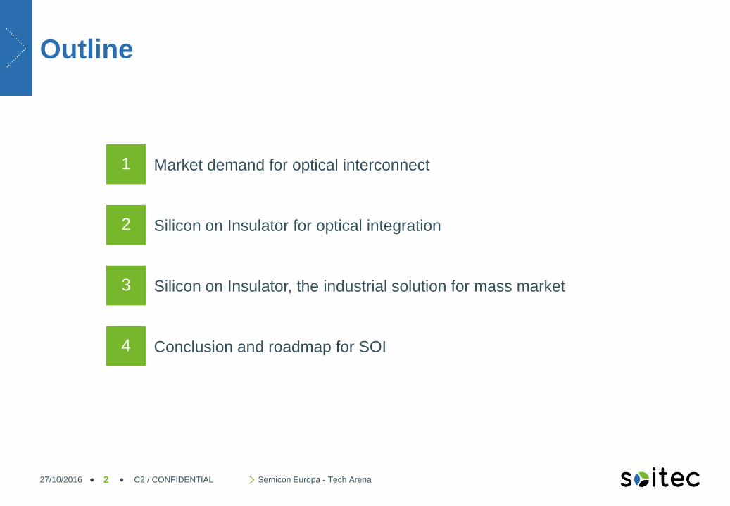
Interconnection within data center
Interconnection datarate is increasing : from 1Gb (2000) to 100G (2015)
27/10/2016 C2 / CONFIDENTIAL Semicon Europa - Tech Arena7
For speed of 10Gbs or higher
For reach of 1km
Optical communication is the most
efficient solutionSource: Ethernet Alliance, 2016
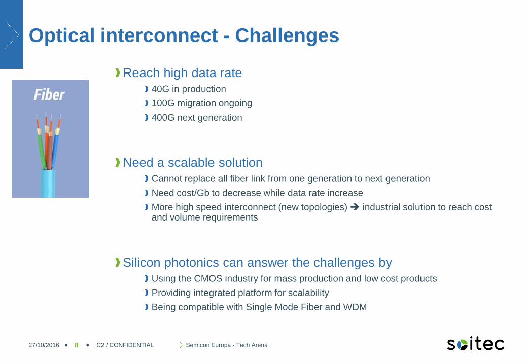
Optical interconnect - Challenges
Reach high data rate40G in production
100G migration ongoing
400G next generation
Need a scalable solutionCannot replace all fiber link from one generation to next generation
Need cost/Gb to decrease while data rate increase
More high speed interconnect (new topologies) industrial solution to reach cost and volume requirements
Silicon photonics can answer the challenges byUsing the CMOS industry for mass production and low cost products
Providing integrated platform for scalability
Being compatible with Single Mode Fiber and WDM
27/10/2016 C2 / CONFIDENTIAL Semicon Europa - Tech Arena8
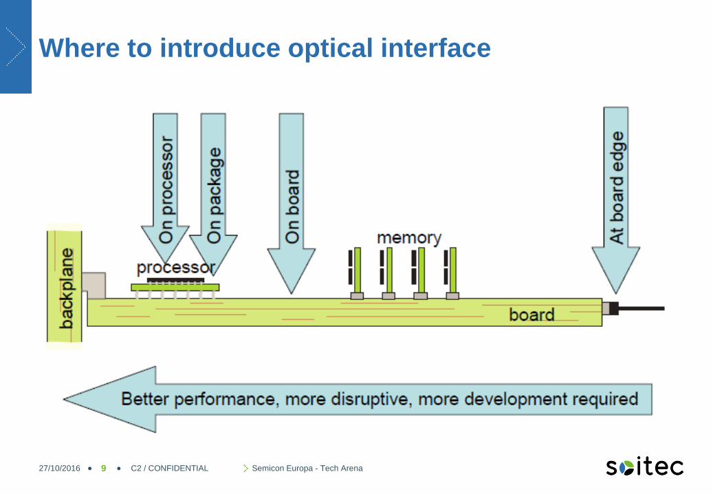
Where to introduce optical interface
27/10/2016 C2 / CONFIDENTIAL Semicon Europa - Tech Arena9
Silicon on Insulator for optical integration
27/10/2016 C2 / CONFIDENTIAL Semicon Europa - Tech Arena10
2
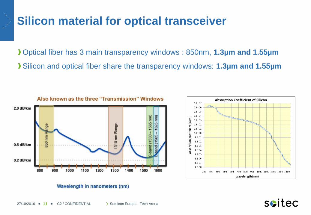
Silicon material for optical transceiver
Optical fiber has 3 main transparency windows : 850nm, 1.3µm and 1.55µm
Silicon and optical fiber share the transparency windows: 1.3µm and 1.55µm
27/10/2016 C2 / CONFIDENTIAL Semicon Europa - Tech Arena11
Mechanical support (silicon, …)
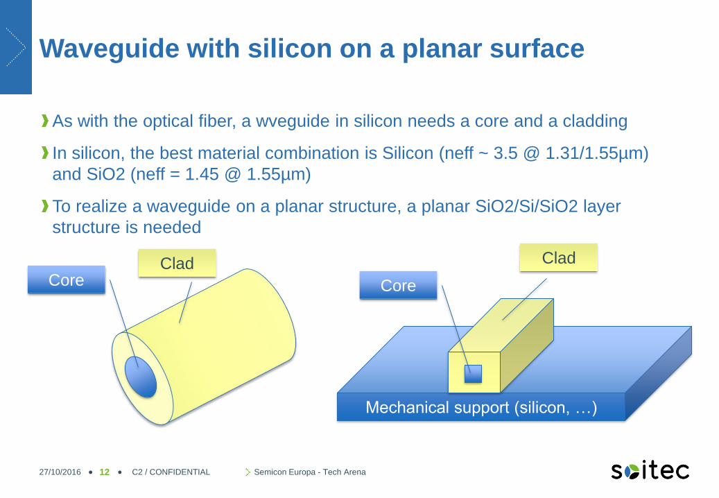
Waveguide with silicon on a planar surface
As with the optical fiber, a wveguide in silicon needs a core and a cladding
In silicon, the best material combination is Silicon (neff ~ 3.5 @ 1.31/1.55µm)
and SiO2 (neff = 1.45 @ 1.55µm)
To realize a waveguide on a planar structure, a planar SiO2/Si/SiO2 layer
structure is needed
27/10/2016 C2 / CONFIDENTIAL Semicon Europa - Tech Arena12
CoreClad
Core
Clad
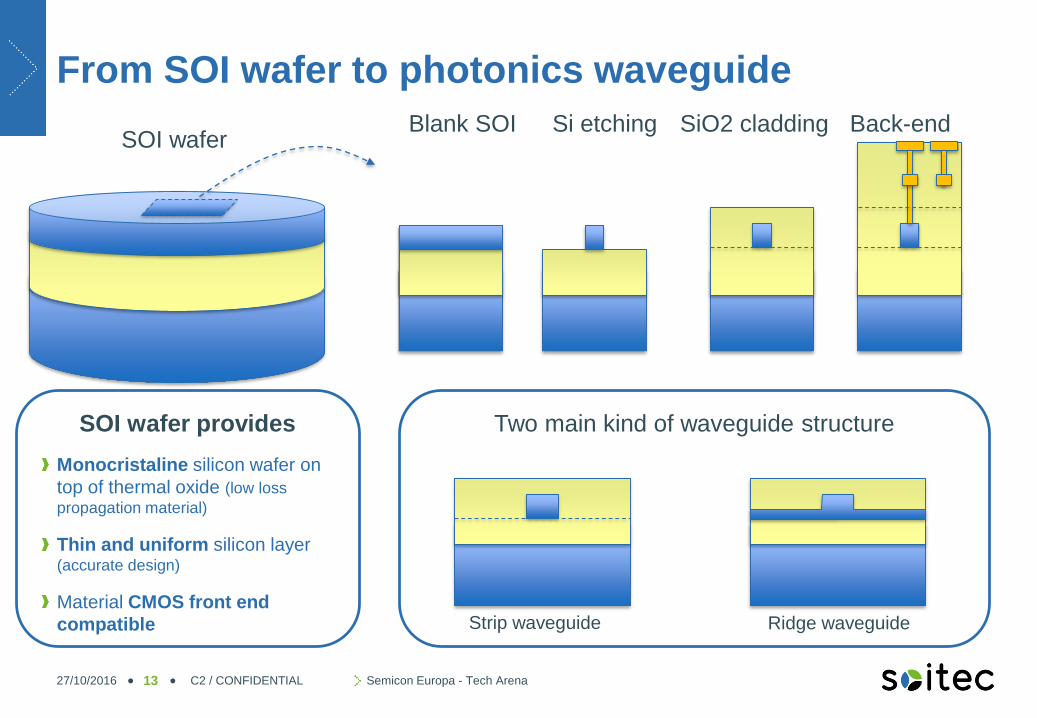
Two main kind of waveguide structure
From SOI wafer to photonics waveguide
27/10/2016 C2 / CONFIDENTIAL Semicon Europa - Tech Arena13
Blank SOI Si etching SiO2 cladding
Strip waveguide Ridge waveguide
SOI wafer
SOI wafer provides
Monocristaline silicon wafer on
top of thermal oxide (low loss
propagation material)
Thin and uniform silicon layer (accurate design)
Material CMOS front end
compatible
Back-end
From waveguide to devices
27/10/2016 C2 / CONFIDENTIAL Semicon Europa - Tech Arena14
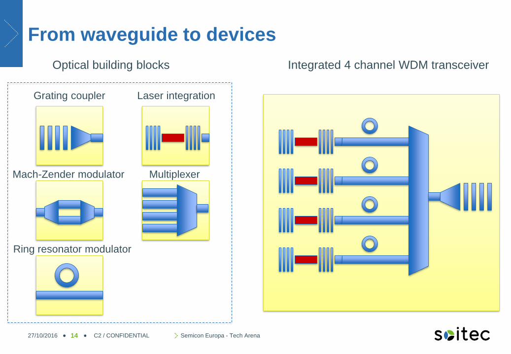
Grating coupler
Mach-Zender modulator
Ring resonator modulator
Laser integration
Multiplexer
Integrated 4 channel WDM transceiverOptical building blocks
Silicon photonics advantages compared to other
solutions
Integrated photonic device onto silicon, manufactured in a CMOS fab, enables
low cost mass production
Low loss propagation waveguide thanks to mono-crystalline top silicon layer
Small devices thanks to high index contrast between Silicon and oxide
Active device thanks to doping/back-end process
Compatible with single mode fiber (SMF)
Compatible with 1.3µm and 1.55µm optical windows
Scalability to increase bit rate per channel and wavelength multiplexing
Scalable solution to integrate optical transceiver close to the chip
27/10/2016 C2 / CONFIDENTIAL Semicon Europa - Tech Arena15
SOI is the platform of choice for silicon photonics
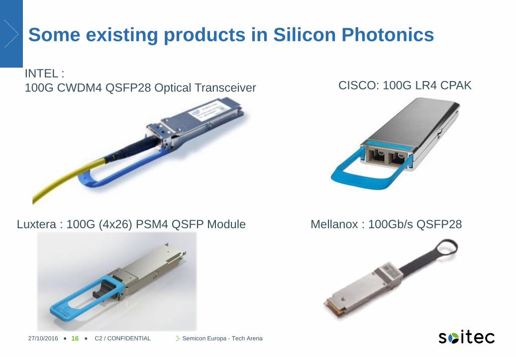
Some existing products in Silicon Photonics
27/10/2016 C2 / CONFIDENTIAL Semicon Europa - Tech Arena16
Luxtera : 100G (4x26) PSM4 QSFP Module
CISCO: 100G LR4 CPAKINTEL :
100G CWDM4 QSFP28 Optical Transceiver
Mellanox : 100Gb/s QSFP28

Silicon on Insulator, the industrial solution for mass market
27/10/2016 C2 / CONFIDENTIAL Semicon Europa - Tech Arena17
3
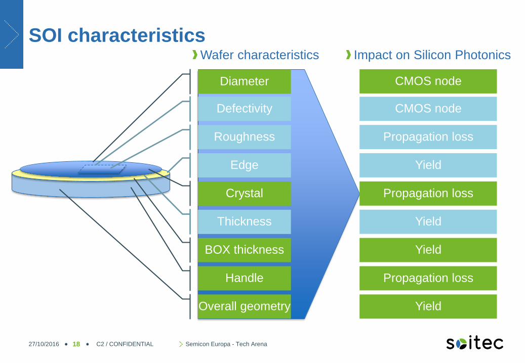
SOI characteristics
27/10/2016 C2 / CONFIDENTIAL Semicon Europa - Tech Arena18
Defectivity
Roughness
Edge
Crystal
Thickness
BOX thickness
Handle
Overall geometry
Wafer characteristics Impact on Silicon Photonics
CMOS node
Propagation loss
Yield
Propagation loss
Yield
Yield
Propagation loss
Yield
Diameter CMOS node
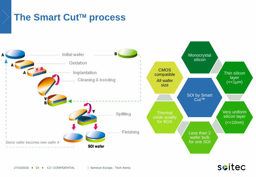
The Smart Cut process
27/10/2016 C2 / CONFIDENTIAL Semicon Europa - Tech Arena19
SOI by Smart Cut™
Monocrystalsilicon
Thin siliconlayer
(<<1µm)
Very uniformsilicon layer
(<<10nm)
Less than 2 wafer bulkfor one SOI
Thermal oxide quality
for BOX
CMOS compatible
All wafer size
Oxidation
Donor wafer becomes new wafer A
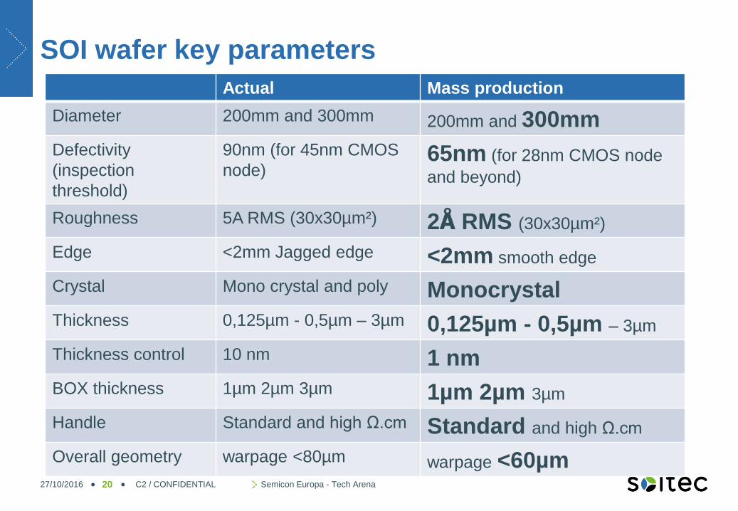
SOI wafer key parameters
27/10/2016 C2 / CONFIDENTIAL Semicon Europa - Tech Arena20
Actual Mass production
Diameter 200mm and 300mm 200mm and 300mm
Defectivity
(inspection
threshold)
90nm (for 45nm CMOS
node)65nm (for 28nm CMOS node
and beyond)
Roughness 5A RMS (30x30µm²) 2Å RMS (30x30µm²)
Edge <2mm Jagged edge <2mm smooth edge
Crystal Mono crystal and poly Monocrystal
Thickness 0,125µm - 0,5µm – 3µm 0,125µm - 0,5µm – 3µm
Thickness control 10 nm 1 nm
BOX thickness 1µm 2µm 3µm 1µm 2µm 3µm
Handle Standard and high Ω.cm Standard and high Ω.cm
Overall geometry warpage <80µm warpage <60µm
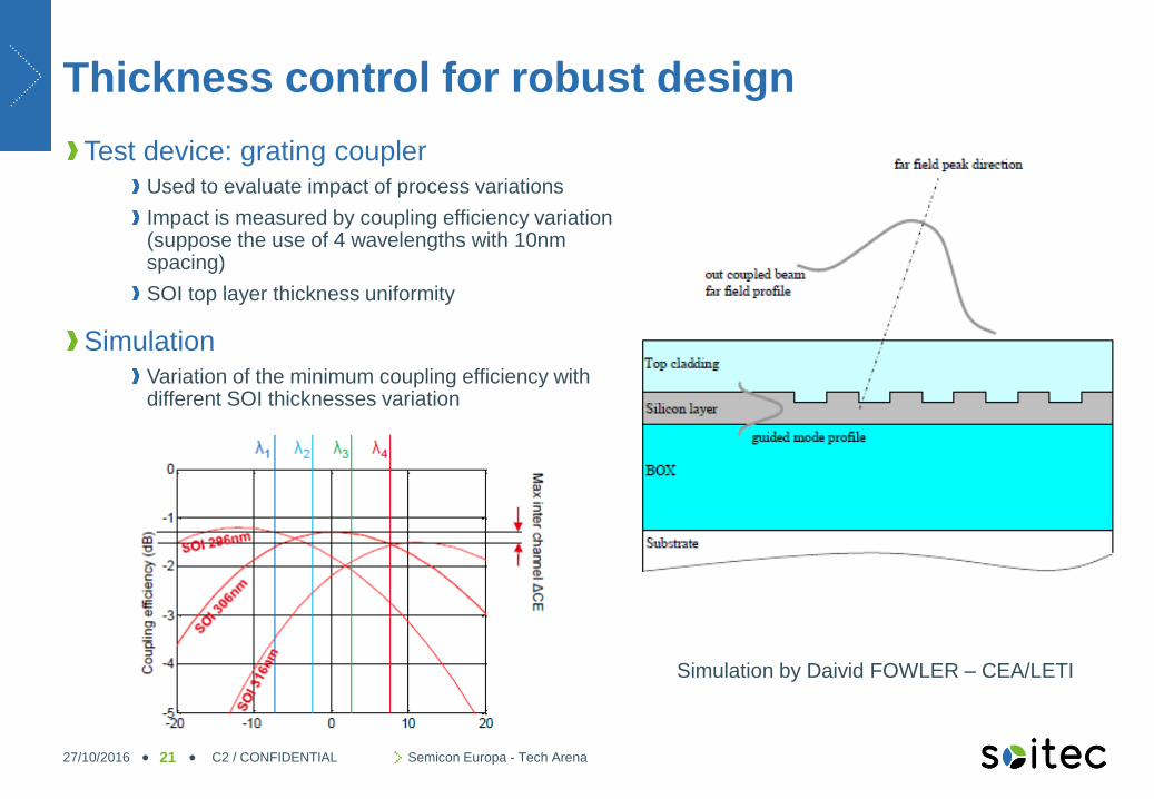
Thickness control for robust design
Test device: grating couplerUsed to evaluate impact of process variations
Impact is measured by coupling efficiency variation (suppose the use of 4 wavelengths with 10nm spacing)
SOI top layer thickness uniformity
SimulationVariation of the minimum coupling efficiency with different SOI thicknesses variation
27/10/2016 C2 / CONFIDENTIAL Semicon Europa - Tech Arena21
Simulation by Daivid FOWLER – CEA/LETI
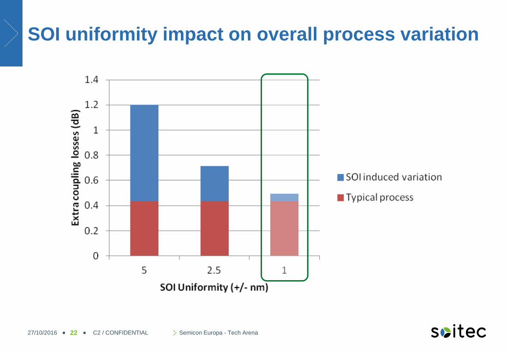
SOI uniformity impact on overall process variation
27/10/2016 C2 / CONFIDENTIAL Semicon Europa - Tech Arena22
Thermal smoothing processCMP (polishing) process
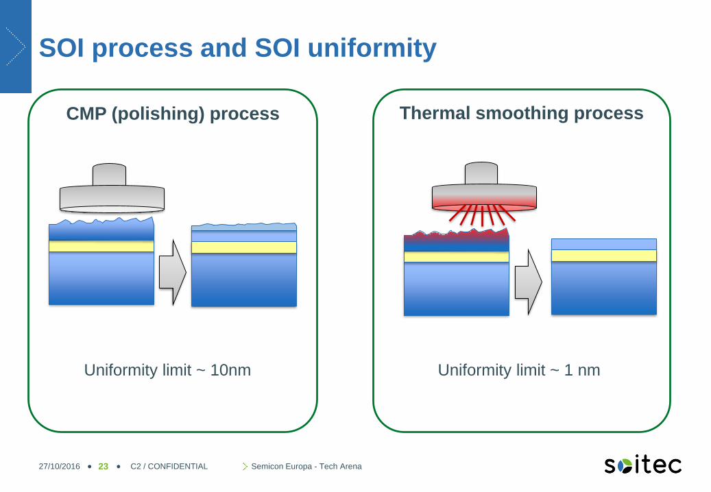
SOI process and SOI uniformity
27/10/2016 C2 / CONFIDENTIAL Semicon Europa - Tech Arena23
Uniformity limit ~ 10nm Uniformity limit ~ 1 nm

Thermal smoothing principle
Silicon surface smoothing at high temperature (RTA, BA)Material transport mechanism
Bulk diffusion
Evaporation / Condensation
Surface diffusion
27/10/2016 C2 / CONFIDENTIAL Semicon Europa - Tech Arena24
Silicon
Gas
Bulk diffusion
Evaporation / condensation
Surface diffusion
Reaction with
contaminant
F.De Crecy – CEA/LETI
Simulation of silicon smoothing under high temp anneal
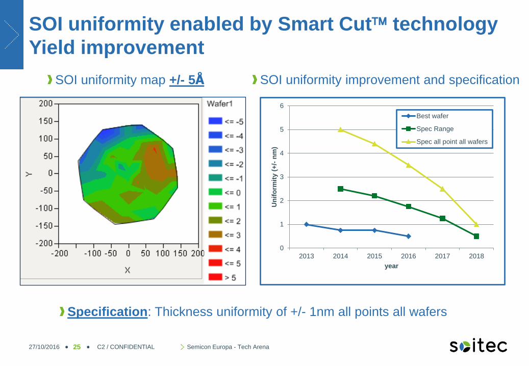
SOI uniformity enabled by Smart Cut technology
Yield improvement
27/10/2016 C2 / CONFIDENTIAL Semicon Europa - Tech Arena25
SOI uniformity map +/- 5Å
0
1
2
3
4
5
6
2013 2014 2015 2016 2017 2018
Un
ifo
rmit
y (
+/-
nm
)
year
Best wafer
Spec Range
Spec all point all wafers
SOI uniformity improvement and specification
Specification: Thickness uniformity of +/- 1nm all points all wafers
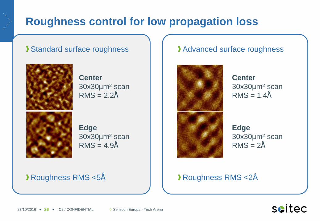
Roughness control for low propagation loss
Standard surface roughness
Roughness RMS <5Å
27/10/2016 C2 / CONFIDENTIAL Semicon Europa - Tech Arena26
Advanced surface roughness
Roughness RMS <2Å
Center
30x30µm² scan
RMS = 2.2Å
Edge
30x30µm² scan
RMS = 4.9Å
Center
30x30µm² scan
RMS = 1.4Å
Edge
30x30µm² scan
RMS = 2Å
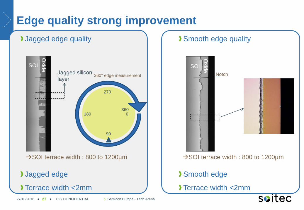
Smooth edge quality
Smooth edge
Terrace width <2mm
Edge quality strong improvement
27/10/2016 C2 / CONFIDENTIAL Semicon Europa - Tech Arena27
Jagged edge quality
Jagged edge
Terrace width <2mm
0
90
180
270
360
SOI terrace width : 800 to 1200µm
Notch
SOI terrace width : 800 to 1200µm
360° edge measurementJagged silicon
layer
SOI
Oxid
e SOI
Oxid
e
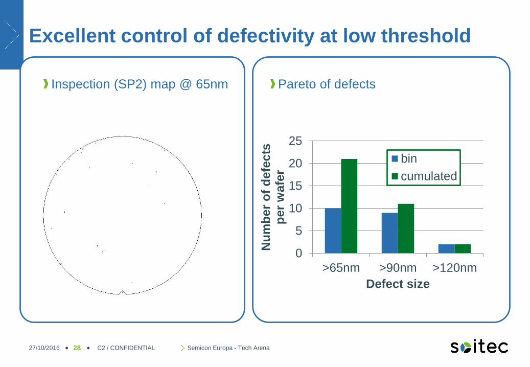
Excellent control of defectivity at low threshold
27/10/2016 C2 / CONFIDENTIAL Semicon Europa - Tech Arena28
0
5
10
15
20
25
>65nm >90nm >120nmN
um
ber
of
defe
cts
p
er
wafe
rDefect size
bin
cumulated
Inspection (SP2) map @ 65nm Pareto of defects
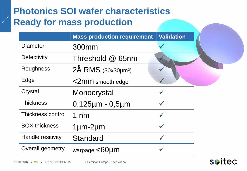
Photonics SOI wafer characteristics
Ready for mass production
27/10/2016 C2 / CONFIDENTIAL Semicon Europa - Tech Arena29
Mass production requirement Validation
Diameter 300mm
Defectivity Threshold @ 65nm
Roughness 2Å RMS (30x30µm²)
Edge <2mm smooth edge
Crystal Monocrystal
Thickness 0,125µm - 0,5µm
Thickness control 1 nm
BOX thickness 1µm-2µm
Handle resitivity Standard
Overall geometry warpage <60µm

Conclusion
27/10/2016 C2 / CONFIDENTIAL Semicon Europa - Tech Arena30
4
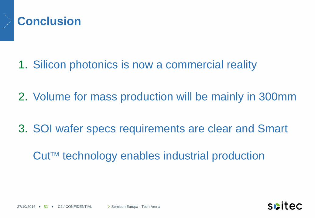
Conclusion
1. Silicon photonics is now a commercial reality
2. Volume for mass production will be mainly in 300mm
3. SOI wafer specs requirements are clear and Smart
Cut technology enables industrial production
27/10/2016 C2 / CONFIDENTIAL Semicon Europa - Tech Arena31

27/10/2016 C2 / CONFIDENTIAL Semicon Europa - Tech Arena32 SOI enables next generation data centersSource: Reuters, "Chanel Data Center", Karl Lagerfeld

Thank you for you attention
27/10/2016 C2 / CONFIDENTIAL Semicon Europa - Tech Arena33
© Exclusive property of Soitec. This document contains confidential information.
Disclosure, redisclosure, dissemination, redissemination, reproduction or use is
limited to authorized persons only. Disclosure to third parties requires a Non
Disclosure Agreement. Use or reuse, in whole or in part, by any means and in any
form, for any purpose other than which is expressly set forth in this document is
forbidden.
Disclaimer
27/10/2016 C2 / CONFIDENTIAL Semicon Europa - Tech Arena34