Embed Size (px)
Citation preview
IEEE
Proo
f
JOURNAL OF LIGHTWAVE TECHNOLOGY 1
Techno-Economic Comparison of SiliconPhotonics and Multimode VCSELs
Daniel Mahgerefteh, Craig Thompson, Chris Cole, Gilles Denoyer, Thelinh Nguyen,Ilya Lyubomirsky, Chris Kocot, and Jim Tatum
(Invited Paper)
Abstract—Recent technical and commercial milestones in SiliconPhotonics technology including its introduction into commercialfoundries, and successful integration of most optical components,as well as the choice of single mode fiber in some mega data cen-ters have prompted the speculation that Si photonics is the newlow cost solution for optical interconnects and that it may replacemulti-mode vertical cavity surface emitting lasers (MM VCSEL).We show that the dominant technology has to offer the lowest costfor the single channel transceiver application, which represents90% of the data center market and which historically dominatessales. We show that Si photonics is currently significantly more ex-pensive than MM VCSEL for single channel, but that it can makea successful entry into the four channel single mode market withsignificant growth, capturing 20% of the data center market. Wediscuss the challenges with Si/InP integration; i.e., hybrid lasers forbreaking the cost barrier and to enter the market. We show thatboth MM VCSEL and Si photonics technologies can operate at50 Gb/s. We discuss the transmission reach limitations of Si pho-tonics and MM VCSEL and show an example of reach extension for100 Gb/s using MM VCSEL to 300 m of MM fiber. In addition weshow that MM VCSEL has fundamentally lower power consump-tion than Si photonics and is a good candidate for super-computingapplications.
Index Terms—Multimode Vertical Cavity Surface EmittingLaser, data centers, hybrid lasers, Silicon Photonics.
I. INTRODUCTION
S ILICON Photonics has been in the spotlight in recent yearswith a number of technological and commercial highlights.
Active optical cables (AOCs) and “pigtailed” transceivers using4 × 10 Gb/s silicon (Si) photonic integrated circuits (PIC) havebeen in the market for a few years [1]. A number of commer-cial CMOS foundries including IBM and ST Microelectronicsare adding Si photonics into their manufacturing lines, and re-searchers have shown that most optical functions, save the laserand isolator, can be integrated in Si [2]–[4]. Some new mega-data centers are being designed with single mode (SM) fiberinfrastructure cabling, opening a market for Si photonics. Thesetechnical and commercial milestones, as well as the old adage,
Manuscript received July 8, 2015; revised August 21, 2015; accepted Septem-ber 11, 2015.
The authors are with the Finisar Corporation, Sunnyvale, CA 94089 USA(e-mail: [email protected]; [email protected]; [email protected]; [email protected]; [email protected];[email protected]; [email protected]; [email protected]).
Color versions of one or more of the figures in this paper are available onlineat http://ieeexplore.ieee.org.
Digital Object Identifier 10.1109/JLT.2015.2483587
“If you compete with CMOS, don’t!” have prompted the specu-lation that Si photonics is the new low cost solution for opticalinterconnects. Is Si photonics the future of optical interconnectsand will it replace MM VCSELs? We attempt to answer thisquestion by comparing Si photonics and MM VCSELs basedon their applicable markets, relative costs, transmission reach,power consumption, and bandwidth-density.
Cost is particularly important for data center applications be-cause optical interconnects are becoming a significant part ofthe total bill of materials. The massive parallelism imposed bythe architectures used increases the number of interconnectsbetween switches and increases the average link length whichrequire the more expensive single-mode transceivers thereby in-creasing the total cost of interconnects between them. Also theservers, memory, and electrical packet switches used in thesesystems have benefitted from high volume, mature CMOS tech-nology, which uses wafer level processes, test, and packaging, soit is assumed that optics can similarly benefit. We will examinethis premise here.
In Section II we make a comparison of the application spaceand cost structure of Si photonics and multi-mode VCSEL fordata center applications. We will show that the majority of thetransceiver volume is in single channel form, which biases thecost competition between the technologies in favor of 850 nmMM VCSEL or 1310 nm directly modulated lasers (DMLs). InSection III we explain why single channel is the dominant formfactor today and explore its future. In Section IV we show thatSi photonics has a large and growing market opportunity in thefour channel parallel (PSM4) and course wavelength divisionmultiplexing (CWDM) applications spaces which are especiallysuited to the mega data centers. In Sections V and VI we showthat both Si photonics and MM VCSEL, respectively, can oper-ate at 50 Gb/s. In Section VII we discuss limitation to the trans-mission reach of Si photonics. In Section VIII we discuss thereach limitation of MM VCSEL and present an example of reachextension to 300 m for at 100 Gb/s for. In Section IX we comparethe power consumption of high speed VCSEL and Si photonicstransmitters and show that VCSELs have fundamentally lowerpower consumption, and we conclude with Section X.
II. VOLUME AND COST
Multimode VCSELs operating on multimode fiber are dom-inating short reach links in data centers today because they arethe lowest cost. The reasons for the current cost difference be-tween Si photonics and MM VCSEL are part economics andpart technical. In this section we focus on the economic side.
0733-8724 © 2015 IEEE. Personal use is permitted, but republication/redistribution requires IEEE permission.See http://www.ieee.org/publications standards/publications/rights/index.html for more information.
IEEE
Proo
f
2 JOURNAL OF LIGHTWAVE TECHNOLOGY
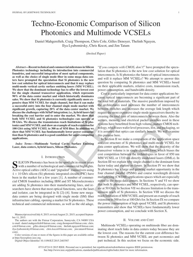
Fig. 1. Application space in current data centers based on (a) transmissionreach and fiber type, (b) loss budget, or (c) technology.
Fig. 2. Distribution of OM4 MM trunk fiber cables manufactured between1/2012 and 12/2014 versus length. Line is accumulated percentage. (Courtesyof Corning Corporation).
Costs drop when volumes increase, especially when the man-ufacturing technology has a high up-front capital expenditureassociated with it (such as CMOS fabrication), so comparisonof the two technologies has to be made for the applications withthe highest volumes.
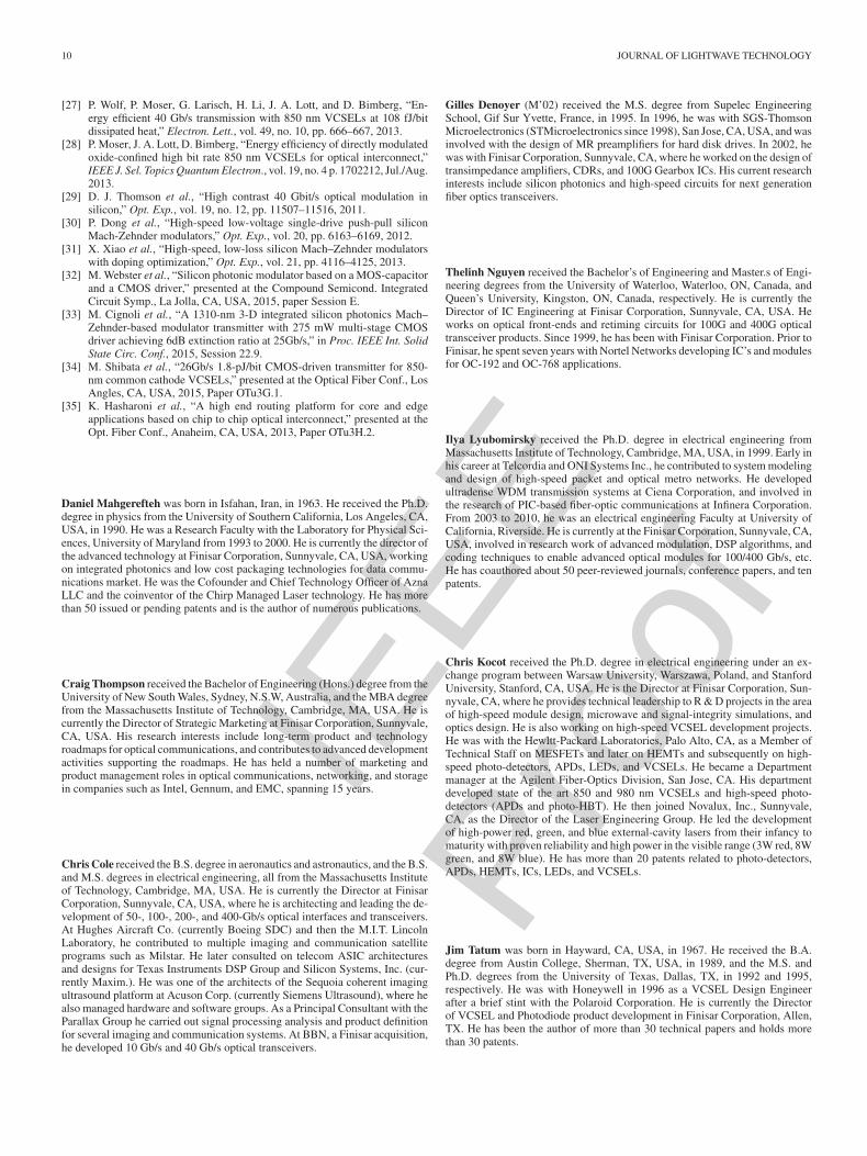
The data communication application space is currently parsedout by transmission reach and fiber type, multi-mode fiber(MMF), or SM fiber (SMF), and loss budget for the opticallink, and is currently dominated by MM VCSEL and DML tech-nologies (see Fig. 1). The loss budget and transmission reach areestablished by various communications standards such as IEEE,TIA, etc., and are based on industry consensus on available tech-nology that is expected to be manufactured at the lowest cost.Since we are trying to compare the highest volume applicationsfor cost, we will focus on the IEEE Ethernet 802.3ae. Until re-cently there were only two sets of standards: 1) The short reach(SR) standards intended for MM 850 nm VCSEL for 300 m at10 Gb/s and 100 m for 100 Gb/s and 2) The long reach (LR)standard intended for SM fiber at 1310 nm for 0–10 km and achannel insertion loss of 6.2 dB. Fig. 1 also shows a 2000 m SMfiber reach with 3–4 dB loss budget, which represents the newermega data center application and is currently being addressedthrough industry multi-source agreements (MSAs).
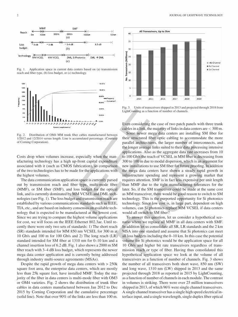
Despite the rapid growth of mega data centers with > 250ksquare foot area, the enterprise data centers, which are mostlyless than 25k square feet, have installed MMF. Today the ma-jority of the fiber in data centers is multi-mode fiber with OM3or OM4 varieties. Fig. 2 shows the distribution of trunk fibercables in data centers manufactured between Jan 2012 to Dec2015 by Corning Corporation and the cumulative percentage(solid line). Note that over 90% of the links are less than 100 m.
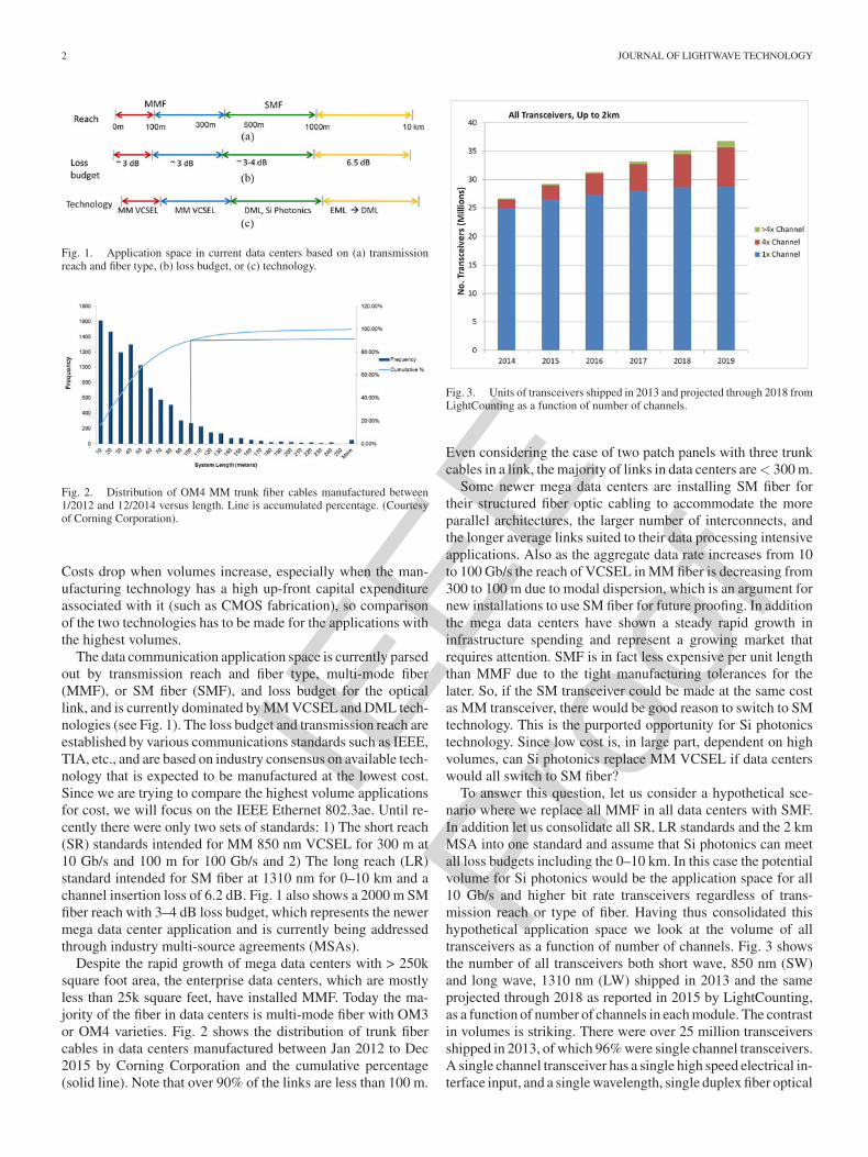
Fig. 3. Units of transceivers shipped in 2013 and projected through 2018 fromLightCounting as a function of number of channels.
Even considering the case of two patch panels with three trunkcables in a link, the majority of links in data centers are < 300 m.
Some newer mega data centers are installing SM fiber fortheir structured fiber optic cabling to accommodate the moreparallel architectures, the larger number of interconnects, andthe longer average links suited to their data processing intensiveapplications. Also as the aggregate data rate increases from 10to 100 Gb/s the reach of VCSEL in MM fiber is decreasing from300 to 100 m due to modal dispersion, which is an argument fornew installations to use SM fiber for future proofing. In additionthe mega data centers have shown a steady rapid growth ininfrastructure spending and represent a growing market thatrequires attention. SMF is in fact less expensive per unit lengththan MMF due to the tight manufacturing tolerances for thelater. So, if the SM transceiver could be made at the same costas MM transceiver, there would be good reason to switch to SMtechnology. This is the purported opportunity for Si photonicstechnology. Since low cost is, in large part, dependent on highvolumes, can Si photonics replace MM VCSEL if data centerswould all switch to SM fiber?
To answer this question, let us consider a hypothetical sce-nario where we replace all MMF in all data centers with SMF.In addition let us consolidate all SR, LR standards and the 2 kmMSA into one standard and assume that Si photonics can meetall loss budgets including the 0–10 km. In this case the potentialvolume for Si photonics would be the application space for all10 Gb/s and higher bit rate transceivers regardless of trans-mission reach or type of fiber. Having thus consolidated thishypothetical application space we look at the volume of alltransceivers as a function of number of channels. Fig. 3 showsthe number of all transceivers both short wave, 850 nm (SW)and long wave, 1310 nm (LW) shipped in 2013 and the sameprojected through 2018 as reported in 2015 by LightCounting,as a function of number of channels in each module. The contrastin volumes is striking. There were over 25 million transceiversshipped in 2013, of which 96% were single channel transceivers.A single channel transceiver has a single high speed electrical in-terface input, and a single wavelength, single duplex fiber optical
IEEE
Proo
f
MAHGEREFTEH et al.: TECHNO-ECONOMIC COMPARISON OF SILICON PHOTONICS AND MULTIMODE VCSELS 3
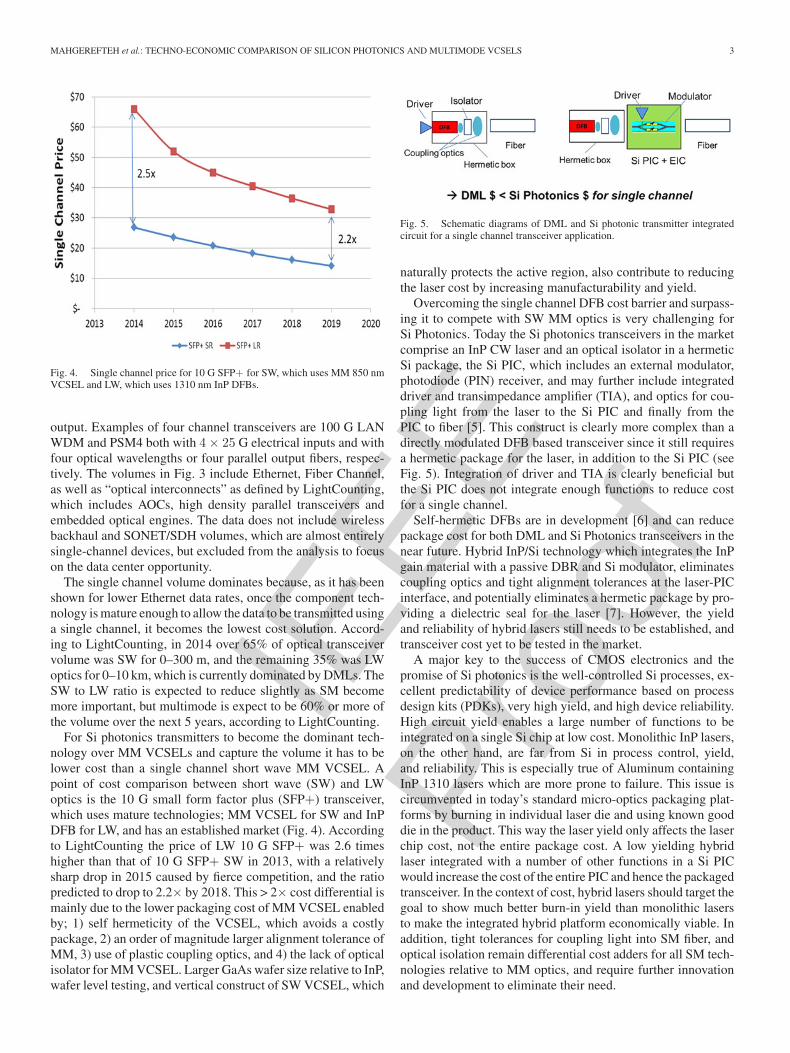
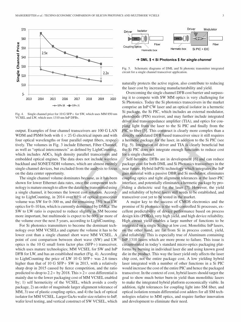
Fig. 4. Single channel price for 10 G SFP+ for SW, which uses MM 850 nmVCSEL and LW, which uses 1310 nm InP DFBs.
output. Examples of four channel transceivers are 100 G LANWDM and PSM4 both with 4 × 25 G electrical inputs and withfour optical wavelengths or four parallel output fibers, respec-tively. The volumes in Fig. 3 include Ethernet, Fiber Channel,as well as “optical interconnects” as defined by LightCounting,which includes AOCs, high density parallel transceivers andembedded optical engines. The data does not include wirelessbackhaul and SONET/SDH volumes, which are almost entirelysingle-channel devices, but excluded from the analysis to focuson the data center opportunity.
The single channel volume dominates because, as it has beenshown for lower Ethernet data rates, once the component tech-nology is mature enough to allow the data to be transmitted usinga single channel, it becomes the lowest cost solution. Accord-ing to LightCounting, in 2014 over 65% of optical transceivervolume was SW for 0–300 m, and the remaining 35% was LWoptics for 0–10 km, which is currently dominated by DMLs. TheSW to LW ratio is expected to reduce slightly as SM becomemore important, but multimode is expect to be 60% or more ofthe volume over the next 5 years, according to LightCounting.
For Si photonics transmitters to become the dominant tech-nology over MM VCSELs and capture the volume it has to belower cost than a single channel short wave MM VCSEL. Apoint of cost comparison between short wave (SW) and LWoptics is the 10 G small form factor plus (SFP+) transceiver,which uses mature technologies; MM VCSEL for SW and InPDFB for LW, and has an established market (Fig. 4). Accordingto LightCounting the price of LW 10 G SFP+ was 2.6 timeshigher than that of 10 G SFP+ SW in 2013, with a relativelysharp drop in 2015 caused by fierce competition, and the ratiopredicted to drop to 2.2× by 2018. This > 2× cost differential ismainly due to the lower packaging cost of MM VCSEL enabledby; 1) self hermeticity of the VCSEL, which avoids a costlypackage, 2) an order of magnitude larger alignment tolerance ofMM, 3) use of plastic coupling optics, and 4) the lack of opticalisolator for MM VCSEL. Larger GaAs wafer size relative to InP,wafer level testing, and vertical construct of SW VCSEL, which
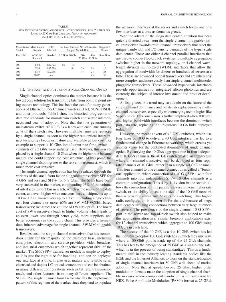
Fig. 5. Schematic diagrams of DML and Si photonic transmitter integratedcircuit for a single channel transceiver application.
naturally protects the active region, also contribute to reducingthe laser cost by increasing manufacturability and yield.
Overcoming the single channel DFB cost barrier and surpass-ing it to compete with SW MM optics is very challenging forSi Photonics. Today the Si photonics transceivers in the marketcomprise an InP CW laser and an optical isolator in a hermeticSi package, the Si PIC, which includes an external modulator,photodiode (PIN) receiver, and may further include integrateddriver and transimpedance amplifier (TIA), and optics for cou-pling light from the laser to the Si PIC and finally from thePIC to fiber [5]. This construct is clearly more complex than adirectly modulated DFB based transceiver since it still requiresa hermetic package for the laser, in addition to the Si PIC (seeFig. 5). Integration of driver and TIA is clearly beneficial butthe Si PIC does not integrate enough functions to reduce costfor a single channel.
Self-hermetic DFBs are in development [6] and can reducepackage cost for both DML and Si Photonics transceivers in thenear future. Hybrid InP/Si technology which integrates the InPgain material with a passive DBR and Si modulator, eliminatescoupling optics and tight alignment tolerances at the laser-PICinterface, and potentially eliminates a hermetic package by pro-viding a dielectric seal for the laser [7]. However, the yieldand reliability of hybrid lasers still needs to be established, andtransceiver cost yet to be tested in the market.
A major key to the success of CMOS electronics and thepromise of Si photonics is the well-controlled Si processes, ex-cellent predictability of device performance based on processdesign kits (PDKs), very high yield, and high device reliability.High circuit yield enables a large number of functions to beintegrated on a single Si chip at low cost. Monolithic InP lasers,on the other hand, are far from Si in process control, yield,and reliability. This is especially true of Aluminum containingInP 1310 lasers which are more prone to failure. This issue iscircumvented in today’s standard micro-optics packaging plat-forms by burning in individual laser die and using known gooddie in the product. This way the laser yield only affects the laserchip cost, not the entire package cost. A low yielding hybridlaser integrated with a number of other functions in a Si PICwould increase the cost of the entire PIC and hence the packagedtransceiver. In the context of cost, hybrid lasers should target thegoal to show much better burn-in yield than monolithic lasersto make the integrated hybrid platform economically viable. Inaddition, tight tolerances for coupling light into SM fiber, andoptical isolation remain differential cost adders for all SM tech-nologies relative to MM optics, and require further innovationand development to eliminate their need.
IEEE
Proo
f
4 JOURNAL OF LIGHTWAVE TECHNOLOGY
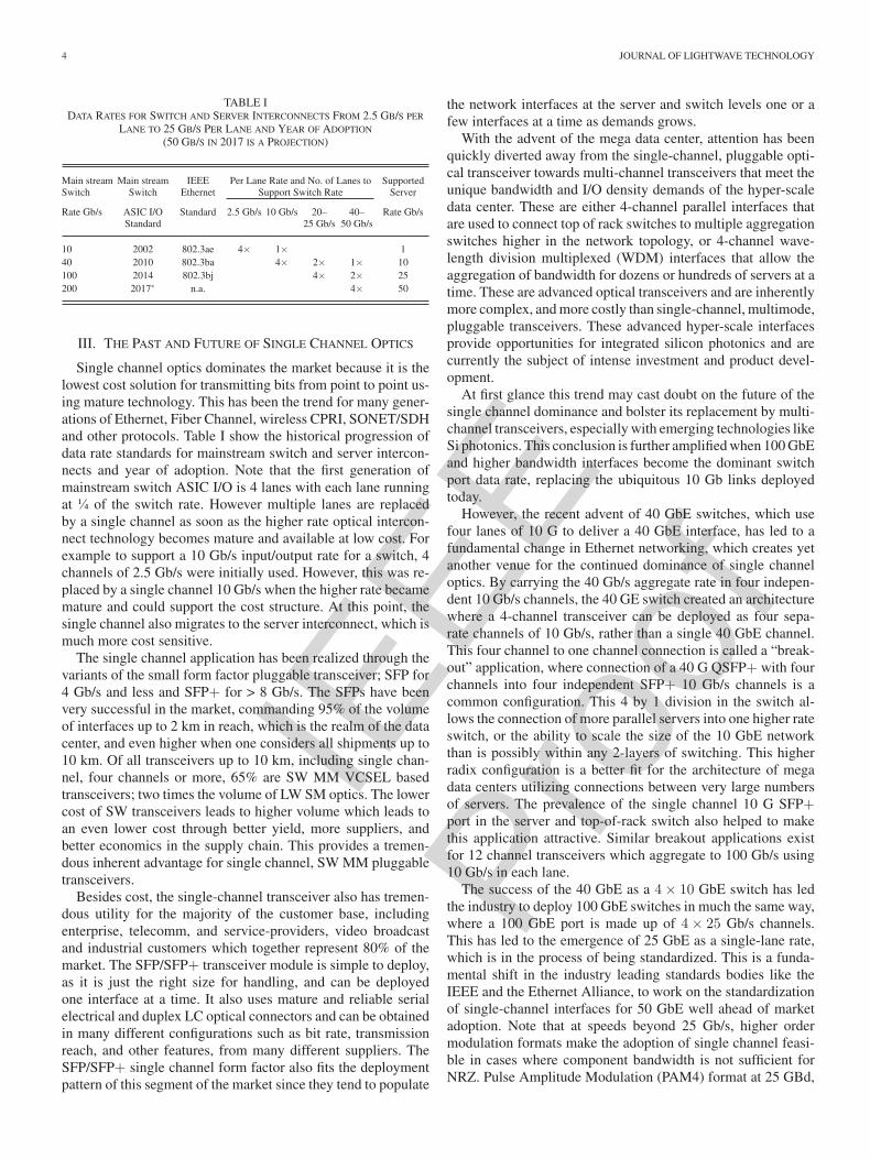
TABLE IDATA RATES FOR SWITCH AND SERVER INTERCONNECTS FROM 2.5 GB/S PER
LANE TO 25 GB/S PER LANE AND YEAR OF ADOPTION
(50 GB/S IN 2017 IS A PROJECTION)
Main streamSwitch
Main streamSwitch
IEEEEthernet
Per Lane Rate and No. of Lanes toSupport Switch Rate
SupportedServer
Rate Gb/s ASIC I/OStandard
Standard 2.5 Gb/s 10 Gb/s 20–25 Gb/s
40–50 Gb/s
Rate Gb/s
10 2002 802.3ae 4× 1× 140 2010 802.3ba 4× 2× 1× 10100 2014 802.3bj 4× 2× 25200 2017∗ n.a. 4× 50
III. THE PAST AND FUTURE OF SINGLE CHANNEL OPTICS
Single channel optics dominates the market because it is thelowest cost solution for transmitting bits from point to point us-ing mature technology. This has been the trend for many gener-ations of Ethernet, Fiber Channel, wireless CPRI, SONET/SDHand other protocols. Table I show the historical progression ofdata rate standards for mainstream switch and server intercon-nects and year of adoption. Note that the first generation ofmainstream switch ASIC I/O is 4 lanes with each lane runningat ¼ of the switch rate. However multiple lanes are replacedby a single channel as soon as the higher rate optical intercon-nect technology becomes mature and available at low cost. Forexample to support a 10 Gb/s input/output rate for a switch, 4channels of 2.5 Gb/s were initially used. However, this was re-placed by a single channel 10 Gb/s when the higher rate becamemature and could support the cost structure. At this point, thesingle channel also migrates to the server interconnect, which ismuch more cost sensitive.
The single channel application has been realized through thevariants of the small form factor pluggable transceiver; SFP for4 Gb/s and less and SFP+ for > 8 Gb/s. The SFPs have beenvery successful in the market, commanding 95% of the volumeof interfaces up to 2 km in reach, which is the realm of the datacenter, and even higher when one considers all shipments up to10 km. Of all transceivers up to 10 km, including single chan-nel, four channels or more, 65% are SW MM VCSEL basedtransceivers; two times the volume of LW SM optics. The lowercost of SW transceivers leads to higher volume which leads toan even lower cost through better yield, more suppliers, andbetter economics in the supply chain. This provides a tremen-dous inherent advantage for single channel, SW MM pluggabletransceivers.
Besides cost, the single-channel transceiver also has tremen-dous utility for the majority of the customer base, includingenterprise, telecomm, and service-providers, video broadcastand industrial customers which together represent 80% of themarket. The SFP/SFP+ transceiver module is simple to deploy,as it is just the right size for handling, and can be deployedone interface at a time. It also uses mature and reliable serialelectrical and duplex LC optical connectors and can be obtainedin many different configurations such as bit rate, transmissionreach, and other features, from many different suppliers. TheSFP/SFP+ single channel form factor also fits the deploymentpattern of this segment of the market since they tend to populate
the network interfaces at the server and switch levels one or afew interfaces at a time as demands grows.
With the advent of the mega data center, attention has beenquickly diverted away from the single-channel, pluggable opti-cal transceiver towards multi-channel transceivers that meet theunique bandwidth and I/O density demands of the hyper-scaledata center. These are either 4-channel parallel interfaces thatare used to connect top of rack switches to multiple aggregationswitches higher in the network topology, or 4-channel wave-length division multiplexed (WDM) interfaces that allow theaggregation of bandwidth for dozens or hundreds of servers at atime. These are advanced optical transceivers and are inherentlymore complex, and more costly than single-channel, multimode,pluggable transceivers. These advanced hyper-scale interfacesprovide opportunities for integrated silicon photonics and arecurrently the subject of intense investment and product devel-opment.
At first glance this trend may cast doubt on the future of thesingle channel dominance and bolster its replacement by multi-channel transceivers, especially with emerging technologies likeSi photonics. This conclusion is further amplified when 100 GbEand higher bandwidth interfaces become the dominant switchport data rate, replacing the ubiquitous 10 Gb links deployedtoday.
However, the recent advent of 40 GbE switches, which usefour lanes of 10 G to deliver a 40 GbE interface, has led to afundamental change in Ethernet networking, which creates yetanother venue for the continued dominance of single channeloptics. By carrying the 40 Gb/s aggregate rate in four indepen-dent 10 Gb/s channels, the 40 GE switch created an architecturewhere a 4-channel transceiver can be deployed as four sepa-rate channels of 10 Gb/s, rather than a single 40 GbE channel.This four channel to one channel connection is called a “break-out” application, where connection of a 40 G QSFP+ with fourchannels into four independent SFP+ 10 Gb/s channels is acommon configuration. This 4 by 1 division in the switch al-lows the connection of more parallel servers into one higher rateswitch, or the ability to scale the size of the 10 GbE networkthan is possibly within any 2-layers of switching. This higherradix configuration is a better fit for the architecture of megadata centers utilizing connections between very large numbersof servers. The prevalence of the single channel 10 G SFP+port in the server and top-of-rack switch also helped to makethis application attractive. Similar breakout applications existfor 12 channel transceivers which aggregate to 100 Gb/s using10 Gb/s in each lane.
The success of the 40 GbE as a 4 × 10 GbE switch has ledthe industry to deploy 100 GbE switches in much the same way,where a 100 GbE port is made up of 4 × 25 Gb/s channels.This has led to the emergence of 25 GbE as a single-lane rate,which is in the process of being standardized. This is a funda-mental shift in the industry leading standards bodies like theIEEE and the Ethernet Alliance, to work on the standardizationof single-channel interfaces for 50 GbE well ahead of marketadoption. Note that at speeds beyond 25 Gb/s, higher ordermodulation formats make the adoption of single channel feasi-ble in cases where component bandwidth is not sufficient forNRZ. Pulse Amplitude Modulation (PAM4) format at 25 GBd,
IEEE
Proo
f
MAHGEREFTEH et al.: TECHNO-ECONOMIC COMPARISON OF SILICON PHOTONICS AND MULTIMODE VCSELS 5
Fig. 6. Number of channels shipped in all transceivers and projections for allreaches between 0–2 km from LightCounting. (blue) all SW optics for 0–300 mMM fiber, (red) all LW optics for 0–2 km SM fiber.
for example, enables a single electrical and optical channel at50 Gb/s.
With the industry beginning to focus on single-channel inter-faces at 50 Gb/s, it became clear that a single-channel/4-channelroadmap for 50 G per channel can have the same benefits of-fered by the 10 G/40 G and 25 G/100 G use-cases. Momentumis now building to create a 200 GbE standard from 4 × 50 G,as well as a 4 × 100 G interface for 400 GbE as a post-cursorfor 8 × 50 G. This means that at least 4 generations of 1-channel /4-channel transceiver pairings up to 400 GbE (10/40,25/100, 50/200, 100/400) are possible. Beyond the 10 G SFP+ transceiver, it is conceivable that at least 3 more generationsof SFPx transceiver will exist. The industry is already adoptingSFP28 for single-channel transceivers with continued strong de-mand for low-cost multimode versions of the form factor. Thesefaster transitions in the Ethernet single-channel lane speed beginto mirror the bandwidth transitions in the Fibre Channel market;doubling bandwidth per channel every 5 years.
Assuming the dominance of single-channel transceivers con-tinues with 25 GBE, and the clear cost and volume advantagesof multimode single-channel transceivers, we believe MM VC-SELs can continue to enjoy high volumes and provide the lowestcost for short reach data center applications for some time tocome.
IV. THE SILICON PHOTONICS OPPORTUNITY
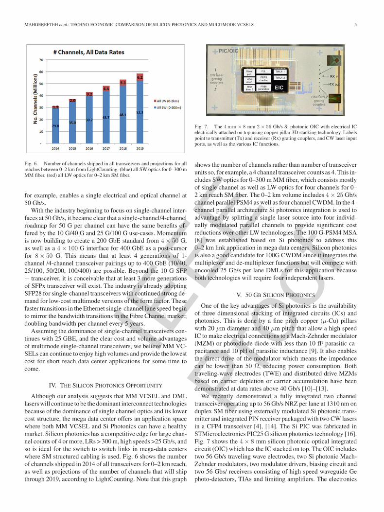
Although our analysis suggests that MM VCSEL and DMLlasers will continue to be the dominant interconnect technologiesbecause of the dominance of single channel optics and its lowercost structure, the mega data center offers an application spacewhere both MM VCSEL and Si Photonics can have a healthymarket. Silicon photonics has a competitive edge for large chan-nel counts of 4 or more, LRs > 300 m, high speeds >25 Gb/s, andso is ideal for the switch to switch links in mega-data centerswhere SM structured cabling is used. Fig. 6 shows the numberof channels shipped in 2014 of all transceivers for 0–2 km reach,as well as projections of the number of channels that will shipthrough 2019, according to LightCounting. Note that this graph
Fig. 7. The 4 mm × 8 mm 2 × 56 Gb/s Si photonic OIC with electrical ICelectrically attached on top using copper pillar 3D stacking technology. Labelspoint to transmitter (Tx) and receiver (Rx) grating couplers, and CW laser inputports, as well as the various IC functions.
shows the number of channels rather than number of transceiverunits so, for example, a 4 channel transceiver counts as 4. This in-cludes SW optics for 0–300 m MM fiber, which consists mostlyof single channel as well as LW optics for four channels for 0–2 km reach SM fiber. The 0–2 km volume includes 4 × 25 Gb/schannel parallel PSM4 as well as four channel CWDM. In the 4-channel parallel architecture Si photonics integration is used toadvantage by splitting a single laser source into four individ-ually modulated parallel channels to provide significant costreductions over other LW technologies. The 100 G-PSM4 MSA[8] was established based on Si photonics to address this0–2 km link application in mega data centers. Silicon photonicsis also a good candidate for 100G CWDM since it integrates themultiplexer and de-multiplexer functions but will compete withuncooled 25 Gb/s per lane DMLs for this application becauseboth technologies will require four independent lasers.
V. 50 GB SILICON PHOTONICS
One of the key advantages of Si photonics is the availabilityof three dimensional stacking of integrated circuits (ICs) andphotonics. This is done by a fine pitch copper (μ-Cu) pillarswith 20 μm diameter and 40 μm pitch that allow a high speedIC to make electrical connections to a Mach-Zehnder modulator(MZM) or photodiode diode with less than 10 fF parasitic ca-pacitance and 10 pH of parasitic inductance [9]. It also enablesthe direct drive of the modulator which means the impedancecan be lower than 50 Ω, reducing power consumption. Bothtraveling-wave electrodes (TWE) and distributed drive MZMsbased on carrier depletion or carrier accumulation have beendemonstrated at data rates above 40 Gb/s [10]–[13].
We recently demonstrated a fully integrated two channeltransceiver operating up to 56 Gb/s NRZ per lane at 1310 nm onduplex SM fiber using externally modulated Si photonic trans-mitter and integrated PIN receiver packaged with two CW lasersin a CFP4 transceiver [4], [14]. The Si PIC was fabricated inSTMicroelectronics PIC25 G silicon photonics technology [16].Fig. 7 shows the 4 × 8 mm silicon photonic optical integratedcircuit (OIC) which has the IC stacked on top. The OIC includestwo 56 Gb/s traveling wave electrodes, two Si photonic Mach-Zehnder modulators, two modulator drivers, biasing circuit andtwo 56 Gbs/ receivers consisting of high speed waveguide Gephoto-detectors, TIAs and limiting amplifiers. The electronics
IEEE
Proo
f
6 JOURNAL OF LIGHTWAVE TECHNOLOGY
Fig. 8. 51 Gb/s, PRBS9 optical transmitter eye diagram for Si photonic OICwith 3D stacked electrical integrated circuit at π/2 bias (a) Measurement, (b)Simulation.
integrated circuit (EIC) also provides built-in PRBS 29–1 gener-ator and checker up to 60 Gb/s, which facilitates complete errorcounting without the need for a high speed bit error rate tester orhigh speed electrodes. The EIC was implemented in a 0.13 μmSiGe BiCMOS technology using n-p-n transistors with ft andfmax both exceeding 200 GHz and 1.6 V BVCEO respectively.
Optical signals from fiber and DFB lasers are vertically cou-pled to the PIC via grating couplers [15]. Two types of gratingsare used. 1D single polarization grating couplers (SPGCs) areused on the transmitter’s outputs and CW laser input. 2D Polar-ization splitting grating couplers (PSGCs) are used on the re-ceiver inputs. SPGC have approximately 2dB insertion loss and20 nm 1 dB bandwidth around the 1310 nm peak wavelength.PSGC have approximately 4 dB insertion loss and 20 nm 1 dBbandwidth around the 1310 nm peak wavelength. Measured po-larization dependent loss is below 0.5 dB with the fiber arrayproperly aligned to the grating array.
The p-n junction high speed phase modulator used in theMZM operates based on carrier depletion and exhibits a10.5°/mm phase shift under 2.5 V bias, equivalent to Vπ·L =4.3 V·cm, and has a low insertion loss �_optical of 0.42 dB/mm.In order to achieve maximum electro-optical bandwidth, the ve-locities of the electrical driving signal and optical wave arematched by periodically loading transmission line electrodeswith p-n carrier depletion phase modulator sections [15].
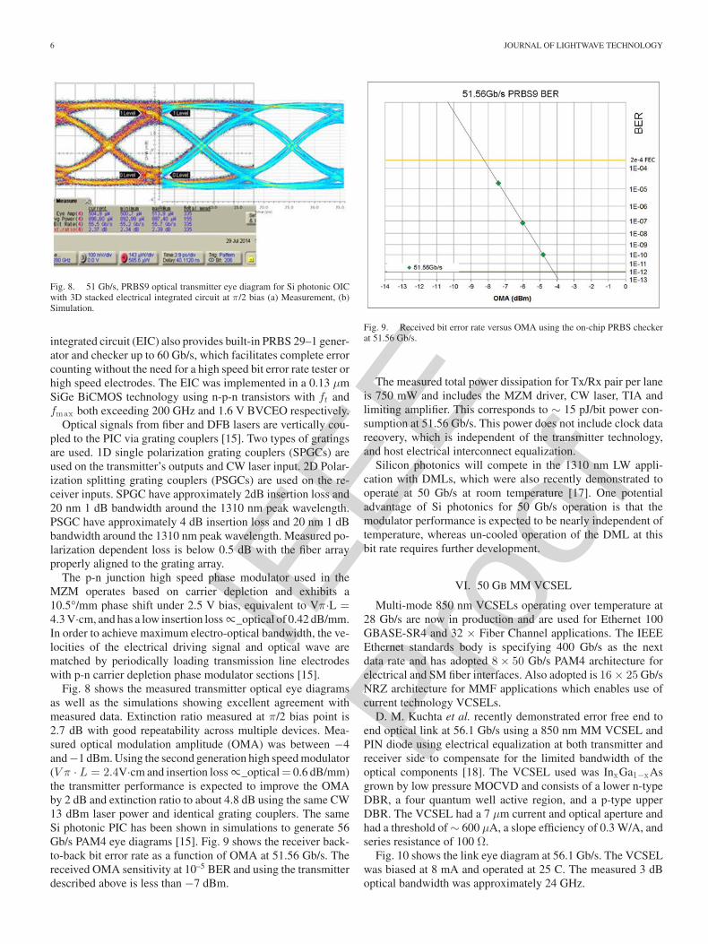
Fig. 8 shows the measured transmitter optical eye diagramsas well as the simulations showing excellent agreement withmeasured data. Extinction ratio measured at π/2 bias point is2.7 dB with good repeatability across multiple devices. Mea-sured optical modulation amplitude (OMA) was between −4and−1 dBm. Using the second generation high speed modulator(V π · L = 2.4V·cm and insertion loss �_optical = 0.6 dB/mm)the transmitter performance is expected to improve the OMAby 2 dB and extinction ratio to about 4.8 dB using the same CW13 dBm laser power and identical grating couplers. The sameSi photonic PIC has been shown in simulations to generate 56Gb/s PAM4 eye diagrams [15]. Fig. 9 shows the receiver back-to-back bit error rate as a function of OMA at 51.56 Gb/s. Thereceived OMA sensitivity at 10–5 BER and using the transmitterdescribed above is less than −7 dBm.
Fig. 9. Received bit error rate versus OMA using the on-chip PRBS checkerat 51.56 Gb/s.
The measured total power dissipation for Tx/Rx pair per laneis 750 mW and includes the MZM driver, CW laser, TIA andlimiting amplifier. This corresponds to ∼ 15 pJ/bit power con-sumption at 51.56 Gb/s. This power does not include clock datarecovery, which is independent of the transmitter technology,and host electrical interconnect equalization.
Silicon photonics will compete in the 1310 nm LW appli-cation with DMLs, which were also recently demonstrated tooperate at 50 Gb/s at room temperature [17]. One potentialadvantage of Si photonics for 50 Gb/s operation is that themodulator performance is expected to be nearly independent oftemperature, whereas un-cooled operation of the DML at thisbit rate requires further development.
VI. 50 GB MM VCSEL
Multi-mode 850 nm VCSELs operating over temperature at28 Gb/s are now in production and are used for Ethernet 100GBASE-SR4 and 32 × Fiber Channel applications. The IEEEEthernet standards body is specifying 400 Gb/s as the nextdata rate and has adopted 8 × 50 Gb/s PAM4 architecture forelectrical and SM fiber interfaces. Also adopted is 16 × 25 Gb/sNRZ architecture for MMF applications which enables use ofcurrent technology VCSELs.
D. M. Kuchta et al. recently demonstrated error free end toend optical link at 56.1 Gb/s using a 850 nm MM VCSEL andPIN diode using electrical equalization at both transmitter andreceiver side to compensate for the limited bandwidth of theoptical components [18]. The VCSEL used was InxGa1−xAsgrown by low pressure MOCVD and consists of a lower n-typeDBR, a four quantum well active region, and a p-type upperDBR. The VCSEL had a 7 μm current and optical aperture andhad a threshold of ∼ 600 μA, a slope efficiency of 0.3 W/A, andseries resistance of 100 Ω.
Fig. 10 shows the link eye diagram at 56.1 Gb/s. The VCSELwas biased at 8 mA and operated at 25 C. The measured 3 dBoptical bandwidth was approximately 24 GHz.
IEEE
Proo
f
MAHGEREFTEH et al.: TECHNO-ECONOMIC COMPARISON OF SILICON PHOTONICS AND MULTIMODE VCSELS 7
Fig. 10. Back-to-back link eye diagram for equalized MM VCSEL and pin at56.1 Gb/s. Error free (< 10–12 BER) was obtained.
The photodiode had a 25 μm active diameter and a 3 dB elec-trical bandwidth of 22 GHz at –3V. The driver included a two tapfeed forward equalizer (FFE). The receiver IC also had a two tapFFE equalizer. Both were fabricated in the IBM BiCMOS8HPprocess. Error free (BER < 10–12) operation was obtained at56.1 Gb/s for PRBS7 pattern. The power consumption for thelink, which consisted of 5 m of OM2 fiber, was 23.5 pJ/bit at56.1 Gb/s, which includes 13.4 pJ/bit for transmitter and 10pJ/bit for the receiver.
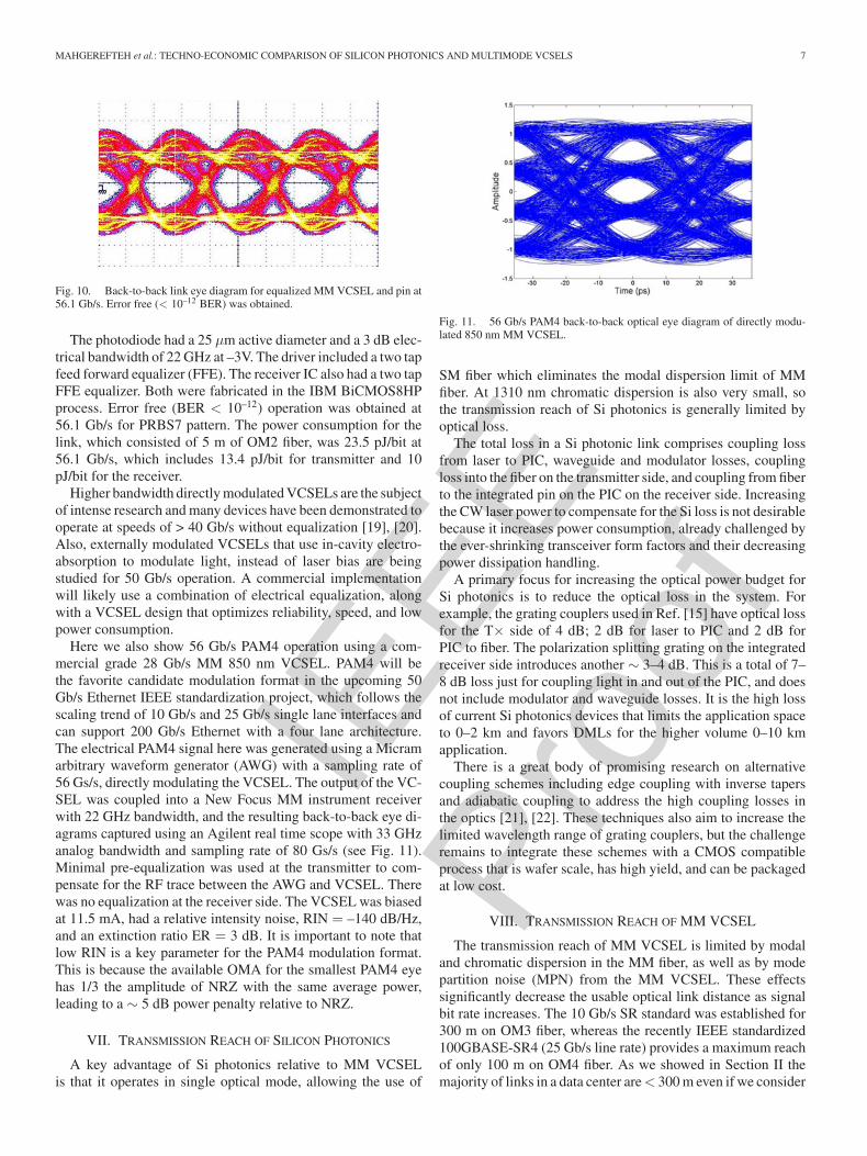
Higher bandwidth directly modulated VCSELs are the subjectof intense research and many devices have been demonstrated tooperate at speeds of > 40 Gb/s without equalization [19], [20].Also, externally modulated VCSELs that use in-cavity electro-absorption to modulate light, instead of laser bias are beingstudied for 50 Gb/s operation. A commercial implementationwill likely use a combination of electrical equalization, alongwith a VCSEL design that optimizes reliability, speed, and lowpower consumption.
Here we also show 56 Gb/s PAM4 operation using a com-mercial grade 28 Gb/s MM 850 nm VCSEL. PAM4 will bethe favorite candidate modulation format in the upcoming 50Gb/s Ethernet IEEE standardization project, which follows thescaling trend of 10 Gb/s and 25 Gb/s single lane interfaces andcan support 200 Gb/s Ethernet with a four lane architecture.The electrical PAM4 signal here was generated using a Micramarbitrary waveform generator (AWG) with a sampling rate of56 Gs/s, directly modulating the VCSEL. The output of the VC-SEL was coupled into a New Focus MM instrument receiverwith 22 GHz bandwidth, and the resulting back-to-back eye di-agrams captured using an Agilent real time scope with 33 GHzanalog bandwidth and sampling rate of 80 Gs/s (see Fig. 11).Minimal pre-equalization was used at the transmitter to com-pensate for the RF trace between the AWG and VCSEL. Therewas no equalization at the receiver side. The VCSEL was biasedat 11.5 mA, had a relative intensity noise, RIN = –140 dB/Hz,and an extinction ratio ER = 3 dB. It is important to note thatlow RIN is a key parameter for the PAM4 modulation format.This is because the available OMA for the smallest PAM4 eyehas 1/3 the amplitude of NRZ with the same average power,leading to a ∼ 5 dB power penalty relative to NRZ.
VII. TRANSMISSION REACH OF SILICON PHOTONICS
A key advantage of Si photonics relative to MM VCSELis that it operates in single optical mode, allowing the use of
Fig. 11. 56 Gb/s PAM4 back-to-back optical eye diagram of directly modu-lated 850 nm MM VCSEL.
SM fiber which eliminates the modal dispersion limit of MMfiber. At 1310 nm chromatic dispersion is also very small, sothe transmission reach of Si photonics is generally limited byoptical loss.
The total loss in a Si photonic link comprises coupling lossfrom laser to PIC, waveguide and modulator losses, couplingloss into the fiber on the transmitter side, and coupling from fiberto the integrated pin on the PIC on the receiver side. Increasingthe CW laser power to compensate for the Si loss is not desirablebecause it increases power consumption, already challenged bythe ever-shrinking transceiver form factors and their decreasingpower dissipation handling.
A primary focus for increasing the optical power budget forSi photonics is to reduce the optical loss in the system. Forexample, the grating couplers used in Ref. [15] have optical lossfor the T× side of 4 dB; 2 dB for laser to PIC and 2 dB forPIC to fiber. The polarization splitting grating on the integratedreceiver side introduces another ∼ 3–4 dB. This is a total of 7–8 dB loss just for coupling light in and out of the PIC, and doesnot include modulator and waveguide losses. It is the high lossof current Si photonics devices that limits the application spaceto 0–2 km and favors DMLs for the higher volume 0–10 kmapplication.
There is a great body of promising research on alternativecoupling schemes including edge coupling with inverse tapersand adiabatic coupling to address the high coupling losses inthe optics [21], [22]. These techniques also aim to increase thelimited wavelength range of grating couplers, but the challengeremains to integrate these schemes with a CMOS compatibleprocess that is wafer scale, has high yield, and can be packagedat low cost.
VIII. TRANSMISSION REACH OF MM VCSEL
The transmission reach of MM VCSEL is limited by modaland chromatic dispersion in the MM fiber, as well as by modepartition noise (MPN) from the MM VCSEL. These effectssignificantly decrease the usable optical link distance as signalbit rate increases. The 10 Gb/s SR standard was established for300 m on OM3 fiber, whereas the recently IEEE standardized100GBASE-SR4 (25 Gb/s line rate) provides a maximum reachof only 100 m on OM4 fiber. As we showed in Section II themajority of links in a data center are < 300 m even if we consider
IEEE
Proo
f
8 JOURNAL OF LIGHTWAVE TECHNOLOGY
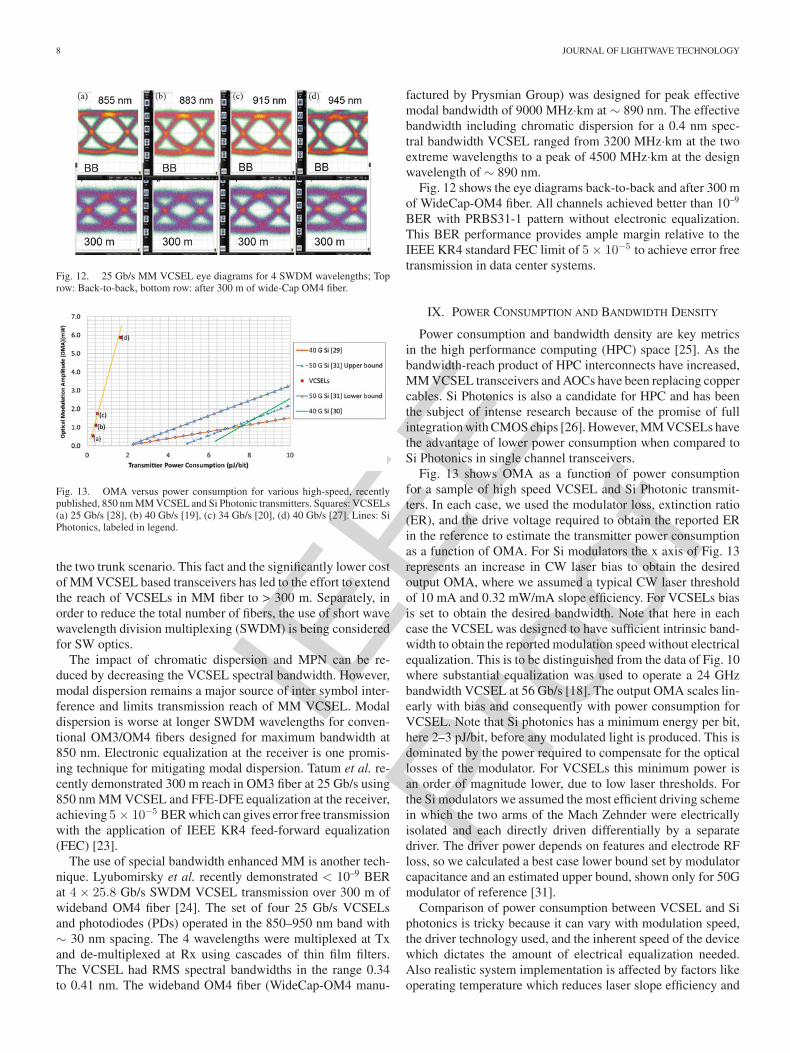
Fig. 12. 25 Gb/s MM VCSEL eye diagrams for 4 SWDM wavelengths; Toprow: Back-to-back, bottom row: after 300 m of wide-Cap OM4 fiber.
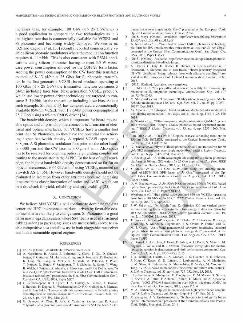
Fig. 13. OMA versus power consumption for various high-speed, recentlypublished, 850 nm MM VCSEL and Si Photonic transmitters. Squares: VCSELs(a) 25 Gb/s [28], (b) 40 Gb/s [19], (c) 34 Gb/s [20], (d) 40 Gb/s [27]. Lines: SiPhotonics, labeled in legend.
the two trunk scenario. This fact and the significantly lower costof MM VCSEL based transceivers has led to the effort to extendthe reach of VCSELs in MM fiber to > 300 m. Separately, inorder to reduce the total number of fibers, the use of short wavewavelength division multiplexing (SWDM) is being consideredfor SW optics.
The impact of chromatic dispersion and MPN can be re-duced by decreasing the VCSEL spectral bandwidth. However,modal dispersion remains a major source of inter symbol inter-ference and limits transmission reach of MM VCSEL. Modaldispersion is worse at longer SWDM wavelengths for conven-tional OM3/OM4 fibers designed for maximum bandwidth at850 nm. Electronic equalization at the receiver is one promis-ing technique for mitigating modal dispersion. Tatum et al. re-cently demonstrated 300 m reach in OM3 fiber at 25 Gb/s using850 nm MM VCSEL and FFE-DFE equalization at the receiver,achieving 5 × 10⁻⁵ BER which can gives error free transmissionwith the application of IEEE KR4 feed-forward equalization(FEC) [23].
The use of special bandwidth enhanced MM is another tech-nique. Lyubomirsky et al. recently demonstrated < 10–9 BERat 4 × 25.8 Gb/s SWDM VCSEL transmission over 300 m ofwideband OM4 fiber [24]. The set of four 25 Gb/s VCSELsand photodiodes (PDs) operated in the 850–950 nm band with∼ 30 nm spacing. The 4 wavelengths were multiplexed at Txand de-multiplexed at Rx using cascades of thin film filters.The VCSEL had RMS spectral bandwidths in the range 0.34to 0.41 nm. The wideband OM4 fiber (WideCap-OM4 manu-
factured by Prysmian Group) was designed for peak effectivemodal bandwidth of 9000 MHz·km at ∼ 890 nm. The effectivebandwidth including chromatic dispersion for a 0.4 nm spec-tral bandwidth VCSEL ranged from 3200 MHz·km at the twoextreme wavelengths to a peak of 4500 MHz·km at the designwavelength of ∼ 890 nm.
Fig. 12 shows the eye diagrams back-to-back and after 300 mof WideCap-OM4 fiber. All channels achieved better than 10–9
BER with PRBS31-1 pattern without electronic equalization.This BER performance provides ample margin relative to theIEEE KR4 standard FEC limit of 5 × 10⁻⁵ to achieve error freetransmission in data center systems.
IX. POWER CONSUMPTION AND BANDWIDTH DENSITY
Power consumption and bandwidth density are key metricsin the high performance computing (HPC) space [25]. As thebandwidth-reach product of HPC interconnects have increased,MM VCSEL transceivers and AOCs have been replacing coppercables. Si Photonics is also a candidate for HPC and has beenthe subject of intense research because of the promise of fullintegration with CMOS chips [26]. However, MM VCSELs havethe advantage of lower power consumption when compared toSi Photonics in single channel transceivers.
Fig. 13 shows OMA as a function of power consumptionfor a sample of high speed VCSEL and Si Photonic transmit-ters. In each case, we used the modulator loss, extinction ratio(ER), and the drive voltage required to obtain the reported ERin the reference to estimate the transmitter power consumptionas a function of OMA. For Si modulators the x axis of Fig. 13represents an increase in CW laser bias to obtain the desiredoutput OMA, where we assumed a typical CW laser thresholdof 10 mA and 0.32 mW/mA slope efficiency. For VCSELs biasis set to obtain the desired bandwidth. Note that here in eachcase the VCSEL was designed to have sufficient intrinsic band-width to obtain the reported modulation speed without electricalequalization. This is to be distinguished from the data of Fig. 10where substantial equalization was used to operate a 24 GHzbandwidth VCSEL at 56 Gb/s [18]. The output OMA scales lin-early with bias and consequently with power consumption forVCSEL. Note that Si photonics has a minimum energy per bit,here 2–3 pJ/bit, before any modulated light is produced. This isdominated by the power required to compensate for the opticallosses of the modulator. For VCSELs this minimum power isan order of magnitude lower, due to low laser thresholds. Forthe Si modulators we assumed the most efficient driving schemein which the two arms of the Mach Zehnder were electricallyisolated and each directly driven differentially by a separatedriver. The driver power depends on features and electrode RFloss, so we calculated a best case lower bound set by modulatorcapacitance and an estimated upper bound, shown only for 50Gmodulator of reference [31].
Comparison of power consumption between VCSEL and Siphotonics is tricky because it can vary with modulation speed,the driver technology used, and the inherent speed of the devicewhich dictates the amount of electrical equalization needed.Also realistic system implementation is affected by factors likeoperating temperature which reduces laser slope efficiency and
IEEE
Proo
f
MAHGEREFTEH et al.: TECHNO-ECONOMIC COMPARISON OF SILICON PHOTONICS AND MULTIMODE VCSELS 9
increases bias, for example. 100 Gb/s (4 × 25 Gb/s/lane) isa good application to compare the two technologies as it isthe highest rate that is commercially available for VCSEL andSi photonics and becoming widely deployed. Webster et al.[32] and Cignoli et al. [33] recently reported commercially vi-able silicon photonic modulators where the modulation functionrequires 6–11 pJ/bit. This is also consistent with PSM4 appli-cations using silicon photonics having to meet 3.5 W worst-case power consumption allowed for the QSFP28 form factor.Adding the power consumption of the CW laser this translatesto total of 8–13 pJ/bit at 25 Gb/s for Si photonic transmit-ter. In the first generation VCSEL-based products operating at100 Gb/s (4 × 25 Gb/s) the transmitter function consumes 5pJ/bit including laser bias. Next generation VCSEL products,which use lower power driver technology are targeted to con-sume 2–3 pJ/bit for the transmitter including laser bias. As onesuch example, Shibata et al. has demonstrated a commerciallyavailable 850-nm VCSEL with 1.8 pJ/bit power consumption at25.7 Gb/s using a 65-nm CMOS driver [34].
The bandwidth density, which is important for board mount-able optics and chip-to-chip interconnects, is a function of elec-trical and optical interfaces, but VCSELs have a smaller footprint than Si Photonics, so they have the potential for achiev-ing higher bandwidth density. A typical VCSEL aperture is∼ 8 μm. A Si photonics modulator foot print, on the other hand,is ∼300 μm and the CW laser is 300 μm–1 mm. Also spacehas to be reserved for coupling optics; e.g., grating coupler androuting to the modulator in the Si PIC. To the best of our knowl-edge, the highest bandwidth density demonstrated so far for anoptical interconnect is 64 Gb/s/mm2 using VCSEL mounted ona switch ASIC [35]. However bandwidth density should not beevaluated in isolation from other attributes because increasingit necessitates closer integration of optics and ASIC, which canbe a drawback for yield, reliability and serviceability [25].
X. CONCLUSION
We believe MM VCSELs will continue to dominate the datacenter and HPC interconnect markets, driven by favorable eco-nomics that are unlikely to change soon. Si Photonics is a goodfit for new mega data centers where SM fiber is used in structuredcabling as long as packaging issues are successfully solved to en-able competitive cost and allow use in both pluggable transceiverand board mountable optical engines.
REFERENCES
[1] (2015). [Online]. Available: http://www.molex.com.[2] A. Narasimha, B. Analui, E. Balmater, A. Clark, T. Gal, D. Gucken-
berger, S. Gutierrez, M. Harrison, R. Ingram, R. Koumans, D. Kucharski,K. Leap, Yi. Liang, A. Mekis, S. Mirsaidi, M. Peterson, T. Pham,T. Pinguet, D. Rines, V. Sadagopan, T. J. Sleboda, D. Song, Y. Wang,B. Welch, J. Witzens, S. Abdalla, S. Gloeckner, and P. De Dobbelaere, “A40-Gb/s QSFP optoelectronic transceiver in a 0.13 μm CMOS silicon-on-insulator technology,” presented at the Opt. Fiber Communications Conf.,Carlsbad, CA, USA, 2008, Paper MK7.
[3] C. Sciancalepore, R. J. Lycett, J. A. Dallery, S. Pauliac, K. Hassan,J. Harduin, H. Duprez, U. Weidenmueller, D. F. G. Gallagher, S. Menezo,and B. Ben Bakir, “Low-crosstalk fabrication-insensitive Echelle gratingdemultiplexers on silicon-on-insulator,” IEEE Photon. Technol. Lett., vol.27, no. 5, pp. 494–497, Mar. 2015.
[4] G. Denoyer, A. Chen, B. Park, Z. Yuxin, A. Santipo, and R. Russo,“Hybrid silicon photonic circuits and transceiver for 56 Gb/s NRZ 2.2 km
transmission over single mode fiber,” presented at the European Conf.Optical Communication, Cannes, France, 2014.
[5] (2015, May). [Online]. Available: http://www.ieee802.org/3/bs/public/15_05/welch_3bs_01a_0515.pdf
[6] A. Narasimha et al., “An ultralow power CMOS photonics technologyplatform for H/S optoelectronics transceivers at less than $1 per Gbps,”presented at the Optical Fiber Communications Conf., San Diego, CA,USA, 2010, Paper OMV4.
[7] (2015). [Online]. Available: http://www.macom.com/products/photonic-solutions/distributed-feedback-lasers.
[8] A. Descos, C. Jany, D. Bordel, H. Duprez, G. Beninca-de-Farias, P.Brianceau,, S. Menezo, and B. Ben Bakir, “Heterogeneously integratedIII–V/Si distributed Bragg reflector laser with adiabatic coupling,” pre-sented at the European Conf. Optical Communication, London, U.K.,2013.
[9] (2015). [Online]. Available: www.psm4.org[10] S. Joblot et al., “Copper pillar interconnect capability for mmwave ap-
plications in 3D integration technology,” Microelectron. Eng., vol. 107pp. 72–79, 2013.
[11] M. Streshinsky et al., “Low power 50 Gb/s silicon traveling wave Mach-Zehnder modulator near 1300 nm,” Opt. Exp., vol. 21, no. 25, pp. 30350–30357, Dec 2013.
[12] Xi. Xiao et al., “High-speed, low-loss silicon Mach–Zehnder modulatorswith doping optimization,” Opt. Exp., vol. 21, no. 4, pp. 4116–4125, Feb2013.
[13] A. Shastri et al., “Ultra-low-power single-polarization QAM-16 gener-ation without DAC using a CMOS photonics based segmented modu-lator,” IEEE J. Lightw. Technol., vol. 33, no. 6, pp. 1255–1260, Mar.2015.
[14] Ran. Ding et al., “100-Gb/s NRZ optical transceiver analog front-end in130-nm SiGe BiCMOS,” presented at the Optical Interconnects Conf.,San Diego, CA, USA, 2014.
[15] G. Denoyer et al., “Hybrid silicon photonic circuits and transceiver for 50gb/s NRZ transmission over single-mode fiber,” IEEE J. Lightw. Technol.,vol. 33, no. 6, pp. 1247–1254, Mar 2015.
[16] F. Boeuf et al., “A multi-wavelength 3D-compatible silicon photonicsplatform on 300 mm SOI wafers for 25 Gb/s applications,” in Proc. IEEEInt. Electron. Devices Meet., 2013, pp. 13.3.1–13.3.4.
[17] Y. Matsui et al. “112 Gb/s WDM link using two directly modu-lated Al-MQW BH DFB lasers at 56 Gb/s,” presented at the Op-tical Fiber Communications Conf., Los Angeles, CA, USA, 2015,Paper Th5B6.
[18] D. M. Kuchta et al., “A 56.1Gb/s NRZ modulated 850nm VCSEL-basedoptical link,” presented at the Optical Fiber Communications Conf., Ana-heim, CA, USA, 2013, Paper OW1B5.
[19] Westberg et al., “High-speed oxide confined 850 nm VCSELs operatingerror free at 40 Gb/s up to 85 C,” IEEE Photon. Technol. Lett., vol. 25,no. 8, pp. 768–771, Apr. 2013.
[20] J.-W. Shi et al., “Oxide-relief and Zn-diffusion 850 nm vertical cavitysurface emitting lasers with extremely low energy to data rate ratios for40 Gb/s operations,” IEEE J. Sel. Topics Quantum Electron., vol. 19,no. 2, p. 7900208, Mar./Apr. 2013.
[21] T. Barwicz, A. Janta-Polczynski, M. Khater, Y. Thibodeau, R. Leidy,J. Maling, S. Martel, S. Engelmann, J. S. Orcutt, P. Fortier, and W.M. J. Green, “An o-band metamaterial converter interfacing standardoptical fibers to silicon nanophotonic waveguides,” presented at theOptical Fiber Communication Conf., Los Angeles, CA, USA, 2015,Paper Th3F3.
[22] R. Dangel, J. Hofrichter, F. Horst, D. Jubin, A. La Porta, N. Meier, I. M.Soganci, J. Weiss, and B. J. Offrein, “Polymer waveguides for electro-optical integration in data centers and high-performance computers,” Opt.Exp., vol. 23, no. 4, pp. 4736–4750, 2015.
[23] J. A. Tatum, D. Gazula, L. A. Graham, J. K. Guenter, R. H. Johnson,J. King, C. Kocot, G. D. Landry, I. Lyubomirsky, A. N. MacInnes,E. M. Shaw, K. Balemarthy, R. Shubochkin, D. Vaidya, M. Yan, and F.Tang, “VCSEL-based interconnects for current and future data centers,”J. Lightw. Technol., vol. 33, no. 4, pp. 727–732, Feb. 15, 2015.
[24] I. Lyubomirsky, R. Motaghian, H. Daghighian, D. McMahon, S. Nelson,C. Kocot, J. A. Tatum, F. Achten, P. Sillard, D. Molin, and A. Amezcua-Correa, “100G SWDM4 transmission over 300 m wideband MMF,” inProc. Eur. Conf. Opt. Commun., 2015, paper P. 5. 4.
[25] M. A. Taubenblatt, “Optical interconnects for high performance comput-ing,” J. Lightw. Technol., vol. 30, no. 4, pp. 448–457, Feb. 2012.
[26] X. Zheng and A. V. Krishnamoorthy, “Si photonics technology for futureoptical interconnection,” presented at the Communications and Photon.Conf. Exhib., Shanghai, China, 2011.
IEEE
Proo
f
10 JOURNAL OF LIGHTWAVE TECHNOLOGY
[27] P. Wolf, P. Moser, G. Larisch, H. Li, J. A. Lott, and D. Bimberg, “En-ergy efficient 40 Gb/s transmission with 850 nm VCSELs at 108 fJ/bitdissipated heat,” Electron. Lett., vol. 49, no. 10, pp. 666–667, 2013.
[28] P. Moser, J. A. Lott, D. Bimberg, “Energy efficiency of directly modulatedoxide-confined high bit rate 850 nm VCSELs for optical interconnect,”IEEE J. Sel. Topics Quantum Electron., vol. 19, no. 4 p. 1702212, Jul./Aug.2013.
[29] D. J. Thomson et al., “High contrast 40 Gbit/s optical modulation insilicon,” Opt. Exp., vol. 19, no. 12, pp. 11507–11516, 2011.
[30] P. Dong et al., “High-speed low-voltage single-drive push-pull siliconMach-Zehnder modulators,” Opt. Exp., vol. 20, pp. 6163–6169, 2012.
[31] X. Xiao et al., “High-speed, low-loss silicon Mach–Zehnder modulatorswith doping optimization,” Opt. Exp., vol. 21, pp. 4116–4125, 2013.
[32] M. Webster et al., “Silicon photonic modulator based on a MOS-capacitorand a CMOS driver,” presented at the Compound Semicond. IntegratedCircuit Symp., La Jolla, CA, USA, 2015, paper Session E.
[33] M. Cignoli et al., “A 1310-nm 3-D integrated silicon photonics Mach–Zehnder-based modulator transmitter with 275 mW multi-stage CMOSdriver achieving 6dB extinction ratio at 25Gb/s,” in Proc. IEEE Int. SolidState Circ. Conf., 2015, Session 22.9.
[34] M. Shibata et al., “26Gb/s 1.8-pJ/bit CMOS-driven transmitter for 850-nm common cathode VCSELs,” presented at the Optical Fiber Conf., LosAngles, CA, USA, 2015, Paper OTu3G.1.
[35] K. Hasharoni et al., “A high end routing platform for core and edgeapplications based on chip to chip optical interconnect,” presented at theOpt. Fiber Conf., Anaheim, CA, USA, 2013, Paper OTu3H.2.
Daniel Mahgerefteh was born in Isfahan, Iran, in 1963. He received the Ph.D.degree in physics from the University of Southern California, Los Angeles, CA,USA, in 1990. He was a Research Faculty with the Laboratory for Physical Sci-ences, University of Maryland from 1993 to 2000. He is currently the director ofthe advanced technology at Finisar Corporation, Sunnyvale, CA, USA, workingon integrated photonics and low cost packaging technologies for data commu-nications market. He was the Cofounder and Chief Technology Officer of AznaLLC and the coinventor of the Chirp Managed Laser technology. He has morethan 50 issued or pending patents and is the author of numerous publications.
Craig Thompson received the Bachelor of Engineering (Hons.) degree from theUniversity of New South Wales, Sydney, N.S.W, Australia, and the MBA degreefrom the Massachusetts Institute of Technology, Cambridge, MA, USA. He iscurrently the Director of Strategic Marketing at Finisar Corporation, Sunnyvale,CA, USA. His research interests include long-term product and technologyroadmaps for optical communications, and contributes to advanced developmentactivities supporting the roadmaps. He has held a number of marketing andproduct management roles in optical communications, networking, and storagein companies such as Intel, Gennum, and EMC, spanning 15 years.
Chris Cole received the B.S. degree in aeronautics and astronautics, and the B.S.and M.S. degrees in electrical engineering, all from the Massachusetts Instituteof Technology, Cambridge, MA, USA. He is currently the Director at FinisarCorporation, Sunnyvale, CA, USA, where he is architecting and leading the de-velopment of 50-, 100-, 200-, and 400-Gb/s optical interfaces and transceivers.At Hughes Aircraft Co. (currently Boeing SDC) and then the M.I.T. LincolnLaboratory, he contributed to multiple imaging and communication satelliteprograms such as Milstar. He later consulted on telecom ASIC architecturesand designs for Texas Instruments DSP Group and Silicon Systems, Inc. (cur-rently Maxim.). He was one of the architects of the Sequoia coherent imagingultrasound platform at Acuson Corp. (currently Siemens Ultrasound), where healso managed hardware and software groups. As a Principal Consultant with theParallax Group he carried out signal processing analysis and product definitionfor several imaging and communication systems. At BBN, a Finisar acquisition,he developed 10 Gb/s and 40 Gb/s optical transceivers.
Gilles Denoyer (M’02) received the M.S. degree from Supelec EngineeringSchool, Gif Sur Yvette, France, in 1995. In 1996, he was with SGS-ThomsonMicroelectronics (STMicroelectronics since 1998), San Jose, CA, USA, and wasinvolved with the design of MR preamplifiers for hard disk drives. In 2002, hewas with Finisar Corporation, Sunnyvale, CA, where he worked on the design oftransimpedance amplifiers, CDRs, and 100G Gearbox ICs. His current researchinterests include silicon photonics and high-speed circuits for next generationfiber optics transceivers.
Thelinh Nguyen received the Bachelor’s of Engineering and Master.s of Engi-neering degrees from the University of Waterloo, Waterloo, ON, Canada, andQueen’s University, Kingston, ON, Canada, respectively. He is currently theDirector of IC Engineering at Finisar Corporation, Sunnyvale, CA, USA. Heworks on optical front-ends and retiming circuits for 100G and 400G opticaltransceiver products. Since 1999, he has been with Finisar Corporation. Prior toFinisar, he spent seven years with Nortel Networks developing IC’s and modulesfor OC-192 and OC-768 applications.
Ilya Lyubomirsky received the Ph.D. degree in electrical engineering fromMassachusetts Institute of Technology, Cambridge, MA, USA, in 1999. Early inhis career at Telcordia and ONI Systems Inc., he contributed to system modelingand design of high-speed packet and optical metro networks. He developedultradense WDM transmission systems at Ciena Corporation, and involved inthe research of PIC-based fiber-optic communications at Infinera Corporation.From 2003 to 2010, he was an electrical engineering Faculty at University ofCalifornia, Riverside. He is currently at the Finisar Corporation, Sunnyvale, CA,USA, involved in research work of advanced modulation, DSP algorithms, andcoding techniques to enable advanced optical modules for 100/400 Gb/s, etc.He has coauthored about 50 peer-reviewed journals, conference papers, and tenpatents.
Chris Kocot received the Ph.D. degree in electrical engineering under an ex-change program between Warsaw University, Warszawa, Poland, and StanfordUniversity, Stanford, CA, USA. He is the Director at Finisar Corporation, Sun-nyvale, CA, where he provides technical leadership to R & D projects in the areaof high-speed module design, microwave and signal-integrity simulations, andoptics design. He is also working on high-speed VCSEL development projects.He was with the Hewltt-Packard Laboratories, Palo Alto, CA, as a Member ofTechnical Staff on MESFETs and later on HEMTs and subsequently on high-speed photo-detectors, APDs, LEDs, and VCSELs. He became a Departmentmanager at the Agilent Fiber-Optics Division, San Jose, CA. His departmentdeveloped state of the art 850 and 980 nm VCSELs and high-speed photo-detectors (APDs and photo-HBT). He then joined Novalux, Inc., Sunnyvale,CA, as the Director of the Laser Engineering Group. He led the developmentof high-power red, green, and blue external-cavity lasers from their infancy tomaturity with proven reliability and high power in the visible range (3W red, 8Wgreen, and 8W blue). He has more than 20 patents related to photo-detectors,APDs, HEMTs, ICs, LEDs, and VCSELs.
Jim Tatum was born in Hayward, CA, USA, in 1967. He received the B.A.degree from Austin College, Sherman, TX, USA, in 1989, and the M.S. andPh.D. degrees from the University of Texas, Dallas, TX, in 1992 and 1995,respectively. He was with Honeywell in 1996 as a VCSEL Design Engineerafter a brief stint with the Polaroid Corporation. He is currently the Directorof VCSEL and Photodiode product development in Finisar Corporation, Allen,TX. He has been the author of more than 30 technical papers and holds morethan 30 patents.

IEEE
Proo
f
JOURNAL OF LIGHTWAVE TECHNOLOGY 1
Techno-Economic Comparison of SiliconPhotonics and Multimode VCSELs
Daniel Mahgerefteh, Craig Thompson, Chris Cole, Gilles Denoyer, Thelinh Nguyen,Ilya Lyubomirsky, Chris Kocot, and Jim Tatum
(Invited Paper)
Abstract—Recent technical and commercial milestones in SiliconPhotonics technology including its introduction into commercialfoundries, and successful integration of most optical components,as well as the choice of single mode fiber in some mega data cen-ters have prompted the speculation that Si photonics is the newlow cost solution for optical interconnects and that it may replacemulti-mode vertical cavity surface emitting lasers (MM VCSEL).We show that the dominant technology has to offer the lowest costfor the single channel transceiver application, which represents90% of the data center market and which historically dominatessales. We show that Si photonics is currently significantly more ex-pensive than MM VCSEL for single channel, but that it can makea successful entry into the four channel single mode market withsignificant growth, capturing 20% of the data center market. Wediscuss the challenges with Si/InP integration; i.e., hybrid lasers forbreaking the cost barrier and to enter the market. We show thatboth MM VCSEL and Si photonics technologies can operate at50 Gb/s. We discuss the transmission reach limitations of Si pho-tonics and MM VCSEL and show an example of reach extension for100 Gb/s using MM VCSEL to 300 m of MM fiber. In addition weshow that MM VCSEL has fundamentally lower power consump-tion than Si photonics and is a good candidate for super-computingapplications.
Index Terms—Multimode Vertical Cavity Surface EmittingLaser, data centers, hybrid lasers, Silicon Photonics.
I. INTRODUCTION
S ILICON Photonics has been in the spotlight in recent yearswith a number of technological and commercial highlights.
Active optical cables (AOCs) and “pigtailed” transceivers using4 × 10 Gb/s silicon (Si) photonic integrated circuits (PIC) havebeen in the market for a few years [1]. A number of commer-cial CMOS foundries including IBM and ST Microelectronicsare adding Si photonics into their manufacturing lines, and re-searchers have shown that most optical functions, save the laserand isolator, can be integrated in Si [2]–[4]. Some new mega-data centers are being designed with single mode (SM) fiberinfrastructure cabling, opening a market for Si photonics. Thesetechnical and commercial milestones, as well as the old adage,
Manuscript received July 8, 2015; revised August 21, 2015; accepted Septem-ber 11, 2015.
The authors are with the Finisar Corporation, Sunnyvale, CA 94089 USA(e-mail: [email protected]; [email protected]; [email protected]; [email protected]; [email protected];[email protected]; [email protected]; [email protected]).
Color versions of one or more of the figures in this paper are available onlineat http://ieeexplore.ieee.org.
Digital Object Identifier 10.1109/JLT.2015.2483587
“If you compete with CMOS, don’t!” have prompted the specu-lation that Si photonics is the new low cost solution for opticalinterconnects. Is Si photonics the future of optical interconnectsand will it replace MM VCSELs? We attempt to answer thisquestion by comparing Si photonics and MM VCSELs basedon their applicable markets, relative costs, transmission reach,power consumption, and bandwidth-density.
Cost is particularly important for data center applications be-cause optical interconnects are becoming a significant part ofthe total bill of materials. The massive parallelism imposed bythe architectures used increases the number of interconnectsbetween switches and increases the average link length whichrequire the more expensive single-mode transceivers thereby in-creasing the total cost of interconnects between them. Also theservers, memory, and electrical packet switches used in thesesystems have benefitted from high volume, mature CMOS tech-nology, which uses wafer level processes, test, and packaging, soit is assumed that optics can similarly benefit. We will examinethis premise here.
In Section II we make a comparison of the application spaceand cost structure of Si photonics and multi-mode VCSEL fordata center applications. We will show that the majority of thetransceiver volume is in single channel form, which biases thecost competition between the technologies in favor of 850 nmMM VCSEL or 1310 nm directly modulated lasers (DMLs). InSection III we explain why single channel is the dominant formfactor today and explore its future. In Section IV we show thatSi photonics has a large and growing market opportunity in thefour channel parallel (PSM4) and course wavelength divisionmultiplexing (CWDM) applications spaces which are especiallysuited to the mega data centers. In Sections V and VI we showthat both Si photonics and MM VCSEL, respectively, can oper-ate at 50 Gb/s. In Section VII we discuss limitation to the trans-mission reach of Si photonics. In Section VIII we discuss thereach limitation of MM VCSEL and present an example of reachextension to 300 m for at 100 Gb/s for. In Section IX we comparethe power consumption of high speed VCSEL and Si photonicstransmitters and show that VCSELs have fundamentally lowerpower consumption, and we conclude with Section X.
II. VOLUME AND COST
Multimode VCSELs operating on multimode fiber are dom-inating short reach links in data centers today because they arethe lowest cost. The reasons for the current cost difference be-tween Si photonics and MM VCSEL are part economics andpart technical. In this section we focus on the economic side.
0733-8724 © 2015 IEEE. Personal use is permitted, but republication/redistribution requires IEEE permission.See http://www.ieee.org/publications standards/publications/rights/index.html for more information.
IEEE
Proo
f
2 JOURNAL OF LIGHTWAVE TECHNOLOGY
Fig. 1. Application space in current data centers based on (a) transmissionreach and fiber type, (b) loss budget, or (c) technology.
Fig. 2. Distribution of OM4 MM trunk fiber cables manufactured between1/2012 and 12/2014 versus length. Line is accumulated percentage. (Courtesyof Corning Corporation).
Costs drop when volumes increase, especially when the man-ufacturing technology has a high up-front capital expenditureassociated with it (such as CMOS fabrication), so comparisonof the two technologies has to be made for the applications withthe highest volumes.
The data communication application space is currently parsedout by transmission reach and fiber type, multi-mode fiber(MMF), or SM fiber (SMF), and loss budget for the opticallink, and is currently dominated by MM VCSEL and DML tech-nologies (see Fig. 1). The loss budget and transmission reach areestablished by various communications standards such as IEEE,TIA, etc., and are based on industry consensus on available tech-nology that is expected to be manufactured at the lowest cost.Since we are trying to compare the highest volume applicationsfor cost, we will focus on the IEEE Ethernet 802.3ae. Until re-cently there were only two sets of standards: 1) The short reach(SR) standards intended for MM 850 nm VCSEL for 300 m at10 Gb/s and 100 m for 100 Gb/s and 2) The long reach (LR)standard intended for SM fiber at 1310 nm for 0–10 km and achannel insertion loss of 6.2 dB. Fig. 1 also shows a 2000 m SMfiber reach with 3–4 dB loss budget, which represents the newermega data center application and is currently being addressedthrough industry multi-source agreements (MSAs).
Despite the rapid growth of mega data centers with > 250ksquare foot area, the enterprise data centers, which are mostlyless than 25k square feet, have installed MMF. Today the ma-jority of the fiber in data centers is multi-mode fiber with OM3or OM4 varieties. Fig. 2 shows the distribution of trunk fibercables in data centers manufactured between Jan 2012 to Dec2015 by Corning Corporation and the cumulative percentage(solid line). Note that over 90% of the links are less than 100 m.
Fig. 3. Units of transceivers shipped in 2013 and projected through 2018 fromLightCounting as a function of number of channels.
Even considering the case of two patch panels with three trunkcables in a link, the majority of links in data centers are < 300 m.
Some newer mega data centers are installing SM fiber fortheir structured fiber optic cabling to accommodate the moreparallel architectures, the larger number of interconnects, andthe longer average links suited to their data processing intensiveapplications. Also as the aggregate data rate increases from 10to 100 Gb/s the reach of VCSEL in MM fiber is decreasing from300 to 100 m due to modal dispersion, which is an argument fornew installations to use SM fiber for future proofing. In additionthe mega data centers have shown a steady rapid growth ininfrastructure spending and represent a growing market thatrequires attention. SMF is in fact less expensive per unit lengththan MMF due to the tight manufacturing tolerances for thelater. So, if the SM transceiver could be made at the same costas MM transceiver, there would be good reason to switch to SMtechnology. This is the purported opportunity for Si photonicstechnology. Since low cost is, in large part, dependent on highvolumes, can Si photonics replace MM VCSEL if data centerswould all switch to SM fiber?
To answer this question, let us consider a hypothetical sce-nario where we replace all MMF in all data centers with SMF.In addition let us consolidate all SR, LR standards and the 2 kmMSA into one standard and assume that Si photonics can meetall loss budgets including the 0–10 km. In this case the potentialvolume for Si photonics would be the application space for all10 Gb/s and higher bit rate transceivers regardless of trans-mission reach or type of fiber. Having thus consolidated thishypothetical application space we look at the volume of alltransceivers as a function of number of channels. Fig. 3 showsthe number of all transceivers both short wave, 850 nm (SW)and long wave, 1310 nm (LW) shipped in 2013 and the sameprojected through 2018 as reported in 2015 by LightCounting,as a function of number of channels in each module. The contrastin volumes is striking. There were over 25 million transceiversshipped in 2013, of which 96% were single channel transceivers.A single channel transceiver has a single high speed electrical in-terface input, and a single wavelength, single duplex fiber optical
IEEE
Proo
f
MAHGEREFTEH et al.: TECHNO-ECONOMIC COMPARISON OF SILICON PHOTONICS AND MULTIMODE VCSELS 3
Fig. 4. Single channel price for 10 G SFP+ for SW, which uses MM 850 nmVCSEL and LW, which uses 1310 nm InP DFBs.
output. Examples of four channel transceivers are 100 G LANWDM and PSM4 both with 4 × 25 G electrical inputs and withfour optical wavelengths or four parallel output fibers, respec-tively. The volumes in Fig. 3 include Ethernet, Fiber Channel,as well as “optical interconnects” as defined by LightCounting,which includes AOCs, high density parallel transceivers andembedded optical engines. The data does not include wirelessbackhaul and SONET/SDH volumes, which are almost entirelysingle-channel devices, but excluded from the analysis to focuson the data center opportunity.
The single channel volume dominates because, as it has beenshown for lower Ethernet data rates, once the component tech-nology is mature enough to allow the data to be transmitted usinga single channel, it becomes the lowest cost solution. Accord-ing to LightCounting, in 2014 over 65% of optical transceivervolume was SW for 0–300 m, and the remaining 35% was LWoptics for 0–10 km, which is currently dominated by DMLs. TheSW to LW ratio is expected to reduce slightly as SM becomemore important, but multimode is expect to be 60% or more ofthe volume over the next 5 years, according to LightCounting.
For Si photonics transmitters to become the dominant tech-nology over MM VCSELs and capture the volume it has to belower cost than a single channel short wave MM VCSEL. Apoint of cost comparison between short wave (SW) and LWoptics is the 10 G small form factor plus (SFP+) transceiver,which uses mature technologies; MM VCSEL for SW and InPDFB for LW, and has an established market (Fig. 4). Accordingto LightCounting the price of LW 10 G SFP+ was 2.6 timeshigher than that of 10 G SFP+ SW in 2013, with a relativelysharp drop in 2015 caused by fierce competition, and the ratiopredicted to drop to 2.2× by 2018. This > 2× cost differential ismainly due to the lower packaging cost of MM VCSEL enabledby; 1) self hermeticity of the VCSEL, which avoids a costlypackage, 2) an order of magnitude larger alignment tolerance ofMM, 3) use of plastic coupling optics, and 4) the lack of opticalisolator for MM VCSEL. Larger GaAs wafer size relative to InP,wafer level testing, and vertical construct of SW VCSEL, which
Fig. 5. Schematic diagrams of DML and Si photonic transmitter integratedcircuit for a single channel transceiver application.
naturally protects the active region, also contribute to reducingthe laser cost by increasing manufacturability and yield.
Overcoming the single channel DFB cost barrier and surpass-ing it to compete with SW MM optics is very challenging forSi Photonics. Today the Si photonics transceivers in the marketcomprise an InP CW laser and an optical isolator in a hermeticSi package, the Si PIC, which includes an external modulator,photodiode (PIN) receiver, and may further include integrateddriver and transimpedance amplifier (TIA), and optics for cou-pling light from the laser to the Si PIC and finally from thePIC to fiber [5]. This construct is clearly more complex than adirectly modulated DFB based transceiver since it still requiresa hermetic package for the laser, in addition to the Si PIC (seeFig. 5). Integration of driver and TIA is clearly beneficial butthe Si PIC does not integrate enough functions to reduce costfor a single channel.
Self-hermetic DFBs are in development [6] and can reducepackage cost for both DML and Si Photonics transceivers in thenear future. Hybrid InP/Si technology which integrates the InPgain material with a passive DBR and Si modulator, eliminatescoupling optics and tight alignment tolerances at the laser-PICinterface, and potentially eliminates a hermetic package by pro-viding a dielectric seal for the laser [7]. However, the yieldand reliability of hybrid lasers still needs to be established, andtransceiver cost yet to be tested in the market.
A major key to the success of CMOS electronics and thepromise of Si photonics is the well-controlled Si processes, ex-cellent predictability of device performance based on processdesign kits (PDKs), very high yield, and high device reliability.High circuit yield enables a large number of functions to beintegrated on a single Si chip at low cost. Monolithic InP lasers,on the other hand, are far from Si in process control, yield,and reliability. This is especially true of Aluminum containingInP 1310 lasers which are more prone to failure. This issue iscircumvented in today’s standard micro-optics packaging plat-forms by burning in individual laser die and using known gooddie in the product. This way the laser yield only affects the laserchip cost, not the entire package cost. A low yielding hybridlaser integrated with a number of other functions in a Si PICwould increase the cost of the entire PIC and hence the packagedtransceiver. In the context of cost, hybrid lasers should target thegoal to show much better burn-in yield than monolithic lasersto make the integrated hybrid platform economically viable. Inaddition, tight tolerances for coupling light into SM fiber, andoptical isolation remain differential cost adders for all SM tech-nologies relative to MM optics, and require further innovationand development to eliminate their need.
IEEE
Proo
f
4 JOURNAL OF LIGHTWAVE TECHNOLOGY
TABLE IDATA RATES FOR SWITCH AND SERVER INTERCONNECTS FROM 2.5 GB/S PER
LANE TO 25 GB/S PER LANE AND YEAR OF ADOPTION
(50 GB/S IN 2017 IS A PROJECTION)
Main streamSwitch
Main streamSwitch
IEEEEthernet
Per Lane Rate and No. of Lanes toSupport Switch Rate
SupportedServer
Rate Gb/s ASIC I/OStandard
Standard 2.5 Gb/s 10 Gb/s 20–25 Gb/s
40–50 Gb/s
Rate Gb/s
10 2002 802.3ae 4× 1× 140 2010 802.3ba 4× 2× 1× 10100 2014 802.3bj 4× 2× 25200 2017∗ n.a. 4× 50
III. THE PAST AND FUTURE OF SINGLE CHANNEL OPTICS
Single channel optics dominates the market because it is thelowest cost solution for transmitting bits from point to point us-ing mature technology. This has been the trend for many gener-ations of Ethernet, Fiber Channel, wireless CPRI, SONET/SDHand other protocols. Table I show the historical progression ofdata rate standards for mainstream switch and server intercon-nects and year of adoption. Note that the first generation ofmainstream switch ASIC I/O is 4 lanes with each lane runningat ¼ of the switch rate. However multiple lanes are replacedby a single channel as soon as the higher rate optical intercon-nect technology becomes mature and available at low cost. Forexample to support a 10 Gb/s input/output rate for a switch, 4channels of 2.5 Gb/s were initially used. However, this was re-placed by a single channel 10 Gb/s when the higher rate becamemature and could support the cost structure. At this point, thesingle channel also migrates to the server interconnect, which ismuch more cost sensitive.
The single channel application has been realized through thevariants of the small form factor pluggable transceiver; SFP for4 Gb/s and less and SFP+ for > 8 Gb/s. The SFPs have beenvery successful in the market, commanding 95% of the volumeof interfaces up to 2 km in reach, which is the realm of the datacenter, and even higher when one considers all shipments up to10 km. Of all transceivers up to 10 km, including single chan-nel, four channels or more, 65% are SW MM VCSEL basedtransceivers; two times the volume of LW SM optics. The lowercost of SW transceivers leads to higher volume which leads toan even lower cost through better yield, more suppliers, andbetter economics in the supply chain. This provides a tremen-dous inherent advantage for single channel, SW MM pluggabletransceivers.
Besides cost, the single-channel transceiver also has tremen-dous utility for the majority of the customer base, includingenterprise, telecomm, and service-providers, video broadcastand industrial customers which together represent 80% of themarket. The SFP/SFP+ transceiver module is simple to deploy,as it is just the right size for handling, and can be deployedone interface at a time. It also uses mature and reliable serialelectrical and duplex LC optical connectors and can be obtainedin many different configurations such as bit rate, transmissionreach, and other features, from many different suppliers. TheSFP/SFP+ single channel form factor also fits the deploymentpattern of this segment of the market since they tend to populate
the network interfaces at the server and switch levels one or afew interfaces at a time as demands grows.
With the advent of the mega data center, attention has beenquickly diverted away from the single-channel, pluggable opti-cal transceiver towards multi-channel transceivers that meet theunique bandwidth and I/O density demands of the hyper-scaledata center. These are either 4-channel parallel interfaces thatare used to connect top of rack switches to multiple aggregationswitches higher in the network topology, or 4-channel wave-length division multiplexed (WDM) interfaces that allow theaggregation of bandwidth for dozens or hundreds of servers at atime. These are advanced optical transceivers and are inherentlymore complex, and more costly than single-channel, multimode,pluggable transceivers. These advanced hyper-scale interfacesprovide opportunities for integrated silicon photonics and arecurrently the subject of intense investment and product devel-opment.
At first glance this trend may cast doubt on the future of thesingle channel dominance and bolster its replacement by multi-channel transceivers, especially with emerging technologies likeSi photonics. This conclusion is further amplified when 100 GbEand higher bandwidth interfaces become the dominant switchport data rate, replacing the ubiquitous 10 Gb links deployedtoday.
However, the recent advent of 40 GbE switches, which usefour lanes of 10 G to deliver a 40 GbE interface, has led to afundamental change in Ethernet networking, which creates yetanother venue for the continued dominance of single channeloptics. By carrying the 40 Gb/s aggregate rate in four indepen-dent 10 Gb/s channels, the 40 GE switch created an architecturewhere a 4-channel transceiver can be deployed as four sepa-rate channels of 10 Gb/s, rather than a single 40 GbE channel.This four channel to one channel connection is called a “break-out” application, where connection of a 40 G QSFP+ with fourchannels into four independent SFP+ 10 Gb/s channels is acommon configuration. This 4 by 1 division in the switch al-lows the connection of more parallel servers into one higher rateswitch, or the ability to scale the size of the 10 GbE networkthan is possibly within any 2-layers of switching. This higherradix configuration is a better fit for the architecture of megadata centers utilizing connections between very large numbersof servers. The prevalence of the single channel 10 G SFP+port in the server and top-of-rack switch also helped to makethis application attractive. Similar breakout applications existfor 12 channel transceivers which aggregate to 100 Gb/s using10 Gb/s in each lane.
The success of the 40 GbE as a 4 × 10 GbE switch has ledthe industry to deploy 100 GbE switches in much the same way,where a 100 GbE port is made up of 4 × 25 Gb/s channels.This has led to the emergence of 25 GbE as a single-lane rate,which is in the process of being standardized. This is a funda-mental shift in the industry leading standards bodies like theIEEE and the Ethernet Alliance, to work on the standardizationof single-channel interfaces for 50 GbE well ahead of marketadoption. Note that at speeds beyond 25 Gb/s, higher ordermodulation formats make the adoption of single channel feasi-ble in cases where component bandwidth is not sufficient forNRZ. Pulse Amplitude Modulation (PAM4) format at 25 GBd,
IEEE
Proo
f
MAHGEREFTEH et al.: TECHNO-ECONOMIC COMPARISON OF SILICON PHOTONICS AND MULTIMODE VCSELS 5
Fig. 6. Number of channels shipped in all transceivers and projections for allreaches between 0–2 km from LightCounting. (blue) all SW optics for 0–300 mMM fiber, (red) all LW optics for 0–2 km SM fiber.
for example, enables a single electrical and optical channel at50 Gb/s.
With the industry beginning to focus on single-channel inter-faces at 50 Gb/s, it became clear that a single-channel/4-channelroadmap for 50 G per channel can have the same benefits of-fered by the 10 G/40 G and 25 G/100 G use-cases. Momentumis now building to create a 200 GbE standard from 4 × 50 G,as well as a 4 × 100 G interface for 400 GbE as a post-cursorfor 8 × 50 G. This means that at least 4 generations of 1-channel /4-channel transceiver pairings up to 400 GbE (10/40,25/100, 50/200, 100/400) are possible. Beyond the 10 G SFP+ transceiver, it is conceivable that at least 3 more generationsof SFPx transceiver will exist. The industry is already adoptingSFP28 for single-channel transceivers with continued strong de-mand for low-cost multimode versions of the form factor. Thesefaster transitions in the Ethernet single-channel lane speed beginto mirror the bandwidth transitions in the Fibre Channel market;doubling bandwidth per channel every 5 years.
Assuming the dominance of single-channel transceivers con-tinues with 25 GBE, and the clear cost and volume advantagesof multimode single-channel transceivers, we believe MM VC-SELs can continue to enjoy high volumes and provide the lowestcost for short reach data center applications for some time tocome.
IV. THE SILICON PHOTONICS OPPORTUNITY
Although our analysis suggests that MM VCSEL and DMLlasers will continue to be the dominant interconnect technologiesbecause of the dominance of single channel optics and its lowercost structure, the mega data center offers an application spacewhere both MM VCSEL and Si Photonics can have a healthymarket. Silicon photonics has a competitive edge for large chan-nel counts of 4 or more, LRs > 300 m, high speeds >25 Gb/s, andso is ideal for the switch to switch links in mega-data centerswhere SM structured cabling is used. Fig. 6 shows the numberof channels shipped in 2014 of all transceivers for 0–2 km reach,as well as projections of the number of channels that will shipthrough 2019, according to LightCounting. Note that this graph
Fig. 7. The 4 mm × 8 mm 2 × 56 Gb/s Si photonic OIC with electrical ICelectrically attached on top using copper pillar 3D stacking technology. Labelspoint to transmitter (Tx) and receiver (Rx) grating couplers, and CW laser inputports, as well as the various IC functions.
shows the number of channels rather than number of transceiverunits so, for example, a 4 channel transceiver counts as 4. This in-cludes SW optics for 0–300 m MM fiber, which consists mostlyof single channel as well as LW optics for four channels for 0–2 km reach SM fiber. The 0–2 km volume includes 4 × 25 Gb/schannel parallel PSM4 as well as four channel CWDM. In the 4-channel parallel architecture Si photonics integration is used toadvantage by splitting a single laser source into four individ-ually modulated parallel channels to provide significant costreductions over other LW technologies. The 100 G-PSM4 MSA[8] was established based on Si photonics to address this0–2 km link application in mega data centers. Silicon photonicsis also a good candidate for 100G CWDM since it integrates themultiplexer and de-multiplexer functions but will compete withuncooled 25 Gb/s per lane DMLs for this application becauseboth technologies will require four independent lasers.
V. 50 GB SILICON PHOTONICS
One of the key advantages of Si photonics is the availabilityof three dimensional stacking of integrated circuits (ICs) andphotonics. This is done by a fine pitch copper (μ-Cu) pillarswith 20 μm diameter and 40 μm pitch that allow a high speedIC to make electrical connections to a Mach-Zehnder modulator(MZM) or photodiode diode with less than 10 fF parasitic ca-pacitance and 10 pH of parasitic inductance [9]. It also enablesthe direct drive of the modulator which means the impedancecan be lower than 50 Ω, reducing power consumption. Bothtraveling-wave electrodes (TWE) and distributed drive MZMsbased on carrier depletion or carrier accumulation have beendemonstrated at data rates above 40 Gb/s [10]–[13].
We recently demonstrated a fully integrated two channeltransceiver operating up to 56 Gb/s NRZ per lane at 1310 nm onduplex SM fiber using externally modulated Si photonic trans-mitter and integrated PIN receiver packaged with two CW lasersin a CFP4 transceiver [4], [14]. The Si PIC was fabricated inSTMicroelectronics PIC25 G silicon photonics technology [16].Fig. 7 shows the 4 × 8 mm silicon photonic optical integratedcircuit (OIC) which has the IC stacked on top. The OIC includestwo 56 Gb/s traveling wave electrodes, two Si photonic Mach-Zehnder modulators, two modulator drivers, biasing circuit andtwo 56 Gbs/ receivers consisting of high speed waveguide Gephoto-detectors, TIAs and limiting amplifiers. The electronics
IEEE
Proo
f
6 JOURNAL OF LIGHTWAVE TECHNOLOGY
Fig. 8. 51 Gb/s, PRBS9 optical transmitter eye diagram for Si photonic OICwith 3D stacked electrical integrated circuit at π/2 bias (a) Measurement, (b)Simulation.
integrated circuit (EIC) also provides built-in PRBS 29–1 gener-ator and checker up to 60 Gb/s, which facilitates complete errorcounting without the need for a high speed bit error rate tester orhigh speed electrodes. The EIC was implemented in a 0.13 μmSiGe BiCMOS technology using n-p-n transistors with ft andfmax both exceeding 200 GHz and 1.6 V BVCEO respectively.
Optical signals from fiber and DFB lasers are vertically cou-pled to the PIC via grating couplers [15]. Two types of gratingsare used. 1D single polarization grating couplers (SPGCs) areused on the transmitter’s outputs and CW laser input. 2D Polar-ization splitting grating couplers (PSGCs) are used on the re-ceiver inputs. SPGC have approximately 2dB insertion loss and20 nm 1 dB bandwidth around the 1310 nm peak wavelength.PSGC have approximately 4 dB insertion loss and 20 nm 1 dBbandwidth around the 1310 nm peak wavelength. Measured po-larization dependent loss is below 0.5 dB with the fiber arrayproperly aligned to the grating array.
The p-n junction high speed phase modulator used in theMZM operates based on carrier depletion and exhibits a10.5°/mm phase shift under 2.5 V bias, equivalent to Vπ·L =4.3 V·cm, and has a low insertion loss �_optical of 0.42 dB/mm.In order to achieve maximum electro-optical bandwidth, the ve-locities of the electrical driving signal and optical wave arematched by periodically loading transmission line electrodeswith p-n carrier depletion phase modulator sections [15].
Fig. 8 shows the measured transmitter optical eye diagramsas well as the simulations showing excellent agreement withmeasured data. Extinction ratio measured at π/2 bias point is2.7 dB with good repeatability across multiple devices. Mea-sured optical modulation amplitude (OMA) was between −4and−1 dBm. Using the second generation high speed modulator(V π · L = 2.4V·cm and insertion loss �_optical = 0.6 dB/mm)the transmitter performance is expected to improve the OMAby 2 dB and extinction ratio to about 4.8 dB using the same CW13 dBm laser power and identical grating couplers. The sameSi photonic PIC has been shown in simulations to generate 56Gb/s PAM4 eye diagrams [15]. Fig. 9 shows the receiver back-to-back bit error rate as a function of OMA at 51.56 Gb/s. Thereceived OMA sensitivity at 10–5 BER and using the transmitterdescribed above is less than −7 dBm.
Fig. 9. Received bit error rate versus OMA using the on-chip PRBS checkerat 51.56 Gb/s.
The measured total power dissipation for Tx/Rx pair per laneis 750 mW and includes the MZM driver, CW laser, TIA andlimiting amplifier. This corresponds to ∼ 15 pJ/bit power con-sumption at 51.56 Gb/s. This power does not include clock datarecovery, which is independent of the transmitter technology,and host electrical interconnect equalization.
Silicon photonics will compete in the 1310 nm LW appli-cation with DMLs, which were also recently demonstrated tooperate at 50 Gb/s at room temperature [17]. One potentialadvantage of Si photonics for 50 Gb/s operation is that themodulator performance is expected to be nearly independent oftemperature, whereas un-cooled operation of the DML at thisbit rate requires further development.
VI. 50 GB MM VCSEL
Multi-mode 850 nm VCSELs operating over temperature at28 Gb/s are now in production and are used for Ethernet 100GBASE-SR4 and 32 × Fiber Channel applications. The IEEEEthernet standards body is specifying 400 Gb/s as the nextdata rate and has adopted 8 × 50 Gb/s PAM4 architecture forelectrical and SM fiber interfaces. Also adopted is 16 × 25 Gb/sNRZ architecture for MMF applications which enables use ofcurrent technology VCSELs.
D. M. Kuchta et al. recently demonstrated error free end toend optical link at 56.1 Gb/s using a 850 nm MM VCSEL andPIN diode using electrical equalization at both transmitter andreceiver side to compensate for the limited bandwidth of theoptical components [18]. The VCSEL used was InxGa1−xAsgrown by low pressure MOCVD and consists of a lower n-typeDBR, a four quantum well active region, and a p-type upperDBR. The VCSEL had a 7 μm current and optical aperture andhad a threshold of ∼ 600 μA, a slope efficiency of 0.3 W/A, andseries resistance of 100 Ω.
Fig. 10 shows the link eye diagram at 56.1 Gb/s. The VCSELwas biased at 8 mA and operated at 25 C. The measured 3 dBoptical bandwidth was approximately 24 GHz.
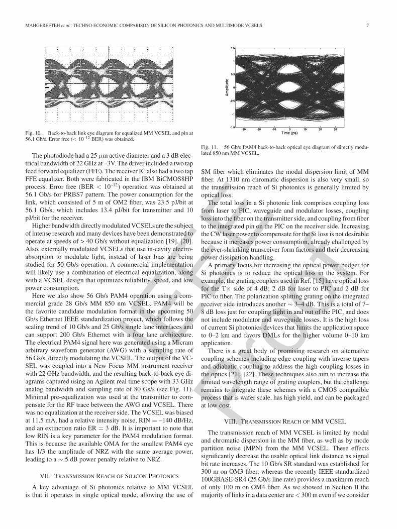
IEEE
Proo
f
MAHGEREFTEH et al.: TECHNO-ECONOMIC COMPARISON OF SILICON PHOTONICS AND MULTIMODE VCSELS 7
Fig. 10. Back-to-back link eye diagram for equalized MM VCSEL and pin at56.1 Gb/s. Error free (< 10–12 BER) was obtained.
The photodiode had a 25 μm active diameter and a 3 dB elec-trical bandwidth of 22 GHz at –3V. The driver included a two tapfeed forward equalizer (FFE). The receiver IC also had a two tapFFE equalizer. Both were fabricated in the IBM BiCMOS8HPprocess. Error free (BER < 10–12) operation was obtained at56.1 Gb/s for PRBS7 pattern. The power consumption for thelink, which consisted of 5 m of OM2 fiber, was 23.5 pJ/bit at56.1 Gb/s, which includes 13.4 pJ/bit for transmitter and 10pJ/bit for the receiver.
Higher bandwidth directly modulated VCSELs are the subjectof intense research and many devices have been demonstrated tooperate at speeds of > 40 Gb/s without equalization [19], [20].Also, externally modulated VCSELs that use in-cavity electro-absorption to modulate light, instead of laser bias are beingstudied for 50 Gb/s operation. A commercial implementationwill likely use a combination of electrical equalization, alongwith a VCSEL design that optimizes reliability, speed, and lowpower consumption.
Here we also show 56 Gb/s PAM4 operation using a com-mercial grade 28 Gb/s MM 850 nm VCSEL. PAM4 will bethe favorite candidate modulation format in the upcoming 50Gb/s Ethernet IEEE standardization project, which follows thescaling trend of 10 Gb/s and 25 Gb/s single lane interfaces andcan support 200 Gb/s Ethernet with a four lane architecture.The electrical PAM4 signal here was generated using a Micramarbitrary waveform generator (AWG) with a sampling rate of56 Gs/s, directly modulating the VCSEL. The output of the VC-SEL was coupled into a New Focus MM instrument receiverwith 22 GHz bandwidth, and the resulting back-to-back eye di-agrams captured using an Agilent real time scope with 33 GHzanalog bandwidth and sampling rate of 80 Gs/s (see Fig. 11).Minimal pre-equalization was used at the transmitter to com-pensate for the RF trace between the AWG and VCSEL. Therewas no equalization at the receiver side. The VCSEL was biasedat 11.5 mA, had a relative intensity noise, RIN = –140 dB/Hz,and an extinction ratio ER = 3 dB. It is important to note thatlow RIN is a key parameter for the PAM4 modulation format.This is because the available OMA for the smallest PAM4 eyehas 1/3 the amplitude of NRZ with the same average power,leading to a ∼ 5 dB power penalty relative to NRZ.
VII. TRANSMISSION REACH OF SILICON PHOTONICS
A key advantage of Si photonics relative to MM VCSELis that it operates in single optical mode, allowing the use of
Fig. 11. 56 Gb/s PAM4 back-to-back optical eye diagram of directly modu-lated 850 nm MM VCSEL.
SM fiber which eliminates the modal dispersion limit of MMfiber. At 1310 nm chromatic dispersion is also very small, sothe transmission reach of Si photonics is generally limited byoptical loss.
The total loss in a Si photonic link comprises coupling lossfrom laser to PIC, waveguide and modulator losses, couplingloss into the fiber on the transmitter side, and coupling from fiberto the integrated pin on the PIC on the receiver side. Increasingthe CW laser power to compensate for the Si loss is not desirablebecause it increases power consumption, already challenged bythe ever-shrinking transceiver form factors and their decreasingpower dissipation handling.
A primary focus for increasing the optical power budget forSi photonics is to reduce the optical loss in the system. Forexample, the grating couplers used in Ref. [15] have optical lossfor the T× side of 4 dB; 2 dB for laser to PIC and 2 dB forPIC to fiber. The polarization splitting grating on the integratedreceiver side introduces another ∼ 3–4 dB. This is a total of 7–8 dB loss just for coupling light in and out of the PIC, and doesnot include modulator and waveguide losses. It is the high lossof current Si photonics devices that limits the application spaceto 0–2 km and favors DMLs for the higher volume 0–10 kmapplication.
There is a great body of promising research on alternativecoupling schemes including edge coupling with inverse tapersand adiabatic coupling to address the high coupling losses inthe optics [21], [22]. These techniques also aim to increase thelimited wavelength range of grating couplers, but the challengeremains to integrate these schemes with a CMOS compatibleprocess that is wafer scale, has high yield, and can be packagedat low cost.
VIII. TRANSMISSION REACH OF MM VCSEL
The transmission reach of MM VCSEL is limited by modaland chromatic dispersion in the MM fiber, as well as by modepartition noise (MPN) from the MM VCSEL. These effectssignificantly decrease the usable optical link distance as signalbit rate increases. The 10 Gb/s SR standard was established for300 m on OM3 fiber, whereas the recently IEEE standardized100GBASE-SR4 (25 Gb/s line rate) provides a maximum reachof only 100 m on OM4 fiber. As we showed in Section II themajority of links in a data center are < 300 m even if we consider
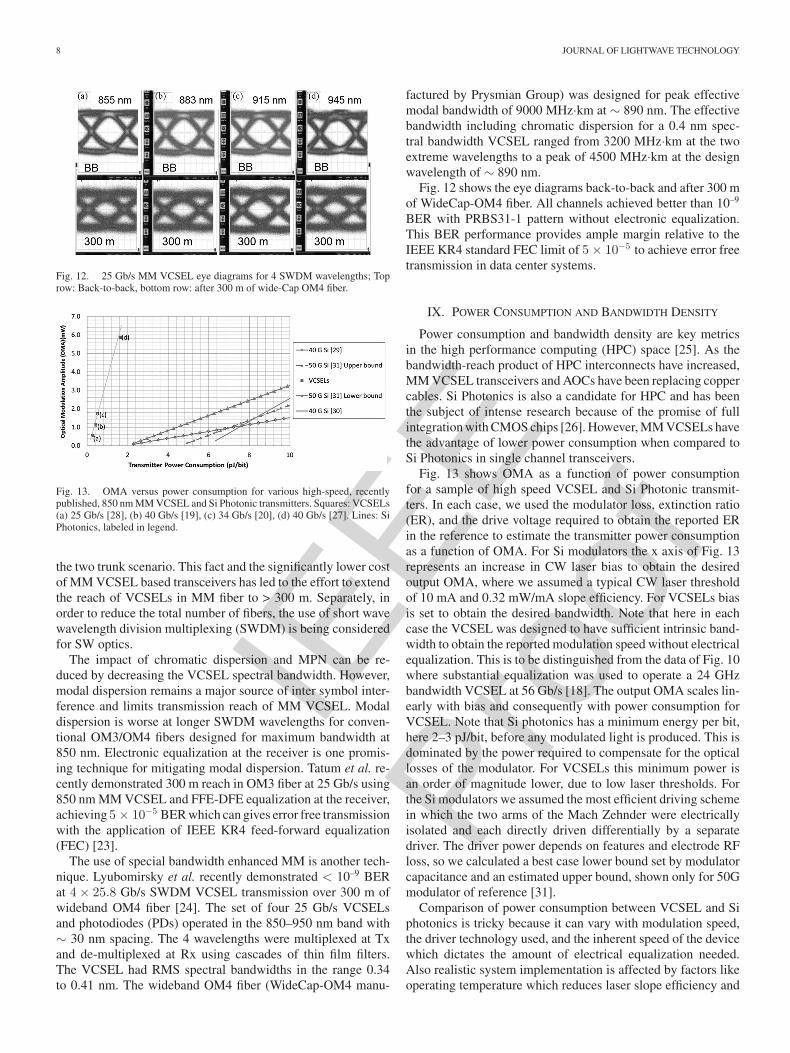
IEEE
Proo
f
8 JOURNAL OF LIGHTWAVE TECHNOLOGY
Fig. 12. 25 Gb/s MM VCSEL eye diagrams for 4 SWDM wavelengths; Toprow: Back-to-back, bottom row: after 300 m of wide-Cap OM4 fiber.
Fig. 13. OMA versus power consumption for various high-speed, recentlypublished, 850 nm MM VCSEL and Si Photonic transmitters. Squares: VCSELs(a) 25 Gb/s [28], (b) 40 Gb/s [19], (c) 34 Gb/s [20], (d) 40 Gb/s [27]. Lines: SiPhotonics, labeled in legend.
the two trunk scenario. This fact and the significantly lower costof MM VCSEL based transceivers has led to the effort to extendthe reach of VCSELs in MM fiber to > 300 m. Separately, inorder to reduce the total number of fibers, the use of short wavewavelength division multiplexing (SWDM) is being consideredfor SW optics.
The impact of chromatic dispersion and MPN can be re-duced by decreasing the VCSEL spectral bandwidth. However,modal dispersion remains a major source of inter symbol inter-ference and limits transmission reach of MM VCSEL. Modaldispersion is worse at longer SWDM wavelengths for conven-tional OM3/OM4 fibers designed for maximum bandwidth at850 nm. Electronic equalization at the receiver is one promis-ing technique for mitigating modal dispersion. Tatum et al. re-cently demonstrated 300 m reach in OM3 fiber at 25 Gb/s using850 nm MM VCSEL and FFE-DFE equalization at the receiver,achieving 5 × 10⁻⁵ BER which can gives error free transmissionwith the application of IEEE KR4 feed-forward equalization(FEC) [23].
The use of special bandwidth enhanced MM is another tech-nique. Lyubomirsky et al. recently demonstrated < 10–9 BERat 4 × 25.8 Gb/s SWDM VCSEL transmission over 300 m ofwideband OM4 fiber [24]. The set of four 25 Gb/s VCSELsand photodiodes (PDs) operated in the 850–950 nm band with∼ 30 nm spacing. The 4 wavelengths were multiplexed at Txand de-multiplexed at Rx using cascades of thin film filters.The VCSEL had RMS spectral bandwidths in the range 0.34to 0.41 nm. The wideband OM4 fiber (WideCap-OM4 manu-
factured by Prysmian Group) was designed for peak effectivemodal bandwidth of 9000 MHz·km at ∼ 890 nm. The effectivebandwidth including chromatic dispersion for a 0.4 nm spec-tral bandwidth VCSEL ranged from 3200 MHz·km at the twoextreme wavelengths to a peak of 4500 MHz·km at the designwavelength of ∼ 890 nm.
Fig. 12 shows the eye diagrams back-to-back and after 300 mof WideCap-OM4 fiber. All channels achieved better than 10–9
BER with PRBS31-1 pattern without electronic equalization.This BER performance provides ample margin relative to theIEEE KR4 standard FEC limit of 5 × 10⁻⁵ to achieve error freetransmission in data center systems.
IX. POWER CONSUMPTION AND BANDWIDTH DENSITY
Power consumption and bandwidth density are key metricsin the high performance computing (HPC) space [25]. As thebandwidth-reach product of HPC interconnects have increased,MM VCSEL transceivers and AOCs have been replacing coppercables. Si Photonics is also a candidate for HPC and has beenthe subject of intense research because of the promise of fullintegration with CMOS chips [26]. However, MM VCSELs havethe advantage of lower power consumption when compared toSi Photonics in single channel transceivers.
Fig. 13 shows OMA as a function of power consumptionfor a sample of high speed VCSEL and Si Photonic transmit-ters. In each case, we used the modulator loss, extinction ratio(ER), and the drive voltage required to obtain the reported ERin the reference to estimate the transmitter power consumptionas a function of OMA. For Si modulators the x axis of Fig. 13represents an increase in CW laser bias to obtain the desiredoutput OMA, where we assumed a typical CW laser thresholdof 10 mA and 0.32 mW/mA slope efficiency. For VCSELs biasis set to obtain the desired bandwidth. Note that here in eachcase the VCSEL was designed to have sufficient intrinsic band-width to obtain the reported modulation speed without electricalequalization. This is to be distinguished from the data of Fig. 10where substantial equalization was used to operate a 24 GHzbandwidth VCSEL at 56 Gb/s [18]. The output OMA scales lin-early with bias and consequently with power consumption forVCSEL. Note that Si photonics has a minimum energy per bit,here 2–3 pJ/bit, before any modulated light is produced. This isdominated by the power required to compensate for the opticallosses of the modulator. For VCSELs this minimum power isan order of magnitude lower, due to low laser thresholds. Forthe Si modulators we assumed the most efficient driving schemein which the two arms of the Mach Zehnder were electricallyisolated and each directly driven differentially by a separatedriver. The driver power depends on features and electrode RFloss, so we calculated a best case lower bound set by modulatorcapacitance and an estimated upper bound, shown only for 50Gmodulator of reference [31].
Comparison of power consumption between VCSEL and Siphotonics is tricky because it can vary with modulation speed,the driver technology used, and the inherent speed of the devicewhich dictates the amount of electrical equalization needed.Also realistic system implementation is affected by factors likeoperating temperature which reduces laser slope efficiency and

IEEE
Proo
f
MAHGEREFTEH et al.: TECHNO-ECONOMIC COMPARISON OF SILICON PHOTONICS AND MULTIMODE VCSELS 9
increases bias, for example. 100 Gb/s (4 × 25 Gb/s/lane) isa good application to compare the two technologies as it isthe highest rate that is commercially available for VCSEL andSi photonics and becoming widely deployed. Webster et al.[32] and Cignoli et al. [33] recently reported commercially vi-able silicon photonic modulators where the modulation functionrequires 6–11 pJ/bit. This is also consistent with PSM4 appli-cations using silicon photonics having to meet 3.5 W worst-case power consumption allowed for the QSFP28 form factor.Adding the power consumption of the CW laser this translatesto total of 8–13 pJ/bit at 25 Gb/s for Si photonic transmit-ter. In the first generation VCSEL-based products operating at100 Gb/s (4 × 25 Gb/s) the transmitter function consumes 5pJ/bit including laser bias. Next generation VCSEL products,which use lower power driver technology are targeted to con-sume 2–3 pJ/bit for the transmitter including laser bias. As onesuch example, Shibata et al. has demonstrated a commerciallyavailable 850-nm VCSEL with 1.8 pJ/bit power consumption at25.7 Gb/s using a 65-nm CMOS driver [34].
The bandwidth density, which is important for board mount-able optics and chip-to-chip interconnects, is a function of elec-trical and optical interfaces, but VCSELs have a smaller footprint than Si Photonics, so they have the potential for achiev-ing higher bandwidth density. A typical VCSEL aperture is∼ 8 μm. A Si photonics modulator foot print, on the other hand,is ∼300 μm and the CW laser is 300 μm–1 mm. Also spacehas to be reserved for coupling optics; e.g., grating coupler androuting to the modulator in the Si PIC. To the best of our knowl-edge, the highest bandwidth density demonstrated so far for anoptical interconnect is 64 Gb/s/mm2 using VCSEL mounted ona switch ASIC [35]. However bandwidth density should not beevaluated in isolation from other attributes because increasingit necessitates closer integration of optics and ASIC, which canbe a drawback for yield, reliability and serviceability [25].
X. CONCLUSION
We believe MM VCSELs will continue to dominate the datacenter and HPC interconnect markets, driven by favorable eco-nomics that are unlikely to change soon. Si Photonics is a goodfit for new mega data centers where SM fiber is used in structuredcabling as long as packaging issues are successfully solved to en-able competitive cost and allow use in both pluggable transceiverand board mountable optical engines.
REFERENCES
[1] (2015). [Online]. Available: http://www.molex.com.[2] A. Narasimha, B. Analui, E. Balmater, A. Clark, T. Gal, D. Gucken-
berger, S. Gutierrez, M. Harrison, R. Ingram, R. Koumans, D. Kucharski,K. Leap, Yi. Liang, A. Mekis, S. Mirsaidi, M. Peterson, T. Pham,T. Pinguet, D. Rines, V. Sadagopan, T. J. Sleboda, D. Song, Y. Wang,B. Welch, J. Witzens, S. Abdalla, S. Gloeckner, and P. De Dobbelaere, “A40-Gb/s QSFP optoelectronic transceiver in a 0.13 μm CMOS silicon-on-insulator technology,” presented at the Opt. Fiber Communications Conf.,Carlsbad, CA, USA, 2008, Paper MK7.
[3] C. Sciancalepore, R. J. Lycett, J. A. Dallery, S. Pauliac, K. Hassan,J. Harduin, H. Duprez, U. Weidenmueller, D. F. G. Gallagher, S. Menezo,and B. Ben Bakir, “Low-crosstalk fabrication-insensitive Echelle gratingdemultiplexers on silicon-on-insulator,” IEEE Photon. Technol. Lett., vol.27, no. 5, pp. 494–497, Mar. 2015.
[4] G. Denoyer, A. Chen, B. Park, Z. Yuxin, A. Santipo, and R. Russo,“Hybrid silicon photonic circuits and transceiver for 56 Gb/s NRZ 2.2 km
transmission over single mode fiber,” presented at the European Conf.Optical Communication, Cannes, France, 2014.
[5] (2015, May). [Online]. Available: http://www.ieee802.org/3/bs/public/15_05/welch_3bs_01a_0515.pdf
[6] A. Narasimha et al., “An ultralow power CMOS photonics technologyplatform for H/S optoelectronics transceivers at less than $1 per Gbps,”presented at the Optical Fiber Communications Conf., San Diego, CA,USA, 2010, Paper OMV4.
[7] (2015). [Online]. Available: http://www.macom.com/products/photonic-solutions/distributed-feedback-lasers.
[8] A. Descos, C. Jany, D. Bordel, H. Duprez, G. Beninca-de-Farias, P.Brianceau,, S. Menezo, and B. Ben Bakir, “Heterogeneously integratedIII–V/Si distributed Bragg reflector laser with adiabatic coupling,” pre-sented at the European Conf. Optical Communication, London, U.K.,2013.
[9] (2015). [Online]. Available: www.psm4.org[10] S. Joblot et al., “Copper pillar interconnect capability for mmwave ap-
plications in 3D integration technology,” Microelectron. Eng., vol. 107pp. 72–79, 2013.
[11] M. Streshinsky et al., “Low power 50 Gb/s silicon traveling wave Mach-Zehnder modulator near 1300 nm,” Opt. Exp., vol. 21, no. 25, pp. 30350–30357, Dec 2013.
[12] Xi. Xiao et al., “High-speed, low-loss silicon Mach–Zehnder modulatorswith doping optimization,” Opt. Exp., vol. 21, no. 4, pp. 4116–4125, Feb2013.
[13] A. Shastri et al., “Ultra-low-power single-polarization QAM-16 gener-ation without DAC using a CMOS photonics based segmented modu-lator,” IEEE J. Lightw. Technol., vol. 33, no. 6, pp. 1255–1260, Mar.2015.
[14] Ran. Ding et al., “100-Gb/s NRZ optical transceiver analog front-end in130-nm SiGe BiCMOS,” presented at the Optical Interconnects Conf.,San Diego, CA, USA, 2014.
[15] G. Denoyer et al., “Hybrid silicon photonic circuits and transceiver for 50gb/s NRZ transmission over single-mode fiber,” IEEE J. Lightw. Technol.,vol. 33, no. 6, pp. 1247–1254, Mar 2015.
[16] F. Boeuf et al., “A multi-wavelength 3D-compatible silicon photonicsplatform on 300 mm SOI wafers for 25 Gb/s applications,” in Proc. IEEEInt. Electron. Devices Meet., 2013, pp. 13.3.1–13.3.4.
[17] Y. Matsui et al. “112 Gb/s WDM link using two directly modu-lated Al-MQW BH DFB lasers at 56 Gb/s,” presented at the Op-tical Fiber Communications Conf., Los Angeles, CA, USA, 2015,Paper Th5B6.
[18] D. M. Kuchta et al., “A 56.1Gb/s NRZ modulated 850nm VCSEL-basedoptical link,” presented at the Optical Fiber Communications Conf., Ana-heim, CA, USA, 2013, Paper OW1B5.
[19] Westberg et al., “High-speed oxide confined 850 nm VCSELs operatingerror free at 40 Gb/s up to 85 C,” IEEE Photon. Technol. Lett., vol. 25,no. 8, pp. 768–771, Apr. 2013.
[20] J.-W. Shi et al., “Oxide-relief and Zn-diffusion 850 nm vertical cavitysurface emitting lasers with extremely low energy to data rate ratios for40 Gb/s operations,” IEEE J. Sel. Topics Quantum Electron., vol. 19,no. 2, p. 7900208, Mar./Apr. 2013.
[21] T. Barwicz, A. Janta-Polczynski, M. Khater, Y. Thibodeau, R. Leidy,J. Maling, S. Martel, S. Engelmann, J. S. Orcutt, P. Fortier, and W.M. J. Green, “An o-band metamaterial converter interfacing standardoptical fibers to silicon nanophotonic waveguides,” presented at theOptical Fiber Communication Conf., Los Angeles, CA, USA, 2015,Paper Th3F3.
[22] R. Dangel, J. Hofrichter, F. Horst, D. Jubin, A. La Porta, N. Meier, I. M.Soganci, J. Weiss, and B. J. Offrein, “Polymer waveguides for electro-optical integration in data centers and high-performance computers,” Opt.Exp., vol. 23, no. 4, pp. 4736–4750, 2015.
[23] J. A. Tatum, D. Gazula, L. A. Graham, J. K. Guenter, R. H. Johnson,J. King, C. Kocot, G. D. Landry, I. Lyubomirsky, A. N. MacInnes,E. M. Shaw, K. Balemarthy, R. Shubochkin, D. Vaidya, M. Yan, and F.Tang, “VCSEL-based interconnects for current and future data centers,”J. Lightw. Technol., vol. 33, no. 4, pp. 727–732, Feb. 15, 2015.
[24] I. Lyubomirsky, R. Motaghian, H. Daghighian, D. McMahon, S. Nelson,C. Kocot, J. A. Tatum, F. Achten, P. Sillard, D. Molin, and A. Amezcua-Correa, “100G SWDM4 transmission over 300 m wideband MMF,” inProc. Eur. Conf. Opt. Commun., 2015, paper P. 5. 4.
[25] M. A. Taubenblatt, “Optical interconnects for high performance comput-ing,” J. Lightw. Technol., vol. 30, no. 4, pp. 448–457, Feb. 2012.
[26] X. Zheng and A. V. Krishnamoorthy, “Si photonics technology for futureoptical interconnection,” presented at the Communications and Photon.Conf. Exhib., Shanghai, China, 2011.

IEEE
Proo
f
10 JOURNAL OF LIGHTWAVE TECHNOLOGY
[27] P. Wolf, P. Moser, G. Larisch, H. Li, J. A. Lott, and D. Bimberg, “En-ergy efficient 40 Gb/s transmission with 850 nm VCSELs at 108 fJ/bitdissipated heat,” Electron. Lett., vol. 49, no. 10, pp. 666–667, 2013.
[28] P. Moser, J. A. Lott, D. Bimberg, “Energy efficiency of directly modulatedoxide-confined high bit rate 850 nm VCSELs for optical interconnect,”IEEE J. Sel. Topics Quantum Electron., vol. 19, no. 4 p. 1702212, Jul./Aug.2013.
[29] D. J. Thomson et al., “High contrast 40 Gbit/s optical modulation insilicon,” Opt. Exp., vol. 19, no. 12, pp. 11507–11516, 2011.
[30] P. Dong et al., “High-speed low-voltage single-drive push-pull siliconMach-Zehnder modulators,” Opt. Exp., vol. 20, pp. 6163–6169, 2012.
[31] X. Xiao et al., “High-speed, low-loss silicon Mach–Zehnder modulatorswith doping optimization,” Opt. Exp., vol. 21, pp. 4116–4125, 2013.
[32] M. Webster et al., “Silicon photonic modulator based on a MOS-capacitorand a CMOS driver,” presented at the Compound Semicond. IntegratedCircuit Symp., La Jolla, CA, USA, 2015, paper Session E.
[33] M. Cignoli et al., “A 1310-nm 3-D integrated silicon photonics Mach–Zehnder-based modulator transmitter with 275 mW multi-stage CMOSdriver achieving 6dB extinction ratio at 25Gb/s,” in Proc. IEEE Int. SolidState Circ. Conf., 2015, Session 22.9.
[34] M. Shibata et al., “26Gb/s 1.8-pJ/bit CMOS-driven transmitter for 850-nm common cathode VCSELs,” presented at the Optical Fiber Conf., LosAngles, CA, USA, 2015, Paper OTu3G.1.
[35] K. Hasharoni et al., “A high end routing platform for core and edgeapplications based on chip to chip optical interconnect,” presented at theOpt. Fiber Conf., Anaheim, CA, USA, 2013, Paper OTu3H.2.
Daniel Mahgerefteh was born in Isfahan, Iran, in 1963. He received the Ph.D.degree in physics from the University of Southern California, Los Angeles, CA,USA, in 1990. He was a Research Faculty with the Laboratory for Physical Sci-ences, University of Maryland from 1993 to 2000. He is currently the director ofthe advanced technology at Finisar Corporation, Sunnyvale, CA, USA, workingon integrated photonics and low cost packaging technologies for data commu-nications market. He was the Cofounder and Chief Technology Officer of AznaLLC and the coinventor of the Chirp Managed Laser technology. He has morethan 50 issued or pending patents and is the author of numerous publications.
Craig Thompson received the Bachelor of Engineering (Hons.) degree from theUniversity of New South Wales, Sydney, N.S.W, Australia, and the MBA degreefrom the Massachusetts Institute of Technology, Cambridge, MA, USA. He iscurrently the Director of Strategic Marketing at Finisar Corporation, Sunnyvale,CA, USA. His research interests include long-term product and technologyroadmaps for optical communications, and contributes to advanced developmentactivities supporting the roadmaps. He has held a number of marketing andproduct management roles in optical communications, networking, and storagein companies such as Intel, Gennum, and EMC, spanning 15 years.
Chris Cole received the B.S. degree in aeronautics and astronautics, and the B.S.and M.S. degrees in electrical engineering, all from the Massachusetts Instituteof Technology, Cambridge, MA, USA. He is currently the Director at FinisarCorporation, Sunnyvale, CA, USA, where he is architecting and leading the de-velopment of 50-, 100-, 200-, and 400-Gb/s optical interfaces and transceivers.At Hughes Aircraft Co. (currently Boeing SDC) and then the M.I.T. LincolnLaboratory, he contributed to multiple imaging and communication satelliteprograms such as Milstar. He later consulted on telecom ASIC architecturesand designs for Texas Instruments DSP Group and Silicon Systems, Inc. (cur-rently Maxim.). He was one of the architects of the Sequoia coherent imagingultrasound platform at Acuson Corp. (currently Siemens Ultrasound), where healso managed hardware and software groups. As a Principal Consultant with theParallax Group he carried out signal processing analysis and product definitionfor several imaging and communication systems. At BBN, a Finisar acquisition,he developed 10 Gb/s and 40 Gb/s optical transceivers.
Gilles Denoyer (M’02) received the M.S. degree from Supelec EngineeringSchool, Gif Sur Yvette, France, in 1995. In 1996, he was with SGS-ThomsonMicroelectronics (STMicroelectronics since 1998), San Jose, CA, USA, and wasinvolved with the design of MR preamplifiers for hard disk drives. In 2002, hewas with Finisar Corporation, Sunnyvale, CA, where he worked on the design oftransimpedance amplifiers, CDRs, and 100G Gearbox ICs. His current researchinterests include silicon photonics and high-speed circuits for next generationfiber optics transceivers.
Thelinh Nguyen received the Bachelor’s of Engineering and Master.s of Engi-neering degrees from the University of Waterloo, Waterloo, ON, Canada, andQueen’s University, Kingston, ON, Canada, respectively. He is currently theDirector of IC Engineering at Finisar Corporation, Sunnyvale, CA, USA. Heworks on optical front-ends and retiming circuits for 100G and 400G opticaltransceiver products. Since 1999, he has been with Finisar Corporation. Prior toFinisar, he spent seven years with Nortel Networks developing IC’s and modulesfor OC-192 and OC-768 applications.
Ilya Lyubomirsky received the Ph.D. degree in electrical engineering fromMassachusetts Institute of Technology, Cambridge, MA, USA, in 1999. Early inhis career at Telcordia and ONI Systems Inc., he contributed to system modelingand design of high-speed packet and optical metro networks. He developedultradense WDM transmission systems at Ciena Corporation, and involved inthe research of PIC-based fiber-optic communications at Infinera Corporation.From 2003 to 2010, he was an electrical engineering Faculty at University ofCalifornia, Riverside. He is currently at the Finisar Corporation, Sunnyvale, CA,USA, involved in research work of advanced modulation, DSP algorithms, andcoding techniques to enable advanced optical modules for 100/400 Gb/s, etc.He has coauthored about 50 peer-reviewed journals, conference papers, and tenpatents.
Chris Kocot received the Ph.D. degree in electrical engineering under an ex-change program between Warsaw University, Warszawa, Poland, and StanfordUniversity, Stanford, CA, USA. He is the Director at Finisar Corporation, Sun-nyvale, CA, where he provides technical leadership to R & D projects in the areaof high-speed module design, microwave and signal-integrity simulations, andoptics design. He is also working on high-speed VCSEL development projects.He was with the Hewltt-Packard Laboratories, Palo Alto, CA, as a Member ofTechnical Staff on MESFETs and later on HEMTs and subsequently on high-speed photo-detectors, APDs, LEDs, and VCSELs. He became a Departmentmanager at the Agilent Fiber-Optics Division, San Jose, CA. His departmentdeveloped state of the art 850 and 980 nm VCSELs and high-speed photo-detectors (APDs and photo-HBT). He then joined Novalux, Inc., Sunnyvale,CA, as the Director of the Laser Engineering Group. He led the developmentof high-power red, green, and blue external-cavity lasers from their infancy tomaturity with proven reliability and high power in the visible range (3W red, 8Wgreen, and 8W blue). He has more than 20 patents related to photo-detectors,APDs, HEMTs, ICs, LEDs, and VCSELs.
Jim Tatum was born in Hayward, CA, USA, in 1967. He received the B.A.degree from Austin College, Sherman, TX, USA, in 1989, and the M.S. andPh.D. degrees from the University of Texas, Dallas, TX, in 1992 and 1995,respectively. He was with Honeywell in 1996 as a VCSEL Design Engineerafter a brief stint with the Polaroid Corporation. He is currently the Directorof VCSEL and Photodiode product development in Finisar Corporation, Allen,TX. He has been the author of more than 30 technical papers and holds morethan 30 patents.