Embed Size (px)
Citation preview
Pr. Mustapha AIT ALI
Soft chemical synthesis
of nanostructured
materials
Laboratoire de Chimie de Coordination et Catalyse
Université Cadi Ayyad - Faculté des Sciences-semlalia
Marrakech –Morroco
E-mail: [email protected]
1
ACRICE 2017 Setif, Algeria, 8-11 October 2017
Université Ferhat ABBAS Sétif-1, Algérie
2 Outline
✓ Introduction
o Nanometer and history of nanomaterial
o Applications and economic issues
✓ Chemical Approaches to nanomaterials
✓ Metallic nanoparticles and Nanostructured
metallic oxides
✓ 2D Materials:
o Silicon nanosheets (SiNSs) and silicene
o Black phosphorus and phosphorene
✓ Conclusion
ACRICE 2017 Setif, Algeria, 8-11 October 2017
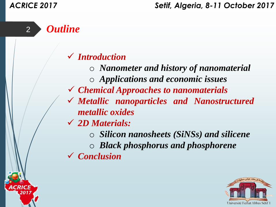
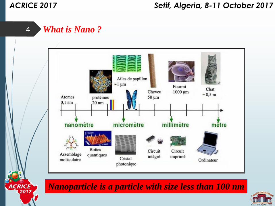
3 What is Nano ?
✓ thousand times smaller than a micron.
✓ about 500,000 times finer than the thickness of
the ballpoint pen,
✓ 30,000 times finer than the thickness of a hair
✓ 100 times smaller than the DNA molecule.
The prefix « nano » :
Greek origin, means «very small».
One nanometer (nm) one billionth of a meter (10-9 meter).
ACRICE 2017 Setif, Algeria, 8-11 October 2017
4
Nanoparticle is a particle with size less than 100 nm
ACRICE 2017 Setif, Algeria, 8-11 October 2017
What is Nano ?
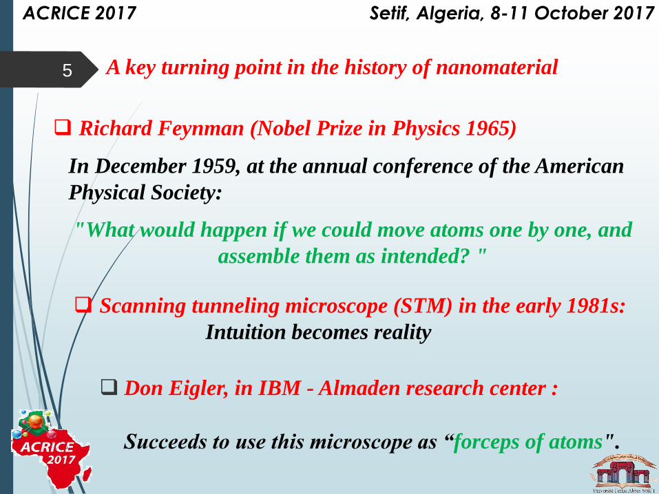
Don Eigler, in IBM - Almaden research center :
Succeeds to use this microscope as “forceps of atoms".
5
Richard Feynman (Nobel Prize in Physics 1965)
In December 1959, at the annual conference of the American
Physical Society:
"What would happen if we could move atoms one by one, and
assemble them as intended? "
Scanning tunneling microscope (STM) in the early 1981s:
Intuition becomes reality
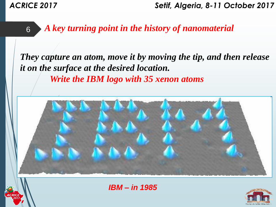
A key turning point in the history of nanomaterial
ACRICE 2017 Setif, Algeria, 8-11 October 2017
6
They capture an atom, move it by moving the tip, and then release
it on the surface at the desired location.
Write the IBM logo with 35 xenon atoms
IBM – in 1985
A key turning point in the history of nanomaterial
ACRICE 2017 Setif, Algeria, 8-11 October 2017
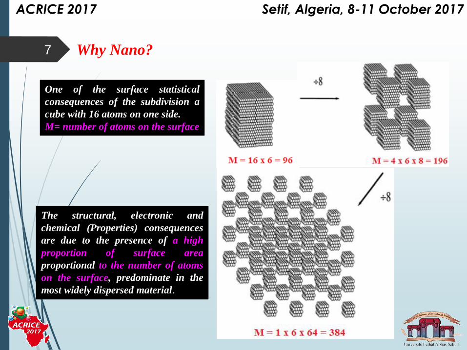
The structural, electronic and
chemical (Properties) consequences
are due to the presence of a high
proportion of surface area
proportional to the number of atoms
on the surface, predominate in the
most widely dispersed material.
7
One of the surface statistical
consequences of the subdivision a
cube with 16 atoms on one side.
M= number of atoms on the surface
Why Nano?
ACRICE 2017 Setif, Algeria, 8-11 October 2017
8
Since nanomaterials possess unique,
beneficial chemical, physical, and
mechanical properties, they can be
used for a wide variety of applications.
These applications include, but are
not limited to, the following:
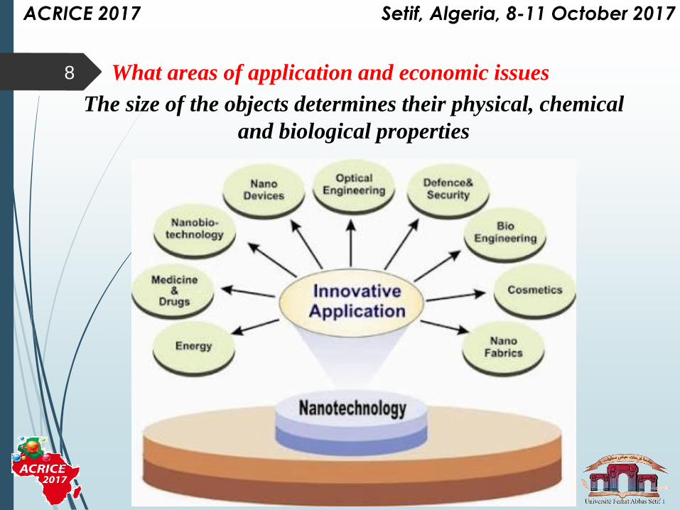
The size of the objects determines their physical, chemical
and biological properties
What areas of application and economic issues
ACRICE 2017 Setif, Algeria, 8-11 October 2017
9
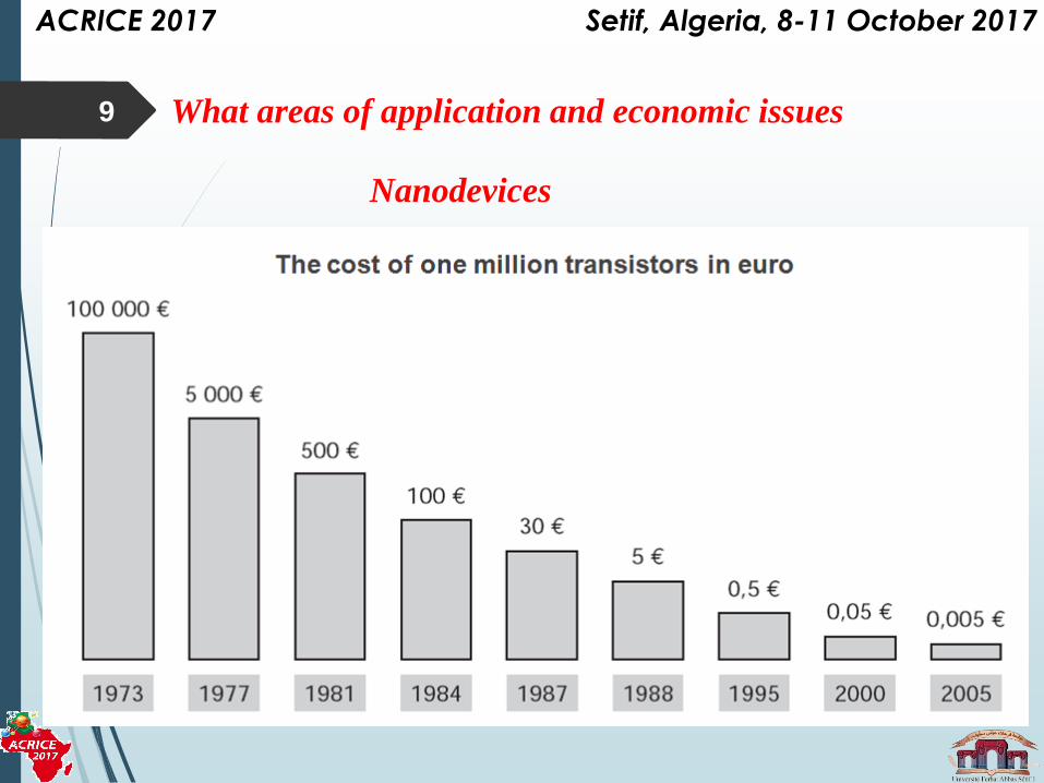
Nanodevices
Size and number of transistors in an integrated circuit
What areas of application and economic issues
ACRICE 2017 Setif, Algeria, 8-11 October 2017
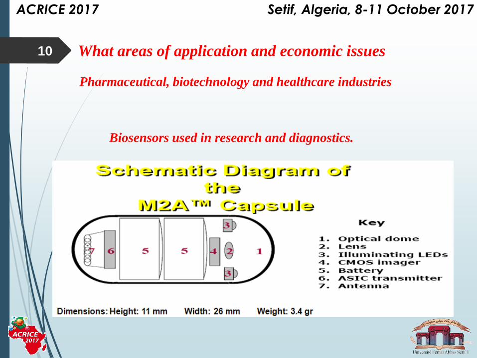
Biosensors used in research and diagnostics.
10
Pharmaceutical, biotechnology and healthcare industries
What areas of application and economic issues
ACRICE 2017 Setif, Algeria, 8-11 October 2017
11
12 Outline
✓ Introduction
o NanomApplications and economic issues
o eter and history of nanomaterial
✓ Chemical Approaches to nanomaterials
ACRICE 2017 Setif, Algeria, 8-11 October 2017
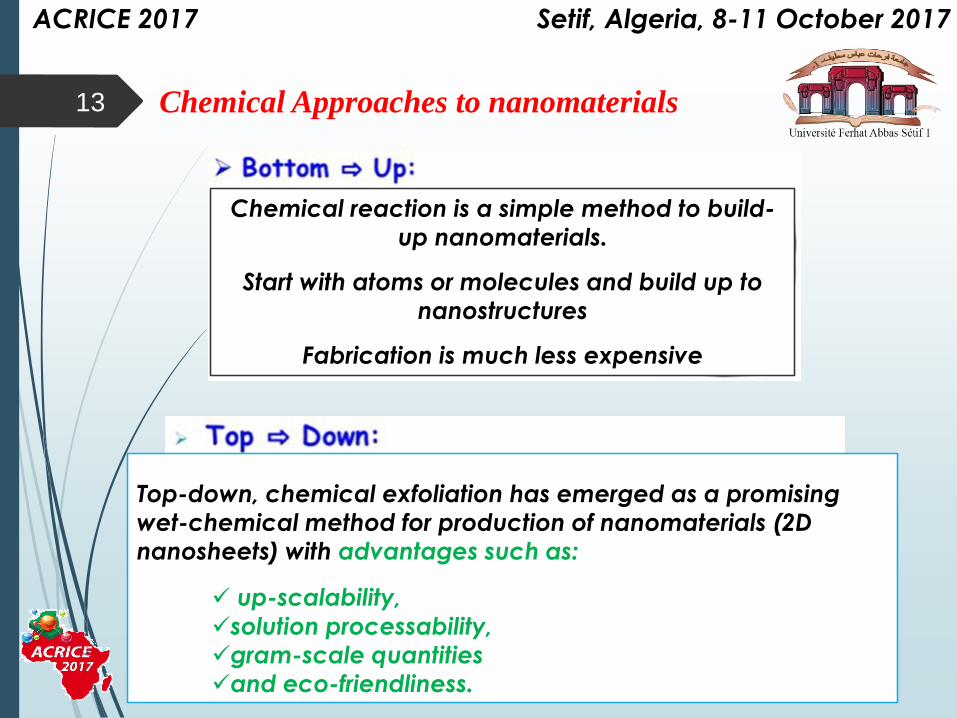
13 Chemical Approaches to nanomaterials
ACRICE 2017 Setif, Algeria, 8-11 October 2017
Chemical reaction is a simple method to build-
up nanomaterials.
Start with atoms or molecules and build up to
nanostructures
Fabrication is much less expensive
Top-down, chemical exfoliation has emerged as a promising
wet-chemical method for production of nanomaterials (2D
nanosheets) with advantages such as:
✓ up-scalability,
✓solution processability,
✓gram-scale quantities
✓and eco-friendliness.
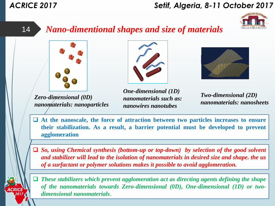
Zero-dimensional (0D)
nanomaterials: nanoparticles
One-dimensional (1D)
nanomaterials such as:
nanowires nanotubes
Nano-dimentional shapes and size of materials14
Two-dimensional (2D)
nanomaterials: nanosheets
ACRICE 2017 Setif, Algeria, 8-11 October 2017
At the nanoscale, the force of attraction between two particles increases to ensure
their stabilization. As a result, a barrier potential must be developed to prevent
agglomeration
So, using Chemical synthesis (bottom-up or top-down) by selection of the good solvent
and stabilizer will lead to the isolation of nanomaterials in desired size and shape. the us
of a surfactant or polymer solutions makes it possible to avoid agglomeration.
These stabilizers which prevent agglomeration act as directing agents defining the shape
of the nanomaterials towards Zero-dimensional (0D), One-dimensional (1D) or two-
dimensional nanomaterials.
15
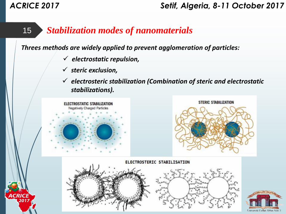
Threes methods are widely applied to prevent agglomeration of particles:
Stabilization modes of nanomaterials
✓ electrosteric stabilization (Combination of steric and electrostatic stabilizations).
✓ electrostatic repulsion,
✓ steric exclusion,
ACRICE 2017 Setif, Algeria, 8-11 October 2017
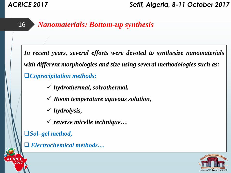
16 Nanomaterials: Bottom-up synthesis
ACRICE 2017 Setif, Algeria, 8-11 October 2017
In recent years, several efforts were devoted to synthesize nanomaterials
with different morphologies and size using several methodologies such as:
Coprecipitation methods:
✓ hydrothermal, solvothermal,
✓ Room temperature aqueous solution,
✓ hydrolysis,
✓ reverse micelle technique…
Sol–gel method,
Electrochemical methods…
Size control by water-soluble protective agents
NaBH4
growthphase
Suitable for H2O
Chemicalreduction
17
ACRICE 2017 Setif, Algeria, 8-11 October 2017
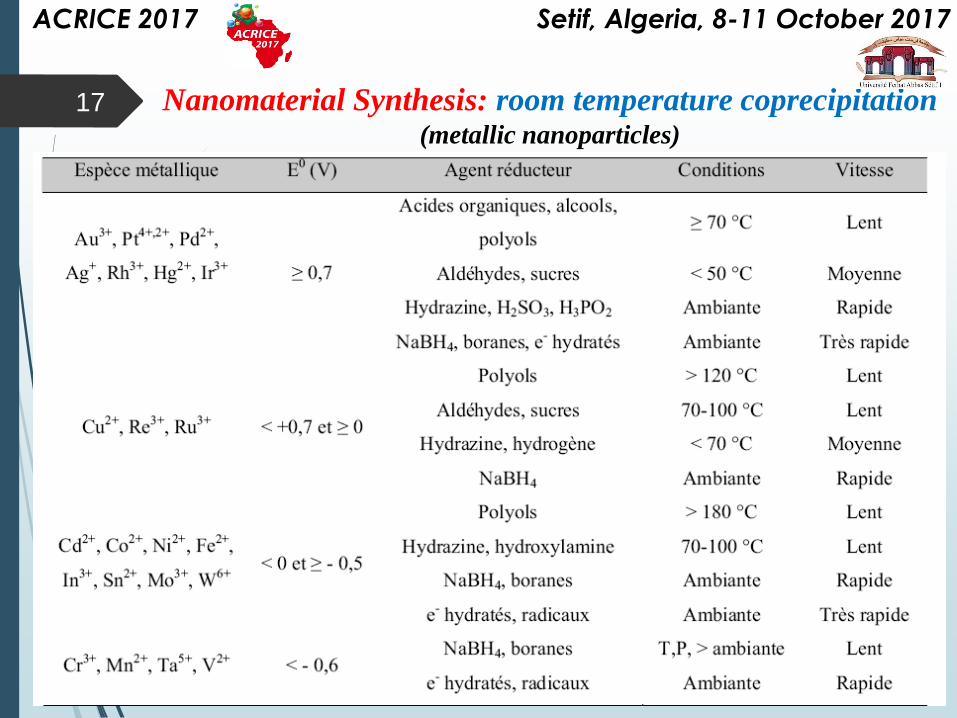
Nanomaterial Synthesis: room temperature coprecipitation(metallic nanoparticles)
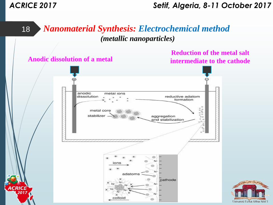
Anodic dissolution of a metalReduction of the metal salt
intermediate to the cathode
18
ACRICE 2017 Setif, Algeria, 8-11 October 2017
Nanomaterial Synthesis: Electrochemical method(metallic nanoparticles)
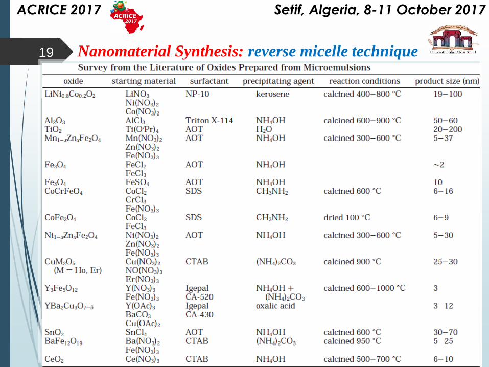
19 Nanomaterial Synthesis: reverse micelle technique
ACRICE 2017 Setif, Algeria, 8-11 October 2017
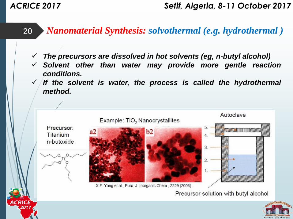
20
✓ The precursors are dissolved in hot solvents (eg, n-butyl alcohol)
✓ Solvent other than water may provide more gentle reaction
conditions.
✓ If the solvent is water, the process is called the hydrothermal
method.
Nanomaterial Synthesis: solvothermal (e.g. hydrothermal )
ACRICE 2017 Setif, Algeria, 8-11 October 2017
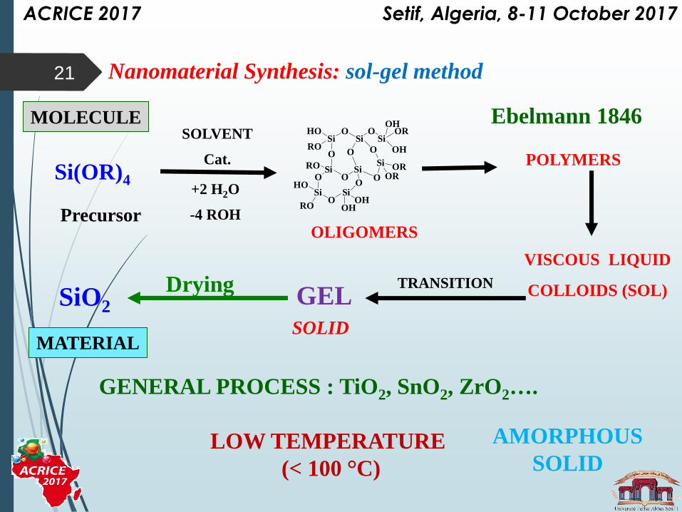
21
Ebelmann 1846
GENERAL PROCESS : TiO2, SnO2, ZrO2….
LOW TEMPERATURE
(< 100 °C)
+2 H2O
-4 ROH
SOLVENT
Cat.
AMORPHOUS
SOLID
OLIGOMERS
HOSi
OSi
OSi
OR
O O OHRO
SiO
Si
O
OH
O
O
SiO
RO
RO
HOSi
OH
Si
O
OH
OROR
POLYMERS
GELSOLID
TRANSITIONDrying
MATERIAL
SiO2
Si(OR)4
Precursor
MOLECULE
VISCOUS LIQUID
COLLOIDS (SOL)
Nanomaterial Synthesis: sol-gel method
ACRICE 2017 Setif, Algeria, 8-11 October 2017
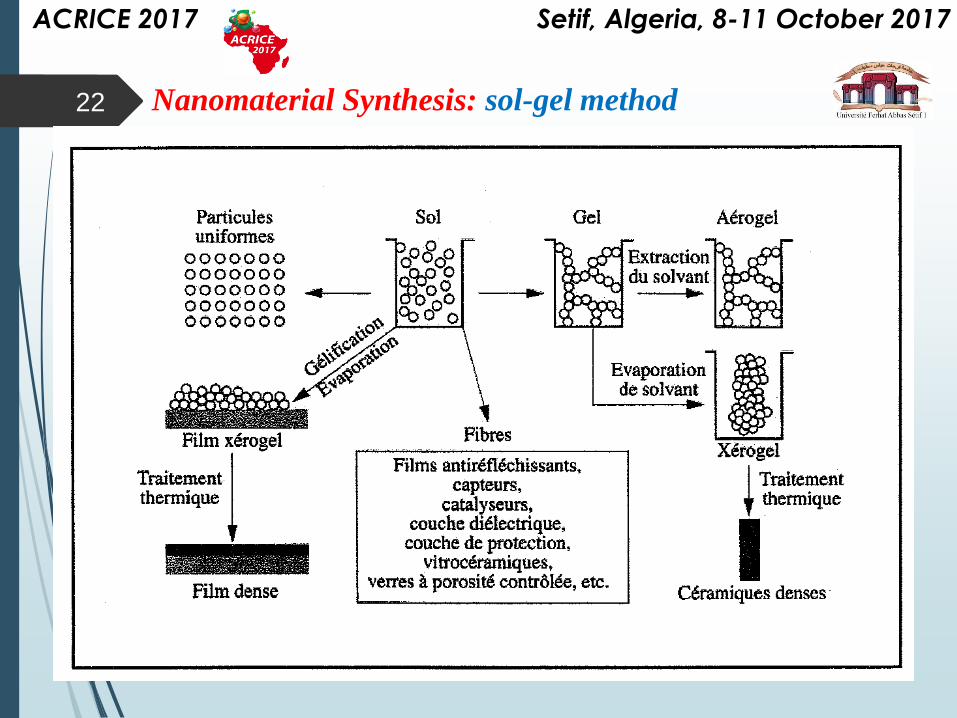
22 Nanomaterial Synthesis: sol-gel method
ACRICE 2017 Setif, Algeria, 8-11 October 2017
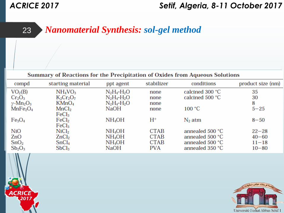
23 Nanomaterial Synthesis: sol-gel method
ACRICE 2017 Setif, Algeria, 8-11 October 2017
24 Outline
✓ Introduction
o Nanometer and history of nanomaterial
o Applications and economic issues
✓ Chemical Approaches to nanomaterials
✓ Metallic nanoparticles and Nanostructured
metallic oxides (some results)
✓ 2D Materials:
o Silicon nanosheets (SiNSs) and silicene
o Black phosphorus and phosphorene
✓ Conclusion
ACRICE 2017 Setif, Algeria, 8-11 October 2017
25
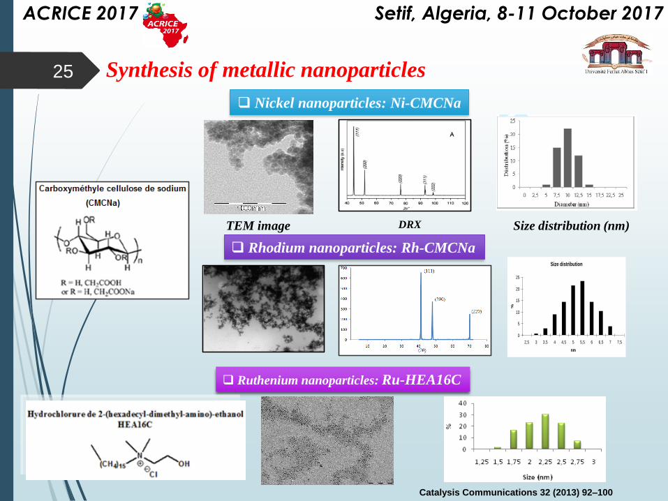
TEM image DRX Size distribution (nm)
Catalysis Communications 32 (2013) 92–100
Nickel nanoparticles: Ni-CMCNa
Synthesis of metallic nanoparticles
Rhodium nanoparticles: Rh-CMCNaSize distribution
0
5
10
15
20
25
2,5 3 3,5 4 4,5 5 5,5 6 6,5 7 7,5
nm
%
Ruthenium nanoparticles: Ru-HEA16C
ACRICE 2017 Setif, Algeria, 8-11 October 2017
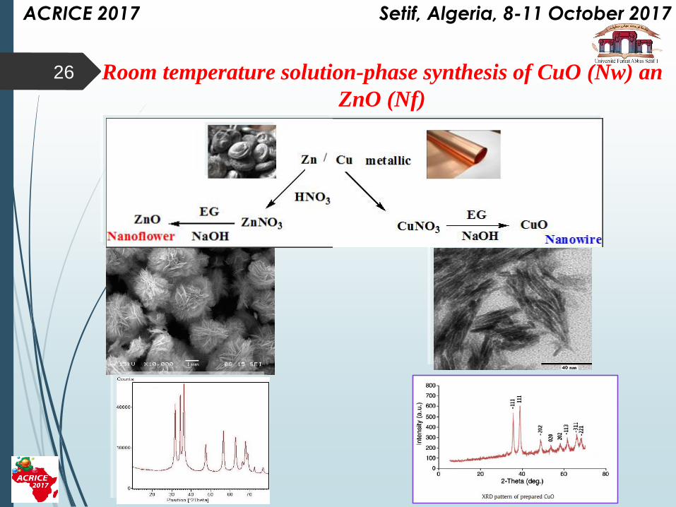
26 Room temperature solution-phase synthesis of CuO (Nw) an
ZnO (Nf)
ACRICE 2017 Setif, Algeria, 8-11 October 2017
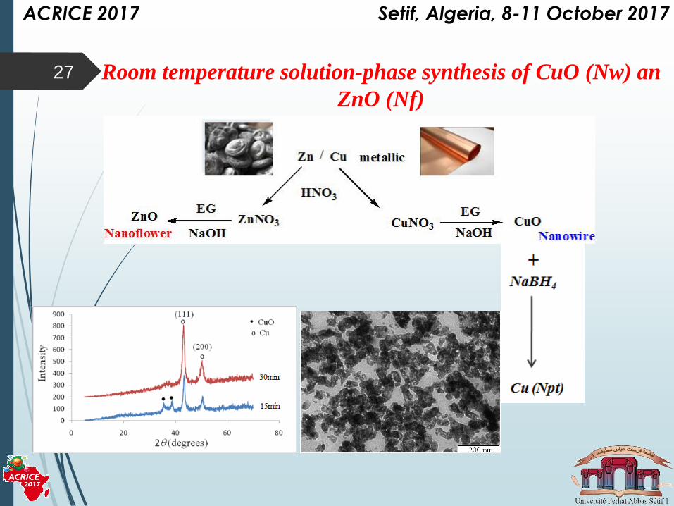
27 Room temperature solution-phase synthesis of CuO (Nw) an
ZnO (Nf)
ACRICE 2017 Setif, Algeria, 8-11 October 2017
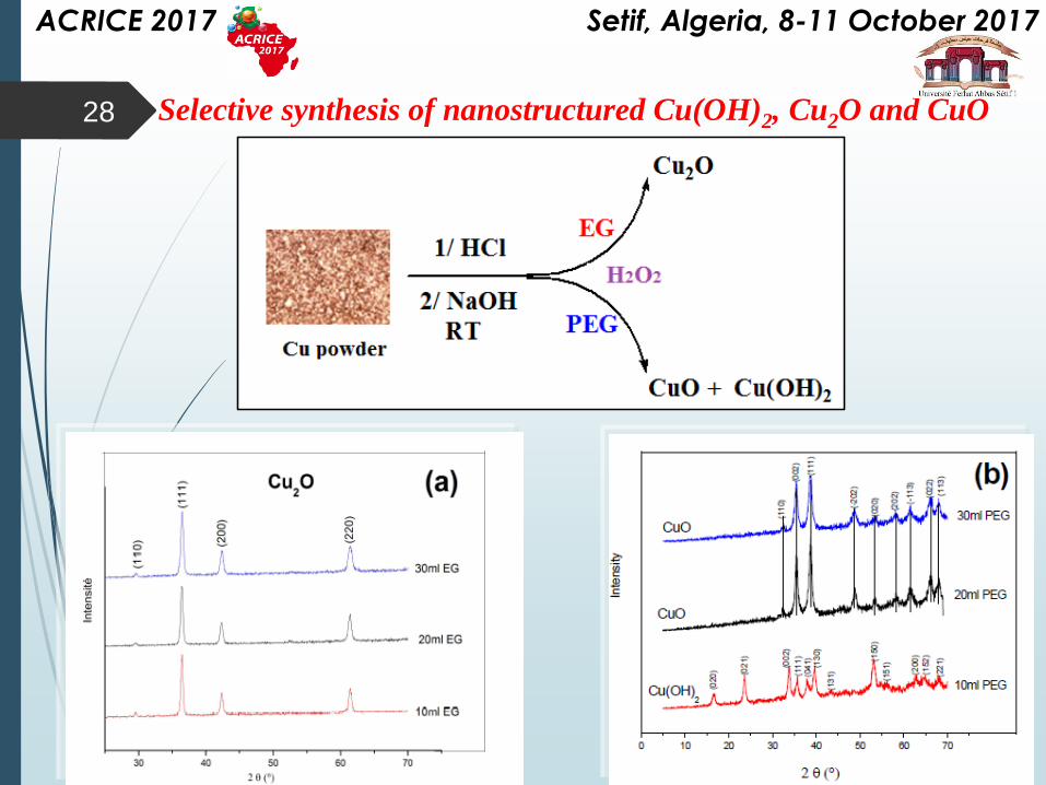
28 Selective synthesis of nanostructured Cu(OH)2, Cu2O and CuO
ACRICE 2017 Setif, Algeria, 8-11 October 2017
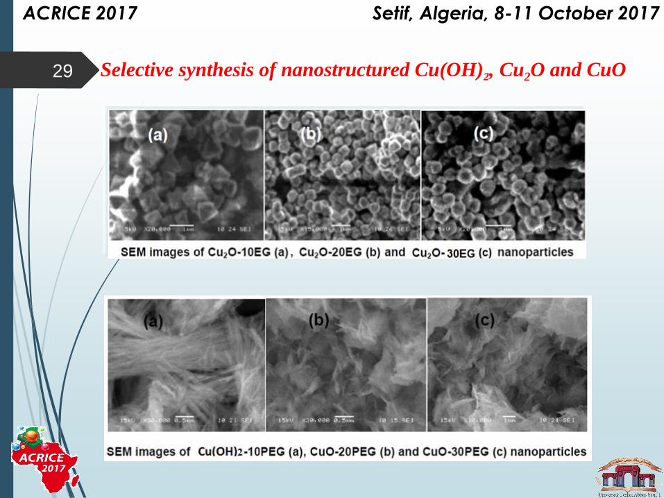
29 Selective synthesis of nanostructured Cu(OH)2, Cu2O and CuO
ACRICE 2017 Setif, Algeria, 8-11 October 2017
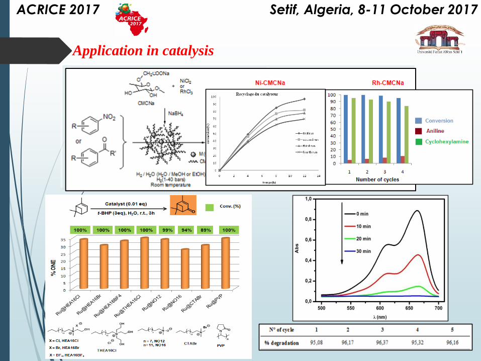
Nitro- and ceto-aromatic reduction
Treatment of Wastewater: Methylene Blue degradation
CuO(Np) Or ZnO(Np)
Terpene oxidation: Ru(Np)
Application in catalysis
ACRICE 2017 Setif, Algeria, 8-11 October 2017
31 Outline
✓ 2D Materials:
o Silicon nanosheets (SiNSs) and silicene
o Black phosphorus and phosphorene
✓ Conclusion
ACRICE 2017 Setif, Algeria, 8-11 October 2017
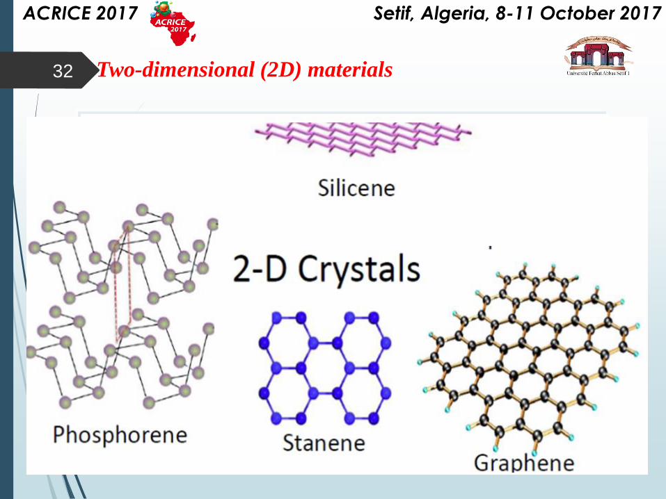
32
There are several categories which are classified as follows:
Their extraordinarily high specific surface area makes them
promising candidates for a variety of applications in
nanotechnology.
Two-dimensional (2D) materials
ACRICE 2017 Setif, Algeria, 8-11 October 2017
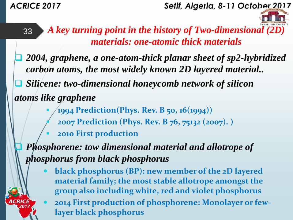
2004, graphene, a one-atom-thick planar sheet of sp2-hybridized
carbon atoms, the most widely known 2D layered material..
Silicene: two-dimensional honeycomb network of silicon
atoms like graphene
▪ 1994 Prediction(Phys. Rev. B 50, 16(1994))
▪ 2007 Prediction (Phys. Rev. B 76, 75132 (2007). )
▪ 2010 First production
Phosphorene: tow dimensional material and allotrope of
phosphorus from black phosphorus
black phosphorus (BP): new member of the 2D layered material family; the most stable allotrope amongst the group also including white, red and violet phosphorus
2014 First production of phosphorene: Monolayer or few-layer black phosphorus
A key turning point in the history of Two-dimensional (2D)
materials: one-atomic thick materials33
ACRICE 2017 Setif, Algeria, 8-11 October 2017
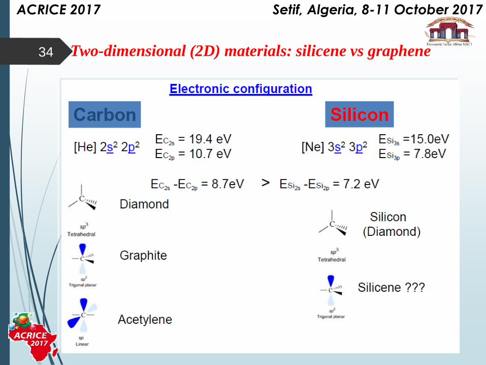
34 Two-dimensional (2D) materials: silicene vs graphene
ACRICE 2017 Setif, Algeria, 8-11 October 2017
35 Outline
✓ Introduction
✓ Chemical Approaches to 2D Materials
o Chemical exfoliation of 2D materials
o Stabilization modes of exfoliated 2D materials
✓ Silicon nanosheets (SiNSs): Synthesis methods
✓ Liquid-phase exfoliation of calcium disilicide
✓ Recent Advances in Silicon sheets
✓ Black phosphorus Synthesis
✓ Conclusion
ACRICE 2017 Setif, Algeria, 8-11 October 2017
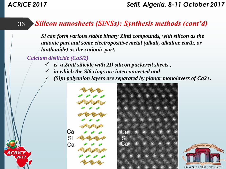
Si can form various stable binary Zintl compounds, with silicon as the
anionic part and some electropositive metal (alkali, alkaline earth, or
lanthanide) as the cationic part.
Calcium disilicide (CaSi2)
✓ is a Zintl silicide with 2D silicon puckered sheets ,
✓ in which the Si6 rings are interconnected and
✓ (Si)n polyanion layers are separated by planar monolayers of Ca2+.
36 Silicon nanosheets (SiNSs): Synthesis methods (cont’d)
ACRICE 2017 Setif, Algeria, 8-11 October 2017
37
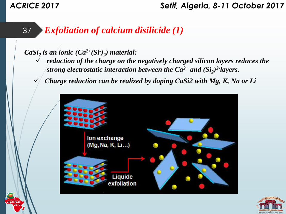
CaSi2 is an ionic (Ca2+(Si-)2) material:
✓ reduction of the charge on the negatively charged silicon layers reduces the
strong electrostatic interaction between the Ca2+ and (Si2)2-layers.
Exfoliation of calcium disilicide (1)
✓ Charge reduction can be realized by doping CaSi2 with Mg, K, Na or Li
ACRICE 2017 Setif, Algeria, 8-11 October 2017
H. Nakano, et al. Angew. Chem. 2006, 118, 6451 – 6454; Angew. Chem. Int. Ed. 2006, 45, 6303 – 6306.
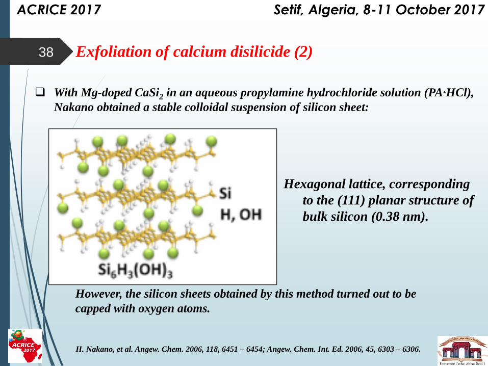
Exfoliation of calcium disilicide (2)
With Mg-doped CaSi2 in an aqueous propylamine hydrochloride solution (PA·HCl),
Nakano obtained a stable colloidal suspension of silicon sheet:
38
Hexagonal lattice, corresponding
to the (111) planar structure of
bulk silicon (0.38 nm).
However, the silicon sheets obtained by this method turned out to be
capped with oxygen atoms.
ACRICE 2017 Setif, Algeria, 8-11 October 2017
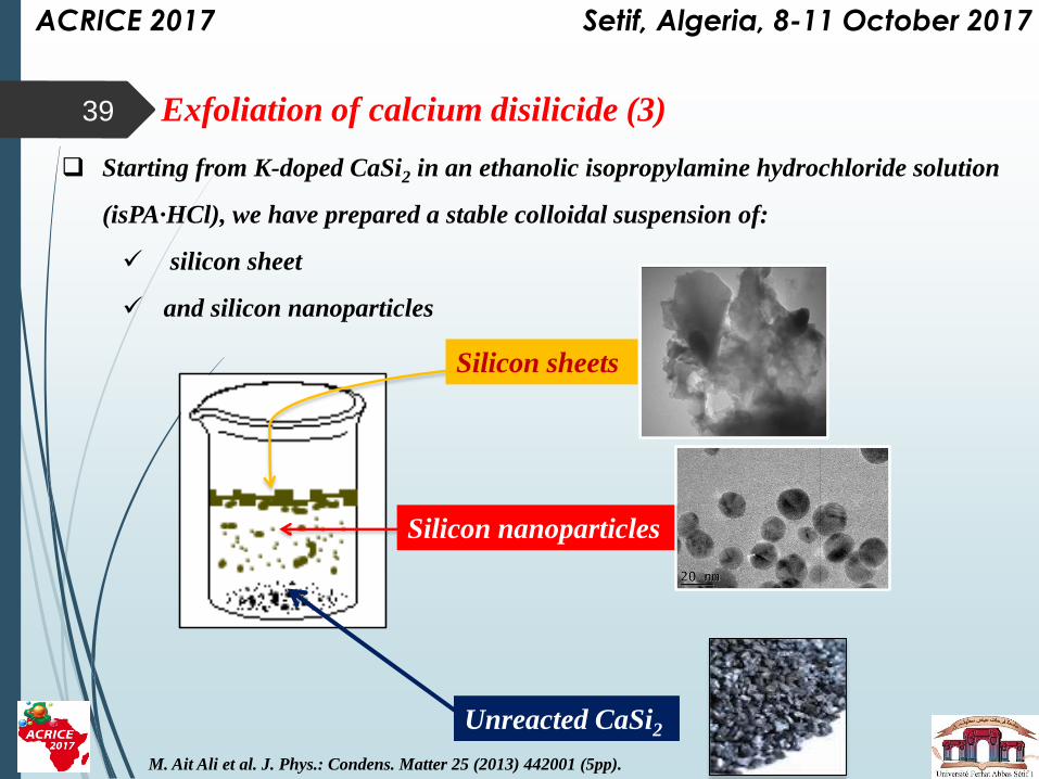
Silicon sheets
Silicon nanoparticles
39
Unreacted CaSi2
Exfoliation of calcium disilicide (3)
Starting from K-doped CaSi2 in an ethanolic isopropylamine hydrochloride solution
(isPA·HCl), we have prepared a stable colloidal suspension of:
✓ silicon sheet
✓ and silicon nanoparticles
ACRICE 2017 Setif, Algeria, 8-11 October 2017
M. Ait Ali et al. J. Phys.: Condens. Matter 25 (2013) 442001 (5pp).
40
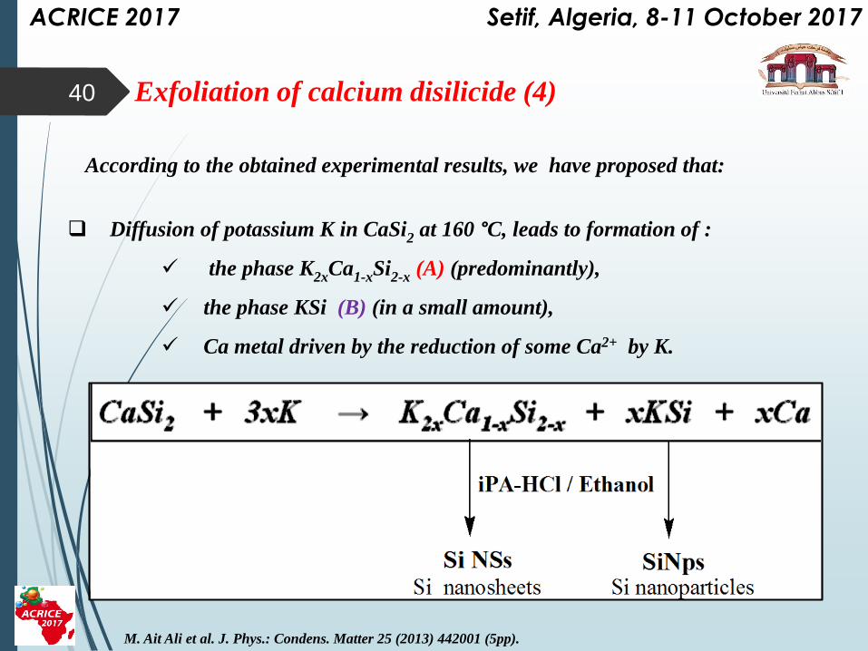
Diffusion of potassium K in CaSi2 at 160 °C, leads to formation of :
✓ the phase K2xCa1-xSi2-x (A) (predominantly),
✓ the phase KSi (B) (in a small amount),
✓ Ca metal driven by the reduction of some Ca2+ by K.
According to the obtained experimental results, we have proposed that:
Exfoliation of calcium disilicide (4)
ACRICE 2017 Setif, Algeria, 8-11 October 2017
M. Ait Ali et al. J. Phys.: Condens. Matter 25 (2013) 442001 (5pp).
M. Ait Ali et al. J. Phys.: Condens. Matter 25 (2013) 442001 (5pp).
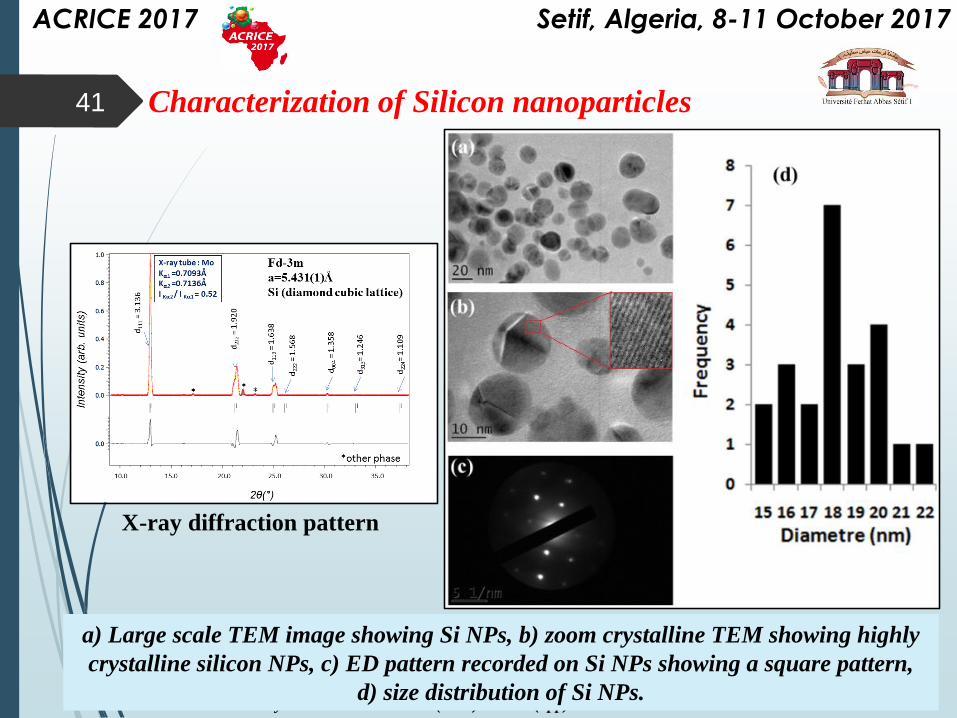
X-ray diffraction pattern
Characterization of Silicon nanoparticles41
a) Large scale TEM image showing Si NPs, b) zoom crystalline TEM showing highly
crystalline silicon NPs, c) ED pattern recorded on Si NPs showing a square pattern,
d) size distribution of Si NPs.
ACRICE 2017 Setif, Algeria, 8-11 October 2017
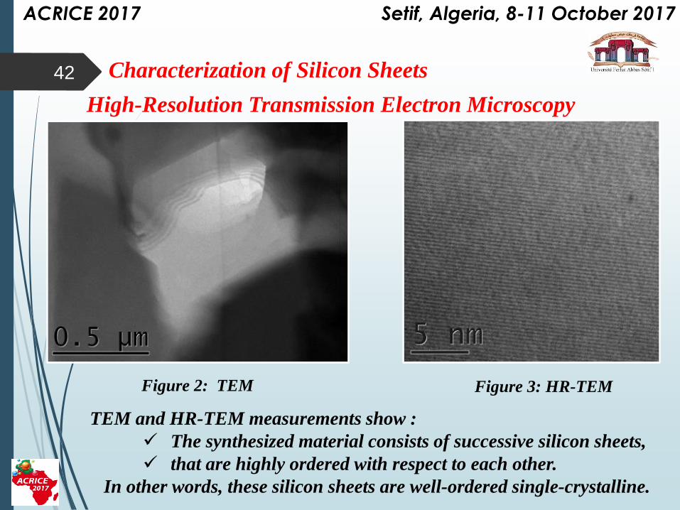
High-Resolution Transmission Electron Microscopy
Characterization of Silicon Sheets
TEM and HR-TEM measurements show :
✓ The synthesized material consists of successive silicon sheets,
✓ that are highly ordered with respect to each other.
In other words, these silicon sheets are well-ordered single-crystalline.
Figure 2: TEM Figure 3: HR-TEM
42
ACRICE 2017 Setif, Algeria, 8-11 October 2017
Characterization of Silicon Sheets (2)
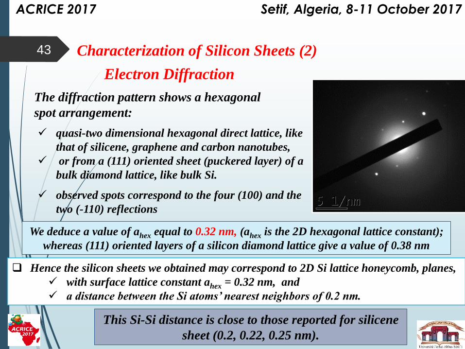
Electron Diffraction
The diffraction pattern shows a hexagonal
spot arrangement:
✓ quasi-two dimensional hexagonal direct lattice, like
that of silicene, graphene and carbon nanotubes,
✓ or from a (111) oriented sheet (puckered layer) of a
bulk diamond lattice, like bulk Si.
✓ observed spots correspond to the four (100) and the
two (-110) reflections
We deduce a value of ahex equal to 0.32 nm, (ahex is the 2D hexagonal lattice constant);
whereas (111) oriented layers of a silicon diamond lattice give a value of 0.38 nm
43
ACRICE 2017 Setif, Algeria, 8-11 October 2017
Hence the silicon sheets we obtained may correspond to 2D Si lattice honeycomb, planes,
✓ with surface lattice constant ahex = 0.32 nm, and
✓ a distance between the Si atoms’ nearest neighbors of 0.2 nm.
This Si-Si distance is close to those reported for silicene
sheet (0.2, 0.22, 0.25 nm).
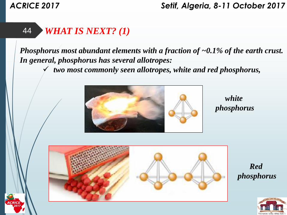
44 WHAT IS NEXT? (1)
Phosphorus most abundant elements with a fraction of ~0.1% of the earth crust.
In general, phosphorus has several allotropes:
✓ two most commonly seen allotropes, white and red phosphorus,
white
phosphorus
Red
phosphorus
ACRICE 2017 Setif, Algeria, 8-11 October 2017
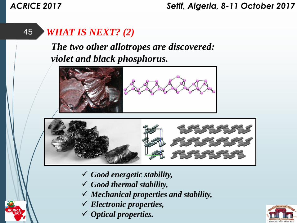
45 WHAT IS NEXT? (2)
The two other allotropes are discovered:
violet and black phosphorus.
✓ Good energetic stability,
✓ Good thermal stability,
✓ Mechanical properties and stability,
✓ Electronic properties,
✓ Optical properties.
ACRICE 2017 Setif, Algeria, 8-11 October 2017
46
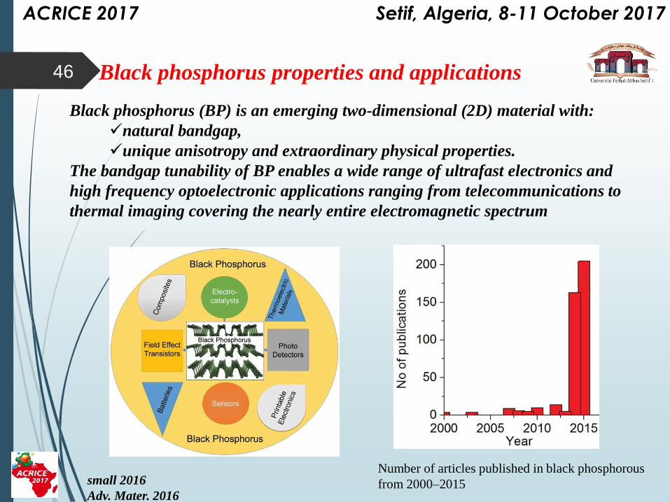
Black phosphorus (BP) is an emerging two-dimensional (2D) material with:
✓natural bandgap,
✓unique anisotropy and extraordinary physical properties.
The bandgap tunability of BP enables a wide range of ultrafast electronics and
high frequency optoelectronic applications ranging from telecommunications to
thermal imaging covering the nearly entire electromagnetic spectrum
Number of articles published in black phosphorous
from 2000–2015small 2016
Adv. Mater. 2016
Black phosphorus properties and applications
ACRICE 2017 Setif, Algeria, 8-11 October 2017
47
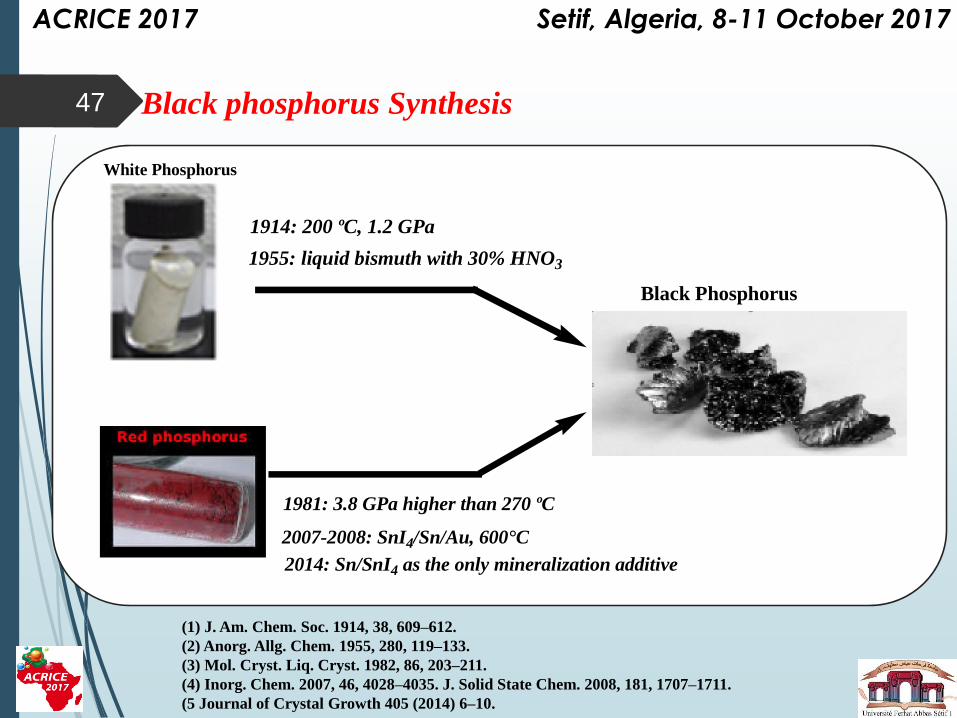
(1) J. Am. Chem. Soc. 1914, 38, 609–612.
(2) Anorg. Allg. Chem. 1955, 280, 119–133.
(3) Mol. Cryst. Liq. Cryst. 1982, 86, 203–211.
(4) Inorg. Chem. 2007, 46, 4028–4035. J. Solid State Chem. 2008, 181, 1707–1711.
(5 Journal of Crystal Growth 405 (2014) 6–10.
Black phosphorus Synthesis
1981: 3.8 GPa higher than 270 ºC
2007-2008: SnI4/Sn/Au, 600°C
2014: Sn/SnI4 as the only mineralization additive
Black Phosphorus
1914: 200 ºC, 1.2 GPa
1955: liquid bismuth with 30% HNO3
White Phosphorus
ACRICE 2017 Setif, Algeria, 8-11 October 2017
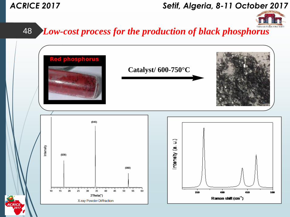
48 Low-cost process for the production of black phosphorus
Catalyst/ 600-750°C
ACRICE 2017 Setif, Algeria, 8-11 October 2017
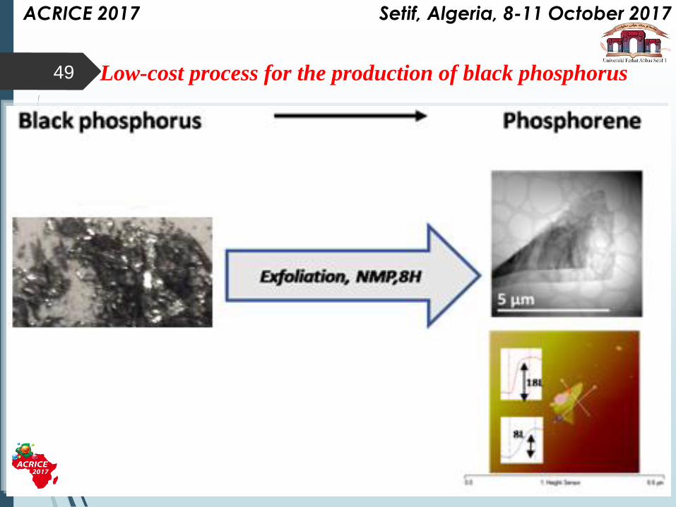
49
Scanning Microscopy Electron, EDX Analysis HR-TEM
Low-cost process for the production of black phosphorus
ACRICE 2017 Setif, Algeria, 8-11 October 2017
Conclusion50
Chemical synthesis of nanomaterials is one of the important method .
So, mastering the chemical approach is a major contribution to the progress of the science
and technology of nanomaterials, fostering the invention of new up-scalable methods for
there production.
Overall, the real evolution of nanomaterials technology will depend on how effectively
we will be able to face the challenges in:
✓ production,
✓ processing,
✓ and chemical tunability.
ACRICE 2017 Setif, Algeria, 8-11 October 2017
2D-systems confined in two dimensions as Si and P nanosheets.
Their extraordinarily high specific surface area and their specific properties makes them a
promising candidates for a variety of applications in nanotechnology
We believe that the chemical approaches shall help to translate 2D
nanomaterials from the laboratory into a real, high-impact technology.
Acknowledgement:
Dr. Omar MOUNKACHI
Pr. Mohamed HAMEDOUN
Pr. Abdelillah BENYOUSSEF
Dr. Abdelfattah MAHMOUD
Dr. Frederic BOSCHINI
Pr. Mustapha AIT ALI
Pr. Abdessadek LACHGAR
Dr. Dris IHIAWAKRIM
PR. Ovidiu ERSEN
Pr. Hamid OUGHADDOU
Pr.Abdelkader KARA
ACRICE 2017 Setif, Algeria, 8-11 October 2017
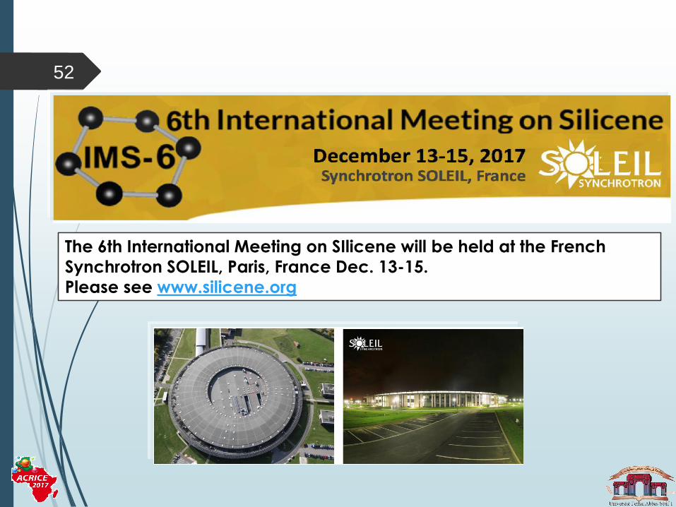
52
The 6th International Meeting on SIlicene will be held at the French
Synchrotron SOLEIL, Paris, France Dec. 13-15.
Please see www.silicene.org