Embed Size (px)
Citation preview
LM3253
www.ti.com SNVS791Q –FEBRUARY 2012–REVISED MAY 2013
LM3253 High-Current Step-Down Converter for 2G/3G/4G RF Power AmplifiersCheck for Samples: LM3253
1FEATURES2• High-Efficiency PFM and PWM Modes with DESCRIPTION
Internal Synchronous Rectification The LM3253 is a DC-DC converter optimized forpowering multi-mode 2G/3G/4G RF power amplifiers• Analog Bypass Function with Low Dropout(PAs) from a single Lithium-Ion cell. The LM3253Resistance (45 mΩ typ.)steps down an input voltage from 2.7V to 5.5V to a
• Dynamically Adjustable Output Voltage, 0.4V dynamically adjustable output voltage of 0.4V to 3.6V.to 3.6V (typ.), in PFM and PWM modes The output voltage is set through a VCON analog
• 3A Maximum Load Current in PWM Mode input that adjusts the output voltage to ensureefficient operation at all power levels of the RF PA.• 2.7MHz (average) PWM Switching FrequencyThe LM3253 is optimized for USB datacard
• Modulated Switching Frequency to Aid Rx applications.Band Compliance
The LM3253 operates in constant frequency Pulse• Operates From a Single Li-ion CellWidth Modulation (PWM) mode producing a small
(2.7V to 5.5V) and predictable amount of output voltage ripple. This• ACB Reduces Inductor Requirements and Size enables best ECTEL power requirements in GMSK
and EDGE spectral compliance, with the minimal• Minimum Total Solution Size by Using Smallamount of filtering and excess headroom. WhenFootprint and Case Size Inductor andoperating in Pulse Frequency Modulation (PFM)Capacitorsmode, the LM3253 enables the lowest DG09 current
• 16-bump Thin DSBGA Package consumption and therefore maximizes system• Current and Thermal Overload Protection efficiency.
The LM3253 has a unique Active Current assist andAPPLICATIONS analog Bypass (ACB) feature to minimize inductorsize without any loss of output regulation for the• USB Datacardsentire battery voltage and RF output power range,• Cellular Phonesuntil dropout. ACB provides a parallel current path,
• Hand-Held Radios when needed, to limit the maximum inductor current• RF PC Cards to 1.84A (typ.) while still driving a 3A load. The ACB
also enables operation with minimal dropout voltage.• Battery-Powered RF DevicesThe LM3253 is available in a small 2 mm x 2 mmchip-scale 16-bump DSBGA package.
When considering the use of the LM3253 in a systemdesign, contact the Texas Instruments Sales or FieldApplication engineer for a copy of the "LM3253:DC-DC Converter for 3G/4G RF PAs PCB LayoutConsiderations.”
1
Please be aware that an important notice concerning availability, standard warranty, and use in critical applications ofTexas Instruments semiconductor products and disclaimers thereto appears at the end of this data sheet.
2All trademarks are the property of their respective owners.
PRODUCTION DATA information is current as of publication date. Copyright © 2012–2013, Texas Instruments IncorporatedProducts conform to specifications per the terms of the TexasInstruments standard warranty. Production processing does notnecessarily include testing of all parameters.

4321
Top View
4 3 2 1
Bottom View
A
B
C
D
A
B
C
D
ACB
ACB
BGND
FB
ACB
ACB
BGND
FB
PVIN
PVIN
BP
MODE
PVIN
PVIN
BP
MODE
SW
SW
EN
VCON
SW
SW
EN
VCON
PGND
PGND
SGND
VDD
PGND
PGND
SGND
VDD
LM3253
PVIN VDDSW
FB
VCON PGND SGND
EN
MODE
VBATT
VOUT
ACB
BP
VCC_PA_2G
BB orRFIC
DAC
GPO2
GPO1
BGND
1.5 µH
10 µF
1.0 µFPA
4.7 µF
PA(s)
VCC_PA_3G
10 µF
LM3253
SNVS791Q –FEBRUARY 2012–REVISED MAY 2013 www.ti.com
Typical System Application Diagram
Connection Diagram
Figure 1. 16-Bump 0.4 mm Pitch Thin DSBGA Package
2 Submit Documentation Feedback Copyright © 2012–2013, Texas Instruments Incorporated
Product Folder Links: LM3253

LM3253
www.ti.com SNVS791Q –FEBRUARY 2012–REVISED MAY 2013
Pin DescriptionsPin # Name Description
A1PGND Power Ground to the internal NFET switch.
B1
C1 SGND Signal Analog and Control Ground (Low Current).
D1 VDD Analog Supply Input.
A2 Switching Node connection to the internal PFET switch and NFET synchronous rectifier. ConnectSW to an inductor with a saturation current rating that exceeds the ILIM,PFET,Steady State Current Limit
B2 specification of the LM3253.
Enable Input. Set this digital input HIGH for normal operation. For shutdown, set low. Pin has anC2 EN 800 kΩ internal pulldown resistor.
D2 VCON Voltage Control Analog input. VOUT = 2.5 x VCON.
A3PVIN Power Supply Voltage Input to the internal PFET switch and ACB.
B3
Bypass Mode Input. Set the pin HIGH for forced Bypass mode operation. Set the pin LOW forC3 BP automatic Analog Bypass Mode (recommended).
PWM/PFM Mode Selection Input. Setting the pin HIGH allows for PFM or PWM, depending onD3 MODE the load current. Setting the pin LOW forces the part to be in PWM only.
A4ACB Analog Current Bypass. Connect to the output at the output filter capacitor.
B4
C4 BGND Active Current assist and analog Bypass Ground (High Current).
D4 FB Feedback Analog Input. Connect to the output at the output filter capacitor.
Copyright © 2012–2013, Texas Instruments Incorporated Submit Documentation Feedback 3
Product Folder Links: LM3253

LM3253
SNVS791Q –FEBRUARY 2012–REVISED MAY 2013 www.ti.com
This integrated circuit can be damaged by ESD. Texas Instruments recommends that all integrated circuits be handled withappropriate precautions. Failure to observe proper handling and installation procedures can cause damage.
ESD damage can range from subtle performance degradation to complete device failure. Precision integrated circuits may be moresusceptible to damage because very small parametric changes could cause the device not to meet its published specifications.
ABSOLUTE MAXIMUM RATINGS (1) (2) (3)
VDD, PVIN to SGND −0.2V to +6.0V
PGND to SGND −0.2V to +0.2V
EN, FB, VCON, BP, MODE (SGND −0.2V) to (VDD +0.2V)
SW, ACB (PGND −0.2V) to (PVIN +0.2V
PVIN to VDD −0.2V to +0.2V
Continuous Power Dissipation (4) Internally Limited
Junction Temperature (TJ-MAX) +150°C
Storage Temperature Range −65°C to +150°C
Maximum Lead Temperature +260°C(Soldering, 10 sec)
ESD Rating (5) (6) Human Body Model 2kV
(1) Stresses beyond those listed under absolute maximum ratings may cause permanent damage to the device. These are stress ratingsonly, and functional operation of the device at these or any other conditions beyond those indicated under recommended operatingconditions is not implied. Exposure to absolute-maximum-rated conditions for extended periods may affect device reliability.
(2) All voltages are with respect to the potential at the GND pins. The LM3253 is designed for mobile phone applications where turn-on afterpower-up is controlled by the system controller and where requirements for a small package size overrule increased die size for internalUnder Voltage Lock-Out (UVLO) circuitry. Thus, it should be kept in shutdown by holding the EN pin LOW until the input voltageexceeds 2.7V.
(3) If Military/Aerospace specified devices are required, please contact the Texas Instruments Sales Office/Distributors for availability andspecifications.
(4) Internal thermal shutdown circuitry protects the device from permanent damage. Thermal shutdown engages at TJ = 150°C (typ.) anddisengages at TJ = 130°C (typ.).
(5) The human body model is a 100 pF capacitor discharged through a 1.5 kΩ resistor into each pin. (MIL-STD-883 3015.7) The machinemodel is a 200 pF capacitor discharged directly into each pin.
(6) Texas Instruments recommends that all integrated circuits be handled with appropriate precautions. Failure to observe proper ESDhandling procedures can result in damage.
4 Submit Documentation Feedback Copyright © 2012–2013, Texas Instruments Incorporated
Product Folder Links: LM3253

LM3253
www.ti.com SNVS791Q –FEBRUARY 2012–REVISED MAY 2013
OPERATING RATINGS (1)
Input Voltage Range 2.7V to 5.5V
Recommended Load Current 0A to 3.0A
Junction Temperature (TJ) Range −30°C to +125°C
Ambient Temperature (TA) Range (2) −30°C to +90°C
(1) All voltages are with respect to the potential at the GND pins. The LM3253 is designed for mobile phone applications where turn-on afterpower-up is controlled by the system controller and where requirements for a small package size overrule increased die size for internalUnder Voltage Lock-Out (UVLO) circuitry. Thus, it should be kept in shutdown by holding the EN pin LOW until the input voltageexceeds 2.7V.
(2) In applications where high-power dissipation and/or poor package thermal resistance is present, the maximum ambient temperature mayhave to be de-rated. Maximum ambient temperature (TA-MAX) is dependent on the maximum operating junction temperature (TJ-MAX-OP =125°C), the maximum power dissipation of the device in the application (PD-MAX), and the junction-to ambient thermal resistance of thepart/package in the application (θJA), as given by the following equation: TA-MAX = TJ-MAX-OP – (θJA × PD-MAX). At higher power levels dutycycle usage is assumed to drop (i.e., max power 12.5% usage is assumed) for 2G mode.
THERMAL PROPERTIESJunction-to-Ambient Thermal 50°C/W
Resistance (θJA), YFQ Package (1)
(1) Junction-to-ambient thermal resistance (θJA) is taken from thermal modeling result, performed under the conditions and guidelines setforth in the JEDEC standard JESD51-7.
Copyright © 2012–2013, Texas Instruments Incorporated Submit Documentation Feedback 5
Product Folder Links: LM3253
LM3253
SNVS791Q –FEBRUARY 2012–REVISED MAY 2013 www.ti.com
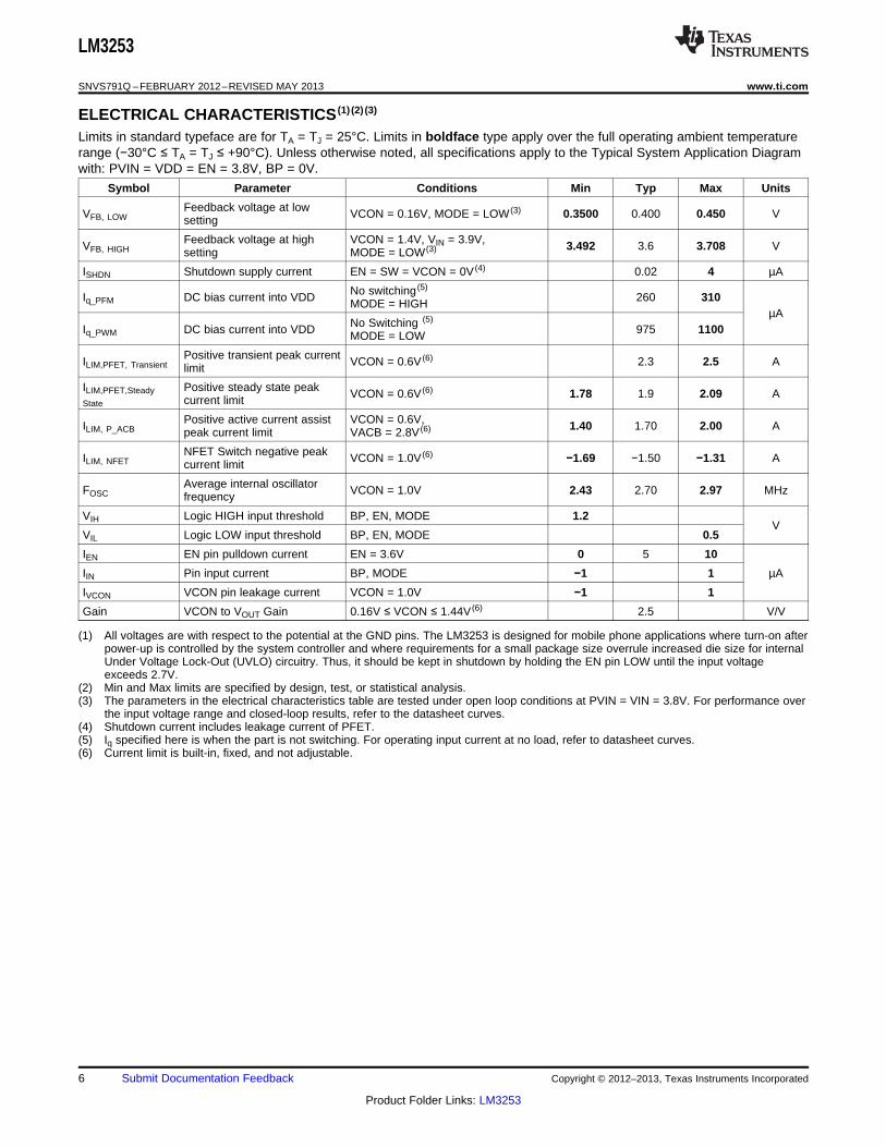
ELECTRICAL CHARACTERISTICS (1) (2) (3)
Limits in standard typeface are for TA = TJ = 25°C. Limits in boldface type apply over the full operating ambient temperaturerange (−30°C ≤ TA = TJ ≤ +90°C). Unless otherwise noted, all specifications apply to the Typical System Application Diagramwith: PVIN = VDD = EN = 3.8V, BP = 0V.
Symbol Parameter Conditions Min Typ Max Units
Feedback voltage at lowVFB, LOW VCON = 0.16V, MODE = LOW (3) 0.3500 0.400 0.450 Vsetting
Feedback voltage at high VCON = 1.4V, VIN = 3.9V,VFB, HIGH 3.492 3.6 3.708 Vsetting MODE = LOW (3)
ISHDN Shutdown supply current EN = SW = VCON = 0V (4) 0.02 4 µA
No switching (5)Iq_PFM DC bias current into VDD 260 310MODE = HIGH
µANo Switching (5)
Iq_PWM DC bias current into VDD 975 1100MODE = LOW
Positive transient peak currentILIM,PFET, Transient VCON = 0.6V (6) 2.3 2.5 Alimit
ILIM,PFET,Steady Positive steady state peak VCON = 0.6V (6) 1.78 1.9 2.09 AState current limit
Positive active current assist VCON = 0.6V,ILIM, P_ACB 1.40 1.70 2.00 Apeak current limit VACB = 2.8V (6)
NFET Switch negative peakILIM, NFET VCON = 1.0V (6) −1.69 −1.50 −1.31 Acurrent limit
Average internal oscillatorFOSC VCON = 1.0V 2.43 2.70 2.97 MHzfrequency
VIH Logic HIGH input threshold BP, EN, MODE 1.2V
VIL Logic LOW input threshold BP, EN, MODE 0.5
IEN EN pin pulldown current EN = 3.6V 0 5 10
IIN Pin input current BP, MODE −1 1 µA
IVCON VCON pin leakage current VCON = 1.0V −1 1
Gain VCON to VOUT Gain 0.16V ≤ VCON ≤ 1.44V (6) 2.5 V/V
(1) All voltages are with respect to the potential at the GND pins. The LM3253 is designed for mobile phone applications where turn-on afterpower-up is controlled by the system controller and where requirements for a small package size overrule increased die size for internalUnder Voltage Lock-Out (UVLO) circuitry. Thus, it should be kept in shutdown by holding the EN pin LOW until the input voltageexceeds 2.7V.
(2) Min and Max limits are specified by design, test, or statistical analysis.(3) The parameters in the electrical characteristics table are tested under open loop conditions at PVIN = VIN = 3.8V. For performance over
the input voltage range and closed-loop results, refer to the datasheet curves.(4) Shutdown current includes leakage current of PFET.(5) Iq specified here is when the part is not switching. For operating input current at no load, refer to datasheet curves.(6) Current limit is built-in, fixed, and not adjustable.
6 Submit Documentation Feedback Copyright © 2012–2013, Texas Instruments Incorporated
Product Folder Links: LM3253
LM3253
www.ti.com SNVS791Q –FEBRUARY 2012–REVISED MAY 2013
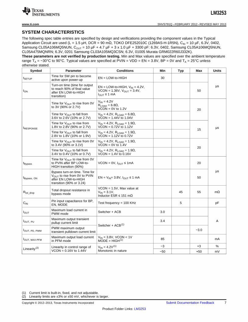
SYSTEM CHARACTERISTICSThe following spec table entries are specified by design and verifications providing the component values in the TypicalApplication Circuit are used (L = 1.5 µH, DCR = 90 mΩ, TOKO DFE252010C (1269AS-H-1R5N), CIN = 10 µF, 6.3V, 0402,Samsung CL05A106MQ5NUN, COUT = 10 µF + 4.7 µF + 3 x 1.0 µF + 3300 pF: 6.3V, 0402, Samsung CL05A106MQ5NUN,CL05A475MQNRN; 6.3V, 0201 Samsung CL03A105MQ3CSN; 6.3V, 01005 Murata GRM022R60J332K).These parameters are not verified by production testing. Min and Max values are specified over the ambient temperaturerange TA = −30°C to 90°C. Typical values are specified at PVIN = VDD = EN = 3.8V, BP = 0V and TA = 25°C unlessotherwise stated.
Symbol Parameter Conditions Min Typ Max Units
Time for SW pin to becometSETUP EN = LOW-to-HIGH 30active upon power-up
Turn-on time (time for output µsEN = LOW-to-HIGH, VIN = 4.2V,to reach 90% of final valuetON VCON = 1.36V, VOUT = 3.4V, 50after EN LOW-to-HIGH IOUT ≤ 1 mAtransition)
VIN = 4.2VTime for VOUT to rise from 0V RLOAD = 6.8Ω,to 3V (90% or 2.7V) VCON = 0V to 1.2V 20Time for VOUT to fall from VIN = 4.2V, RLOAD = 6.8Ω,3.6V to 2.6V (10% or 2.7V) VCON = 1.44V to 1.04V
Time for VOUT to rise from VIN = 4.2V, RLOAD = 1.9Ω,1.8V to 2.8V (90% or 2.7V) VCON = 0.72V to 1.12VtRESPONSE µs15Time for VOUT to fall from VIN = 4.2V, RLOAD = 1.9Ω,2.8V to 1.8V (10% or 1.9V) VCON = 1.12V to 0.72V
Time for VOUT to rise from 0V VIN = 4.2V, RLOAD = 1.9Ω,to 3.4V (90% or 3.1V) VCON = 0V to 1.4V
20Time for VOUT to fall from VIN = 4.2V, RLOAD = 1.9Ω,3.4V to 0.4V (10% or 0.7V) VCON = 1.4V to 0.16V
Time for VOUT to rise from 0VtBypass to PVIN after BP LOW-to- VCON = 0V, IOUT ≤ 1mA 20
HIGH transition (90%)µsBypass turn-on time. Time for
VOUT to rise from 0V to PVINtBypass, ON EN = VIN= 3.8V, IOUT ≤ 1 mA 50after EN LOW-to-HIGHtransition (90% or 3.24)
VCON = 1.5V, Max value atTotal dropout resistance inRtot_drop VIN = 3.1V, 45 55 mΩbypass mode Inductor ESR ≤ 151 mΩPin input capacitance for BP,CIN Test frequency = 100 KHz 5 pFEN, MODE
Maximum load current inIOUT Switcher + ACB 3.0PWM mode
Maximum output transientIOUT, PU 3.4 Apullup current limitSwitcher + ACB (1)
PWM maximum outputIOUT, PD, PWM −3.0transient pulldown current limit
Maximum output load current VIN = 3.8V, VCON < 1VIOUT, MAX-PFM 85 mAin PFM mode MODE = HIGH (1)
−3 +3 %Linearity in control range of VIN = 4.2V (1)Linearity (2)
VCON = 0.16V to 1.44V Monotonic in nature −50 +50 mV
(1) Current limit is built-in, fixed, and not adjustable.(2) Linearity limits are ±3% or ±50 mV, whichever is larger.
Copyright © 2012–2013, Texas Instruments Incorporated Submit Documentation Feedback 7
Product Folder Links: LM3253

LM3253
SNVS791Q –FEBRUARY 2012–REVISED MAY 2013 www.ti.com
SYSTEM CHARACTERISTICS (continued)The following spec table entries are specified by design and verifications providing the component values in the TypicalApplication Circuit are used (L = 1.5 µH, DCR = 90 mΩ, TOKO DFE252010C (1269AS-H-1R5N), CIN = 10 µF, 6.3V, 0402,Samsung CL05A106MQ5NUN, COUT = 10 µF + 4.7 µF + 3 x 1.0 µF + 3300 pF: 6.3V, 0402, Samsung CL05A106MQ5NUN,CL05A475MQNRN; 6.3V, 0201 Samsung CL03A105MQ3CSN; 6.3V, 01005 Murata GRM022R60J332K).These parameters are not verified by production testing. Min and Max values are specified over the ambient temperaturerange TA = −30°C to 90°C. Typical values are specified at PVIN = VDD = EN = 3.8V, BP = 0V and TA = 25°C unlessotherwise stated.
Symbol Parameter Conditions Min Typ Max Units
VIN = 3.8V, VOUT = 1.8V,IOUT = 10 mA 79 82MODE = HIGH (PFM)
VIN = 3.8V, VOUT = 0.5V,IOUT = 5 mA 58 60MODE = HIGH (PFM)
VIN = 3.8V, VOUT = 3.5V,IOUT = 1900 mA 89 92MODE = LOW (PWM)
η Efficiency %VIN = 3.8V, VOUT = 2.5V,IOUT = 250 mA 90 93MODE = LOW (PWM)
VIN = 3.8V, VOUT = 1.6V,IOUT = 130 mA 83 86MODE = LOW (PWM)
VIN = 3.8V, VOUT = 1V,IOUT = 400 mA 81 84MODE = LOW (PWM)
VIN = 3.4V to 3.6V, VOUT = 0.4V toRipple voltage at no pulse 3.6V, ROUT = 1.9Ω (3) 1 3skipping condition MODE = LOW
Ripple voltage at pulse VIN = 5.5V to dropout, VOUT = 3.6V, 8skipping condition ROUT = 1.9Ω (3)VRIPPLE mVpp
VIN = 3.2V, VOUT < 1.125V, 50IOUT =10 mA, MODE = HIGHPFM Ripple Voltage
VIN = 3.2V, VOUT ≤ 0.5V, 50IOUT = 5 mA, MODE = LOW
VIN = 3.6V to 4.2V, TR = TF = 10 µs,Line_tr Line transient response VOUT = 1V, IOUT = 600 mA 50 mVpk
MODE = LOW
VOUT = 3.0V, TR = TF = 10 µs,Load_tr Load transient response IOUT = 0A to 1.2A 40 mVpk
MODE = LOW
Max Duty cycle Maximum duty cycle MODE = LOW 100 %
VIN = 3.2V, VOUT = 1V, IOUT = 10 mA 100 160MODE = HIGHPFM_Freq Minimum PFM Frequency kHz
VIN = 3.2V, VOUT = 0.5V, IOUT = 5 mA 34 55MODE = HIGH
(3) Ripple voltage should be measured at COUT electrode on a well-designed PC board and using the suggested inductor and capacitors.
8 Submit Documentation Feedback Copyright © 2012–2013, Texas Instruments Incorporated
Product Folder Links: LM3253
2.5 3.0 3.5 4.0 4.5 5.0 5.52.4
2.6
2.8
3.0
3.2
3.4
3.6
OU
TP
UT
VO
LTA
GE
(V
)
INPUT VOLTAGE (V)
DROPOUT
IOUT= 1.5A
0.0 0.2 0.4 0.6 0.8 1.0 1.2 1.4 1.6
0.0
0.5
1.0
1.5
2.0
2.5
3.0
3.5
4.0
OU
TP
UT
VO
LTA
GE
(V
)
VCON (V)
2.5X GAIN
0 200 400 600 800 1000
70
75
80
85
90
95
100
EF
FIC
IEN
CY
(%
)
LOAD CURRENT (mA)
VOUT = 1.6VVOUT = 2.0VVOUT = 2.5VVOUT = 3.0VVOUT = 3.5V
900 1200 1500 1800 2100 2400 2700
0
10
20
30
40
50
60
70
80
90
100
EF
FIC
IEN
CY
(%
)
LOAD CURRENT (mA)
VOUT = 2.0VVOUT = 2.5VVOUT = 3.0VVOUT = 3.5V
0 20 40 60 80 100 120 140 160
60
65
70
75
80
85
90
95
100
EF
FIC
IEN
CY
(%
)
LOAD CURRENT (mA)
VOUT = 1.0VVOUT = 1.5VVOUT = 2.0VVOUT = 2.5VVOUT = 3.0V
0 100 200 300 400 500 600 700 800
60
65
70
75
80
85
90
95
100
EF
FIC
EN
CY
(%
)
LOAD CURRENT (mA)
VOUT = 1.6VVOUT = 2.0VVOUT = 2.5VVOUT = 3.0VVOUT = 3.5V
LM3253
www.ti.com SNVS791Q –FEBRUARY 2012–REVISED MAY 2013
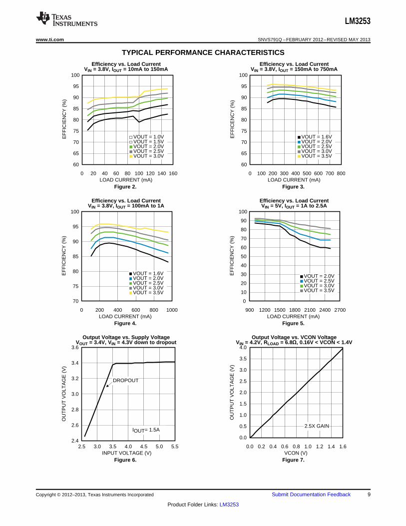
TYPICAL PERFORMANCE CHARACTERISTICS
Efficiency vs. Load Current Efficiency vs. Load CurrentVIN = 3.8V, IOUT = 10mA to 150mA VIN = 3.8V, IOUT = 150mA to 750mA
Figure 2. Figure 3.
Efficiency vs. Load Current Efficiency vs. Load CurrentVIN = 3.8V, IOUT = 100mA to 1A VIN = 5V, IOUT = 1A to 2.5A
Figure 4. Figure 5.
Output Voltage vs. Supply Voltage Output Voltage vs. VCON VoltageVOUT = 3.4V, VIN = 4.3V down to dropout VIN = 4.2V, RLOAD = 6.8Ω, 0.16V < VCON < 1.4V
Figure 6. Figure 7.
Copyright © 2012–2013, Texas Instruments Incorporated Submit Documentation Feedback 9
Product Folder Links: LM3253

20 s/DIV
IOUT
2V/DIV
1A/DIV
VCON 2V/DIV
VOUT
20 s/DIV
5 mV/DIVVOUT
50 mA/DIVIOUT
2.5 3.0 3.5 4.0 4.5 5.0 5.5 6.0
0
2
4
6
8
10
12
QU
IES
CE
NT
CU
RR
EN
T (
mA
)
INPUT VOLTAGE (V)
20 s/DIV
IOUT
2V/DIV
500 mA/DIV
VCON 2V/DIV
VOUT
3.0 3.5 4.0 4.5 5.0 5.5 6.0
2.50
2.55
2.60
2.65
2.70
2.75
2.80
2.85
2.90
2.95
3.00S
WIT
CH
ING
FR
EQ
UE
NC
Y (
MH
z)
INPUT VOLTAGE (V)2.5 3.0 3.5 4.0 4.5 5.0 5.5 6.0
210
220
230
240
250
260
270
280
290
QU
IES
CE
NT
CU
RR
EN
T (
A)
INPUT VOLTAGE (V)
LM3253
SNVS791Q –FEBRUARY 2012–REVISED MAY 2013 www.ti.com
TYPICAL PERFORMANCE CHARACTERISTICS (continued)Center-Switching Frequency vs. Supply Voltage Quiescent Current (PFM) vs. Supply Voltage
VOUT = 2.5V, IOUT = 700mA, VIN = 3.8V VOUT = 1V, 2.7V < VIN< 5.5V (No Load)
Figure 8. Figure 9.
Quiescent Current (PWM) vs. Supply Voltage VCON Transient (3G/4G)VOUT = 2.5V, 2.7V < VIN< 5.5V (No Load) VOUT = 0V to 3V, RLOAD = 6.8Ω, VIN = 3.8V
Figure 10. Figure 11.
VCON Transient (2G) Load Transient in PFM ModeVOUT = 1.4V to 3.4V, RLOAD = 1.9Ω, VIN = 4.2V VOUT = 1V, IOUT = 0mA to 60mA, VIN = 3.6V
Figure 12. Figure 13.
10 Submit Documentation Feedback Copyright © 2012–2013, Texas Instruments Incorporated
Product Folder Links: LM3253
100 s/DIV
50 mV/DIVVOUT
1V/DIVVIN
20 s/DIV
2V/DIV
VOUT
1V/DIV
VSW
2V/DIV
EN
100 Ps/DIV
100 mV/DIVVOUT
IOUT500 mA/DIV
100 s/DIV
50 mV/DIVVOUT
1V/DIVVIN
100 Ps/DIV
20 mV/DIVVOUT
200 mA/DIV
IOUT
100 Ps/DIV
50 mV/DIVVOUT
500 mA/DIVIOUT
LM3253
www.ti.com SNVS791Q –FEBRUARY 2012–REVISED MAY 2013
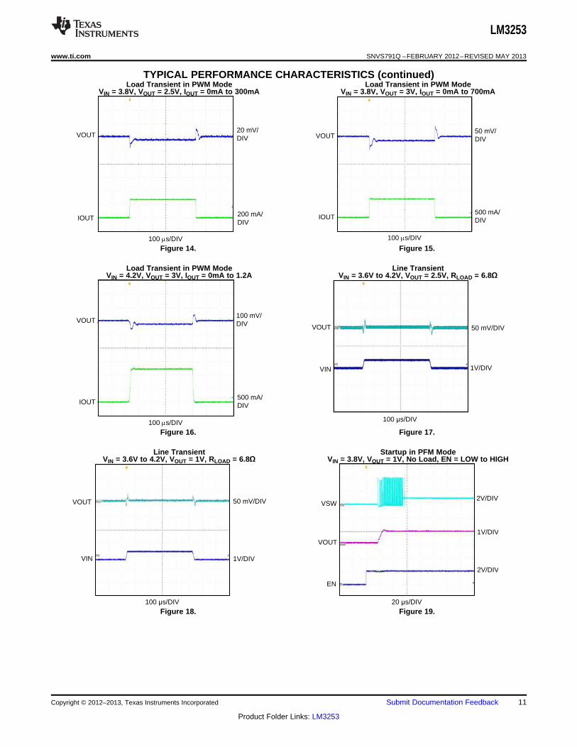
TYPICAL PERFORMANCE CHARACTERISTICS (continued)Load Transient in PWM Mode Load Transient in PWM Mode
VIN = 3.8V, VOUT = 2.5V, IOUT = 0mA to 300mA VIN = 3.8V, VOUT = 3V, IOUT = 0mA to 700mA
Figure 14. Figure 15.
Load Transient in PWM Mode Line TransientVIN = 4.2V, VOUT = 3V, IOUT = 0mA to 1.2A VIN = 3.6V to 4.2V, VOUT = 2.5V, RLOAD = 6.8Ω
Figure 16. Figure 17.
Line Transient Startup in PFM ModeVIN = 3.6V to 4.2V, VOUT = 1V, RLOAD = 6.8Ω VIN = 3.8V, VOUT = 1V, No Load, EN = LOW to HIGH
Figure 18. Figure 19.
Copyright © 2012–2013, Texas Instruments Incorporated Submit Documentation Feedback 11
Product Folder Links: LM3253
20 s/DIV
2V/DIV
VOUT
2V/DIV
VSW
2V/DIV
EN
40 s/DIV
2V/DIV
VOUT
2V/DIVVSW
1A/DIVInductor Current
LM3253
SNVS791Q –FEBRUARY 2012–REVISED MAY 2013 www.ti.com
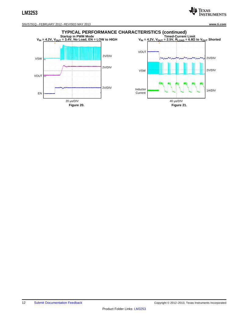
TYPICAL PERFORMANCE CHARACTERISTICS (continued)Startup in PWM Mode Timed-Current Limit
VIN = 4.2V, VOUT = 3.4V, No Load, EN = LOW to HIGH VIN = 4.2V, VOUT = 2.5V, RLOAD = 6.8Ω to VOUT Shorted
Figure 20. Figure 21.
12 Submit Documentation Feedback Copyright © 2012–2013, Texas Instruments Incorporated
Product Folder Links: LM3253
LM3253
www.ti.com SNVS791Q –FEBRUARY 2012–REVISED MAY 2013
OPERATION DESCRIPTION
Device Information
The LM3253 is a high-efficiency step-down DC-DC converter optimized to power the RF power amplifier (PA) incell phones, portable communication devices, or battery-powered RF devices with a single Li-Ion battery. Itoperates in fixed-frequency PWM mode for 2G transmissions (with MODE = LOW), automatic mode transitionbetween PFM and PWM mode for 3G/4G RF PA operation (with MODE = HIGH), forced bypass mode (with BP= HIGH) or in shutdown mode (with EN = LOW).
The fixed-frequency Pulse Width Modulation (PWM) mode provides high efficiency and very low output voltageripple. In Pulse Frequency Modulation (PFM) mode, the converter operates with reduced switching frequenciesand lower supply current to maintain high efficiencies. The forced bypass mode allows the user to drive theoutput directly from the input supply through a bypass FET. The shutdown mode turns the LM3253 off andreduces current consumption to 0.02 µA (typ.).
In PWM and PFM modes of operation, the output voltage of the LM3253 can be dynamically programmed from0.4V to 3.6V (typ.) by adjusting the voltage on VCON. Current overload protection and thermal overloadprotection are also provided.
The LM3253 was engineered with Active Current assist and analog Bypass (ACB). This unique feature allowsthe converter to support maximum load currents of 3A (min.) while keeping a small footprint inductor and meetingall of the transient behaviors required for operation of a multi-mode RF Power Amplifier. The ACB circuit providesan additional current path when the load current exceeds 1.9A (typ.) or as the switcher approaches dropout.Similarly, the ACB circuit allows the converter to respond with faster VCON output voltage transition times byproviding extra output current on rising and falling output edges. The ACB circuit also performs the function ofanalog bypass. Depending upon the input voltage, output voltage and load current, the ACB circuit automaticallyand seamlessly transitions the converter into analog bypass while maintaining output voltage regulation and lowoutput voltage ripple. Full bypass (100% duty cycle operation) will occur if the total dropout resistance in bypassmode (Rtot_drop = 45 mΩ) is insufficient to regulate the output voltage.
The LM3253 16-bump DSBGA package is the best solution for space-constrained applications such as cellphones and other hand-held devices. The high switching frequency, 2.7 MHz (typ.) in PWM mode, reduces thesize of input capacitors, output capacitors and of the inductor. Use of a DSBGA package is best suited foropaque case applications and requires special design considerations for implementation. (Refer to DSBGAPackage Assembly And Use section below). As the LM3253 does not implement UVLO, the system controllershould set EN = LOW and set BP = HIGH during power-up and UVLO conditions. (Refer to Shutdown Modebelow).
PWM Operation
When the LM3253 operates in PWM mode, the switching frequency is constant, and the switcher regulates theoutput voltage by changing the energy-per-cycle to support the load required. During the first portion of eachswitching cycle, the control block in the LM3253 turns on the internal PFET switch. This allows current to flowfrom the input through the inductor and to the output filter capacitor and load. The inductor limits the current to aramp with a slope of (VIN – VOUT)/L, by storing energy in its magnetic field.
During the second portion of each cycle, the control block turns the PFET switch off, blocking current flow fromthe input, and then turns the NFET synchronous rectifier on. The inductor draws current from ground through theNFET and to the output filter capacitor and load, which ramps the inductor current down with a slope of –VOUT/L.The output filter capacitor stores charge when the inductor current is greater than the load current and releases itwhen the inductor current is less than the load current, smoothing the voltage across the load.
At the next rising edge of the clock, the cycle repeats. An increase of load pulls the output voltage down,increasing the error signal. As the error signal increases, the peak inductor current becomes higher, thusincreasing the average inductor current. The output voltage is therefore regulated by modulating the PFET switchon-time to control the average current sent to the load. The circuit generates a duty-cycle modulated rectangularsignal that is averaged using a low pass filter formed by the inductor and output capacitor. The output voltage isequal to the average of the duty-cycle modulated rectangular signal.
Copyright © 2012–2013, Texas Instruments Incorporated Submit Documentation Feedback 13
Product Folder Links: LM3253

LM3253
SNVS791Q –FEBRUARY 2012–REVISED MAY 2013 www.ti.com
PFM Mode
With MODE = HIGH, the LM3253 automatically transitions to from PWM into PFM operation if the averageinductor current is less than 75 mA (typ.) and VIN − VOUT > 0.6V. The switcher regulates the fixed output voltageby transferring a fixed amount of energy during each cycle and modulating the frequency to control the totalpower delivered to the output. The converter switches only as needed to support the demand of the load current,therefore maximizing efficiency. If the load current should increase during PFM mode to more than 95 mA (typ.),the part will automatically transition into constant frequency PWM mode. A 20 mA (typ.) hysteresis window existsbetween PFM and PWM transitions.
After a transient event, the part temporarily operates in 2.7 MHz (typ.) fixed-frequency PWM mode to quicklycharge or discharge the output. This is true for start-up conditions or if MODE pin is toggled LOW-to-HIGH. Oncethe output reaches its target output voltage, and the load is less than 75 mA (typ.), then the part will seamlesslytransition into PFM mode (assuming it is not in forced bypass or auto bypass condition).
Active Current Assist and Analog Bypass (ACB)
The 3GPP time mask requirement for 2G requires high current to be sourced by the LM3253. These highcurrents are required for a small time during transients or under a heavy load. Over-rating the switching inductorfor these higher currents would increase the solution size and will not be an optimum solution. So to allow anoptimal inductor size for such a load, an alternate current path is provided from the input supply through the ACBpin. Once the switcher current limit ILIM,PFET,SteadyState is reached, the ACB circuit starts providing the additionalcurrent required to support the load. The ACB circuit also minimizes the dropout voltage by having the analogbypass FET in parallel with VOUT. The LM3253 can provide up to 3A (min.) of current in bypass mode with a 4A(max.) peak current limit.
Bypass Operation
The Bypass Circuit provides an analog bypass function with very low dropout resistance (Rtot_drop = 45 mΩ typ).When BP = LOW the part will be in automatic bypass mode which will automatically determine the amount ofbypass needed to maintain voltage regulation. When the input supply voltage to the LM3253 is lowered to a levelwhere the commanded duty cycle is higher than what the converter is capable of providing, the part will go intopulse-skipping mode. The switching frequency will be reduced to maintain a low and well-behaved output voltageripple. The analog bypass circuit will allow the converter to stay in regulation until full bypass is reached (100%duty cycle operation). The converter comes out of full bypass and back into analog bypass regulation mode witha similar reverse process.
To override the automatic bypass mode, either set VCON > (VIN)/(2.5) (but less than VIN) or set BP = HIGH forforced bypass function. Forced bypass function is valid for 2.7V < VIN < 5.5V.
Shutdown Mode
To shut down the LM3253, pull the EN pin LOW (<0.5V). In shutdown mode, the current consumption is 0.02 µA(typ.) and the PFET switch, NFET synchronous rectifier, reference voltage source, control and bias circuit areturned OFF. To enable the LM3253 pull EN HIGH (>1.2V), and the mode of operation will be dependent on thevoltage applied to the MODE pin.
Since the LM3253 does not feature a UVLO (Under Voltage Lock-Out) circuit, the EN pin should be set LOW toturn off the LM3253 during power-up and during UVLO conditions. For cell-phone applications, the systemcontroller determines the power supply sequence; thus, it is up to the system controller to ensure propersequencing by using all of the available pins and functions properly.
Mode Pin
The MODE pin changes the state of the converter to one of the two allowed modes of operation. Setting theMODE pin HIGH (>1.2V) sets the device for automatic transition between PFM/PWM mode operation. In thismode, the converter operates in PFM mode to maintain the output voltage regulation at very light loads andtransitions into PWM mode at loads exceeding 95 mA (typ.). The PWM switching frequency is 2.7 MHz (typ.).Setting the MODE pin LOW (<0.5V) sets the device for PWM mode operation. The switching operation is inPWM mode only, and the switching frequency is also 2.7 MHz (typ.).
14 Submit Documentation Feedback Copyright © 2012–2013, Texas Instruments Incorporated
Product Folder Links: LM3253
LM3253
www.ti.com SNVS791Q –FEBRUARY 2012–REVISED MAY 2013
Dynamic Adjustment of Output Voltage
The output voltage of the LM3253 can be dynamically adjusted by changing the voltage on the VCON pin. In RFPA applications, peak power is required when the handset is far away from the base station. To maximize thepower savings, the LM3253 output should be set just high enough to achieve the desired PA linearity. Hence,during low-power requirements, reduction of supply voltage to the PA can reduce power consumption from thePA, making the operation more efficient and promote longer battery life. Please refer to the Setting the OutputVoltage section for further details.
Mode Selection
Table 1 shows the LM3253 parameters for the given modes (PWM or PFM/PWM).
Table 1. Parameters under Different Modes
Parameter/Mode PWM PFM/PWM
MODE pin LOW HIGH
BP pin LOW LOW
Frequency at loads = 2.7 MHz (typ.) Variable75 mA (typ.)
Frequency at loads = 2.7 MHz (typ.) 2.7 MHz (typ.)95 mA (typ.)
VOUT 2.5 x VCON 2.5 x VCON
75 mA (min in PFM) or 3.0A (min. inMax Load Steady State 3 A (min.) PWM)
Internal Synchronous Rectification
The LM3253 uses an internal NFET as a synchronous rectifier to reduce rectifier forward voltage drop, thusincreasing efficiency. The reduced forward voltage drop in the internal NFET synchronous rectifier significantlyimproves efficiency for low output voltage operation. The NFET is designed to conduct through its intrinsic bodydiode during the transient intervals, eliminating the need of an external diode.
Current Limit
The LM3253 current limit feature protects the converter during current overload conditions. Both SW and ACBpins have positive and negative current limits. The positive and negative current limits bound the SW and ACBcurrents in both directions. The SW pin has two positive current limits. The ILIM,PFET,SteadyState current limit triggersthe ACB circuit. Once the peak inductor current exceeds ILIM,PFET,SteadyState, the ACB circuit starts assisting theswitcher and provides just enough current to keep the inductor current from exceeding ILIM,PFET,SteadyState allowingthe switcher to operate at maximum efficiency. Transiently a second current limit ILIM,PFET,Transient of 2.3A (typ. or2.5 max.) limits the maximum peak inductor current possible. The output voltage will fall out of regulation onlyafter both SW and ACB output pin currents reach their respective current limits of ILIM,PFET,Transient and ILIM,P-ACB.
Timed Current Limit
If the load or output short circuit pulls the output voltage to 0.3V or lower, the LM3253 switches to a timed currentlimit mode. In this mode the internal PFET switch is turned OFF after the current limit comparator trips, for 2~6µsecs, to force the instantaneous inductor current to ramp down.
Thermal Overload Protection
The LM3253 IC has a thermal overload protection that protects itself from short-term misuse and overloadconditions. If the junction temperature exceeds 150°C, the LM3253 shuts down. Normal operation resumes afterthe temperature drops below 130°C. Prolonged operation in thermal overload condition may damage the deviceand is therefore not recommended.
Copyright © 2012–2013, Texas Instruments Incorporated Submit Documentation Feedback 15
Product Folder Links: LM3253
LM3253
VDD
SW
FBEN
VCON
PGNDSGND
BP ACB
GPIO
GPIO MODE
PDM Output
DAC
PVIN
VOUT
VIN
10 µF
10 µF 4.7 µF
1.5 µH
BGND
LM3253
SNVS791Q –FEBRUARY 2012–REVISED MAY 2013 www.ti.com
APPLICATION INFORMATION
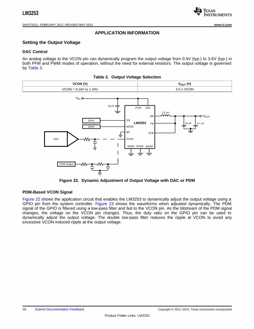
Setting the Output Voltage
DAC Control
An analog voltage to the VCON pin can dynamically program the output voltage from 0.4V (typ.) to 3.6V (typ.) inboth PFM and PWM modes of operation, without the need for external resistors. The output voltage is governedby Table 2.
Table 2. Output Voltage Selection
VCON (V) VOUT (V)
VCON = 0.16V to 1.44V 2.5 x VCON
Figure 22. Dynamic Adjustment of Output Voltage with DAC or PDM
PDM-Based VCON Signal
Figure 22 shows the application circuit that enables the LM3253 to dynamically adjust the output voltage using aGPIO pin from the system controller. Figure 23 shows the waveforms when adjusted dynamically. The PDMsignal of the GPIO is filtered using a low-pass filter and fed to the VCON pin. As the bitstream of the PDM signalchanges, the voltage on the VCON pin changes. Thus, the duty ratio on the GPIO pin can be used todynamically adjust the output voltage. The double low-pass filter reduces the ripple at VCON to avoid anyexcessive VCON-induced ripple at the output voltage.
16 Submit Documentation Feedback Copyright © 2012–2013, Texas Instruments Incorporated
Product Folder Links: LM3253
R1 = 100 k:
C1 = 1.7 pF C2 = 9 pF
8 30 Ps
3.4V 3.4V 3.4V
EN
VCON
VOUT
ILOAD
0V
0A
< 200 mA
8 30 Ps
7 20 Ps
7 20 Ps
7 20 Ps
1V
1.7A7 20 Ps
VCON = 0.4V
LM3253
www.ti.com SNVS791Q –FEBRUARY 2012–REVISED MAY 2013
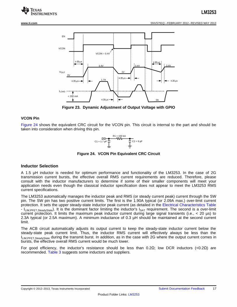
Figure 23. Dynamic Adjustment of Output Voltage with GPIO
VCON Pin
Figure 24 shows the equivalent CRC circuit for the VCON pin. This circuit is internal to the part and should betaken into consideration when driving this pin.
Figure 24. VCON Pin Equivalent CRC Circuit
Inductor Selection
A 1.5 µH inductor is needed for optimum performance and functionality of the LM3253. In the case of 2Gtransmission current bursts, the effective overall RMS current requirements are reduced. Therefore, pleaseconsult with the inductor manufacturers to determine if some of their smaller components will meet yourapplication needs even though the classical inductor specification does not appear to meet the LM3253 RMScurrent specifications.
The LM3253 automatically manages the inductor peak and RMS (or steady current peak) current through the SWpin. The SW pin has two positive current limits. The first is the 1.90A typical (or 2.09A max.) over-limit currentprotection. It sets the upper steady-state inductor peak current (as detailed in the Electrical Characteristics Table- ILIM,PFET,SteadyState). It is the dominant factor limiting the inductor's ISAT requirement. The second is a over-limitcurrent protection. It limits the maximum peak inductor current during large signal transients (i.e., < 20 µs) to2.3A typical (or 2.5A maximum). A minimum inductance of 0.3 µH should be maintained at the second currentlimit.
The ACB circuit automatically adjusts its output current to keep the steady-state inductor current below thesteady-state peak current limit. Thus, the inductor RMS current will effectively always be less than theILIM,PFET,SteadyState during the transmit burst. In addition, as in the case with 2G where the output current comes inbursts, the effective overall RMS current would be much lower.
For good efficiency, the inductor’s resistance should be less than 0.2Ω; low DCR inductors (<0.2Ω) arerecommended. Table 3 suggests some inductors and suppliers.
Copyright © 2012–2013, Texas Instruments Incorporated Submit Documentation Feedback 17
Product Folder Links: LM3253
LM3253
SNVS791Q –FEBRUARY 2012–REVISED MAY 2013 www.ti.com
Table 3. Suggested Inductors and Their Suppliers
Model Vendor Size ISAT - 30% DCR
DFE252010C (1269AS-H-1R5N) TOKO 2.5 mm x 2.0 mm x 1.0 mm 2.7A 90 mΩTFM252010A-1R5M TDK 2.5 mm x 2.0 mm x 1.0 mm 2.9A 80 mΩTFM201610-1R5M TDK 2.0 mm x 1.6 mm x 1.0 mm 2.2A 140 mΩ
Capacitor Selection
The LM3253 is designed to use ceramic capacitors for its input and output filters. Use a 10 µF capacitor for theinput and approximately 10 µF actual total output capacitance. Capacitor types such as X5R, X7R arerecommended for both filters. These provide an optimal balance between small size, cost, reliability andperformance for cell phones and similar applications. Table 4 lists suggested part numbers and suppliers. DCbias characteristics of the capacitors must be considered while selecting the voltage rating and case size of thecapacitor. Smaller case sizes for the output capacitor mitigate piezo-electric vibrations of the capacitor when theoutput voltage is stepped up and down at fast rates. However, they have a bigger percentage drop in value withDC bias. For even smaller total solution size, 0402 case size capacitors are recommended for filtering. Use ofmultiple 2.2 µF or 1 µF capacitors can also be considered. For RF Power Amplifier applications, split the outputcapacitor between DC-DC converter and RF Power Amplifiers: 10 µF (COUT1) + 4.7 µF (COUT2) + 3 x 1 µF (COUT3)is recommended. The optimum capacitance split is application dependent, and for stability the actual totalcapacitance (taking into account effects of capacitor DC bias, temperature de-rating, aging and other capacitortolerances) should target 10 µF with 2.5V DC bias (measured at 0.5 VRMS). Place all the output capacitors veryclose to the respective device. A high-frequency capacitor (3300 pF) is highly recommended to be placed next toCOUT1.
Table 4. Suggested Capacitors and Their Suppliers
Capacitance Model Size (Wx L) (mm) Vendor
10 µF GRM185R60J106M 1.6 x 0.8 Murata
10 µF CL05A106MQ5NUN 1.0 x 0.5 Samsung
4.7 µF CL05A475MQ5NRN 1.0 x 0.5 Samsung
1.0 µF CL03A105MQ3CSN 0.6 x 0.3 Samsung
3300 pF GRM022R60J332K 0.4 x 0.2 Murata
EN Input Control
Use the system controller to drive the EN HIGH or LOW with a comparator, Schmitt trigger or logic gate. Set EN= HIGH (>1.2V) for normal operation and LOW (<0.5V) for shutdown mode to reduce current consumption to0.02 µA (typ.) current.
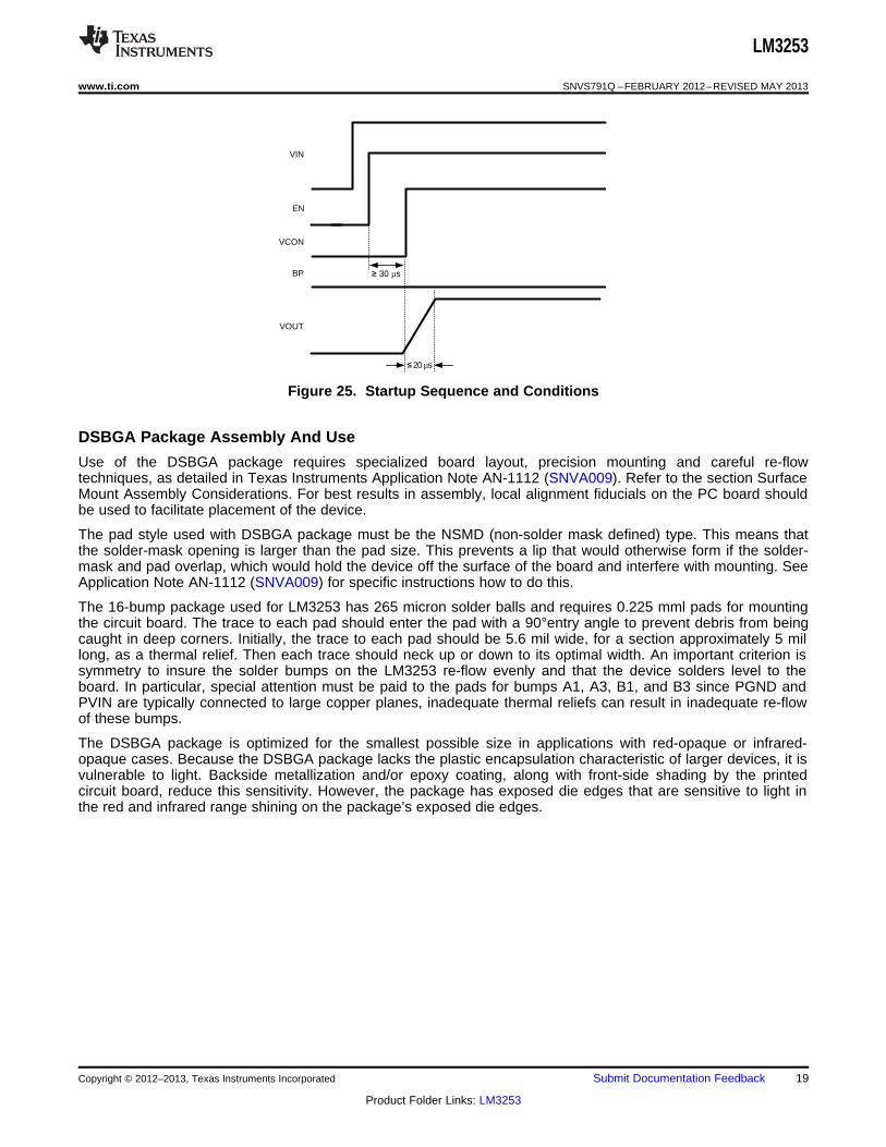
Startup
The waveform Figure 25 in shows the startup condition. First, VIN should take on a value between 2.7V and 5.5V.Next, EN should go HIGH (>1.2V). Finally, VCON should be set to a value that corresponds to the requiredoutput voltage (VOUT = VCON x 2.5). VOUT will reach its steady-state value in less than 50 µs. To optimize thestartup time and behavior of the output voltage, the LM3253 will always start up in PWM mode (even whenMODE = HIGH and output load current ≤ 75mA), then seamlessly transition into PFM mode.
18 Submit Documentation Feedback Copyright © 2012–2013, Texas Instruments Incorporated
Product Folder Links: LM3253
EN
BP
VOUT
7 20 µs
VIN
8 30 µs
VCON
LM3253
www.ti.com SNVS791Q –FEBRUARY 2012–REVISED MAY 2013
Figure 25. Startup Sequence and Conditions
DSBGA Package Assembly And Use
Use of the DSBGA package requires specialized board layout, precision mounting and careful re-flowtechniques, as detailed in Texas Instruments Application Note AN-1112 (SNVA009). Refer to the section SurfaceMount Assembly Considerations. For best results in assembly, local alignment fiducials on the PC board shouldbe used to facilitate placement of the device.
The pad style used with DSBGA package must be the NSMD (non-solder mask defined) type. This means thatthe solder-mask opening is larger than the pad size. This prevents a lip that would otherwise form if the solder-mask and pad overlap, which would hold the device off the surface of the board and interfere with mounting. SeeApplication Note AN-1112 (SNVA009) for specific instructions how to do this.
The 16-bump package used for LM3253 has 265 micron solder balls and requires 0.225 mml pads for mountingthe circuit board. The trace to each pad should enter the pad with a 90°entry angle to prevent debris from beingcaught in deep corners. Initially, the trace to each pad should be 5.6 mil wide, for a section approximately 5 millong, as a thermal relief. Then each trace should neck up or down to its optimal width. An important criterion issymmetry to insure the solder bumps on the LM3253 re-flow evenly and that the device solders level to theboard. In particular, special attention must be paid to the pads for bumps A1, A3, B1, and B3 since PGND andPVIN are typically connected to large copper planes, inadequate thermal reliefs can result in inadequate re-flowof these bumps.
The DSBGA package is optimized for the smallest possible size in applications with red-opaque or infrared-opaque cases. Because the DSBGA package lacks the plastic encapsulation characteristic of larger devices, it isvulnerable to light. Backside metallization and/or epoxy coating, along with front-side shading by the printedcircuit board, reduce this sensitivity. However, the package has exposed die edges that are sensitive to light inthe red and infrared range shining on the package’s exposed die edges.
Copyright © 2012–2013, Texas Instruments Incorporated Submit Documentation Feedback 19
Product Folder Links: LM3253

LM3253
SNVS791Q –FEBRUARY 2012–REVISED MAY 2013 www.ti.com
Board Layout Considerations
PC board layout is an important part of DC-DC converter design. Please contact TI for detailed PCB layoutguidelines. Poor board layout can disrupt the performance of a DC-DC converter and surrounding circuitry bycontributing to EMI, ground bounce, and resistive voltage loss in the traces. These can send erroneous signals tothe DC-DC converter IC, resulting in poor regulation or instability. Poor layout can also result in re-flow problemsleading to poor solder joints between the DSBGA package and the board pads, which can result in erratic ordegraded performance. Good layout for the LM3253 can be implemented by following a few simple design rules.1. Place the LM3253 on pads with a pad size of 0.225 mm and a solder mask opening of 0.325 mm. As a
thermal relief, connect to each pad to a trace that has maximally the same width as the solder mask openingand incrementally increase each trace to its optimal width. Each board trace connecting to the solder maskopening should be exactly the same width. This important criterion of symmetry is to insure that the solderbumps on the LM3253 re-flow evenly (see AN-1112: Surface Mount Assembly Considerations) (SNVA009).
2. Place the LM3253, inductor and filter capacitors close together and make the trace short. The tracesbetween these components carry relatively high switching currents and act as antennas. Following this rulereduces radiated noise. Place the capacitors and inductor within 0.3 mm of the LM3253.
3. Arrange the components so that the switching current loops curl in the same direction. During the first half ofeach cycle, current flows from the input filter capacitor through the LM3253 and inductor to the output filtercapacitor and back through ground, forming a current loop. In the second half of each cycle, current is pulledup from ground through the LM3253 by the inductor, to the output filter capacitor and then back throughground, forming a second current loop. Routing these loops so the current curls in the same directionprevents magnetic field reversal between the two half-cycles and reduces radiated noise.
4. Connect the ground pins of the LM3253 and filter capacitors together at a single-star connection usinggenerous component-side copper fill as a pseudo-ground plane. Then connect this to the ground-plane (ifone is used) with multiple vias in parallel. This reduces ground-plane noise by preventing the switchingcurrents from circulating through the ground plane. It also reduces ground bounce at the LM3253 by giving ita low-impedance ground connection.
5. Use wide traces between the power components and for power connections to the DC-DC converter circuit.This reduces voltage errors caused by resistive losses across the traces.
6. Route noise sensitive traces, such as the voltage feedback path, away from noisy traces between the powercomponents (such as SW trace to the inductor). The voltage feedback trace must remain close to theLM3253 circuit and should be routed directly from FB to VOUT at the output capacitor and should be routedopposite to noise components. This reduces EMI radiated onto the DC-DC converter’s own voltage feedbacktrace.
7. Split up output capacitors between LM3253 output and PA(s). Suggestion is to place one-half of outputcapacitance as close as possible to LM3253 output and the rest as close as possible to PA(s).
20 Submit Documentation Feedback Copyright © 2012–2013, Texas Instruments Incorporated
Product Folder Links: LM3253
PACKAGE OPTION ADDENDUM
www.ti.com 10-Dec-2020
Addendum-Page 1
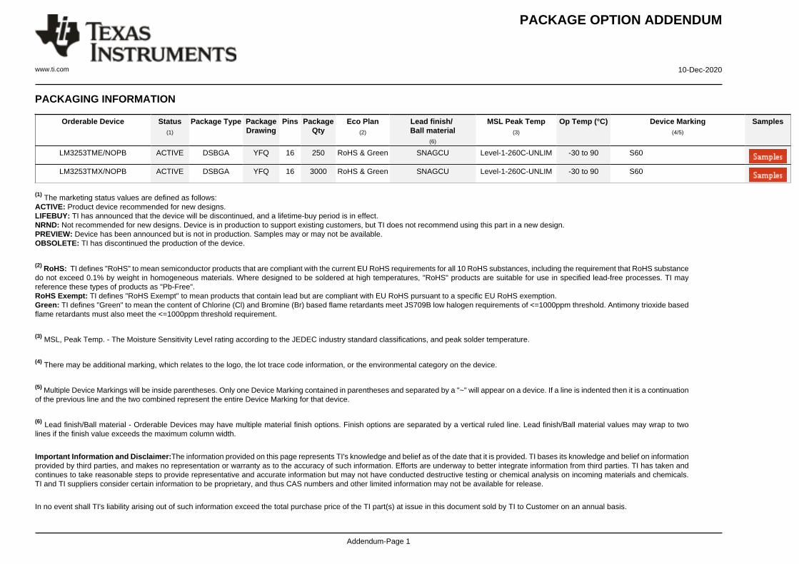
PACKAGING INFORMATION
Orderable Device Status(1)
Package Type PackageDrawing
Pins PackageQty
Eco Plan(2)
Lead finish/Ball material
(6)
MSL Peak Temp(3)
Op Temp (°C) Device Marking(4/5)
Samples
LM3253TME/NOPB ACTIVE DSBGA YFQ 16 250 RoHS & Green SNAGCU Level-1-260C-UNLIM -30 to 90 S60
LM3253TMX/NOPB ACTIVE DSBGA YFQ 16 3000 RoHS & Green SNAGCU Level-1-260C-UNLIM -30 to 90 S60
(1) The marketing status values are defined as follows:ACTIVE: Product device recommended for new designs.LIFEBUY: TI has announced that the device will be discontinued, and a lifetime-buy period is in effect.NRND: Not recommended for new designs. Device is in production to support existing customers, but TI does not recommend using this part in a new design.PREVIEW: Device has been announced but is not in production. Samples may or may not be available.OBSOLETE: TI has discontinued the production of the device.
(2) RoHS: TI defines "RoHS" to mean semiconductor products that are compliant with the current EU RoHS requirements for all 10 RoHS substances, including the requirement that RoHS substancedo not exceed 0.1% by weight in homogeneous materials. Where designed to be soldered at high temperatures, "RoHS" products are suitable for use in specified lead-free processes. TI mayreference these types of products as "Pb-Free".RoHS Exempt: TI defines "RoHS Exempt" to mean products that contain lead but are compliant with EU RoHS pursuant to a specific EU RoHS exemption.Green: TI defines "Green" to mean the content of Chlorine (Cl) and Bromine (Br) based flame retardants meet JS709B low halogen requirements of <=1000ppm threshold. Antimony trioxide basedflame retardants must also meet the <=1000ppm threshold requirement.
(3) MSL, Peak Temp. - The Moisture Sensitivity Level rating according to the JEDEC industry standard classifications, and peak solder temperature.
(4) There may be additional marking, which relates to the logo, the lot trace code information, or the environmental category on the device.
(5) Multiple Device Markings will be inside parentheses. Only one Device Marking contained in parentheses and separated by a "~" will appear on a device. If a line is indented then it is a continuationof the previous line and the two combined represent the entire Device Marking for that device.
(6) Lead finish/Ball material - Orderable Devices may have multiple material finish options. Finish options are separated by a vertical ruled line. Lead finish/Ball material values may wrap to twolines if the finish value exceeds the maximum column width.
Important Information and Disclaimer:The information provided on this page represents TI's knowledge and belief as of the date that it is provided. TI bases its knowledge and belief on informationprovided by third parties, and makes no representation or warranty as to the accuracy of such information. Efforts are underway to better integrate information from third parties. TI has taken andcontinues to take reasonable steps to provide representative and accurate information but may not have conducted destructive testing or chemical analysis on incoming materials and chemicals.TI and TI suppliers consider certain information to be proprietary, and thus CAS numbers and other limited information may not be available for release.
In no event shall TI's liability arising out of such information exceed the total purchase price of the TI part(s) at issue in this document sold by TI to Customer on an annual basis.

PACKAGE OPTION ADDENDUM
www.ti.com 10-Dec-2020
Addendum-Page 2

TAPE AND REEL INFORMATION
*All dimensions are nominal
Device PackageType
PackageDrawing
Pins SPQ ReelDiameter
(mm)
ReelWidth
W1 (mm)
A0(mm)
B0(mm)
K0(mm)
P1(mm)
W(mm)
Pin1Quadrant
LM3253TME/NOPB DSBGA YFQ 16 250 178.0 8.4 2.08 2.08 0.76 4.0 8.0 Q1
LM3253TMX/NOPB DSBGA YFQ 16 3000 178.0 8.4 2.08 2.08 0.76 4.0 8.0 Q1
PACKAGE MATERIALS INFORMATION
www.ti.com 25-Jun-2013
Pack Materials-Page 1

*All dimensions are nominal
Device Package Type Package Drawing Pins SPQ Length (mm) Width (mm) Height (mm)
LM3253TME/NOPB DSBGA YFQ 16 250 210.0 185.0 35.0
LM3253TMX/NOPB DSBGA YFQ 16 3000 210.0 185.0 35.0
PACKAGE MATERIALS INFORMATION
www.ti.com 25-Jun-2013
Pack Materials-Page 2
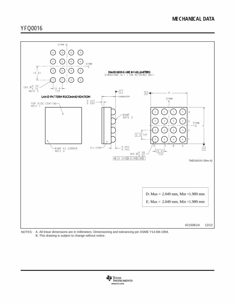
MECHANICAL DATA
YFQ0016xxx
www.ti.com
TMD16XXX (Rev A)
E
0.600±0.075
D
A. All linear dimensions are in millimeters. Dimensioning and tolerancing per ASME Y14.5M-1994.B. This drawing is subject to change without notice.
NOTES:
4215081/A 12/12
D: Max =
E: Max =
2.049 mm, Min =
2.049 mm, Min =
1.989 mm
1.989 mm

IMPORTANT NOTICE AND DISCLAIMER
TI PROVIDES TECHNICAL AND RELIABILITY DATA (INCLUDING DATASHEETS), DESIGN RESOURCES (INCLUDING REFERENCE DESIGNS), APPLICATION OR OTHER DESIGN ADVICE, WEB TOOLS, SAFETY INFORMATION, AND OTHER RESOURCES “AS IS” AND WITH ALL FAULTS, AND DISCLAIMS ALL WARRANTIES, EXPRESS AND IMPLIED, INCLUDING WITHOUT LIMITATION ANY IMPLIED WARRANTIES OF MERCHANTABILITY, FITNESS FOR A PARTICULAR PURPOSE OR NON-INFRINGEMENT OF THIRD PARTY INTELLECTUAL PROPERTY RIGHTS.These resources are intended for skilled developers designing with TI products. You are solely responsible for (1) selecting the appropriate TI products for your application, (2) designing, validating and testing your application, and (3) ensuring your application meets applicable standards, and any other safety, security, or other requirements. These resources are subject to change without notice. TI grants you permission to use these resources only for development of an application that uses the TI products described in the resource. Other reproduction and display of these resources is prohibited. No license is granted to any other TI intellectual property right or to any third party intellectual property right. TI disclaims responsibility for, and you will fully indemnify TI and its representatives against, any claims, damages, costs, losses, and liabilities arising out of your use of these resources.TI’s products are provided subject to TI’s Terms of Sale (www.ti.com/legal/termsofsale.html) or other applicable terms available either on ti.com or provided in conjunction with such TI products. TI’s provision of these resources does not expand or otherwise alter TI’s applicable warranties or warranty disclaimers for TI products.
Mailing Address: Texas Instruments, Post Office Box 655303, Dallas, Texas 75265Copyright © 2020, Texas Instruments Incorporated