Embed Size (px)
Citation preview
SN74HC7001 Quadruple 2-Input AND Gates with Schmitt-Trigger Inputs
1 Features• Buffered inputs• Wide operating voltage range: 2 V to 6 V• Wide operating temperature range:
–40°C to +85°C• Supports fanout up to 10 LSTTL loads• Significant power reduction compared to LSTTL
logic ICs
2 Applications• Combining power good signals• Enable digital signals
3 DescriptionThis device contains four independent 2-input ANDgates with Schmitt-trigger inputs. Each gate performsthe Boolean function Y = A B in positive logic.
Device Information(1)
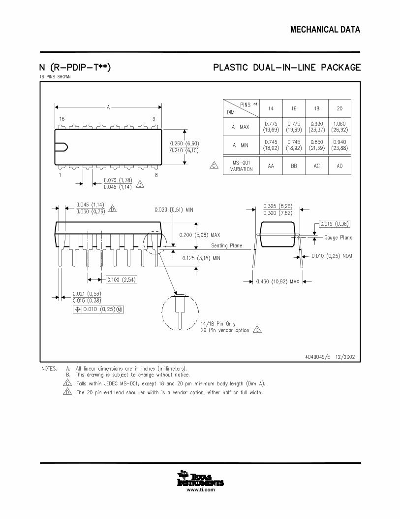
PART NUMBER PACKAGE BODY SIZE (NOM)SN74HC7001D SOIC (14) 8.70 mm × 3.90 mm
SN74HC7001N PDIP (14) 19.30 mm × 6.40 mm
(1) For all available packages, see the orderable addendum atthe end of the data sheet.
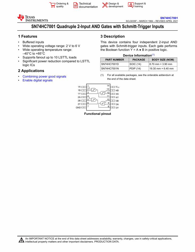
1
2
3
7
4
5
6
14
13
12
8
11
10
9
1A
1B
1Y
2A
2B
2Y
GND
4B
4A
4Y
3B
3A
VCC
3Y
Functional pinout
www.ti.comSN74HC7001
SCLS035F – MARCH 1984 – REVISED APRIL 2021
Copyright © 2021 Texas Instruments Incorporated Submit Document Feedback 1
Product Folder Links: SN74HC7001
SN74HC7001SCLS035F – MARCH 1984 – REVISED APRIL 2021
An IMPORTANT NOTICE at the end of this data sheet addresses availability, warranty, changes, use in safety-critical applications,intellectual property matters and other important disclaimers. PRODUCTION DATA.
Table of Contents1 Features............................................................................12 Applications..................................................................... 13 Description.......................................................................14 Revision History.............................................................. 25 Pin Configuration and Functions...................................3
Pin Functions.................................................................... 36 Specifications.................................................................. 4
6.1 Absolute Maximum Ratings........................................ 46.2 Recommended Operating Conditions.........................46.3 Thermal Information....................................................46.4 Electrical Characteristics.............................................56.5 Switching Characteristics............................................56.6 Operating Characteristics........................................... 56.7 Typical Characteristics................................................ 6
7 Parameter Measurement Information............................ 78 Detailed Description........................................................8
8.1 Overview..................................................................... 88.2 Functional Block Diagram........................................... 8
8.3 Feature Description.....................................................88.4 Device Functional Modes............................................9
9 Application and Implementation.................................. 109.1 Application Information............................................. 109.2 Typical Application.................................................... 10
10 Power Supply Recommendations..............................1211 Layout...........................................................................12
11.1 Layout Guidelines................................................... 1211.2 Layout Example...................................................... 12
12 Device and Documentation Support..........................1312.1 Documentation Support.......................................... 1312.2 Related Links.......................................................... 1312.3 Support Resources................................................. 1312.4 Trademarks.............................................................1312.5 Electrostatic Discharge Caution..............................1312.6 Glossary..................................................................13
13 Mechanical, Packaging, and OrderableInformation.................................................................... 13
4 Revision HistoryNOTE: Page numbers for previous revisions may differ from page numbers in the current version.
Changes from Revision E (November 2004) to Revision F (April 2021) Page• Updated the numbering format for tables, figures, and cross-references throughout the document..................1• Updated to new data sheet standards................................................................................................................ 1• RθJA increased for the D (86 to 133.6 /W) and NS (76 to 122.6 /W) packages and decreased for the N
package (80 to 61.4 /W)..................................................................................................................................4
SN74HC7001SCLS035F – MARCH 1984 – REVISED APRIL 2021 www.ti.com
2 Submit Document Feedback Copyright © 2021 Texas Instruments Incorporated
Product Folder Links: SN74HC7001
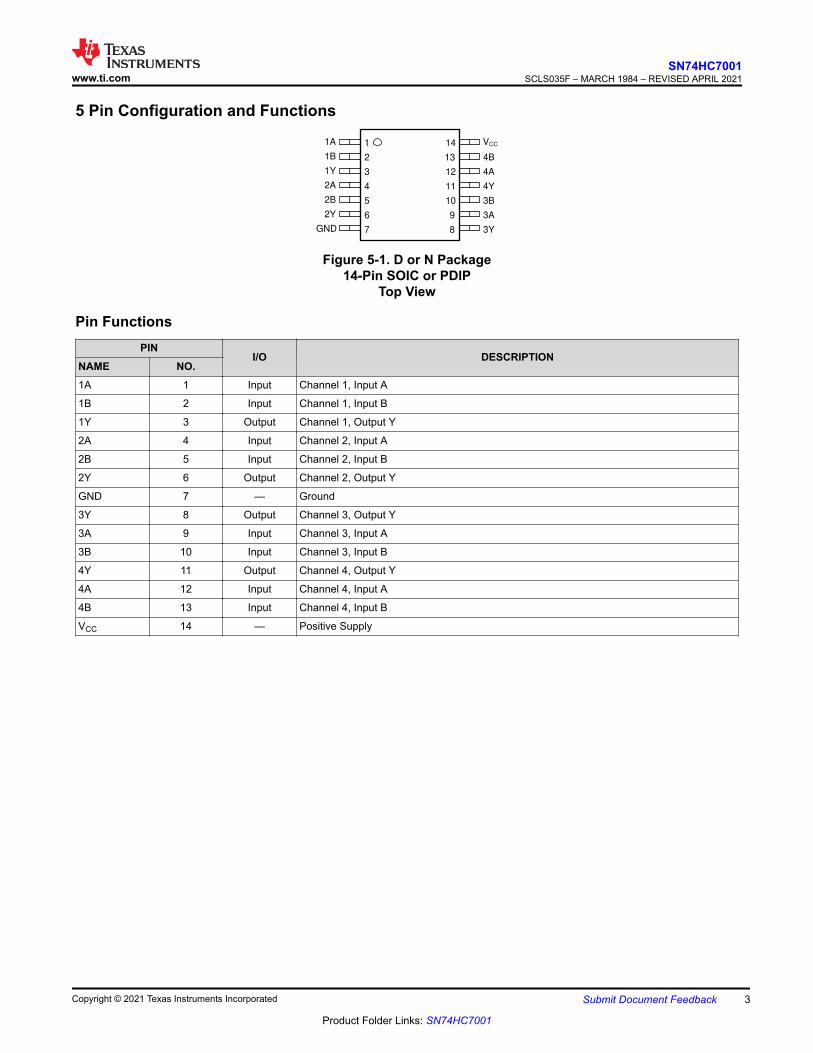
5 Pin Configuration and Functions
1
2
3
7
4
5
6
14
13
12
8
11
10
9
1A
1B
1Y
2A
2B
2Y
GND
4B
4A
4Y
3B
3A
VCC
3Y
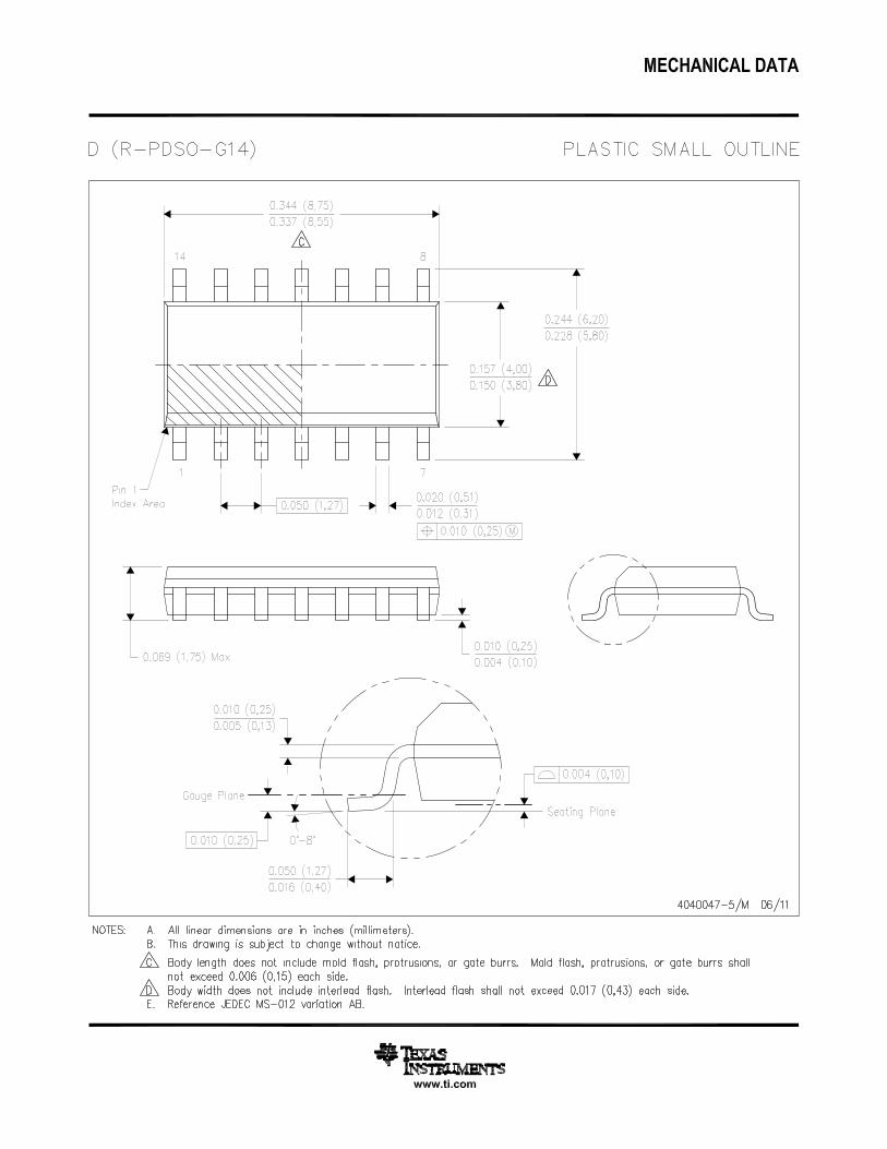
Figure 5-1. D or N Package14-Pin SOIC or PDIP
Top View
Pin FunctionsPIN
I/O DESCRIPTIONNAME NO.1A 1 Input Channel 1, Input A
1B 2 Input Channel 1, Input B
1Y 3 Output Channel 1, Output Y
2A 4 Input Channel 2, Input A
2B 5 Input Channel 2, Input B
2Y 6 Output Channel 2, Output Y
GND 7 — Ground
3Y 8 Output Channel 3, Output Y
3A 9 Input Channel 3, Input A
3B 10 Input Channel 3, Input B
4Y 11 Output Channel 4, Output Y
4A 12 Input Channel 4, Input A
4B 13 Input Channel 4, Input B
VCC 14 — Positive Supply
www.ti.comSN74HC7001
SCLS035F – MARCH 1984 – REVISED APRIL 2021
Copyright © 2021 Texas Instruments Incorporated Submit Document Feedback 3
Product Folder Links: SN74HC7001
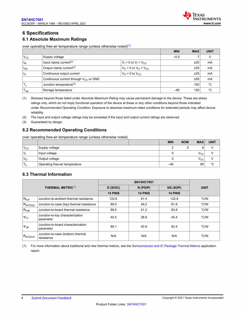
6 Specifications6.1 Absolute Maximum Ratingsover operating free-air temperature range (unless otherwise noted)(1)
MIN MAX UNITVCC Supply voltage –0.5 7 V
IIK Input clamp current(2) VI < 0 or VI > VCC ±20 mA
IOK Output clamp current(2) VO < 0 or VO > VCC ±20 mA
IO Continuous output current VO = 0 to VCC ±25 mA
Continuous current through VCC or GND ±50 mA
TJ Junction temperature(3) 150 °C
Tstg Storage temperature –65 150 °C
(1) Stresses beyond those listed under Absolute Maximum Rating may cause permanent damage to the device. These are stressratings only, which do not imply functional operation of the device at these or any other conditions beyond those indicatedunder Recommended Operating Condition. Exposure to absolute-maximum-rated conditions for extended periods may affect devicereliability.
(2) The input and output voltage ratings may be exceeded if the input and output current ratings are observed.(3) Guaranteed by design.
6.2 Recommended Operating Conditionsover operating free-air temperature range (unless otherwise noted)
MIN NOM MAX UNITVCC Supply voltage 2 5 6 V
VI Input voltage 0 VCC V
VO Output voltage 0 VCC V
TA Operating free-air temperature –40 85 °C
6.3 Thermal Information
THERMAL METRIC(1)
SN74HC7001UNITD (SOIC) N (PDIP) NS (SOP)
14 PINS 14 PINS 14 PINSRθJA Junction-to-ambient thermal resistance 133.6 61.4 122.6 °C/W
RθJC(top) Junction-to-case (top) thermal resistance 89.0 49.2 81.8 °C/W
RθJB Junction-to-board thermal resistance 89.5 41.2 83.8 °C/W
ΨJTJunction-to-top characterizationparameter 45.5 28.8 45.4 °C/W
ΨJBJunction-to-board characterizationparameter 89.1 40.9 83.4 °C/W
RθJC(bot)Junction-to-case (bottom) thermalresistance N/A N/A N/A °C/W
(1) For more information about traditional and new thermal metrics, see the Semiconductor and IC Package Thermal Metrics applicationreport.
SN74HC7001SCLS035F – MARCH 1984 – REVISED APRIL 2021 www.ti.com
4 Submit Document Feedback Copyright © 2021 Texas Instruments Incorporated
Product Folder Links: SN74HC7001
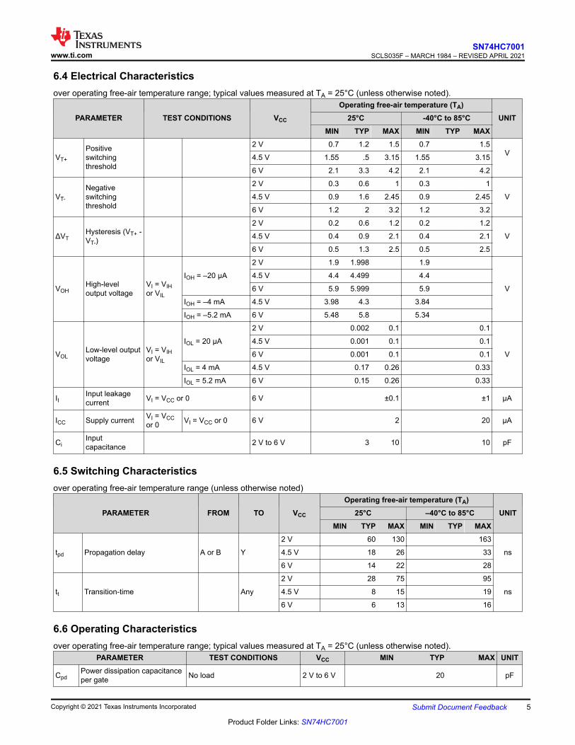
6.4 Electrical Characteristicsover operating free-air temperature range; typical values measured at TA = 25°C (unless otherwise noted).
PARAMETER TEST CONDITIONS VCC
Operating free-air temperature (TA)UNIT25°C -40°C to 85°C
MIN TYP MAX MIN TYP MAX
VT+
Positiveswitchingthreshold
2 V 0.7 1.2 1.5 0.7 1.5V 4.5 V 1.55 .5 3.15 1.55 3.15
6 V 2.1 3.3 4.2 2.1 4.2
VT-
Negativeswitchingthreshold
2 V 0.3 0.6 1 0.3 1
V4.5 V 0.9 1.6 2.45 0.9 2.45
6 V 1.2 2 3.2 1.2 3.2
ΔVTHysteresis (VT+ -VT-)
2 V 0.2 0.6 1.2 0.2 1.2
V4.5 V 0.4 0.9 2.1 0.4 2.1
6 V 0.5 1.3 2.5 0.5 2.5
VOHHigh-leveloutput voltage
VI = VIHor VIL
IOH = –20 µA
2 V 1.9 1.998 1.9
V
4.5 V 4.4 4.499 4.4
6 V 5.9 5.999 5.9
IOH = –4 mA 4.5 V 3.98 4.3 3.84
IOH = –5.2 mA 6 V 5.48 5.8 5.34
VOLLow-level outputvoltage
VI = VIHor VIL
IOL = 20 µA
2 V 0.002 0.1 0.1
V
4.5 V 0.001 0.1 0.1
6 V 0.001 0.1 0.1
IOL = 4 mA 4.5 V 0.17 0.26 0.33
IOL = 5.2 mA 6 V 0.15 0.26 0.33
IIInput leakagecurrent VI = VCC or 0 6 V ±0.1 ±1 µA
ICC Supply current VI = VCCor 0 VI = VCC or 0 6 V 2 20 µA
CiInputcapacitance 2 V to 6 V 3 10 10 pF
6.5 Switching Characteristicsover operating free-air temperature range (unless otherwise noted)
PARAMETER FROM TO VCC
Operating free-air temperature (TA)UNIT25°C –40°C to 85°C
MIN TYP MAX MIN TYP MAX
tpd Propagation delay A or B Y
2 V 60 130 163
ns4.5 V 18 26 33
6 V 14 22 28
tt Transition-time Any
2 V 28 75 95
ns4.5 V 8 15 19
6 V 6 13 16
6.6 Operating Characteristicsover operating free-air temperature range; typical values measured at TA = 25°C (unless otherwise noted).
PARAMETER TEST CONDITIONS VCC MIN TYP MAX UNIT
CpdPower dissipation capacitanceper gate No load 2 V to 6 V 20 pF
www.ti.comSN74HC7001
SCLS035F – MARCH 1984 – REVISED APRIL 2021
Copyright © 2021 Texas Instruments Incorporated Submit Document Feedback 5
Product Folder Links: SN74HC7001
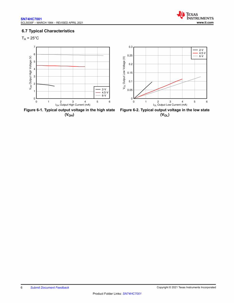
6.7 Typical CharacteristicsTA = 25°C
IOH Output High Current (mA)
VO
H O
utp
ut H
igh V
oltag
e (
V)
0 1 2 3 4 5 60
1
2
3
4
5
6
7
2-V4.5-V6-V
Figure 6-1. Typical output voltage in the high state(VOH)
IOL Output Low Current (mA)
VO
L O
utp
ut L
ow
Vo
ltag
e (
V)
0 1 2 3 4 5 60
0.05
0.1
0.15
0.2
0.25
0.32-V4.5-V6-V
Figure 6-2. Typical output voltage in the low state(VOL)
SN74HC7001SCLS035F – MARCH 1984 – REVISED APRIL 2021 www.ti.com
6 Submit Document Feedback Copyright © 2021 Texas Instruments Incorporated
Product Folder Links: SN74HC7001
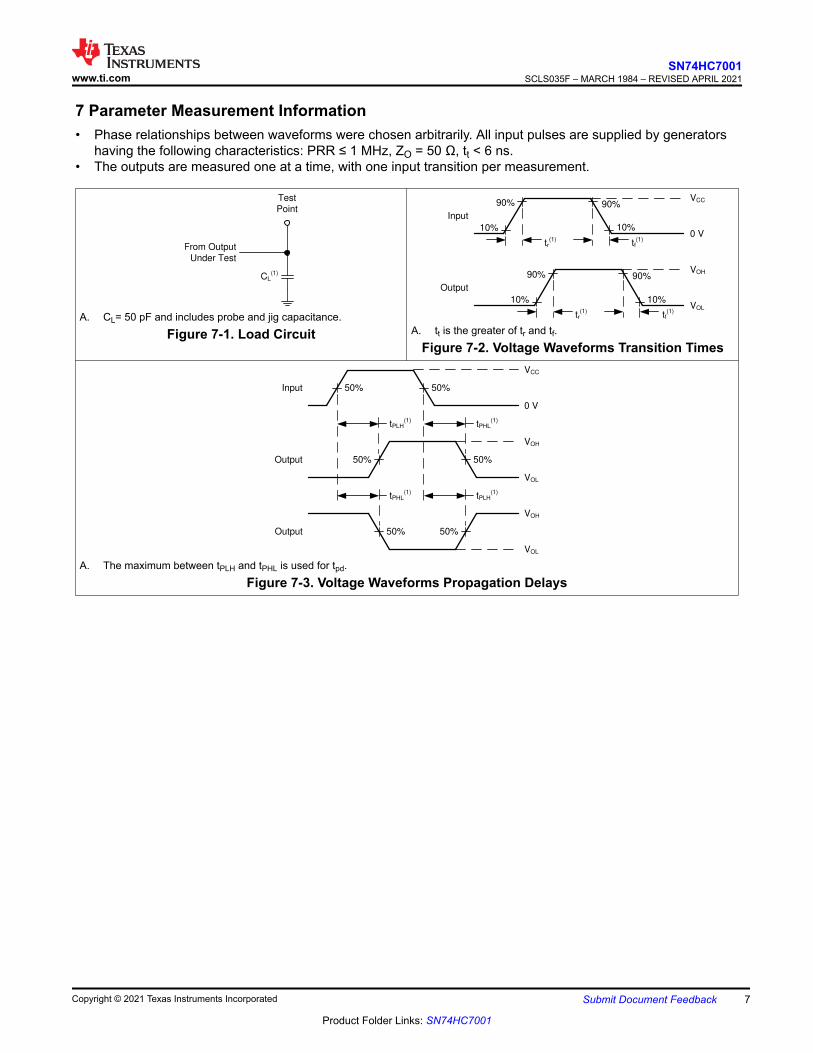
7 Parameter Measurement Information• Phase relationships between waveforms were chosen arbitrarily. All input pulses are supplied by generators
having the following characteristics: PRR ≤ 1 MHz, ZO = 50 Ω, tt < 6 ns.• The outputs are measured one at a time, with one input transition per measurement.
CL(1)
From Output
Under Test
Test
Point
A. CL= 50 pF and includes probe and jig capacitance.Figure 7-1. Load Circuit
VOH
VOL
Output
VCC
0 V
Input
tf(1)tr
(1)
90%
10%
90%
10%
tr(1)
90%
10%
tf(1)
90%
10%
A. tt is the greater of tr and tf.Figure 7-2. Voltage Waveforms Transition Times
50%Input 50%
VCC
0 V
50% 50%
VOH
VOL
tPLH(1) tPHL
(1)
VOH
VOL
tPHL(1) tPLH
(1)
Output
Output 50% 50%
A. The maximum between tPLH and tPHL is used for tpd.Figure 7-3. Voltage Waveforms Propagation Delays
www.ti.comSN74HC7001
SCLS035F – MARCH 1984 – REVISED APRIL 2021
Copyright © 2021 Texas Instruments Incorporated Submit Document Feedback 7
Product Folder Links: SN74HC7001
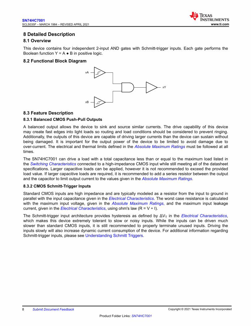
8 Detailed Description8.1 OverviewThis device contains four independent 2-input AND gates with Schmitt-trigger inputs. Each gate performs theBoolean function Y = A B in positive logic.
8.2 Functional Block Diagram
xA
xB
xY
8.3 Feature Description8.3.1 Balanced CMOS Push-Pull Outputs
A balanced output allows the device to sink and source similar currents. The drive capability of this devicemay create fast edges into light loads so routing and load conditions should be considered to prevent ringing.Additionally, the outputs of this device are capable of driving larger currents than the device can sustain withoutbeing damaged. It is important for the output power of the device to be limited to avoid damage due toover-current. The electrical and thermal limits defined in the Absolute Maximum Ratings must be followed at alltimes.
The SN74HC7001 can drive a load with a total capacitance less than or equal to the maximum load listed inthe Switching Characteristics connected to a high-impedance CMOS input while still meeting all of the datasheetspecifications. Larger capacitive loads can be applied, however it is not recommended to exceed the providedload value. If larger capacitive loads are required, it is recommended to add a series resistor between the outputand the capacitor to limit output current to the values given in the Absolute Maximum Ratings.
8.3.2 CMOS Schmitt-Trigger Inputs
Standard CMOS inputs are high impedance and are typically modeled as a resistor from the input to ground inparallel with the input capacitance given in the Electrical Characteristics. The worst case resistance is calculatedwith the maximum input voltage, given in the Absolute Maximum Ratings, and the maximum input leakagecurrent, given in the Electrical Characteristics, using ohm's law (R = V ÷ I).
The Schmitt-trigger input architecture provides hysteresis as defined by ΔVT in the Electrical Characteristics,which makes this device extremely tolerant to slow or noisy inputs. While the inputs can be driven muchslower than standard CMOS inputs, it is still recommended to properly terminate unused inputs. Driving theinputs slowly will also increase dynamic current consumption of the device. For additional information regardingSchmitt-trigger inputs, please see Understanding Schmitt Triggers.
SN74HC7001SCLS035F – MARCH 1984 – REVISED APRIL 2021 www.ti.com
8 Submit Document Feedback Copyright © 2021 Texas Instruments Incorporated
Product Folder Links: SN74HC7001
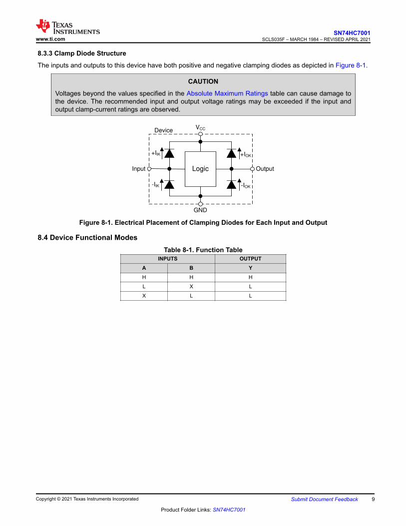
8.3.3 Clamp Diode Structure
The inputs and outputs to this device have both positive and negative clamping diodes as depicted in Figure 8-1.
CAUTION
Voltages beyond the values specified in the Absolute Maximum Ratings table can cause damage tothe device. The recommended input and output voltage ratings may be exceeded if the input andoutput clamp-current ratings are observed.
GND
LogicInput Output
VCCDevice
-IIK
+IIK +IOK
-IOK
Figure 8-1. Electrical Placement of Clamping Diodes for Each Input and Output
8.4 Device Functional ModesTable 8-1. Function Table
INPUTS OUTPUTA B YH H H
L X L
X L L
www.ti.comSN74HC7001
SCLS035F – MARCH 1984 – REVISED APRIL 2021
Copyright © 2021 Texas Instruments Incorporated Submit Document Feedback 9
Product Folder Links: SN74HC7001
9 Application and ImplementationNote
Information in the following applications sections is not part of the TI component specification,and TI does not warrant its accuracy or completeness. TI’s customers are responsible fordetermining suitability of components for their purposes, as well as validating and testing their designimplementation to confirm system functionality.
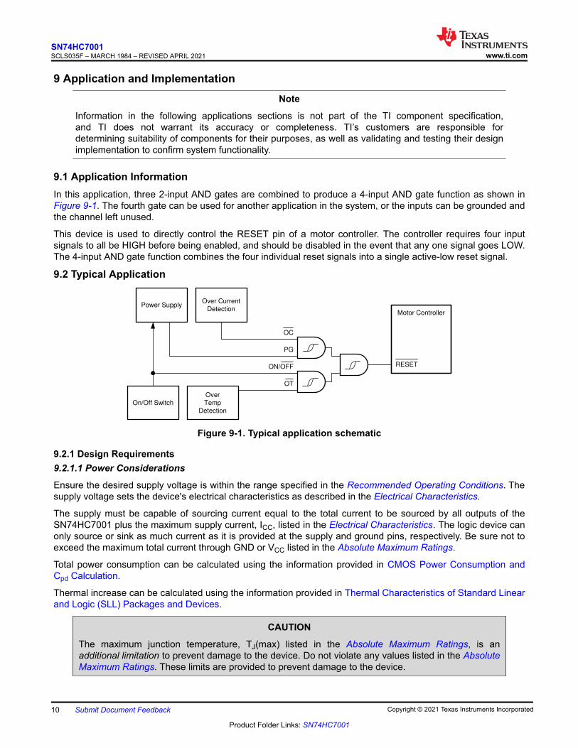
9.1 Application InformationIn this application, three 2-input AND gates are combined to produce a 4-input AND gate function as shown inFigure 9-1. The fourth gate can be used for another application in the system, or the inputs can be grounded andthe channel left unused.
This device is used to directly control the RESET pin of a motor controller. The controller requires four inputsignals to all be HIGH before being enabled, and should be disabled in the event that any one signal goes LOW.The 4-input AND gate function combines the four individual reset signals into a single active-low reset signal.
9.2 Typical Application
OC
PG
ON/OFF RESET
Power SupplyMotor Controller
On/Off Switch
Over
Temp
Detection
Over Current
Detection
OT
Figure 9-1. Typical application schematic
9.2.1 Design Requirements9.2.1.1 Power Considerations
Ensure the desired supply voltage is within the range specified in the Recommended Operating Conditions. Thesupply voltage sets the device's electrical characteristics as described in the Electrical Characteristics.
The supply must be capable of sourcing current equal to the total current to be sourced by all outputs of theSN74HC7001 plus the maximum supply current, ICC, listed in the Electrical Characteristics. The logic device canonly source or sink as much current as it is provided at the supply and ground pins, respectively. Be sure not toexceed the maximum total current through GND or VCC listed in the Absolute Maximum Ratings.
Total power consumption can be calculated using the information provided in CMOS Power Consumption andCpd Calculation.
Thermal increase can be calculated using the information provided in Thermal Characteristics of Standard Linearand Logic (SLL) Packages and Devices.
CAUTION
The maximum junction temperature, TJ(max) listed in the Absolute Maximum Ratings, is anadditional limitation to prevent damage to the device. Do not violate any values listed in the AbsoluteMaximum Ratings. These limits are provided to prevent damage to the device.
SN74HC7001SCLS035F – MARCH 1984 – REVISED APRIL 2021 www.ti.com
10 Submit Document Feedback Copyright © 2021 Texas Instruments Incorporated
Product Folder Links: SN74HC7001
9.2.1.2 Input Considerations
Input signals must cross Vt-(min) to be considered a logic LOW, and Vt+(max) to be considered a logic HIGH. Donot exceed the maximum input voltage range found in the Absolute Maximum Ratings .
Unused inputs must be terminated to either VCC or ground. These can be directly terminated if the input iscompletely unused, or they can be connected with a pull-up or pull-down resistor if the input is to be usedsometimes, but not always. A pull-up resistor is used for a default state of HIGH, and a pull-down resistor isused for a default state of LOW. The resistor size is limited by drive current of the controller, leakage current intothe SN74HC7001, as specified in the Electrical Characteristics , and the desired input transition rate. A 10-kΩresistor value is often used due to these factors.
The SN74HC7001 has no input signal transition rate requirements because it has Schmitt-trigger inputs.
Another benefit to having Schmitt-trigger inputs is the ability to reject noise. Noise with a large enough amplitudecan still cause issues. To know how much noise is too much, please refer to the ΔVT(min) in the ElectricalCharacteristics . This hysteresis value will provide the peak-to-peak limit.
Unlike what happens with standard CMOS inputs, Schmitt-trigger inputs can be held at any valid value withoutcausing huge increases in power consumption. The typical additional current caused by holding an input at avalue other than VCC or ground is plotted in the Typical Characteristics.
Refer to Section 8.3 for additional information regarding the inputs for this device.
9.2.1.3 Output Considerations
The positive supply voltage is used to produce the output HIGH voltage. Drawing current from the output willdecrease the output voltage as specified by the VOH specification in the Electrical Characteristics. Similarly, theground voltage is used to produce the output LOW voltage. Sinking current into the output will increase theoutput voltage as specified by the VOL specification in the Electrical Characteristics.
Unused outputs can be left floating. Do not connect outputs directly to VCC or ground.
Refer to Section 8.3 for additional information regarding the outputs for this device.
9.2.2 Detailed Design Procedure
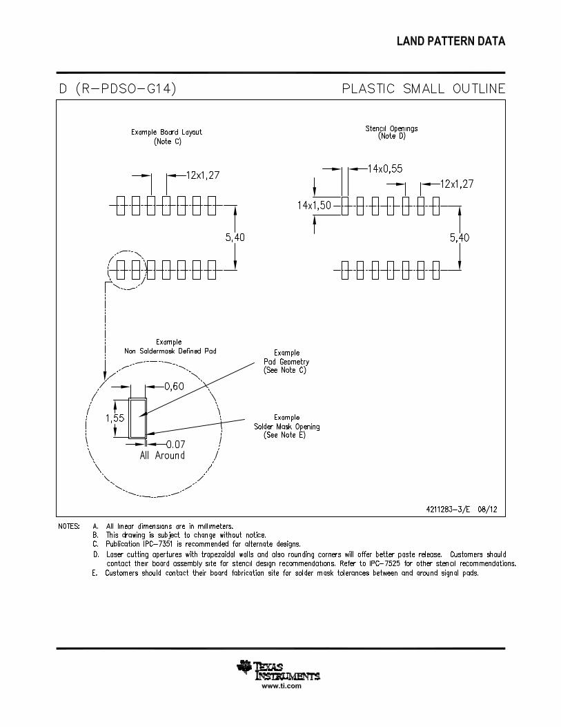
1. Add a decoupling capacitor from VCC to GND. The capacitor needs to be placed physically close to thedevice and electrically close to both the VCC and GND pins. An example layout is shown in the Section 11.
2. Ensure the capacitive load at the output is ≤ 70 pF. This is not a hard limit, however it will ensureoptimal performance. This can be accomplished by providing short, appropriately sized traces from theSN74HC7001 to the receiving device.
3. Ensure the resistive load at the output is larger than (VCC / IO(max)) Ω. This will ensure that the maximumoutput current from the Absolute Maximum Ratings is not violated. Most CMOS inputs have a resistive loadmeasured in megaohms; much larger than the minimum calculated above.
4. Thermal issues are rarely a concern for logic gates, however the power consumption and thermal increasecan be calculated using the steps provided in the application report, CMOS Power Consumption and CpdCalculation
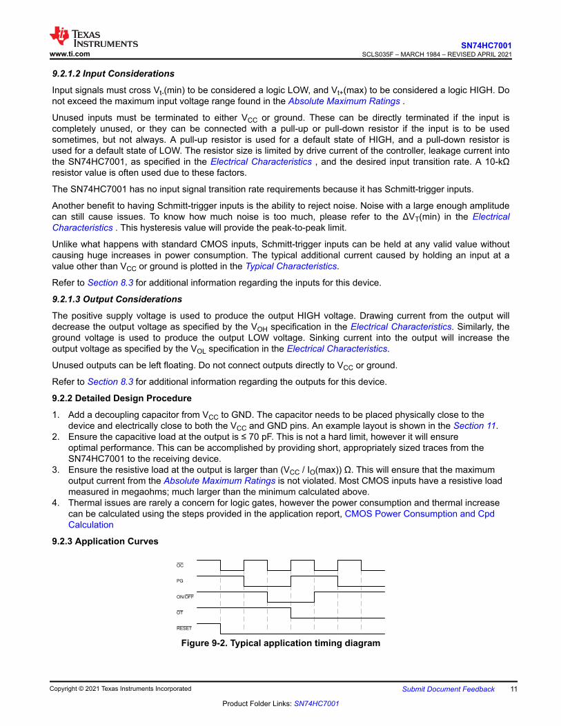
9.2.3 Application Curves
OC
PG
ON/OFF
OT
RESET
Figure 9-2. Typical application timing diagram
www.ti.comSN74HC7001
SCLS035F – MARCH 1984 – REVISED APRIL 2021
Copyright © 2021 Texas Instruments Incorporated Submit Document Feedback 11
Product Folder Links: SN74HC7001
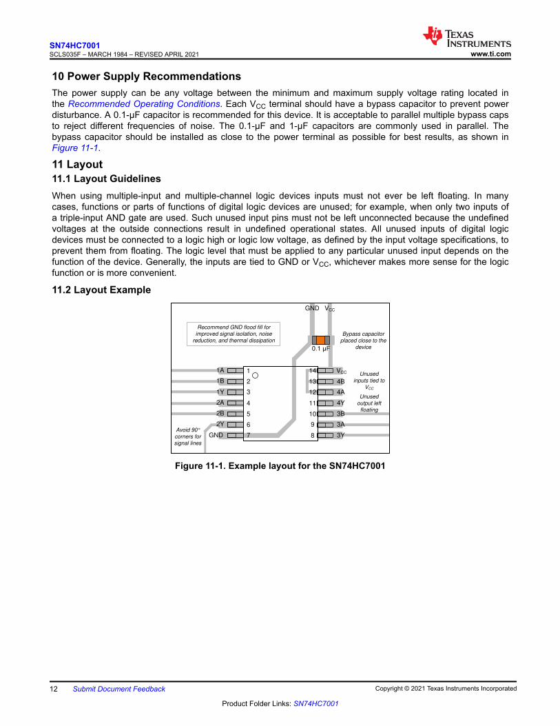
10 Power Supply RecommendationsThe power supply can be any voltage between the minimum and maximum supply voltage rating located inthe Recommended Operating Conditions. Each VCC terminal should have a bypass capacitor to prevent powerdisturbance. A 0.1-μF capacitor is recommended for this device. It is acceptable to parallel multiple bypass capsto reject different frequencies of noise. The 0.1-μF and 1-μF capacitors are commonly used in parallel. Thebypass capacitor should be installed as close to the power terminal as possible for best results, as shown inFigure 11-1.
11 Layout11.1 Layout GuidelinesWhen using multiple-input and multiple-channel logic devices inputs must not ever be left floating. In manycases, functions or parts of functions of digital logic devices are unused; for example, when only two inputs ofa triple-input AND gate are used. Such unused input pins must not be left unconnected because the undefinedvoltages at the outside connections result in undefined operational states. All unused inputs of digital logicdevices must be connected to a logic high or logic low voltage, as defined by the input voltage specifications, toprevent them from floating. The logic level that must be applied to any particular unused input depends on thefunction of the device. Generally, the inputs are tied to GND or VCC, whichever makes more sense for the logicfunction or is more convenient.
11.2 Layout Example
1
2
3
4
5
6
7
14
13
12
11
10
9
8
1A
1B
2A
2B
2Y
GND VCC
4B
4A
3B
3A
3YGND
VCC
4Y
1Y
0.1 F
Unused
inputs tied to
VCC
Bypass capacitor
placed close to the
device
Avoid 90°
corners for
signal lines
Recommend GND flood fill for
improved signal isolation, noise
reduction, and thermal dissipation
Unused
output left
floating
Figure 11-1. Example layout for the SN74HC7001
SN74HC7001SCLS035F – MARCH 1984 – REVISED APRIL 2021 www.ti.com
12 Submit Document Feedback Copyright © 2021 Texas Instruments Incorporated
Product Folder Links: SN74HC7001
12 Device and Documentation Support12.1 Documentation Support12.1.1 Related Documentation
For related documentation see the following:• HCMOS Design Considerations• CMOS Power Consumption and CPD Calculation• Designing with Logic
12.2 Related LinksThe table below lists quick access links. Categories include technical documents, support and communityresources, tools and software, and quick access to sample or buy.
12.3 Support ResourcesTI E2E™ support forums are an engineer's go-to source for fast, verified answers and design help — straightfrom the experts. Search existing answers or ask your own question to get the quick design help you need.
Linked content is provided "AS IS" by the respective contributors. They do not constitute TI specifications and donot necessarily reflect TI's views; see TI's Terms of Use.
12.4 TrademarksTI E2E™ is a trademark of Texas Instruments.All trademarks are the property of their respective owners.12.5 Electrostatic Discharge Caution
This integrated circuit can be damaged by ESD. Texas Instruments recommends that all integrated circuits be handledwith appropriate precautions. Failure to observe proper handling and installation procedures can cause damage.ESD damage can range from subtle performance degradation to complete device failure. Precision integrated circuits maybe more susceptible to damage because very small parametric changes could cause the device not to meet its publishedspecifications.
12.6 GlossaryTI Glossary This glossary lists and explains terms, acronyms, and definitions.
13 Mechanical, Packaging, and Orderable InformationThe following pages include mechanical, packaging, and orderable information. This information is the mostcurrent data available for the designated devices. This data is subject to change without notice and revision ofthis document. For browser-based versions of this data sheet, refer to the left-hand navigation.
www.ti.comSN74HC7001
SCLS035F – MARCH 1984 – REVISED APRIL 2021
Copyright © 2021 Texas Instruments Incorporated Submit Document Feedback 13
Product Folder Links: SN74HC7001
PACKAGE OPTION ADDENDUM
www.ti.com 13-Aug-2021
Addendum-Page 1
PACKAGING INFORMATION
Orderable Device Status(1)
Package Type PackageDrawing
Pins PackageQty
Eco Plan(2)
Lead finish/Ball material
(6)
MSL Peak Temp(3)
Op Temp (°C) Device Marking(4/5)
Samples
SN74HC7001D ACTIVE SOIC D 14 50 RoHS & Green NIPDAU Level-1-260C-UNLIM -40 to 85 HC7001
SN74HC7001DG4 ACTIVE SOIC D 14 50 RoHS & Green NIPDAU Level-1-260C-UNLIM -40 to 85 HC7001
SN74HC7001DR ACTIVE SOIC D 14 2500 RoHS & Green NIPDAU | SN Level-1-260C-UNLIM -40 to 85 HC7001
SN74HC7001DT ACTIVE SOIC D 14 250 RoHS & Green NIPDAU Level-1-260C-UNLIM -40 to 85 HC7001
SN74HC7001N ACTIVE PDIP N 14 25 RoHS & Green NIPDAU N / A for Pkg Type -40 to 85 SN74HC7001N
(1) The marketing status values are defined as follows:ACTIVE: Product device recommended for new designs.LIFEBUY: TI has announced that the device will be discontinued, and a lifetime-buy period is in effect.NRND: Not recommended for new designs. Device is in production to support existing customers, but TI does not recommend using this part in a new design.PREVIEW: Device has been announced but is not in production. Samples may or may not be available.OBSOLETE: TI has discontinued the production of the device.
(2) RoHS: TI defines "RoHS" to mean semiconductor products that are compliant with the current EU RoHS requirements for all 10 RoHS substances, including the requirement that RoHS substancedo not exceed 0.1% by weight in homogeneous materials. Where designed to be soldered at high temperatures, "RoHS" products are suitable for use in specified lead-free processes. TI mayreference these types of products as "Pb-Free".RoHS Exempt: TI defines "RoHS Exempt" to mean products that contain lead but are compliant with EU RoHS pursuant to a specific EU RoHS exemption.Green: TI defines "Green" to mean the content of Chlorine (Cl) and Bromine (Br) based flame retardants meet JS709B low halogen requirements of <=1000ppm threshold. Antimony trioxide basedflame retardants must also meet the <=1000ppm threshold requirement.
(3) MSL, Peak Temp. - The Moisture Sensitivity Level rating according to the JEDEC industry standard classifications, and peak solder temperature.
(4) There may be additional marking, which relates to the logo, the lot trace code information, or the environmental category on the device.
(5) Multiple Device Markings will be inside parentheses. Only one Device Marking contained in parentheses and separated by a "~" will appear on a device. If a line is indented then it is a continuationof the previous line and the two combined represent the entire Device Marking for that device.
(6) Lead finish/Ball material - Orderable Devices may have multiple material finish options. Finish options are separated by a vertical ruled line. Lead finish/Ball material values may wrap to twolines if the finish value exceeds the maximum column width.
PACKAGE OPTION ADDENDUM
www.ti.com 13-Aug-2021
Addendum-Page 2
Important Information and Disclaimer:The information provided on this page represents TI's knowledge and belief as of the date that it is provided. TI bases its knowledge and belief on informationprovided by third parties, and makes no representation or warranty as to the accuracy of such information. Efforts are underway to better integrate information from third parties. TI has taken andcontinues to take reasonable steps to provide representative and accurate information but may not have conducted destructive testing or chemical analysis on incoming materials and chemicals.TI and TI suppliers consider certain information to be proprietary, and thus CAS numbers and other limited information may not be available for release.
In no event shall TI's liability arising out of such information exceed the total purchase price of the TI part(s) at issue in this document sold by TI to Customer on an annual basis.
TAPE AND REEL INFORMATION
*All dimensions are nominal
Device PackageType
PackageDrawing
Pins SPQ ReelDiameter
(mm)
ReelWidth
W1 (mm)
A0(mm)
B0(mm)
K0(mm)
P1(mm)
W(mm)
Pin1Quadrant
SN74HC7001DR SOIC D 14 2500 330.0 16.4 6.6 9.3 2.1 8.0 16.0 Q1
SN74HC7001DR SOIC D 14 2500 330.0 16.4 6.5 9.0 2.1 8.0 16.0 Q1
SN74HC7001DT SOIC D 14 250 330.0 16.4 6.5 9.0 2.1 8.0 16.0 Q1
PACKAGE MATERIALS INFORMATION
www.ti.com 18-Feb-2021
Pack Materials-Page 1
*All dimensions are nominal
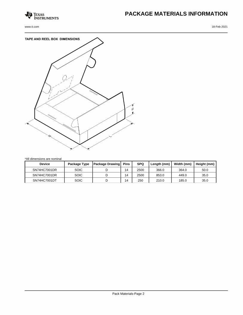
Device Package Type Package Drawing Pins SPQ Length (mm) Width (mm) Height (mm)
SN74HC7001DR SOIC D 14 2500 366.0 364.0 50.0
SN74HC7001DR SOIC D 14 2500 853.0 449.0 35.0
SN74HC7001DT SOIC D 14 250 210.0 185.0 35.0
PACKAGE MATERIALS INFORMATION
www.ti.com 18-Feb-2021
Pack Materials-Page 2
IMPORTANT NOTICE AND DISCLAIMERTI PROVIDES TECHNICAL AND RELIABILITY DATA (INCLUDING DATASHEETS), DESIGN RESOURCES (INCLUDING REFERENCEDESIGNS), APPLICATION OR OTHER DESIGN ADVICE, WEB TOOLS, SAFETY INFORMATION, AND OTHER RESOURCES “AS IS”AND WITH ALL FAULTS, AND DISCLAIMS ALL WARRANTIES, EXPRESS AND IMPLIED, INCLUDING WITHOUT LIMITATION ANYIMPLIED WARRANTIES OF MERCHANTABILITY, FITNESS FOR A PARTICULAR PURPOSE OR NON-INFRINGEMENT OF THIRDPARTY INTELLECTUAL PROPERTY RIGHTS.These resources are intended for skilled developers designing with TI products. You are solely responsible for (1) selecting the appropriateTI products for your application, (2) designing, validating and testing your application, and (3) ensuring your application meets applicablestandards, and any other safety, security, or other requirements. These resources are subject to change without notice. TI grants youpermission to use these resources only for development of an application that uses the TI products described in the resource. Otherreproduction and display of these resources is prohibited. No license is granted to any other TI intellectual property right or to any third partyintellectual property right. TI disclaims responsibility for, and you will fully indemnify TI and its representatives against, any claims, damages,costs, losses, and liabilities arising out of your use of these resources.TI’s products are provided subject to TI’s Terms of Sale (https:www.ti.com/legal/termsofsale.html) or other applicable terms available eitheron ti.com or provided in conjunction with such TI products. TI’s provision of these resources does not expand or otherwise alter TI’sapplicable warranties or warranty disclaimers for TI products.IMPORTANT NOTICE
Mailing Address: Texas Instruments, Post Office Box 655303, Dallas, Texas 75265Copyright © 2021, Texas Instruments Incorporated