Embed Size (px)
Citation preview

2A 2Y
2OE
1A 1Y
1OE
4A 4Y
4OE
3A 3Y
3OE
Product
Folder
Sample &Buy
Technical
Documents
Tools &
Software
Support &Community
An IMPORTANT NOTICE at the end of this data sheet addresses availability, warranty, changes, use in safety-critical applications,intellectual property matters and other important disclaimers. PRODUCTION DATA.
SN74LV125ASCES124N –DECEMBER 1997–REVISED JANUARY 2016
SN74LV125A Quadruple Bus Buffer Gates With 3-State Outputs
1
1 Features1• 2-V to 5.5-V VCC Operation• Max tpd of 6 ns at 5 V• Typical VOLP (Output Ground Bounce)
< 0.8 V at VCC = 3.3 V, TA = 25°C• Typical VOHV (Output VOH Undershoot)
> 2.3 V at VCC = 3.3 V, TA = 25°C• Support Mixed-Mode Voltage Operation on
All Ports• Ioff Supports Partial-Power-Down Mode Operation• Latch-Up Performance Exceeds 250 mA Per
JESD 17• ESD Protection Exceeds JESD 22
– 4000-V Human-Body Model– 200-V Machine Model– 2000-V Charged-Device Model
2 Applications• Flow Meters• Solid State Drives (SSDs): Enterprise• Power Over Ethernet (PoE)• Programmable Logic Controllers• Motor Drives and Controls• Electronic Points of Sale
3 DescriptionThe SN74LV125A quadruple bus buffer gate isdesigned for 2-V to 5.5-V VCC operation.
Device Information(1)
PART NUMBER PACKAGE BODY SIZE (NOM)
SN74LV125A
TVSOP (14) 3.60 mm x 4.40 mmSOIC (14) 8.65 mm × 3.91 mmSOP (14) 10.30mm x 5.30 mmSSOP (14) 6.20 mm x 5.30 mmTSSOP (14) 5.00 mm x 4.40 mm
(1) For all available packages, see the orderable addendum atthe end of the data sheet.
4 Simplified Schematic

2
SN74LV125ASCES124N –DECEMBER 1997–REVISED JANUARY 2016 www.ti.com
Product Folder Links: SN74LV125A
Submit Documentation Feedback Copyright © 1997–2016, Texas Instruments Incorporated
Table of Contents1 Features .................................................................. 12 Applications ........................................................... 13 Description ............................................................. 14 Simplified Schematic............................................. 15 Revision History..................................................... 26 Pin Configuration and Functions ......................... 37 Specifications......................................................... 4
7.1 Absolute Maximum Ratings ...................................... 47.2 ESD Ratings ............................................................ 47.3 Recommended Operating Conditions....................... 57.4 Thermal Information .................................................. 57.5 Electrical Characteristics........................................... 67.6 Switching Characteristics, VCC = 2.5 V ± 0.2 V ........ 67.7 Switching Characteristics, VCC = 3.3 V ± 0.3 V ....... 67.8 Switching Characteristics, VCC = 5 V ± 0.5 V ........... 77.9 Noise Characteristics ................................................ 77.10 Operating Characteristics........................................ 77.11 Typical Characteristics ............................................ 7
8 Parameter Measurement Information .................. 8
9 Detailed Description .............................................. 99.1 Overview ................................................................... 99.2 Functional Block Diagram ......................................... 99.3 Feature Description................................................... 99.4 Device Functional Modes.......................................... 9
10 Application and Implementation........................ 1010.1 Application Information.......................................... 1010.2 Typical Application ............................................... 10
11 Power Supply Recommendations ..................... 1112 Layout................................................................... 12
12.1 Layout Guidelines ................................................. 1212.2 Layout Example .................................................... 12
13 Device and Documentation Support ................. 1213.1 Related Links ........................................................ 1213.2 Trademarks ........................................................... 1213.3 Electrostatic Discharge Caution............................ 1213.4 Glossary ................................................................ 12
14 Mechanical, Packaging, and OrderableInformation ........................................................... 12
5 Revision History
Changes from Revision M (December 2014) to Revision N Page
• Added Tj spec to Absolute Maximum Ratings table ............................................................................................................... 4• Added text to Overview section ............................................................................................................................................. 9
Changes from Revision L (April 2005) to Revision M Page
• Added Applications, Device Information table, Pin Functions table, ESD Ratings table, Thermal Information table,Typical Characteristics, Feature Description section, Device Functional Modes, Application and Implementationsection, Power Supply Recommendations section, Layout section, Device and Documentation Support section, andMechanical, Packaging, and Orderable Information section. ................................................................................................. 1
• Deleted Ordering Information table. ....................................................................................................................................... 1• Changed MAX operating temperature to 125°C in Recommended Operating Conditions table. ......................................... 5

1
2
3
4
5
6
7
14
13
12
11
10
9
8
1OE
1A
1Y
2OE
2A
2Y
GND
VCC
4OE
4A
4Y
3OE
3A
3Y
SN74LV125A . . . D, DB, DGV, N, NS,
OR PW PACKAGE
(TOP VIEW)
SN74LV125A . . . RGY PACKAGE
(TOP VIEW)
1 14
7 8
2
3
4
5
6
13
12
11
10
9
4OE
4A
4Y
3OE
3A
1A
1Y
2OE
2A
2Y
1O
E
3Y
V
GN
D
CC
3
SN74LV125Awww.ti.com SCES124N –DECEMBER 1997–REVISED JANUARY 2016
Product Folder Links: SN74LV125A
Submit Documentation FeedbackCopyright © 1997–2016, Texas Instruments Incorporated
6 Pin Configuration and Functions
Pin FunctionsPIN
TYPE DESCRIPTIONNO. NAME1 1OE I Output Enable 12 1A I 1A Input3 1Y O 1Y Output4 2OE I Output Enable 25 2A I 2A Input6 2Y O 2Y Output7 GND — Ground Pin8 3Y O 3Y Output9 3A I 3A Input10 3OE I Output Enable 311 4Y O 4Y Output12 4A I 4A Input13 4OE I Output Enable 414 VCC — Power Pin

4
SN74LV125ASCES124N –DECEMBER 1997–REVISED JANUARY 2016 www.ti.com
Product Folder Links: SN74LV125A
Submit Documentation Feedback Copyright © 1997–2016, Texas Instruments Incorporated
(1) Stresses beyond those listed under Absolute Maximum Ratings may cause permanent damage to the device. These are stress ratingsonly, and functional operation of the device at these or any other conditions beyond those indicated under Recommended OperatingConditions is not implied. Exposure to absolute-maximum-rated conditions for extended periods may affect device reliability.
(2) The input and output negative-voltage ratings may be exceeded if the input and output current ratings are observed.(3) This value is limited to 5.5-V maximum.
7 Specifications
7.1 Absolute Maximum Ratings (1)
over operating free-air temperature range (unless otherwise noted)MIN MAX UNIT
VCC Supply voltage –0.5 7 VVI Input voltage range (2) –0.5 7 VVO Voltage range applied to any output in the high-impedance or power-off state (2) –0.5 7 VVO Output voltage range (2) (3) –0.5 VCC + 0.5 VIIK Input clamp current VI < 0 –20 mAIOK Output clamp current VO < 0 –50 mAIO Continuous output current VO = 0 to VCC ±35 mA
Continuous current through VCC or GND ±70 mATj Junction temperature 150 °CTstg Storage temperature –65 150 °C
(1) JEDEC document JEP155 states that 500-V HBM allows safe manufacturing with a standard ESD control process.(2) JEDEC document JEP157 states that 250-V CDM allows safe manufacturing with a standard ESD control process.
7.2 ESD RatingsMAX UNIT
V(ESD) Electrostatic discharge
Human body model (HBM), per ANSI/ESDA/JEDEC JS-001, all pins (1) 4000
VCharged device model (CDM), per JEDEC specification JESD22-C101,all pins (2) 2000
Machine Model (MM) 200

5
SN74LV125Awww.ti.com SCES124N –DECEMBER 1997–REVISED JANUARY 2016
Product Folder Links: SN74LV125A
Submit Documentation FeedbackCopyright © 1997–2016, Texas Instruments Incorporated
(1) All unused inputs of the device must be held at VCC or GND to ensure proper device operation. Refer to the TI application report,Implications of Slow or Floating CMOS Inputs (SCBA004).
7.3 Recommended Operating Conditionsover operating free-air temperature range (unless otherwise noted) (1)
SN74LV125AUNIT
MIN MAXVCC Supply voltage 2 5.5 V
VIH High-level input voltage
VCC = 2 V 1.5
VVCC = 2.3 V to 2.7 V VCC × 0.7VCC = 3 V to 3.6 V VCC × 0.7VCC = 4.5 V to 5.5 V VCC × 0.7
VIL Low-level input voltage
VCC = 2 V 0.5
VVCC = 2.3 V to 2.7 V VCC × 0.3VCC = 3 V to 3.6 V VCC × 0.3VCC = 4.5 V to 5.5 V VCC × 0.3
VI Input voltage 0 5.5 V
VO Output voltageHigh or low state 0 VCC V3-state 0 5.5
IOH High-level output current
VCC = 2 V –50 µAVCC = 2.3 V to 2.7 V –2
mAVCC = 3 V to 3.6 V –8VCC = 4.5 V to 5.5 V –16
IOL Low-level output current
VCC = 2 V 50 µAVCC = 2.3 V to 2.7 V 2
mAVCC = 3 V to 3.6 V 8VCC = 4.5 V to 5.5 V 16
∆t/∆v Input transition rise or fall rateVCC = 2.3 V to 2.7 V 200
ns/VVCC = 3 V to 3.6 V 100VCC = 4.5 V to 5.5 V 20
TA Operating free-air temperature –40 125 °C
(1) For more information about traditional and new thermal metrics, see the IC Package Thermal Metrics application report (SPRA953).
7.4 Thermal Information
THERMAL METRIC (1)SN74LV125A
UNITD DB DGV N NS PW RGY14 PINS
RθJAJunction-to-ambient thermalresistance 92.7 105.0 127.6 89.2 89.6 119.8 55.0
°C/W
RθJC(top)Junction-to-case (top) thermalresistance 54.1 57.5 50.7 47.0 47.2 48.6 67.4
RθJB Junction-to-board thermal resistance 47.0 52.3 60.5 47.9 48.4 61.5 31.0
ψJTJunction-to-top characterizationparameter 18.9 19.1 6.1 14.1 14.0 5.7 2.6
ψJBJunction-to-board characterizationparameter 46.7 51.8 59.8 47.5 48.1 61.0 31.1
RθJC(bot)Junction-to-case (bottom) thermalresistance — — — — — — 11.6

6
SN74LV125ASCES124N –DECEMBER 1997–REVISED JANUARY 2016 www.ti.com
Product Folder Links: SN74LV125A
Submit Documentation Feedback Copyright © 1997–2016, Texas Instruments Incorporated
7.5 Electrical Characteristicsover recommended operating free-air temperature range (unless otherwise noted)
PARAMETER TEST CONDITIONS VCCTA = 25°C –40°C to 85°C –40°C to 125°C
UNITMIN TYP MAX MIN MAX MIN MAX
VOH
IOH = –50 µA 2 V to5.5 V
VCC – 0.1 VCC – 0.1 VCC – 0.1
VIOH = –2 mA 2.3 V 2 2 2IOH = –8 mA 3 V 2.48 2.48 2.48IOH = –16 mA 4.5 V 3.8 3.8 3.8
VOL
IOL = 50 µA 2 V to5.5 V 0.1 0.1 0.1
VIOL = 2 mA 2.3 V 0.4 0.4 0.4IOL = 8 mA 3 V 0.44 0.44 0.44IOL = 16 mA 4.5 V 0.55 0.55 0.55
II VI = 5.5 V or GND 0 to5.5 V ±1 ±1 ±1 µA
IOZ VO = VCC or GND 5.5 V ±5 ±5 ±5 µAICC VI = VCC or GND, IO = 0 5.5 V 20 20 20 µA
IoffVI or VO = 0 to 5.5V 0 5 5 5 µA
Ci VI = VCC or GND3.3 V 1.6
pF5 V 1.6
(1) On products compliant to MIL-PRF-38535, this parameter is not production tested.
7.6 Switching Characteristics, VCC = 2.5 V ± 0.2 Vover recommended operating free-air temperature range (unless otherwise noted) (see Figure 3)
PARAMETER FROM(INPUT)
TO(OUTPUT)
LOADCAPACITANCE
TA = 25°C –40°C to 85°C –40°C to 125°CUNIT
MIN TYP MAX MIN MAX MIN MAXtpd A Y
CL = 15 pF6.8 (1) 13 (1) 1 15.5 1 17
nsten OE Y 7 (1) 13 (1) 1 15.5 1 17tdis OE Y 5.1 (1) 14.7 (1) 1 17 1 18tpd A Y
CL = 50 pF
8.7 16.5 1 18.5 1 20
nsten OE Y 8.8 16.5 1 18.5 1 20tdis OE Y 7.3 18.2 1 20.5 1 21.5
tsk(o) 2 2 2
(1) On products compliant to MIL-PRF-38535, this parameter is not production tested.
7.7 Switching Characteristics, VCC = 3.3 V ± 0.3 Vover recommended operating free-air temperature range(unless otherwise noted) (see Figure 3)
PARAMETER FROM(INPUT)
TO(OUTPUT)
LOADCAPACITANCE
TA = 25°C –40°C to 85°C –40°C to 125°CUNIT
MIN TYP MAX MIN MAX MIN MAXtpd A Y
CL = 15 pF4.8 (1) 8 (1) 1 9.5 1 11
nsten OE Y 4.8 (1) 8 (1) 1 9.5 1 10.5tdis OE Y 4.1 (1) 9.7 (1) 1 11.5 1 12.5tpd A Y
CL = 50 pF
6.1 11.5 1 13 1 14.5
nsten OE Y 6.2 11.5 1 13 1 14tdis OE Y 5.5 13.2 1 15 1 16
tsk(o) 1.5 1.5 1.5

Temperature (qC)
TP
D (
ns)
-100 -50 0 50 100 1500
1
2
3
4
5
6
7
D001
TPD in ns
VCC
TP
D (
ns)
0 1 2 3 4 5 60
1
2
3
4
5
6
7
8
D002
TPD in ns
7
SN74LV125Awww.ti.com SCES124N –DECEMBER 1997–REVISED JANUARY 2016
Product Folder Links: SN74LV125A
Submit Documentation FeedbackCopyright © 1997–2016, Texas Instruments Incorporated
(1) On products compliant to MIL-PRF-38535, this parameter is not production tested.
7.8 Switching Characteristics, VCC = 5 V ± 0.5 Vover recommended operating free-air temperature range (unless otherwise noted) (see Figure 3)
PARAMETER FROM(INPUT)
TO(OUTPUT)
LOADCAPACITANCE
TA = 25°C –40°C to 85°C –40°C to 125°CUNIT
MIN TYP MAX MIN MAX MIN MAXtpd A Y
CL = 15 pF3.4 (1) 5.5 (1) 1 6.5 1 7.5
nsten OE Y 3.4 (1) 5.1 (1) 1 6 1 7tdis OE Y 3.2 (1) 6.8 (1) 1 8 1 9tpd A Y
CL = 50 pF
4.3 7.5 1 8.5 1 9.5
nsten OE Y 4.4 7.1 1 8 1 9tdis OE Y 4 8.8 1 10 1 11
tsk(o) 1 1 1
(1) Characteristics are for surface-mount packages only.
7.9 Noise Characteristics (1)
VCC = 3.3 V, CL = 50 pF, TA = 25°C
PARAMETERSN74LV125A
UNITMIN TYP MAX
VOL(P) Quiet output, maximum dynamic VOL 0.4 0.8 VVOL(V) Quiet output, minimum dynamic VOL –0.3 –0.8 VVOH(V) Quiet output, minimum dynamic VOH 3 VVIH(D) High-level dynamic input voltage 2.31 VVIL(D) Low-level dynamic input voltage 0.99 V
7.10 Operating CharacteristicsTA = 25°C
PARAMETER TEST CONDITIONS VCC TYP UNIT
Cpd Power dissipation capacitance Outputs enabled CL = 50 pF, f = 10 MHz3.3 V 15.5
pF5 V 17.6
7.11 Typical Characteristics
Figure 1. TPD vs Temperature Figure 2. TPD vs VCC at 25°C

50% VCC
VCC
VCC
0 V
0 V
thtsu
VOLTAGE WAVEFORMS
SETUP AND HOLD TIMES
Data Input
tPLH
tPHL
tPHL
tPLH
VOH
VOH
VOL
VOL
VCC
0 V
50% VCC50% VCC
Input
Out-of-Phase
Output
In-Phase
Output
Timing Input
50% VCC
VOLTAGE WAVEFORMS
PROPAGATION DELAY TIMES
INVERTING AND NONINVERTING OUTPUTS
Output
Control
Output
Waveform 1
S1 at VCC(see Note B)
Output
Waveform 2
S1 at GND
(see Note B)
VOL
VOH
tPZL
tPZH
tPLZ
tPHZ
≈VCC
0 V
50% VCCVOL + 0.3 V
50% VCC≈0 V
VCC
VOLTAGE WAVEFORMS
ENABLE AND DISABLE TIMES
LOW- AND HIGH-LEVEL ENABLING
tPLH/tPHLtPLZ/tPZLtPHZ/tPZHOpen Drain
Open
VCCGND
VCC
TEST S1
VCC
0 V
50% VCC
tw
VOLTAGE WAVEFORMS
PULSE DURATION
Input
NOTES: A. CL includes probe and jig capacitance.
B. Waveform 1 is for an output with internal conditions such that the output is low, except when disabled by the output control.
Waveform 2 is for an output with internal conditions such that the output is high, except when disabled by the output control.
C. All input pulses are supplied by generators having the following characteristics: PRR ≤ 1 MHz, ZO = 50 Ω, tr ≤ 3 ns, tf ≤ 3 ns.
D. The outputs are measured one at a time, with one input transition per measurement.
E. tPLZ and tPHZ are the same as tdis.
F. tPZL and tPZH are the same as ten.
G. tPHL and tPLH are the same as tpd.
H. All parameters and waveforms are not applicable to all devices.
From Output
Under Test
CL(see Note A)
LOAD CIRCUIT FOR
3-STATE AND OPEN-DRAIN OUTPUTS
S1
VCC
RL = 1 kΩ
GNDFrom Output
Under Test
CL(see Note A)
Test
Point
LOAD CIRCUIT FOR
TOTEM-POLE OUTPUTS
Open
50% VCC
50% VCC 50% VCC
50% VCC
50% VCC 50% VCC
50% VCC 50% VCC
VOH − 0.3 V
8
SN74LV125ASCES124N –DECEMBER 1997–REVISED JANUARY 2016 www.ti.com
Product Folder Links: SN74LV125A
Submit Documentation Feedback Copyright © 1997–2016, Texas Instruments Incorporated
8 Parameter Measurement Information
Figure 3. Load Circuit And Voltage Waveforms

2A 2Y
2OE
1A 1Y
1OE
4A 4Y
4OE
3A 3Y
3OE
9
SN74LV125Awww.ti.com SCES124N –DECEMBER 1997–REVISED JANUARY 2016
Product Folder Links: SN74LV125A
Submit Documentation FeedbackCopyright © 1997–2016, Texas Instruments Incorporated
9 Detailed Description
9.1 OverviewThe SN74LV125A quadruple bus buffer gate is designed for 2-V to 5.5-V VCC operation.
These devices feature independent line drivers with 3-state outputs. Each output is disabled when the associatedoutput-enable (OE) input is high.
To ensure the high-impedance state during power up or power down, tie OE to VCC through a pullup resistor; theminimum value of the resistor is determined by the current-sinking capability of the driver.
9.2 Functional Block Diagram
Figure 4. Logic Diagram (Positive Logic)
9.3 Feature Description• Wide operating voltage range
– Operates from 2 V to 5.5 V• Allows down-voltage translation
– Inputs accept voltages to 5.5 V• Ioff Feature
– Supports Live Insertion, Partial Power-Down Mode, and Back-Drive Protection
9.4 Device Functional Modes
Table 1. Function Table(Each Buffer)
INPUTS OUTPUTYOE A
L H HL L LH X Z
1OE
V
GND
5-V system
CC
µC orSystem Logic
µCSystem Logic
LEDs
Regulated 3.3 V or 5 V
1A
4A
1Y
4Y
4OE
10
SN74LV125ASCES124N –DECEMBER 1997–REVISED JANUARY 2016 www.ti.com
Product Folder Links: SN74LV125A
Submit Documentation Feedback Copyright © 1997–2016, Texas Instruments Incorporated
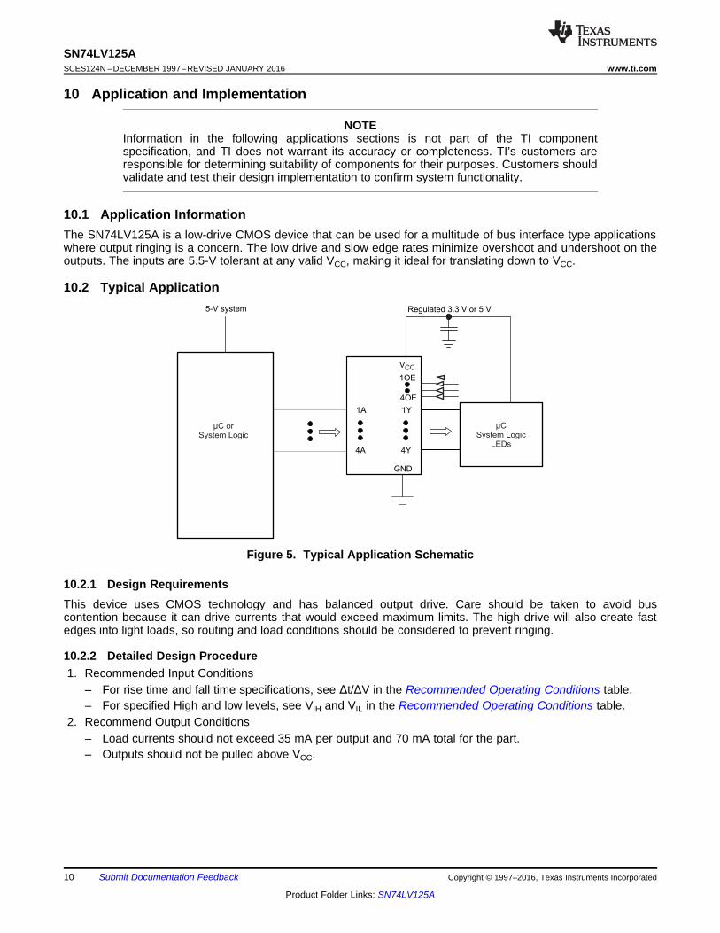
10 Application and Implementation
NOTEInformation in the following applications sections is not part of the TI componentspecification, and TI does not warrant its accuracy or completeness. TI’s customers areresponsible for determining suitability of components for their purposes. Customers shouldvalidate and test their design implementation to confirm system functionality.
10.1 Application InformationThe SN74LV125A is a low-drive CMOS device that can be used for a multitude of bus interface type applicationswhere output ringing is a concern. The low drive and slow edge rates minimize overshoot and undershoot on theoutputs. The inputs are 5.5-V tolerant at any valid VCC, making it ideal for translating down to VCC.
10.2 Typical Application
Figure 5. Typical Application Schematic
10.2.1 Design RequirementsThis device uses CMOS technology and has balanced output drive. Care should be taken to avoid buscontention because it can drive currents that would exceed maximum limits. The high drive will also create fastedges into light loads, so routing and load conditions should be considered to prevent ringing.
10.2.2 Detailed Design Procedure1. Recommended Input Conditions
– For rise time and fall time specifications, see Δt/ΔV in the Recommended Operating Conditions table.– For specified High and low levels, see VIH and VIL in the Recommended Operating Conditions table.
2. Recommend Output Conditions– Load currents should not exceed 35 mA per output and 70 mA total for the part.– Outputs should not be pulled above VCC.

11
SN74LV125Awww.ti.com SCES124N –DECEMBER 1997–REVISED JANUARY 2016
Product Folder Links: SN74LV125A
Submit Documentation FeedbackCopyright © 1997–2016, Texas Instruments Incorporated
Typical Application (continued)10.2.3 Application Curves
Figure 6. Switching Characteristics Comparison
11 Power Supply RecommendationsThe power supply can be any voltage between the MIN and MAX supply voltage rating located in theRecommended Operating Conditions table.
Each VCC pin should have a good bypass capacitor to prevent power disturbance. For devices with a singlesupply, 0.1 μF is recommended. If there are multiple VCC pins, 0.01 μF or 0.022 μF is recommended for eachpower pin. It is acceptable to parallel multiple bypass caps to reject different frequencies of noise. A 0.1 μF and1 μF are commonly used in parallel. The bypass capacitor should be installed as close to the power pin aspossible for best results.

Vcc
Unused Input
Input
Output
Input
Unused Input Output
12
SN74LV125ASCES124N –DECEMBER 1997–REVISED JANUARY 2016 www.ti.com
Product Folder Links: SN74LV125A
Submit Documentation Feedback Copyright © 1997–2016, Texas Instruments Incorporated
12 Layout
12.1 Layout GuidelinesWhen using multiple bit logic devices, inputs should not float. In many cases, functions or parts of functions ofdigital logic devices are unused. Some examples are when only two inputs of a triple-input AND gate are used,or when only 3 of the 4-buffer gates are used. Such input pins should not be left unconnected because theundefined voltages at the outside connections result in undefined operational states.
Specified in Figure 7 are rules that must be observed under all circumstances. All unused inputs of digital logicdevices must be connected to a high or low bias to prevent them from floating. The logic level that should beapplied to any particular unused input depends on the function of the device. Generally they will be tied to GNDor VCC, whichever makes more sense or is more convenient. It is acceptable to float outputs unless the part is atransceiver. If the transceiver has an output enable pin, it will disable the outputs section of the part whenasserted. This will not disable the input section of the I/Os so they also cannot float when disabled.
12.2 Layout Example
Figure 7. Layout Diagram
13 Device and Documentation Support
13.1 Related LinksThe table below lists quick access links. Categories include technical documents, support and communityresources, tools and software, and quick access to sample or buy.
Table 2. Related Links
PARTS PRODUCT FOLDER SAMPLE & BUY TECHNICALDOCUMENTS
TOOLS &SOFTWARE
SUPPORT &COMMUNITY
SN74LV125A Click here Click here Click here Click here Click here
13.2 TrademarksAll trademarks are the property of their respective owners.
13.3 Electrostatic Discharge CautionThese devices have limited built-in ESD protection. The leads should be shorted together or the device placed in conductive foamduring storage or handling to prevent electrostatic damage to the MOS gates.
13.4 GlossarySLYZ022 — TI Glossary.
This glossary lists and explains terms, acronyms, and definitions.
14 Mechanical, Packaging, and Orderable InformationThe following pages include mechanical, packaging, and orderable information. This information is the mostcurrent data available for the designated devices. This data is subject to change without notice and revision ofthis document. For browser-based versions of this data sheet, refer to the left-hand navigation.
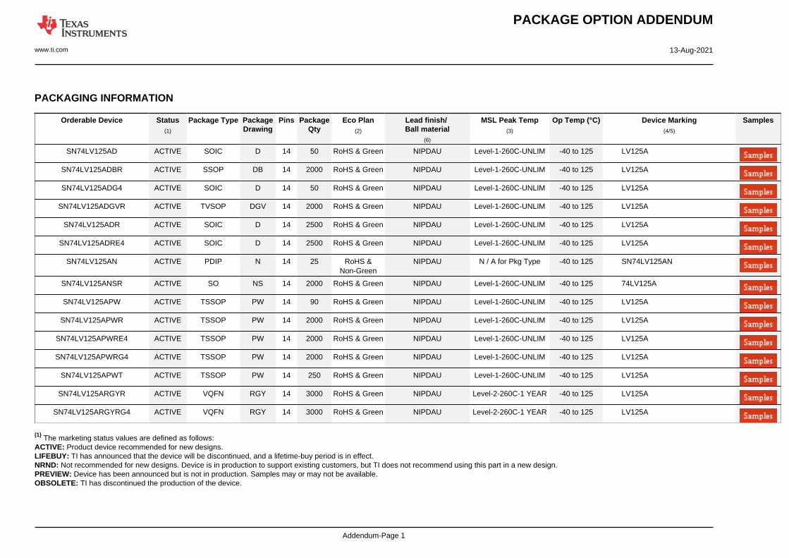
PACKAGE OPTION ADDENDUM
www.ti.com 13-Aug-2021
Addendum-Page 1
PACKAGING INFORMATION
Orderable Device Status(1)
Package Type PackageDrawing
Pins PackageQty
Eco Plan(2)
Lead finish/Ball material
(6)
MSL Peak Temp(3)
Op Temp (°C) Device Marking(4/5)
Samples
SN74LV125AD ACTIVE SOIC D 14 50 RoHS & Green NIPDAU Level-1-260C-UNLIM -40 to 125 LV125A
SN74LV125ADBR ACTIVE SSOP DB 14 2000 RoHS & Green NIPDAU Level-1-260C-UNLIM -40 to 125 LV125A
SN74LV125ADG4 ACTIVE SOIC D 14 50 RoHS & Green NIPDAU Level-1-260C-UNLIM -40 to 125 LV125A
SN74LV125ADGVR ACTIVE TVSOP DGV 14 2000 RoHS & Green NIPDAU Level-1-260C-UNLIM -40 to 125 LV125A
SN74LV125ADR ACTIVE SOIC D 14 2500 RoHS & Green NIPDAU Level-1-260C-UNLIM -40 to 125 LV125A
SN74LV125ADRE4 ACTIVE SOIC D 14 2500 RoHS & Green NIPDAU Level-1-260C-UNLIM -40 to 125 LV125A
SN74LV125AN ACTIVE PDIP N 14 25 RoHS &Non-Green
NIPDAU N / A for Pkg Type -40 to 125 SN74LV125AN
SN74LV125ANSR ACTIVE SO NS 14 2000 RoHS & Green NIPDAU Level-1-260C-UNLIM -40 to 125 74LV125A
SN74LV125APW ACTIVE TSSOP PW 14 90 RoHS & Green NIPDAU Level-1-260C-UNLIM -40 to 125 LV125A
SN74LV125APWR ACTIVE TSSOP PW 14 2000 RoHS & Green NIPDAU Level-1-260C-UNLIM -40 to 125 LV125A
SN74LV125APWRE4 ACTIVE TSSOP PW 14 2000 RoHS & Green NIPDAU Level-1-260C-UNLIM -40 to 125 LV125A
SN74LV125APWRG4 ACTIVE TSSOP PW 14 2000 RoHS & Green NIPDAU Level-1-260C-UNLIM -40 to 125 LV125A
SN74LV125APWT ACTIVE TSSOP PW 14 250 RoHS & Green NIPDAU Level-1-260C-UNLIM -40 to 125 LV125A
SN74LV125ARGYR ACTIVE VQFN RGY 14 3000 RoHS & Green NIPDAU Level-2-260C-1 YEAR -40 to 125 LV125A
SN74LV125ARGYRG4 ACTIVE VQFN RGY 14 3000 RoHS & Green NIPDAU Level-2-260C-1 YEAR -40 to 125 LV125A
(1) The marketing status values are defined as follows:ACTIVE: Product device recommended for new designs.LIFEBUY: TI has announced that the device will be discontinued, and a lifetime-buy period is in effect.NRND: Not recommended for new designs. Device is in production to support existing customers, but TI does not recommend using this part in a new design.PREVIEW: Device has been announced but is not in production. Samples may or may not be available.OBSOLETE: TI has discontinued the production of the device.
PACKAGE OPTION ADDENDUM
www.ti.com 13-Aug-2021
Addendum-Page 2
(2) RoHS: TI defines "RoHS" to mean semiconductor products that are compliant with the current EU RoHS requirements for all 10 RoHS substances, including the requirement that RoHS substancedo not exceed 0.1% by weight in homogeneous materials. Where designed to be soldered at high temperatures, "RoHS" products are suitable for use in specified lead-free processes. TI mayreference these types of products as "Pb-Free".RoHS Exempt: TI defines "RoHS Exempt" to mean products that contain lead but are compliant with EU RoHS pursuant to a specific EU RoHS exemption.Green: TI defines "Green" to mean the content of Chlorine (Cl) and Bromine (Br) based flame retardants meet JS709B low halogen requirements of <=1000ppm threshold. Antimony trioxide basedflame retardants must also meet the <=1000ppm threshold requirement.
(3) MSL, Peak Temp. - The Moisture Sensitivity Level rating according to the JEDEC industry standard classifications, and peak solder temperature.
(4) There may be additional marking, which relates to the logo, the lot trace code information, or the environmental category on the device.
(5) Multiple Device Markings will be inside parentheses. Only one Device Marking contained in parentheses and separated by a "~" will appear on a device. If a line is indented then it is a continuationof the previous line and the two combined represent the entire Device Marking for that device.
(6) Lead finish/Ball material - Orderable Devices may have multiple material finish options. Finish options are separated by a vertical ruled line. Lead finish/Ball material values may wrap to twolines if the finish value exceeds the maximum column width.
Important Information and Disclaimer:The information provided on this page represents TI's knowledge and belief as of the date that it is provided. TI bases its knowledge and belief on informationprovided by third parties, and makes no representation or warranty as to the accuracy of such information. Efforts are underway to better integrate information from third parties. TI has taken andcontinues to take reasonable steps to provide representative and accurate information but may not have conducted destructive testing or chemical analysis on incoming materials and chemicals.TI and TI suppliers consider certain information to be proprietary, and thus CAS numbers and other limited information may not be available for release.
In no event shall TI's liability arising out of such information exceed the total purchase price of the TI part(s) at issue in this document sold by TI to Customer on an annual basis.
OTHER QUALIFIED VERSIONS OF SN74LV125A :
• Automotive : SN74LV125A-Q1
NOTE: Qualified Version Definitions:
• Automotive - Q100 devices qualified for high-reliability automotive applications targeting zero defects
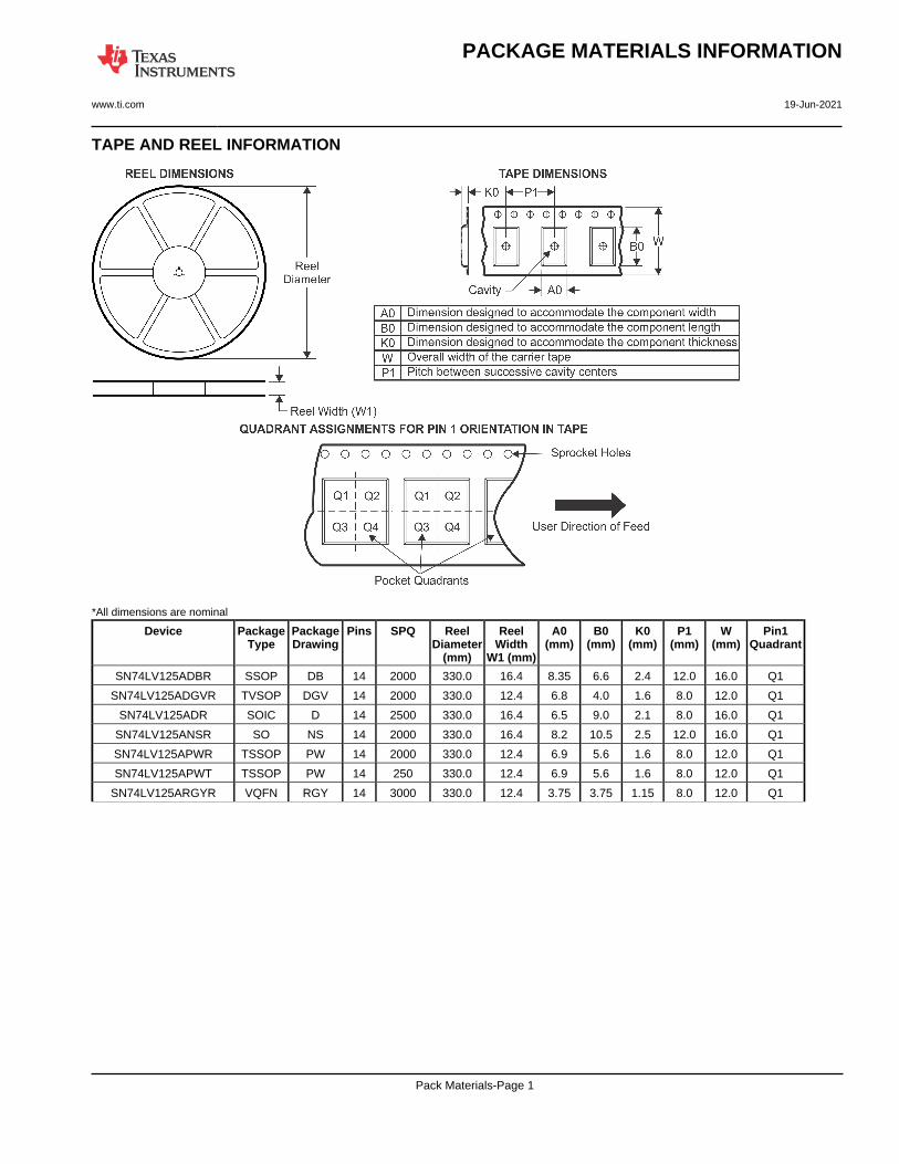
TAPE AND REEL INFORMATION
*All dimensions are nominal
Device PackageType
PackageDrawing
Pins SPQ ReelDiameter
(mm)
ReelWidth
W1 (mm)
A0(mm)
B0(mm)
K0(mm)
P1(mm)
W(mm)
Pin1Quadrant
SN74LV125ADBR SSOP DB 14 2000 330.0 16.4 8.35 6.6 2.4 12.0 16.0 Q1
SN74LV125ADGVR TVSOP DGV 14 2000 330.0 12.4 6.8 4.0 1.6 8.0 12.0 Q1
SN74LV125ADR SOIC D 14 2500 330.0 16.4 6.5 9.0 2.1 8.0 16.0 Q1
SN74LV125ANSR SO NS 14 2000 330.0 16.4 8.2 10.5 2.5 12.0 16.0 Q1
SN74LV125APWR TSSOP PW 14 2000 330.0 12.4 6.9 5.6 1.6 8.0 12.0 Q1
SN74LV125APWT TSSOP PW 14 250 330.0 12.4 6.9 5.6 1.6 8.0 12.0 Q1
SN74LV125ARGYR VQFN RGY 14 3000 330.0 12.4 3.75 3.75 1.15 8.0 12.0 Q1
PACKAGE MATERIALS INFORMATION
www.ti.com 19-Jun-2021
Pack Materials-Page 1

*All dimensions are nominal
Device Package Type Package Drawing Pins SPQ Length (mm) Width (mm) Height (mm)
SN74LV125ADBR SSOP DB 14 2000 853.0 449.0 35.0
SN74LV125ADGVR TVSOP DGV 14 2000 853.0 449.0 35.0
SN74LV125ADR SOIC D 14 2500 853.0 449.0 35.0
SN74LV125ANSR SO NS 14 2000 853.0 449.0 35.0
SN74LV125APWR TSSOP PW 14 2000 853.0 449.0 35.0
SN74LV125APWT TSSOP PW 14 250 853.0 449.0 35.0
SN74LV125ARGYR VQFN RGY 14 3000 853.0 449.0 35.0
PACKAGE MATERIALS INFORMATION
www.ti.com 19-Jun-2021
Pack Materials-Page 2


MECHANICAL DATA
MPDS006C – FEBRUARY 1996 – REVISED AUGUST 2000
POST OFFICE BOX 655303 • DALLAS, TEXAS 75265
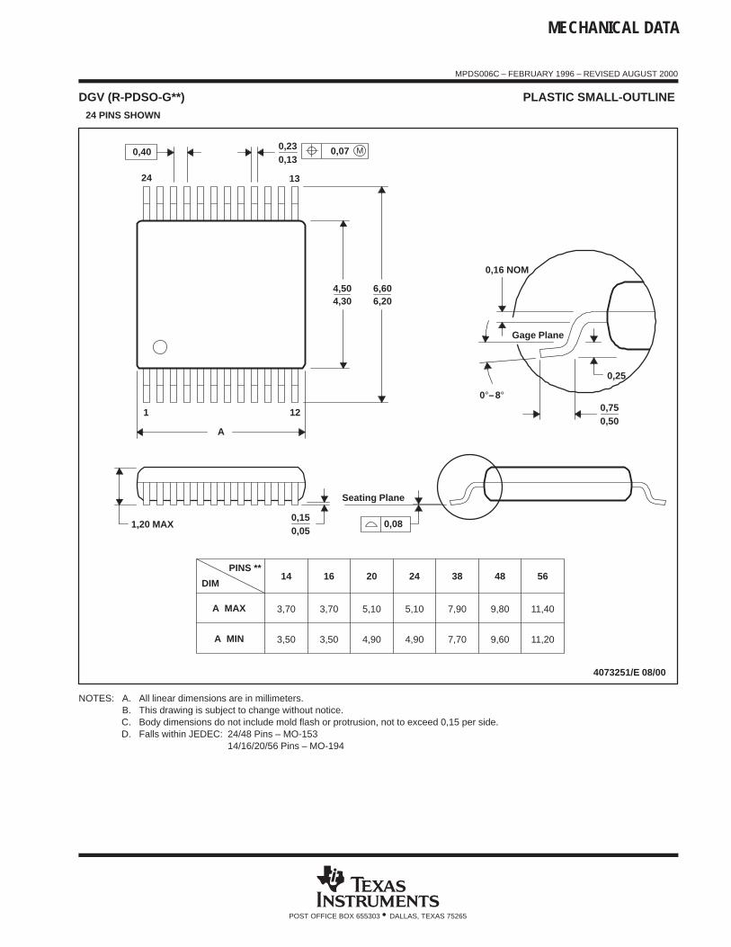
DGV (R-PDSO-G**) PLASTIC SMALL-OUTLINE 24 PINS SHOWN
14
3,70
3,50 4,90
5,10
20DIM
PINS **
4073251/E 08/00
1,20 MAX
Seating Plane
0,050,15
0,25
0,500,75
0,230,13
1 12
24 13
4,304,50
0,16 NOM
Gage Plane
A
7,90
7,70
382416
4,90
5,103,70
3,50
A MAX
A MIN
6,606,20
11,20
11,40
56
9,60
9,80
48
0,08
M0,070,40
0°–8°
NOTES: A. All linear dimensions are in millimeters.B. This drawing is subject to change without notice.C. Body dimensions do not include mold flash or protrusion, not to exceed 0,15 per side.D. Falls within JEDEC: 24/48 Pins – MO-153
14/16/20/56 Pins – MO-194


MECHANICAL DATA
MSSO002E – JANUARY 1995 – REVISED DECEMBER 2001
POST OFFICE BOX 655303 • DALLAS, TEXAS 75265
DB (R-PDSO-G**) PLASTIC SMALL-OUTLINE
4040065 /E 12/01
28 PINS SHOWN
Gage Plane
8,207,40
0,550,95
0,25
38
12,90
12,30
28
10,50
24
8,50
Seating Plane
9,907,90
30
10,50
9,90
0,38
5,605,00
15
0,22
14
A
28
1
2016
6,506,50
14
0,05 MIN
5,905,90
DIM
A MAX
A MIN
PINS **
2,00 MAX
6,90
7,50
0,65 M0,15
0°–8°
0,10
0,090,25
NOTES: A. All linear dimensions are in millimeters.B. This drawing is subject to change without notice.C. Body dimensions do not include mold flash or protrusion not to exceed 0,15.D. Falls within JEDEC MO-150
IMPORTANT NOTICE AND DISCLAIMERTI PROVIDES TECHNICAL AND RELIABILITY DATA (INCLUDING DATASHEETS), DESIGN RESOURCES (INCLUDING REFERENCEDESIGNS), APPLICATION OR OTHER DESIGN ADVICE, WEB TOOLS, SAFETY INFORMATION, AND OTHER RESOURCES “AS IS”AND WITH ALL FAULTS, AND DISCLAIMS ALL WARRANTIES, EXPRESS AND IMPLIED, INCLUDING WITHOUT LIMITATION ANYIMPLIED WARRANTIES OF MERCHANTABILITY, FITNESS FOR A PARTICULAR PURPOSE OR NON-INFRINGEMENT OF THIRDPARTY INTELLECTUAL PROPERTY RIGHTS.These resources are intended for skilled developers designing with TI products. You are solely responsible for (1) selecting the appropriateTI products for your application, (2) designing, validating and testing your application, and (3) ensuring your application meets applicablestandards, and any other safety, security, or other requirements. These resources are subject to change without notice. TI grants youpermission to use these resources only for development of an application that uses the TI products described in the resource. Otherreproduction and display of these resources is prohibited. No license is granted to any other TI intellectual property right or to any third partyintellectual property right. TI disclaims responsibility for, and you will fully indemnify TI and its representatives against, any claims, damages,costs, losses, and liabilities arising out of your use of these resources.TI’s products are provided subject to TI’s Terms of Sale (https:www.ti.com/legal/termsofsale.html) or other applicable terms available eitheron ti.com or provided in conjunction with such TI products. TI’s provision of these resources does not expand or otherwise alter TI’sapplicable warranties or warranty disclaimers for TI products.IMPORTANT NOTICE
Mailing Address: Texas Instruments, Post Office Box 655303, Dallas, Texas 75265Copyright © 2021, Texas Instruments Incorporated