Embed Size (px)
Citation preview
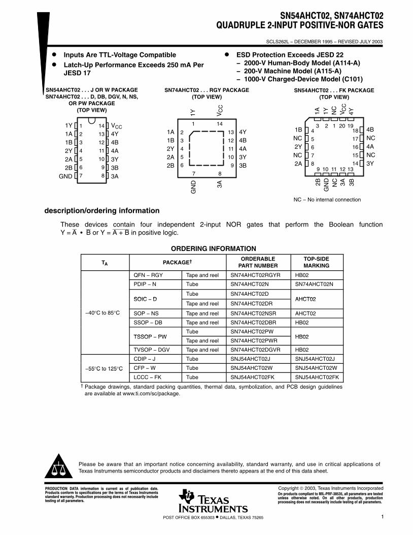
SN54AHCT02, SN74AHCT02QUADRUPLE 2-INPUT POSITIVE-NOR GATES
SCLS262L − DECEMBER 1995 − REVISED JULY 2003
1POST OFFICE BOX 655303 • DALLAS, TEXAS 75265
� Inputs Are TTL-Voltage Compatible
� Latch-Up Performance Exceeds 250 mA PerJESD 17
� ESD Protection Exceeds JESD 22− 2000-V Human-Body Model (A114-A)− 200-V Machine Model (A115-A)− 1000-V Charged-Device Model (C101)
1
2
3
4
5
6
7
14
13
12
11
10
9
8
1Y1A1B2Y2A2B
GND
VCC
4Y4B4A3Y3B3A
SN54AHCT02 . . . J OR W PACKAGESN74AHCT02 . . . D, DB, DGV, N, NS,
OR PW PACKAGE(TOP VIEW)
3 2 1 20 19
9 10 11 12 13
4
5
6
7
8
18
17
16
15
14
4BNC4ANC3Y
1BNC2YNC2A
1A 1Y NC
3A 3B
V 4Y
2BG
ND
NC
SN54AHCT02 . . . FK PACKAGE(TOP VIEW)
CC
NC − No internal connection
SN74AHCT02 . . . RGY PACKAGE(TOP VIEW)
1 14
7 8
2
3
4
5
6
13
12
11
10
9
4Y4B4A3Y3B
1A1B2Y2A2B
1Y
3AV
GN
D
CC
description/ordering information
These devices contain four independent 2-input NOR gates that perform the Boolean functionY = A � B or Y = A + B in positive logic.
ORDERING INFORMATION
TA PACKAGE† ORDERABLEPART NUMBER
TOP-SIDEMARKING
QFN − RGY Tape and reel SN74AHCT02RGYR HB02
PDIP − N Tube SN74AHCT02N SN74AHCT02N
SOIC DTube SN74AHCT02D
AHCT02SOIC − DTape and reel SN74AHCT02DR
AHCT02
−40°C to 85°C SOP − NS Tape and reel SN74AHCT02NSR AHCT02
SSOP − DB Tape and reel SN74AHCT02DBR HB02
TSSOP PWTube SN74AHCT02PW
HB02TSSOP − PWTape and reel SN74AHCT02PWR
HB02
TVSOP − DGV Tape and reel SN74AHCT02DGVR HB02
CDIP − J Tube SNJ54AHCT02J SNJ54AHCT02J
−55°C to 125°C CFP − W Tube SNJ54AHCT02W SNJ54AHCT02W55 C to 125 C
LCCC − FK Tube SNJ54AHCT02FK SNJ54AHCT02FK
† Package drawings, standard packing quantities, thermal data, symbolization, and PCB design guidelinesare available at www.ti.com/sc/package.
Copyright © 2003, Texas Instruments IncorporatedPRODUCTION DATA information is current as of publication date.Products conform to specifications per the terms of Texas Instrumentsstandard warranty. Production processing does not necessarily includetesting of all parameters.
Please be aware that an important notice concerning availability, standard warranty, and use in critical applications ofTexas Instruments semiconductor products and disclaimers thereto appears at the end of this data sheet.
On products compliant to MIL-PRF-38535, all parameters are testedunless otherwise noted. On all other products, productionprocessing does not necessarily include testing of all parameters.
SN54AHCT02, SN74AHCT02QUADRUPLE 2-INPUT POSITIVE-NOR GATES
SCLS262L − DECEMBER 1995 − REVISED JULY 2003
2 POST OFFICE BOX 655303 • DALLAS, TEXAS 75265
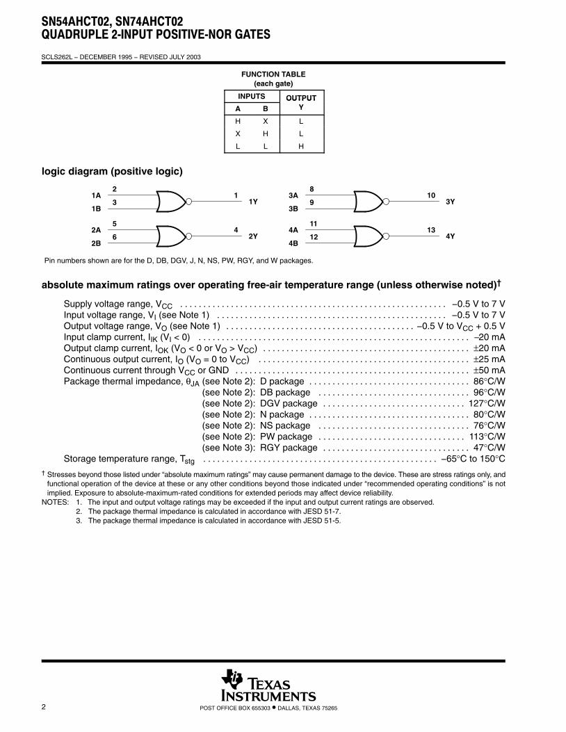
FUNCTION TABLE(each gate)
INPUTS OUTPUTA B
OUTPUTY
H X L
X H L
L L H
logic diagram (positive logic)
21A
31B
1Y1
83A
93B
3Y10
52A
62B
2Y4
114A
124B
4Y13
Pin numbers shown are for the D, DB, DGV, J, N, NS, PW, RGY, and W packages.
absolute maximum ratings over operating free-air temperature range (unless otherwise noted)†
Supply voltage range, VCC −0.5 V to 7 V. . . . . . . . . . . . . . . . . . . . . . . . . . . . . . . . . . . . . . . . . . . . . . . . . . . . . . . . . . Input voltage range, VI (see Note 1) −0.5 V to 7 V. . . . . . . . . . . . . . . . . . . . . . . . . . . . . . . . . . . . . . . . . . . . . . . . . . Output voltage range, VO (see Note 1) −0.5 V to VCC + 0.5 V. . . . . . . . . . . . . . . . . . . . . . . . . . . . . . . . . . . . . . . . . Input clamp current, IIK (VI < 0) −20 mA. . . . . . . . . . . . . . . . . . . . . . . . . . . . . . . . . . . . . . . . . . . . . . . . . . . . . . . . . . . Output clamp current, IOK (VO < 0 or VO > VCC) ±20 mA. . . . . . . . . . . . . . . . . . . . . . . . . . . . . . . . . . . . . . . . . . . . . Continuous output current, IO (VO = 0 to VCC) ±25 mA. . . . . . . . . . . . . . . . . . . . . . . . . . . . . . . . . . . . . . . . . . . . . . Continuous current through VCC or GND ±50 mA. . . . . . . . . . . . . . . . . . . . . . . . . . . . . . . . . . . . . . . . . . . . . . . . . . . Package thermal impedance, θJA (see Note 2): D package 86°C/W. . . . . . . . . . . . . . . . . . . . . . . . . . . . . . . . . . .
(see Note 2): DB package 96°C/W. . . . . . . . . . . . . . . . . . . . . . . . . . . . . . . . . (see Note 2): DGV package 127°C/W. . . . . . . . . . . . . . . . . . . . . . . . . . . . . . . (see Note 2): N package 80°C/W. . . . . . . . . . . . . . . . . . . . . . . . . . . . . . . . . . . (see Note 2): NS package 76°C/W. . . . . . . . . . . . . . . . . . . . . . . . . . . . . . . . . (see Note 2): PW package 113°C/W. . . . . . . . . . . . . . . . . . . . . . . . . . . . . . . . (see Note 3): RGY package 47°C/W. . . . . . . . . . . . . . . . . . . . . . . . . . . . . . . .
Storage temperature range, Tstg −65°C to 150°C. . . . . . . . . . . . . . . . . . . . . . . . . . . . . . . . . . . . . . . . . . . . . . . . . . . † Stresses beyond those listed under “absolute maximum ratings” may cause permanent damage to the device. These are stress ratings only, and
functional operation of the device at these or any other conditions beyond those indicated under “recommended operating conditions” is notimplied. Exposure to absolute-maximum-rated conditions for extended periods may affect device reliability.
NOTES: 1. The input and output voltage ratings may be exceeded if the input and output current ratings are observed.2. The package thermal impedance is calculated in accordance with JESD 51-7.3. The package thermal impedance is calculated in accordance with JESD 51-5.

SN54AHCT02, SN74AHCT02QUADRUPLE 2-INPUT POSITIVE-NOR GATES
SCLS262L − DECEMBER 1995 − REVISED JULY 2003
3POST OFFICE BOX 655303 • DALLAS, TEXAS 75265
recommended operating conditions (see Note 4)
SN54AHCT02 SN74AHCT02UNIT
MIN MAX MIN MAXUNIT
VCC Supply voltage 4.5 5.5 4.5 5.5 V
VIH High-level input voltage 2 2 V
VIL Low-level input voltage 0.8 0.8 V
VI Input voltage 0 5.5 0 5.5 V
VO Output voltage 0 VCC 0 VCC V
IOH High-level output current −8 −8 mA
IOL Low-level output current 8 8 mA
Δt/Δv Input transition rise or fall rate 20 20 ns/V
TA Operating free-air temperature −55 125 −40 85 °C
NOTE 4: All unused inputs of the device must be held at VCC or GND to ensure proper device operation. Refer to the TI application report,Implications of Slow or Floating CMOS Inputs, literature number SCBA004.
electrical characteristics over recommended operating free-air temperature range (unlessotherwise noted)
PARAMETER TEST CONDITIONS VTA = 25°C SN54AHCT02 SN74AHCT02
UNITPARAMETER TEST CONDITIONS VCC MIN TYP MAX MIN MAX MIN MAXUNIT
VIOH = −50 �A
4 5 V4.4 4.5 4.4 4.4
VVOH IOH = −8 mA4.5 V
3.94 3.8 3.8V
VIOL = 50 �A
4 5 V0.1 0.1 0.1
VVOL IOL = 8 mA4.5 V
0.36 0.44 0.44V
II VI = 5.5 V or GND 0 V to 5.5 V ±0.1 ±1* ±1 �A
ICC VI = VCC or GND, IO = 0 5.5 V 2 20 20 �A
ΔICC† One input at 3.4 V,
Other inputs at GND or VCC5.5 V 1.35 1.5 1.5 mA
Ci VI = VCC or GND 5 V 4 10 10 pF
* On products compliant to MIL-PRF-38535, this parameter is not production tested at VCC = 0 V.† This is the increase in supply current for each input at one of the specified TTL voltage levels, rather than 0 V or VCC.
switching characteristics over recommended operating free-air temperature range,VCC = 5 V ± 0.5 V (unless otherwise noted) (see Figure 1)
PARAMETERFROM TO LOAD TA = 25°C SN54AHCT02 SN74AHCT02
UNITPARAMETERFROM
(INPUT)TO
(OUTPUT)LOAD
CAPACITANCE MIN TYP MAX MIN MAX MIN MAXUNIT
tPLHA or B Y C = 15 pF
2.4** 5.5** 1** 6.5** 1 6.5ns
tPHLA or B Y CL = 15 pF
3.5** 5.5** 1** 6.5** 1 6.5ns
tPLHA or B Y C 50 pF
3.4 7.5 1 8.5 1 8.5ns
tPHLA or B Y CL = 50 pF
4.5 7.5 1 8.5 1 8.5ns
** On products compliant to MIL-PRF-38535, this parameter is not production tested.
SN54AHCT02, SN74AHCT02QUADRUPLE 2-INPUT POSITIVE-NOR GATES
SCLS262L − DECEMBER 1995 − REVISED JULY 2003
4 POST OFFICE BOX 655303 • DALLAS, TEXAS 75265
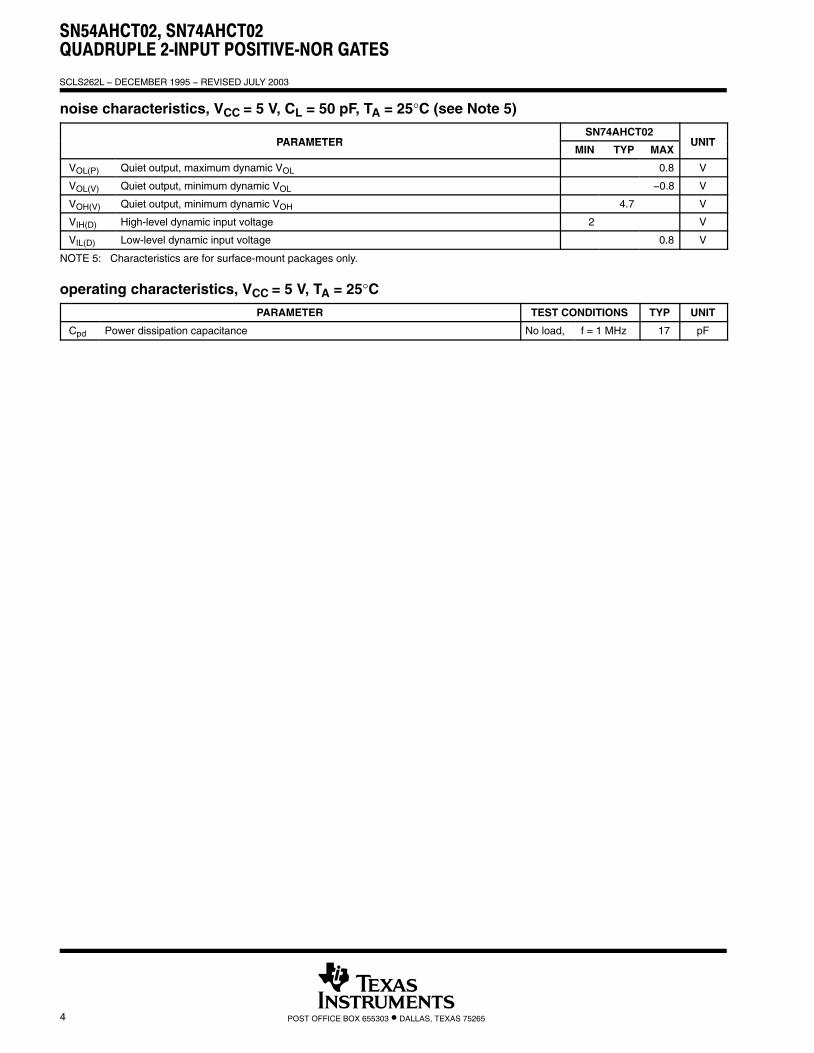
noise characteristics, VCC = 5 V, CL = 50 pF, TA = 25°C (see Note 5)
PARAMETERSN74AHCT02
UNITPARAMETERMIN TYP MAX
UNIT
VOL(P) Quiet output, maximum dynamic VOL 0.8 V
VOL(V) Quiet output, minimum dynamic VOL −0.8 V
VOH(V) Quiet output, minimum dynamic VOH 4.7 V
VIH(D) High-level dynamic input voltage 2 V
VIL(D) Low-level dynamic input voltage 0.8 V
NOTE 5: Characteristics are for surface-mount packages only.
operating characteristics, VCC = 5 V, TA = 25°CPARAMETER TEST CONDITIONS TYP UNIT
Cpd Power dissipation capacitance No load, f = 1 MHz 17 pF
SN54AHCT02, SN74AHCT02QUADRUPLE 2-INPUT POSITIVE-NOR GATES
SCLS262L − DECEMBER 1995 − REVISED JULY 2003
5POST OFFICE BOX 655303 • DALLAS, TEXAS 75265
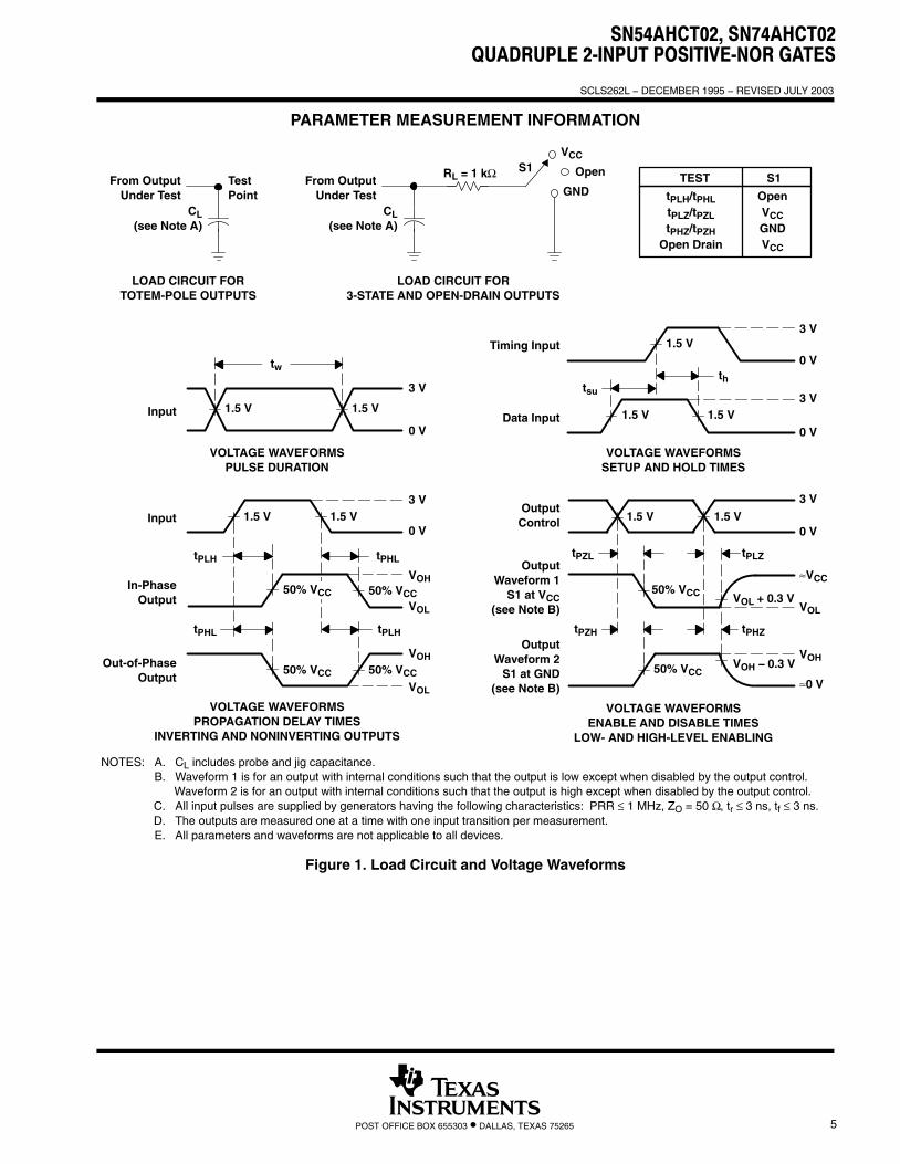
PARAMETER MEASUREMENT INFORMATION
50% VCC
3 V
3 V
0 V
0 V
thtsu
VOLTAGE WAVEFORMSSETUP AND HOLD TIMES
Data Input
tPLH
tPHL
tPHL
tPLH
VOH
VOH
VOL
VOL
3 V
0 V
50% VCC50% VCC
Input
Out-of-PhaseOutput
In-PhaseOutput
Timing Input
50% VCC
VOLTAGE WAVEFORMSPROPAGATION DELAY TIMES
INVERTING AND NONINVERTING OUTPUTS
OutputControl
OutputWaveform 1
S1 at VCC(see Note B)
OutputWaveform 2
S1 at GND(see Note B)
VOL
VOH
tPZL
tPZH
tPLZ
tPHZ
≈VCC
0 V
50% VCC VOL + 0.3 V
50% VCC≈0 V
3 V
VOLTAGE WAVEFORMSENABLE AND DISABLE TIMES
LOW- AND HIGH-LEVEL ENABLING
tPLH/tPHLtPLZ/tPZLtPHZ/tPZH
Open Drain
OpenVCCGNDVCC
TEST S1
3 V
0 V
tw
VOLTAGE WAVEFORMSPULSE DURATION
Input
NOTES: A. CL includes probe and jig capacitance.B. Waveform 1 is for an output with internal conditions such that the output is low except when disabled by the output control.
Waveform 2 is for an output with internal conditions such that the output is high except when disabled by the output control.C. All input pulses are supplied by generators having the following characteristics: PRR ≤ 1 MHz, ZO = 50 Ω, tr ≤ 3 ns, tf ≤ 3 ns.D. The outputs are measured one at a time with one input transition per measurement.E. All parameters and waveforms are not applicable to all devices.
From OutputUnder Test
CL(see Note A)
LOAD CIRCUIT FOR3-STATE AND OPEN-DRAIN OUTPUTS
S1VCC
RL = 1 kΩGND
From OutputUnder Test
CL(see Note A)
TestPoint
LOAD CIRCUIT FORTOTEM-POLE OUTPUTS
Open
VOH − 0.3 V
1.5 V 1.5 V
1.5 V
1.5 V 1.5 V
1.5 V 1.5 V1.5 V 1.5 V
Figure 1. Load Circuit and Voltage Waveforms
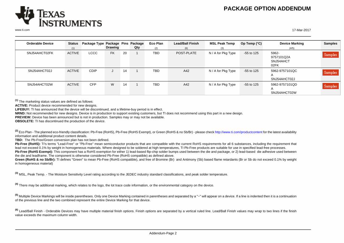
PACKAGE OPTION ADDENDUM
www.ti.com 17-Mar-2017
Addendum-Page 1
PACKAGING INFORMATION
Orderable Device Status(1)
Package Type PackageDrawing
Pins PackageQty
Eco Plan(2)
Lead/Ball Finish(6)
MSL Peak Temp(3)
Op Temp (°C) Device Marking(4/5)
Samples
5962-9757101Q2A ACTIVE LCCC FK 20 1 TBD POST-PLATE N / A for Pkg Type -55 to 125 5962-9757101Q2ASNJ54AHCT02FK
5962-9757101QCA ACTIVE CDIP J 14 1 TBD A42 N / A for Pkg Type -55 to 125 5962-9757101QCASNJ54AHCT02J
5962-9757101QDA ACTIVE CFP W 14 1 TBD A42 N / A for Pkg Type -55 to 125 5962-9757101QDASNJ54AHCT02W
SN74AHCT02D ACTIVE SOIC D 14 50 Green (RoHS& no Sb/Br)
CU NIPDAU Level-1-260C-UNLIM -40 to 85 AHCT02
SN74AHCT02DBR ACTIVE SSOP DB 14 2000 Green (RoHS& no Sb/Br)
CU NIPDAU Level-1-260C-UNLIM -40 to 85 HB02
SN74AHCT02DG4 ACTIVE SOIC D 14 50 Green (RoHS& no Sb/Br)
CU NIPDAU Level-1-260C-UNLIM -40 to 85 AHCT02
SN74AHCT02DGVR ACTIVE TVSOP DGV 14 2000 Green (RoHS& no Sb/Br)
CU NIPDAU Level-1-260C-UNLIM -40 to 85 HB02
SN74AHCT02DR ACTIVE SOIC D 14 2500 Green (RoHS& no Sb/Br)
CU NIPDAU Level-1-260C-UNLIM -40 to 85 AHCT02
SN74AHCT02N ACTIVE PDIP N 14 25 Pb-Free(RoHS)
CU NIPDAU N / A for Pkg Type -40 to 85 SN74AHCT02N
SN74AHCT02NSR ACTIVE SO NS 14 2000 Green (RoHS& no Sb/Br)
CU NIPDAU Level-1-260C-UNLIM -40 to 85 AHCT02
SN74AHCT02PW ACTIVE TSSOP PW 14 90 Green (RoHS& no Sb/Br)
CU NIPDAU Level-1-260C-UNLIM -40 to 85 HB02
SN74AHCT02PWR ACTIVE TSSOP PW 14 2000 Green (RoHS& no Sb/Br)
CU NIPDAU Level-1-260C-UNLIM -40 to 85 HB02
SN74AHCT02PWRE4 ACTIVE TSSOP PW 14 2000 Green (RoHS& no Sb/Br)
CU NIPDAU Level-1-260C-UNLIM -40 to 85 HB02
SN74AHCT02PWRG4 ACTIVE TSSOP PW 14 2000 Green (RoHS& no Sb/Br)
CU NIPDAU Level-1-260C-UNLIM -40 to 85 HB02
SN74AHCT02RGYR ACTIVE VQFN RGY 14 3000 Green (RoHS& no Sb/Br)
CU NIPDAU Level-2-260C-1 YEAR -40 to 85 HB02
PACKAGE OPTION ADDENDUM
www.ti.com 17-Mar-2017
Addendum-Page 2
Orderable Device Status(1)
Package Type PackageDrawing
Pins PackageQty
Eco Plan(2)
Lead/Ball Finish(6)
MSL Peak Temp(3)
Op Temp (°C) Device Marking(4/5)
Samples
SNJ54AHCT02FK ACTIVE LCCC FK 20 1 TBD POST-PLATE N / A for Pkg Type -55 to 125 5962-9757101Q2ASNJ54AHCT02FK
SNJ54AHCT02J ACTIVE CDIP J 14 1 TBD A42 N / A for Pkg Type -55 to 125 5962-9757101QCASNJ54AHCT02J
SNJ54AHCT02W ACTIVE CFP W 14 1 TBD A42 N / A for Pkg Type -55 to 125 5962-9757101QDASNJ54AHCT02W
(1) The marketing status values are defined as follows:ACTIVE: Product device recommended for new designs.LIFEBUY: TI has announced that the device will be discontinued, and a lifetime-buy period is in effect.NRND: Not recommended for new designs. Device is in production to support existing customers, but TI does not recommend using this part in a new design.PREVIEW: Device has been announced but is not in production. Samples may or may not be available.OBSOLETE: TI has discontinued the production of the device.
(2) Eco Plan - The planned eco-friendly classification: Pb-Free (RoHS), Pb-Free (RoHS Exempt), or Green (RoHS & no Sb/Br) - please check http://www.ti.com/productcontent for the latest availabilityinformation and additional product content details.TBD: The Pb-Free/Green conversion plan has not been defined.Pb-Free (RoHS): TI's terms "Lead-Free" or "Pb-Free" mean semiconductor products that are compatible with the current RoHS requirements for all 6 substances, including the requirement thatlead not exceed 0.1% by weight in homogeneous materials. Where designed to be soldered at high temperatures, TI Pb-Free products are suitable for use in specified lead-free processes.Pb-Free (RoHS Exempt): This component has a RoHS exemption for either 1) lead-based flip-chip solder bumps used between the die and package, or 2) lead-based die adhesive used betweenthe die and leadframe. The component is otherwise considered Pb-Free (RoHS compatible) as defined above.Green (RoHS & no Sb/Br): TI defines "Green" to mean Pb-Free (RoHS compatible), and free of Bromine (Br) and Antimony (Sb) based flame retardants (Br or Sb do not exceed 0.1% by weightin homogeneous material)
(3) MSL, Peak Temp. - The Moisture Sensitivity Level rating according to the JEDEC industry standard classifications, and peak solder temperature.
(4) There may be additional marking, which relates to the logo, the lot trace code information, or the environmental category on the device.
(5) Multiple Device Markings will be inside parentheses. Only one Device Marking contained in parentheses and separated by a "~" will appear on a device. If a line is indented then it is a continuationof the previous line and the two combined represent the entire Device Marking for that device.
(6) Lead/Ball Finish - Orderable Devices may have multiple material finish options. Finish options are separated by a vertical ruled line. Lead/Ball Finish values may wrap to two lines if the finishvalue exceeds the maximum column width.

PACKAGE OPTION ADDENDUM
www.ti.com 17-Mar-2017
Addendum-Page 3
Important Information and Disclaimer:The information provided on this page represents TI's knowledge and belief as of the date that it is provided. TI bases its knowledge and belief on informationprovided by third parties, and makes no representation or warranty as to the accuracy of such information. Efforts are underway to better integrate information from third parties. TI has taken andcontinues to take reasonable steps to provide representative and accurate information but may not have conducted destructive testing or chemical analysis on incoming materials and chemicals.TI and TI suppliers consider certain information to be proprietary, and thus CAS numbers and other limited information may not be available for release.
In no event shall TI's liability arising out of such information exceed the total purchase price of the TI part(s) at issue in this document sold by TI to Customer on an annual basis.
OTHER QUALIFIED VERSIONS OF SN54AHCT02, SN74AHCT02 :
• Catalog: SN74AHCT02
• Military: SN54AHCT02
NOTE: Qualified Version Definitions:
• Catalog - TI's standard catalog product
• Military - QML certified for Military and Defense Applications
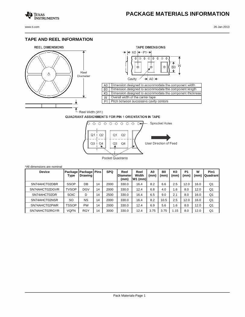
TAPE AND REEL INFORMATION
*All dimensions are nominal
Device PackageType
PackageDrawing
Pins SPQ ReelDiameter
(mm)
ReelWidth
W1 (mm)
A0(mm)
B0(mm)
K0(mm)
P1(mm)
W(mm)
Pin1Quadrant
SN74AHCT02DBR SSOP DB 14 2000 330.0 16.4 8.2 6.6 2.5 12.0 16.0 Q1
SN74AHCT02DGVR TVSOP DGV 14 2000 330.0 12.4 6.8 4.0 1.6 8.0 12.0 Q1
SN74AHCT02DR SOIC D 14 2500 330.0 16.4 6.5 9.0 2.1 8.0 16.0 Q1
SN74AHCT02NSR SO NS 14 2000 330.0 16.4 8.2 10.5 2.5 12.0 16.0 Q1
SN74AHCT02PWR TSSOP PW 14 2000 330.0 12.4 6.9 5.6 1.6 8.0 12.0 Q1
SN74AHCT02RGYR VQFN RGY 14 3000 330.0 12.4 3.75 3.75 1.15 8.0 12.0 Q1
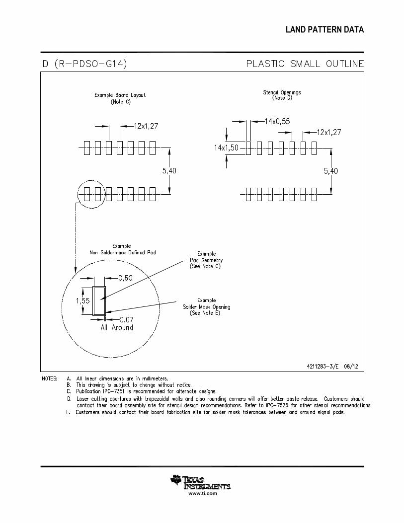
PACKAGE MATERIALS INFORMATION
www.ti.com 26-Jan-2013
Pack Materials-Page 1

*All dimensions are nominal
Device Package Type Package Drawing Pins SPQ Length (mm) Width (mm) Height (mm)
SN74AHCT02DBR SSOP DB 14 2000 367.0 367.0 38.0
SN74AHCT02DGVR TVSOP DGV 14 2000 367.0 367.0 35.0
SN74AHCT02DR SOIC D 14 2500 367.0 367.0 38.0
SN74AHCT02NSR SO NS 14 2000 367.0 367.0 38.0
SN74AHCT02PWR TSSOP PW 14 2000 367.0 367.0 35.0
SN74AHCT02RGYR VQFN RGY 14 3000 367.0 367.0 35.0
PACKAGE MATERIALS INFORMATION
www.ti.com 26-Jan-2013
Pack Materials-Page 2
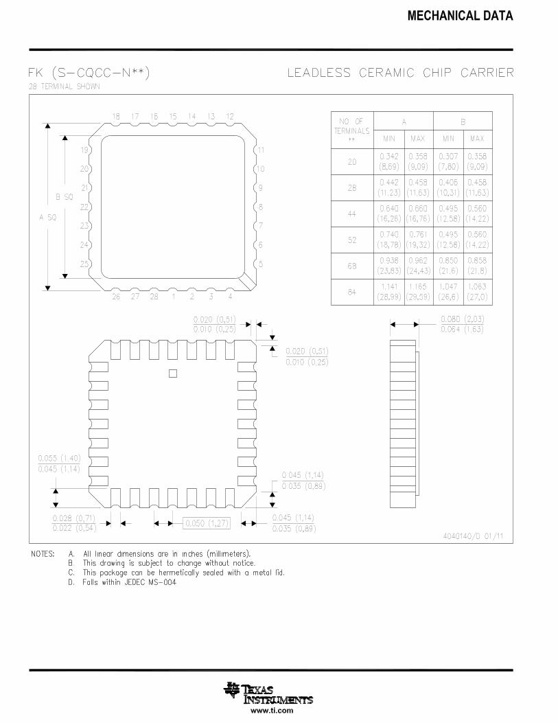
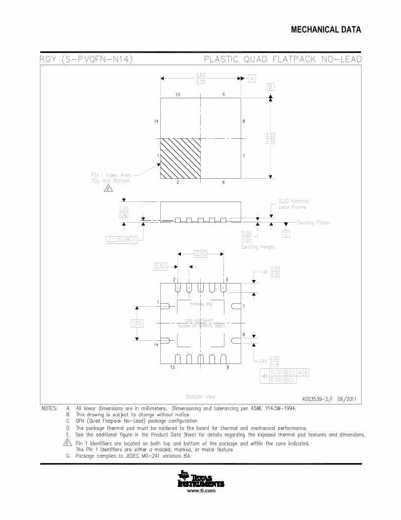

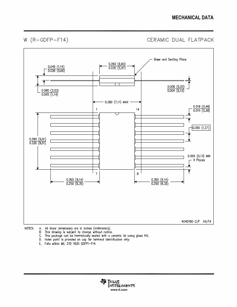
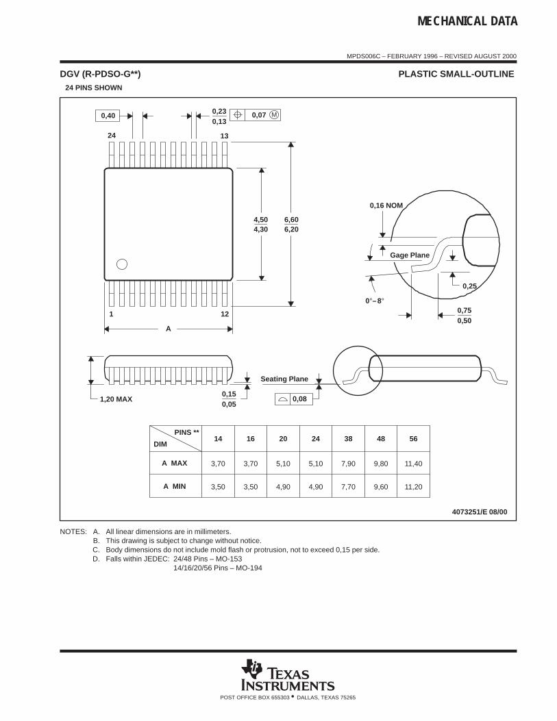
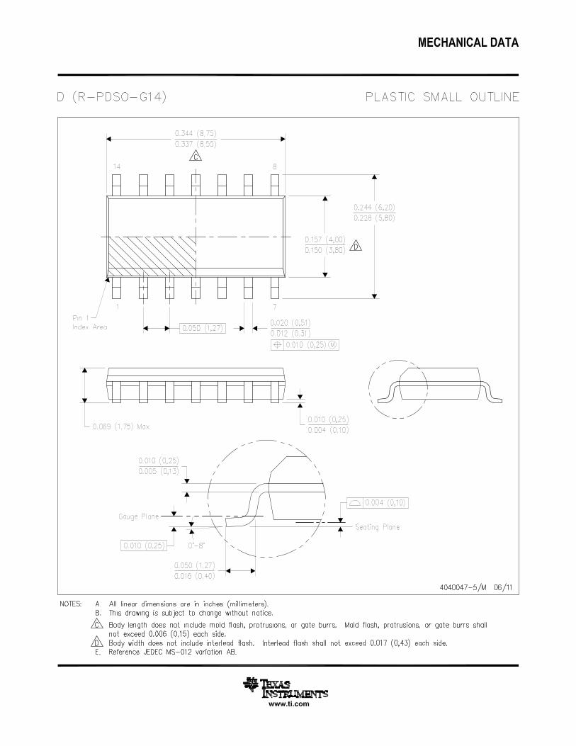
MECHANICAL DATA
MPDS006C – FEBRUARY 1996 – REVISED AUGUST 2000
POST OFFICE BOX 655303 • DALLAS, TEXAS 75265
DGV (R-PDSO-G**) PLASTIC SMALL-OUTLINE 24 PINS SHOWN
14
3,70
3,50 4,90
5,10
20DIM
PINS **
4073251/E 08/00
1,20 MAX
Seating Plane
0,050,15
0,25
0,500,75
0,230,13
1 12
24 13
4,304,50
0,16 NOM
Gage Plane
A
7,90
7,70
382416
4,90
5,103,70
3,50
A MAX
A MIN
6,606,20
11,20
11,40
56
9,60
9,80
48
0,08
M0,070,40
0°–�8°
NOTES: A. All linear dimensions are in millimeters.B. This drawing is subject to change without notice.C. Body dimensions do not include mold flash or protrusion, not to exceed 0,15 per side.D. Falls within JEDEC: 24/48 Pins – MO-153
14/16/20/56 Pins – MO-194
www.ti.com
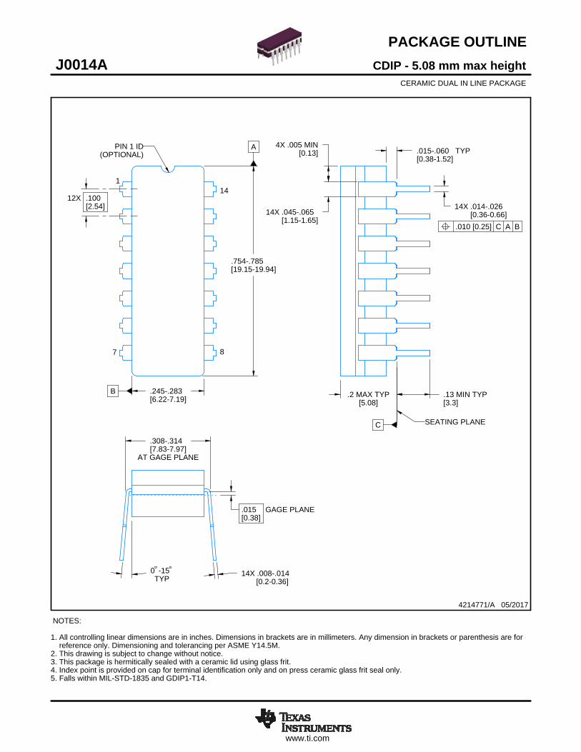
PACKAGE OUTLINE
C
14X .008-.014 [0.2-0.36]TYP
-150
AT GAGE PLANE
-.314.308-7.977.83[ ]
14X -.026.014-0.660.36[ ]14X -.065.045
-1.651.15[ ]
.2 MAX TYP[5.08]
.13 MIN TYP[3.3]
TYP-.060.015-1.520.38[ ]
4X .005 MIN[0.13]
12X .100[2.54]
.015 GAGE PLANE[0.38]
A
-.785.754-19.9419.15[ ]
B -.283.245-7.196.22[ ]
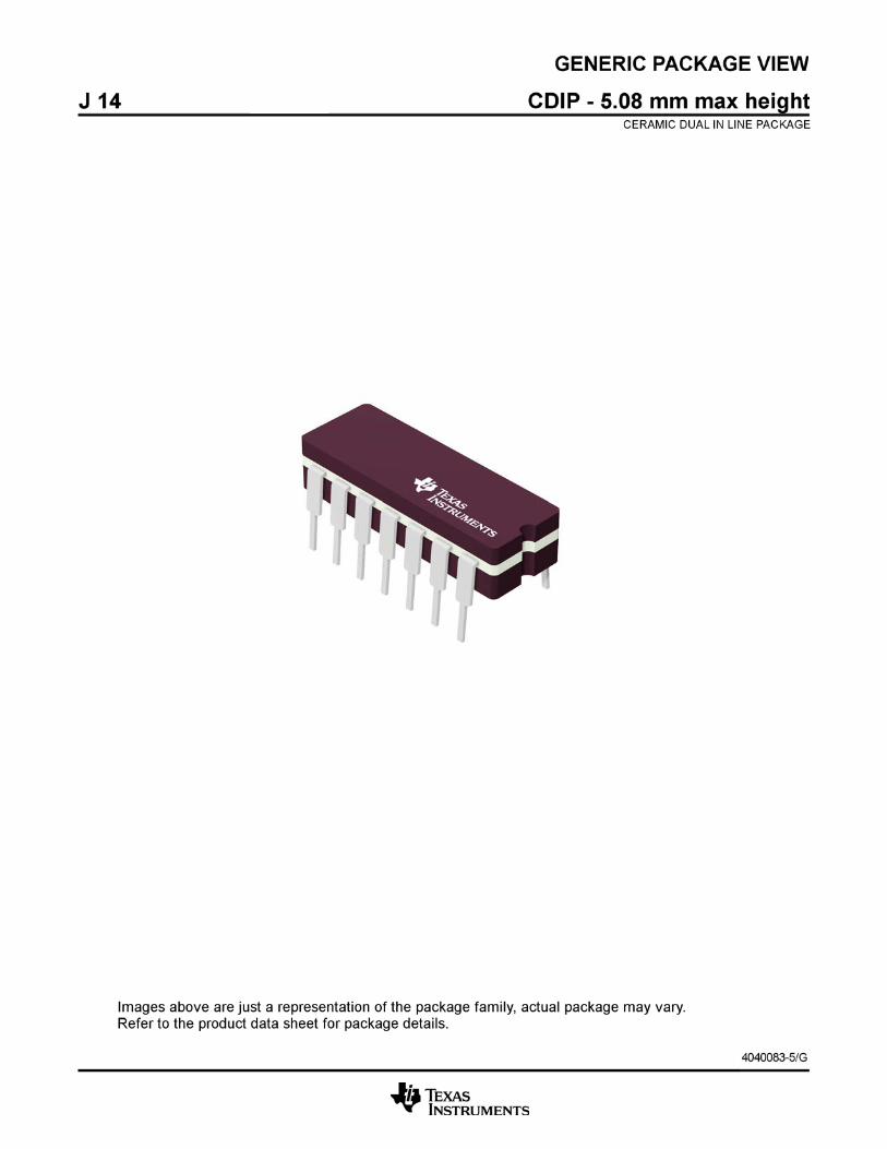
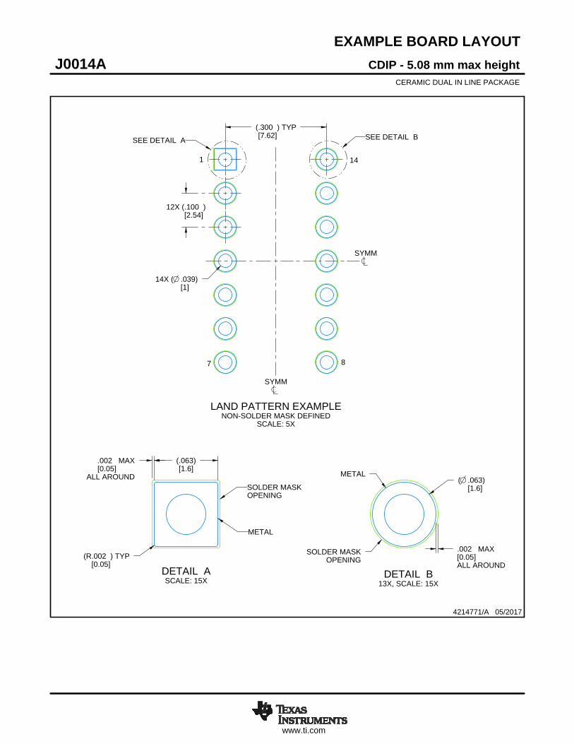
CDIP - 5.08 mm max heightJ0014ACERAMIC DUAL IN LINE PACKAGE
4214771/A 05/2017
NOTES: 1. All controlling linear dimensions are in inches. Dimensions in brackets are in millimeters. Any dimension in brackets or parenthesis are for reference only. Dimensioning and tolerancing per ASME Y14.5M.2. This drawing is subject to change without notice. 3. This package is hermitically sealed with a ceramic lid using glass frit.4. Index point is provided on cap for terminal identification only and on press ceramic glass frit seal only.5. Falls within MIL-STD-1835 and GDIP1-T14.
7 8
141
PIN 1 ID(OPTIONAL)
SCALE 0.900
SEATING PLANE
.010 [0.25] C A B
www.ti.com
EXAMPLE BOARD LAYOUT
ALL AROUND[0.05]
MAX.002
.002 MAX[0.05]ALL AROUND
SOLDER MASKOPENING
METAL
(.063)[1.6]
(R.002 ) TYP[0.05]
14X ( .039)[1]
( .063)[1.6]
12X (.100 )[2.54]
(.300 ) TYP[7.62]
CDIP - 5.08 mm max heightJ0014ACERAMIC DUAL IN LINE PACKAGE
4214771/A 05/2017
LAND PATTERN EXAMPLENON-SOLDER MASK DEFINED
SCALE: 5X
SEE DETAIL A SEE DETAIL B
SYMM
SYMM
1
7 8
14
DETAIL ASCALE: 15X
SOLDER MASKOPENING
METAL
DETAIL B13X, SCALE: 15X
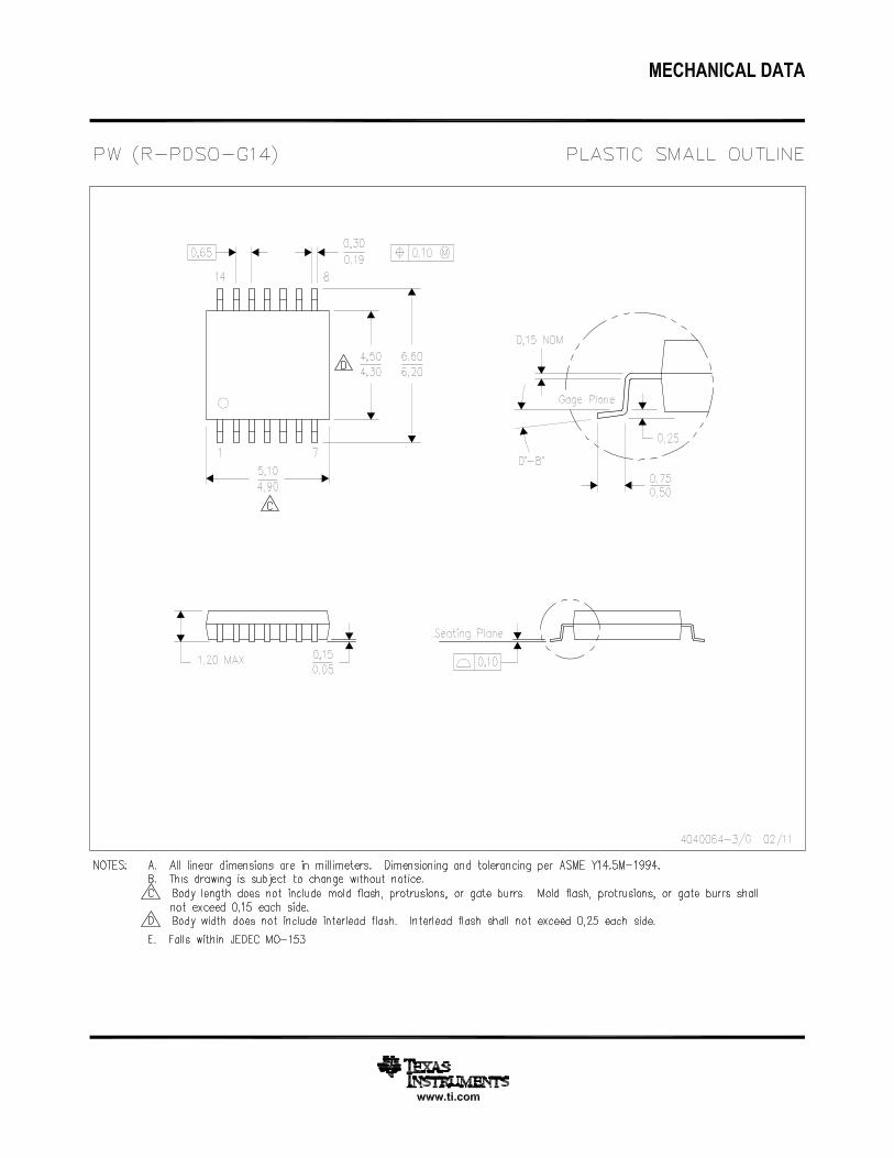

MECHANICAL DATA
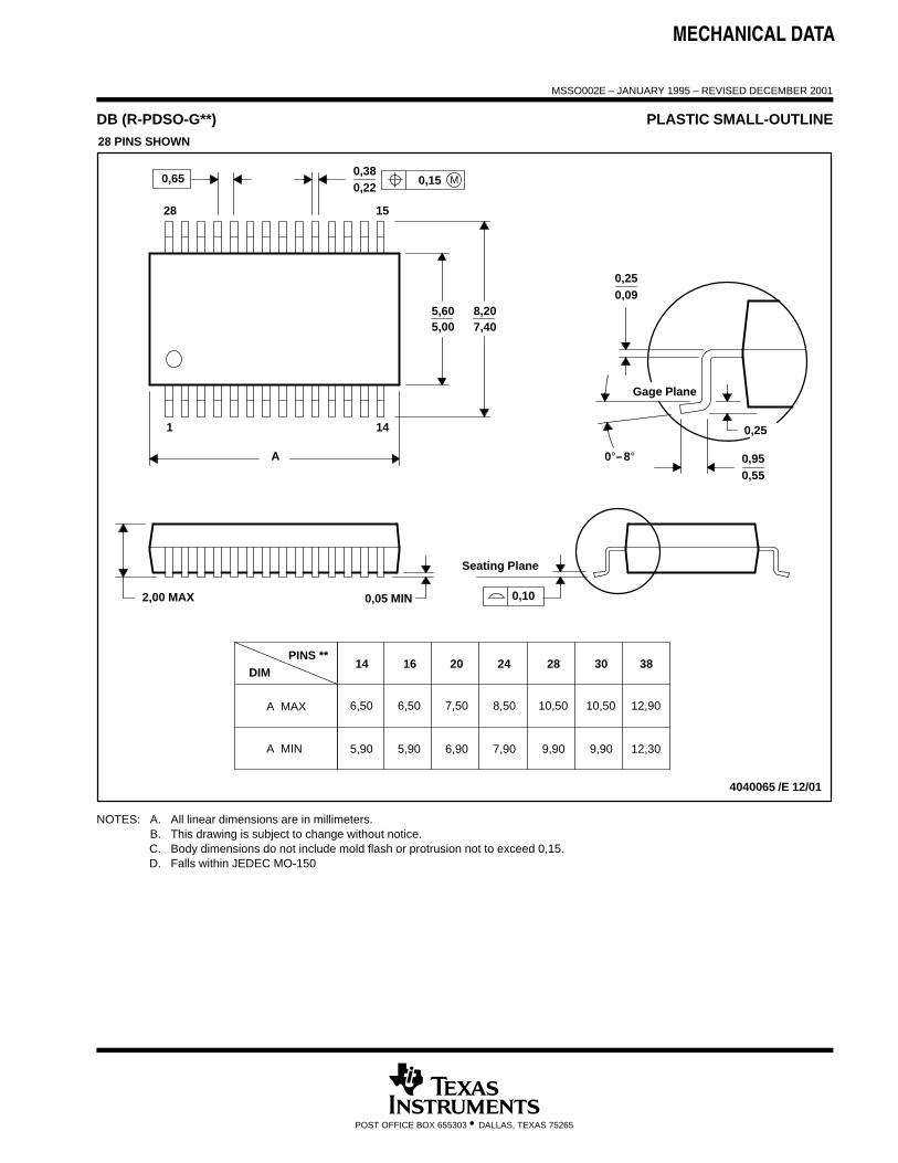
MSSO002E – JANUARY 1995 – REVISED DECEMBER 2001
POST OFFICE BOX 655303 • DALLAS, TEXAS 75265
DB (R-PDSO-G**) PLASTIC SMALL-OUTLINE
4040065 /E 12/01
28 PINS SHOWN
Gage Plane
8,207,40
0,550,95
0,25
38
12,90
12,30
28
10,50
24
8,50
Seating Plane
9,907,90
30
10,50
9,90
0,38
5,605,00
15
0,22
14
A
28
1
2016
6,506,50
14
0,05 MIN
5,905,90
DIM
A MAX
A MIN
PINS **
2,00 MAX
6,90
7,50
0,65 M0,15
0°–�8°
0,10
0,090,25
NOTES: A. All linear dimensions are in millimeters.B. This drawing is subject to change without notice.C. Body dimensions do not include mold flash or protrusion not to exceed 0,15.D. Falls within JEDEC MO-150
IMPORTANT NOTICE
Texas Instruments Incorporated (TI) reserves the right to make corrections, enhancements, improvements and other changes to itssemiconductor products and services per JESD46, latest issue, and to discontinue any product or service per JESD48, latest issue. Buyersshould obtain the latest relevant information before placing orders and should verify that such information is current and complete.TI’s published terms of sale for semiconductor products (http://www.ti.com/sc/docs/stdterms.htm) apply to the sale of packaged integratedcircuit products that TI has qualified and released to market. Additional terms may apply to the use or sale of other types of TI products andservices.Reproduction of significant portions of TI information in TI data sheets is permissible only if reproduction is without alteration and isaccompanied by all associated warranties, conditions, limitations, and notices. TI is not responsible or liable for such reproduceddocumentation. Information of third parties may be subject to additional restrictions. Resale of TI products or services with statementsdifferent from or beyond the parameters stated by TI for that product or service voids all express and any implied warranties for theassociated TI product or service and is an unfair and deceptive business practice. TI is not responsible or liable for any such statements.Buyers and others who are developing systems that incorporate TI products (collectively, “Designers”) understand and agree that Designersremain responsible for using their independent analysis, evaluation and judgment in designing their applications and that Designers havefull and exclusive responsibility to assure the safety of Designers' applications and compliance of their applications (and of all TI productsused in or for Designers’ applications) with all applicable regulations, laws and other applicable requirements. Designer represents that, withrespect to their applications, Designer has all the necessary expertise to create and implement safeguards that (1) anticipate dangerousconsequences of failures, (2) monitor failures and their consequences, and (3) lessen the likelihood of failures that might cause harm andtake appropriate actions. Designer agrees that prior to using or distributing any applications that include TI products, Designer willthoroughly test such applications and the functionality of such TI products as used in such applications.TI’s provision of technical, application or other design advice, quality characterization, reliability data or other services or information,including, but not limited to, reference designs and materials relating to evaluation modules, (collectively, “TI Resources”) are intended toassist designers who are developing applications that incorporate TI products; by downloading, accessing or using TI Resources in anyway, Designer (individually or, if Designer is acting on behalf of a company, Designer’s company) agrees to use any particular TI Resourcesolely for this purpose and subject to the terms of this Notice.TI’s provision of TI Resources does not expand or otherwise alter TI’s applicable published warranties or warranty disclaimers for TIproducts, and no additional obligations or liabilities arise from TI providing such TI Resources. TI reserves the right to make corrections,enhancements, improvements and other changes to its TI Resources. TI has not conducted any testing other than that specificallydescribed in the published documentation for a particular TI Resource.Designer is authorized to use, copy and modify any individual TI Resource only in connection with the development of applications thatinclude the TI product(s) identified in such TI Resource. NO OTHER LICENSE, EXPRESS OR IMPLIED, BY ESTOPPEL OR OTHERWISETO ANY OTHER TI INTELLECTUAL PROPERTY RIGHT, AND NO LICENSE TO ANY TECHNOLOGY OR INTELLECTUAL PROPERTYRIGHT OF TI OR ANY THIRD PARTY IS GRANTED HEREIN, including but not limited to any patent right, copyright, mask work right, orother intellectual property right relating to any combination, machine, or process in which TI products or services are used. Informationregarding or referencing third-party products or services does not constitute a license to use such products or services, or a warranty orendorsement thereof. Use of TI Resources may require a license from a third party under the patents or other intellectual property of thethird party, or a license from TI under the patents or other intellectual property of TI.TI RESOURCES ARE PROVIDED “AS IS” AND WITH ALL FAULTS. TI DISCLAIMS ALL OTHER WARRANTIES ORREPRESENTATIONS, EXPRESS OR IMPLIED, REGARDING RESOURCES OR USE THEREOF, INCLUDING BUT NOT LIMITED TOACCURACY OR COMPLETENESS, TITLE, ANY EPIDEMIC FAILURE WARRANTY AND ANY IMPLIED WARRANTIES OFMERCHANTABILITY, FITNESS FOR A PARTICULAR PURPOSE, AND NON-INFRINGEMENT OF ANY THIRD PARTY INTELLECTUALPROPERTY RIGHTS. TI SHALL NOT BE LIABLE FOR AND SHALL NOT DEFEND OR INDEMNIFY DESIGNER AGAINST ANY CLAIM,INCLUDING BUT NOT LIMITED TO ANY INFRINGEMENT CLAIM THAT RELATES TO OR IS BASED ON ANY COMBINATION OFPRODUCTS EVEN IF DESCRIBED IN TI RESOURCES OR OTHERWISE. IN NO EVENT SHALL TI BE LIABLE FOR ANY ACTUAL,DIRECT, SPECIAL, COLLATERAL, INDIRECT, PUNITIVE, INCIDENTAL, CONSEQUENTIAL OR EXEMPLARY DAMAGES INCONNECTION WITH OR ARISING OUT OF TI RESOURCES OR USE THEREOF, AND REGARDLESS OF WHETHER TI HAS BEENADVISED OF THE POSSIBILITY OF SUCH DAMAGES.Unless TI has explicitly designated an individual product as meeting the requirements of a particular industry standard (e.g., ISO/TS 16949and ISO 26262), TI is not responsible for any failure to meet such industry standard requirements.Where TI specifically promotes products as facilitating functional safety or as compliant with industry functional safety standards, suchproducts are intended to help enable customers to design and create their own applications that meet applicable functional safety standardsand requirements. Using products in an application does not by itself establish any safety features in the application. Designers mustensure compliance with safety-related requirements and standards applicable to their applications. Designer may not use any TI products inlife-critical medical equipment unless authorized officers of the parties have executed a special contract specifically governing such use.Life-critical medical equipment is medical equipment where failure of such equipment would cause serious bodily injury or death (e.g., lifesupport, pacemakers, defibrillators, heart pumps, neurostimulators, and implantables). Such equipment includes, without limitation, allmedical devices identified by the U.S. Food and Drug Administration as Class III devices and equivalent classifications outside the U.S.TI may expressly designate certain products as completing a particular qualification (e.g., Q100, Military Grade, or Enhanced Product).Designers agree that it has the necessary expertise to select the product with the appropriate qualification designation for their applicationsand that proper product selection is at Designers’ own risk. Designers are solely responsible for compliance with all legal and regulatoryrequirements in connection with such selection.Designer will fully indemnify TI and its representatives against any damages, costs, losses, and/or liabilities arising out of Designer’s non-compliance with the terms and provisions of this Notice.
Mailing Address: Texas Instruments, Post Office Box 655303, Dallas, Texas 75265Copyright © 2017, Texas Instruments Incorporated