Embed Size (px)
Citation preview

RT5112®
DS5112-02 January 2019 www.richtek.com1
Copyright 2019 Richtek Technology Corporation. All rights reserved. is a registered trademark of Richtek Technology Corporation.©
General Description
The RT5112 device is a smart power management IC
which includes a low-quiescent-current HCOT Buck
converter, a ACOT Boost converter and four high PSRR
low dropout regulators (LDO). One can control the channel
power sequence, output voltage level and DVS slew rate
by setting registers via I2C interface. The output voltage
OVP/UVP, OCP and OTP protection are built in the
RT5112. The RT5112 is available in a WL-CSP-25B
2.2x2.3 (BSC) package.
Smart Power-Management Integrated Circuit for CameraModule Application
Features
System Control
Hardware Enable Pin
I2C Controlled Interface
Programmable Channel Power Sequence
IRQ Output for Indication
Over-Voltage Protection
Under-Voltage Protection
Over-Current Protection
Over-Temperature Protection
Available in a WL-CSP-25B 2.2x2.3 (BSC) Package
High Efficiency Buck Converter
Wide 2.5V to 5.5V Operating Input Range
Programmable Output Voltage from 0.6V to 3.3V
with 12.5mV/Step
Maximum Continuous Load Current : 1.2A
HCOT Control Operation
Low Quiescent Current
Flexible Boost Converter
Wide 2.5V to 4.4V Operating Input Range
Programmable Output Voltage from 4.5 V to 5.5V
with 25mV/Step
Maximum Continuous Load Current : 1A
ACOT Control Operation
Low Quiescent Current
Four Low Dropout Regulators
Wide 1.9V to 5.5V Operating Input Range
Programmable Output Voltage from 0.6V to 3.775V
with 25mV/Step
High PSRR : 70dB @ 1kHz, 40dB @ 100kHz with
LDO1 / LDO2
High PSRR : 50dB @ 1kHz, 40dB @ 10kHz with LDO3
/ LDO4
300mA Low Dropout Voltage Regulators
Low Quiescent Current
Ordering Information
Applications Camera Module
Optical Module
SSD
Marking Information
Package TypeWSC : WL-CSP-25B 2.2x2.3 (BSC)
RT5112
Note :
Richtek products are :
RoHS compliant and compatible with the current require-
ments of IPC/JEDEC J-STD-020.
Suitable for use in SnPb or Pb-free soldering processes.
1D YMDNN
1D : Product Code
YMDNN : Date Code

RT5112
2
DS5112-02 January 2019www.richtek.com
©Copyright 2019 Richtek Technology Corporation. All rights reserved. is a registered trademark of Richtek Technology Corporation.
Pin Configuration(TOP VIEW)
WL-CSP-25B 2.2 x 2.3 (BSC)
Typical Application Circuit
LXBSTBSTVOUTLXB VINB
GNDB GNDBST
FB1 BSTEN
HWENNC DGND SCL
VIN4 VIN3 VIN12VSYS
LDO4 LDO3 LDO1AGND
LXBST
INTRB
SDA
REF
LDO2
E1
A1
B1
C1
D1
E2
A2
B2
C2
D2
E3
A3
B3
C3
D3
E4
A4
B4
C4
D4
E5
A5
B5
C5
D5
Driver&
Control
1.2A Buck
Control Logic
I2C
Ref
300mA LDO1Driver &Control
300mA LDO2Driver &Control
300mA LDO3Driver &Control
300mA LDO4Driver &Control
VOUT_BUCK0.6V to 3.3V
FB1
GNDB
VIN_BST3.8V
GNDBST
HWEN
BSTEN
SCL
SDA
Driver&
Control
1A Boost
DGND
VOUT_LDO10.6 to 3.775V
LDO2
VIN_B3.8V
VSYS
INTRB
I2C
BUS
REF
BSTVOUT
VIN3
VIN4
C110µF
L11µH
C210µF
C131µF
C1110nF
L20.47µH
C310µF
C422µF
C62.2µF
C52.2µF
C72.2µF
C92.2µF
C82.2µF
C122.2µF
C102.2µF
VINB
LXBST
LDO1
VIN12
LDO3
LDO4
LXB
RT5112
VOUT_LDO20.6 to 3.775V
VOUT_LDO30.6 to 3.775V
VOUT_LDO40.6 to 3.775V
VIN_B3.8V
VIN_VIN123.8V
VIN_VIN33.8V
VIN_VIN43.8V
R1
2.2K
VOUT_BST4.5V to 5.5V
A4, A5
A3
B5
C2
B3
E5
D5
E4
E2
D2
D1
E1
C3
D4
C5
C4
B4
D3
B1
B2
A1
A2
VIN_SYS3.8V
AGND
E3

RT5112
3
DS5112-02 January 2019 www.richtek.com
©Copyright 2019 Richtek Technology Corporation. All rights reserved. is a registered trademark of Richtek Technology Corporation.
Component List of Evaluation Board
Reference Qty Part Number Description Package Manufacturer
C1, C2, C3 1 JMK105CBJ106MV-F 10F/X5R/6.3V 0402 TAIYO YUDEN
C4 1 JMK107BBJ226MA-T 22F/X5R/6.3V 0603 TAIYO YUDEN
C5, C8, C12 1 JMK105BJ225KV-F 2.2F/X5R/6.3V 0402 TAIYO YUDEN
C6, C7, C9, C10 1 GRM033R60J225ME47D 2.2F/X5R/6.3V 0201 MURATA
C11 1 LMK105BJ103KV-F 10nF/X5R/6.3V 0402 TAIYO YUDEN
C13 1 LMK063BBJ105MPLF 1F/X5R/10V 0201 TAIYO YUDEN
L1 1 MEKK2016T1R0M 1H/3.1A/50m 2016 TAIYO YUDEN
L2 1 DFE201210S-R47MH=P2 0.47H/3.4A/32m 2012 MURATA
Functional Pin DescriptionPin No. Pin Name Pin Function
A1 LXB Buck switch output. Connect this pin to an inductor with a wide PCB trace.
A2 VINB Supply voltage input of Buck. The IC operates from a 2.5V to 5.5V input rail. It requires a 10F decouple ceramic capacitor. Connect this pin to input voltage with a wide PCB trace.
A3 BSTVOUT
Boost output pin. PCB trace length from BSTVOUT to the output filter capacitor should be as short and wide as possible. It requires a 22F decouple ceramic capacitor. BSTVOUT is completely disconnected from LXBST when Boost is at off state.
A4, A5 LXBST Boost switch output. Connect this pin to an inductor with a wide PCB trace and keep the PCB trace length as short and wide as possible to reduce EMI and voltage spike.
B1 GNDB Buck power ground.
B2 FB1 Feedback of Buck. Directly connect the Buck’s output to this pin.
B3 BSTEN Boost enable control input.
B4 INTRB Interrupt output. Open drain output. When interrupt happens, interrupt pin is pulled down.
B5 GNDBST Boost power ground.
C1 NC NC internal connection and should keep floating state.
C2 HWEN Chip enable control input.
C3 DGND Digital ground.
C4 SDA I2C data pin.
C5 SCL I2C clock signal input.
D1 VIN4 LDO4 power supply input. It requires a 2.2F decouple ceramic capacitor.
D2 VIN3 LDO3 power supply input. It requires a 2.2F decouple ceramic capacitor.
D3 VSYS System analog power supply. It requires a 1F decouple ceramic capacitor. It also connected to VINB externally.

RT5112
4
DS5112-02 January 2019www.richtek.com
©Copyright 2019 Richtek Technology Corporation. All rights reserved. is a registered trademark of Richtek Technology Corporation.
Pin No. Pin Name Pin Function
D4 REF Internal reference output. It requires a 10nF decouple ceramic capacitor.
D5 VIN12 LDO1 and 2 power supply input. It requires a 2.2F decouple ceramic capacitor.
E1 LDO4 LDO4 output. It requires a 2.2F decouple ceramic capacitor.
E2 LDO3 LDO3 output. It requires a 2.2F decouple ceramic capacitor.
E3 AGND Analog ground.
E4 LDO2 LDO2 output. It requires a 2.2F decouple ceramic capacitor.
E5 LDO1 LDO1 output. It requires a 2.2F decouple ceramic capacitor.
Functional Block Diagram
Driver&
Control
1.2A Buck
Control Logic
I2C
Ref
300mA LDO1Driver &Control
300mA LDO2Driver &Control
300mA LDO3Driver &Control
300mA LDO4Driver &Control
LXB
FB1
GNDB
LXBST
GNDBST
HWEN
BSTEN
SCL
SDA
Driver&
Control
1A Boost
AGNDDGND
LDO1
LDO2
LDO3
LDO4
VINB
VSYS
INTRB
REF
BSTVOUT
VIN12
VIN3
VIN4
RT5112
5
DS5112-02 January 2019 www.richtek.com
©Copyright 2019 Richtek Technology Corporation. All rights reserved. is a registered trademark of Richtek Technology Corporation.
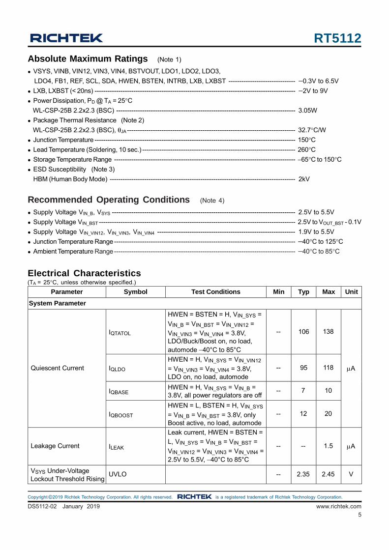
Electrical Characteristics
Parameter Symbol Test Conditions Min Typ Max Unit
System Parameter
Quiescent Current
IQTATOL
HWEN = BSTEN = H, VIN_SYS =
VIN_B = VIN_BST = VIN_VIN12 =
VIN_VIN3 = VIN_VIN4 = 3.8V, LDO/Buck/Boost on, no load, automode 40°C to 85°C
-- 106 138
A IQLDO HWEN = H, VIN_SYS = VIN_VIN12
= VIN_VIN3 = VIN_VIN4 = 3.8V, LDO on, no load, automode
-- 95 118
IQBASE HWEN = H, VIN_SYS = VIN_B = 3.8V, all power regulators are off
-- 7 10
IQBOOST HWEN = L, BSTEN = H, VIN_SYS
= VIN_B = VIN_BST = 3.8V, only Boost active, no load, automode
-- 12 20
Leakage Current ILEAK
Leak current, HWEN = BSTEN =
L, VIN_SYS = VIN_B = VIN_BST =
VIN_VIN12 = VIN_VIN3 = VIN_VIN4 = 2.5V to 5.5V, 40°C to 85°C
-- -- 1.5 A
VSYS Under-Voltage Lockout Threshold Rising
UVLO -- 2.35 2.45 V
(TA = 25°C, unless otherwise specified.)
Recommended Operating Conditions (Note 4)
Supply Voltage VIN_B, VSYS ------------------------------------------------------------------------------------- 2.5V to 5.5V
Supply Voltage VIN_BST ------------------------------------------------------------------------------------------- 2.5V to VOUT_BST - 0.1V
Supply Voltage VIN_VIN12, VIN_VIN3, VIN_VIN4 ---------------------------------------------------------------- 1.9V to 5.5V
Junction Temperature Range------------------------------------------------------------------------------------ −40°C to 125°C Ambient Temperature Range------------------------------------------------------------------------------------ −40°C to 85°C
Absolute Maximum Ratings (Note 1)
VSYS, VINB, VIN12, VIN3, VIN4, BSTVOUT, LDO1, LDO2, LDO3,
LDO4, FB1, REF, SCL, SDA, HWEN, BSTEN, INTRB, LXB, LXBST ------------------------------- −0.3V to 6.5V
LXB, LXBST (< 20ns) --------------------------------------------------------------------------------------------- −2V to 9V
Power Dissipation, PD @ TA = 25°C
WL-CSP-25B 2.2x2.3 (BSC) ----------------------------------------------------------------------------------- 3.05W
Package Thermal Resistance (Note 2)
WL-CSP-25B 2.2x2.3 (BSC), θJA------------------------------------------------------------------------------ 32.7°C/W
Junction Temperature --------------------------------------------------------------------------------------------- 150°C Lead Temperature (Soldering, 10 sec.) ----------------------------------------------------------------------- 260°C Storage Temperature Range ------------------------------------------------------------------------------------ −65°C to 150°C ESD Susceptibility (Note 3)
HBM (Human Body Mode) -------------------------------------------------------------------------------------- 2kV

RT5112
6
DS5112-02 January 2019www.richtek.com
©Copyright 2019 Richtek Technology Corporation. All rights reserved. is a registered trademark of Richtek Technology Corporation.
Parameter Symbol Test Conditions Min Typ Max Unit
Hysteresis Voltage of UVLO
UVLO_H -- 100 -- mV
HWEN and BSTEN Control
HWEN and BSTEN Low Level Input Voltage VIL -- -- 0.4 V
HWEN and BSTEN High Level Input Voltage VIH 1.2 -- -- V
HWEN and BSTEN Pull Down Resistor REN -- 1 - M
Step Down Buck Converter (VIN_B = 3.8V, C1 = C2 = 10F, L1 = 1H)
Input Voltage Range VIN_B 2.5 -- 5.5 V
Output Voltage Range VOUT_BUCK
0.6 -- 3.3 V
Output Voltage Step -- 12.5 -- mV
Output Voltage Accuracy VOUT_ACC_BUCK All output range of VOUT_BUCK,
IOUT = IOUT(MAX) 2 -- 2 %
Switching Frequency fSW_BUCK VOUT_BUCK = 1.1V, operating under CCM
2 2.5 3 MHz
P-Channel MOSFET On Resistance RON_HG_BUCK From VINB pin to LXB pin -- 150 200 m
N-Channel MOSFET On Resistance RON_LG_BUCK From LXB pin to GNDB pin -- 70 140 m
Maximum Duty Cycle DMAX_BUCK -- -- 100 %
Output Discharge Resistor RDIS_BUCK 80 100 140
Over-Voltage Rising Threshold Detection OVP_R_BUCK --
VOUT_
BUCK x 120%
-- V
Over-Voltage Falling Threshold Detection OVP_F_BUCK --
VOUT_
BUCK x 109%
-- V
Under-Voltage Rising Threshold Detection UVP_R_BUCK --
VOUT_
BUCK x 92%
-- V
Under-Voltage Falling Threshold Detection UVP_F_BUCK --
VOUT_
BUCK x 80%
-- V
FB1 Leakage Current IFB_LK
Buck disable, 0x0B[7] = 0 (Buck
discharge disable), VIN_B = 5.5V,
VLXB = 5.5V, VFB1 = 5.5V
0 50 100 nA
Switch Leakage Current ILXB_LK
Buck disable, 0x0B[7] = 0 (Buck
discharge disable), VIN_B = 5.5V,
VLXB = 0 or 5.5V
0 -- 1 A
RT5112
7
DS5112-02 January 2019 www.richtek.com
©Copyright 2019 Richtek Technology Corporation. All rights reserved. is a registered trademark of Richtek Technology Corporation.
Parameter Symbol Test Conditions Min Typ Max Unit
UG Peak Current Limit ICL_peak_BUCK 2.5V VIN_B 5.5V 1.5 2 2.5 A
LG Valley Current Limit ICL_valley_BUCK VIN_B = 3.6V 1 1.5 2 A
LG Negative Current Limit INCL_NEG_BUCK VIN_B = 3.6V, CCM 0.5 -- 3 A
Minimum On Time tMIN_ON_BUCK VIN_B = 3.6V, VOUT_BUCK = 1.8V 167 200 250 ns
Minimum Off Time tMIN_OFF_BUCK VIN_B = VOUT_BUCK = 3.3V 20 40 60 ns
Step Up Boost Converter (VIN_BST = 3.8V, C3 = 10F, C4 = 22F, L2 = 0.47H)
Input Voltage Range VIN_BST 2.5 -- 4.4 V
Output Voltage Range VOUT_BST
4.5 5 5.5 V
Output Voltage Step -- 25 -- mV
DC Output Voltage Accuracy VOUT_ACC_BST
All output range of VOUT_BST,
IOUT = IOUT(MAX) 2 -- 2 %
Switching Frequency fSW_BST VOUT_BST = 5V, operating under CCM
2 3 3.6 MHz
Shutdown Current ISHDN_BST HWEN = BSTEN = 0V, from
VIN_BST to GND -- -- 0.5 A
Reverse Leakage Current ILEAK_BST BSTEN = 0, VOUT_BST = 5V, from
VOUT_BST to GND, 0x0B[5] = 0 -- -- 1.5 A
P-Channel MOSFET On Resistance RON_HG_BST From LXBST pin to BSTOUT pin -- 95 120 m
N-Channel MOSFET On Resistance RON_LG_BST From LXBST pin to PGND pin -- 100 130 m
Output Discharge Resistor RDIS_BST 60 100 140
Over-Voltage Rising Threshold Detection OVP_R_BST --
VOUT_
BST x 117%
-- V
Over-Voltage Falling Threshold Detection OVP_F_BST --
VOUT_
BST x 106%
-- V
Under-Voltage Rising Threshold Detection UVP_R_BST --
VOUT_
BST x 92.3%
-- V
Under-Voltage Falling Threshold Detection UVP_F_BST --
VOUT_
BST
x 80%
-- V
Switch Leakage Current ILXBST_LK BSTEN = 0V, VIN_BST = VLX_BST
= 5.5V, VOUT_BST = 0V -- 100 200 nA
Linear Charge Current Limit
ILC_BST VIN_BST = 2.5 to 4.4V, VOUT_BST = 4.5V to 5.5V
-- 0.4 -- A
ILC_OTW_BST Over OTW protection 120°C -- 0.1 --
RT5112
8
DS5112-02 January 2019www.richtek.com
©Copyright 2019 Richtek Technology Corporation. All rights reserved. is a registered trademark of Richtek Technology Corporation.
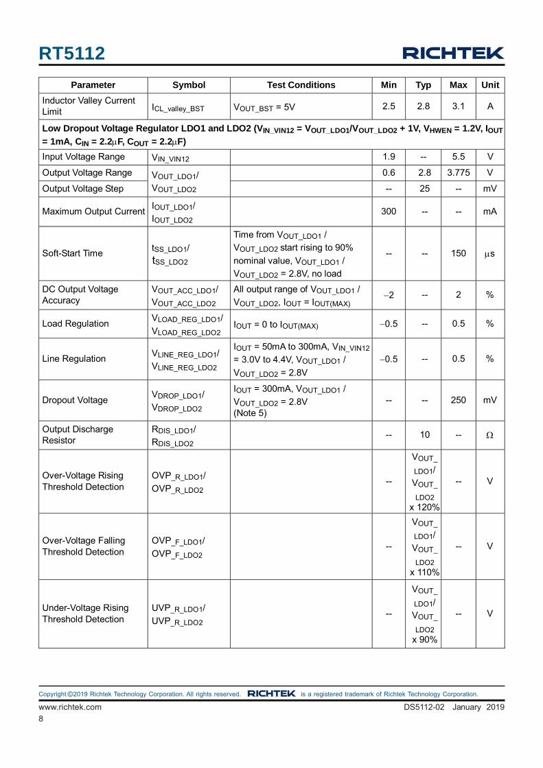
Parameter Symbol Test Conditions Min Typ Max Unit
Inductor Valley Current Limit ICL_valley_BST VOUT_BST = 5V 2.5 2.8 3.1 A
Low Dropout Voltage Regulator LDO1 and LDO2 (VIN_VIN12 = VOUT_LDO1/VOUT_LDO2 + 1V, VHWEN = 1.2V, IOUT
= 1mA, CIN = 2.2F, COUT = 2.2F)
Input Voltage Range VIN_VIN12 1.9 -- 5.5 V
Output Voltage Range VOUT_LDO1/
VOUT_LDO2
0.6 2.8 3.775 V
Output Voltage Step -- 25 -- mV
Maximum Output Current IOUT_LDO1/
IOUT_LDO2 300 -- -- mA
Soft-Start Time tSS_LDO1/
tSS_LDO2
Time from VOUT_LDO1 /
VOUT_LDO2 start rising to 90%
nominal value, VOUT_LDO1 /
VOUT_LDO2 = 2.8V, no load
-- -- 150 s
DC Output Voltage Accuracy
VOUT_ACC_LDO1/
VOUT_ACC_LDO2
All output range of VOUT_LDO1 /
VOUT_LDO2, IOUT = IOUT(MAX) 2 -- 2 %
Load Regulation VLOAD_REG_LDO1/
VLOAD_REG_LDO2 IOUT = 0 to IOUT(MAX) 0.5 -- 0.5 %
Line Regulation VLINE_REG_LDO1/
VLINE_REG_LDO2
IOUT = 50mA to 300mA, VIN_VIN12
= 3.0V to 4.4V, VOUT_LDO1 /
VOUT_LDO2 = 2.8V
0.5 -- 0.5 %
Dropout Voltage VDROP_LDO1/
VDROP_LDO2
IOUT = 300mA, VOUT_LDO1 /
VOUT_LDO2 = 2.8V (Note 5)
-- -- 250 mV
Output Discharge Resistor
RDIS_LDO1/
RDIS_LDO2 -- 10 --
Over-Voltage Rising Threshold Detection
OVP_R_LDO1/
OVP_R_LDO2 --
VOUT_
LDO1/
VOUT_
LDO2
x 120%
-- V
Over-Voltage Falling Threshold Detection
OVP_F_LDO1/
OVP_F_LDO2 --
VOUT_
LDO1/
VOUT_
LDO2
x 110%
-- V
Under-Voltage Rising Threshold Detection
UVP_R_LDO1/
UVP_R_LDO2 --
VOUT_
LDO1/
VOUT_
LDO2
x 90%
-- V

RT5112
9
DS5112-02 January 2019 www.richtek.com
©Copyright 2019 Richtek Technology Corporation. All rights reserved. is a registered trademark of Richtek Technology Corporation.
Parameter Symbol Test Conditions Min Typ Max Unit
Under-Voltage Falling Threshold Detection
UVP_F_LDO1/
UVP_F_LDO2 --
VOUT_
LDO1/
VOUT_
LDO2 x 80%
-- V
Quiescent Current IQ_LDO1/IQ_LDO2 HWEN = 1.2V, IOUT = 0mA -- 22 27
A HWEN = 0.3V (disable) -- 0.1 1
Short Circuit Current Limit
Isc_LDO1/
Isc_LDO2 360 -- -- mA
Current Limit ILimt_LDO1/
ILimt_LDO2
0x01[3:2] = 11 (LDO1 current limit = 360mA), 0x02[3:2] = 11 (LDO2 current limit = 360mA)
360 415 470 mA
Short Protection On Timer
tscp_ON_LDO1/
tscp_ON_LDO2 -- 2 -- ms
Short Protection Off Timer
tscp_OFF_LDO1/
tscp_OFF_LDO2 -- 40 -- ms
Low Dropout Voltage Regulator LDO3 and LDO4 (VIN_VIN3/VIN_VIN4 = VOUT_LDO3/VOUT_LDO4 + 1V, VHWEN =
1.2V, IOUT = 1mA, CIN= 2.2F, COUT = 2.2F)
Input Voltage Range VIN_VIN3/
VIN_VIN4 1.9 -- 5.5 V
Output Voltage Range VOUT_LDO3/
VOUT_LDO4
0.6 1.8 3.775 V
Output Voltage Step -- 25 -- mV
Maximum Output Current IOUT_LDO3/
IOUT_LDO4 300 -- -- mA
Soft-Start Time tSS_LDO3/
tSS_LDO4
Time from VOUT_LDO3 /
VOUT_LDO4 start rising to 90% nominal value, VOUT_LDO3 /
VOUT_LDO4 = 1.8V, no load
-- -- 150 s
DC Output Voltage Accuracy
VOUT_ACC_LDO3/
VOUT_ACC_LDO4
All output range of VOUT_LDO3 /
VOUT_LDO4, IOUT = IOUT(MAX) 2 -- 2 %
Load Regulation VLOAD_REG_LDO3/
VLOAD_REG_LDO4 IOUT = 0 to IOUT(MAX) 0.5 -- 0.5 %
Line Regulation VLINE_REG_LDO3/
VLINE_REG_LDO4
IOUT = 50mA/300mA, VIN_VIN3 /
VIN_VIN4 = 3.0 to 4.4V,
VOUT_LDO3 / VOUT_LDO4 = 1.8V
0.5 -- 0.5 %
Dropout Voltage VDROP_LDO3/
VDROP_LDO4
IOUT = 300mA, VOUT_LDO3 /
VOUT_LDO4 = 1.8V (Note 5)
-- -- 150 mV
Output Discharge Resistor
RDIS_LDO3/
RDIS_LDO4 -- 10 --

RT5112
10
DS5112-02 January 2019www.richtek.com
©Copyright 2019 Richtek Technology Corporation. All rights reserved. is a registered trademark of Richtek Technology Corporation.
Parameter Symbol Test Conditions Min Typ Max Unit
Over-Voltage Rising Threshold Detection
OVP_R_LDO3/
OVP_R_LDO4 --
VOUT
_LDO3/
VOUT
_LDO4 x 120%
-- V
Over-Voltage Falling Threshold Detection
OVP_F_LDO3/
OVP_F_LDO4 --
VOUT
_LDO3/
VOUT
_LDO4 x 110%
-- V
Under-Voltage Rising Threshold Detection
UVP_R_LDO3/
UVP_R_LDO4 --
VOUT
_LDO3/
VOUT
_LDO4 x 90%
-- V
Under-Voltage Falling Threshold Detection
UVP_F_LDO3/
UVP_F_LDO4 --
VOUT
_LDO3/
VOUT
_LDO4 x 80%
-- V
Quiescent Current IQ_LDO3/IQ_LDO4 HWEN = 1.2V, IOUT = 0mA -- 22 27
A HWEN = 0.3V (disable) -- 0.1 1
Short Circuit Current Limit
Isc_LDO3/
Isc_LDO4 360 -- -- mA
Current Limit ILimt_LDO3/
ILimt_LDO4
0x03[3:2] = 11 (LDO3 current limit = 360mA), 0x04[3:2] = 11 (LDO4 current limit = 360mA)
360 415 470 mA
Short Protection On Timer
tscp_ON_LDO3/
tscp_ON_LDO4 -- 2 -- ms
Short Protection Off Timer
tscp_OFF_LDO3/
tscp_OFF_LDO4 -- 40 -- ms
I2C Characteristics
SCL, SDA Low Input Voltage VI
2CIL -- -- 0.4 V
SCL, SDA High Input Voltage VI
2CIH 1.2 -- -- V
SCL, SDA Low Output Voltage VI
2COL -- -- 0.4 V
I2C CLK Frequency fSCL 1 -- -- MHz
I2C Work Voltage VI2Cint -- 1.8 -- V
Input Current Each IO Pin IIN_I2C 10 -- 10 A

RT5112
11
DS5112-02 January 2019 www.richtek.com
©Copyright 2019 Richtek Technology Corporation. All rights reserved. is a registered trademark of Richtek Technology Corporation.
Parameter Symbol Test Conditions Min Typ Max Unit
Data Hold Time tDH_I2C 30 -- -- ns
Data Set-Up Time tDS_I2C 70 -- -- ns
Note 1. Stresses listed as the above "Absolute Maximum Ratings" may cause permanent damage to the device. These are for
stress ratings. Functional operation of the device at these or any other conditions beyond those indicated in the
operational sections of the specifications is not implied. Exposure to absolute maximum rating conditions for extended
periods may remain possibility to affect device reliability.
Note 2. θJA is measured under natural convection (still air) at TA = 25°C with the component mounted on a high effective-
thermal-conductivity four-layer test board on a JEDEC 51-7 thermal measurement standard.
Note 3. Devices are ESD sensitive. Handling precaution is recommended.
Note 4. The device is not guaranteed to function outside its operating conditions.
Note 5. Dropout voltage is the voltage difference between the input and the output at which the output voltage drops to 100 mV
below its nominal value.
System CharacteristicsThe following system specifications are guaranteed by designed and are not performed in production testing.(TA = 25°C, unless otherwise specified.)
Parameter Symbol Test Conditions Min Typ Max Unit
System Parameter
Over-Temperature Warning
OTW 115 125 135 °C
Over-Temperature Warning Hysteresis
OTW_H -- 20 -- °C
Over-Temperature Protection
OTP 130 140 150 °C
Over-Temperature Protection Hysteresis
OTP_H 0x0A[4:3] = 01 -- 20 -- °C
HWEN and BSTEN Control
HWEN Turn On Delay tHWEN_ON HWEN = H to I2C operation available
-- 50 -- s
HWEN Turn Off Delay tHWEN_OFF HWEN = L to I2C operation stop -- 50 -- s
BSTEN Turn On Delay tBSTEN_ON BSTEN to Boost voltage start rising
-- 225 -- s
BSTEN Turn Off Delay tBSTEN_OFF BSTEN off to Boost switch stop -- 16 -- s
Step Down Buck Converter (VIN_B = 3.8V, C1 = C2 = 10F, L1 = 1H)
Maximum Output Current IOUT_BUCK 1.2 -- -- A
Load Regulation VLOAD_REG_BUCK CCM, VOUT_BUCK = 1.1V -- -- 1.5 %
Line Regulation VLINE_REG_BUCK CCM, IOUT = 50/300/1200mA,
VOUT_BUCK = 1.1V, VIN_B = 3.0V to 4.4V
-- -- 1.5 %

RT5112
12
DS5112-02 January 2019www.richtek.com
©Copyright 2019 Richtek Technology Corporation. All rights reserved. is a registered trademark of Richtek Technology Corporation.
Parameter Symbol Test Conditions Min Typ Max Unit
Output Ripple VRIPPLE_BUCK
CCM, IOUT = 300mA, VOUT_BUCK
= 1.1V, VIN_B < 4.35V -- -- 10
mV PFM, VOUT_BUCK = 1.1V, VIN_B < 4.35V
-- 30 40
Soft-Start Time tSS_BUCK
0x09[7:6] = 10, time from
VOUT_BUCK = 0V rising to 90%
nominal value, VOUT_BUCK = 1.1V, no load
-- 235 -- s
Load Transient VTRAN_BUCK VOUT_BUCK = 1.1V, 20 to 80%
IOUT(MAX), 1s, recovery time < 10s
-- -- 70 mV
Efficiency Eff_BUCK VOUT_BUCK = 1.1V, IOUT = 200mA to 600mA
85 -- -- %
Step Up Boost Converter (VIN_BST = 3.8V, C3 = 10F, C4 = 22F, L2 = 0.47H)
Maximum Output Current IOUT_BST VIN_BST = 2.8V, VOUT_BST = 5V 1 -- -- A
Soft-Start Time tSS_BST
0x05[5:4] = 00, time from
VOUT_BST = 0V rising to 90%
nominal value, VOUT_BST = 5V, no load
-- -- 580 s
Start Up Time tSTART_BST
Time from BSTEN = H to
VOUT_BST rising to 90% nominal
value, VOUT_BST = 5V, no load
-- -- 700 s
Load Regulation VLOAD_REG_BST CCM, VOUT_BST = 5V -- -- 1.5 %
Line Regulation VLINE_REG_BST CCM, IOUT = 50/1000mA,
VIN_BST = 3V to 4.4V, VOUT_BST = 5V
-- -- 1.5 %
Output Ripple VRIPPLE_BST
CCM, IOUT = 500mA, VIN_BST =
3.4V to 4.4V, VOUT_BST = 5V -- -- 40
mVPFM, VIN_BST = 3.4V to 4.4V,
VOUT_BST = 5V -- 40 80
Load Transient VTRAN_BST VOUT_BST = 5V, 20 to 80%
IOUT(MAX), 2s, recovery time < 30s
-- 100 150 mV
Power Efficiency Eff_BST
VOUT_BST = 5V, VIN_BST = 3.4V,
IOUT_BST = 10mA -- 88 --
% VOUT_BST = 5V, VIN_BST = 3.4V,
IOUT_BST = 600mA -- 90 --
VOUT_BST = 5V, VIN_BST = 3.4V,
IOUT_BST = 1A -- 84 --
Linear Charge Hiccup On Time tLC_ON During linear charge state -- 10 -- ms

RT5112
13
DS5112-02 January 2019 www.richtek.com
©Copyright 2019 Richtek Technology Corporation. All rights reserved. is a registered trademark of Richtek Technology Corporation.
Parameter Symbol Test Conditions Min Typ Max Unit
Linear Charge Hiccup Off Time tLC_OFF Restart linear charge -- 100 -- ms
ABS Output Over-Voltage Rising Threshold OVP_R_ABS_BST Stop switch -- 6.5 -- V
ABS Output Over-Voltage Falling Threshold OVP_F_ABS_BST Start switch -- 5.8 -- V
Low Dropout Voltage Regulator LDO1 and LDO2 (VIN_VIN12 = VOUT_LDO1/VOUT_LDO2 + 1V, VHWEN = 1.2V, IOUT
= 1mA, CIN = 2.2F, COUT = 2.2F)
Output Ripple Voltage VRIPPLE_LDO1/
VRIPPLE_LDO2
IOUT = 0 to IOUT(MAX),
VOUT_LDO1/VOUT_LDO2 = 2.8V -- -- 10 mV
Load Transient VTRAN_LDO1/
VTRAN_LDO2
IOUT = 1mA to 150mA, 150mA/s,
VOUT_LDO1/VOUT_LDO2 = 2.8V -- -- 50 mV
Power Supply Rejection Ratio
PSRR_LDO1/
PSRR_LDO2
VIN_VIN12 = 3.4V, f = 1kHz, IOUT =
100mA, VOUT_LDO1/VOUT_LDO2 = 2.8V
70 -- --
dB VIN_VIN12 = 3.4V, f = 100kHz,
IOUT = 100mA,
VOUT_LDO1/VOUT_LDO2 = 2.8V
40 -- --
Output Noise Voltage eN_LDO1/
eN_LDO2
100Hz to 100kHz, IOUT = 100mA,
VOUT_LDO1/VOUT_LDO2 = 2.8V -- 50 -- V
Low Dropout Voltage Regulator LDO3 and LDO4 (VIN_VIN3/VIN_VIN4 = VOUT_LDO3/VOUT_LDO4 + 1V, VHWEN =
1.2V, IOUT = 1mA, CIN = 2.2F, COUT = 2.2F)
Output Ripple Voltage VRIPPLE_LDO3/
VRIPPLE_LDO4
IOUT = 0 to IOUT(MAX),
VOUT_LDO3/VOUT_LDO4 = 1.8V -- -- 10 mV
Load Transient VTRAN_LDO3/
VTRAN_LDO4
IOUT = 1mA to 150mA, 150mA/s,
VOUT_LDO3/VOUT_LDO4 = 1.8V -- -- 50 mV
Power Supply Rejection Ratio
PSRR_LDO3/
PSRR_LDO4
VIN_VIN3 / VIN_VIN4 = 1.95V,
f = 1kHz, IOUT = 100mA,
VOUT_LDO3/VOUT_LDO4 = 1.8V
50 -- --
dB VIN_VIN3 / VIN_VIN4 = 1.95V,
f = 10kHz, IOUT = 100mA,
VOUT_LDO3/VOUT_LDO4 = 1.8V
40 -- --
Output Noise Voltage eN_LDO3/ eN_LDO4
100Hz to 100kHz, IOUT = 100mA,
VOUT_LDO3/VOUT_LDO4 = 1.8V -- 50 -- V

RT5112
14
DS5112-02 January 2019www.richtek.com
©Copyright 2019 Richtek Technology Corporation. All rights reserved. is a registered trademark of Richtek Technology Corporation.
Buck Quiescent Current vs. Input Voltage
6
7
8
9
10
11
12
2.5 3.0 3.5 4.0 4.5
Input Voltage (V)
Bu
ck Q
uie
sce
nt C
urr
en
t (μ
A) 1
Typical Operating Characteristics
Shutdown Current vs. Temperature
0.0
0.2
0.4
0.6
0.8
1.0
-50 -25 0 25 50 75 100 125
Temperature (°C)
Sh
utd
ow
n C
urr
en
t (μ
A) 1
Buck Quiescent Current vs. Temperature
6
7
8
9
10
11
12
-50 -25 0 25 50 75 100 125
Temperature (°C)
Bu
ck Q
uie
sce
nt C
urr
en
t (μ
A) 1
Buck Efficiency
50
60
70
80
90
100
0.0 0.2 0.4 0.6 0.8 1.0 1.2
Load Current (A)
Effi
cie
ncy
(%
)
Buck Load Regulation
1.08
1.09
1.10
1.11
1.12
1.13
0.0 0.2 0.4 0.6 0.8 1.0 1.2
Load Current (A)
Ou
tpu
t Vo
ltag
e (
V)
Buck Output Voltage Ripple vs. Load Current
0
5
10
15
20
25
30
0.0 0.2 0.4 0.6 0.8 1.0 1.2
Load Current (A)
Bu
ck O
utp
ut V
olta
ge
Rip
ple
(m
Vp
p) 1
HWEN = L, BSTEN = L VBUCK = 1.1V, Temperature = 25°C
VINB = 3.8V, VBUCK = 1.1V VBUCK = 1.1V
VINB = 3.4VVINB = 3.8VVINB = 4.35V
VINB = 4.35VVINB = 3.8VVINB = 3.4V
VBUCK = 1.1V
VINB = 4.35VVINB = 3.8VVINB = 3.4V
VBUCK = 1.1V

RT5112
15
DS5112-02 January 2019 www.richtek.com
©Copyright 2019 Richtek Technology Corporation. All rights reserved. is a registered trademark of Richtek Technology Corporation.
Buck Switching Frequency vs. Load Current
0.0
0.5
1.0
1.5
2.0
2.5
3.0
0.0 0.2 0.4 0.6 0.8 1.0 1.2
Load Current (A)
Bu
ck S
witc
hin
g F
req
ue
ncy
(M
Hz)
1
Boost Quiescent Current vs. Input Voltage
10
11
12
13
14
15
16
17
18
2.5 3.0 3.5 4.0 4.5
Input Voltage (V)
Bo
ost
Qu
iesc
en
t Cu
rre
nt (μ
A) 1
Boost Quiescent Current vs. Temperature
10
11
12
13
14
15
16
17
18
-50 -25 0 25 50 75 100 125
Temperature (°C)
Bo
ost
Qu
iesc
en
t Cu
rre
nt (μ
A) 1
VBUCK = 1.1V
VINB = 4.35VVINB = 3.8VVINB = 3.4V
VBOOST = 5V, Temperature = 25°C VIN = 3.8V, VBOOST = 5V
Buck Power On
Time (200μs/Div)
SCL(2V/Div)
VIN
(1V/Div)
IIN
(50mA/Div)
Buck Power Off
Time (2ms/Div)
Buck Load Transient
Time (50μs/Div)
VINB = 3.8V, VBUCK = 1.1V, IBUCK = 0mA
VINB = 3.8V, VBUCK = 1.1V, IBUCK = 0mA
VINB = 3.8V, VBUCK = 1.1V,IBUCK = 240mA to 960mA (tR = tF = 1μs)
VBUCK
(500mV/Div)
SCL(2V/Div)
VIN
(1V/Div)
IIN
(50mA/Div)
VBUCK
(500mV/Div)IBUCK
(200mA/Div)
VBUCK
(50mV/Div)

RT5112
16
DS5112-02 January 2019www.richtek.com
©Copyright 2019 Richtek Technology Corporation. All rights reserved. is a registered trademark of Richtek Technology Corporation.
Boost Load Regulation
4.90
4.92
4.94
4.96
4.98
5.00
5.02
5.04
5.06
5.08
5.10
0.0 0.2 0.4 0.6 0.8 1.0
Load Current (A)
Ou
tpu
t Vo
ltag
e (
V)
Boost Load Regulation
4.90
4.92
4.94
4.96
4.98
5.00
5.02
5.04
5.06
5.08
5.10
0.0 0.2 0.4 0.6 0.8 1.0
Load Current (A)
Ou
tpu
t Vo
ltag
e (
V)
Boost Efficiency
50
55
60
65
70
75
80
85
90
95
100
0.0 0.2 0.4 0.6 0.8 1.0
Load Current (A)
Effi
cie
ncy
(%
)
Boost Efficiency
50
55
60
65
70
75
80
85
90
95
100
0.0 0.2 0.4 0.6 0.8 1.0
Load Current (A)
Effi
cie
ncy
(%
)
Boost Output Voltage Ripple vs. Load Current
0
10
20
30
40
50
60
70
80
0.0 0.2 0.4 0.6 0.8 1.0
Load Current (A)
Bo
ost
Ou
tpu
t Vo
ltag
e R
ipp
le (
mV
pp
)
Boost Output Voltage Ripple vs. Load Current
0
10
20
30
40
50
60
70
80
0.0 0.2 0.4 0.6 0.8 1.0
Load Current (A)
Bo
ost
Ou
tpu
t Vo
ltag
e R
ipp
le (
mV
pp
)
VBOOST = 5V, NFCAuto (0x05[6] = 1, 0x39[2] = 0)
VINB = 4.35VVINB = 3.8VVINB = 3.4V
VINB = 4.35VVINB = 3.8VVINB = 3.4V
VBOOST = 5V, NFCFCCM (0x05[6] = 0, 0x39[2] = 1)
VINB = 4.35VVINB = 3.8VVINB = 3.4V
VBOOST = 5V, NFCAuto (0x05[6] = 1, 0x39[2] = 0) VBOOST = 5V, NFCFCCM (0x05[6] = 0, 0x39[2] = 1)
VINB = 4.35VVINB = 3.8VVINB = 3.4V
VINB = 4.35VVINB = 3.8VVINB = 3.4V
VINB = 4.35VVINB = 3.8VVINB = 3.4V
VBOOST = 5V, NFCAuto (0x05[6] = 1, 0x39[2] = 0) VBOOST = 5V, NFCFCCM (0x05[6] = 0, 0x39[2] = 1)

RT5112
17
DS5112-02 January 2019 www.richtek.com
©Copyright 2019 Richtek Technology Corporation. All rights reserved. is a registered trademark of Richtek Technology Corporation.
Boost Switching Frequency vs. Load Current
0
500
1000
1500
2000
2500
3000
3500
0.0 0.2 0.4 0.6 0.8 1.0
Load Current (A)
Bo
ost
Sw
itch
ing
Fre
qu
en
cy (
MH
z) 1
Boost Switching Frequency vs. Load Current
0
500
1000
1500
2000
2500
3000
3500
0.0 0.2 0.4 0.6 0.8 1.0
Load Current (A)
Bo
ost
Sw
itch
ing
Fre
qu
en
cy (
MH
z) 1
VINB = 3.4VVINB = 3.8VVINB = 4.35V
VBOOST = 5V, NFCAuto (0x05[6] = 1, 0x39[2] = 0) VBOOST = 5V, NFCFCCM (0x05[6] = 0, 0x39[2] = 1)
VINB = 3.4VVINB = 3.8VVINB = 4.35V
Time (200μs/Div)
Boost Register Power Off
Time (2ms/Div)
Boost BSTEN Power On
Time (200μs/Div)
BSTEN(2V/Div)
Boost BSTEN Power Off
Time (2ms/Div)
Boost Register Power On
SCL(2V/Div)
VIN
(1V/Div)
IIN
(200mA/Div)
VBOOST
(2V/Div)
VIN = 3.8V, VBOOST = 5V, IBOOST = 0mA
SCL(2V/Div)
VIN
(1V/Div)
IIN
(200mA/Div)
VBOOST
(2V/Div)
VIN = 3.8V, VBOOST = 5V, IBOOST = 0mA
VIN
(1V/Div)
IIN
(200mA/Div)
VBOOST
(2V/Div)
VIN = 3.8V, VBOOST = 5V, IBOOST = 0mA
BSTEN(2V/Div)
VIN
(1V/Div)
IIN
(200mA/Div)
VBOOST
(2V/Div)
VIN = 3.8V, VBOOST = 5V, IBOOST = 0mA

RT5112
18
DS5112-02 January 2019www.richtek.com
©Copyright 2019 Richtek Technology Corporation. All rights reserved. is a registered trademark of Richtek Technology Corporation.
LDO Quiescent Current vs. Input Voltage
20
21
22
23
24
25
2.5 3.0 3.5 4.0 4.5 5.0 5.5
Input Voltage (V)
LD
O Q
uie
sce
nt C
urr
en
t (μ
A) 1
LDO Quiescent Current vs. Temperature
16
18
20
22
24
26
28
30
-50 -25 0 25 50 75 100 125
Temperature (°C)
LD
O Q
uie
sce
nt C
urr
en
t (μ
A) 1
LDO1 Load Regulation
2.786
2.788
2.790
2.792
2.794
2.796
2.798
2.800
2.802
0.00 0.05 0.10 0.15 0.20 0.25 0.30
Load Current (A)
Ou
tpu
t Vo
ltag
e (
V)
LDO2 Load Regulation
2.786
2.788
2.790
2.792
2.794
2.796
2.798
2.800
2.802
0.00 0.05 0.10 0.15 0.20 0.25 0.30
Load Current (A)
Ou
tpu
t Vo
ltag
e (
V)
LDO4LDO3LDO2LDO1
VLDO1/VLDO2 = 2.8V, VLDO3/VLDO4 = 1.8V,Temperature = 25°C
VIN12/VIN3/VIN4 = 3.8V,VLDO1/VLDO2 = 2.8V, VLDO3/VLDO4 = 1.8V
LDO4LDO3LDO2LDO1
VIN12 = 4.35VVIN12 = 3.8VVIN12 = 3.4VVIN12 = 3V
VLDO1 = 2.8V VLDO2 = 2.8V
VIN12 = 4.35VVIN12 = 3.8VVIN12 = 3.4VVIN12 = 3V
Boost Load Transient
Time (200μs/Div)
VIN = 3.8V, VBOOST = 5V,IBOOST = 200mA to 800mA (tR = tF = 2μs),
NFCAuto (0x05[6] = 1, 0x39[2] = 0)
IBOOST
(200mA/Div)
VBOOST
(100mV/Div)
Boost Load Transient
Time (200μs/Div)
VIN = 3.8V, VBOOST = 5V,IBOOST = 200mA to 800mA (tR = tF = 2μs),
NFCFCCM (0x05[6] = 0, 0x39[2] = 1)IBOOST
(200mA/Div)
VBOOST
(100mV/Div)

RT5112
19
DS5112-02 January 2019 www.richtek.com
©Copyright 2019 Richtek Technology Corporation. All rights reserved. is a registered trademark of Richtek Technology Corporation.
LDO3 Dropout Voltage vs. Load Current
0
20
40
60
80
100
120
140
0 50 100 150 200 250 300
Load Current (A)
LD
O3
Dro
po
ut V
olta
ge
(m
V)
LDO4 Dropout Voltage vs. Load Current
0
20
40
60
80
100
120
140
0 50 100 150 200 250 300
Load Current (A)
LD
O4
Dro
po
ut V
olta
ge
(m
V)
LDO2 Dropout Voltage vs. Load Current
0
20
40
60
80
100
0 50 100 150 200 250 300
Load Current (A)
LD
O2
Dro
po
ut V
olta
ge
(m
V)
LDO1 Dropout Voltage vs. Load Current
0
20
40
60
80
100
0 50 100 150 200 250 300
Load Current (A)
LD
O1
Dro
po
ut V
olta
ge
(m
V)
LDO3 Load Regulation
1.784
1.786
1.788
1.790
1.792
1.794
1.796
1.798
0.00 0.05 0.10 0.15 0.20 0.25 0.30
Load Current (A)
Ou
tpu
t Vo
ltag
e (
V)
LDO4 Load Regulation
1.784
1.786
1.788
1.790
1.792
1.794
1.796
1.798
0.00 0.05 0.10 0.15 0.20 0.25 0.30
Load Current (A)
Ou
tpu
t Vo
ltag
e (
V)
VLDO3 = 1.8V
VIN3 = 4.35VVIN3 = 3.8VVIN3 = 3VVIN3 = 2.8VVIN3 = 2.5VVIN3 = 1.95V
VLDO4 = 1.8V
VIN4 = 4.35VVIN4 = 3.8VVIN4 = 3VVIN4 = 2.8VVIN4 = 2.5VVIN4 = 1.95V
VLDO1 = 2.8V
85°C25°C
-40°C
VLDO2 = 2.8V
85°C25°C
-40°C
VLDO3 = 1.8V
85°C25°C
-40°C
VLDO4 = 1.8V
85°C25°C
-40°C

RT5112
20
DS5112-02 January 2019www.richtek.com
©Copyright 2019 Richtek Technology Corporation. All rights reserved. is a registered trademark of Richtek Technology Corporation.
LDO3/4 PSRR
-100
-80
-60
-40
-20
0
20
100 1000 10000 100000 1000000 10000000
Frequency (Hz)
PS
RR
(d
B)
LDO1/2 Output Noise
0.01
0.1
1
10
100 1000 10000 100000
Frequency (Hz)
No
ise
(μ
V/s
qrt
(Hz)
)
LDO3/4 Output Noise
0.01
0.1
1
10
100 1000 10000 100000
Frequency (Hz)
No
ise
(μ
V/s
qrt
(Hz)
)
LDO3LDO4
VIN3/VIN4 = 1.95V, VLDO3/VLDO4 = 1.8V,ILDO3/ILDO4 = 100mA
LDO1LDO2
VLDO1/VLDO2 = 2.8V, ILDO1/ILDO2 = 100mA
LDO3LDO4
VLDO3/VLDO4 = 1.8V, ILDO3/ILDO4 = 100mA
LDO1 Power On
Time (100μs/Div)
SCL(2V/Div)
LDO1 Power Off
Time (100μs/Div)
VIN
(1V/Div)
IIN
(50mA/Div)
VLDO1
(1V/Div)VIN = 3.8V, VIN12 = 3.8V,
VLDO1 = 2.8V, ILDO1 = 0mA
SCL(2V/Div)
IIN
(50mA/Div)
VLDO1
(1V/Div)
VIN = 3.8V, VIN12 = 3.8V,VLDO1 = 2.8V, ILDO1 = 0mA
LDO1/2 PSRR
-100
-80
-60
-40
-20
0
20
100 1000 10000 100000 1000000 10000000
Frequency (Hz)
PS
RR
(d
B)
LDO1LDO2
VIN12 = 3.4V, VLDO1/VLDO2 = 2.8V,ILDO1/ILDO2 = 100mA
VIN
(1V/Div)

RT5112
21
DS5112-02 January 2019 www.richtek.com
©Copyright 2019 Richtek Technology Corporation. All rights reserved. is a registered trademark of Richtek Technology Corporation.
LDO2 Power On
Time (100μs/Div)
LDO2 Power Off
Time (100μs/Div)
LDO3 Power On
Time (100μs/Div)
LDO3 Power Off
Time (100μs/Div)
LDO4 Power On
Time (100μs/Div)
LDO4 Power Off
Time (100μs/Div)
SCL(2V/Div)
IIN
(50mA/Div)
VLDO2
(1V/Div)VIN = 3.8V, VIN12 = 3.8V,
VLDO2 = 2.8V, ILDO2 = 0mA
SCL(2V/Div)
IIN
(50mA/Div)
VLDO2
(1V/Div)
VIN = 3.8V, VIN12 = 3.8V,VLDO2 = 2.8V, ILDO2 = 0mA
SCL(2V/Div)
IIN
(50mA/Div)
VLDO3
(500mV/Div)VIN = 3.8V, VIN3 = 2.8V,
VLDO3 = 1.8V, ILDO3 = 0mA
SCL(2V/Div)
IIN
(50mA/Div)
VIN = 3.8V, VIN3 = 2.8V,VLDO3 = 1.8V, ILDO3 = 0mA
SCL(2V/Div)
IIN
(50mA/Div)
VIN = 3.8V, VIN4 = 2.8V,VLDO4 = 1.8V, ILDO4 = 0mA
SCL(2V/Div)
IIN
(50mA/Div)
VIN = 3.8V, VIN4 = 2.8V,VLDO4 = 1.8V, ILDO4 = 0mA
VIN
(1V/Div)VIN
(1V/Div)
VIN
(1V/Div)
VIN
(1V/Div)VLDO3
(500mV/Div)
VIN
(1V/Div)
VIN
(1V/Div)
VLDO4
(500mV/Div)
VLDO4
(500mV/Div)

RT5112
22
DS5112-02 January 2019www.richtek.com
©Copyright 2019 Richtek Technology Corporation. All rights reserved. is a registered trademark of Richtek Technology Corporation.
LDO2 Load Transient
Time (5μs/Div)
LDO3 Load Transient
Time (5μs/Div)
LDO4 Load Transient
Time (5μs/Div)
VIN4 = 2.8V, VLDO4 = 1.8V,ILDO4 = 1mA to 150mA (tR = tF = 1μs)
ILDO4
(50mA/Div)
VLDO4
(10mV/Div)
VIN12 = 3.8V, VLDO2 = 2.8V,ILDO2 = 1mA to 150mA (tR = tF = 1μs)
ILDO2
(50mA/Div)
VLDO2
(10mV/Div)
VIN3 = 2.8V, VLDO3 = 1.8V,ILDO3 = 1mA to 150mA (tR = tF = 1μs)
ILDO3
(50mA/Div)
VLDO3
(10mV/Div)
LDO1 Load Transient
Time (5μs/Div)
VIN12 = 3.8V, VLDO1 = 2.8V,ILDO1 = 1mA to 150mA (tR = tF = 1μs)
ILDO1
(50mA/Div)
VLDO1
(10mV/Div)
RT5112
23
DS5112-02 January 2019 www.richtek.com
©Copyright 2019 Richtek Technology Corporation. All rights reserved. is a registered trademark of Richtek Technology Corporation.
Application Information
The RT5112 is a smart power-management integrated
circuit (PMIC), which includes a Buck converter, a Boost
converter and four LDOs.
System Under-Voltage Protection and Over-Voltage
Protection
The device does not operate with VSYS voltages below the
Under-Voltage Lock Out (UVLO) level. There is a typical
100mV hysteresis implemented to avoid unstable on/ off
behavior. The RT5112 is initialized in its default state after
VSYS voltage recovers from UVLO. When VSYS voltage
reaches the Over Voltage Protection level, the RT5112
will disable Buck converter immediately to protect next
stage circuit input. The VSYS UV and OV status bits and
interrupt bits will be set, and INTRB pin will be pulled low
with corresponding to protection detected.
Thermal Protection
The RT5112 features over-temperature warning (OTW) and
over-temperature protection (OTP). The OTW status bit
and interrupt bit are set and INTRB pin will be pulled low
when the junction temperature is higher than typical
125°C. If the junction temperature further exceeds typical
160°C, OTP will be triggered to shut down the device.
When the RT5112 recovers from OTP, it can re-start in
three configurations with register 0x0A[4:3] bits.
0x0A[4:3] = 00, the RT5112 is manual re-start with
default register values.
0x0A[4:3] = 01, the RT5112 is auto recovery with last
register values before OTP.
0x0A[4:3] = 10, the RT5112 is latched off. Re-set VIN or
HWEN or BSTEN (if Boost is controlled by BSTEN) to
re-start the RT5112 with default register values.
Enable and Disable Control
The HWEN pin controls the RT5112 start up without
enabling channels. If HWEN pin is at low state, the RT5112
is in power down mode and I2C will return NACK to any
request. Only when HWEN pin is at high state, all channels
are controllable via I2C with corresponding ENABLE
command. The BSTEN pin is only used to hardware control
Boost converter enable or disable. There are both built-in
resistors on HWEN and BSTEN pins to keep at low state
if pins are left unconnected.
The below tables provide channels state with combinations
of different ENABLE pins and register EN bits.
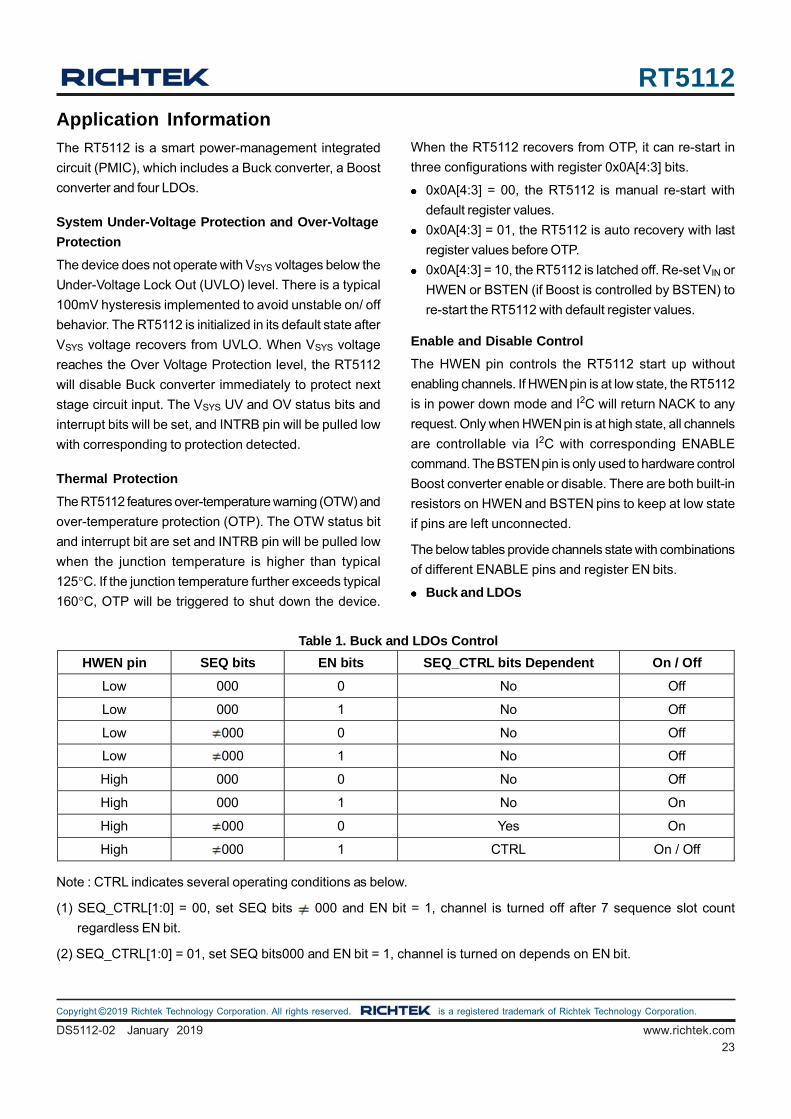
Buck and LDOs
HWEN pin SEQ bits EN bits SEQ_CTRL bits Dependent On / Off
Low 000 0 No Off
Low 000 1 No Off
Low 000 0 No Off
Low 000 1 No Off
High 000 0 No Off
High 000 1 No On
High 000 0 Yes On
High 000 1 CTRL On / Off
Table 1. Buck and LDOs Control
Note : CTRL indicates several operating conditions as below.
(1) SEQ_CTRL[1:0] = 00, set SEQ bits 000 and EN bit = 1, channel is turned off after 7 sequence slot count
regardless EN bit.
(2) SEQ_CTRL[1:0] = 01, set SEQ bits000 and EN bit = 1, channel is turned on depends on EN bit.

RT5112
24
DS5112-02 January 2019www.richtek.com
©Copyright 2019 Richtek Technology Corporation. All rights reserved. is a registered trademark of Richtek Technology Corporation.
Sequence Control Setting
The RT5112 Buck and LDOs sequence on/off control
setting can be programmed via I2C with dedicated
registers as below.
Sequence (7 slots)
Register 0x00[6:4] is used to control Buck
sequence on/off slot.
Registers 0x01[6:4], 0x02[6:4], 0x03[6:4] and
0x04[6:4] are used to control LDOs sequence on/
off slots.
Slot Interval Time
Register 0x09[7:6] is used to control interval time
between each slot.
Soft Start Time
Register 0x09[7:6] is used to control Buck
sequence on soft start time.
Register 0x11[1:0] is used to control LDOs
sequence on soft start time.
Sequence Control
Register 0x09[5:4] = 00 is used to enable sequence
off with sequence setting 000.
Register 0x09[5:4] = 01 is used to enable sequence
on with sequence setting000.
Note :
(1) Any changes in Sequence (7 slots), slot interval
time and soft-start time during sequence on or off
procedure is not valid and will not modify the RT5112
setting.
(2) Channel setting (output voltage, current limit...etc.)
is fixed during on or off sequence.
(3) Register 0x09[5:4] = 11 will turn off all channels
immediately.
(4) HWEN = 0 will turn off all channels and the RT5112
enters into power down mode.
Normal Control Setting
When register bits 0x09[5:4] = 10, the Buck and LDOs
on/off control depends on channel Enable bit.
Register 0x00[7] is used to control Buck on/off.
Register 0x01[7], 0x02[7], 0x03[7] and 0x04[7] are
used to control LDOs on/off.
HWEN
SEQ_CTRL = 10
BUCK
LDO1
LDO2
LDO3
LDO4
SLOT1 SLOT2 SLOT3 SLOT4 SLOT5 SLOT6 SLOT7 SLOT7 SLOT6 SLOT5 SLOT4 SLOT3 SLOT2 SLOT1
SEQ_CTRL = 01 SEQ_CTRL = 00
BUCK_DELAYLDOX_DELAY
Figure 1.
Example for sequence on/off with BUCK assign to SLOT1, LDO1 assign to SLOT2, LDO2 assign to SLOT3, LDO3
assign to SLOT4 and LDO4 assign to SLOT5.

RT5112
25
DS5112-02 January 2019 www.richtek.com
©Copyright 2019 Richtek Technology Corporation. All rights reserved. is a registered trademark of Richtek Technology Corporation.
HWEN
SEQ_CTRL = 10
BUCK
LDO1
LDO2
LDO3
LDO4
SLOT1 SLOT2 SLOT3 SLOT4 SLOT5 SLOT6 SLOT7 SLOT7 SLOT6 SLOT5 SLOT4 SLOT3 SLOT2 SLOT1
SEQ_CTRL = 01 SEQ_CTRL = 00
BUCK_DELAYLDOX_DELAY
Figure 2.
Example for sequence on/off with BUCK assign to SLOT1, LDO1 assign to SLOT3, LDO2 assign to SLOT3, LDO3
assign to SLOT7 and LDO4 assign to SLOT5.
Example for sequence slot change when on procedure. LDO2 assign from SLOT3 to SLOT5, LDO3 assign from SLOT4
to SLOT6 and LDO4 assign from SLOT5 to SLOT7. There is no influence with on procedure and new setting will
executed after on sequence finish.
Figure 3.
HWEN
SEQ_CTRL = 10
BUCK
LDO1
LDO2
LDO3
LDO4
SLOT1 SLOT2 SLOT3 SLOT4 SLOT5 SLOT6 SLOT7 SLOT7 SLOT6 SLOT5 SLOT4 SLOT3 SLOT2 SLOT1
SEQ_CTRL = 01 SEQ_CTRL = 00
BUCK_DELAYLDOX_DELAY LDO2_DELAY, LDO3_DELAY and LDO4_DELAY change setting

RT5112
26
DS5112-02 January 2019www.richtek.com
©Copyright 2019 Richtek Technology Corporation. All rights reserved. is a registered trademark of Richtek Technology Corporation.
HWEN
SEQ_CTRL = 10
BUCK
LDO1
LDO2
LDO3
LDO4
SLOT1 SLOT2 SLOT3 SLOT4 SLOT5 SLOT6 SLOT7
SEQ_CTRL = 01
BUCK_DELAYLDOX_DELAY
Figure 4.
Example for sequence on is interrupted by HWEN signal low. The RT5112 turns off all channels immediately.
HWEN
SEQ_CTRL = 10
BUCK
LDO1
LDO2
LDO3
LDO4
SLOT1 SLOT2 SLOT3 SLOT4 SLOT5 SLOT6 SLOT7 SLOT7 SLOT6 SLOT5 SLOT4 SLOT3 SLOT2 SLOT1
SEQ_CTRL = 01 SEQ_CTRL = 00
BUCK_DELAYLDOX_DELAY
Figure 5.
Example for sequence off is interrupted by HWEN signal low. The RT5112 turns off all channels immediately.

RT5112
27
DS5112-02 January 2019 www.richtek.com
©Copyright 2019 Richtek Technology Corporation. All rights reserved. is a registered trademark of Richtek Technology Corporation.
HWEN
SEQ_CTRL = 10
BUCK
LDO1
LDO2
LDO3
LDO4
SLOT1 SLOT2 SLOT3 SLOT4 SLOT5 SLOT6 SLOT7 SLOT7 SLOT6 SLOT5 SLOT4 SLOT3 SLOT2 SLOT1
SEQ_CTRL = 01 SEQ_CTRL = 00
LDOX_DELAY
BUCK_EN
LDO1_EN
HWEN
SEQ_CTRL = 10
BUCK
LDO1
LDO2
LDO3
LDO4
SLOT1 SLOT2 SLOT3 SLOT4 SLOT5 SLOT6 SLOT7 SLOT7 SLOT6 SLOT5 SLOT4 SLOT3 SLOT2 SLOT1
SEQ_CTRL = 01 SEQ_CTRL = 10
LDOX_DELAY
BUCK_EN
LDO1_EN
Figure 6.
Figure 7.
Example for sequence control SEQ_CTRL change from 01 to 00. LDO2, LDO3, LDO4 are sequence off and LDO1 is
turned off by itself enable bit. BUCK1 is turned off after 7 sequence slot count even itself enable bit is at high state.
Example for sequence control SEQ_CTRL change from 01 to 10. LDO2, LDO3, LDO4 are turned off and state of BUCK,
LDO1 depends on itself enable bit.

RT5112
28
DS5112-02 January 2019www.richtek.com
©Copyright 2019 Richtek Technology Corporation. All rights reserved. is a registered trademark of Richtek Technology Corporation.
HWEN
SEQ_CTRL = 10
BUCK
LDO1
LDO2
LDO3
LDO4
SLOT1 SLOT2 SLOT3 SLOT4 SLOT5 SLOT6 SLOT7 SLOT7 SLOT6 SLOT5 SLOT4 SLOT3 SLOT2 SLOT1
SEQ_CTRL = 01 SEQ_CTRL = 11
LDOX_DELAY
BUCK_EN
LDO1_EN
Figure 8.
Example for sequence control SEQ_CTRL change from 01 to 11. All channels are turned off immediately.
Boost
HWEN pin BSTEN pin EN bits On / Off
Low Low 0 Off
Low Low 1 Off
Low High 0 On
Low High 1 On
High Low 0 Off
High Low 1 On
High High 0 On
High High 1 On
Table 2. Boost Control
Note : The Boost Control table above shows that the Boost operation requires either BSTEN pin to be high or a
combination of HWEN pin high and one of the EN bits in register 0x08 needs to be set to 1.
Normal Control Setting
The RT5112 Boost on/off control setting can be programmed via I2C with dedicated registers or external BSTEN pin.
BSTEN pin to hardware control on/off.
Register 0x08[7] to 0x08[0], each bit is able to software control on/off.
RT5112
29
DS5112-02 January 2019 www.richtek.com
©Copyright 2019 Richtek Technology Corporation. All rights reserved. is a registered trademark of Richtek Technology Corporation.
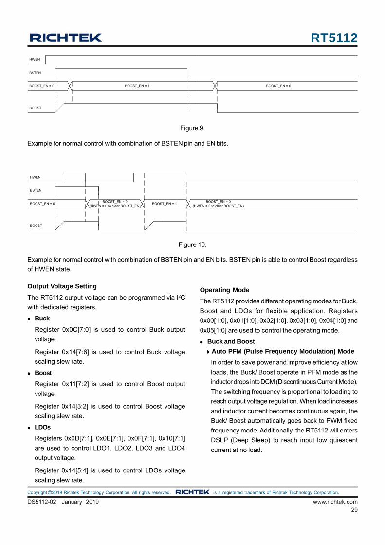
HWEN
BOOST_EN = 0
BOOST
BOOST_EN = 1 BOOST_EN = 0
BSTEN
HWEN
BOOST_EN = 0
BOOST
BOOST_EN = 0(HWEN = 0 to clear BOOST_EN)
BSTEN
BOOST_EN = 1BOOST_EN = 0
(HWEN = 0 to clear BOOST_EN)
Figure 9.
Figure 10.
Example for normal control with combination of BSTEN pin and EN bits.
Example for normal control with combination of BSTEN pin and EN bits. BSTEN pin is able to control Boost regardless
of HWEN state.
Output Voltage Setting
The RT5112 output voltage can be programmed via I2C
with dedicated registers.
Buck
Register 0x0C[7:0] is used to control Buck output
voltage.
Register 0x14[7:6] is used to control Buck voltage
scaling slew rate.
Boost
Register 0x11[7:2] is used to control Boost output
voltage.
Register 0x14[3:2] is used to control Boost voltage
scaling slew rate.
LDOs
Registers 0x0D[7:1], 0x0E[7:1], 0x0F[7:1], 0x10[7:1]
are used to control LDO1, LDO2, LDO3 and LDO4
output voltage.
Register 0x14[5:4] is used to control LDOs voltage
scaling slew rate.
Operating Mode
The RT5112 provides different operating modes for Buck,
Boost and LDOs for flexible application. Registers
0x00[1:0], 0x01[1:0], 0x02[1:0], 0x03[1:0], 0x04[1:0] and
0x05[1:0] are used to control the operating mode.
Buck and Boost
Auto PFM (Pulse Frequency Modulation) Mode
In order to save power and improve efficiency at low
loads, the Buck/ Boost operate in PFM mode as the
inductor drops into DCM (Discontinuous Current Mode).
The switching frequency is proportional to loading to
reach output voltage regulation. When load increases
and inductor current becomes continuous again, the
Buck/ Boost automatically goes back to PWM fixed
frequency mode. Additionally, the RT5112 will enters
DSLP (Deep Sleep) to reach input low quiescent
current at no load.

RT5112
30
DS5112-02 January 2019www.richtek.com
©Copyright 2019 Richtek Technology Corporation. All rights reserved. is a registered trademark of Richtek Technology Corporation.
FPWM (Forced Pulse Width Modulation) Mode
The switching frequency is forced into PWM mode
operation. In this mode, the inductor current is in CCM
(Continuous Current Mode) and the voltage is regulated
by PWM.
Normal Mode
The operation is same as Auto PFM mode. The only
one difference is that there is no DSLP in this mode.
Ultra-Sonic Mode
To avoid acoustic noise problem when operation, the
switching frequency is designed to be always higher
than 20kHz even there is no load at output.
LDOs
Auto Mode
This mode is for general use.
EN Forced Mode
When EN Forced Mode is selected, the RT5112 can
provide higher PSRR (Power Supply Rejection Ratio)
to mitigate interference from input voltage. However,
it brings out higher quiescent current to get the
function.
Bypass Mode
LDO internal power MOSFET is fully turned on. Input
voltage will pass through it to the output terminal
directly.
Operating Mode for NFC module (Only Boost)
The RT5112 provides two ways to avoid Boost switching
frequency situated at around 847±106kHz during NFC
module operation duration. Registers 0x05[6] and 0x39[2]
are used to select the method.
Auto NFC (0x05[6] = 1, 0x39[2] = 0)
When switching frequency is close to 600kHz (typ.),
the RT5112 will activate Auto NFC function to increase
the switching frequency to around 1.1MHz (typ.). When
the switching frequency continues to increase to 1.6MHz
(typ.) with increasing load, it will leave Auto NFC
mechanism. If the present switching frequency is
situated at range 600kHz to 1.1MHz when leaving, it
will re-activate Auto NFC function to increase switching
frequency again. Once the present switching frequency
(depends on load) is always higher than 1.6MHz, it
goes back to normal operating.
FCCM NFC (0x05[6] = 0, 0x39[2] = 1)
When the loading is increased to 130mA (typ.), the
RT5112 will activate FCCM NFC function to transit Boost
into FPWM mode operation. The operating switching
frequency is 3MHz (typ.) which is much higher than
847±106kHz to interfere NFC module.
Channel Protection Features
The RT5112 equips Over-Current Protection, Under-
Voltage Protection and Over-Voltage Protection to prevent
the device from damages causing by abnormal operation
or fault conditions. (over-load, short-circuit, soldering
issue...etc.)
Over-Current Protection (OCP)
Behavior after OCP
Register 0x37[7:5] is used to select the operation
after over-current failure detected.
OCP Mechanism
Buck
When the inductor current reaches the high-side
MOSFET peak current limit threshold, the high-side
MOSFET will be turned-off. The low-side MOSFET
turns on to discharge the inductor current until the
inductor current trips below the low-side MOSFET
valley current limit threshold. After high-side
MOSFET peak current limit triggered, the maximum
inductor current is decided by the inductor current
rising rate and the response delay time of the internal
network.
Boost
When the loading current is increased such that
the inductor current is above the high-side MOSFET
valley current limit threshold, the off-time is
increased until the inductor current is decreased to
valley current threshold. The maximum inductor
current is decided by the high-side MOSFET valley
current limit level and internal designed inductor
current ripple.

RT5112
31
DS5112-02 January 2019 www.richtek.com
©Copyright 2019 Richtek Technology Corporation. All rights reserved. is a registered trademark of Richtek Technology Corporation.
LDOs
When the loading reaches the current limit threshold,
the current sent to the output will kept at current
limit level.
Under-Voltage Protection (UVP)
Behavior after UVP
Register 0x0A[7:5] is used to select the operation
after under voltage failure detected.
Ovrt-Voltage Protection (OVP)
Behavior after OVP
Register 0x0A[2:0] is used to select the operation
after over voltage failure detected.
Channel Type Threshold
(typ.) Deglitch Time
(typ.) Protection
Reset and Threshold (typ.)
System
UVLO VSYS < 2.35V VSYS 2.25V
(after IC Operation) 525s IC Shutdown VSYS 2.35V
OVP VSYS 5.9V 200s Buck Disable VSYS 5.6V
OTW Temperature 125°C 50s Report only Temperature 105°C
OTP Temperature 140°C 50s IC Shutdown
Selection by 0x0A[4:3] 00 : Manual recovery after TSD with reset register 01 : Auto recovery after TSD with no reset register 10 : Latch off after TSD with reset register
BUCK
UVP VBUCK VBUCK_SET x
80% 50s
Selection by 0x0A[7] 0 : Hiccup mode 1 : Latch-off mode
VBUCKVBUCK_SET x 92%
OVP VBUCK VBUCK_SET x
120% 50s
Selection by 0x0A[2] 0 : Discharge mode 1 : Latch-off mode
VBUCK VBUCK_SET x 109%
OCP ILXBUCK_peak 2A
ILXBUCK_valley 1.5A (peak - 0.5A)
8s Selection by 0x037[7] 0 : Hiccup mode 1 : Latch-off mode
ILXBUCK_peak < 2A ILXBUCK_valley < 1.5A (peak - 0.5A)
BOOST
UVP VBOOST VBOOST x
80% 50s
Selection by 0x0A[5] 0 : Hiccup mode 1 : Latch-off mode
VBOOST VBOOST x 92.3%
OVP VBOOST VBOOST x
117% 8s
Selection by 0x0A[0] 0 : Discharge mode 1 : Latch-off mode
VBOOSTVBOOST x 106%
ABS OVP
VBOOST 6.5V 8s Stop switch VBOOST 5.8V
OCP ILXBOOST_valley 2.5A 8s Selection by 0x037[5] 0 : Hiccup mode 1 : Latch-off mode
ILXBOOST_valley < 2.5A
Table 3. Protection

RT5112
32
DS5112-02 January 2019www.richtek.com
©Copyright 2019 Richtek Technology Corporation. All rights reserved. is a registered trademark of Richtek Technology Corporation.
Channel Type Threshold
(typ.) Deglitch Time
(typ.) Protection
Reset and Threshold (typ.)
LDOs
UVP VLDO VLDO x 80% 50s Selection by 0x0A[6] 0 : Hiccup mode 1 : Latch-off mode
VLDO VLDO x 90%
OVP VLDO VLDO x 120% 50s Selection by 0x0A[1] 0 : Discharge mode 1 : NA
VLDO VLDO x 110%
OCP ILDO > 415mA 8s Selection by 0x037[6] 0 : Hiccup mode 1 : Latch-off mode
ILDO 415mA
Interrupt
Fault Event and Status
The RT5112 interrupt controller continuously monitors the device operation. Once the fault is ever detected, the fault
event bit will be set to 1 and the open drain interrupt indicate pin INTRB will be driven to ground level. Meanwhile, the
fault status bit will also be set to 1 to show the present fault. When the host reads the fault event bit and set interrupt
clear bit 0x14[0] = 1, the INTRB pin will be released to high impedance. The fault status bit goes back to 0 only till the
fault condition is cleared.
Fault Event Fault Status Description
BUCK_UV_EVT 0x15[7] BUCK_UV_STAT 0x2B[7] BUCK output under-voltage
LDO1_UV_EVT 0x15[6] LDO1_UV_STAT 0x2B[6] LDO1 output under-voltage
LDO2_UV_EVT 0x15[5] LDO2_UV_STAT 0x2B[5] LDO2 output under-voltage
LDO3_UV_EVT 0x15[4] LDO3_UV_STAT 0x2B[4] LDO3 output under-voltage
LDO4_UV_EVT 0x15[3] LDO4_UV_STAT 0x2B[3] LDO4 output under-voltage
BOOST_UV_EVT 0x15[2] BOOST_UV_STAT 0x2B[2] BOOST output under-voltage
BOOST_FAULT_EVT 0x15[0] BOOST_FAULT_STAT 0x2B[0] BOOST internal fault
BUCK_OV_EVT 0x16[7] BUCK_OV_STAT 0x2C[7] BUCK output over-voltage
LDO1_OV_EVT 0x16[6] LDO1_OV_STAT 0x2C[6] LDO1 output over-voltage
LDO2_OV_EVT 0x16[5] LDO2_OV_STAT 0x2C[5] LDO2 output over-voltage
LDO3_OV_EVT 0x16[4] LDO3_OV_STAT 0x2C[4] LDO3 output over-voltage
LDO4_OV_EVT 0x16[3] LDO4_OV_STAT 0x2C[3] LDO4 output over-voltage
BOOST_OV_EVT 0x16[2] BOOST_OV_STAT 0x2C[2] BOOST output over-voltage
BUCK_OCP_EVT 0x17[7] BUCK_OCP_STAT 0x2D[7] BUCK over-current
LDO1_OCP_EVT 0x17[6] LDO1_OCP_STAT 0x2D[6] LDO1 over-current
LDO2_OCP_EVT 0x17[5] LDO2_OCP_STAT 0x2D[5] LDO2 over-current
LDO3_OCP_EVT 0x17[4] LDO3_OCP_STAT 0x2D[4] LDO3 over-current
Table 4. Interrupt

RT5112
33
DS5112-02 January 2019 www.richtek.com
©Copyright 2019 Richtek Technology Corporation. All rights reserved. is a registered trademark of Richtek Technology Corporation.
Fault Event Fault Status Description
LDO4_OCP_EVT 0x17[3] LDO4_OCP_STAT 0x2D[3] LDO4 over-current
BOOST_OCP_EVT 0x17[2] BOOST_OCP_STAT 0x2D[2] BOOST over-current
TWARN_EVT 0x19[7] TWARN_STAT 0x2F[7] Thermal warning
TSD_EVT 0x19[6] TSD_STAT 0x2F[6] Thermal shutdown
VSYSUV_EVT 0x19[5] VSYSUV_STAT 0x2F[5] System under-voltage
VSYSOV_EVT 0x19[4] VSYSOV_STAT 0x2B[4] System over-voltage
Fault Event Mask
The host can set the fault event mask bits to hide the fault events. When the mask bit is set to 1, the corresponding
fault is hidden and the interrupt indicate pin INTRB will keep high impedance without being pulled to ground level. The
host requires to read the fault event bits to clear its value to 0, otherwise the interrupt indicate pin INTRB will be driven
to low level again when mask bits being set to 1. The mask bits will be reset to default value with conditions : HWEN
voltage goes to low level or IC power shutdown.
Figure 11.
Component Selection
Inductor Selection
The recommended nominal inductance 1μH/0.47μH for
Buck/ Boost converter. The inductor saturation current
must be chosen carefully considering the current limit
level. It is suggested to select an inductor with the low
DCR to provide good performance and efficiency for
application.
Input and Output Capacitor Selection
Buck and Boost
It is recommended at least a 10μF (6.3V) input
capacitor for Buck and Boost, a 10μF (6.3V) output
capacitor for Buck and a 22μF (6.3V) output capacitor
for Boost. The ripple voltage is an important index for
choosing output capacitor. This portion consists of
two parts. One is the product of ripple current with
the ESR of the output capacitor, while the other part
is formed by the charging and discharging process of
the output capacitor. The output ripple can be
calculated as below.
Buck
LOUT ESR OUT1
OUT SW
IV V V
8 C f
where ESR COUT_RMS COUT_ESRV I R
HWEN
MASK = 0
Fault
EVENT = 0
Status = 0
INTRB
EVENT = 1
INT_CLS = 0
Status = 1
EVENT = 0
Status = 0
INT_CLS = 01
MASK = 1
EVENT = 1
Status = 1 Status = 0
1
MASK = 0 MASK = 1 MASK=0
EVENT = 0
INT_CLS = 0
EVENT READ READ READ

RT5112
34
DS5112-02 January 2019www.richtek.com
©Copyright 2019 Richtek Technology Corporation. All rights reserved. is a registered trademark of Richtek Technology Corporation.
Boost
OUTOUT ESR OUT1 ESR
SW OUT
I DV V V V
f C
where ESR COUT_RMS COUT_ESRV I R
LDOs
Like any low dropout regulator, the external capacitors
of the RT5112 must be carefully selected for regulator
stability and performance. Using a capacitor of at least
2.2μF (X5R or X7R) is suitable.

RT5112
35
DS5112-02 January 2019 www.richtek.com
©Copyright 2019 Richtek Technology Corporation. All rights reserved. is a registered trademark of Richtek Technology Corporation.
I2C Interface
The following table shows the RT5112 unique address as below.
RT5112 I2C Slave Address
MSB LSB R/W bit R/W
010000 0 1/0 41/40
The I2C interface bus must be connect a resistor 2.2kΩ to power node and independent connection to processor,
individually. The I2C timing diagrams are listed below.
S 0 1
A P
LSBMSB
A
Assume Address = m Data for Address = m
Data for Address = m + N - 1
A
Data for Address = m + 1
S 0
P
Assume Address = m Data for Address = m
Data for Address = m + N - 1
Data for Address = m + 1
Sr
Slave Address Register Address Slave Address Data 1
R/W
R/W
Data N LSBMSB
AA A
A A
A
A A
Read N bytes from the RT5112
LSBMSB Data 2 Data N LSBMSB
LSBSlave Address Register Address Data 1 Data 2MSB MSBLSB
Write N bytes to the RT5112
Driven by Master, Driven by Slave, Start, Repeat StartStop, S SrP
I2C Waveform Information
SDA
SCL
tFtLOW
tHD;STAtHD;DAT tHIGH
tSU;DAT
tSU;STA
tHD;STA tSPtBUF
tSU;STOP S
tR
SrS
tF tR

RT5112
36
DS5112-02 January 2019www.richtek.com
©Copyright 2019 Richtek Technology Corporation. All rights reserved. is a registered trademark of Richtek Technology Corporation.
I2C Register Table
R : Read only.
RC : Read then Clear.
RW : Read and Wirte.
WC : Write “1” then clear to “0” after this procedure finish.
Note : Below registers setting are only available on the RT5112A.
0x06, 0x0B[2], 0x12, 0x13[5:4], 0x15[1], 0x16[1], 0x17[1], 0x2B[1], 0x2C[1], 0x2D[1], 0x30[1], 0x32[1], 0x33[1], 0x34[1],
0x3B[1], 0x43[4]
Addr RegName Bit BitName Default Type Description
0x00 Buck_CTRL
7 BUCK_EN 0 RW
Buck enable. This bit is mask if REG0x00[6:4] : BUCK_DELAY ≠ 3'b000 0 : Disable (default) 1 : Enable Note : When Buck's latch-off protection happen, this bit will reset to "0"
6:4 BUCK_ DELAY
000 RW
Buck power on/off delay time setting: 000 : Controlled by I2C with REG0x00[7] : BUCK_EN (default) 001 : SLOT1 010 : SLOT2 011 : SLOT3 100 : SLOT4 101 : SLOT5 110 : SLOT6 111 : SLOT7 (delay time setting at on/off sequence are reverse) Note : When Buck's latch-off protection happen, these bits will reset to "000"
3:2 BUCK_
ILIM 01 RW
Buck current limit set bit. 00 : 1.5A 01 : 2A (default) 10 : 2.5A 11 : 3A
1:0 BUCK_ MODE
00 RW
Buck operation mode : 00 : Auto PFM mode (default) 01 : Forced PWM mode 10 : Ultra sonic mode 11 : Normal mode

RT5112
37
DS5112-02 January 2019 www.richtek.com
©Copyright 2019 Richtek Technology Corporation. All rights reserved. is a registered trademark of Richtek Technology Corporation.
Addr RegName Bit BitName Default Type Description
0x01 LDO1_CTRL
7 LDO1_EN 0 RW
LDO1 enable. This bit is mask if REG0x01[6:4] : LDO1_DELAY ≠ 3'b000 0 : Disable (default) 1 : Enable Note : When LDO1's latch-off protection happen, this bit will reset to "0"
6:4 LDO1_
DELAY 000 RW
LDO1 power on/off delay time setting: 000 : Controlled by I2C with REG0x01[7] : LDO1_EN (default) 001 : SLOT1 010 : SLOT2 011 : SLOT3 100 : SLOT4 101 : SLOT5 110 : SLOT6 111 : SLOT7 (delay time setting at on/off sequence are reverse) Note : When LDO1's latch-off protection happen, these bits will reset to "000"
3:2 LDO1_ILIM 11 RW
LDO1 current limit set bit. 00 : 150mA 01 : 250mA 10 : 300mA 11 : 360mA (default)
1:0 LDO1_
MODE 00 RW
LDO1 operation mode : 00 : Auto mode (default) 01 : EN forced mode. (High PSRR mode). 10 : Bypass mode. LDO1 internal power MOSFET turns on fully. 11 : Bypass mode. LDO1 internal power MOSFET turns on fully.

RT5112
38
DS5112-02 January 2019www.richtek.com
©Copyright 2019 Richtek Technology Corporation. All rights reserved. is a registered trademark of Richtek Technology Corporation.
Addr RegName Bit BitName Default Type Description
0x02 LDO2_CTRL
7 LDO2_EN 0 RW
LDO2 enable. This bit is mask if REG0x02[6:4] : LDO2_DELAY ≠ 3'b000 0 : Disable (default) 1 : Enable Note : When LDO2's latch-off protection happen, this bit will reset to "0"
6:4 LDO2_ DELAY
000 RW
LDO2 power on/off delay time setting : 000 : Controlled by I2C with REG0x02[7] : LDO2_EN (default) 001 : SLOT1 010 : SLOT2 011 : SLOT3 100 : SLOT4 101 : SLOT5 110 : SLOT6 111 : SLOT7 (delay time setting at on/off sequence are reverse) Note : When LDO2's latch-off protection happen, these bits will reset to "000"
3:2 LDO2_
ILIM 11 RW
LDO2 current limit set bit. 00 : 150mA 01 : 250mA 10 : 300mA 11 : 360mA (default)
1:0 LDO2_ MODE
00 RW
LDO2 operation mode : 00 : Auto mode (default) 01 : EN forced mode. (High PSRR mode). 10 : Bypass mode. LDO2 internal power MOSFET turns on fully. 11 : Bypass mode. LDO2 internal power MOSFET turns on fully.

RT5112
39
DS5112-02 January 2019 www.richtek.com
©Copyright 2019 Richtek Technology Corporation. All rights reserved. is a registered trademark of Richtek Technology Corporation.
Addr RegName Bit BitName Default Type Description
0x03 LDO3_CTRL
7 LDO3_EN 0 RW
LDO3 enable. This bit is mask if REG0x03[6:4] : LDO3_DELAY ≠ 3'b000 0 : Disable (default) 1 : Enable Note : When LDO3's latch-off protection happen, this bit will reset to "0"
6:4 LDO3_ DELAY
000 RW
LDO3 power on/off delay time setting : 000 : Controlled by I2C with REG0x03[7] : LDO3_EN (default) 001 : SLOT1 010 : SLOT2 011 : SLOT3 100 : SLOT4 101 : SLOT5 110 : SLOT6 111 : SLOT7 (delay time setting at on/off sequence are reverse) Note : When LDO3's latch-off protection happen, these bits will reset to "000"
3:2 LDO3_
ILIM 11 RW
LDO3 Current limit set bit. 00 : 150mA 01 : 250mA 10 : 300mA 11 : 360mA (default)
1:0 LDO3_ MODE
00 RW
LDO3 operation mode : 00 : Auto mode (default) 01 : EN forced mode. (High PSRR mode). 10 : Bypass mode. LDO3 internal power MOSFET turns on fully. 11 : Bypass mode. LDO3 internal power MOSFET turns on fully.
RT5112
40
DS5112-02 January 2019www.richtek.com
©Copyright 2019 Richtek Technology Corporation. All rights reserved. is a registered trademark of Richtek Technology Corporation.
Addr RegName Bit BitName Default Type Description
0x04 LDO4_CTRL
7 LDO4_EN 0 RW
LDO4 enable. This bit is mask if REG0x04[6:4] : LDO4_DELAY ≠ 3'b000 0 : Disable (default) 1 : Enable Note : When LDO4's latch-off protection happen, this bit will reset to "0"
6:4 LDO4_DE
LAY 000 RW
LDO4 power on/off delay time setting : 000 : Controlled by I2C with REG0x04[7] : LDO4_EN (default) 001 : SLOT1 010 : SLOT2 011 : SLOT3 100 : SLOT4 101 : SLOT5 110 : SLOT6 111 : SLOT7 (delay time setting at on/off sequence are reverse) Note : When LDO4's latch-off protection happen, these bits will reset to "000"
3:2 LDO4_ILI
M 11 RW
LDO4 current limit set bit. 00 : 150mA 01 : 250mA 10 : 300mA 11 : 360mA (default)
1:0 LDO4_MO
DE 00 RW
LDO4 operation mode : 00 : Auto mode (default) 01 : EN forced mode. (High PSRR mode). 10 : Bypass mode. LDO4 internal power MOSFET turns on fully. 11 : Bypass mode. LDO4 internal power MOSFET turns on fully.
RT5112
41
DS5112-02 January 2019 www.richtek.com
©Copyright 2019 Richtek Technology Corporation. All rights reserved. is a registered trademark of Richtek Technology Corporation.
Addr RegName Bit BitName Default Type Description
0x05 BOOST_
CTRL
7 LCH_ON 0 RW Boost linear charge current : 0 : 400mA (default) 1 : 800mA
6 NFC_EN 1 RW
Boost NFC enable. 0x39[2] must set 0 when bit NFC_EN = 1. 0 : Disable 1 : Enable (default)
5:4 BOOST_
SS 00 RW
Voltage scaling slew rate for Boost. 00 : 14mV/s (default) 01 : 10mV/s 10 : 6mV/s 11 : 4mV/s
3:2 BOOST_
ILIM 01 RW
Boost current limit set bit. 00 : 2A 01 : 2.5A (default) 10 : 3A 11 : 3.5A
1:0 BOOST_ MODE
00 RW
Boost operation mode: 00 : Auto PFM mode (default) 01 : Forced PWM mode 10 : Ultra sonic mode 11 : Normal mode

RT5112
42
DS5112-02 January 2019www.richtek.com
©Copyright 2019 Richtek Technology Corporation. All rights reserved. is a registered trademark of Richtek Technology Corporation.
Addr RegName Bit BitName Default Type Description
0x06 Buck2_CTRL
7 BUCK2_
EN 0 RW
BUCK2 enable. This bit is mask if REG0x06[6:4] : BUCK2_DELAY ≠ 3'b000 0 : Disable (default) 1 : Enable Note : When Buck2's latch-off protection happen, this bit will reset to "0"
6:4 BUCK2_ DELAY
000 RW
BUCK2 power on/off delay time setting : 000 : Controlled by I2C with REG0x06[7] : BUCK2_EN (default) 001 : SLOT1 010 : SLOT2 011 : SLOT3 100 : SLOT4 101 : SLOT5 110 : SLOT6 111 : SLOT7 (delay time setting at on/off sequence are reverse) Note : When Buck2's latch-off protection happen, these bits will reset to "000"
3:2 BUCK2_
ILIM 01 RW
BUCK2 current limit set bit. 00 : 1.5A 01 : 2A (default) 10 : 2.5A 11 : 3A
1:0 BUCK2_ MODE
00 RW
BUCK2 operation mode: 00 : Auto mode (default) 01 : Forced PWM mode 10 : Ultra sonic mode 11 : Normal mode
Addr RegName Bit BitName Default Type Description
0x07 Product ID 7:0 PID 11001101 R Vendor identification

RT5112
43
DS5112-02 January 2019 www.richtek.com
©Copyright 2019 Richtek Technology Corporation. All rights reserved. is a registered trademark of Richtek Technology Corporation.
Addr RegName Bit BitName Default Type Description
0x08 BOOST_ ENABLE
7 BOOST_
EN7 0 RW
Enable bit #7 for the Boost. 0 : Disable (default) 1 : Enable
6 BOOST_
EN6 0 RW
Enable bit #6 for the Boost. 0 : Disable (default) 1 : Enable
5 BOOST_
EN5 0 RW
Enable bit #5 for the Boost. 0 : Disable (default) 1 : Enable
4 BOOST_
EN4 0 RW
Enable bit #4 for the Boost. 0 : Disable (default) 1 : Enable
3 BOOST_
EN3 0 RW
Enable bit #3 for the Boost. 0 : Disable (default) 1 : Enable
2 BOOST_
EN2 0 RW
Enable bit #2 for the Boost. 0 : Disable (default) 1 : Enable
1 BOOST_
EN1 0 RW
Enable bit #1 for the Boost. 0 : Disable (default) 1 : Enable
0 BOOST_
EN0 0 RW
Enable bit #0 for the Boost. 0 : Disable (default) 1 : Enable

RT5112
44
DS5112-02 January 2019www.richtek.com
©Copyright 2019 Richtek Technology Corporation. All rights reserved. is a registered trademark of Richtek Technology Corporation.
Addr RegName Bit BitName Default Type Description
0x09 SEQ_PROG
7:6 SEQ_SPE
ED[1:0] 10 RW
Set slot period : 00 : 2.73ms 01 : 1.365ms 10 : 0.682ms (default) 11 : 0.341ms (slot period is the base unit of each SLOT, for example SLOT2 = 2*slot period; SLOT3 = 3*slot period) Set soft-start time slew rate (Buck_SR) : 00 : 1mV/s 01 : 2mV/s 10 : 4mV/s (default) 11 : 7mV/s (Buck's VOUT min. step = 12.5mV, f = 2.5MHz) (Once slot period is chose, corresponding soft start time slew rate is determined.) Note : Buck soft-start time (Buck_tss) 00 : 1ms/V x Vout 01 : 0.5ms/V x Vout 10 : 0.25ms/V x Vout (default) 11 : 0.143ms/V x Vout
5:4 SEQ_
CTRL[1:0] 10 RW
2 bits to control LDOs and Buck's ON/OFF 00 : Power-Down, relative regulators (CHx_DELAY ≠ 3’b000) disable by power off sequence, others turn off by each EN bit 01 : Power-UP,relative regulators (CHx_DELAY ≠ 3’b000) enable by power on sequence, others turn on by each EN bit 10 : All regulators's ON/OFF depend on each EN bit. (default) 11 : All regulators turn off directly.
3:0 Reserved 0000 RW Reserved

RT5112
45
DS5112-02 January 2019 www.richtek.com
©Copyright 2019 Richtek Technology Corporation. All rights reserved. is a registered trademark of Richtek Technology Corporation.
Addr RegName Bit BitName Default Type Description
0x0A Latch
7 BUCK_UV_LATCH
0 RW
Buck hiccup or latch off mode selection after VO UV. 0 : Hiccup mode; (continouously hiccup more than 3 times would enter latch-off mode ,select deglitch time by REG0x38[7:6], hiccup on/off time = 5/8ms) (default) 1 : Latch-off mode
6 LDO_UV_
LATCH 0 RW
LDO hiccup or latch off mode selection after VO UV. 0 : Hiccup mode; (continouously hiccup more than 3 times would enter latch-off mode ,select deglitch time by REG0x38[3:2], hiccup on/off time = 5/40ms) (default) 1 : Latch-off mode
5 BOOST_UV_LATCH
0 RW
Boost hiccup or latch off mode selection after VO UV. 0 : Hiccup mode; (continouously hiccup more than 3 times would enter latch-off mode ,select deglitch time by REG0x37[3:2], hiccup on/off time = 11/100ms) (default) 1 : Latch-off mode
4:3 TSD[1:0] 01 RW
IC protection after thermal shutdown : 00 : Manual recovery after TSD with reset I2C register. The power up sequence is initiated with default I2C register value 01 : Auto recovery after TSD with no reset I2C register. The power up sequence is initiated with I2C register value (default) 10 : Latch off after TSD, all Reg reset. Restart by Vin start up or (BSTEN = 0 → 1 to restart Boost) or (HWEN = 0 → 1 to eanble channel), i.e.BSTEN and HWEN need pull low to unlock 11 : No change, follow before setting
2 BUCK_OV_LATCH
0 RW
Buck discharge or latch off mode selection after VO OV. 0 : R Discharge (default) 1: Latch-off mode
1 LDO_OV_
LATCH 0 RW
LDO discharge mode selection after VO OV. 0 : R Discharge; (During DVS period won't sent OV Event to INTRB) (default) 1 : NA
0 BOOST_OV_LATCH
0 RW Boost latch off mode selection after VO OV. 0 : Discharge mode (default) 1 : Latch-off mode

RT5112
46
DS5112-02 January 2019www.richtek.com
©Copyright 2019 Richtek Technology Corporation. All rights reserved. is a registered trademark of Richtek Technology Corporation.
Addr RegName Bit BitName Default Type Description
0x0B DISCHARGE
7 BUCK_
DIS 1 RW
Buck active output discharge. 0 : Disable 1 : Enable (default)
6 LDO_DIS 1 RW LDO active output discharge. 0 : Disable 1 : Enable (default)
5 BOOST_
DIS 1 RW
Boost active output discharge. 0 : Disable 1 : Enable (default)
4 Reserved 0 RW Reserved
3 Reserved 0 RW Reserved
2 BUCK2_
DIS 1 RW
Buck2 active output discharge. 0 : Disable 1 : Enable (default)
1 BCTRL 0 WC
Boost registers keep and reset control. Self reset function: it can recover to 0 when set 1 : 0 : Keep Boost relative Reg value Register0x05[7], 0x05[5:2], 0x08[7:0], 0x0A[5], 0x0A[0], 0x14[3:2], 0x37[5], 0x37[3:2] Boost relative bits. (default) 1 : Boost relative Reg recover to default value. When HWEN OFF and BCTRL = 0 (default), Boost keeps relative Reg. When HWEN ON and BCTRL = 1, Boost recover to default value. BCTRL become 0 automatically, Boost relative Reg is kept. When HWEN ON and BCTRL = 0, Boost relative can be written normally. When write 1 then it will recover to 0.
0 Reserved 0 RW Reserved
Addr RegName Bit BitName Default Type Description
0x0C Buck_Vout 7:0 Buck_Vout
[7:0] 00101000 RW
Buck output voltage can be set default voltage from 0.8V to 3.3V with 12.5mV/step. 00000000 : 0.6V 00000001 : 0.6125V … 00101000 : 1.1V (default) … 11010111 : 3.2875V 11011000 : 3.3V … 11111111: 3.3V

RT5112
47
DS5112-02 January 2019 www.richtek.com
©Copyright 2019 Richtek Technology Corporation. All rights reserved. is a registered trademark of Richtek Technology Corporation.
Addr RegName Bit BitName Default Type Description
0x0D LDO1_Vout 7:1
LDO1_ Vout[6:0]
1011000 RW
LDO1 output voltage can be set default voltage from 0.6V to 3.775V with 25mV/step. 0000000 : 0.6V 0000001 : 0.625V … 1011000 : 2.8V (default) … 1111110 : 3.75V 1111111 : 3.775V
0 Reserved 0 RW Reserved
Addr RegName Bit BitName Default Type Description
0x0E LDO2_Vout 7:1
LDO2_ Vout[6:0]
1011000 RW
LDO2 output voltage can be set default voltage from 0.6V to 3.775V with 25mV/step. 0000000 : 0.6V 0000001 : 0.625V … 1011000 : 2.8V (default) … 1111110 : 3.75V 1111111 : 3.775V
0 Reserved 0 RW Reserved
Addr RegName Bit BitName Default Type Description
0x0F LDO3_Vout 7:1
LDO3_ Vout[6:0]
0110000 RW
LDO3 output voltage can be set default voltage from 0.6V to 3.775V with 25mV/step. 0000000 : 0.6V 0000001 : 0.625V … 0110000 : 1.8V (default) … 1111110 : 3.75V 1111111 : 3.775V
0 Reserved 0 RW Reserved
Addr RegName Bit BitName Default Type Description
0x10 LDO4_Vout 7:1
LDO4_ Vout[6:0]
0110000 RW
LDO4 output voltage can be set default voltage from 0.6V to 3.775V with 25mV/step. 0000000 : 0.6V 0000001 : 0.625V … 0110000 : 1.8V (default) … 1111110 : 3.75V 1111111 : 3.775V
0 Reserved 0 RW Reserved

RT5112
48
DS5112-02 January 2019www.richtek.com
©Copyright 2019 Richtek Technology Corporation. All rights reserved. is a registered trademark of Richtek Technology Corporation.
Addr RegName Bit BitName Default Type Description
0x11 Boost_Vout
7:2 Boost_
Vout[5:0] 010100 RW
Boost output voltage can be set default voltage from 4.5V to 5.5V with 25mV/step. 000000 : 4.5V 000001 : 4.525V … 010100: 5.0V (default) … 100111: 5.475V 101000: 5.5V … 111111: 5.5V
1:0 LDO_SS 01 RW
Voltage scaling slew rate for LDO. 00 : 100mV/s 01 : 50mV/s (default) 10 : 25mV/s 11 : 12.5mV/s
Addr RegName Bit BitName Default Type Description
0x12 Buck2_Vout 7:0 Buck2_
Vout[7:0] 10110100 RW
Buck2 output voltage can be set default voltage from 0.6V to 3.3V with 12.5mV/step. 00000000 : 0.6V 00000001 : 0.6125V … 10110100 : 2.85V (default) … 11010111 : 3.2875V 11011000 : 3.3V … 11111111: 3.3V

RT5112
49
DS5112-02 January 2019 www.richtek.com
©Copyright 2019 Richtek Technology Corporation. All rights reserved. is a registered trademark of Richtek Technology Corporation.
Addr RegName Bit BitName Default Type Description
0x13 LX_SR
7:6 Buck_SR
[1:0] 01 RW
Buck SW on/off speed set. Decrease SW speed can help the EMI performance. 00 : Slower 01 : Slow (default) 10 : Normal 11 : Fast
5:4 Buck2_SR
[1:0] 01 RW
Buck2 SW on/off speed set. Decrease SW speed can help the EMI performance. 00 : Slower 01 : Slow (default) 10 : Normal 11 : Fast
3 Reserved 0 RW Reserved
2 Reserved 0 RW Reserved
1:0 Boost_SR
[1:0] 10 RW
Boost SW on/off speed set. Decrease SW speed can help the EMI performance. 00 : Fast 01 : Normal 10 : Slow (default) 11 : Slower
Addr RegName Bit BitName Default Type Description
0x14 DVS
7:6 BUCK_
DVS 01 RW
Voltage scaling slew rate for Buck. 00 : 7mV/s 01 : 4mV/s (default) 10 : 2mV/s 11 : 1mV/s
5:4 LDO_DVS 01 RW
Voltage scaling slew rate for LDO. 00 : 36mV/s 01 : 14mV/s (default) 10 : 8.5mV/s 11 : 4mV/s
3:2 BOOST_
DVS 01 RW
Voltage scaling slew rate for Boost. 00 : 32mV/s 01 : 15mV/s (default) 10 : 8mV/s 11 : 4mV/s
1 Reserved 0 RW Reserved
0 INT_CLS 0 WC
Interrupt clear pin. 0 : Normal operation (default) 1 : Refresh interrupt bits. (After write “1”, the bit will auto return to “0”.)

RT5112
50
DS5112-02 January 2019www.richtek.com
©Copyright 2019 Richtek Technology Corporation. All rights reserved. is a registered trademark of Richtek Technology Corporation.
Addr RegName Bit BitName Default Type Description
0x15 UV_EVT
7 BUCK_ UV_EVT
0 RC
Buck under-voltage threshold sense acknowledgement. (raising trigger) 0 : No fault or be masked (default) 1 : Buck UV event detected
6 LDO1_
UV_EVT 0 RC
LDO1 under-voltage threshold sense acknowledgement. (raising trigger) 0 : No fault or be masked (default) 1 : LDO1 UV event detected
5 LDO2_
UV_EVT 0 RC
LDO2 under-voltage threshold sense acknowledgement. (raising trigger) 0 : No fault or be masked (default) 1 : LDO2 UV event detected
4 LDO3_
UV_EVT 0 RC
LDO3 under-voltage threshold sense acknowledgement. (raising trigger) 0 : No fault or be masked (default) 1 : LDO3 UV event detected
3 LDO4_
UV_EVT 0 RC
LDO4 under-voltage threshold sense acknowledgement. (raising trigger) 0 : No fault or be masked (default) 1 : LDO4 UV event detected
2 BOOST_ UV_EVT
0 RC
Boost under-voltage threshold sense acknowledgement.(raising trigger) 0 : No fault or be masked (default) 1 : Boost UV event detected
1 BUCK2_ UV_EVT
0 RC
Buck2 under-voltage threshold sense acknowledgement. (raising trigger) 0 : No fault or be masked (default) 1 : Buck2 UV event detected
0 BOOST_ FAULT_
EVT 0 RC
Boost SCP (VOUT < 0.7V) or VDS protect (VIN – VOUT > 300mV) or IL > 5A internal Boost FAULT 0 : Not fault or be masked (default) 1 : Boost fault event detected

RT5112
51
DS5112-02 January 2019 www.richtek.com
©Copyright 2019 Richtek Technology Corporation. All rights reserved. is a registered trademark of Richtek Technology Corporation.
Addr RegName Bit BitName Default Type Description
0x16 OV_EVT
7 BUCK_
OV_EVT 0 RC
Buck over-voltage threshold sense acknowledgement. (raising trigger) 0 : No fault or be masked (default) 1 : Buck OV event detected
6 LDO1_
OV_EVT 0 RC
LDO1 over-voltage threshold sense acknowledgement. (raising trigger) 0 : No fault or be masked (default) 1 : LDO1 OV event detected
5 LDO2_
OV_EVT 0 RC
LDO2 over-voltage threshold sense acknowledgement. (raising trigger) 0 : No fault or be masked (default) 1 : LDO2 OV event detected
4 LDO3_
OV_EVT 0 RC
LDO3 over-voltage threshold sense acknowledgement. (raising trigger) 0 : No fault or be masked (default) 1 : LDO3 OV event detected
3 LDO4_
OV_EVT 0 RC
LDO4 over-voltage threshold sense acknowledgement. (raising trigger) 0 : No fault or be masked (default) 1 : LDO4 OV event detected
2 BOOST_ OV_EVT
0 RC
Boost over-voltage threshold sense acknowledgement. (raising trigger) 0 : No fault or be masked (default) 1 : Boost OV event detected
1 BUCK2_ OV_EVT
0 RC
Buck2 over-voltage threshold sense acknowledgement. (raising trigger) 0 : No fault or be masked (default) 1 : Buck2 OV event detected
0 Reserved 0 RC Reserved

RT5112
52
DS5112-02 January 2019www.richtek.com
©Copyright 2019 Richtek Technology Corporation. All rights reserved. is a registered trademark of Richtek Technology Corporation.
Addr RegName Bit BitName Default Type Description
0x17 OCP_EVT
7 BUCK_
OCP_EVT 0 RC
Buck over-current protection acknowledgement. (raising trigger) 0 : No fault or be masked (default) 1 : Buck OCP event detected
6 LDO1_
OCP_EVT 0 RC
LDO1 over-current protection acknowledgement. (raising trigger) 0 : No fault or be masked (default) 1 : LDO1 OCP event detected
5 LDO2_
OCP_EVT 0 RC
LDO2 over-current protection acknowledgement. (raising trigger) 0 : No fault or be masked (default) 1 : LDO2 OCP event detected
4 LDO3_
OCP_EVT 0 RC
LDO3 over-current protection acknowledgement. (raising trigger) 0 : No fault or be masked (default) 1 : LDO3 OCP event detected
3 LDO4_
OCP_EVT 0 RC
LDO4 over-current protection acknowledgement. (raising trigger) 0 : No fault or be masked (default) 1 : LDO4 OCP event detected
2 BOOST_
OCP_EVT 0 RC
Boost over-current protection acknowledgement. (raising trigger ) 0 : No fault or be masked (default) 1 : Boost OCP event detected
1 BUCK2_
OCP_EVT 0 RC
Buck2 over-current protection acknowledgement. (raising trigger) 0 : No fault or be masked (default) 1 : Buck2 OCP event detected
0 Reserved 0 RC Reserved
Addr RegName Bit BitName Default Type Description
0x19 BASE_EVT
7 TWARN_
EVT 0 RC
Thermal warning sense acknowledgement. (raising/falling trigger) 0 : No fault or be masked (default) 1 : Thermal warning event detected
6 TSD_EVT 0 RC
Thermal shutdown sense acknowledgement. (raising/falling trigger) 0 : No fault or be masked (default) 1 : Thermal shutdown event detected
5 VSYSUV_
EVT 0 RC
VSYS under-voltage sense acknowledgement. (raising trigger) 0 : No fault or be masked (default) 1 : Under-voltage event detected
4 VSYSOV_
EVT 0 RC
VSYS over-voltage sense acknowledgement. (raising trigger) 0 : No fault or be masked (default) 1 : Over-voltage event detected
3:0 Reserved 0000 RC Reserved

RT5112
53
DS5112-02 January 2019 www.richtek.com
©Copyright 2019 Richtek Technology Corporation. All rights reserved. is a registered trademark of Richtek Technology Corporation.
Addr RegName Bit BitName Default Type Description
0x2A Revision ID 7:0 RID[7:0] 00000011 R
Chip revision 00000000 : 1st Version 00000001 : 2nd Version 00000010 : 3rd Version 00000011 : 4th Version (default) ... 11111111 : 256th Version
Addr RegName Bit BitName Default Type Description
0x2B UV_STAT
7 BUCK_UV
_STAT 0 R
Buck under-voltage threshold sense status. 0 : No fault occurs (default) 1 : Fault occurs
6 LDO1_UV
_STAT 0 R
LDO1 under-voltage threshold sense status. 0 : No fault occurs (default) 1 : Fault occurs
5 LDO2_UV
_STAT 0 R
LDO2 under-voltage threshold sense status. 0 : No fault occurs (default) 1 : Fault occurs
4 LDO3_UV
_STAT 0 R
LDO3 under-voltage threshold sense status. 0 : No fault occurs (default) 1 : Fault occurs
3 LDO4_UV
_STAT 0 R
LDO4 under-voltage threshold sense status. 0 : No fault occurs (default) 1 : Fault occurs
2 BOOST_ UV_STAT
0 R Boost under-voltage threshold sense status. 0 : No fault occurs (default) 1 : Fault occurs
1 BUCK2_
UV_STAT 0 R
Buck2 under-voltage threshold sense status. 0 : No fault occurs (default) 1 : Fault occurs
0 BOOST_ FAULT_
STAT 0 R
Boost SCP (VOUT < 0.7V) or VDS protect (VIN – VOUT > 300mV) or IL > 5A internal boost FAULT status. 0 : No fault occurs (default) 1 : Fault occurs

RT5112
54
DS5112-02 January 2019www.richtek.com
©Copyright 2019 Richtek Technology Corporation. All rights reserved. is a registered trademark of Richtek Technology Corporation.
Addr RegName Bit BitName Default Type Description
0x2C OV_STAT
7 BUCK_OV
_STAT 0 R
Buck over-voltage threshold sense status. 0 : No fault occurs (default) 1 : Fault occurs
6 LDO1_OV
_STAT 0 R
LDO1 over-voltage threshold sense status. 0 : No fault occurs (default) 1 : Fault occurs
5 LDO2_OV
_STAT 0 R
LDO2 over-voltage threshold sense status. 0 : No fault occurs (default) 1 : Fault occurs
4 LDO3_OV
_STAT 0 R
LDO3 over-voltage threshold sense status. 0 : No fault occurs (default) 1 : Fault occurs
3 LDO4_OV
_STAT 0 R
LDO4 over-voltage threshold sense status. 0 : No fault occurs (default) 1 : Fault occurs
2 BOOST_ OV_STAT
0 R Boost over-voltage threshold sense status. 0 : No fault occurs (default) 1 : Fault occurs
1 BUCK2_
OV_STAT 0 R
Buck2 over-voltage threshold sense status. 0 : No fault occurs (default) 1 : Fault occurs
0 Reserved 0 R Reserved
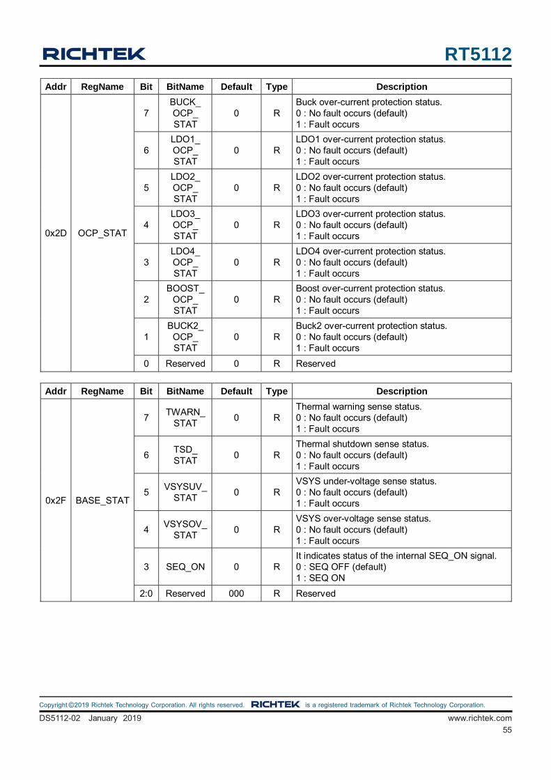
RT5112
55
DS5112-02 January 2019 www.richtek.com
©Copyright 2019 Richtek Technology Corporation. All rights reserved. is a registered trademark of Richtek Technology Corporation.
Addr RegName Bit BitName Default Type Description
0x2D OCP_STAT
7 BUCK_ OCP_ STAT
0 R Buck over-current protection status. 0 : No fault occurs (default) 1 : Fault occurs
6 LDO1_ OCP_ STAT
0 R LDO1 over-current protection status. 0 : No fault occurs (default) 1 : Fault occurs
5 LDO2_ OCP_ STAT
0 R LDO2 over-current protection status. 0 : No fault occurs (default) 1 : Fault occurs
4 LDO3_ OCP_ STAT
0 R LDO3 over-current protection status. 0 : No fault occurs (default) 1 : Fault occurs
3 LDO4_ OCP_ STAT
0 R LDO4 over-current protection status. 0 : No fault occurs (default) 1 : Fault occurs
2 BOOST_
OCP_ STAT
0 R Boost over-current protection status. 0 : No fault occurs (default) 1 : Fault occurs
1 BUCK2_
OCP_ STAT
0 R Buck2 over-current protection status. 0 : No fault occurs (default) 1 : Fault occurs
0 Reserved 0 R Reserved
Addr RegName Bit BitName Default Type Description
0x2F BASE_STAT
7 TWARN_
STAT 0 R
Thermal warning sense status. 0 : No fault occurs (default) 1 : Fault occurs
6 TSD_ STAT
0 R Thermal shutdown sense status. 0 : No fault occurs (default) 1 : Fault occurs
5 VSYSUV_
STAT 0 R
VSYS under-voltage sense status. 0 : No fault occurs (default) 1 : Fault occurs
4 VSYSOV_
STAT 0 R
VSYS over-voltage sense status. 0 : No fault occurs (default) 1 : Fault occurs
3 SEQ_ON 0 R It indicates status of the internal SEQ_ON signal. 0 : SEQ OFF (default) 1 : SEQ ON
2:0 Reserved 000 R Reserved

RT5112
56
DS5112-02 January 2019www.richtek.com
©Copyright 2019 Richtek Technology Corporation. All rights reserved. is a registered trademark of Richtek Technology Corporation.
Addr RegName Bit BitName Default Type Description
0x30 EN_FLG
7 BUCK_EN
_FLG 0 R
Indicate Buck final enable status. 0 : Disable (default) 1 : Enable
6 LDO1_EN
_FLG 0 R
Indicate LDO1 final enable status. 0 : Disable (default) 1 : Enable
5 LDO2_EN
_FLG 0 R
Indicate LDO2 final enable status. 0 : Disable (default) 1 : Enable
4 LDO3_EN
_FLG 0 R
Indicate LDO3 final enable status. 0 : Disable (default) 1 : Enable
3 LDO4_EN
_FLG 0 R
Indicate LDO4 final enable status. 0 : Disable (default) 1 : Enable
2 BOOST_ EN_FLG
0 R Indicate BOOST final enable status. 0 : Disable (default) 1 : Enable
1 BUCK2_ EN_FLG
0 R Indicate Buck2 final enable status. 0 : Disable (default) 1 : Enable
0 Reserved 0 R Reserved

RT5112
57
DS5112-02 January 2019 www.richtek.com
©Copyright 2019 Richtek Technology Corporation. All rights reserved. is a registered trademark of Richtek Technology Corporation.
Addr RegName Bit BitName Default Type Description
0x32 UV_MASK
7 BUCK_UV
_MASK 0 RW
Buck under-voltage threshold mask. 0 : Interrupt is not masked (default) 1 : Interrupt is masked
6 LDO1_UV
_MASK 0 RW
LDO1 under-voltage threshold sense mask. 0 : Interrupt is not masked (default) 1 : Interrupt is masked
5 LDO2_UV
_MASK 0 RW
LDO2 under-voltage threshold sense mask. 0 : Interrupt is not masked (default) 1 : Interrupt is masked
4 LDO3_UV
_MASK 0 RW
LDO3 under-voltage threshold sense mask. 0 : Interrupt is not masked (default) 1 : Interrupt is masked
3 LDO4_UV
_MASK 0 RW
LDO4 under-voltage threshold sense mask. 0 : Interrupt is not masked (default) 1 : Interrupt is masked
2 BOOST_
UV_MASK 0 RW
Boost under-voltage threshold sense mask. 0 : Interrupt is not masked (default) 1 : Interrupt is masked
1 BUCK2_
UV_MASK 0 RW
Buck2 under-voltage threshold sense mask. 0 : Interrupt is not masked (default) 1 : Interrupt is masked
0 BOOST_ FAULT_ MASK
0 RW
Boost SCP (VOUT < 0.7V) or VDS protect (VIN – VOUT > 300mV) or IL > 5A internal boost FAULT mask. 0 : Interrupt is not masked (default) 1 : Interrupt is masked

RT5112
58
DS5112-02 January 2019www.richtek.com
©Copyright 2019 Richtek Technology Corporation. All rights reserved. is a registered trademark of Richtek Technology Corporation.
Addr RegName Bit BitName Default Type Description
0x33 OV_MASK
7 BUCK_
OV_MASK 0 RW
Buck over-voltage threshold mask. 0 : Interrupt is not masked (default) 1 : Interrupt is masked
6 LDO1_OV
_MASK 0 RW
LDO1 over-voltage threshold mask. 0 : Interrupt is not masked (default) 1 : Interrupt is masked
5 LDO2_OV
_MASK 0 RW
LDO2 over-voltage threshold mask. 0 : Interrupt is not masked (default) 1 : Interrupt is masked
4 LDO3_
OV_MASK 0 RW
LDO3 over-voltage threshold mask. 0 : Interrupt is not masked (default) 1 : Interrupt is masked
3 LDO4_
OV_MASK 0 RW
LDO4 over-voltage threshold mask. 0 : Interrupt is not masked (default) 1 : Interrupt is masked
2 BOOST_
OV_MASK 0 RW
Boost over-voltage threshold mask. 0 : Interrupt is not masked (default) 1 : Interrupt is masked
1 BUCK2_
OV_MASK 0 RW
Buck2 over-voltage threshold mask. 0 : Interrupt is not masked (default) 1 : Interrupt is masked
0 Reserved 0 RW Reserved
Addr RegName Bit BitName Default Type Description
0x34 OCP_MASK
7 BUCK_ OCP_ MASK
0 RW Buck over-current protection mask. 0 : Interrupt is not masked (default) 1 : Interrupt is masked
6 LDO1_ OCP_ MASK
0 RW LDO1 over-current protection mask. 0 : Interrupt is not masked (default) 1 : Interrupt is masked
5 LDO2_ OCP_ MASK
0 RW LDO2 over-current protection mask. 0 : Interrupt is not masked (default) 1 : Interrupt is masked
4 LDO3_ OCP_ MASK
0 RW LDO3 over-current protection mask. 0 : Interrupt is not masked (default) 1 : Interrupt is masked
3 LDO4_ OCP_ MASK
0 RW LDO4 over-current protection mask. 0 : Interrupt is not masked (default) 1 : Interrupt is masked
2 BOOST_
OCP_ MASK
0 RW Boost over-current protection mask. 0 : Interrupt is not masked (default) 1 : Interrupt is masked
1 BUCK2_
OCP_ MASK
0 RW Buck2 over-current protection mask. 0 : Interrupt is not masked (default) 1 : Interrupt is masked
0 Reserved 0 RW Reserved

RT5112
59
DS5112-02 January 2019 www.richtek.com
©Copyright 2019 Richtek Technology Corporation. All rights reserved. is a registered trademark of Richtek Technology Corporation.
Addr RegName Bit BitName Default Type Description
0x36 BASE_ MASK
7 TWARN_
MASK 0 RW
Thermal warning sense mask. 0 : Interrupt is not masked (default) 1 : Interrupt is masked
6 TSD_ MASK
0 RW Thermal shutdown sense mask. 0 : Interrupt is not masked (default) 1 : Interrupt is masked
5 VSYSUV_
MASK 0 RW
VSYS under-voltage sense mask. 0 : Interrupt is not masked (default) 1 : Interrupt is masked
4 VSYSOV_
MASK 0 RW
VSYS over-voltage sense mask. 0 : Interrupt is not masked (default) 1 : Interrupt is masked
3:0 Reserved 0000 RW Reserved
Addr RegName Bit BitName Default Type Description
0x37 CHx_PT
7 BUCK_OC_LATCH
0 RW
Buck Hiccup or latch off mode selection after current limit. 0 : Hiccup mode; (Hiccup 3 times will enter latch-off mode. Hiccup on/off time = 4ms / 8ms) (default) 1 : Latch-off mode.
6 LDO_OC_
LATCH 0 RW
LDO Hiccup or latch off mode selection after current limit. 0 : Hiccup mode; (Hiccup 3 times will enter latch-off mode. Hiccup on/off time = 2ms/40ms) (default) 1 : Latch-off mode.
5 BOOST_
OC_ LATCH
0 RW
BOOST Hiccup or latch off mode selection after current limit. 0 : Hiccup mode; (Hiccup 3 times will enter latch-off mode, hiccup on/off time = 10ms/100ms) (default) 1 : Latch-off mode.
4 Reserved 0 RW Reserved
3:2 BST_UV_
DT[1:0] 11 RW
Boost UV deglitch time selection : 00 : 10s 01 : 15s 10 : 25s 11: 50s (default)
1:0 Reserved 00 RW Reserved

RT5112
60
DS5112-02 January 2019www.richtek.com
©Copyright 2019 Richtek Technology Corporation. All rights reserved. is a registered trademark of Richtek Technology Corporation.
Addr RegName Bit BitName Default Type Description
0x38 CHx_deglitch
time
7:6 Buck_UV_
DT[1:0] 11 RW
Buck UV deglitch time selection : 00 : 5s 01 : 10s 10 : 15s 11 : 50s (default)
5:4 Buck_OV_
DT[1:0] 11 RW
Buck OV deglitch time selection : 00 : 10s 01 : 15s 10 : 20s 11 : 50s (default)
3:2 LDO_UV_
DT[1:0] 11 RW
LDO UV deglitch time selection : 00 : 10s 01 : 15s 10 : 30s 11 : 50s (default)
1:0 LDO_OV_
DT[1:0] 11 RW
LDO OV deglitch time selection : 00 : 5s 01 : 10s 10 : 25s 11 : 50s (default)
Addr RegName Bit BitName Default Type Description
0x39 BASEPT_
deglitch time
7:6 VSYSUV_
DT[1:0] 11 RW
VSYSUV deglitch time selection : 00 : 70s 01 : 135s 10 : 265s 11 : 525s (default)
5:4 VSYSOV_
DT[1:0] 10 RW
VSYSOV deglitch time selection: 00 : 20s 01 : 50s 10 : 180s (default) 11 : 360s
3 VSYSOV_
PT 0 RW
VSYSOV turn off Buck 0 : When Vsys_OV occur will turn off BCK (default) 1 : When Vsys_OV occur will not turn off BCK
2 BST_NFC
_Force 0 RW
NFC load detection. 0x05[6] must set 0 when bit BST_NFC_force = 1. 0 : AUTO NFC (default) 1 : FCCM by load, turn off NFC
1 Reserved 0 RW Reserved
0 Reserved 0 RW Reserved

RT5112
61
DS5112-02 January 2019 www.richtek.com
©Copyright 2019 Richtek Technology Corporation. All rights reserved. is a registered trademark of Richtek Technology Corporation.
Addr RegName Bit BitName Default Type Description
0x3A SEQ_ON
7:6 SEQ_ON_STAT[1:0]
00 R
It indicates the states of power on sequence 00 : SEQ_ON hasn't started or needless (default) 01 : SEQ_ON is carrying out (During SLOT1 to SLOT8 + 4ms) 10 : There are fail soft-start channels during power on sequence 11 : SEQ_ON has completed
5:3 SEQ_
COUNT [2:0]
000 R
It indicateds the fault SLOT during power on sequence at SEQ_ON_STAT = 2'b10 000 : SLOT1 (default) 001 : SLOT2 010 : SLOT3 011 : SLOT4 100 : SLOT5 101 : SLOT6 110 : SLOT7 111 : SEQ_ON has completed
2:0 Reserved 000 R Reserved
Addr RegName Bit BitName Default Type Description
0x3B SSEND_CHx
7 sSSEND_
BCK 0 R
It indicates Buck soft-start end or not 0 : Not soft-start end (default) 1 : Soft-start end
6 sSSEND_
LDO1 0 R
It indicates LDO1 soft-start end or not 0 : Not soft-start end (default) 1 : Soft-start end
5 sSSEND_
LDO2 0 R
It indicates LDO2 soft-start end or not 0 : Not soft-start end (default) 1 : Soft-start end
4 sSSEND_
LDO3 0 R
It indicates LDO3 soft-start end or not 0 : Not soft-start end (default) 1 : Soft-start end
3 sSSEND_
LDO4 0 R
It indicates LDO4 soft-start end or not 0 : Not soft-start end (default) 1 : Soft-start end
2 sSSEND_
BST 0 R
It indicates Boost soft-start end or not 0 : Not soft-start end (default) 1 : Soft-start end
1 sSSEND_
BCK2 0 R
It indicates Buck2 soft-start end or not 0 : Not soft-start end (default) 1 : Soft-start end
0 Reserved 0 R Reserved

RT5112
62
DS5112-02 January 2019www.richtek.com
©Copyright 2019 Richtek Technology Corporation. All rights reserved. is a registered trademark of Richtek Technology Corporation.
Addr RegName Bit BitName Default Type Description
0x42 INT_SET
7:6 Reserved 00 RW Reserved
5:4 INT_DEG[
1:0] 00 RW
Interrupt reflash pulse width timing. 00 : disable (default) 01 : 2s 10 : 4s 11 : 8s
3:0 SEQ_STA
T[2:0] 0000 R
Indicate PMU's State 0000 : IDLE (default) 0001 : ONSEQ (slot1 to slot7 + 4ms, when 4ms clock end will tigger ONSEQ_END) 0010 : ONSEQ_END 0011 : ENSEQ 0100 : OFFSEQ 0101 : OFFSEQ_END (slot7 to slot1, when slot1 sequence end will tigger OFFSEQ_END) 1111 : Else
Addr RegName Bit BitName Default Type Description
0x43 PMU_STAT 7:0 PMU_ STAT
00000000 R
BST latch off (BSTEN) 0 : Release (default) 1 : Latch off
BST latch off (HWEN) 0 : Release (default) 1 : Latch off
BCK1 latch off 0 : Release (default) 1 : Latch off
BCK2 latch off 0 : Release (default) 1 : Latch off
LDO1 latch off 0 : Release (default) 1 : Latch off
LDO2 latch off 0 : Release (default) 1 : Latch off
LDO3 latch off 0 : Release (default) 1 : Latch off
LDO4 latch off 0 : Release (default) 1 : Latch off

RT5112
63
DS5112-02 January 2019 www.richtek.com
©Copyright 2019 Richtek Technology Corporation. All rights reserved. is a registered trademark of Richtek Technology Corporation.
0.0
0.5
1.0
1.5
2.0
2.5
3.0
3.5
0 25 50 75 100 125
Ambient Temperature (°C)
Ma
xim
um
Po
we
r D
issi
pa
tion
(W
) 1
Figure 12. Derating Curve of Maximum Power Dissipation
Four-Layer PCBThermal Considerations
The junction temperature should never exceed the
absolute maximum junction temperature TJ(MAX), listed
under Absolute Maximum Ratings, to avoid permanent
damage to the device. The maximum allowable power
dissipation depends on the thermal resistance of the IC
package, the PCB layout, the rate of surrounding airflow,
and the difference between the junction and ambient
temperatures. The maximum power dissipation can be
calculated using the following formula :
PD(MAX) = (TJ(MAX) − TA) / θJA
where TJ(MAX) is the maximum junction temperature, TA is
the ambient temperature, and θJA is the junction-to-ambient
thermal resistance.
For continuous operation, the maximum operating junction
temperature indicated under Recommended Operating
Conditions is 125°C. The junction-to-ambient thermal
resistance, θJA, is highly package dependent. For a WL-
CSP-25B 2.2x2.3 (BSC) package, the thermal resistance,
θJA, is 31.5°C/W on a standard JEDEC 51-7 high effective-
thermal-conductivity four-layer test board. The maximum
power dissipation at TA = 25°C can be calculated as below
:
PD(MAX) = (125°C − 25°C) / (32.7°C/W) = 3.05W for a WL-
CSP-25B 2.2x2.3 (BSC) package.
The maximum power dissipation depends on the operating
ambient temperature for the fixed TJ(MAX) and the thermal
resistance, θJA. The derating curves in Figure 12 allows
the designer to see the effect of rising ambient temperature
on the maximum power dissipation.
Layout Considerations
The PCB layout is an important step to maintain the high
performance of the RT5112. Both the high current and the
fast switching nodes demand full attention to the PCB
layout to keep the robustness of the RT5112 through the
PCB layout. Improper layout might lead to the symptoms
of poor line or load regulation, ground and output voltage
shifts, stability issues, unsatisfying EMI behavior or
worsened efficiency. For the best performance of the
RT5112, the following PCB layout guidelines must be
strictly followed.
The trace from switching node to inductor should be as
short as possible to minimized the switching loop for
better EMI.
Place the input and output capacitors close to the input
and output pins respectively for good filtering.
Keep the main power traces as wide and short as
possible.
Connect the AGND, DGND, GNDB and GNDBST to a
strong ground plane for maximum thermal dissipation
and noise protection.
Directly connect the Buck output capacitors to the
feedback network to avoid bouncing caused by parasitic
resistance and inductance from the PCB trace.
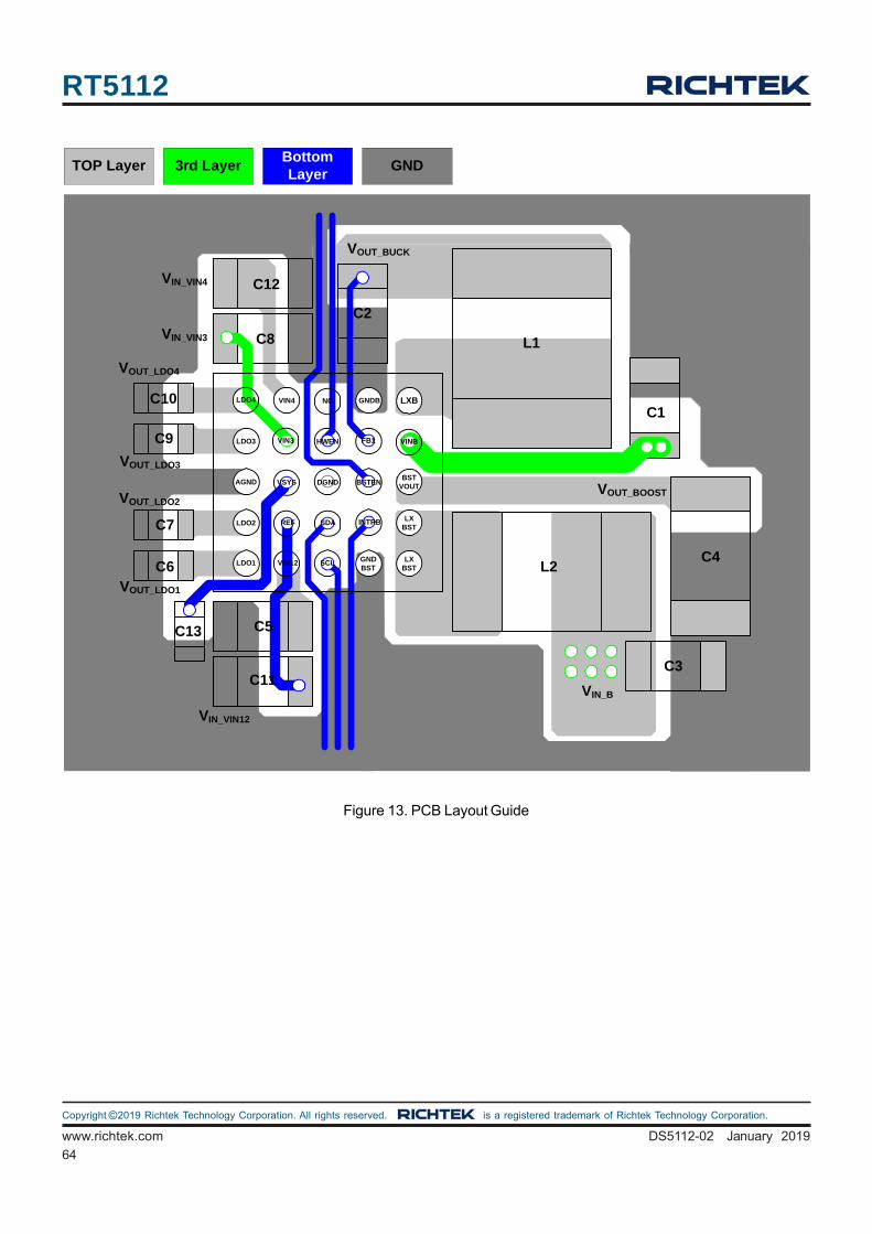
RT5112
64
DS5112-02 January 2019www.richtek.com
©Copyright 2019 Richtek Technology Corporation. All rights reserved. is a registered trademark of Richtek Technology Corporation.
Figure 13. PCB Layout Guide
LXB
BSTVOUT
LXBST
LXBST
GNDB
GNDBST
VIN4
LDO3
AGND
LDO2
LDO1
REF
VIN12
VINB
VSYS
LDO4
VIN3
INTRBSDA
SCL
DGND
NC
TOP Layer 3rd LayerBottom Layer
GND
HWEN
BSTEN
L1
L2
C1
C3
C2
C4
C5
C11
C6
C7
C9
C10
C8
C12
C13
VIN_B
VOUT_BUCK
VOUT_BOOST
VOUT_LDO1
VOUT_LDO3
VOUT_LDO4
VOUT_LDO2
VIN_VIN4
VIN_VIN3
VIN_VIN12
FB1

RT5112
65
DS5112-02 January 2019 www.richtek.com
©Copyright 2019 Richtek Technology Corporation. All rights reserved. is a registered trademark of Richtek Technology Corporation.
Outline Dimension
25B WL-CSP 2.2x2.3 Package (BSC)
Min Max Min Max
A 0.500 0.600 0.020 0.024
A1 0.170 0.230 0.007 0.009
b 0.240 0.300 0.009 0.012
D 2.260 2.340 0.089 0.092
D1
E 2.160 2.240 0.085 0.088
E1
e
1.600 0.063
0.400 0.016
SymbolDimensions In Millimeters Dimensions In Inches
1.600 0.063

RT5112
66
DS5112-02 January 2019www.richtek.com
Richtek Technology Corporation14F, No. 8, Tai Yuen 1st Street, Chupei City
Hsinchu, Taiwan, R.O.C.
Tel: (8863)5526789
Richtek products are sold by description only. Richtek reserves the right to change the circuitry and/or specifications without notice at any time. Customers should
obtain the latest relevant information and data sheets before placing orders and should verify that such information is current and complete. Richtek cannot
assume responsibility for use of any circuitry other than circuitry entirely embodied in a Richtek product. Information furnished by Richtek is believed to be
accurate and reliable. However, no responsibility is assumed by Richtek or its subsidiaries for its use; nor for any infringements of patents or other rights of third
parties which may result from its use. No license is granted by implication or otherwise under any patent or patent rights of Richtek or its subsidiaries.
Footprint Information
e A B
NSMD 0.240 0.340
SMD 0.270 0.240
ToleranceFootprint Dimension (mm)
PackageNumber of
PinType
±0.0250.400WL-CSP2.2x2.3-25(BSC) 25


![Notice for TAIYO YUDEN Products [ For General … for TAIYO YUDEN Products [ For General Electronic Equipment ] Please read this notice before using the TAIYO YUDEN products. REMINDERS](https://img.pdfslide.us/doc/110x75/5c85e46209d3f2700a8b9840/notice-for-taiyo-yuden-products-for-general-for-taiyo-yuden-products-for-general.jpg)


![Notice for TAIYO YUDEN Products (General … for TAIYO YUDEN Products [ For General Electronic Equipment (General Environment) ] Please read this notice before using the TAIYO YUDEN](https://img.pdfslide.us/doc/110x75/5aa4c9217f8b9ac8748c5d02/notice-for-taiyo-yuden-products-general-for-taiyo-yuden-products-for-general.jpg)


![Notice for TAIYO YUDEN Products (General Environment) ]](https://img.pdfslide.us/doc/110x75/61d01fc6eb7c74517f018363/notice-for-taiyo-yuden-products-general-environment-.jpg)