Embed Size (px)
Citation preview

39
Notice for TAIYO YUDEN products Please read this notice before using the TAIYO YUDEN products.
△! 当社カタログをご使用の際には「当社製品に関するお断り」を必ずお読みください。 △! Please read the "Notice for TAIYO YUDEN products" before using this catalog.
1
INFO
RM
ATION
ON
THE G
ENER
AL C
ATALO
G
REMINDERS
■ Product information in this catalog is as of October 2008. All of the contents specified herein are subject to change without notice due to technical improvements, etc. Therefore, please check for the latest information carefully before practical application or usage of the Products.
Please note that Taiyo Yuden Co., Ltd. shall not be responsible for any defects in products or equipment incorporating such products, which are caused under the conditions other than those specified in this catalog or individual specification.
■ Please contact Taiyo Yuden Co., Ltd. for further details of product specifications as the individual specification is available.
■ Please conduct validation and verification of products in actual condition of mounting and operating environment before commercial shipment of the equipment.
■ All electronic components or functional modules listed in this catalog are developed, designed and intended for use in general electronics equipment.(for AV, office automation, household, office supply, information service, telecommunications, (such as mobile phone or PC) etc.). Before incorporating the components or devices into any equipment in the field such as transportation,( automotive control, train control, ship control), transportation signal, disaster prevention, medical, public information network (telephone exchange, base station) etc. which may have direct influence to harm or injure a human body, please contact Taiyo Yuden Co., Ltd. for more detail in advance.
Do not incorporate the products into any equipment in fields such as aerospace, aviation, nuclear control, submarine system, military, etc. where higher safety and reliability are especially required.
In addition, even electronic components or functional modules that are used for the general electronic equipment, if the equipment or the electric circuit require high safety or reliability function or performances, a sufficient reliability evaluation check for safety shall be performed before commercial shipment and moreover, due consideration to install a protective circuit is strongly recommended at customer's design stage.
■ The contents of this catalog are applicable to the products which are purchased from our sales offices or distributors (so called “TAIYO YUDEN’s official sales channel”).
It is only applicable to the products purchased from any of TAIYO YUDEN’ s official sales channel.
■ Please note that Taiyo Yuden Co., Ltd. shall have no responsibility for any controversies or disputes that may occur in connection with a third party's intellectual property rights and other related rights arising from your usage of products in this catalog. Taiyo Yuden Co., Ltd. grants no license for such rights.
■ Caution for export Certain items in this catalog may require specific procedures for export according to “Foreign
Exchange and Foreign Trade Control Law” of Japan, “U.S. Export Administration Regulations”, and other applicable regulations. Should you have any question or inquiry on this matter, please contact our sales staff.
Should you have any question or inquiry on this matter, please contact our sales staff.

特長 FEATURES
形名表記法 ORDERING CODE
用途 APPLICATIONS
76 9△! 当社カタログをご使用の際には「当社製品に関するお断り」を必ずお読みください。 △! Please read the "Notice for TAIYO YUDEN products" before using this catalog.
H 100 Q 250 S 630
・内部電極にNi金属を使用しており、マイグレーションが発生せず、 高信頼性を示す。・高定格電圧でありながら小型形状
中高耐圧積層セラミックコンデンサMEDIUM-HIGH VOLTAGE MULTILAYERCERAMIC CAPACITOR
K ±10% M ±20%
K メッキ品
1定格電圧(VDC)
3 5 7容量許容差
- 標準個別仕様9
8
6公称静電容量(pF)
4 10
当社管理記号11
M 積層コンデンサ
2シリーズ名
例 104 100,000 105 1,000,000
△ 標準品△=スペース
・一般電話交換機・インバータ・無線、通信基地局・DC/DCコンバータ用
端子電極
・The use of Nickel(Ni) as material for internal electrodes almost complete-
ly eliminates migration and high reliability
・Small case sizes with high rated voltage
・General telephone exchange
・Inverter.
・Wireless and Telecommunication base.
・For DC/DC Converter
107(0603) 1.6×0.8 212(0805) 2.0×1.25 316(1206) 3.2×1.6 325(1210) 3.2×2.5 432(1812) 4.5×3.2
形状寸法(EIA)L×W(mm)
A 0.8 D 0.85 G 1.25 F 1.15 L 1.6 N 1.9 M 2.5
製品厚み(mm)
H M K 3 1 6 B J 1 0 4 K L _ T △6 7 854321 9 10 11
H 100 Q 250 S 630
K ±10% M ±20%
K Plated
1Rated voltage(VDC)
3End termination
5 7Capacitance tolerance
- Standard products
9
84 10
11Internal code
M
Multilayer ceramic capacitors
2 Series name
Special code
△ Standard products
6Nominal capacitance(pF)
example 104 100,000 105 1,000,000
△=Blank space
107(0603) 1.6×0.8 212(0805) 2.0×1.25 316(1206) 3.2×1.6 325(1210) 3.2×2.5 432(1812) 4.5×3.2
Dimensions(case size)(mm)Thickness(mm)
A 0.8 D 0.85 G 1.25 F 1.15 L 1.6 N 1.9 M 2.5
Code Temp.characteristics Operating temp. range
OPERATING TEMP.BJ
B -25~+85℃X5R* -55~+85℃
B7 X7R -55~+125℃C7 X7S -55~+125℃
*個別仕様の取交しにより、X7R/X7S仕様に対応している場合があります。*We may provide X7R/X7S for some items according to the individual
specification.
温度特性BJ
BX5R
B7 X7RC7 X7S
Temperature characteristics code
BJB
X5RB7 X7RC7 X7S
T
φ178mm テーピング (4mmピッチ)
包装
T
φ178mm Taping (4mm pitch)
Packaging

外形寸法 EXTERNAL DIMENSIONS
779
CA
PAC
ITOR
S
4
△! 当社カタログをご使用の際には「当社製品に関するお断り」を必ずお読みください。 △! Please read the "Notice for TAIYO YUDEN products" before using this catalog.
概略バリエーション AVAILABLE CAPACITANCE RANGE
※グラフ記号は製品厚みを表します。 Letters in the table indicate thickness.
Type(EIA) L W T e
L
□MK316(1206)
3.2±0.15(0.126±0.006)
1.6±0.15(0.063±0.006) 1.6±0.20
(0.063±0.008)
F1.15±0.10
(0.045±0.004)
F1.15±0.10
(0.045±0.004)□MK325(1210)
3.2±0.3(0.126±0.012)
2.5±0.20(0.098±0.008)
N1.9±0.20
(0.075±0.008)
M□MK432(1812)
4.5±0.4(0.177±0.016)
3.2±0.30(0.126±0.012)
2.5±0.20(0.098±0.008)
D□MK212(0805)
2.0±0.10(0.079±0.004)
1.25±0.10(0.049±0.004)
0.85±0.10(0.033±0.004)
G1.25±0.10
(0.049±0.004)
0.5±0.25(0.020±0.010)
0.6±0.3(0.024±0.012)
0.9±0.6(0.035±0.024)
0.5+0.35-0.25
(0.020+0.014ー0.010)
A□MK107(0603)
1.6±0.10(0.063±0.004)
0.8±0.10(0.031±0.004)
0.8±0.10(0.031±0.004)
0.35±0.25(0.014±0.010)
Unit:mm(inch)
P.78 P.83 P.98 P.84 P.108P.12
アイテム一覧Part Numbers
特性図Electrical Characteristics
梱包Packaging
信頼性Reliability Data
使用上の注意Precautions
セレクションガイドSelection Guide
etc
*: 代表的な値を記載しています。詳細はアイテム一覧表を参照ください。*: The figure indicates typical value. Please refer to PART NUMBERS table.
温度特性コードTemp.char.Code
温度特性Temperature characteristics 静電容量許容差〔%〕
Capacitance tolerancetanδ〔%〕
Dissipation factor準拠規格Applicable standard
温度範囲〔℃〕Temperature range
基準温度〔℃〕Ref. Temp.
静電容量変化率〔%〕Capacitance change
BJJIS B -25~+85 20 ±10
±10(K)±20(M) 2.5 max.*
EIA X5R -55~+85 25 ±15B7 EIA X7R -55~+125 25 ±15C7 EIA X7S -55~+125 25 ±22
Cap[μF]
Type 107 212 316 325 432Temp.Char
X7R X7S B/X5R X7R B/X5R X7R B/X5R X7R B/X5R X7R B/X5R
VDC 100V 100V 100V 100V 250V 100V 250V 100V 250V 630V 100V 250V 630V 100V 250V 630V 100V 250V 630V 100V 250V 630V 100V 250V 630V[pF:3digits]
0.001 102 A A D D F F0.0015 152 A A D D F F0.0022 222 A A D D F F0.0033 332 A A D D F F0.0047 472 A A G G F F0.0068 682 A A G G F F0.01 103 A A G G G G F F0.015 153 A A G G G G L L0.022 223 A A G G G G L L N N0.033 333 A A G G L L N N0.047 473 G G L L L L N N N N M M0.068 683 G G L L M M0.1 104 A A G G L L L L F N F N M M M M0.15 154 L L N N0.22 224 G G L L N N N N M M0.33 334 L L M M0.47 474 L L N N M M M M0.68 684 N N1.0 105 L L N N M M1.5 155 M M
2.2 225 N N M M

78 9
アイテム一覧 PART NUMBERS
△! 当社カタログをご使用の際には「当社製品に関するお断り」を必ずお読みください。 △! Please read the "Notice for TAIYO YUDEN products" before using this catalog.
■ 107TYPE(0603 case size)【温度特性 Temp.char. BJ:B/X5R】
定格電圧Rated Voltage
形 名Ordering code
EHS(Environmental
HazardousSubstances)
公 称静電容量
Capacitance〔μF〕
温度特性Temperature
characteristics
tanδDissipation
factor〔%〕Max.
実装条件Soldering method
R:リフロー Reflow soldering
W: フロー Wave soldering
静電容量許 容 差
Capacitancetolerance
厚 みThickness〔mm〕(inch)
100V
HMK107 BJ102□A RoHS 0.001
B/X5R*2 3.5 R±10%±20%
0.8±0.1(0.031±0.0041)
HMK107 BJ152□A RoHS 0.0015HMK107 BJ222□A RoHS 0.0022HMK107 BJ332□A RoHS 0.0033HMK107 BJ472□A RoHS 0.0047HMK107 BJ682□A RoHS 0.0068HMK107 BJ103□A RoHS 0.01HMK107 BJ153□A RoHS 0.015HMK107 BJ223□A RoHS 0.022HMK107 BJ333□A RoHS 0.033HMK107 BJ104□A RoHS 0.1
形名の□には静電容量許容差記号が入ります。*2 個別仕様の取交しにより、X7R/X7S仕様に対応している場合があります。
【温度特性 Temp.char. B7:X7R C7:X7S】
定格電圧Rated Voltage
形 名Ordering code
EHS(Environmental
HazardousSubstances)
公 称静電容量
Capacitance〔μF〕
温度特性Temperature
characteristics
tanδDissipation
factor〔%〕Max.
実装条件Soldering method
R:リフロー Reflow soldering
W: フロー Wave soldering
静電容量許 容 差
Capacitancetolerance
厚 みThickness〔mm〕(inch)
100V
HMK107 B7 102□A RoHS 0.001
X7R3.5 R
±10%±20%
0.8±0.1(0.031±0.0041)
HMK107 B7 152□A RoHS 0.0015HMK107 B7 222□A RoHS 0.0022HMK107 B7 332□A RoHS 0.0033HMK107 B7 472□A RoHS 0.0047HMK107 B7 682□A RoHS 0.0068HMK107 B7 103□A RoHS 0.01HMK107 B7 153□A RoHS 0.015HMK107 B7 223□A RoHS 0.022HMK107 B7 333□A RoHS 0.033HMK107 C7 104□A RoHS 0.1 X7S
□ Please specify the capacitance tolerance code.形名の□には静電容量許容差記号が入ります。
□ Please specify the capacitance tolerance code.*2 We may provide X7R/X7S for some items according to the individual
specification.

CA
PAC
ITOR
S
4
799
アイテム一覧 PART NUMBERS
△! 当社カタログをご使用の際には「当社製品に関するお断り」を必ずお読みください。 △! Please read the "Notice for TAIYO YUDEN products" before using this catalog.
■ 212TYPE(0805 case size)【温度特性 Temp.char. BJ:B/X5R】
定格電圧Rated Voltage
形 名Ordering code
EHS(Environmental
HazardousSubstances)
公 称静電容量
Capacitance〔μF〕
温度特性Temperature
characteristics
tanδDissipation
factor〔%〕Max.
実装条件Soldering method
R:リフロー Reflow soldering
W: フロー Wave soldering
静電容量許 容 差
Capacitancetolerance
厚 みThickness〔mm〕(inch)
100V
HMK212 BJ103□G RoHS 0.01
B/X5R*2
3.5
R±10%±20%
1.25±0.1(0.049±0.004)
HMK212 BJ153□G RoHS 0.015HMK212 BJ223□G RoHS 0.022HMK212 BJ333□G RoHS 0.033HMK212 BJ473□G RoHS 0.047HMK212 BJ683□G RoHS 0.068HMK212 BJ104□G RoHS 0.1HMK212 BJ224□G RoHS 0.22
250V
QMK212 BJ102□D RoHS 0.001
2.5
0.85±0.1(0.033±0.004)
QMK212 BJ152□D RoHS 0.0015QMK212 BJ222□D RoHS 0.0022QMK212 BJ332□D RoHS 0.0033QMK212 BJ472□G RoHS 0.0047
1.25±0.1(0.049±0.004)
QMK212 BJ682□G RoHS 0.0068QMK212 BJ103□G RoHS 0.01QMK212 BJ153□G RoHS 0.015QMK212 BJ223□G RoHS 0.022
【温度特性 Temp.char. B7:X7R】
定格電圧Rated Voltage
形 名Ordering code
EHS(Environmental
HazardousSubstances)
公 称静電容量
Capacitance〔μF〕
温度特性Temperature
characteristics
tanδDissipation
factor〔%〕Max.
実装条件Soldering method
R:リフロー Reflow soldering
W: フロー Wave soldering
静電容量許 容 差
Capacitancetolerance
厚 みThickness〔mm〕(inch)
100V
HMK212 B7 103□G RoHS 0.01
X7R
3.5
R±10%±20%
1.25±0.1(0.049±0.004)
HMK212 B7 153□G RoHS 0.015HMK212 B7 223□G RoHS 0.022HMK212 B7 333□G RoHS 0.033HMK212 B7 473□G RoHS 0.047HMK212 B7 683□G RoHS 0.068HMK212 B7 104□G RoHS 0.1HMK212 B7 224□G RoHS 0.22
250V
QMK212 B7 102□D RoHS 0.001
2.5
0.85±0.1(0.033±0.004)
QMK212 B7 152□D RoHS 0.0015QMK212 B7 222□D RoHS 0.0022QMK212 B7 332□D RoHS 0.0033QMK212 B7 472□G RoHS 0.0047
1.25±0.1(0.049±0.004)
QMK212 B7 682□G RoHS 0.0068QMK212 B7 103□G RoHS 0.01QMK212 B7 153□G RoHS 0.015QMK212 B7 223□G RoHS 0.022
□ Please specify the capacitance tolerance code.形名の□には静電容量許容差記号が入ります。
形名の□には静電容量許容差記号が入ります。*2 個別仕様の取交しにより、X7R仕様に対応している場合があります。
□ Please specify the capacitance tolerance code.*2 We may provide X7R for some items according to the individual specifi-
cation.

80 9
アイテム一覧 PART NUMBERS
△! 当社カタログをご使用の際には「当社製品に関するお断り」を必ずお読みください。 △! Please read the "Notice for TAIYO YUDEN products" before using this catalog.
■ 316TYPE(1206 case size)【温度特性 Temp.char. BJ:B/X5R】
定格電圧Rated Voltage
形 名Ordering code
EHS(Environmental
HazardousSubstances)
公 称静電容量
Capacitance〔μF〕
温度特性Temperature
characteristics
tanδDissipation
factor〔%〕Max.
実装条件Soldering method
R:リフロー Reflow soldering
W: フロー Wave soldering
静電容量許 容 差
Capacitancetolerance
厚 みThickness〔mm〕(inch)
100V
HMK316 BJ473□L RoHS 0.047
B/X5R*2
3.5
R±10%±20%
1.6±0.2(0.063±0.008)
HMK316 BJ104□L RoHS 0.1HMK316 BJ154□L RoHS 0.15HMK316 BJ224□L RoHS 0.22HMK316 BJ334□L RoHS 0.33HMK316 BJ474□L RoHS 0.47HMK316 BJ105□L RoHS 1
250V
QMK316 BJ333□L RoHS 0.033
2.5
QMK316 BJ473□L RoHS 0.047QMK316 BJ683□L RoHS 0.068QMK316 BJ104□L RoHS 0.1
630V
SMK316 BJ102□F RoHS 0.001
1.15±0.1(0.045±0.004)
SMK316 BJ152□F RoHS 0.0015SMK316 BJ222□F RoHS 0.0022SMK316 BJ332□F RoHS 0.0033SMK316 BJ472□F RoHS 0.0047SMK316 BJ682□F RoHS 0.0068SMK316 BJ103□F RoHS 0.01SMK316 BJ153□L RoHS 0.015 1.6±0.2
(0.063±0.008)SMK316 BJ223□L RoHS 0.022
□ Please specify the capacitance tolerance code.形名の□には静電容量許容差記号が入ります。
【温度特性 Temp.char. B7:X7R】
定格電圧Rated Voltage
形 名Ordering code
EHS(Environmental
HazardousSubstances)
公 称静電容量
Capacitance〔μF〕
温度特性Temperature
characteristics
tanδDissipation
factor〔%〕Max.
実装条件Soldering method
R:リフロー Reflow soldering
W: フロー Wave soldering
静電容量許 容 差
Capacitancetolerance
厚 みThickness〔mm〕(inch)
100V
HMK316 B7 473□L RoHS 0.047
X7R
3.5
R±10%±20%
1.6±0.2(0.063±0.008)
HMK316 B7 104□L RoHS 0.1HMK316 B7 154□L RoHS 0.15HMK316 B7 224□L RoHS 0.22HMK316 B7 334□L RoHS 0.33HMK316 B7 474□L RoHS 0.47HMK316 B7 105□L RoHS 1
250V
QMK316 B7 333□L RoHS 0.033
2.5
QMK316 B7 473□L RoHS 0.047QMK316 B7 683□L RoHS 0.068QMK316 B7 104□L RoHS 0.1
630V
SMK316 B7 102□F RoHS 0.001
1.15±0.1(0.045±0.004)
SMK316 B7 152□F RoHS 0.0015SMK316 B7 222□F RoHS 0.0022SMK316 B7 332□F RoHS 0.0033SMK316 B7 472□F RoHS 0.0047SMK316 B7 682□F RoHS 0.0068SMK316 B7 103□F RoHS 0.01SMK316 B7 153□L RoHS 0.015 1.6±0.2
(0.063±0.008)SMK316 B7 223□L RoHS 0.022
形名の□には静電容量許容差記号が入ります。*2 個別仕様の取交しにより、X7R仕様に対応している場合があります。
□ Please specify the capacitance tolerance code.*2 We may provide X7R for some items according to the individual specifi-
cation.
CA
PAC
ITOR
S
4
819
アイテム一覧 PART NUMBERS
△! 当社カタログをご使用の際には「当社製品に関するお断り」を必ずお読みください。 △! Please read the "Notice for TAIYO YUDEN products" before using this catalog.
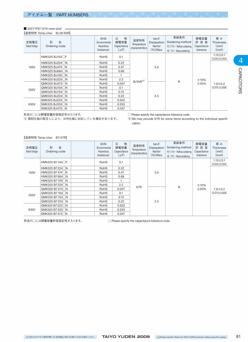
【温度特性 Temp.char. B7:X7R】
定格電圧Rated Voltage
形 名Ordering code
EHS(Environmental
HazardousSubstances)
公 称静電容量
Capacitance〔μF〕
温度特性Temperature
characteristics
tanδDissipation
factor〔%〕Max.
実装条件Soldering method
R:リフロー Reflow soldering
W: フロー Wave soldering
静電容量許 容 差
Capacitancetolerance
厚 みThickness〔mm〕(inch)
100V
HMK325 B7 104□F RoHS 0.1
X7R
3.5
R±10%±20%
1.15±0.1(0.045±0.004)
HMK325 B7 224□N RoHS 0.22
1.9±0.2(0.075±0.008)
HMK325 B7 474□N RoHS 0.47HMK325 B7 684□N RoHS 0.68HMK325 B7 105□N RoHS 1HMK325 B7 225□N RoHS 2.2
250V
QMK325 B7 473□N RoHS 0.047
2.5
QMK325 B7 104□N RoHS 0.1QMK325 B7 154□N RoHS 0.15QMK325 B7 224□N RoHS 0.22
630VSMK325 B7 223□N RoHS 0.022SMK325 B7 333□N RoHS 0.033SMK325 B7 473□N RoHS 0.047
□ Please specify the capacitance tolerance code.形名の□には静電容量許容差記号が入ります。
■ 325TYPE(1210 case size)【温度特性 Temp.char. BJ:B/X5R】
定格電圧Rated Voltage
形 名Ordering code
EHS(Environmental
HazardousSubstances)
公 称静電容量
Capacitance〔μF〕
温度特性Temperature
characteristics
tanδDissipation
factor〔%〕Max.
実装条件Soldering method
R:リフロー Reflow soldering
W: フロー Wave soldering
静電容量許 容 差
Capacitancetolerance
厚 みThickness〔mm〕(inch)
100V
HMK325 BJ104□F RoHS 0.1
B/X5R*2
3.5
R±10%±20%
1.15±0.1(0.045±0.004)
HMK325 BJ224□N RoHS 0.22
1.9±0.2(0.075±0.008)
HMK325 BJ474□N RoHS 0.47HMK325 BJ684□N RoHS 0.68HMK325 BJ105□N RoHS 1HMK325 BJ225□N RoHS 2.2
250V
QMK325 BJ473□N RoHS 0.047
2.5
QMK325 BJ104□N RoHS 0.1QMK325 BJ154□N RoHS 0.15QMK325 BJ224□N RoHS 0.22
630VSMK325 BJ223□N RoHS 0.022SMK325 BJ333□N RoHS 0.033SMK325 BJ473□N RoHS 0.047
形名の□には静電容量許容差記号が入ります。*2 個別仕様の取交しにより、X7R仕様に対応している場合があります。
□ Please specify the capacitance tolerance code.*2 We may provide X7R for some items according to the individual specifi-
cation.

82 9
アイテム一覧 PART NUMBERS
△! 当社カタログをご使用の際には「当社製品に関するお断り」を必ずお読みください。 △! Please read the "Notice for TAIYO YUDEN products" before using this catalog.
■ 432TYPE(1812 case size)【温度特性 Temp.char. BJ:B/X5R】
定格電圧Rated Voltage
形 名Ordering code
EHS(Environmental
HazardousSubstances)
公 称静電容量
Capacitance〔μF〕
温度特性Temperature
characteristics
tanδDissipation
factor〔%〕Max.
実装条件Soldering method
R:リフロー Reflow soldering
W: フロー Wave soldering
静電容量許 容 差
Capacitancetolerance
厚 みThickness〔mm〕(inch)
100V
HMK432 BJ474□M RoHS 0.47
B/X5R*2
3.5
R±10%±20%
2.5±0.2(0.098±0.008)
HMK432 BJ105□M RoHS 1HMK432 BJ155□M RoHS 1.5HMK432 BJ225□M RoHS 2.2
250V
QMK432 BJ104□M RoHS 0.1
2.5
QMK432 BJ224□M RoHS 0.22QMK432 BJ334□M RoHS 0.33QMK432 BJ474□M RoHS 0.47
630VSMK432 BJ473□M RoHS 0.047SMK432 BJ683□M RoHS 0.068SMK432 BJ104□M RoHS 0.1
【温度特性 Temp.char. B7:X7R】
定格電圧Rated Voltage
形 名Ordering code
EHS(Environmental
HazardousSubstances)
公 称静電容量
Capacitance〔μF〕
温度特性Temperature
characteristics
tanδDissipation
factor〔%〕Max.
実装条件Soldering method
R:リフロー Reflow soldering
W: フロー Wave soldering
静電容量許 容 差
Capacitancetolerance
厚 みThickness〔mm〕(inch)
100V
HMK432 B7 474□M RoHS 0.47
X7R
3.5
R±10%±20%
2.5±0.2(0.098±0.008)
HMK432 B7 105□M RoHS 1HMK432 B7 155□M RoHS 1.5HMK432 B7 225□M RoHS 2.2
250V
QMK432 B7 104□M RoHS 0.1
2.5
QMK432 B7 224□M RoHS 0.22QMK432 B7 334□M RoHS 0.33QMK432 B7 474□M RoHS 0.47
630VSMK432 B7 473□M RoHS 0.047SMK432 B7 683□M RoHS 0.068SMK432 B7 104□M RoHS 0.1
□ Please specify the capacitance tolerance code.形名の□には静電容量許容差記号が入ります。
形名の□には静電容量許容差記号が入ります。*2 個別仕様の取交しにより、X7R仕様に対応している場合があります。
□ Please specify the capacitance tolerance code.*2 We may provide X7R for some items according to the individual specifi-
cation.
CA
PAC
ITOR
S
4
839△! 当社カタログをご使用の際には「当社製品に関するお断り」を必ずお読みください。 △! Please read the "Notice for TAIYO YUDEN products" before using this catalog.
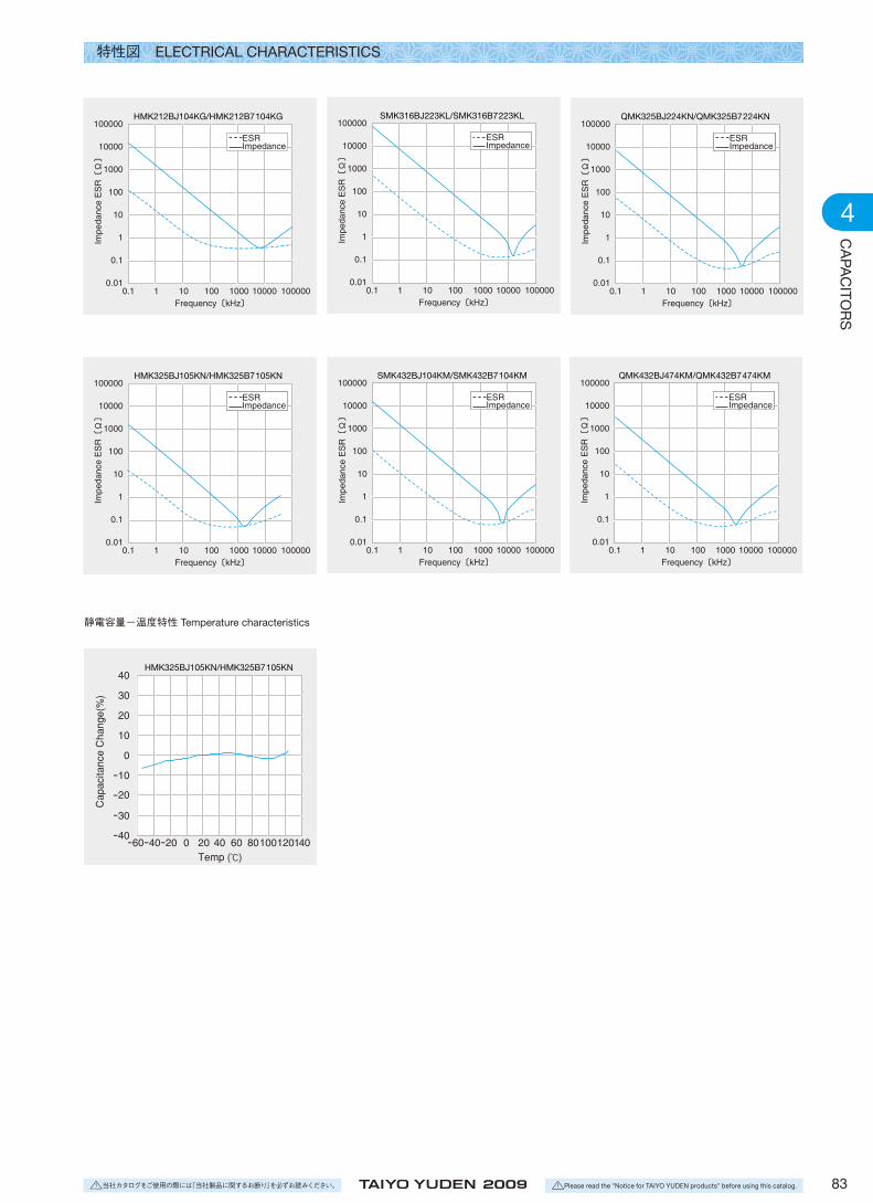
静電容量-温度特性 Temperature characteristics
HMK212BJ104KG/HMK212B7104KG
HMK325BJ105KN/HMK325B7105KN
QMK325BJ224KN/QMK325B7224KN
QMK432BJ474KM/QMK432B7474KM
SMK316BJ223KL/SMK316B7223KL
SMK432BJ104KM/SMK432B7104KM
HMK325BJ105KN/HMK325B7105KN
特性図 ELECTRICAL CHARACTERISTICS

98 △! 当社カタログをご使用の際には「当社製品に関するお断り」を必ずお読みください。 △! Please read the "Notice for TAIYO YUDEN products" before using this catalog.
C0.2(0.008)0.3(0.012)0.3(0.012)0.45(0.018)0.3(0.012)
0.5(0.020)
0.5(0.020)0.8(0.031)
0.8(0.031)0.5(0.020)
0.6(0.024)0.45(0.018)0.85(0.033)1.25(0.049)0.85(0.033)0.85(0.033)0.85(0.033)1.15(0.045)1.25(0.049)1.6(0.063)
0.85(0.033)1.15(0.045)1.5(0.059)1.9(0.075)
2.0max(0.079)
2.5(0.098)
2.5(0.098)
■テーピング梱包 Taped packaging
P
P
P
K
V, W
W
□MK063(0201)
□
□WK105(0204)
2K096(0302)
□MK042(01005)
□MK105(0402)□VK105(0402)
mm(inch) code
製品厚みThickness形式(EIA)
Type
15000
15000
10000
10000
10000
標準数量Standard quantity
[ pcs ]紙テープ
paperエンボステープEmbossed tape
A
B
A
K
D
G
D
D
D
F
G
L
D
F
H
N
Y
M
□WK107(0306)□MK107(0603)
□2K110(0504)
□MK212(0805)□WK212(0508)
□4K212(0805)□2K212(0805)
□MK316(1206)
□MK325(1210)
□MK432(1812)
3000
3000
2000
2000
2000
500
500(T),1000(P)
V
V
4000
0.45(0.018) 4000K
4000
4000 4000 4000 4000
4000
4000
4000
4000
M
梱包 PACKAGING
②テーピング材質 Taping material
※□WK
※□WK
Unit:mm (inch)105, 107, 212形状で個別対応致しますのでお問い合せ下さい。Please contact any of our offices for accepting your requirement accord-ing to dimensions 0402, 0603, 0805.(inch)
③バルクカセット Bulk Cassette
①最小受注単位数 Minimum Quantity
※プレスポケットタイプは、 ボトムテープ無し。
CA
PAC
ITOR
S
4
99△! 当社カタログをご使用の際には「当社製品に関するお断り」を必ずお読みください。 △! Please read the "Notice for TAIYO YUDEN products" before using this catalog.
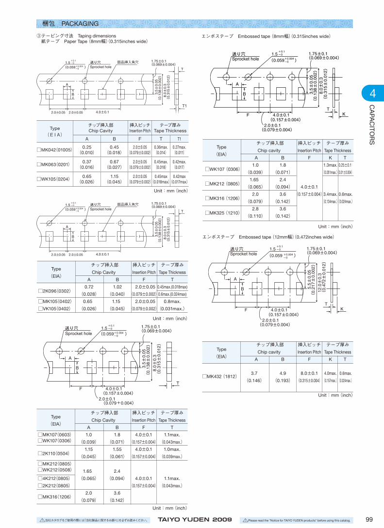
梱包 PACKAGING
③テーピング寸法 Taping dimensions 紙テープ Paper Tape(8mm幅)(0.315inches wide)
2.0±0.052.0±0.05
T1
部品挿入角穴
Unit:mm(inch)
Unit:mm(inch)
Type
チップ挿入部 挿入ピッチ テープ厚み
(EIA) Chip cavity Insertion Pitch Tape Thickness
A B F K T
3.7
4.9
8.0±0.1
0.6max.□MK432(1812)
(0.146)
(0.193)
(0.315±0.004) 4.0max.
(0.024max.) (0.157max.)
エンボステープ Embossed tape(8mm幅)(0.315inches wide)
Unit:mm(inch)
エンボステープ Embossed tape(12mm幅)(0.472inches wide)
Type
チップ挿入部 挿入ピッチ テープ厚み
(EIA) Chip Cavity Insertion Pitch Tape Thickness
A B F T
□MK107(0603) 1.0 1.8 4.0±0.1 1.1max.
□WK107(0306) (0.039) (0.071) (0.157±0.004) (0.043max.)
□2K110(0504) 1.15 1.55 4.0±0.1 1.0max.
(0.045) (0.061) (0.157±0.004) (0.039max.)
□MK212(0805)
□WK212(0508) 1.655 2.4
□4K212(0805) (0.065) (0.094) 4.0±0.1 1.1max.
□2K212(0805) (0.157±0.004) (0.043max.)
□MK316(1206) 2.0 3.6
(0.079) (0.142)
Unit:mm(inch)
Type
チップ挿入部 挿入ピッチ テープ厚み
(EIA) Chip Cavity Insertion Pitch Tape Thickness
A B F T
□2K096(0302) 0.72 1.02 52.0±0.05 0.45max.(0.018max)
(0.028) (0.040) (0.079±0.002) 0.6max.(0.024max)
□MK105(0402) 0.655 1.155 52.0±0.05 0.8max.
□VK105(0402) (0.026) (0.045) (0.079±0.002) (0.031max.)
2.0±0.052.0±0.05
部品挿入角穴
Type
チップ挿入部 挿入ピッチ テープ厚み
(EIA) Chip cavity Insertion Pitch Tape Thickness
A B F K T
□WK107(0306) 1.0 1.8 1.3max. 0.25±0.1
(0.039) (0.071) (0.051max.) (0.01±0.004)
□MK212(0805) 1.655 2.4
(0.065) (0.094) 4.0±0.1
□MK316(1206) 2.0 3.6 (0.157±0.004) 3.4max. 0.6max.
(0.079) (0.142) (0.134max.) (0.024max.)
□MK325(1210) 2.8 3.6
(0.110) (0.142)
Type(EIA)
チップ挿入部Chip Cavity
挿入ピッチInsertion Pitch
テープ厚みTape Thickness
A B F T T1
□MK042(01005) 0.25(0.010)
0.45(0.018)
2.0±0.05(0.079±0.002)
0.36max.(0.014)
0.27max.(0.011)
□MK063(0201) 0.37(0.016)
0.67(0.027)
2.0±0.05(0.079±0.002)
0.45max.(0.018)
0.42max.(0.017)
□WK105(0204) 0.65(0.026)
1.15(0.045)
2.0±0.05(0.079±0.002)
0.45max(0.018max)
0.42max(0.017max)
Unit:mm(inch)

100 △! 当社カタログをご使用の際には「当社製品に関するお断り」を必ずお読みください。 △! Please read the "Notice for TAIYO YUDEN products" before using this catalog.
④リーダー部/空部 Leader and Blank portion
160mm以上(6.3inches or more)
引き出し方向Direction of tape feed
100mm以上(3.94inches or more)
400mm以上(15.7inches or more)
⑤リール寸法 Reel size
⑥トップテープ強度 Top Tape Strength
トップテープのはがし力は下図矢印方向にて0.1~0.7Nとなります。The top tape requires a peel-off force of 0.1~0.7N in the direction of the arrow as illustrated below.
梱包 PACKAGING

CA
PAC
ITOR
S
4
859△! 当社カタログをご使用の際には「当社製品に関するお断り」を必ずお読みください。 △! Please read the "Notice for TAIYO YUDEN products" before using this catalog.
RELIABILITY DATA 1/2
Item Specified Value Test Methods and Remarks
X7R, X7S:ー55 to +125℃ B: ー25 to +85℃
X7R, X7S :ー55 to +125℃ B: ー25 to +85℃
100VDC, 250VDC, 630VDC
No breakdown or damage
100MΩμF or 10GΩ, whichever is smaller.
±20%、±10%
3.5%max(100V).
2.5%max(250V, 630V).
B: ±10%(ー25 to +85℃)
X7R: ±15%(ー55 to +125℃)
X7S: ±22%(-55 to +125℃)
Appearance:No abnormality Capacitance change:Within±10%
No separation or indication of separation of electrode
At least 75% of terminal electrode is covered by solder
Appearance:No abnormality
Capacitance change:Within±15%(100V), ±10%(250V, 630V)
tanδ: Initial value
Insulation resistance:Intial value
Withstanding voltage(between terminals): No abnormality
Appearance:No abnormality
Capacitance change:Within±15%(100V), ±7.5%(250V, 630V)
tanδ: Initial value
Insulation resistance:Initial value
MEDIUMーHIGH VOLTAGE MULTILAYER CERAMIC CAPACITOR
1.Operating Temperature Range
2.Storage Temperature Range
3.Rated Voltage
4.Withstanding Voltage
Between terminals
5.Insulation Resistance
6.Capacitance(Tolerance)
7.Tangent of Loss Angel
8.Temperature Characteristic
of Capacitance
9.Resistance to Flexure of
Substrate
10.Adhesion of Electrode
11.Solderability
12.Resistance to Soldering
13.Thermal shock
Applied voltage:Rated voltage×2.5(100V) Rated voltage×2(250V) Rated voltage×1.2(630V)
Duration:1~5sec.
Chage/dischage current:50mAmax.
Applied voltage:Rated voltage(100V, 250V) 500V(630V)
Duration:60±5sec.
Chage/dischage current:50mAmax.
Measuring frequency:1kHz±10%
Measuring voltage:1±0.2Vrms
Bias application:None
Measuring frequency:1kHz±10%
Measuring voltage:1±0.2Vrms
Bias application:None
According to JIS 5102 clause7.12.
Charge of maximum capacitance deviation in step 1 to 5
Temperature at step 1:+25℃
Temperature at step 2:minimum operating temperature
Temperature at step 3:+25℃(Reference temperature)
Temperature at step 4:maximum operating temperature
Temperature at step 5:+25℃
Reference temperature Characteristic B shall be +20℃
Warp:1mm
Testing boade:glass epoxyーresin substrate
Thickness:1.6mm
The measurement shall be made with board in the bent
position
Applied force:5N
Duration:30±5sec.
Solder temperature:230±5℃
Duration:4±1sec.
Preconditioning:Thermal treatment(at 150℃ for 1hr)
Solder temperature:270±5℃
Duration:3±0.5sec.
Preheating conditions: 80 to 100℃, 2 to 5 min.
150 to 200℃, 2 to 5min.
Recovery:Rcovery for the following reriod under the
standerd condition after the test.
24±2hrs
Preconditioning:Thermal treatment(at 150℃ for 1hr)
Conditions for 1 cycle
Step 1:Minimum operating temperature +0/-3℃ 30±3min.
Step 2:Room temperature 2 to 3min.
Step 3:Maximum operating temperature +0/-3℃ 30±3min.
Step4:Room temperature 2 to 3min.
Number of cycles:5 times
Recovery after the test:24±2hrs
R-230

CA
PAC
ITOR
S
4
879△! 当社カタログをご使用の際には「当社製品に関するお断り」を必ずお読みください。 △! Please read the "Notice for TAIYO YUDEN products" before using this catalog.
RELIABILITY DATA 2/2
Appearance:No abnormality
Capacitance change: Within±15%
tanδ: 7%max(100V), 5%max(250V, 630V).
Insulation resistance:25MΩμF or 1000MΩ Whichever is smaller.
Appearance:No abnormality
Capacitance change: Within±15%
tanδ: 7%max(100V), 5%max(250V, 630V).
Insulation resistance:10MΩμF or 500MΩ Whichever is smaller.
Appearance:No abnormality
Capacitance change: Within±15%
tanδ: 7%max(100V), 5%max(250V, 630V).
Insulation resistance:50MΩμF or 1000MΩ Whichever is smaller.
14.Damp Heat(steady state)
15.Loading under
Damp Heat
16.Loading at High
Temperature
Preconditioning:Thermal treatment(at 150℃ for 1hr)
Temperature:40±2℃
Humidity:90 to 95%RH
Duration: 500+24/ー0 hrs
Recovery:Rcovery for the following reriod under the
standerd condition after the removal from test chamber.
24±2hrs
Preconditioning:Thermal treatment(at 150℃ for 1hr)
Preconditioning:Voltage treatment
Temperature:40±2℃
Humidity:90 to 95%RH
Applied voltage:Rated voltage
Chage/dischage current:50mAmax.
Duration: 500+24/ー0 hrs
Recovery:Rcovery for the following reriod under the
standerd condition after the removal from test chamber.
24±2hrs
According to JIS 5102 clause 9.10.
Preconditioning:Voltage treatment
Temperature:125±3℃ (X7R, X7S) 85±2℃(BJ)
Applied voltage:Rated voltagex2(100V)
Rated voltagex1.5(250V)
Rated voltagex1.2(630V)
Chage/dischage current:50mAmax.
Duration: 1000+24/ー0 hrs
Recovery:Rcovery for the following reriod under the stan-
derd condition after the removal from test chamber. As for
thermal treatment shall be performed prior to the recovery.
24±2hrs
Item Specified Value Test Methods and Remarks

PRECAUTIONS
CA
PAC
ITOR
S
4
109△! 当社カタログをご使用の際には「当社製品に関するお断り」を必ずお読みください。 △! Please read the "Notice for TAIYO YUDEN products" before using this catalog.
1/6
Technical considerationsStages Precautions
Precautions on the use of Multilayer Ceramic Capacitors
1.Circuit Design Verification of operating environment, electrical rating and per-
formance
1. A malfunction in medical equipment, spacecraft, nuclear
reactors, etc. may cause serious harm to human life or have
severe social ramifications. As such, any capacitors to be
used in such equipment may require higher safety and/or
reliability considerations and should be clearly differentiated
from components used in general purpose applications.
Operating Voltage (Verification of Rated voltage)
1. The operating voltage for capacitors must always be lower
than their rated values.
If an AC voltage is loaded on a DC voltage, the sum of the
two peak voltages should be lower than the rated value of
the capacitor chosen. For a circuit where both an AC and a
pulse voltage may be present, the sum of their peak voltages
should also be lower than the capacitor's rated voltage.
2. Even if the applied voltage is lower than the rated value, the
reliability of capacitors might be reduced if either a high fre-
quency AC voltage or a pulse voltage having rapid rise time
is present in the circuit.
1.The following diagrams and tables show some examples of recommended patterns to
prevent excessive solder amourts.(larger fillets which extend above the component
end terminations)
Examples of improper pattern designs are also shown.
(1) Recommended land dimensions for a typical chip capacitor land patterns for PCBs
2.PCB Design Pattern configurations
(Design of Land-patterns)
1. When capacitors are mounted on a PCB, the amount of
solder used (size of fillet) can directly affect capacitor per-
formance. Therefore, the following items must be carefully
considered in the design of solder land patterns:
(1) The amount of solder applied can affect the ability of
chips to withstand mechanical stresses which may lead
to breaking or cracking. Therefore, when designing
land-patterns it is necessary to consider the appropri-
ate size and configuration of the solder pads which in
turn determines the amount of solder necessary to form
the fillets.
(2) When more than one part is jointly soldered onto the
same land or pad, the pad must be designed so that each
component's soldering point is separated by solder-resist.
Recommended land dimensions for wave-soldering (unit: mm)
Recommended land dimensions for reflow-soldering (unit: mm)
Type 107 212 316 325
1.6 2.0 3.2 3.2
0.8 51.25 1.6 2.5
A 0.8~1.0 1.0~1.4 1.8~2.5 1.8~2.5
B 0.5~0.8 0.8~1.5 0.8~1.7 0.8~1.7
C 0.6~0.8 0.9~1.2 1.2~1.6 1.8~2.5
L
W
Excess solder can affect the ability of chips to withstand mechanical stresses. There-
fore, please take proper precautions when designing land-patterns.
L
W
Siz
e L
W
Type 212(2 circuits) 110(2 circuits) 096(2 circuits) 2.0 1.37 0.9
1.25 1.0 0.6
a 0.5~0.6 0.35~0.45 0.25~0.35
b 0.5~0.6 0.55~0.65 0.15~0.25
c 0.5~0.6 0.3~0.4 0.15~0.25
d 1.0 0.64 0.45
Type 042 063 105 107 212 316 325 432
0.4 0.6 1.0 1.6 2.0 3.2 3.2 4.5
0.2 0.3 0.5 0.8 51.25 1.6 2.5 3.2
A 0.15~0.25 0.20~0.30 0.45~0.55 0.8~1.0 0.8~1.2 1.8~2.5 1.8~2.5 2.5~3.5
B 0.10~0.20 0.20~0.30 0.40~0.50 0.6~0.8 0.8~1.2 1.0~1.5 1.0~1.5 1.5~1.8
C 0.15~0.30 0.25~0.40 0.45~0.55 0.6~0.8 0.9~1.6 1.2~2.0 1.8~3.2 2.3~3.5
Siz
e L
W
Type 212(4 circuits) 2.0
1.25
a 0.5~0.6
b 0.5~0.6
c 0.2~0.3
d 0.5
Size
Size

PRECAUTIONS
CA
PAC
ITOR
S
4
111△! 当社カタログをご使用の際には「当社製品に関するお断り」を必ずお読みください。 △! Please read the "Notice for TAIYO YUDEN products" before using this catalog.
Siz
e
2/6
(2) Examples of good and bad solder application2.PCB Design
1-1. The following are examples of good and bad capacitor layout; SMD capacitors should
be located to minimize any possible mechanical stresses from board warp or deflection.
Not recommended Recommended
Deflection of
the board
Pattern configurations
(Capacitor layout on panelized [breakaway] PC boards)
1. After capacitors have been mounted on the boards, chips
can be subjected to mechanical stresses in subsequent
manufacturing processes (PCB cutting, board inspection,
mounting of additional parts, assembly into the chassis, wave
soldering the reflow soldered boards etc.) For this reason,
planning pattern configurations and the position of SMD ca-
pacitors should be carefully performed to minimize stress.
Items
Component placement close to the chassis
Not recommended Recommended
1-2. To layout the capacitors for the breakaway PC board, it should be noted that the
amount of mechanical stresses given will vary depending on capacitor layout. The
example below shows recommendations for better design.
1-3. When breaking PC boards along their perforations, the amount of mechanical stress
on the capacitors can vary according to the method used. The following methods
are listed in order from least stressful to most stressful: push-back, slit, V-grooving,
and perforation. Thus, any ideal SMD capacitor layout must also consider the PCB
splitting procedure.
Technical considerationsStages Precautions
Mixed mounting of SMD and leaded compo-nents
Hand-soldering of leaded components near mounted components
Horizontal component placement
Precautions on the use of Multilayer Ceramic Capacitors
LWDC Recommended land dimensions for reflow-soldering
(unit: mm)
L
W
Type 105 107 212
0.52 50.8 1.25
1.0 1.6 2.0
A 0.18~0.22 0.25~0.3 0.5~0.7
B 0.2~0.25 0.3~0.4 0.4~0.5
C 0.9~1.1 1.5~1.7 1.9~2.1
PRECAUTIONS
CA
PAC
ITOR
S
4
113△! 当社カタログをご使用の際には「当社製品に関するお断り」を必ずお読みください。 △! Please read the "Notice for TAIYO YUDEN products" before using this catalog.
3/6
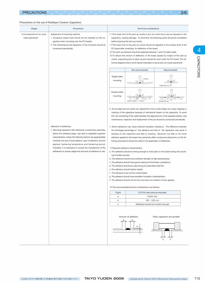
3.Considerations for auto-
matic placement
Adjustment of mounting machine
1. Excessive impact load should not be imposed on the ca-
pacitors when mounting onto the PC boards.
2. The maintenance and inspection of the mounters should be
conducted periodically.
Technical considerationsStages Precautions
1. If the lower limit of the pick-up nozzle is low, too much force may be imposed on the
capacitors, causing damage. To avoid this, the following points should be considered
before lowering the pick-up nozzle:
(1)The lower limit of the pick-up nozzle should be adjusted to the surface level of the
PC board after correcting for deflection of the board.
(2)The pick-up pressure should be adjusted between 1 and 3 N static loads.
(3)To reduce the amount of deflection of the board caused by impact of the pick-up
nozzle, supporting pins or back-up pins should be used under the PC board. The fol-
lowing diagrams show some typical examples of good pick-up nozzle placement:
Not recommended Recommended
Single-sided
mounting
Double-sided
mounting
2. As the alignment pin wears out, adjustment of the nozzle height can cause chipping or
cracking of the capacitors because of mechanical impact on the capacitors. To avoid
this, the monitoring of the width between the alignment pin in the stopped position, and
maintenance, inspection and replacement of the pin should be conducted periodically.
1. Some adhesives may cause reduced insulation resistance. The difference between
the shrinkage percentage of the adhesive and that of the capacitors may result in
stresses on the capacitors and lead to cracking. Moreover, too little or too much
adhesive applied to the board may adversely affect component placement, so the fol-
lowing precautions should be noted in the application of adhesives.
(1)Required adhesive characteristics
a. The adhesive should be strong enough to hold parts on the board during the mount-
ing & solder process.
b. The adhesive should have sufficient strength at high temperatures.
c. The adhesive should have good coating and thickness consistency.
d. The adhesive should be used during its prescribed shelf life.
e. The adhesive should harden rapidly
f. The adhesive must not be contaminated.
g. The adhesive should have excellent insulation characteristics.
h. The adhesive should not be toxic and have no emission of toxic gasses.
(2)The recommended amount of adhesives is as follows;
Figure 212/316 case sizes as examples
a 0.3mm min
b 100 ~120 μm
c Adhesives should not contact the pad
Selection of Adhesives
1. Mounting capacitors with adhesives in preliminary assembly,
before the soldering stage, may lead to degraded capacitor
characteristics unless the following factors are appropriately
checked; the size of land patterns, type of adhesive, amount
applied, hardening temperature and hardening period.
Therefore, it is imperative to consult the manufacturer of the
adhesives on proper usage and amounts of adhesive to use.
Precautions on the use of Multilayer Ceramic Capacitors

PRECAUTIONS
CA
PAC
ITOR
S
4
115△! 当社カタログをご使用の際には「当社製品に関するお断り」を必ずお読みください。 △! Please read the "Notice for TAIYO YUDEN products" before using this catalog.
4/6
4. Soldering Selection of Flux
1. Since flux may have a significant effect on the performance
of capacitors, it is necessary to verify the following condi-
tions prior to use;
(1)Flux used should be with less than or equal to 0.1 wt%
(equivelent to chroline) of halogenated content. Flux
having a strong acidity content should not be applied.
(2)When soldering capacitors on the board, the amount of
flux applied should be controlled at the optimum level.
(3)When using water-soluble flux, special care should be
taken to properly clean the boards.
Soldering
Temperature, time, amount of solder, etc. are specified in ac-
cordance with the following recommended conditions.
Sn-Zn solder paste can affect MLCC reliability performance.
Please contact us prior to usage.
1-1. When too much halogenated substance (Chlorine, etc.) content is used to activate
the flux, or highly acidic flux is used, an excessive amount of residue after soldering
may lead to corrosion of the terminal electrodes or degradation of insulation resis-
tance on the surface of the capacitors.
1-2. Flux is used to increase solderability in flow soldering, but if too much is applied, a
large amount of flux gas may be emitted and may detrimentally affect solderability. To
minimize the amount of flux applied, it is recommended to use a flux-bubbling system.
1-3. Since the residue of water-soluble flux is easily dissolved by water content in the
air, the residue on the surface of capacitors in high humidity conditions may cause a
degradation of insulation resistance and therefore affect the reliability of the compo-
nents. The cleaning methods and the capability of the machines used should also be
considered carefully when selecting water-soluble flux.
1-1. Preheating when soldering
Heating: Ceramic chip components should be preheated to within 100 to 130℃ of the
soldering.
Cooling: The temperature difference between the components and cleaning process
should not be greater than 100℃.
Ceramic chip capacitors are susceptible to thermal shock when exposed to rapid or concen-
trated heating or rapid cooling. Therefore, the soldering process must be conducted with
great care so as to prevent malfunction of the components due to excessive thermal shock.
Technical considerationsStages Precautions
Precautions on the use of Multilayer Ceramic Capacitors
Recommended conditions for soldering
[Reflow soldering]
Temperature profile
2. Because excessive dwell times can detrimentally affect solderability, soldering du-
ration should be kept as close to recommended times as possible.
[Wave soldering]
Temperature profile
Caution
1. The ideal condition is to have solder mass (fillet) controlled to 1/2 to 1/3 of the
thickness of the capacitor, as shown below:
Capacitor
PC board
Solder
Caution
1. Make sure the capacitors are preheated sufficiently.
2. The temperature difference between the capacitor and melted solder should not be
greater than 100 to 130℃
3. Cooling after soldering should be as gradual as possible.
4. Wave soldering must not be applied to the capacitors designated as for reflow sol-
dering only.
ピーク260℃以下10秒迄
ピーク260℃以下10秒迄
予熱150℃60秒以上
350℃以下3秒迄
120秒以上
60秒以上
予熱150℃
本加熱230℃以上40秒迄
※チップとはんだ温度との差が100~130℃以下になるよ うに十分予熱を行ってください。※回数は2回迄の保証となります。
※チップとはんだ温度との差が100~130℃以下になるよ うに十分予熱を行ってください。※回数は1回迄の保証となります。※リフロー仕様アイテムは除きます。
(※⊿T≦190℃(3216タイプ以下)、⊿T≦130℃(3225以上)。)※はんだコテは20Wで先端が1φ以下のものを推奨致します。※コテ先がチップに直接触れないようにご留意下さい。※回数は1回迄の保証となります。注:上記温度プロファイルは最大許容条件であり、 常にこれを推奨するものではございません。
温度(℃)300
200
100
0
温度(℃)300
200
100
0
温度(℃)400
300
200
100
0
徐冷
徐冷
徐冷
Peak 260℃ max10 sec max
Peak 260℃ max10 sec max
※Ceramic chip components should be preheated to within 100 to 130℃ of the soldering.※Assured to be reflow soldering for 2 times.
※Ceramic chip components should be preheated to within 100 to 130℃ of the soldering.※Assured to be wave soldering for 1 time.※Except for reflow soldering type.
(※⊿T≦190℃ (3216Type max), ⊿T≦130℃ (3225 Type min))※It is recommended to use 20W soldering iron and the tip is 1φ or less.※The soldering iron should not directly touch the components.※Assured to be soldering iron for 1 time.
Note: The above profiles are the maximum allowable soldering condition, therefore these profiles are not always recommended.
Temperature(℃)300
200
100
0
Temperature(℃)300
200
100
0
Temperature(℃)400
300
200
100
0
Preheating
150℃60 sec min
Graduallycooling
Graduallycooling
Graduallycooling
Heating above 230℃40 sec max
Preheating150℃
120 sec min
350℃ max3 sec max
60 sec min
⊿T⊿T
(Pb free soldering)
(Pb free soldering)
(Pb free soldering)
ピーク260℃以下10秒迄
ピーク260℃以下10秒迄
予熱150℃60秒以上
350℃以下3秒迄
120秒以上
60秒以上
予熱150℃
本加熱230℃以上40秒迄
※チップとはんだ温度との差が100~130℃以下になるよ うに十分予熱を行ってください。※回数は2回迄の保証となります。
※チップとはんだ温度との差が100~130℃以下になるよ うに十分予熱を行ってください。※回数は1回迄の保証となります。※リフロー仕様アイテムは除きます。
(※⊿T≦190℃(3216タイプ以下)、⊿T≦130℃(3225以上)。)※はんだコテは20Wで先端が1φ以下のものを推奨致します。※コテ先がチップに直接触れないようにご留意下さい。※回数は1回迄の保証となります。注:上記温度プロファイルは最大許容条件であり、 常にこれを推奨するものではございません。
温度(℃)300
200
100
0
温度(℃)300
200
100
0
温度(℃)400
300
200
100
0
徐冷
徐冷
徐冷
Peak 260℃ max10 sec max
Peak 260℃ max10 sec max
※Ceramic chip components should be preheated to within 100 to 130℃ of the soldering.※Assured to be reflow soldering for 2 times.
※Ceramic chip components should be preheated to within 100 to 130℃ of the soldering.※Assured to be wave soldering for 1 time.※Except for reflow soldering type.
(※⊿T≦190℃ (3216Type max), ⊿T≦130℃ (3225 Type min))※It is recommended to use 20W soldering iron and the tip is 1φ or less.※The soldering iron should not directly touch the components.※Assured to be soldering iron for 1 time.
Note: The above profiles are the maximum allowable soldering condition, therefore these profiles are not always recommended.
Temperature(℃)300
200
100
0
Temperature(℃)300
200
100
0
Temperature(℃)400
300
200
100
0
Preheating
150℃60 sec min
Graduallycooling
Graduallycooling
Graduallycooling
Heating above 230℃40 sec max
Preheating150℃
120 sec min
350℃ max3 sec max
60 sec min
⊿T⊿T
(Pb free soldering)
(Pb free soldering)
(Pb free soldering)

PRECAUTIONS
CA
PAC
ITOR
S
4
117△! 当社カタログをご使用の際には「当社製品に関するお断り」を必ずお読みください。 △! Please read the "Notice for TAIYO YUDEN products" before using this catalog.
5/6
[Hand soldering]
Temperature profile
5.Cleaning Cleaning conditions
1. When cleaning the PC board after the capacitors are all
mounted, select the appropriate cleaning solution according
to the type of flux used and purpose of the cleaning (e.g.
to remove soldering flux or other materials from the produc-
tion process.)
2. Cleaning conditions should be determined after verifying,
through a test run, that the cleaning process does not affect
the capacitor's characteristics.
1. The use of inappropriate solutions can cause foreign substances such as flux residue
to adhere to the capacitor or deteriorate the capacitor's outer coating, resulting in a
degradation of the capacitor's electrical properties (especially insulation resistance).
2. Inappropriate cleaning conditions (insufficient or excessive cleaning) may detrimen-
tally affect the performance of the capacitors.
(1)Excessive cleaning
In the case of ultrasonic cleaning, too much power output can cause excessive vibra-
tion of the PC board which may lead to the cracking of the capacitor or the soldered
portion, or decrease the terminal electrodes' strength. Thus the following conditions
should be carefully checked;
Ultrasonic output Below 20 W/ℓ
Ultrasonic frequency Below 40 kHz
Ultrasonic washing period 5 min. or less
4. Soldering
6.Post cleaning processes 1. With some type of resins a decomposition gas or chemical
reaction vapor may remain inside the resin during the hard-
ening period or while left under normal storage conditions
resulting in the deterioration of the capacitor's performance.
2. When a resin's hardening temperature is higher than the
capacitor's operating temperature, the stresses generated by
the excess heat may lead to capacitor damage or destruction.
The use of such resins, molding materials etc. is not recom-
mended.
Breakaway PC boards (splitting along perforations)
1. When splitting the PC board after mounting capacitors and
other components, care is required so as not to give any
stresses of deflection or twisting to the board.
2. Board separation should not be done manually, but by us-
ing the appropriate devices.
Mechanical considerations
1. Be careful not to subject the capacitors to excessive me-
chanical shocks.
(1)If ceramic capacitors are dropped onto the floor or a
hard surface, they should not be used.
(2)When handling the mounted boards, be careful that the
mounted components do not come in contact with or
bump against other boards or components.
7.Handling
Technical considerationsStages Precautions
Precautions on the use of Multilayer Ceramic Capacitors
Caution
1. Use a 20W soldering iron with a maximum tip diameter of 1.0 mm.
2. The soldering iron should not directly touch the capacitor.
ピーク260℃以下10秒迄
ピーク260℃以下10秒迄
予熱150℃60秒以上
350℃以下3秒迄
120秒以上
60秒以上
予熱150℃
本加熱230℃以上40秒迄
※チップとはんだ温度との差が100~130℃以下になるよ うに十分予熱を行ってください。※回数は2回迄の保証となります。
※チップとはんだ温度との差が100~130℃以下になるよ うに十分予熱を行ってください。※回数は1回迄の保証となります。※リフロー仕様アイテムは除きます。
(※⊿T≦190℃(3216タイプ以下)、⊿T≦130℃(3225以上)。)※はんだコテは20Wで先端が1φ以下のものを推奨致します。※コテ先がチップに直接触れないようにご留意下さい。※回数は1回迄の保証となります。注:上記温度プロファイルは最大許容条件であり、 常にこれを推奨するものではございません。
温度(℃)300
200
100
0
温度(℃)300
200
100
0
温度(℃)400
300
200
100
0
徐冷
徐冷
徐冷
Peak 260℃ max10 sec max
Peak 260℃ max10 sec max
※Ceramic chip components should be preheated to within 100 to 130℃ of the soldering.※Assured to be reflow soldering for 2 times.
※Ceramic chip components should be preheated to within 100 to 130℃ of the soldering.※Assured to be wave soldering for 1 time.※Except for reflow soldering type.
(※⊿T≦190℃ (3216Type max), ⊿T≦130℃ (3225 Type min))※It is recommended to use 20W soldering iron and the tip is 1φ or less.※The soldering iron should not directly touch the components.※Assured to be soldering iron for 1 time.
Note: The above profiles are the maximum allowable soldering condition, therefore these profiles are not always recommended.
Temperature(℃)300
200
100
0
Temperature(℃)300
200
100
0
Temperature(℃)400
300
200
100
0
Preheating
150℃60 sec min
Graduallycooling
Graduallycooling
Graduallycooling
Heating above 230℃40 sec max
Preheating150℃
120 sec min
350℃ max3 sec max
60 sec min
⊿T⊿T
(Pb free soldering)
(Pb free soldering)
(Pb free soldering)

PRECAUTIONS
CA
PAC
ITOR
S
4
119△! 当社カタログをご使用の際には「当社製品に関するお断り」を必ずお読みください。 △! Please read the "Notice for TAIYO YUDEN products" before using this catalog.
6/6
8.Storage conditions Storage
1. To maintain the solderability of terminal electrodes and to
keep the packaging material in good condition, care must
be taken to control temperature and humidity in the storage
area. Humidity should especially be kept as low as possible.
・Recommended conditions
Ambient temperature Below 30℃
Humidity Below 70% RH
The ambient temperature must be kept below 40℃. Even
under ideal storage conditions capacitor electrode solder-
ability decreases as time passes, so should be used within
6 months from the time of delivery.
・Ceramic chip capacitors should be kept where no chlorine or
sulfur exists in the air.
2. The capacitance value of high dielectric constant capacitors
(type 2 &3) will gradually decrease with the passage of time,
so this should be taken into consideration in the circuit design.
If such a capacitance reduction occurs, a heat treatment of
150℃ for 1hour will return the capacitance to its initial level.
1. If the parts are stored in a high temperature and humidity environment, problems
such as reduced solderability caused by oxidation of terminal electrodes and dete-
rioration of taping/packaging materials may take place. For this reason, components
should be used within 6 months from the time of delivery. If exceeding the above
period, please check solderability before using the capacitors.
Technical considerationsStages Precautions
Precautions on the use of Multilayer Ceramic Capacitors


![Notice for TAIYO YUDEN Products · Notice for TAIYO YUDEN Products [ For High Quality and/or Reliability Equipment (Automotive / Industrial Equipment) ] Please read this notice before](https://img.pdfslide.us/doc/110x75/5b6d7e657f8b9a0d578cf4d3/notice-for-taiyo-yuden-products-notice-for-taiyo-yuden-products-for-high-quality.jpg)
![Notice for TAIYO YUDEN Products - Mouser · PDF fileNotice for TAIYO YUDEN Products [ For High Quality and/or Reliability Equipment (Automotive / Industrial Equipment) ] Please read](https://img.pdfslide.us/doc/110x75/5a7a28887f8b9adf778d544d/notice-for-taiyo-yuden-products-mouser-for-taiyo-yuden-products-for-high-quality.jpg)


![Notice for TAIYO YUDEN Products (General Environment) ] · PDF fileNotice for TAIYO YUDEN Products [ For General Electronic Equipment (General Environment) ] Please read this notice](https://img.pdfslide.us/doc/110x75/5a7a28887f8b9adf778d5450/notice-for-taiyo-yuden-products-general-environment-for-taiyo-yuden-products.jpg)


![Notice for TAIYO YUDEN Products [ For General … for TAIYO YUDEN Products [ For General Electronic Equipment ] Please read this notice before using the TAIYO YUDEN products. REMINDERS](https://img.pdfslide.us/doc/110x75/5c85e46209d3f2700a8b9840/notice-for-taiyo-yuden-products-for-general-for-taiyo-yuden-products-for-general.jpg)

![Notice for TAIYO YUDEN Products (General … · Notice for TAIYO YUDEN Products [ For General Electronic Equipment (General Environment) ] Please read this notice before using the](https://img.pdfslide.us/doc/110x75/5b9dc92509d3f2a4348c8986/notice-for-taiyo-yuden-products-general-notice-for-taiyo-yuden-products-for.jpg)


![Notice for TAIYO YUDEN Products (General Environment) ]](https://img.pdfslide.us/doc/110x75/61d01fc6eb7c74517f018363/notice-for-taiyo-yuden-products-general-environment-.jpg)
![Notice for TAIYO YUDEN Products (General … for TAIYO YUDEN Products [ For General Electronic Equipment (General Environment) ] Please read this notice before using the TAIYO YUDEN](https://img.pdfslide.us/doc/110x75/5aa4c9217f8b9ac8748c5d02/notice-for-taiyo-yuden-products-general-for-taiyo-yuden-products-for-general.jpg)