Embed Size (px)
Citation preview
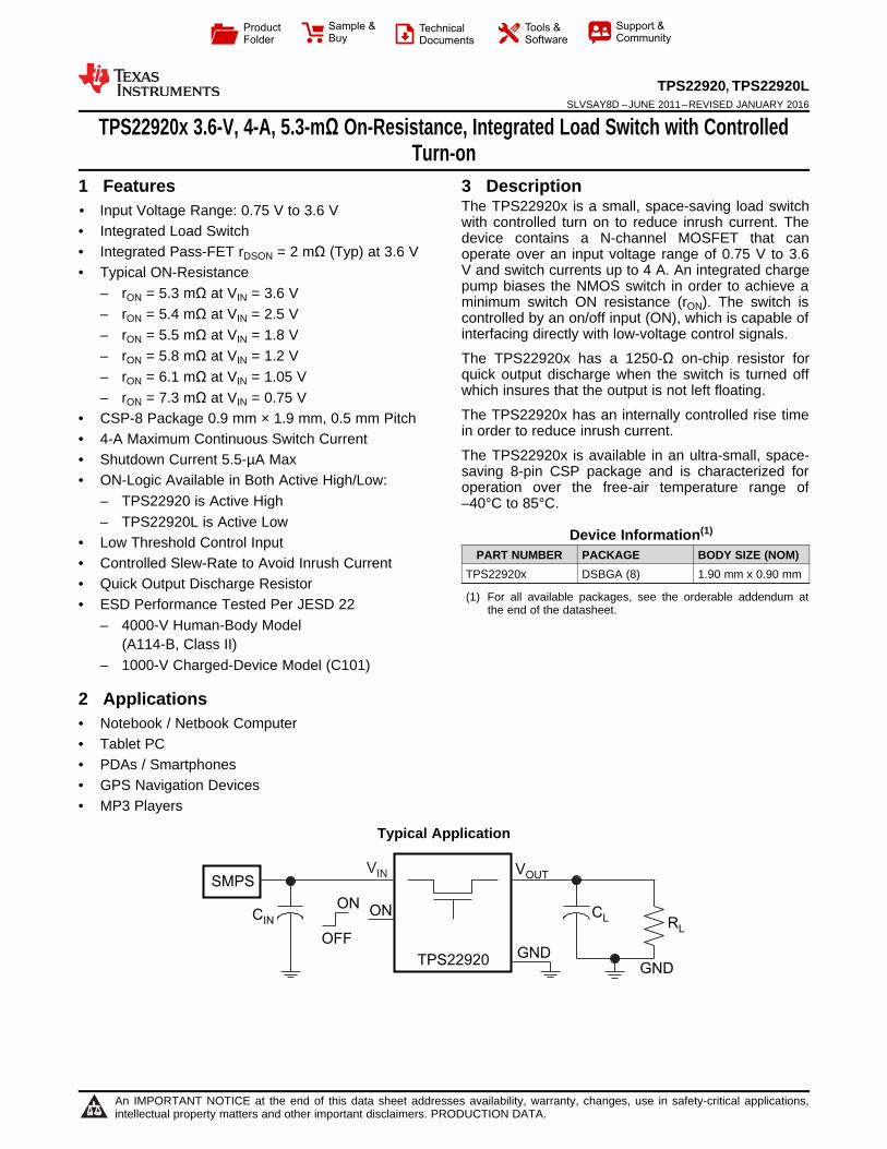
SMPS
OFF
ON
TPS22920
VOUT
RL
CL
GND
ON
GND
CIN
VIN
Product
Folder
Sample &Buy
Technical
Documents
Tools &
Software
Support &Community
An IMPORTANT NOTICE at the end of this data sheet addresses availability, warranty, changes, use in safety-critical applications,intellectual property matters and other important disclaimers. PRODUCTION DATA.
TPS22920, TPS22920LSLVSAY8D –JUNE 2011–REVISED JANUARY 2016
TPS22920x 3.6-V, 4-A, 5.3-mΩ On-Resistance, Integrated Load Switch with ControlledTurn-on
1
1 Features1• Input Voltage Range: 0.75 V to 3.6 V• Integrated Load Switch• Integrated Pass-FET rDSON = 2 mΩ (Typ) at 3.6 V• Typical ON-Resistance
– rON = 5.3 mΩ at VIN = 3.6 V– rON = 5.4 mΩ at VIN = 2.5 V– rON = 5.5 mΩ at VIN = 1.8 V– rON = 5.8 mΩ at VIN = 1.2 V– rON = 6.1 mΩ at VIN = 1.05 V– rON = 7.3 mΩ at VIN = 0.75 V
• CSP-8 Package 0.9 mm × 1.9 mm, 0.5 mm Pitch• 4-A Maximum Continuous Switch Current• Shutdown Current 5.5-µA Max• ON-Logic Available in Both Active High/Low:
– TPS22920 is Active High– TPS22920L is Active Low
• Low Threshold Control Input• Controlled Slew-Rate to Avoid Inrush Current• Quick Output Discharge Resistor• ESD Performance Tested Per JESD 22
– 4000-V Human-Body Model(A114-B, Class II)
– 1000-V Charged-Device Model (C101)
2 Applications• Notebook / Netbook Computer• Tablet PC• PDAs / Smartphones• GPS Navigation Devices• MP3 Players
3 DescriptionThe TPS22920x is a small, space-saving load switchwith controlled turn on to reduce inrush current. Thedevice contains a N-channel MOSFET that canoperate over an input voltage range of 0.75 V to 3.6V and switch currents up to 4 A. An integrated chargepump biases the NMOS switch in order to achieve aminimum switch ON resistance (rON). The switch iscontrolled by an on/off input (ON), which is capable ofinterfacing directly with low-voltage control signals.
The TPS22920x has a 1250-Ω on-chip resistor forquick output discharge when the switch is turned offwhich insures that the output is not left floating.
The TPS22920x has an internally controlled rise timein order to reduce inrush current.
The TPS22920x is available in an ultra-small, space-saving 8-pin CSP package and is characterized foroperation over the free-air temperature range of–40°C to 85°C.
Device Information(1)
PART NUMBER PACKAGE BODY SIZE (NOM)TPS22920x DSBGA (8) 1.90 mm x 0.90 mm
(1) For all available packages, see the orderable addendum atthe end of the datasheet.
Typical Application
2
TPS22920, TPS22920LSLVSAY8D –JUNE 2011–REVISED JANUARY 2016 www.ti.com
Product Folder Links: TPS22920 TPS22920L
Submit Documentation Feedback Copyright © 2011–2016, Texas Instruments Incorporated
Table of Contents1 Features .................................................................. 12 Applications ........................................................... 13 Description ............................................................. 14 Revision History..................................................... 25 Device Comparison Table ..................................... 36 Pin Configuration and Functions ......................... 37 Specifications......................................................... 4
7.1 Absolute Maximum Ratings ..................................... 47.2 ESD Ratings.............................................................. 47.3 Recommended Operating Conditions....................... 47.4 Thermal Information .................................................. 47.5 Electrical Characteristics........................................... 57.6 Switching Characteristics: VIN = 3.6 V ...................... 57.7 Switching Characteristics: VIN = 0.9 V ...................... 57.8 Typical DC Characteristics........................................ 67.9 TPS22920 Typical AC Characteristics...................... 77.10 TPS22920L Typical AC Characteristics................ 10
8 Parametric Measurement Information ............... 13
9 Detailed Description ............................................ 159.1 Overview ................................................................. 159.2 Functional Block Diagram ....................................... 159.3 Feature Description................................................. 159.4 Device Functional Modes........................................ 15
10 Application and Implementation........................ 1610.1 Application Information.......................................... 1610.2 Typical Application ............................................... 16
11 Power Supply Recommendations ..................... 1912 Layout................................................................... 19
12.1 Layout Guidelines ................................................. 1912.2 Layout Example .................................................... 19
13 Device and Documentation Support ................. 2013.1 Related Links ........................................................ 2013.2 Trademarks ........................................................... 2013.3 Electrostatic Discharge Caution............................ 2013.4 Glossary ................................................................ 20
14 Mechanical, Packaging, and OrderableInformation ........................................................... 20
4 Revision History
Changes from Revision C (April 2015) to Revision D Page
• Added Information about backside coating to Device Comparison table .............................................................................. 3
Changes from Revision November 2014 (B) to Revision C Page
• Added TPS22920L to the datasheet. ..................................................................................................................................... 1
Changes from Revision A (July 2013) to Revision B Page
• Added Pin Configuration and Functions section, Handling Rating table, Feature Description section, DeviceFunctional Modes, Application and Implementation section, Power Supply Recommendations section, Layoutsection, Device and Documentation Support section, and Mechanical, Packaging, and Orderable Informationsection ................................................................................................................................................................................... 1
Changes from Original (June 2011) to Revision A Page
• Updated swapped image issue. ............................................................................................................................................. 7
D
C
B
A
YZP PACKAGE
D
C
B
A
2 1 1 2
LASER MARKING
VIEW
BUMP VIEW
3
TPS22920, TPS22920Lwww.ti.com SLVSAY8D –JUNE 2011–REVISED JANUARY 2016
Product Folder Links: TPS22920 TPS22920L
Submit Documentation FeedbackCopyright © 2011–2016, Texas Instruments Incorporated
5 Device Comparison Table
(1) This feature discharges the output of the switch to ground through a 1250-Ω resistor, preventing the output from floating. See OutputPull-Down.
(2) CSP (DSBGA) devices manufactured with backside coating have an increased resistance to cracking due to the increased physicalstrength of the package. Devices with backside coating are highly encouraged for new designs.
ORDERABLE PARTNUMBER
RON (TYP)AT 3.6 V
RISE TIME(TYP) at 3.6V
QUICK OUTPUTDISCHARGE (1)
BACKSIDECOATING (2) ENABLE
TPS22920YZPR 5.3 mΩ 880 µS Yes No Active HighTPS22920YZPRB 5.3 mΩ 880 µS Yes Yes Active HighTPS22920LYZPR 5.3 mΩ 627 µS Yes Yes Active Low
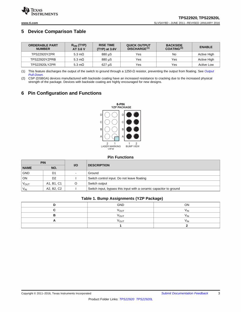
6 Pin Configuration and Functions
8-PIN
Pin FunctionsPIN
I/O DESCRIPTIONNAME NO.GND D1 - GroundON D2 I Switch control input. Do not leave floatingVOUT A1, B1, C1 O Switch outputVIN A2, B2, C2 I Switch input, bypass this input with a ceramic capacitor to ground
Table 1. Bump Assignments (YZP Package)D GND ONC VOUT VIN
B VOUT VIN
A VOUT VIN
1 2
4
TPS22920, TPS22920LSLVSAY8D –JUNE 2011–REVISED JANUARY 2016 www.ti.com
Product Folder Links: TPS22920 TPS22920L
Submit Documentation Feedback Copyright © 2011–2016, Texas Instruments Incorporated
(1) Stresses beyond those listed under Absolute Maximum Ratings may cause permanent damage to the device. These are stress only,and functional operation of the device at these or any other conditions beyond those indicated under Recommended OperatingConditions is not implied. Exposure to absolute-maximum-rated conditions for extended periods may affect device reliability.
7 Specifications
7.1 Absolute Maximum Ratings (1)
MIN MAX UNITVIN Input voltage range –0.3 4 VVOUT Output voltage range VIN + 0.3 VVON Input voltage range –0.3 4 VIMAX Maximum Continuous Switch Current 4 AIPLS Maximum Pulsed Switch Current, pulse <300 µS, 2% duty cycle 6 ATJ Maximum junction temperature 125 °CTstg Storage temperature range –65 150 °C
(1) JEDEC document JEP155 states that 500-V HBM allows safe manufacturing with a standard ESD control process. Manufacturing withless than 500-V HBM is possible with the necessary precautions.
(2) JEDEC document JEP157 states that 250-V CDM allows safe manufacturing with a standard ESD control process. Manufacturing withless than 250-V CDM is possible with the necessary precautions.
7.2 ESD RatingsVALUE UNIT
V(ESD) Electrostatic dischargeHuman-body model (HBM), per ANSI/ESDA/JEDEC JS-001 (1) ±4000
VCharged-device model (CDM), per JEDEC specification JESD22-C101 (2) ±1000
(1) See Input Capacitor section in Application Information.
7.3 Recommended Operating ConditionsMIN MAX UNIT
VIN Input voltage range 0.75 3.6 VVOUT Output voltage range VIN V
VIH High-level input voltage, ONVIN = 2.5 V to 3.6 V 1.2 3.6 VVIN = 0.75 V to 2.49 V 0.9 3.6 V
VIL Low-level input voltage, ONVIN = 2.5 V to 3.6 V 0.6 VVIN = 0.75 V to 2.49 V 0.4 V
TA Operating free-air temperature range –40 85 °CCIN Input Capacitor 1 (1) µF
(1) For more information about traditional and new thermal metrics, see the IC Package Thermal Metrics application report, SPRA953.
7.4 Thermal Information
THERMAL METRIC (1)TPS22920x
UNITYZP8 PINS
RθJA Junction-to-ambient thermal resistance 130
°C/WRθJC(top) Junction-to-case (top) thermal resistance 54RθJB Junction-to-board thermal resistance 51ψJT Junction-to-top characterization parameter 1ψJB Junction-to-board characterization parameter 50
5
TPS22920, TPS22920Lwww.ti.com SLVSAY8D –JUNE 2011–REVISED JANUARY 2016
Product Folder Links: TPS22920 TPS22920L
Submit Documentation FeedbackCopyright © 2011–2016, Texas Instruments Incorporated
(1) Typical values are at VIN = 3.3 V and TA = 25°C.(2) See Output Pull-Down .
7.5 Electrical CharacteristicsUnless otherwise noted, VIN = 0.75 V to 3.6 V
PARAMETER TEST CONDITIONS TA MIN TYP (1) MAX UNIT
IIN Quiescent Current IOUT = 0, Switchenabled
VIN = 3.6 V
Full
68 160µA
VIN = 2.5 V 40 70VIN = 1.8 V 25 350
µAVIN = 1.2 V 103 200VIN = 1.05 V 78 110
µAVIN = 0.75 V 37 70
IIN(leak)Off Supply Current (AfterPull Down) Switch disabled, VOUT = 0 Full 5.5 µA
rON On-Resistance
VIN = 3.6 V, IOUT = –200 mA25°C 5.3 8.8
mΩFull 9.8
VIN = 2.5 V, IOUT = –200 mA25°C 5.4 8.9
mΩFull 9.9
VIN = 1.8 V, IOUT = –200 mA25°C 5.5 9.1
mΩFull 10.1
VIN = 1.2 V, IOUT = –200 mA25°C 5.8 9.4
mΩFull 10.4
VIN = 1.05 V, IOUT = –200 mA25°C 6.1 9.7
mΩFull 10.8
VIN = 0.75 V, IOUT = –200 mA25°C 7.3 11.0
mΩFull 12.4
RPD Output pull downresistance (2) VIN = 3.3 V, Switch disabled, IOUT = 3 mA Full 1250 1500 Ω
ION ON input leakage current VON = 0.9 V to 3.6 V or GND Full 0.1 µA
7.6 Switching Characteristics: VIN = 3.6 VTA = 25°C (unless otherwise noted)
PARAMETER TEST CONDITIONTPS22920 TPS22920L
UNITTYP TYP
tON Turn-ON time RL = 10 Ω, CL = 0.1 µF, VIN = 3.6 V 970 663
µstOFF Turn-OFF time RL = 10 Ω, CL = 0.1 µF, VIN = 3.6 V 3 2tr VOUT Rise time RL = 10 Ω, CL = 0.1 µF, VIN = 3.6 V 880 627tf VOUT Fall time RL = 10 Ω, CL = 0.1 µF, VIN = 3.6 V 2 2
7.7 Switching Characteristics: VIN = 0.9 VTA = 25°C (unless otherwise noted)
PARAMETER TEST CONDITIONTPS22920 TPS22920L
UNITTYP TYP
tON Turn-ON time RL = 10 Ω, CL = 0.1 µF, VIN = 0.9 V 840 840
µstOFF Turn-OFF time RL = 10 Ω, CL = 0.1 µF, VIN = 0.9 V 16 16tr VOUT Rise time RL = 10 Ω, CL = 0.1 µF, VIN = 0.9 V 470 470tf VOUT Fall time RL = 10 Ω, CL = 0.1 µF, VIN = 0.9 V 5 5
0
0.5
1
1.5
2
2.5
3
3.5
4
0 0.2 0.4 0.6 0.8 1 1.2
VON (V)
VO
UT
(V)
VIN = 0.75
VIN = 1.05
VIN = 1.2
VIN = 1.8V
VIN = 2.5
VIN = 3.6
G000
0
20
40
60
80
100
120
140
160
180
200
220
0 1 2 3 4
Voltage (V)
IIN
_Q
(µ
A)
−40C
25C
85C
G000
0
400
800
1200
1600
2000
2400
2800
3200
3600
0 0.5 1 1.5 2 2.5 3 3.5 4
Voltage (V)
IIN
_Leak (
nA
)
−40C
25C
85C
G000
0
1
2
3
4
5
6
7
8
9
10
11
0 0.5 1 1.5 2 2.5 3 3.5 4
Voltage (V)
Ron (
mW
)
−40C
25C
85C
G000
0
1
2
3
4
5
6
7
8
9
10
11
−40 −15 10 35 60 85
Temperature (°C)
Ron (
mW
)
VIN = 0.75
VIN = 1.05
VIN = 1.2
VIN = 1.8V
VIN = 2.5
VIN = 3.6
G000
6
TPS22920, TPS22920LSLVSAY8D –JUNE 2011–REVISED JANUARY 2016 www.ti.com
Product Folder Links: TPS22920 TPS22920L
Submit Documentation Feedback Copyright © 2011–2016, Texas Instruments Incorporated
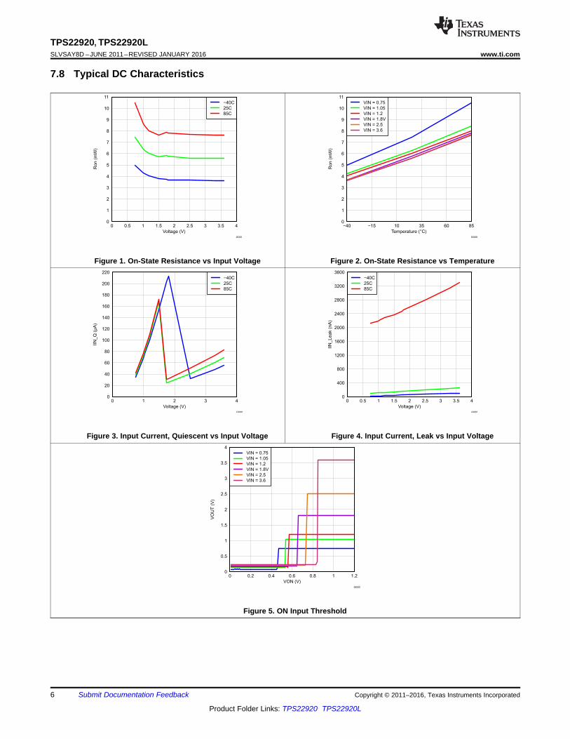
7.8 Typical DC Characteristics
Figure 1. On-State Resistance vs Input Voltage Figure 2. On-State Resistance vs Temperature
Figure 3. Input Current, Quiescent vs Input Voltage Figure 4. Input Current, Leak vs Input Voltage
Figure 5. ON Input Threshold
0
100
200
300
400
500
600
700
800
900
1000
1100
1200
−40 −15 10 35 60 85
Temperature (°C)
tOn
(µ
s)
VIN = 0.9V, CL = 0.1 µF, RL = 10 Ohms
G000
0
5
10
15
20
25
30
35
40
45
50
55
60
−40 −15 10 35 60 85
Temperature (°C)
tOff (
µs)
VIN = 0.9V, CL = 0.1 µF, RL = 10 Ohms
G000
0
100
200
300
400
500
600
700
800
900
1000
1100
−40 −15 10 35 60 85
Temperature (°C)
tRis
e (
µs)
VIN = 3.6V, CL = 0.1 µF, RL = 10 Ohms
G000
0
0.2
0.4
0.6
0.8
1
1.2
1.4
1.6
1.8
2
−40 −15 10 35 60 85
Temperature (°C)
tFall
(µs)
VIN = 3.6V, CL = 0.1 µF, RL = 10 Ohms
G000
0
100
200
300
400
500
600
700
800
900
1000
1100
1200
1300
−40 −15 10 35 60 85
Temperature (°C)
tOn
(µ
s)
VIN = 3.6V, CL = 0.1 µF, RL = 10 Ohms
G000
0
0.5
1
1.5
2
2.5
3
3.5
4
−40 −15 10 35 60 85
Temperature (°C)
tOff (
µs)
VIN = 3.6V, CL = 0.1 µF, RL = 10 Ohms
G000
7
TPS22920, TPS22920Lwww.ti.com SLVSAY8D –JUNE 2011–REVISED JANUARY 2016
Product Folder Links: TPS22920 TPS22920L
Submit Documentation FeedbackCopyright © 2011–2016, Texas Instruments Incorporated
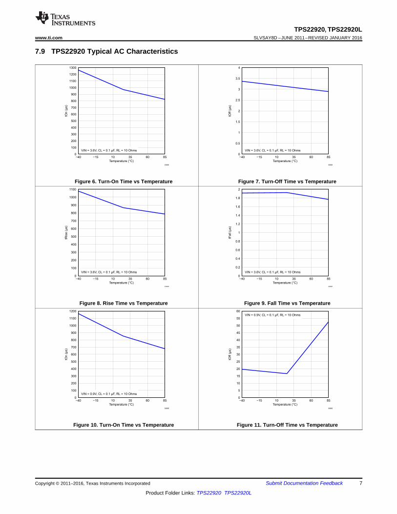
7.9 TPS22920 Typical AC Characteristics
Figure 6. Turn-On Time vs Temperature Figure 7. Turn-Off Time vs Temperature
Figure 8. Rise Time vs Temperature Figure 9. Fall Time vs Temperature
Figure 10. Turn-On Time vs Temperature Figure 11. Turn-Off Time vs Temperature
0
200
400
600
800
1000
1200
1400
1600
0 0.5 1 1.5 2 2.5 3 3.5 4VIN (V)
tRis
e (µ
s)
−40C25C85C
CL = 20 µF, RL = 10 Ohms, VON = 1.8V
G000
0
200
400
600
800
1000
1200
1400
1600
1800
0 0.5 1 1.5 2 2.5 3 3.5 4VIN (V)
tRis
e (µ
s)
−40C25C85C
CL = 0.1 µF, RL = 10 Ohms, VON = 1.8V
G000
0
100
200
300
400
500
600
700
800
−40 −15 10 35 60 85
Temperature (°C)
tRis
e (
µs)
VIN = 0.9V, CL = 0.1 µF, RL = 10 Ohms
G000
0
0.5
1
1.5
2
2.5
3
3.5
4
4.5
5
5.5
6
6.5
7
−40 −15 10 35 60 85
Temperature (°C)
tFall
(µs)
VIN = 0.9V, CL = 0.1 µF, RL = 10 Ohms
G000
8
TPS22920, TPS22920LSLVSAY8D –JUNE 2011–REVISED JANUARY 2016 www.ti.com
Product Folder Links: TPS22920 TPS22920L
Submit Documentation Feedback Copyright © 2011–2016, Texas Instruments Incorporated
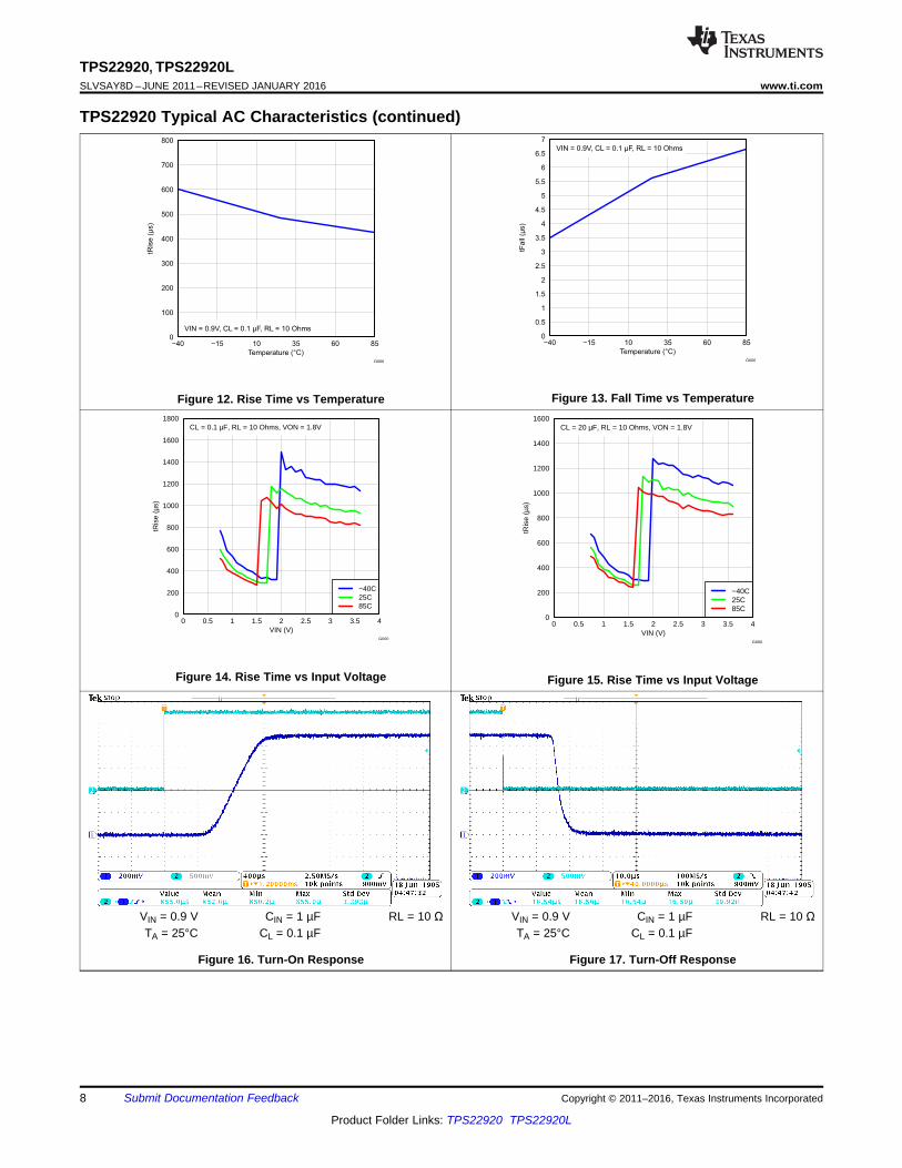
TPS22920 Typical AC Characteristics (continued)
Figure 12. Rise Time vs Temperature Figure 13. Fall Time vs Temperature
Figure 14. Rise Time vs Input Voltage Figure 15. Rise Time vs Input Voltage
VIN = 0.9 V CIN = 1 µF RL = 10 ΩTA = 25°C CL = 0.1 µF
Figure 16. Turn-On Response
VIN = 0.9 V CIN = 1 µF RL = 10 ΩTA = 25°C CL = 0.1 µF
Figure 17. Turn-Off Response
9
TPS22920, TPS22920Lwww.ti.com SLVSAY8D –JUNE 2011–REVISED JANUARY 2016
Product Folder Links: TPS22920 TPS22920L
Submit Documentation FeedbackCopyright © 2011–2016, Texas Instruments Incorporated
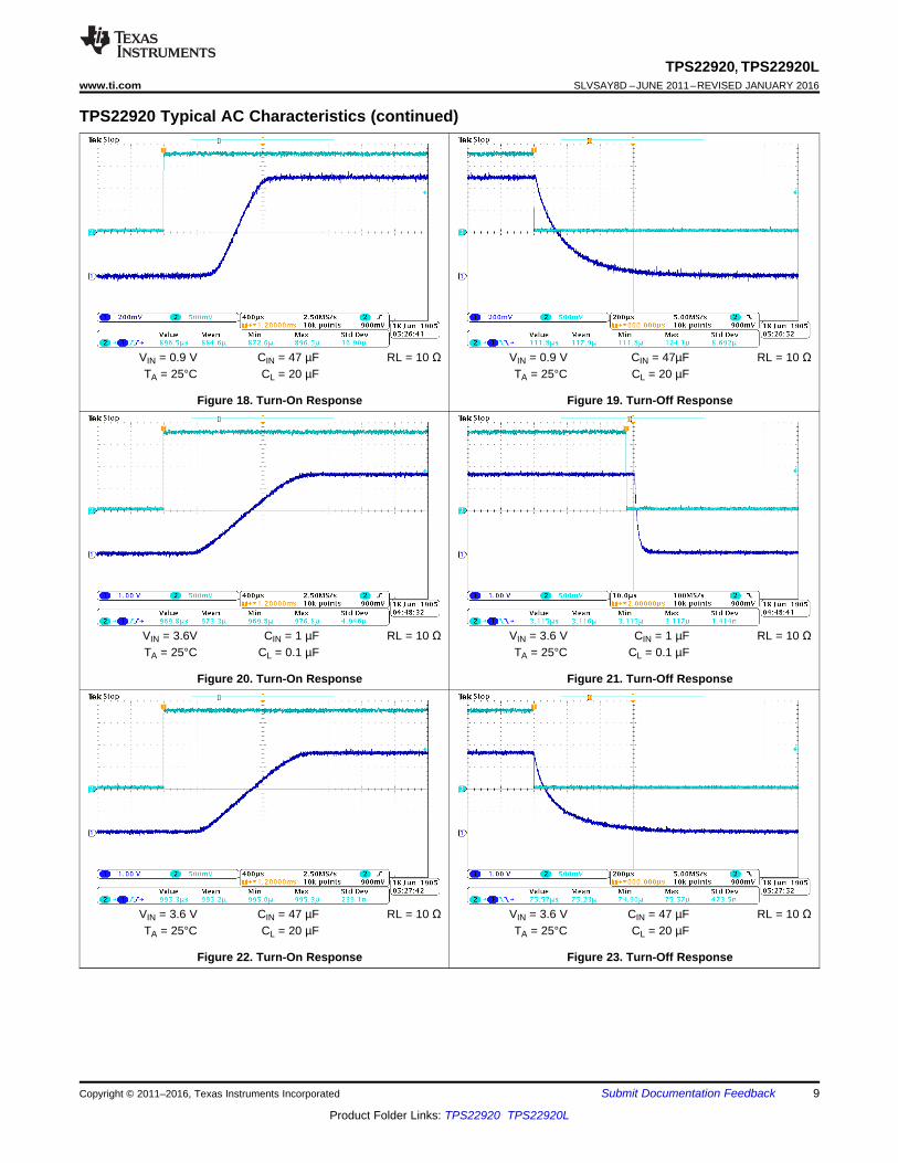
TPS22920 Typical AC Characteristics (continued)
VIN = 0.9 V CIN = 47 µF RL = 10 ΩTA = 25°C CL = 20 µF
Figure 18. Turn-On Response
VIN = 0.9 V CIN = 47µF RL = 10 ΩTA = 25°C CL = 20 µF
Figure 19. Turn-Off Response
VIN = 3.6V CIN = 1 µF RL = 10 ΩTA = 25°C CL = 0.1 µF
Figure 20. Turn-On Response
VIN = 3.6 V CIN = 1 µF RL = 10 ΩTA = 25°C CL = 0.1 µF
Figure 21. Turn-Off Response
VIN = 3.6 V CIN = 47 µF RL = 10 ΩTA = 25°C CL = 20 µF
Figure 22. Turn-On Response
VIN = 3.6 V CIN = 47 µF RL = 10 ΩTA = 25°C CL = 20 µF
Figure 23. Turn-Off Response
0
200
400
600
800
1000
1200
0 0.5 1 1.5 2 2.5 3 3.5 4
t R (
µs)
VIN (V)
-40C
25C
85C
C015
0
1
2
3
4
5
6
7
0 0.5 1 1.5 2 2.5 3 3.5 4
t F (
µs)
VIN (V)
-40C
25C
85C
C016
0
1
2
3
4
5
6
-40 -15 10 35 60 85
t F (
µs)
Temperature ( C)
VIN = 0.9V
VIN = 3.6V
C001
CL= 0.1µF, RL = 10 , VON = 3.6V 0
100
200
300
400
500
600
700
800
900
-40 -15 10 35 60 85
t R (
µs)
Temperature ( C)
VIN = 0.9V
VIN = 3.6V
C004
CL= 0.1µF, RL = 10 , VON = 3.6V
0
200
400
600
800
1000
1200
1400
-40 -15 10 35 60 85
t ON (
µs)
Temperature ( C)
VIN = 0.9V
VIN = 3.6V
C003
CL= 0.1µF, RL = 10 , VON = 3.6V 0
2
4
6
8
10
12
14
16
18
-40 -15 10 35 60 85
t OF
F (
µs)
Temperature ( C)
VIN = 0.9V
VIN = 3.6V
C002
CL= 0.1µF, RL = 10 , VON = 3.6V
10
TPS22920, TPS22920LSLVSAY8D –JUNE 2011–REVISED JANUARY 2016 www.ti.com
Product Folder Links: TPS22920 TPS22920L
Submit Documentation Feedback Copyright © 2011–2016, Texas Instruments Incorporated
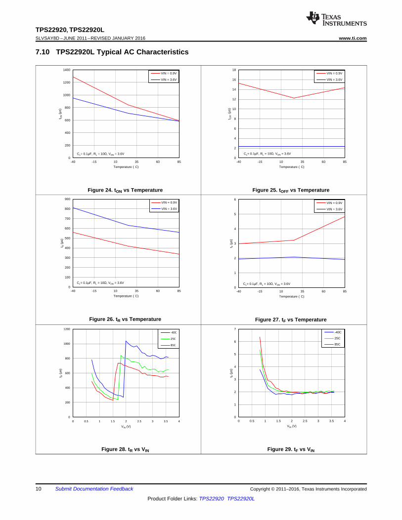
7.10 TPS22920L Typical AC Characteristics
Figure 24. tON vs Temperature Figure 25. tOFF vs Temperature
Figure 26. tR vs Temperature Figure 27. tF vs Temperature
Figure 28. tR vs VIN Figure 29. tF vs VIN
0
500
1000
1500
2000
2500
0 1 2 3 4
t ON (
µs)
VIN (V)
-40C
25C
85C
C018
0
200
400
600
800
1000
1200
1400
0 0.5 1 1.5 2 2.5 3 3.5 4
t D (
µs)
VIN (V)
-40C
25C
85C
C017
0
5
10
15
20
25
30
0 0.5 1 1.5 2 2.5 3 3.5 4
t OF
F (
µs)
VIN (V)
-40C
25C
85C
C018
CL= 0.1µF, RL = 10 , VON = 3.6V
11
TPS22920, TPS22920Lwww.ti.com SLVSAY8D –JUNE 2011–REVISED JANUARY 2016
Product Folder Links: TPS22920 TPS22920L
Submit Documentation FeedbackCopyright © 2011–2016, Texas Instruments Incorporated
TPS22920L Typical AC Characteristics (continued)
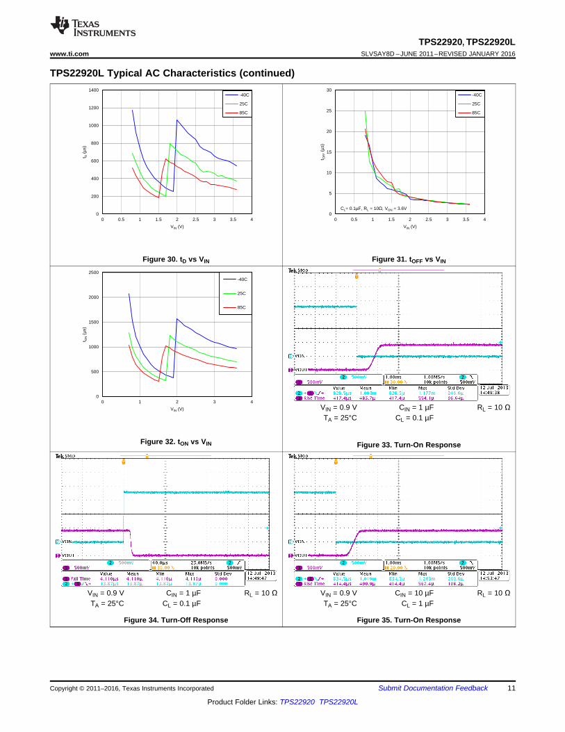
Figure 30. tD vs VIN Figure 31. tOFF vs VIN
Figure 32. tON vs VIN
VIN = 0.9 V CIN = 1 µF RL = 10 ΩTA = 25°C CL = 0.1 µF
Figure 33. Turn-On Response
VIN = 0.9 V CIN = 1 µF RL = 10 ΩTA = 25°C CL = 0.1 µF
Figure 34. Turn-Off Response
VIN = 0.9 V CIN = 10 µF RL = 10 ΩTA = 25°C CL = 1 µF
Figure 35. Turn-On Response
12
TPS22920, TPS22920LSLVSAY8D –JUNE 2011–REVISED JANUARY 2016 www.ti.com
Product Folder Links: TPS22920 TPS22920L
Submit Documentation Feedback Copyright © 2011–2016, Texas Instruments Incorporated
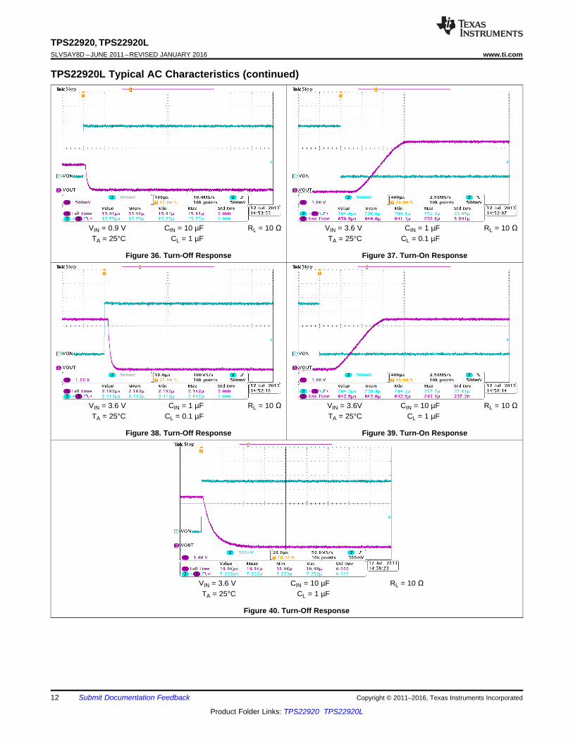
TPS22920L Typical AC Characteristics (continued)
VIN = 0.9 V CIN = 10 µF RL = 10 ΩTA = 25°C CL = 1 µF
Figure 36. Turn-Off Response
VIN = 3.6 V CIN = 1 µF RL = 10 ΩTA = 25°C CL = 0.1 µF
Figure 37. Turn-On Response
VIN = 3.6 V CIN = 1 µF RL = 10 ΩTA = 25°C CL = 0.1 µF
Figure 38. Turn-Off Response
VIN = 3.6V CIN = 10 µF RL = 10 ΩTA = 25°C CL = 1 µF
Figure 39. Turn-On Response
VIN = 3.6 V CIN = 10 µF RL = 10 ΩTA = 25°C CL = 1 µF
Figure 40. Turn-Off Response
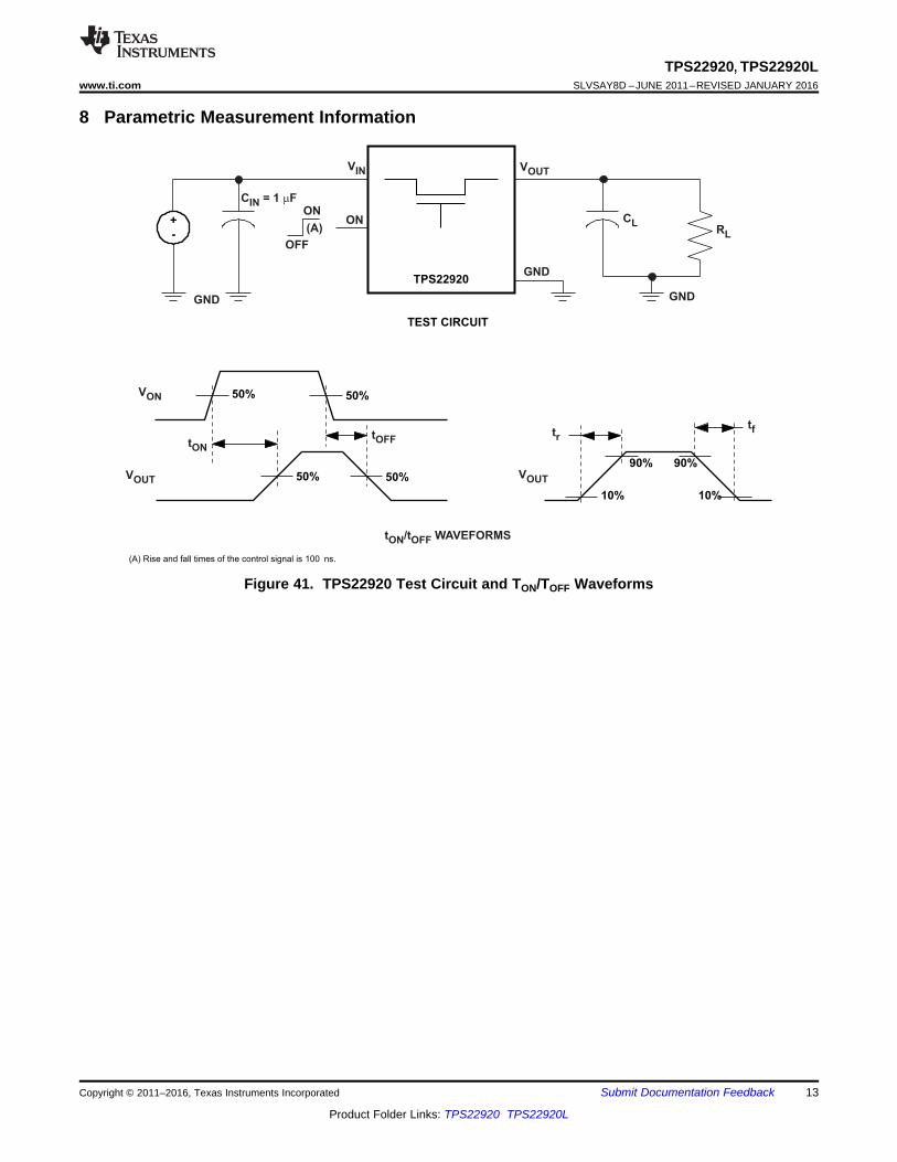
TEST CIRCUIT
+
-
TPS22920
GND
C = 1 FIN m
ON
OFF
(A)ON
VIN
GND
VOUT
CL
GND
RL
(A) Rise and fall times of the control signal is 100 ns.
t /t WAVEFORMSON OFF
90% 90%
10% 10%
50%VON
VOUT
tON
50%
tOFF
50% 50% VOUT
trtf
13
TPS22920, TPS22920Lwww.ti.com SLVSAY8D –JUNE 2011–REVISED JANUARY 2016
Product Folder Links: TPS22920 TPS22920L
Submit Documentation FeedbackCopyright © 2011–2016, Texas Instruments Incorporated
8 Parametric Measurement Information
Figure 41. TPS22920 Test Circuit and TON/TOFF Waveforms
+
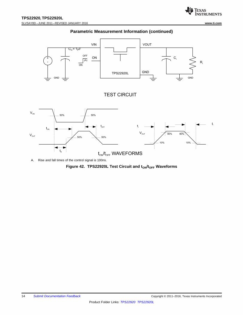
-ON
OFF
TPS22920L
VIN VOUT
RL
CL
TEST CIRCUIT
GND
(A)
GND
tr
tf
tON
tOFF
90% 90%
10% 10%
t /t WAVEFORMSON OFF
VON
VOUT
VOUT
ON
GND
50% 50%
50% 50%
C = 1IN µF
tD
14
TPS22920, TPS22920LSLVSAY8D –JUNE 2011–REVISED JANUARY 2016 www.ti.com
Product Folder Links: TPS22920 TPS22920L
Submit Documentation Feedback Copyright © 2011–2016, Texas Instruments Incorporated
Parametric Measurement Information (continued)
A. Rise and fall times of the control signal is 100ns.
Figure 42. TPS22920L Test Circuit and tON/tOFF Waveforms
Charge
Pump
Control
Logic
GND
VIN
ON
VOUT
15
TPS22920, TPS22920Lwww.ti.com SLVSAY8D –JUNE 2011–REVISED JANUARY 2016
Product Folder Links: TPS22920 TPS22920L
Submit Documentation FeedbackCopyright © 2011–2016, Texas Instruments Incorporated
(1) See Output Pull-Down .
9 Detailed Description
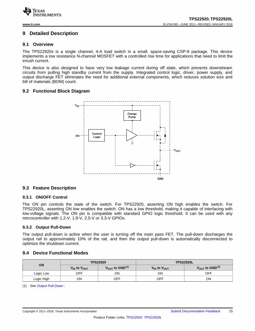
9.1 OverviewThe TPS22920x is a single channel, 4-A load switch in a small, space-saving CSP-8 package. This deviceimplements a low resistance N-channel MOSFET with a controlled rise time for applications that need to limit theinrush current.
This device is also designed to have very low leakage current during off state, which prevents downstreamcircuits from pulling high standby current from the supply. Integrated control logic, driver, power supply, andoutput discharge FET eliminates the need for additional external components, which reduces solution size andbill of materials (BOM) count.
9.2 Functional Block Diagram
9.3 Feature Description
9.3.1 ON/OFF ControlThe ON pin controls the state of the switch. For TPS22920, asserting ON high enables the switch. ForTPS22920L, asserting ON low enables the switch. ON has a low threshold, making it capable of interfacing withlow-voltage signals. The ON pin is compatible with standard GPIO logic threshold. It can be used with anymicrocontroller with 1.2-V, 1.8-V, 2.5-V or 3.3-V GPIOs.
9.3.2 Output Pull-DownThe output pull-down is active when the user is turning off the main pass FET. The pull-down discharges theoutput rail to approximately 10% of the rail, and then the output pull-down is automatically disconnected tooptimize the shutdown current.
9.4 Device Functional Modes
ONTPS22920 TPS22920L
VIN to VOUT VOUT to GND (1) VIN to VOUT VOUT to GND (1)
Logic Low OFF ON ON OFFLogic High ON OFF OFF ON
SMPS
OFF
ON
TPS22920
VOUT
RL
CL
GND
ON
GND
CIN
VIN
16
TPS22920, TPS22920LSLVSAY8D –JUNE 2011–REVISED JANUARY 2016 www.ti.com
Product Folder Links: TPS22920 TPS22920L
Submit Documentation Feedback Copyright © 2011–2016, Texas Instruments Incorporated
10 Application and Implementation
NOTEInformation in the following applications sections is not part of the TI componentspecification, and TI does not warrant its accuracy or completeness. TI’s customers areresponsible for determining suitability of components for their purposes. Customers shouldvalidate and test their design implementation to confirm system functionality.
10.1 Application Information
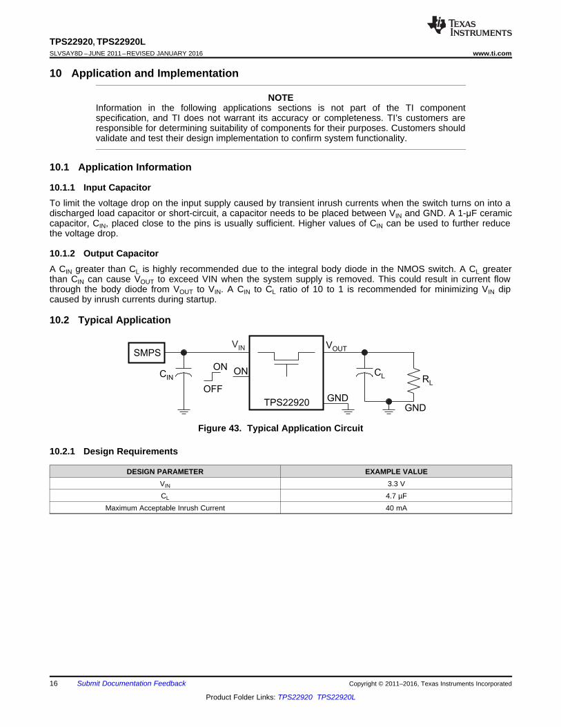
10.1.1 Input CapacitorTo limit the voltage drop on the input supply caused by transient inrush currents when the switch turns on into adischarged load capacitor or short-circuit, a capacitor needs to be placed between VIN and GND. A 1-μF ceramiccapacitor, CIN, placed close to the pins is usually sufficient. Higher values of CIN can be used to further reducethe voltage drop.
10.1.2 Output CapacitorA CIN greater than CL is highly recommended due to the integral body diode in the NMOS switch. A CL greaterthan CIN can cause VOUT to exceed VIN when the system supply is removed. This could result in current flowthrough the body diode from VOUT to VIN. A CIN to CL ratio of 10 to 1 is recommended for minimizing VIN dipcaused by inrush currents during startup.
10.2 Typical Application
Figure 43. Typical Application Circuit
10.2.1 Design Requirements
DESIGN PARAMETER EXAMPLE VALUEVIN 3.3 VCL 4.7 µF
Maximum Acceptable Inrush Current 40 mA
dv8.5V/ms
dt=
dv40mA 4.7 F
dt= m ´
dvOutput slew rate
dt=
dvInrush Current C
dt= ´
17
TPS22920, TPS22920Lwww.ti.com SLVSAY8D –JUNE 2011–REVISED JANUARY 2016
Product Folder Links: TPS22920 TPS22920L
Submit Documentation FeedbackCopyright © 2011–2016, Texas Instruments Incorporated
10.2.2 Detailed Design Procedure
10.2.2.1 VIN to VOUT Voltage DropThe VIN to VOUT voltage drop in the device is determined by the RON of the device and the load current. TheRON of the device depends upon the VIN condition of the device. Refer to the RON specification of the device inthe Electrical Characteristics table of this datasheet. Once the RON of the device is determined based upon theVIN conditions, use Equation 1 to calculate the VIN to VOUT voltage drop:
ΔV = ILOAD × RON
where• ΔV = Voltage drop from VIN to VOUT• ILOAD = Load current• RON = On-resistance of the device for a specific VIN
• An appropriate ILOAD must be chosen such that the IMAX specification of the device is not violated. (1)
10.2.2.2 Managing Inrush CurrentThe output capacitors must be charged up from 0-V to VIN when the switch is enabled. This charge arrives in theform of inrush current. Inrush current may be calculated using the following equation:
where• C = Output capacitance
• (2)
The TPS22920x offers a very slow controlled rise time for minimizing inrush current. This device can be selectedbased upon the maximum acceptable slew rate which can be calculated using the design requirements and theinrush current equation. An output capacitance of 4.7 μF will be used since the amount of inrush increases withoutput capacitance:
(3)
(4)
A device with a slew rate less than 8.5 V/ms must be used to ensure an inrush current of less than 40 mA.
The TPS22920 has a typical rise time of 880 μs at 3.3 V. This results in a slew rate of 3.75 V/ms which meetsthe Design Requirements.
18
TPS22920, TPS22920LSLVSAY8D –JUNE 2011–REVISED JANUARY 2016 www.ti.com
Product Folder Links: TPS22920 TPS22920L
Submit Documentation Feedback Copyright © 2011–2016, Texas Instruments Incorporated
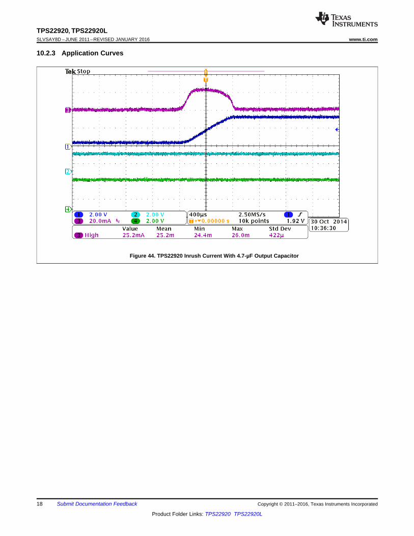
10.2.3 Application Curves
Figure 44. TPS22920 Inrush Current With 4.7-µF Output Capacitor
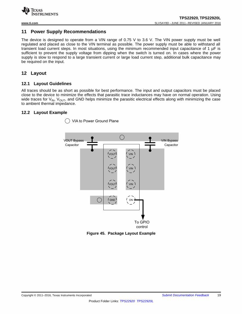
VIA to Power Ground Plane
VOUT Bypass
Capacitor
To GPIO
control
VIN Bypass
Capacitor
VOUT
VOUT
GND
VIN
VIN
ON
VOUT VIN
19
TPS22920, TPS22920Lwww.ti.com SLVSAY8D –JUNE 2011–REVISED JANUARY 2016
Product Folder Links: TPS22920 TPS22920L
Submit Documentation FeedbackCopyright © 2011–2016, Texas Instruments Incorporated
11 Power Supply RecommendationsThe device is designed to operate from a VIN range of 0.75 V to 3.6 V. The VIN power supply must be wellregulated and placed as close to the VIN terminal as possible. The power supply must be able to withstand alltransient load current steps. In most situations, using the minimum recommended input capacitance of 1 µF issufficient to prevent the supply voltage from dipping when the switch is turned on. In cases where the powersupply is slow to respond to a large transient current or large load current step, additional bulk capacitance maybe required on the input.
12 Layout
12.1 Layout GuidelinesAll traces should be as short as possible for best performance. The input and output capacitors must be placedclose to the device to minimize the effects that parasitic trace inductances may have on normal operation. Usingwide traces for VIN, VOUT, and GND helps minimize the parasitic electrical effects along with minimizing the caseto ambient thermal impedance.
12.2 Layout Example
Figure 45. Package Layout Example
20
TPS22920, TPS22920LSLVSAY8D –JUNE 2011–REVISED JANUARY 2016 www.ti.com
Product Folder Links: TPS22920 TPS22920L
Submit Documentation Feedback Copyright © 2011–2016, Texas Instruments Incorporated
13 Device and Documentation Support
13.1 Related LinksThe table below lists quick access links. Categories include technical documents, support and communityresources, tools and software, and quick access to sample or buy.
Table 2. Related Links
PARTS PRODUCT FOLDER SAMPLE & BUY TECHNICALDOCUMENTS
TOOLS &SOFTWARE
SUPPORT &COMMUNITY
TPS22920 Click here Click here Click here Click here Click hereTPS22920L Click here Click here Click here Click here Click here
13.2 TrademarksAll trademarks are the property of their respective owners.
13.3 Electrostatic Discharge CautionThese devices have limited built-in ESD protection. The leads should be shorted together or the device placed in conductive foamduring storage or handling to prevent electrostatic damage to the MOS gates.
13.4 GlossarySLYZ022 — TI Glossary.
This glossary lists and explains terms, acronyms, and definitions.
14 Mechanical, Packaging, and Orderable InformationThe following pages include mechanical, packaging, and orderable information. This information is the mostcurrent data available for the designated devices. This data is subject to change without notice and revision ofthis document. For browser-based versions of this data sheet, refer to the left-hand navigation.
PACKAGE OPTION ADDENDUM
www.ti.com 19-Jan-2016
Addendum-Page 1
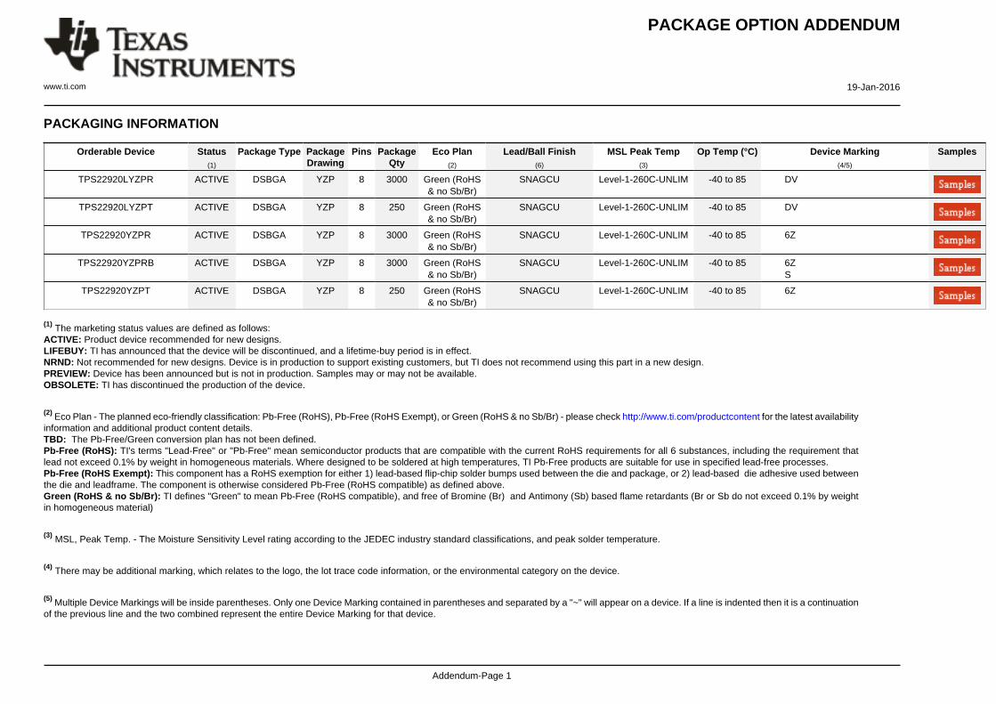
PACKAGING INFORMATION
Orderable Device Status(1)
Package Type PackageDrawing
Pins PackageQty
Eco Plan(2)
Lead/Ball Finish(6)
MSL Peak Temp(3)
Op Temp (°C) Device Marking(4/5)
Samples
TPS22920LYZPR ACTIVE DSBGA YZP 8 3000 Green (RoHS& no Sb/Br)
SNAGCU Level-1-260C-UNLIM -40 to 85 DV
TPS22920LYZPT ACTIVE DSBGA YZP 8 250 Green (RoHS& no Sb/Br)
SNAGCU Level-1-260C-UNLIM -40 to 85 DV
TPS22920YZPR ACTIVE DSBGA YZP 8 3000 Green (RoHS& no Sb/Br)
SNAGCU Level-1-260C-UNLIM -40 to 85 6Z
TPS22920YZPRB ACTIVE DSBGA YZP 8 3000 Green (RoHS& no Sb/Br)
SNAGCU Level-1-260C-UNLIM -40 to 85 6ZS
TPS22920YZPT ACTIVE DSBGA YZP 8 250 Green (RoHS& no Sb/Br)
SNAGCU Level-1-260C-UNLIM -40 to 85 6Z
(1) The marketing status values are defined as follows:ACTIVE: Product device recommended for new designs.LIFEBUY: TI has announced that the device will be discontinued, and a lifetime-buy period is in effect.NRND: Not recommended for new designs. Device is in production to support existing customers, but TI does not recommend using this part in a new design.PREVIEW: Device has been announced but is not in production. Samples may or may not be available.OBSOLETE: TI has discontinued the production of the device.
(2) Eco Plan - The planned eco-friendly classification: Pb-Free (RoHS), Pb-Free (RoHS Exempt), or Green (RoHS & no Sb/Br) - please check http://www.ti.com/productcontent for the latest availabilityinformation and additional product content details.TBD: The Pb-Free/Green conversion plan has not been defined.Pb-Free (RoHS): TI's terms "Lead-Free" or "Pb-Free" mean semiconductor products that are compatible with the current RoHS requirements for all 6 substances, including the requirement thatlead not exceed 0.1% by weight in homogeneous materials. Where designed to be soldered at high temperatures, TI Pb-Free products are suitable for use in specified lead-free processes.Pb-Free (RoHS Exempt): This component has a RoHS exemption for either 1) lead-based flip-chip solder bumps used between the die and package, or 2) lead-based die adhesive used betweenthe die and leadframe. The component is otherwise considered Pb-Free (RoHS compatible) as defined above.Green (RoHS & no Sb/Br): TI defines "Green" to mean Pb-Free (RoHS compatible), and free of Bromine (Br) and Antimony (Sb) based flame retardants (Br or Sb do not exceed 0.1% by weightin homogeneous material)
(3) MSL, Peak Temp. - The Moisture Sensitivity Level rating according to the JEDEC industry standard classifications, and peak solder temperature.
(4) There may be additional marking, which relates to the logo, the lot trace code information, or the environmental category on the device.
(5) Multiple Device Markings will be inside parentheses. Only one Device Marking contained in parentheses and separated by a "~" will appear on a device. If a line is indented then it is a continuationof the previous line and the two combined represent the entire Device Marking for that device.
PACKAGE OPTION ADDENDUM
www.ti.com 19-Jan-2016
Addendum-Page 2
(6) Lead/Ball Finish - Orderable Devices may have multiple material finish options. Finish options are separated by a vertical ruled line. Lead/Ball Finish values may wrap to two lines if the finishvalue exceeds the maximum column width.
Important Information and Disclaimer:The information provided on this page represents TI's knowledge and belief as of the date that it is provided. TI bases its knowledge and belief on informationprovided by third parties, and makes no representation or warranty as to the accuracy of such information. Efforts are underway to better integrate information from third parties. TI has taken andcontinues to take reasonable steps to provide representative and accurate information but may not have conducted destructive testing or chemical analysis on incoming materials and chemicals.TI and TI suppliers consider certain information to be proprietary, and thus CAS numbers and other limited information may not be available for release.
In no event shall TI's liability arising out of such information exceed the total purchase price of the TI part(s) at issue in this document sold by TI to Customer on an annual basis.
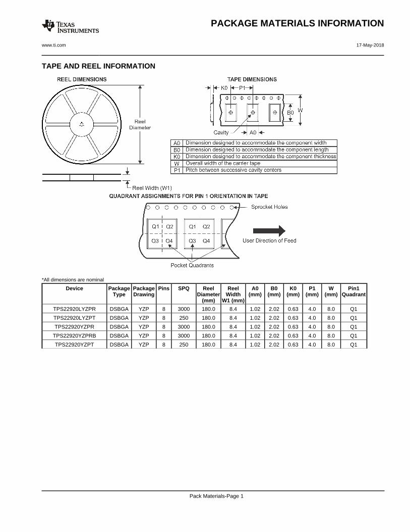
TAPE AND REEL INFORMATION
*All dimensions are nominal
Device PackageType
PackageDrawing
Pins SPQ ReelDiameter
(mm)
ReelWidth
W1 (mm)
A0(mm)
B0(mm)
K0(mm)
P1(mm)
W(mm)
Pin1Quadrant
TPS22920LYZPR DSBGA YZP 8 3000 180.0 8.4 1.02 2.02 0.63 4.0 8.0 Q1
TPS22920LYZPT DSBGA YZP 8 250 180.0 8.4 1.02 2.02 0.63 4.0 8.0 Q1
TPS22920YZPR DSBGA YZP 8 3000 180.0 8.4 1.02 2.02 0.63 4.0 8.0 Q1
TPS22920YZPRB DSBGA YZP 8 3000 180.0 8.4 1.02 2.02 0.63 4.0 8.0 Q1
TPS22920YZPT DSBGA YZP 8 250 180.0 8.4 1.02 2.02 0.63 4.0 8.0 Q1
PACKAGE MATERIALS INFORMATION
www.ti.com 17-May-2018
Pack Materials-Page 1
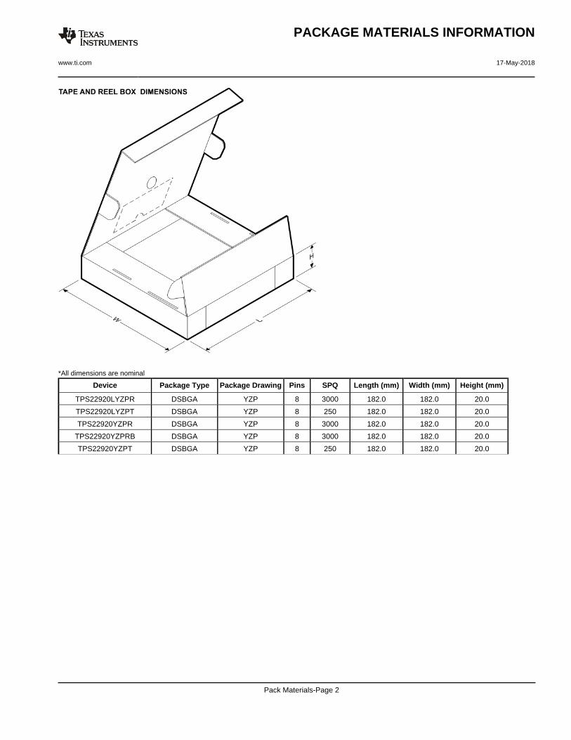
*All dimensions are nominal
Device Package Type Package Drawing Pins SPQ Length (mm) Width (mm) Height (mm)
TPS22920LYZPR DSBGA YZP 8 3000 182.0 182.0 20.0
TPS22920LYZPT DSBGA YZP 8 250 182.0 182.0 20.0
TPS22920YZPR DSBGA YZP 8 3000 182.0 182.0 20.0
TPS22920YZPRB DSBGA YZP 8 3000 182.0 182.0 20.0
TPS22920YZPT DSBGA YZP 8 250 182.0 182.0 20.0
PACKAGE MATERIALS INFORMATION
www.ti.com 17-May-2018
Pack Materials-Page 2
www.ti.com
PACKAGE OUTLINE
C0.5 MAX
0.190.15
1.5TYP
0.5 TYP
8X 0.250.21
0.5TYP
B E A
D
4223082/A 07/2016
DSBGA - 0.5 mm max heightYZP0008DIE SIZE BALL GRID ARRAY
NOTES: 1. All linear dimensions are in millimeters. Any dimensions in parenthesis are for reference only. Dimensioning and tolerancing per ASME Y14.5M.2. This drawing is subject to change without notice.
BALL A1CORNER
SEATING PLANE
BALL TYP0.05 C
B
1 2
0.015 C A B
SYMM
SYMM
C
A
D
SCALE 8.000
D: Max =
E: Max =
1.934 mm, Min =
0.934 mm, Min =
1.874 mm
0.874 mm
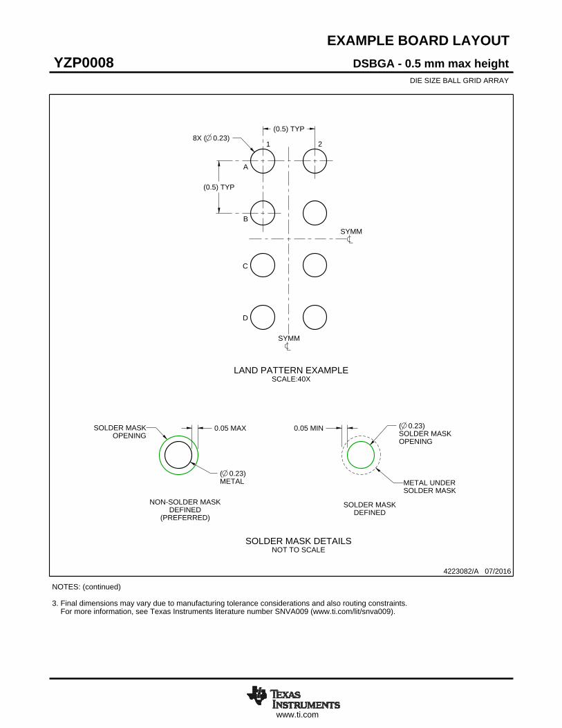
www.ti.com
EXAMPLE BOARD LAYOUT
8X ( 0.23)(0.5) TYP
(0.5) TYP
( 0.23)METAL
0.05 MAX ( 0.23)SOLDER MASKOPENING
0.05 MIN
4223082/A 07/2016
DSBGA - 0.5 mm max heightYZP0008DIE SIZE BALL GRID ARRAY
NOTES: (continued) 3. Final dimensions may vary due to manufacturing tolerance considerations and also routing constraints. For more information, see Texas Instruments literature number SNVA009 (www.ti.com/lit/snva009).
SYMM
SYMM
LAND PATTERN EXAMPLESCALE:40X
1 2
A
B
C
D
NON-SOLDER MASKDEFINED
(PREFERRED)
SOLDER MASK DETAILSNOT TO SCALE
SOLDER MASKOPENING
SOLDER MASKDEFINED
METAL UNDERSOLDER MASK
www.ti.com
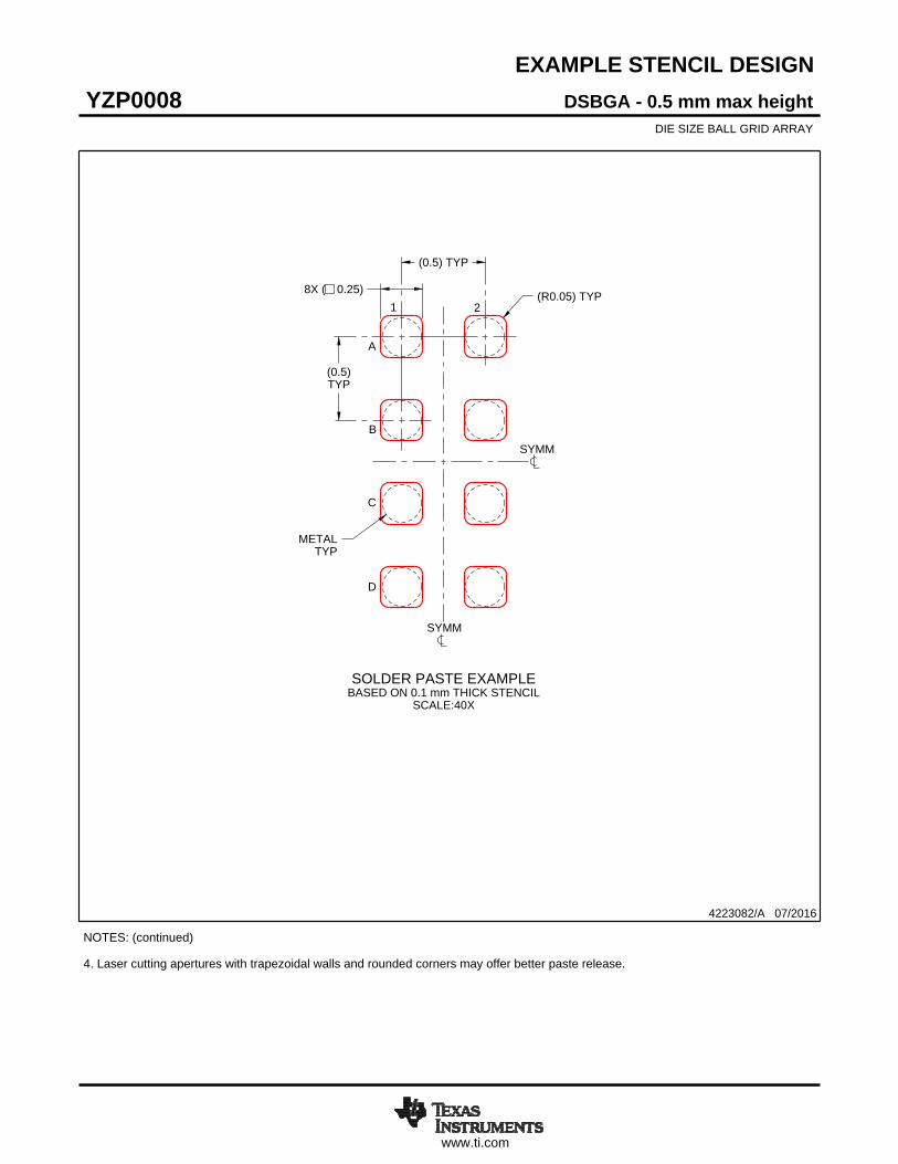
EXAMPLE STENCIL DESIGN
(0.5)TYP
(0.5) TYP
8X ( 0.25) (R0.05) TYP
METALTYP
4223082/A 07/2016
DSBGA - 0.5 mm max heightYZP0008DIE SIZE BALL GRID ARRAY
NOTES: (continued) 4. Laser cutting apertures with trapezoidal walls and rounded corners may offer better paste release.
SYMM
SYMM
SOLDER PASTE EXAMPLEBASED ON 0.1 mm THICK STENCIL
SCALE:40X
1 2
A
B
C
D
IMPORTANT NOTICE
Texas Instruments Incorporated (TI) reserves the right to make corrections, enhancements, improvements and other changes to itssemiconductor products and services per JESD46, latest issue, and to discontinue any product or service per JESD48, latest issue. Buyersshould obtain the latest relevant information before placing orders and should verify that such information is current and complete.TI’s published terms of sale for semiconductor products (http://www.ti.com/sc/docs/stdterms.htm) apply to the sale of packaged integratedcircuit products that TI has qualified and released to market. Additional terms may apply to the use or sale of other types of TI products andservices.Reproduction of significant portions of TI information in TI data sheets is permissible only if reproduction is without alteration and isaccompanied by all associated warranties, conditions, limitations, and notices. TI is not responsible or liable for such reproduceddocumentation. Information of third parties may be subject to additional restrictions. Resale of TI products or services with statementsdifferent from or beyond the parameters stated by TI for that product or service voids all express and any implied warranties for theassociated TI product or service and is an unfair and deceptive business practice. TI is not responsible or liable for any such statements.Buyers and others who are developing systems that incorporate TI products (collectively, “Designers”) understand and agree that Designersremain responsible for using their independent analysis, evaluation and judgment in designing their applications and that Designers havefull and exclusive responsibility to assure the safety of Designers' applications and compliance of their applications (and of all TI productsused in or for Designers’ applications) with all applicable regulations, laws and other applicable requirements. Designer represents that, withrespect to their applications, Designer has all the necessary expertise to create and implement safeguards that (1) anticipate dangerousconsequences of failures, (2) monitor failures and their consequences, and (3) lessen the likelihood of failures that might cause harm andtake appropriate actions. Designer agrees that prior to using or distributing any applications that include TI products, Designer willthoroughly test such applications and the functionality of such TI products as used in such applications.TI’s provision of technical, application or other design advice, quality characterization, reliability data or other services or information,including, but not limited to, reference designs and materials relating to evaluation modules, (collectively, “TI Resources”) are intended toassist designers who are developing applications that incorporate TI products; by downloading, accessing or using TI Resources in anyway, Designer (individually or, if Designer is acting on behalf of a company, Designer’s company) agrees to use any particular TI Resourcesolely for this purpose and subject to the terms of this Notice.TI’s provision of TI Resources does not expand or otherwise alter TI’s applicable published warranties or warranty disclaimers for TIproducts, and no additional obligations or liabilities arise from TI providing such TI Resources. TI reserves the right to make corrections,enhancements, improvements and other changes to its TI Resources. TI has not conducted any testing other than that specificallydescribed in the published documentation for a particular TI Resource.Designer is authorized to use, copy and modify any individual TI Resource only in connection with the development of applications thatinclude the TI product(s) identified in such TI Resource. NO OTHER LICENSE, EXPRESS OR IMPLIED, BY ESTOPPEL OR OTHERWISETO ANY OTHER TI INTELLECTUAL PROPERTY RIGHT, AND NO LICENSE TO ANY TECHNOLOGY OR INTELLECTUAL PROPERTYRIGHT OF TI OR ANY THIRD PARTY IS GRANTED HEREIN, including but not limited to any patent right, copyright, mask work right, orother intellectual property right relating to any combination, machine, or process in which TI products or services are used. Informationregarding or referencing third-party products or services does not constitute a license to use such products or services, or a warranty orendorsement thereof. Use of TI Resources may require a license from a third party under the patents or other intellectual property of thethird party, or a license from TI under the patents or other intellectual property of TI.TI RESOURCES ARE PROVIDED “AS IS” AND WITH ALL FAULTS. TI DISCLAIMS ALL OTHER WARRANTIES ORREPRESENTATIONS, EXPRESS OR IMPLIED, REGARDING RESOURCES OR USE THEREOF, INCLUDING BUT NOT LIMITED TOACCURACY OR COMPLETENESS, TITLE, ANY EPIDEMIC FAILURE WARRANTY AND ANY IMPLIED WARRANTIES OFMERCHANTABILITY, FITNESS FOR A PARTICULAR PURPOSE, AND NON-INFRINGEMENT OF ANY THIRD PARTY INTELLECTUALPROPERTY RIGHTS. TI SHALL NOT BE LIABLE FOR AND SHALL NOT DEFEND OR INDEMNIFY DESIGNER AGAINST ANY CLAIM,INCLUDING BUT NOT LIMITED TO ANY INFRINGEMENT CLAIM THAT RELATES TO OR IS BASED ON ANY COMBINATION OFPRODUCTS EVEN IF DESCRIBED IN TI RESOURCES OR OTHERWISE. IN NO EVENT SHALL TI BE LIABLE FOR ANY ACTUAL,DIRECT, SPECIAL, COLLATERAL, INDIRECT, PUNITIVE, INCIDENTAL, CONSEQUENTIAL OR EXEMPLARY DAMAGES INCONNECTION WITH OR ARISING OUT OF TI RESOURCES OR USE THEREOF, AND REGARDLESS OF WHETHER TI HAS BEENADVISED OF THE POSSIBILITY OF SUCH DAMAGES.Unless TI has explicitly designated an individual product as meeting the requirements of a particular industry standard (e.g., ISO/TS 16949and ISO 26262), TI is not responsible for any failure to meet such industry standard requirements.Where TI specifically promotes products as facilitating functional safety or as compliant with industry functional safety standards, suchproducts are intended to help enable customers to design and create their own applications that meet applicable functional safety standardsand requirements. Using products in an application does not by itself establish any safety features in the application. Designers mustensure compliance with safety-related requirements and standards applicable to their applications. Designer may not use any TI products inlife-critical medical equipment unless authorized officers of the parties have executed a special contract specifically governing such use.Life-critical medical equipment is medical equipment where failure of such equipment would cause serious bodily injury or death (e.g., lifesupport, pacemakers, defibrillators, heart pumps, neurostimulators, and implantables). Such equipment includes, without limitation, allmedical devices identified by the U.S. Food and Drug Administration as Class III devices and equivalent classifications outside the U.S.TI may expressly designate certain products as completing a particular qualification (e.g., Q100, Military Grade, or Enhanced Product).Designers agree that it has the necessary expertise to select the product with the appropriate qualification designation for their applicationsand that proper product selection is at Designers’ own risk. Designers are solely responsible for compliance with all legal and regulatoryrequirements in connection with such selection.Designer will fully indemnify TI and its representatives against any damages, costs, losses, and/or liabilities arising out of Designer’s non-compliance with the terms and provisions of this Notice.
Mailing Address: Texas Instruments, Post Office Box 655303, Dallas, Texas 75265Copyright © 2018, Texas Instruments Incorporated