Embed Size (px)
Citation preview

1. General description
NXP’s UCODE 7 IC is the leading-edge EPC Gen2 RFID chip that offers best-in-class performance and features for use in the most demanding RFID tagging applications.
Particularly well suited for inventory management application, like e.g Retail and Fashion, with its leading edge RF performance for any given form factor, UCODE 7 enables long read distance and fast inventory of dense RFID tag population. With its broadband design, it offers the possibility to manufacture true global RFID label with best-in-class performance over worldwide regulations.
The device also provides a pre-serialized 96-bit EPC and a Parallel encoding feature. For applications where the same 58-bit Stock Keeping Unit (SKU) needs to be encoded on multiple tags, at the same time, a combination of both features improves and simplifies the tag initialization process.
On top UCODE 7 offers a Tag Power Indicator for RFID tag initialization optimization and a Product Status Flag for Electronic Article Surveillance (EAS) application.
2. Features and benefits
2.1 Key features
Read sensitivity 21 dBm
Write sensitivity 16 dBm
Parallel encoding mode: 100 items in 60ms
Encoding speed: 16 bits per millisecond
Innovative functionalities
Tag Power Indicator
Pre-serialization for 96-bit EPC
Integrated Product Status Flag (PSF)
Compatible with single-slit antenna
Up to 128-bit EPC
96-bit Unique Tag Identifier (TID) factory locked,including 48-bit unique serial number
EPC Gen2 v2.0 ready
SL3S1204UCODE 7Rev. 3.9 — 21 March 2017241339
Product data sheetCOMPANY PUBLIC

NXP Semiconductors SL3S1204UCODE 7
2.1.1 Memory
Up to 128-bit of EPC memory
Supports pre-serialization for 96-bit EPC
96-bit Tag IDentifier (TID) factory locked
48-bit unique serial number factory-encoded into TID
No User Memory
32-bit kill password to permanently disable the tag
32-bit access password
Wide operating temperature range: 40 C up to +85 C Minimum 100.000 write cycle endurance
2.2 Key benefits
2.2.1 End user benefit
Long READ and WRITE ranges due to leading edge chip sensitivity
Very fast bulk encoding
Product identification through unalterable extended TID range, including a 48-bit serial number
Reliable operation in dense reader and noisy environments through high interference rejection
2.2.2 Antenna design benefits
High sensitivity enables smaller and cost efficient antenna designs for the same retail category
Tag Power Indicator features enables very high density of inlay on rolls without cross- talk issues during writing/encoding
The different input capacitance for the single slit antenna solution provides an additional possibility in tuning of the impedance for the antenna design
2.2.3 Label manufacturer benefit
Large RF pad-to-pad distance to ease antenna design
Symmetric RF inputs are less sensitive to process variation
Single slit antenna for a more mechanically stable antenna connection
Pre-serialization of the 96-bit EPC
Extremely fast encoding of the EPC content
2.3 Supported features
All mandatory commands of EPC global specification V.1.2.0 are implemented including:
(Perma)LOCK
Kill Command
The following optional commands are implemented in conformance with the EPC specification:
Access
BlockWrite (2 words, 32-bit)
SL3S1204 All information provided in this document is subject to legal disclaimers. © NXP Semiconductors N.V. 2017. All rights reserved.
Product data sheetCOMPANY PUBLIC
Rev. 3.9 — 21 March 2017241339 2 of 34

NXP Semiconductors SL3S1204UCODE 7
Product Status Flag bit: enables the UHF RFID tag to be used as EAS
(Electronic Article Surveillance) tag without the need for a back-end data base.
Tag Power Indicator: enables the reader to select only ICs/tags that have enough power to be written to.
Parallel encoding: allows for the ability to bring (multiple) tag(s) quickly to the OPEN state and hence allowing single tags to be identified simply, without timing restrictions, or multiple tags to be e.g. written to at the same time, considerably reducing the encoding process
All supported features of UCODE 7 can be activated using standard EPCglobal READ / WRITE / ACCESS / SELECT commands. No custom commands are needed to take advantage of all the features in case of unlocked EPC memory. The parallel encoding feature may however require a firmware upgrade of the reader to use its full potential.
3. Applications
3.1 Markets
Retail/Fashion (apparel, footwear, jewelry, cosmetics)
Fast Moving Consumer Goods
3.2 Applications
Retail Inventory management
Supply chain management
Loss prevention
Asset management
Outside the applications mentioned above, please contact NXP Semiconductors for support.
4. Ordering information
Table 1. Ordering information
Type number Package
Name IC type Description Version
SL3S1204FUD/BG1 Wafer UCODE 7 bumped die on sawn 8” 120 m wafer 7 m Polyimide spacer
not applicable
SL3S1204FUD/HA1 Wafer UCODE 7 die with large pads 3 m Au, 10 m Polyimide spacer on sawn 8” 120 m wafer
not applicable
SL3S1204FUD2/BG1 Wafer UCODE 7 bumped die on sawn 12” 120 m wafer 7 m Polyimide spacer
not applicable
SL3S1204FTB0/1 XSON6 UCODE 7 plastic extremely thin small outline package; no leads; 6 terminals; body 1 1.45 0.5 mm
SOT886F1
SL3S1204 All information provided in this document is subject to legal disclaimers. © NXP Semiconductors N.V. 2017. All rights reserved.
Product data sheetCOMPANY PUBLIC
Rev. 3.9 — 21 March 2017241339 3 of 34

NXP Semiconductors SL3S1204UCODE 7
5. Marking
6. Block diagram
The SL3S1204 IC consists of three major blocks:
- Analog Interface
- Digital Control
- EEPROM
The analog part provides stable supply voltage and demodulates data received from the reader which is then processed by the digital part. Further, the modulation transistor of the analog part transmits data back to the reader.
The digital section includes the state machines, processes the protocol and handles communication with the EEPROM, which contains the EPC and the user data.
Table 2. Marking codes
Type number Marking code Comment Version
SL3S1204FTB0/1 YM UCODE 7 SOT886
Fig 1. Block diagram of UCODE 7 IC
aaa-005856
ANALOGRF INTERFACE
VREG
MODdataout
datain
R/W
VDD
DEMODRECT
antenna
RF1
RF2
DIGITAL CONTROL
ANTICOLLISION
READWRITECONTROL
ACCESS CONTROL
EEPROM INTERFACECONTROL
RF INTERFACECONTROL
SEQUENCERCHARGE PUMP
EEPROM
MEMORY
SL3S1204 All information provided in this document is subject to legal disclaimers. © NXP Semiconductors N.V. 2017. All rights reserved.
Product data sheetCOMPANY PUBLIC
Rev. 3.9 — 21 March 2017241339 4 of 34

NXP Semiconductors SL3S1204UCODE 7
7. Pinning information
7.1 Pin description
Fig 2. Pinning bare die Fig 3. Pin configuration for SOT886
aaa-005611
TP2
TP1 RF2
RF1
SL3S1204 trademarkSL3S12x4FTB0
n.c.
aaa-018831
RF2
n.c.
n.c.
RF1
n.c.
Transparent top view
2
3
1
5
4
6
Table 3. Pin description bare die
Symbol Description
TP1 test pad 1
RF1 antenna connector 1
TP2 test pad 2
RF2 antenna connector 2
Table 4. Pin description SOT886
Pin Symbol Description
1 RF2 antenna connector
2 n.c. not connected
3 n.c. not connected
4 n.c. not connected
5 n.c. not connected
6 RF1 antenna connector
SL3S1204 All information provided in this document is subject to legal disclaimers. © NXP Semiconductors N.V. 2017. All rights reserved.
Product data sheetCOMPANY PUBLIC
Rev. 3.9 — 21 March 2017241339 5 of 34

NXP Semiconductors SL3S1204UCODE 7
8. Wafer layout
8.1 Wafer layout 8 inch
(1) Die to Die distance (metal sealring - metal sealring) 21,4 m, (X-scribe line width: 15 m)
(2) Die to Die distance (metal sealring - metal sealring) 21,4 m, (Y-scribe line width: 15 m)
(3) Chip step, x-length: 460 m
(4) Chip step, y-length: 505 m
(5) Bump to bump distance X (TP1 - RF2): 358 m
(6) Bump to bump distance Y (RF1 - RF2): 403 m
(7) Distance bump to metal sealring X: 40,3m (outer edge - top metal)
(8) Distance bump to metal sealring Y: 40,3 m
Bump size X x Y: 60 m x 60 m
Remark: TP1 and TP2 are electrically disconnected after dicing
Fig 4. UCODE 7 8 inch wafer layout
aaa-005606not to scale!
(1)
(7)
(2)
(8)
(5)
(6) (4)
(3)
Y
X
TP2
TP1 RF2
RF1
SL3S1204 All information provided in this document is subject to legal disclaimers. © NXP Semiconductors N.V. 2017. All rights reserved.
Product data sheetCOMPANY PUBLIC
Rev. 3.9 — 21 March 2017241339 6 of 34

NXP Semiconductors SL3S1204UCODE 7
8.2 Wafer layout 8 inch with large pads
(1) Die to Die distance (metal sealring - metal sealring) 21,4 m, (Y-scribe line width: 15 m)
(2) Die to Die distance (metal sealring - metal sealring) 21,4 m, (X-scribe line width: 15 m)
(3) Chip step, x-length: 460 m
(4) Chip step, y-length: 505 m
(5) Bump to bump distance Y (RF1 - RF2): 115 m
(6) Distance bump to metal sealring X: 23,5 m
(7) Bump size (TP1, TP2) X: 130m
(8) Bump to bump distance X (RF1 - TP2): 50 m
(9) Bump size (RF1, RF2) X: 218m
(10) Distance bump to metal sealring Y: 23,5 m
(11) Bump size (TP1, TP2) Y: 153,1m
(12) Bump size (RF1, RF2) Y: 164m
(13) Distance bump to metal sealring Y: 466,5 m
Remark: TP1 and TP2 are electrically disconnected after dicing
Fig 5. UCODE 7 8 inch wafer layout with large pads
aaa-026778not to scale!
(1)
(10)
(2)
(12)
(4)
(3)
Y
X
TP2
TP1 RF2
RF1
(6)
(7)
(8)
(9)
(5)(13)
(11)
SL3S1204 All information provided in this document is subject to legal disclaimers. © NXP Semiconductors N.V. 2017. All rights reserved.
Product data sheetCOMPANY PUBLIC
Rev. 3.9 — 21 March 2017241339 7 of 34

NXP Semiconductors SL3S1204UCODE 7
8.3 Wafer layout 12 inch
(1) Die to Die distance (metal sealring - metal sealring) 39 m, (X-scribe line width: 35 m)
(2) Die to Die distance (metal sealring - metal sealring) 39 m, (Y-scribe line width: 35 m)
(3) Chip step, x-length: 480 m
(4) Chip step, y-length: 525m
(5) Bump to bump distance X (TP1 - RF2): 358 m
(6) Bump to bump distance Y (RF1 - RF2): 403 m
(7) Distance bump to metal sealring X: 40,3m (outer edge - top metal)
(8) Distance bump to metal sealring Y: 40,3 m
Bump size X x Y: 60 m x 60 m
Remark: TP1 and TP2 are electrically disconnected after dicing
Fig 6. UCODE 7 12 inch wafer layout
aaa-005606not to scale!
(1)
(7)
(2)
(8)
(5)
(6) (4)
(3)
Y
X
TP2
TP1 RF2
RF1
SL3S1204 All information provided in this document is subject to legal disclaimers. © NXP Semiconductors N.V. 2017. All rights reserved.
Product data sheetCOMPANY PUBLIC
Rev. 3.9 — 21 March 2017241339 8 of 34

NXP Semiconductors SL3S1204UCODE 7
9. Mechanical specification
The UCODE 7 wafers are available in 120 m thickness. The 120 m thick wafer is enhanced with 7m /10m Polyimide spacer resulting in less coupling between the antenna and the active circuit, leaving more room for process control (like pressure).
9.1 Wafer specification
9.1.1 8 inch Wafer, Standard bumps
See Ref. 21 “Data sheet - Delivery type description – General specification for 8” wafer on UV-tape with electronic fail die marking, BU-S&C document number: 1093**”.
Table 5. Specifications
Wafer
Designation each wafer is scribed with batch number and wafer number
Diameter 200 mm (8”) unsawn - 205 mm typical sawn on foil
Thickness
SL3S1204FUD/BG 120 m 15 m
Number of pads 4
Pad location non diagonal / placed in chip corners
Distance pad to pad RF1-RF2 403.0 m
Distance pad to pad TP1-RF2 358.0 m
Process CMOS 0.14 m
Batch size 25 wafers
Potential good dies per wafer 126.524
Wafer backside
Material Si
Treatment ground and stress release
Roughness Ra max. 0.5 m, Rt max. 5 m
Chip dimensions
Die size excluding scribe 0.490 mm 0.445 mm = 0.218 mm2
Scribe line width: x-dimension = 15 m
y-dimension = 15 m
Passivation on front
Type Sandwich structure
Material PE-Nitride (on top)
Thickness 1.75 m total thickness of passivation
Polyimide spacer 7 m 1 m
Au bump
Bump material > 99.9 % pure Au
Bump hardness 35 – 80 HV 0.005
Bump shear strength > 70 MPa
Bump height
SL3S1204 All information provided in this document is subject to legal disclaimers. © NXP Semiconductors N.V. 2017. All rights reserved.
Product data sheetCOMPANY PUBLIC
Rev. 3.9 — 21 March 2017241339 9 of 34

NXP Semiconductors SL3S1204UCODE 7
[1] Because of the 7 m spacer, the bump will measure 18 m relative height protruding the spacer.
9.1.2 8 inch Wafer, Large pads
See Ref. 21 “Data sheet - Delivery type description – General specification for 8” wafer on UV-tape with electronic fail die marking, BU-S&C document number: 1093**”.
SL3S1204FUD/BG 25 m[1]
Bump height uniformity
within a die 2 m
– within a wafer 3 m
– wafer to wafer 4 m
Bump flatness 1.5 m
Bump size
– RF1, RF2 60 60 m
– TP1, TP2 60 60 m
Bump size variation 5 m
Table 5. Specifications
Table 6. Specifications
Wafer
Designation each wafer is scribed with batch number and wafer number
Diameter 200 mm (8”) unsawn - 205 mm typical sawn on foil
Thickness
SL3S1204FUD/HA 120 m 15 m
Number of pads 4
Pad location non diagonal / placed in chip corners
Process CMOS 0.14 m
Batch size 25 wafers
Potential good dies per wafer 126.524
Wafer backside
Material Si
Treatment ground and stress release
Roughness Ra max. 0.5 m, Rt max. 5 m
Chip dimensions
Die size excluding scribe 0.490 mm 0.445 mm = 0.218 mm2
Scribe line width: x-dimension = 15 m
y-dimension = 15 m
Passivation on front
Type Sandwich structure
Material PE-Nitride (on top)
Thickness 1.75 m total thickness of passivation
Polyimide spacer 10 m 2 m
SL3S1204 All information provided in this document is subject to legal disclaimers. © NXP Semiconductors N.V. 2017. All rights reserved.
Product data sheetCOMPANY PUBLIC
Rev. 3.9 — 21 March 2017241339 10 of 34
NXP Semiconductors SL3S1204UCODE 7
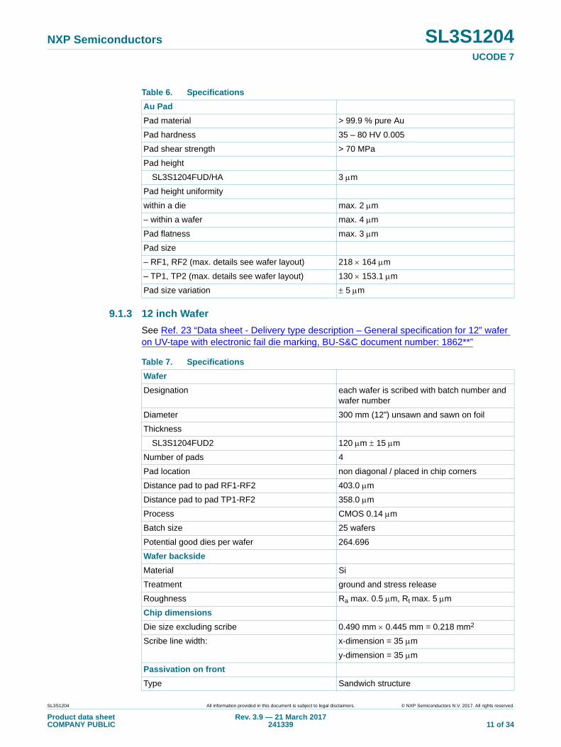
9.1.3 12 inch Wafer
See Ref. 23 “Data sheet - Delivery type description – General specification for 12” wafer on UV-tape with electronic fail die marking, BU-S&C document number: 1862**”
Au Pad
Pad material > 99.9 % pure Au
Pad hardness 35 – 80 HV 0.005
Pad shear strength > 70 MPa
Pad height
SL3S1204FUD/HA 3 m
Pad height uniformity
within a die max. 2 m
– within a wafer max. 4 m
Pad flatness max. 3 m
Pad size
– RF1, RF2 (max. details see wafer layout) 218 164 m
– TP1, TP2 (max. details see wafer layout) 130 153.1 m
Pad size variation 5 m
Table 6. Specifications
Table 7. Specifications
Wafer
Designation each wafer is scribed with batch number and wafer number
Diameter 300 mm (12”) unsawn and sawn on foil
Thickness
SL3S1204FUD2 120 m 15 m
Number of pads 4
Pad location non diagonal / placed in chip corners
Distance pad to pad RF1-RF2 403.0 m
Distance pad to pad TP1-RF2 358.0 m
Process CMOS 0.14 m
Batch size 25 wafers
Potential good dies per wafer 264.696
Wafer backside
Material Si
Treatment ground and stress release
Roughness Ra max. 0.5 m, Rt max. 5 m
Chip dimensions
Die size excluding scribe 0.490 mm 0.445 mm = 0.218 mm2
Scribe line width: x-dimension = 35 m
y-dimension = 35 m
Passivation on front
Type Sandwich structure
SL3S1204 All information provided in this document is subject to legal disclaimers. © NXP Semiconductors N.V. 2017. All rights reserved.
Product data sheetCOMPANY PUBLIC
Rev. 3.9 — 21 March 2017241339 11 of 34

NXP Semiconductors SL3S1204UCODE 7
[1] Because of the 7 m spacer, the bump will measure 18 m relative height protruding the spacer.
9.1.4 Fail die identification
No inkdots are applied to the wafer.
Electronic wafer mapping (SECS II format) covers the electrical test results and additionally the results of mechanical/visual inspection.
See Ref. 21 “Data sheet - Delivery type description – General specification for 8” wafer on UV-tape with electronic fail die marking, BU-S&C document number: 1093**”
See Ref. 23 “Data sheet - Delivery type description – General specification for 12” wafer on UV-tape with electronic fail die marking, BU-S&C document number: 1862**”
9.1.5 Map file distribution
See Ref. 21 “Data sheet - Delivery type description – General specification for 8” wafer on UV-tape with electronic fail die marking, BU-S&C document number: 1093**”
See Ref. 23 “Data sheet - Delivery type description – General specification for 12” wafer on UV-tape with electronic fail die marking, BU-S&C document number: 1862**”
Material PE-Nitride (on top)
Thickness 1.75 m total thickness of passivation
Polyimide spacer 7 m 1 m
Au bump
Bump material > 99.9 % pure Au
Bump hardness 35 – 80 HV 0.005
Bump shear strength > 70 MPa
Bump height
SL3S1204FUD2 25 m[1]
Bump height uniformity
within a die 2 m
– within a wafer 3 m
– wafer to wafer 4 m
Bump flatness 1.5 m
Bump size
– RF1, RF2 60 60 m
– TP1, TP2 60 60 m
Bump size variation 5 m
Table 7. Specifications
SL3S1204 All information provided in this document is subject to legal disclaimers. © NXP Semiconductors N.V. 2017. All rights reserved.
Product data sheetCOMPANY PUBLIC
Rev. 3.9 — 21 March 2017241339 12 of 34

NXP Semiconductors SL3S1204UCODE 7
10. Functional description
10.1 Air interface standards
The UCODE 7 fully supports all parts of the "Specification for RFID Air Interface EPCglobal, EPC Radio-Frequency Identity Protocols, Class-1 Generation-2 UHF RFID, Protocol for Communications at 860 MHz to 960 MHz, Version 1.2.0".
10.2 Power transfer
The interrogator provides an RF field that powers the tag, equipped with a UCODE 7. The antenna transforms the impedance of free space to the chip input impedance in order to get the maximum possible power for the UCODE 7 on the tag.
The RF field, which is oscillating on the operating frequency provided by the interrogator, is rectified to provide a smoothed DC voltage to the analog and digital modules of the IC.
The antenna that is attached to the chip may use a DC connection between the two antenna pads. Therefore the UCODE 7 also enables loop antenna design.
10.3 Data transfer
10.3.1 Interrogator to tag Link
An interrogator transmits information to the UCODE 7 by modulating an UHF RF signal. The UCODE 7 receives both information and operating energy from this RF signal. Tags are passive, meaning that they receive all of their operating energy from the interrogator's RF waveform.
An interrogator is using a fixed modulation and data rate for the duration of at least one inventory round. It communicates to the UCODE 7 by modulating an RF carrier.
For further details refer to Ref. 1. Interrogator-to-tag (R=>T) communications.
10.3.2 Tag to interrogator Link
Upon transmitting a valid command an interrogator receives information from a UCODE 7 tag by transmitting an unmodulated RF carrier and listening for a backscattered reply. The UCODE 7 backscatters by switching the reflection coefficient of its antenna between two states in accordance with the data being sent. For further details refer to Ref. 1, chapter 6.3.1.3.
The UCODE 7 communicates information by backscatter-modulating the amplitude and/or phase of the RF carrier. Interrogators shall be capable of demodulating either demodulation type.
The encoding format, selected in response to interrogator commands, is either FM0 baseband or Miller-modulated subcarrier.
SL3S1204 All information provided in this document is subject to legal disclaimers. © NXP Semiconductors N.V. 2017. All rights reserved.
Product data sheetCOMPANY PUBLIC
Rev. 3.9 — 21 March 2017241339 13 of 34

NXP Semiconductors SL3S1204UCODE 7
10.4 Supported commands
The UCODE 7 supports all mandatory EPCglobal V1.2.0 commands including
• Kill command
• (perma) LOCK command
In addition the UCODE7 supports the following optional commands:
• ACCESS
• Block Write (32 bit)
10.5 UCODE 7 memory
The UCODE 7 memory is implemented according EPCglobal
Class1Gen2 and organized in three banks:
The logical address of all memory banks begin at zero (00h).
In addition to the three memory banks one configuration word to handle the UCODE 7 specific features is available at EPC bank 01 address bit-200h. The configuration word is described in detail in 9.6.
The TID complies to the extended tag Identification scheme according GS1 EPC Tag Data Standard 1.6.
Table 8. UCODE 7 memory sections
Name Size Bank
Reserved memory (32 bit ACCESS and 32 bit KILL password) 64 bit 00b
EPC (excluding 16 bit CRC-16 and 16 bit PC) 128 bit 01b
UCODE 7 Configuration Word 16 bit 01b
TID (including permalocked unique 48 bit serial number) 96 bit 10b
SL3S1204 All information provided in this document is subject to legal disclaimers. © NXP Semiconductors N.V. 2017. All rights reserved.
Product data sheetCOMPANY PUBLIC
Rev. 3.9 — 21 March 2017241339 14 of 34

NXP Semiconductors SL3S1204UCODE 7
10.5.1 UCODE 7 overall memory map
[1] HEX E280 6890 0000 nnnn nnnn nnnn
where n are the nibbles of the SNR from the TID
[2] Indicates the existence of a Configuration Word at the end of the EPC number
[3] See Figure 7
[4] Action bits: meant to trigger a feature upon a SELECT command on the related bit ref feature control mechanism, seeSection 10.6.1
[5] Permanent bit: permanently stored bits in the memory; Read/Writeable according EPC bank lock status, see Section 10.6.1
Table 9. UCODE 7 overall memory map
Bank address
Memory address
Type Content Initial Remark
Bank 00 00h to 1Fh reserved kill password all 00h unlocked memory
20h to 3Fh reserved access password all 00h unlocked memory
Bank 01EPC
00h to 0Fh EPC CRC-16: refer to Ref. 17 memory mapped calculated CRC
10h to 14h EPC EPC length 00110b unlocked memory
15h EPC UMI 0b unlocked memory
16h EPC XPC indicator 0b hardwired to 0
17h to 1Fh EPC numbering system indicator 00h unlocked memory
20h to 9Fh EPC EPC [1] unlocked memory
Bank 01Config Word
200h EPC RFU 0b locked memory
201h EPC RFU 0b locked memory
202h EPC Parallel encoding 0b Action bit[4]
203h EPC RFU 0b locked memory
204h EPC Tag Power Indicator 0b Action bit[4]
205h EPC RFU 0b locked memory
206h EPC RFU 0b locked memory
207h EPC RFU 0b locked memory
208h EPC RFU 0b locked memory
209h EPC max. backscatter strength 1b permanent bit[5]
20Ah EPC RFU 0b locked memory
20Bh EPC RFU 0b locked memory
20Ch EPC RFU 0b locked memory
20Dh EPC RFU 0b locked memory
20Eh EPC RFU 0b locked memory
20Fh EPC PSF alarm flag 0b Permanent bit[5]
Bank 10TID
00h to 07h TID allocation class identifier 1110 0010b locked memory
08h to 13h TID tag mask designer identifier 1000 0000 0110b locked memory
14h TID config word indicator 1b[2] locked memory
14h to 1Fh TID tag model number TMNR[3] locked memory
20h to 2Fh TID XTID header 2000h locked memory
30h to 5Fh TID serial number SNR locked memory
SL3S1204 All information provided in this document is subject to legal disclaimers. © NXP Semiconductors N.V. 2017. All rights reserved.
Product data sheetCOMPANY PUBLIC
Rev. 3.9 — 21 March 2017241339 15 of 34

xxxxxxxxxxxxxxxxxxxxx xxxxxxxxxxxxxxxxxxxxxxxxxx xxxxxxx x x x xxxxxxxxxxxxxxxxxxxxxxxxxxxxxx xxxxxxxxxxxxxxxxxxx xx xx xxxxx xxxxxxxxxxxxxxxxxxxxxxxxxxx xxxxxxxxxxxxxxxxxxx xxxxxx xxxxxxxxxxxxxxxxxxxxxxxxxxxxxxxxxxx xxxxxxxxxxxx x x xxxxxxxxxxxxxxxxxxxxx xxxxxxxxxxxxxxxxxxxxxxxxxxxxxx xxxxx xxxxxxxxxxxxxxxxxxxxxxxxxxxxxxxxxxxxxxxxxxxxxxxxxx xxxxxxxx xxxxxxxxxxxxxxxxxxxxxxxxx xxxxxxxxxxxxxxxxxxxx xxx
SL
3S12
04
Pro
du
ct data sh
eetC
OM
PA
NY
PU
BL
ICR
ev. 3.9 —
21 March
2017241339
16 of 34
NX
P S
emico
nd
ucto
rsS
L3S
1204U
CO
DE
710.5.2 UCODE 7 TID memory details
LS Byte
0FFFh
MSBit LSBit
5Fh
aaa-005659
All inform
ation provided
in this docum
ent is subject to leg
al disclaim
ers.©
NX
P S
em
iconductors N
.V. 2017. A
ll rights re
served.
Fig 7. UCODE 7 TID memory structure
Addresses 00h 5Fh
MS Byte
UCODE 7 E28068902000
First 48 bit of TIDmemory
E2h
Class ID
MSBit
BitAddress
Bits 7 0
LSBit
00h
Address
Bits
14h
07h
11
Class Identifier Mask-Designer Identifier Model Number XTID
E2h(EAN.UCC)
806h(NXP; with XTID)
890h(UCODE 7)
2000h(indication of 48bit
unique SNR)
11 150 4700
Model NumberSub Version NumberC.W.I.
0010000b(UCODE 7)
0001b1b
630 0 0
000000000000h to FFFFFFFFF
Serial Number
1Fh 20h
1Fh19h18h
2Fh 30h13h
TID
08h 14h
806h
MaskDesigner
ID
1b 0001b
ConfigWord
Indicator
SubVersion Nr.
Model Number
0010000b
Version (Silicon) Nr.
2000h
XTIDHeader

NXP Semiconductors SL3S1204UCODE 7
10.6 Supported features
The UCODE 7 is equipped with a number of additional features, which are implemented in such a way that standard EPCglobal READ / WRITE / ACCESS / SELECT commands can be used to operate these features.
The Configuration Word, as mentioned in the memory map, describes the additional features located at address 200h of the EPC memory.
Bit 14h of the TID indicates the existence of a Configuration Word. This flag will enable the selection of configuration word enhanced transponders in mixed tag populations.
Please refer to Ref. 22 for additional reference.
10.6.1 UCODE 7 features control mechanism
The different features of the UCODE 7 can be activated / de-activated by addressing or changing the content of the corresponding bit in the configuration word located at address 200h in the EPC memory bank (see Table 10). The de-activation of the action bit features will only happen after chip reset.
The configuration word contains 2 different type of bits:
• Action bits: meant to trigger a feature upon a SELECT command on the related bit:Parallel encodingTag Power indicator
• Permanent bits: permanently stored bits in the memoryMax. Backscatter StrengthPSF Alarm bit
The activation or the de-activation of the feature behind the permanent bits happens only when attempting to write a “1” value to the related bit (value toggling) - writing “0” value will have no effect. If the feature is activated, the related bit will be read with a “1” value and, if de-activated, with a “0” value.The permanent bits can only be toggled by using standard EPC WRITE (not a BlockWrite) if the EPC bank is unlocked or within the SECURED state if the EPC is locked. If the EPC is perma locked, they cannot be changed.
Table 10. Configuration word UCODE 7
Locked memory Action bit Locked memory Action bit Locked memory
RFU RFU Parallel encoding
RFU Tag Power Indicator
RFU RFU RFU
0 1 2 3 4 5 6 7
Table 11. Configuration word UCODE 7 ... continued
Locked memory
Permanent bit
Locked memory Permanent bit
RFU max. backscatter strength
RFU RFU RFU RFU RFU PSF Alarm bit
8 9 10 11 12 13 14 15
SL3S1204 All information provided in this document is subject to legal disclaimers. © NXP Semiconductors N.V. 2017. All rights reserved.
Product data sheetCOMPANY PUBLIC
Rev. 3.9 — 21 March 2017241339 17 of 34

NXP Semiconductors SL3S1204UCODE 7
Action bits will trigger a certain action only if the pointer of the SELECT command exactly matches the action-bit address (i.e. 202h or 204h), if the length=1 and if mask=1b (no multiple trigger of actions possible within one single SELECT command).
After issuing a SELECT to any action bits an interrogator shall transmit CW for RTCal Ref. 9 + 80 s before sending the next command.
If the truncate bit in the SELECT command is set to "1" the SELECT will be ignored.
A SELECT on action bits will not change the digital state of the chip.
The action bits can be triggered regardless if the EPC memory is unlocked, locked or permalocked.
10.6.2 Backscatter strength reduction
The UCODE 7 features two levels of backscatter strengths. Per default maximum backscatter is enabled in order to enable maximum read rates. When clearing the flag the strength can be reduced if needed.
10.6.3 Pre-serialization of the 96-bit EPC
Description
The 96-bit EPC, which is the initial EPC length settings of UCODE7, will be delivered pre-serialized with the 48-bit serial number from the TID.
Use cases and benefits
With a pre-serialized EPC, the encoding process of the tags with UCODE 7 gets simpler and faster as it only needs to encode the SKU (58-bit header of the EPC).
10.6.4 Parallel encoding
Description
This feature of the UCODE 7 can be activated by the “Parallel encoding bit” in the Configuration-Word located at (202h).
Upon issuing a EPC SELECT command on the “Parallel encoding bit”, in a population of UCODE 7 tags, a subsequent QUERY brings all tags go the OPEN state with a specific handle (“AAAAh”).
Once in the OPEN state, for example a WRITE command will apply to all tags in the OPEN state (see Figure 9). This parallel encoding is considerably lowering the encoding time compared to a standard implementation (see Figure 8).
The amount of tags that can be encoded at the same time will depend on the strength of the reader signal. Since all tags will backscatter their ACKNOWLEDGE (ACK) response at the same time, the reader will observe collision in the signal from the tags.
SL3S1204 All information provided in this document is subject to legal disclaimers. © NXP Semiconductors N.V. 2017. All rights reserved.
Product data sheetCOMPANY PUBLIC
Rev. 3.9 — 21 March 2017241339 18 of 34

xxxxxxxxxxxxxxxxxxxxx xxxxxxxxxxxxxxxxxxxxxxxxxx xxxxxxx x x x xxxxxxxxxxxxxxxxxxxxxxxxxxxxxx xxxxxxxxxxxxxxxxxxx xx xx xxxxx xxxxxxxxxxxxxxxxxxxxxxxxxxx xxxxxxxxxxxxxxxxxxx xxxxxx xxxxxxxxxxxxxxxxxxxxxxxxxxxxxxxxxxx xxxxxxxxxxxx x x xxxxxxxxxxxxxxxxxxxxx xxxxxxxxxxxxxxxxxxxxxxxxxxxxxx xxxxx xxxxxxxxxxxxxxxxxxxxxxxxxxxxxxxxxxxxxxxxxxxxxxxxxx xxxxxxxx xxxxxxxxxxxxxxxxxxxxxxxxx xxxxxxxxxxxxxxxxxxxx xxx
SL
3S12
04
Pro
du
ct data sh
eetC
OM
PA
NY
PU
BL
ICR
ev. 3.9 —
21 March
2017241339
19 of 34
NX
P S
emico
nd
ucto
rsS
L3S
1204U
CO
DE
7
TAG 2
TAG 1
READERQUERY/Adjust/Rep QUERY/Adjust/Rep
aaa-006843
All inform
ation provided
in this docum
ent is subject to leg
al disclaim
ers.©
NX
P S
em
iconductors N
.V. 2017. A
ll rights re
served.
Fig 8. Example of 16-bit Write command with standard EPC Gen 2 commands
Only TAG 1 is being addressed
Only TAG 2 is being addressed
hand
le
RN
16
hand
le
PC
+ E
PC
WR
ITE
AC
K
Req
_RN
Req
_RN
WR
ITE
Req
_RN
Req
_RN
AC
K
hand
le
hand
le
hand
le
PC
+ E
PC
RN
16
RN
16
(16-bit) (16-bit)
Tags

NXP Semiconductors SL3S1204UCODE 7
Use cases and benefits
Parallel encoding feature of UCODE 7 can enable ultra fast bulk encoding.
Taking in addition advantage of the pre-serialization scheme of UCODE 7, the same SKU can be encoded in multiple tags as the EPC will be delivered pre-serialized already.
In the case of only one tag answering (like in printer encoding), this feature could be used to save some overhead in commands to do direct EPC encoding after the handle reply.
Since this is a UCODE 7 specific feature the use of this features requires support on the reader side.
Fig 9. Illustration of Parallel encoding for 16-bit Write command
aaa-006844All UCODE 7 tags receive the Command
TAG 2
TAG n
TAG 1
READER
AA
AA
h
AA
AA
h
AA
AA
h
AA
AA
h
AA
AA
h
AA
AA
hA
AA
Ah
AA
AA
h
AA
AA
h
(16-bit)
SELECT onParallel
encoding bit QUERY (Q=0)
Tags
Req
_RN
WR
ITE
SL3S1204 All information provided in this document is subject to legal disclaimers. © NXP Semiconductors N.V. 2017. All rights reserved.
Product data sheetCOMPANY PUBLIC
Rev. 3.9 — 21 March 2017241339 20 of 34

NXP Semiconductors SL3S1204UCODE 7
10.6.5 Tag Power Indicator
Description
Upon a SELECT command on the “Tag Power Indicator”, located in the config word 204h, an internal power check on the chip is performed to see if the power level is sufficient to perform a WRITE command. The decision level is defined as nominal WRITE sensitivity minus 1dB. In the case there is enough power, the SELECT command is matching and non-matching if not enough power. The tag can then be singulated by the standard inventory procedure.
Use cases and benefits
This feature gives the possibility to select only the tag(s) that receive enough power to be written during e.g. printer encoding in a dense environment of tags even though the reader may read more than one tag (see Figure 10 for illustration). The power level still needs to be adjusted to transmit enough writing power to one tag only to do one tag singulation.
Fig 10. Selection of tags with Tag Power Indicator feature
Power level for READ/WRITE
Only this tag will select itself
aaa-005662
too low/too low
OK/too low
OK/too low
OK/OK
too low/too low
OK/too low
OK/too low
SL3S1204 All information provided in this document is subject to legal disclaimers. © NXP Semiconductors N.V. 2017. All rights reserved.
Product data sheetCOMPANY PUBLIC
Rev. 3.9 — 21 March 2017241339 21 of 34

NXP Semiconductors SL3S1204UCODE 7
10.6.6 Product Status Flag (PSF)
Description
The PSF is a general purpose bit located in the Configuration word at address 20Fh with a value that can be freely changed.
Use cases and benefits
The PSF bit can be used as an EAS (Electronic Article Surveillance) flag, quality checked flag or similar.
In order to detect the tag with the PSF activated, a EPC SELECT command selecting the PSF flag of the Configuration word can be used. In the following inventory round only PSF enabled chips will reply their EPC number.
10.6.7 Single-slit antenna solution
Description
In UCODE 7 the test pads TP1 and TP2 are electrically disconnected meaning they are not electrically active and can be safely short-circuited to the RF pads RF1 and RF2 (see Figure 11).
Uses cases and benefits
Using single-slit antenna enables easier assembly and antenna design. Inlay manufacturer will only have to take care about one slit of the antenna instead of two in case all pads need to be disconnected from each other.
Additionally single-slit antenna assembly and the related increased input capacitance (see Table 13) can be used advantageously over the standard antenna design as additional room for optimization to different antenna design.
Fig 11. Standard antenna design versus single-slit antenna
aaa-005857Supporting pads
Standard assembly Single-slit assembly
SL3S1204 All information provided in this document is subject to legal disclaimers. © NXP Semiconductors N.V. 2017. All rights reserved.
Product data sheetCOMPANY PUBLIC
Rev. 3.9 — 21 March 2017241339 22 of 34

NXP Semiconductors SL3S1204UCODE 7
11. Limiting values
[1] Stresses above those listed under Absolute Maximum Ratings may cause permanent damage to the device. This is a stress rating only and functional operation of the device at these or any conditions other than those described in the Operating Conditions and Electrical Characteristics section of this specification is not implied.
[2] This product includes circuitry specifically designed for the protection of its internal devices from the damaging effects of excessive static charge. Nonetheless, it is suggested that conventional precautions be taken to avoid applying greater than the rated maxima.
[3] For ESD measurement, the die chip has been mounted into a CDIP20 package.
Table 12. Limiting values[1][2]
In accordance with the Absolute Maximum Rating System (IEC 60134).Voltages are referenced to RFN
Symbol Parameter Conditions Min Max Unit
Bare die limitations
Tstg storage temperature 55 +125 C
Tamb ambient temperature 40 +85 C
VESD electrostatic discharge voltage
Human body model [3] - ± 2 kV
Pad limitations
Pi input power maximum power dissipation, RFP pad
- 100 mW
SL3S1204 All information provided in this document is subject to legal disclaimers. © NXP Semiconductors N.V. 2017. All rights reserved.
Product data sheetCOMPANY PUBLIC
Rev. 3.9 — 21 March 2017241339 23 of 34

NXP Semiconductors SL3S1204UCODE 7
12. Characteristics
12.1 UCODE 7 bare die characteristics
[1] Power to process a QUERY command
[2] Tag sensitivity on a 2dBi gain antenna
[3] Measured with a 50 source impedance directly on the chip
[4] At minimum operating power
[5] When the memory content is “0000...”.
[6] The antenna shall be matched to this impedance
[7] Depending on the specific assembly process, sensitivity losses of few tenths of dB might occur
[8] Results in approximately -21,5dBm tag sensitivity with a 2dBi gain antenna
[9] Assuming a 80fF additional input capacitance, 250fF in case of single slit antenna
Table 13. UCODE 7 RF interface characteristics (RF1, RF2)
Symbol Parameter Conditions Min Typ Max Unit
fi input frequency 840 - 960 MHz
Pi(min) minimum input power READ sensitivity [1][3][8] - 21 - dBm
Pi(min) minimum input power WRITE sensitivity [2] - -16 - dBm
t 16bit Encoding speed 16-bit [5] - 1 - ms
32-bit (block write) [5] - 1.8 - ms
Ci Chip input capacitance parallel [3][4] - 0.63 - pF
Z Chip impedance 866 MHz [3][4] - 14.5-j293 -
915 MHz [3][4] - 12.5-j277 -
953 MHz [3][4] - 12.5-j267 -
Z Typical assembled impedance [9] 915MHz [6] - 18-j245
Z Typical assembled impedance [9] in case of single-slit antenna assembly
915MHz [6][7] - 13.5-j195 -
Ci Chip input capacitance, Large Pads parallel [3][4] - 0.68 - pF
Z Chip impedance, Large Pads 866 MHz [3][4] - 12.6-j267 -
915 MHz [3][4] - 11.8-j254 -
953 MHz [3][4] - 11.5-j244 -
Tag Power Indicator mode
Pi(min) minimum input power level to be able to select the tag
[2] - -15 - dBm
Table 14. UCODE 7 memory characteristics
Symbol Parameter Conditions Min Typ Max Unit
EEPROM characteristics
tret retention time Tamb 55 C 20 - - year
Nendu(W) write endurance 100k - - cycle
SL3S1204 All information provided in this document is subject to legal disclaimers. © NXP Semiconductors N.V. 2017. All rights reserved.
Product data sheetCOMPANY PUBLIC
Rev. 3.9 — 21 March 2017241339 24 of 34

NXP Semiconductors SL3S1204UCODE 7
12.2 UCODE 7 SOT886 characteristics
[1] Power to process a Query command.
[2] Measured with a 50 source impedance.
[3] At minimum operating power.
Table 15. UCODE 7 RF interface characteristics (RF1, RF1)
Symbol Parameter Conditions Min Typ Max Unit
Pi(min) minimum input power READ sensitivity
[1][2] - 21 - dBm
Z impedance 915 MHz [3] - 12.8 -j248 -
SL3S1204 All information provided in this document is subject to legal disclaimers. © NXP Semiconductors N.V. 2017. All rights reserved.
Product data sheetCOMPANY PUBLIC
Rev. 3.9 — 21 March 2017241339 25 of 34

NXP Semiconductors SL3S1204UCODE 7
13. Package outline
Fig 12. Package outline SOT886
ReferencesOutlineversion
Europeanprojection Issue date
IEC JEDEC JEITA
SOT886-1
sot886-1_po
13-07-0313-07-10
Unit
mmmaxnommin
0.50 0.05 1.50 1.050.35 0.05 0.05
A
Dimensions (mm are the original dimensions)
Note1. Plastic or metal protrusions of 0.075 mm maximum per side are not included.
XSON6: plastic, extremely thin small outline package; no leads;6 terminals; body 1.0 x 1.45 x 0.5 mm SOT886-1
A1 b
0.25
D E e e1 L
0.30
L1 L2 v
0.10
w y
0.05
y1
1.45 1.00 0.6 1.00.20 0.050.32 0.020.270.00 1.40 0.950.17
0.40 0.100.35
detail X
terminal 1index area
terminal 1index area
B A
e1
e
X
b
L1
L
L2AC Bv
Cw Cy1
C
y
0 2 mm
scale
A
E
D
A1
1 3
6 4
SL3S1204 All information provided in this document is subject to legal disclaimers. © NXP Semiconductors N.V. 2017. All rights reserved.
Product data sheetCOMPANY PUBLIC
Rev. 3.9 — 21 March 2017241339 26 of 34

NXP Semiconductors SL3S1204UCODE 7
14. Packing information
14.1 Wafer
See Ref. 21 “Data sheet - Delivery type description – General specification for 8” wafer on UV-tape with electronic fail die marking, BU-S&C document number: 1093**”
See Ref. 23 “Data sheet - Delivery type description – General specification for 12” wafer on UV-tape with electronic fail die marking, BU-S&C document number: 1862**”
14.2 SOT886
See: www.nxp.com/packages/SOT886.html
15. Abbreviations
Table 16. Abbreviations
Acronym Description
CRC Cyclic Redundancy Check
CW Continuous Wave
DSB-ASK Double Side Band-Amplitude Shift Keying
DC Direct Current
EAS Electronic Article Surveillance
EEPROM Electrically Erasable Programmable Read Only Memory
EPC Electronic Product Code (containing Header, Domain Manager, Object Class and Serial Number)
FM0 Bi phase space modulation
G2 Generation 2
IC Integrated Circuit
PIE Pulse Interval Encoding
PSF Product Status Flag
RF Radio Frequency
UHF Ultra High Frequency
SECS Semi Equipment Communication Standard
TID Tag IDentifier
SL3S1204 All information provided in this document is subject to legal disclaimers. © NXP Semiconductors N.V. 2017. All rights reserved.
Product data sheetCOMPANY PUBLIC
Rev. 3.9 — 21 March 2017241339 27 of 34

NXP Semiconductors SL3S1204UCODE 7
16. References
[1] EPCglobal: EPC Radio-Frequency Identity Protocols Class-1 Generation-2 UHF RFID Protocol for Communications at 860 MHz – 960 MHz, Version 1.1.0 (December 17, 2005)
[2] EPCglobal: EPC Tag Data Standards
[3] EPCglobal (2004): FMCG RFID Physical Requirements Document (draft)
[4] EPCglobal (2004): Class-1 Generation-2 UHF RFID Implementation Reference (draft)
[5] European Telecommunications Standards Institute (ETSI), EN 302 208: Electromagnetic compatibility and radio spectrum matters (ERM) – Radio-frequency identification equipment operating in the band 865 MHz to 868 MHz with power levels up to 2 W, Part 1 – Technical characteristics and test methods
[6] European Telecommunications Standards Institute (ETSI), EN 302 208: Electromagnetic compatibility and radio spectrum matters (ERM) – Radio-frequency identification equipment operating in the band 865 MHz to 868 MHz with power levels up to 2 W, Part 2 – Harmonized EN under article 3.2 of the R&TTE directive
[7] [CEPT1]: CEPT REC 70-03 Annex 1
[8] [ETSI1]: ETSI EN 330 220-1, 2
[9] RTCal is the Interrogator-to-Tag calibration symbol length defined in the EPCglobal specification
[10] [ETSI3]: ETSI EN 302 208-1, 2 V<1.1.1> (2004-09-Electromagnetic compatibility And Radio spectrum Matters (ERM) Radio Frequency Identification Equipment operating in the band 865 - MHz to 868 MHz with power levels up to 2 W Part 1: Technical characteristics and test methods.
[11] [FCC1]: FCC 47 Part 15 Section 247
[12] ISO/IEC Directives, Part 2: Rules for the structure and drafting of International Standards
[13] ISO/IEC 3309: Information technology – Telecommunications and information exchange between systems – High-level data link control (HDLC) procedures – Frame structure
[14] ISO/IEC 15961: Information technology, Automatic identification and data capture – Radio frequency identification (RFID) for item management – Data protocol: application interface
[15] ISO/IEC 15962: Information technology, Automatic identification and data capture techniques – Radio frequency identification (RFID) for item management – Data protocol: data encoding rules and logical memory functions
[16] ISO/IEC 15963: Information technology — Radio frequency identification for item management — Unique identification for RF tags
[17] ISO/IEC 18000-1: Information technology — Radio frequency identification for item management — Part 1: Reference architecture and definition of parameters to be standardized
[18] ISO/IEC 18000-6: Information technology automatic identification and data capture techniques — Radio frequency identification for item management air interface — Part 6: Parameters for air interface communications at 860–960 MHz
SL3S1204 All information provided in this document is subject to legal disclaimers. © NXP Semiconductors N.V. 2017. All rights reserved.
Product data sheetCOMPANY PUBLIC
Rev. 3.9 — 21 March 2017241339 28 of 34

NXP Semiconductors SL3S1204UCODE 7
[19] ISO/IEC 19762: Information technology AIDC techniques – Harmonized vocabulary – Part 3: radio-frequency identification (RFID)
[20] U.S. Code of Federal Regulations (CFR), Title 47, Chapter I, Part 15: Radio-frequency devices, U.S. Federal Communications Commission.
[21] Data sheet - Delivery type description – General specification for 8” wafer on UV-tape with electronic fail die marking, BU-S&C document number: 1093**1
[22] Application note - AN11274 – FAQ on UCODE 7
[23] Data sheet - Delivery type description – General specification for 12” wafer on UV-tape with electronic fail die marking, BU-S&C document number: 1862**
1. ** ... document version number
SL3S1204 All information provided in this document is subject to legal disclaimers. © NXP Semiconductors N.V. 2017. All rights reserved.
Product data sheetCOMPANY PUBLIC
Rev. 3.9 — 21 March 2017241339 29 of 34

NXP Semiconductors SL3S1204UCODE 7
17. Revision history
Table 17. Revision history
Document ID Release date Data sheet status Change notice Supersedes
SL3S1204 v. 3.9 20170321 Product data sheet - SL3S1204 v. 3.8
Modifications: • Introduction of Large Pads
• Table 1 “Ordering information” :updated
• Section 8.2 “Wafer layout 8 inch with large pads”: added
• Section 9.1.2 “8 inch Wafer, Large pads”: added
• Table 13 “UCODE 7 RF interface characteristics (RF1, RF2)”: updated
SL3S1204 v. 3.8 20161011 Product data sheet - SL3S1204 v. 3.7
Modifications: • Figure 7 “UCODE 7 TID memory structure”: updated
• Figure 12 “Package outline SOT886”: updated
• Editorial changes
SL3S1204 v. 3.7 20160718 Product data sheet - SL3S1204 v. 3.6
Modifications: • Update Automatic Pre-serialization functionality
• Figure 7 “UCODE 7 TID memory structure” - change of TID
SL3S1204 v. 3.6 20160524 Product data sheet - SL3S1204 v. 3.5
Modifications: • Introduction of 12 inch wafer delivery
• Section 8.3 “Wafer layout 12 inch”: added
• Section 9.1.3 “12 inch Wafer”: added
• Section 14.2 “SOT886”: added
• Table 15 “UCODE 7 RF interface characteristics (RF1, RF1)”: impedance value added
SL3S1204 v. 3.5 20150706 Product data sheet - SL3S1204 v. 3.4
Modifications: • SOT886 package added
SL3S1204 v. 3.4 20141017 Product data sheet - SL3S1204 v. 3.3
Modifications: • Table 9 “UCODE 7 overall memory map”: corrected
• Editorial changes
SL3S1204 v. 3.3 20131217 Product data sheet - SL3S1204 v. 3.2
Modifications: • Figure 7 “Automatic self pre-serialization scheme for 96-bit EPC”: corrected
SL3S1204 v. 3.2 20131120 Product data sheet - SL3S1204 v. 3.1
Modifications: • Security level changed from “COMPANY PROPRIETARY” to “COMPANY PUBLIC”
SL3S1204 v. 3.1 20130603 Product data sheet - 241330
Modifications: • Security level changed from “COMPANY CONFIDENTIAL” to “COMPANY PROPRIETARY”
241330 20130522 Product data sheet - 241312
Modifications • Editorial changes
• Figure 4 “UCODE 7 8 inch wafer layout”: updated
• Table 9 “UCODE 7 overall memory map”: updated
• Table 10 “Configuration word UCODE 7”: updated
• Table 13 “UCODE 7 RF interface characteristics (RF1, RF2)”: updated
241312 20130422 Objective data sheet 241311
SL3S1204 All information provided in this document is subject to legal disclaimers. © NXP Semiconductors N.V. 2017. All rights reserved.
Product data sheetCOMPANY PUBLIC
Rev. 3.9 — 21 March 2017241339 30 of 34

NXP Semiconductors SL3S1204UCODE 7
Modifications • Editorial changes
• Figure 7 “UCODE 7 TID memory structure”: updated
• Figure 7 “Automatic self pre-serialization scheme for 96-bit EPC”: updated
• Figure 10 “Selection of tags with Tag Power Indicator feature”: updated
• Figure 11 “Standard antenna design versus single-slit antenna”: updated
241311 20130325 Objective data sheet 241310
Modifications General Update
241310 20130226 Objective data sheet - -
Table 17. Revision history …continued
Document ID Release date Data sheet status Change notice Supersedes
SL3S1204 All information provided in this document is subject to legal disclaimers. © NXP Semiconductors N.V. 2017. All rights reserved.
Product data sheetCOMPANY PUBLIC
Rev. 3.9 — 21 March 2017241339 31 of 34

NXP Semiconductors SL3S1204UCODE 7
18. Legal information
18.1 Data sheet status
[1] Please consult the most recently issued document before initiating or completing a design.
[2] The term ‘short data sheet’ is explained in section “Definitions”.
[3] The product status of device(s) described in this document may have changed since this document was published and may differ in case of multiple devices. The latest product status information is available on the Internet at URL http://www.nxp.com.
18.2 Definitions
Draft — The document is a draft version only. The content is still under internal review and subject to formal approval, which may result in modifications or additions. NXP Semiconductors does not give any representations or warranties as to the accuracy or completeness of information included herein and shall have no liability for the consequences of use of such information.
Short data sheet — A short data sheet is an extract from a full data sheet with the same product type number(s) and title. A short data sheet is intended for quick reference only and should not be relied upon to contain detailed and full information. For detailed and full information see the relevant full data sheet, which is available on request via the local NXP Semiconductors sales office. In case of any inconsistency or conflict with the short data sheet, the full data sheet shall prevail.
Product specification — The information and data provided in a Product data sheet shall define the specification of the product as agreed between NXP Semiconductors and its customer, unless NXP Semiconductors and customer have explicitly agreed otherwise in writing. In no event however, shall an agreement be valid in which the NXP Semiconductors product is deemed to offer functions and qualities beyond those described in the Product data sheet.
18.3 Disclaimers
Limited warranty and liability — Information in this document is believed to be accurate and reliable. However, NXP Semiconductors does not give any representations or warranties, expressed or implied, as to the accuracy or completeness of such information and shall have no liability for the consequences of use of such information. NXP Semiconductors takes no responsibility for the content in this document if provided by an information source outside of NXP Semiconductors.
In no event shall NXP Semiconductors be liable for any indirect, incidental, punitive, special or consequential damages (including - without limitation - lost profits, lost savings, business interruption, costs related to the removal or replacement of any products or rework charges) whether or not such damages are based on tort (including negligence), warranty, breach of contract or any other legal theory.
Notwithstanding any damages that customer might incur for any reason whatsoever, NXP Semiconductors’ aggregate and cumulative liability towards customer for the products described herein shall be limited in accordance with the Terms and conditions of commercial sale of NXP Semiconductors.
Right to make changes — NXP Semiconductors reserves the right to make changes to information published in this document, including without limitation specifications and product descriptions, at any time and without notice. This document supersedes and replaces all information supplied prior to the publication hereof.
Suitability for use — NXP Semiconductors products are not designed, authorized or warranted to be suitable for use in life support, life-critical or safety-critical systems or equipment, nor in applications where failure or malfunction of an NXP Semiconductors product can reasonably be expected to result in personal injury, death or severe property or environmental damage. NXP Semiconductors and its suppliers accept no liability for inclusion and/or use of NXP Semiconductors products in such equipment or applications and therefore such inclusion and/or use is at the customer’s own risk.
Applications — Applications that are described herein for any of these products are for illustrative purposes only. NXP Semiconductors makes no representation or warranty that such applications will be suitable for the specified use without further testing or modification.
Customers are responsible for the design and operation of their applications and products using NXP Semiconductors products, and NXP Semiconductors accepts no liability for any assistance with applications or customer product design. It is customer’s sole responsibility to determine whether the NXP Semiconductors product is suitable and fit for the customer’s applications and products planned, as well as for the planned application and use of customer’s third party customer(s). Customers should provide appropriate design and operating safeguards to minimize the risks associated with their applications and products.
NXP Semiconductors does not accept any liability related to any default, damage, costs or problem which is based on any weakness or default in the customer’s applications or products, or the application or use by customer’s third party customer(s). Customer is responsible for doing all necessary testing for the customer’s applications and products using NXP Semiconductors products in order to avoid a default of the applications and the products or of the application or use by customer’s third party customer(s). NXP does not accept any liability in this respect.
Limiting values — Stress above one or more limiting values (as defined in the Absolute Maximum Ratings System of IEC 60134) will cause permanent damage to the device. Limiting values are stress ratings only and (proper) operation of the device at these or any other conditions above those given in the Recommended operating conditions section (if present) or the Characteristics sections of this document is not warranted. Constant or repeated exposure to limiting values will permanently and irreversibly affect the quality and reliability of the device.
Terms and conditions of commercial sale — NXP Semiconductors products are sold subject to the general terms and conditions of commercial sale, as published at http://www.nxp.com/profile/terms, unless otherwise agreed in a valid written individual agreement. In case an individual agreement is concluded only the terms and conditions of the respective agreement shall apply. NXP Semiconductors hereby expressly objects to applying the customer’s general terms and conditions with regard to the purchase of NXP Semiconductors products by customer.
No offer to sell or license — Nothing in this document may be interpreted or construed as an offer to sell products that is open for acceptance or the grant, conveyance or implication of any license under any copyrights, patents or other industrial or intellectual property rights.
Document status[1][2] Product status[3] Definition
Objective [short] data sheet Development This document contains data from the objective specification for product development.
Preliminary [short] data sheet Qualification This document contains data from the preliminary specification.
Product [short] data sheet Production This document contains the product specification.
SL3S1204 All information provided in this document is subject to legal disclaimers. © NXP Semiconductors N.V. 2017. All rights reserved.
Product data sheetCOMPANY PUBLIC
Rev. 3.9 — 21 March 2017241339 32 of 34

NXP Semiconductors SL3S1204UCODE 7
Export control — This document as well as the item(s) described herein may be subject to export control regulations. Export might require a prior authorization from competent authorities.
Quick reference data — The Quick reference data is an extract of the product data given in the Limiting values and Characteristics sections of this document, and as such is not complete, exhaustive or legally binding.
Non-automotive qualified products — Unless this data sheet expressly states that this specific NXP Semiconductors product is automotive qualified, the product is not suitable for automotive use. It is neither qualified nor tested in accordance with automotive testing or application requirements. NXP Semiconductors accepts no liability for inclusion and/or use of non-automotive qualified products in automotive equipment or applications.
In the event that customer uses the product for design-in and use in automotive applications to automotive specifications and standards, customer (a) shall use the product without NXP Semiconductors’ warranty of the product for such automotive applications, use and specifications, and (b)
whenever customer uses the product for automotive applications beyond NXP Semiconductors’ specifications such use shall be solely at customer’s own risk, and (c) customer fully indemnifies NXP Semiconductors for any liability, damages or failed product claims resulting from customer design and use of the product for automotive applications beyond NXP Semiconductors’ standard warranty and NXP Semiconductors’ product specifications.
Translations — A non-English (translated) version of a document is for reference only. The English version shall prevail in case of any discrepancy between the translated and English versions.
18.4 TrademarksNotice: All referenced brands, product names, service names and trademarks are the property of their respective owners.
UCODE — is a trademark of NXP Semiconductors N.V.
19. Contact information
For more information, please visit: http://www.nxp.com
For sales office addresses, please send an email to: [email protected]
SL3S1204 All information provided in this document is subject to legal disclaimers. © NXP Semiconductors N.V. 2017. All rights reserved.
Product data sheetCOMPANY PUBLIC
Rev. 3.9 — 21 March 2017241339 33 of 34

NXP Semiconductors SL3S1204UCODE 7
20. Contents
1 General description . . . . . . . . . . . . . . . . . . . . . . 1
2 Features and benefits . . . . . . . . . . . . . . . . . . . . 12.1 Key features . . . . . . . . . . . . . . . . . . . . . . . . . . . 12.1.1 Memory. . . . . . . . . . . . . . . . . . . . . . . . . . . . . . . 22.2 Key benefits . . . . . . . . . . . . . . . . . . . . . . . . . . . 22.2.1 End user benefit . . . . . . . . . . . . . . . . . . . . . . . . 22.2.2 Antenna design benefits . . . . . . . . . . . . . . . . . . 22.2.3 Label manufacturer benefit . . . . . . . . . . . . . . . . 22.3 Supported features . . . . . . . . . . . . . . . . . . . . . . 2
3 Applications . . . . . . . . . . . . . . . . . . . . . . . . . . . . 33.1 Markets . . . . . . . . . . . . . . . . . . . . . . . . . . . . . . . 33.2 Applications . . . . . . . . . . . . . . . . . . . . . . . . . . . 3
4 Ordering information. . . . . . . . . . . . . . . . . . . . . 3
5 Marking . . . . . . . . . . . . . . . . . . . . . . . . . . . . . . . . 4
6 Block diagram . . . . . . . . . . . . . . . . . . . . . . . . . . 5
7 Pinning information. . . . . . . . . . . . . . . . . . . . . . 67.1 Pin description . . . . . . . . . . . . . . . . . . . . . . . . . 6
8 Wafer layout . . . . . . . . . . . . . . . . . . . . . . . . . . . 78.1 Wafer layout 8 inch . . . . . . . . . . . . . . . . . . . . . . 78.2 Wafer layout 8 inch with large pads . . . . . . . . . 88.3 Wafer layout 12 inch . . . . . . . . . . . . . . . . . . . . . 9
9 Mechanical specification . . . . . . . . . . . . . . . . 109.1 Wafer specification . . . . . . . . . . . . . . . . . . . . . 109.1.1 8 inch Wafer, Standard bumps . . . . . . . . . . . . 109.1.2 8 inch Wafer, Large pads . . . . . . . . . . . . . . . . 119.1.3 12 inch Wafer . . . . . . . . . . . . . . . . . . . . . . . . . 129.1.4 Fail die identification . . . . . . . . . . . . . . . . . . . 139.1.5 Map file distribution. . . . . . . . . . . . . . . . . . . . . 13
10 Functional description . . . . . . . . . . . . . . . . . . 1410.1 Air interface standards . . . . . . . . . . . . . . . . . . 1410.2 Power transfer . . . . . . . . . . . . . . . . . . . . . . . . 1410.3 Data transfer . . . . . . . . . . . . . . . . . . . . . . . . . . 1410.3.1 Interrogator to tag Link . . . . . . . . . . . . . . . . . . 1410.3.2 Tag to interrogator Link. . . . . . . . . . . . . . . . . . 1410.4 Supported commands . . . . . . . . . . . . . . . . . . 1510.5 UCODE 7 memory . . . . . . . . . . . . . . . . . . . . . 1510.5.1 UCODE 7 overall memory map . . . . . . . . . . . 1610.5.2 UCODE 7 TID memory details . . . . . . . . . . . . 1710.6 Supported features . . . . . . . . . . . . . . . . . . . . . 1810.6.1 UCODE 7 features control mechanism. . . . . . 1810.6.2 Backscatter strength reduction . . . . . . . . . . . . 1910.6.3 Pre-serialization of the 96-bit EPC . . . . . . . . . 19
Description . . . . . . . . . . . . . . . . . . . . . . . . . . . .19Use cases and benefits . . . . . . . . . . . . . . . . . .19
10.6.4 Parallel encoding . . . . . . . . . . . . . . . . . . . . . . 19Description . . . . . . . . . . . . . . . . . . . . . . . . . . . .19
Use cases and benefits . . . . . . . . . . . . . . . . . . 2110.6.5 Tag Power Indicator . . . . . . . . . . . . . . . . . . . . 22
Description . . . . . . . . . . . . . . . . . . . . . . . . . . . . 22Use cases and benefits . . . . . . . . . . . . . . . . . . 22
10.6.6 Product Status Flag (PSF) . . . . . . . . . . . . . . 23Description . . . . . . . . . . . . . . . . . . . . . . . . . . . . 23Use cases and benefits . . . . . . . . . . . . . . . . . . 23
10.6.7 Single-slit antenna solution . . . . . . . . . . . . . . 23Description . . . . . . . . . . . . . . . . . . . . . . . . . . . . 23Uses cases and benefits . . . . . . . . . . . . . . . . . 23
11 Limiting values . . . . . . . . . . . . . . . . . . . . . . . . 24
12 Characteristics . . . . . . . . . . . . . . . . . . . . . . . . 2512.1 UCODE 7 bare die characteristics . . . . . . . . . 2512.2 UCODE 7 SOT886 characteristics. . . . . . . . . 26
13 Package outline. . . . . . . . . . . . . . . . . . . . . . . . 27
14 Packing information . . . . . . . . . . . . . . . . . . . . 2814.1 Wafer . . . . . . . . . . . . . . . . . . . . . . . . . . . . . . . 2814.2 SOT886 . . . . . . . . . . . . . . . . . . . . . . . . . . . . . 28
15 Abbreviations . . . . . . . . . . . . . . . . . . . . . . . . . 28
16 References. . . . . . . . . . . . . . . . . . . . . . . . . . . . 29
17 Revision history . . . . . . . . . . . . . . . . . . . . . . . 31
18 Legal information . . . . . . . . . . . . . . . . . . . . . . 3318.1 Data sheet status . . . . . . . . . . . . . . . . . . . . . . 3318.2 Definitions . . . . . . . . . . . . . . . . . . . . . . . . . . . 3318.3 Disclaimers . . . . . . . . . . . . . . . . . . . . . . . . . . 3318.4 Trademarks . . . . . . . . . . . . . . . . . . . . . . . . . . 34
19 Contact information . . . . . . . . . . . . . . . . . . . . 34
20 Contents. . . . . . . . . . . . . . . . . . . . . . . . . . . . . . 35
© NXP Semiconductors N.V. 2017. All rights reserved.
For more information, please visit: http://www.nxp.comFor sales office addresses, please send an email to: [email protected]
Date of release: 21 March 2017241339
Please be aware that important notices concerning this document and the product(s)described herein, have been included in section ‘Legal information’.