Embed Size (px)
Citation preview
1. General description
The NXP LPC3152/3154 combine an 180 MHz ARM926EJ-S CPU core, High-speed USB 2.0 OTG, 192 kB SRAM, NAND flash controller, flexible external bus interface, an integrated audio codec, Li-ion charger, Real-Time Clock (RTC), and a myriad of serial and parallel interfaces in a single chip targeted at consumer, industrial, medical, and communication markets. To optimize system power consumption, the LPC3152/3154 have multiple power domains and a very flexible Clock Generation Unit (CGU) that provides dynamic clock gating and scaling.
The LPC3152/3154 are implemented as a multi-chip module with two side-by-side dies, one for digital functions and one for analog functions, which include Power Supply Unit (PSU), audio codec, RTC, and Li-ion battery charger.
2. Features and benefits
2.1 Key features
CPU platform
180 MHz, 32-bit ARM926EJ-S
16 kB D-cache and 16 kB I-cache
Memory Management Unit (MMU)
Internal memory
192 kB embedded SRAM
External memory interface
NAND flash controller with 8-bit ECC and AES decryption engine (LPC3154 only)
8/16-bit Multi-Port Memory Controller (MPMC): SDRAM and SRAM
Security
AES decryption engine (LPC3154 only)
Secure one-time programmable memory for AES key storage and customer use
128 bit unique ID per device for DRM schemes
Communication and connectivity
High-speed USB 2.0 (OTG, Host, Device) with on-chip PHY
Two I2S-bus interfaces
Integrated master/slave SPI
Two master/slave I2C-bus interfaces
Fast UART
Memory Card Interface (MCI): MMC/SD/SDIO/CE-ATA
LPC3152/3154ARM926EJ microcontrollers with USB High-speed OTG, SD/MMC, NAND flash controller, and audio codecRev. 1 — 31 May 2012 Product data sheet
NXP Semiconductors LPC3152/3154ARM926EJ microcontrollers
Three-channel 10-bit ADC
Integrated 4/8/16-bit 6800/8080 compatible LCD interface
Integrated audio codec with stereo ADC and Class AB headphone amplifier
System functions
Dynamic clock gating and scaling
Multiple power domains
Selectable boot-up: SPI flash, NAND flash, SD/MMC cards, UART, or USB
On the LPC3154 only: secure booting using AES decryption engine from SPI flash, NAND flash, SD/MMC cards, UART, or USB
DMA controller
Four 32-bit timers
Watchdog timer
PWM module
Master/slave PCM interface
Random Number Generator (RNG)
General Purpose I/O (GPIO) pins
Flexible and versatile interrupt structure
JTAG interface with boundary scan and ARM debug access
Real-Time Clock (RTC)
Power supply
Integrated power supply unit
Li-ion charger
USB charge pump
Operating voltage and temperature
Core voltage: 1.2 V
I/O voltage: 1.8 V, 3.3 V
Temperature: 40 C to +85 C TFBGA208 package: 12 12 mm2, 0.7 mm pitch
3. Ordering information
Table 1. Ordering information
Type number Package
Name Description Version
LPC3152FET208 TFBGA208 TFBGA208: plastic thin fine-pitch ball grid array package; 208 balls; body 12 x 12 x 0.7 mm
SOT930-1
LPC3154FET208 TFBGA208 TFBGA208: plastic thin fine-pitch ball grid array package; 208 balls; body 12 x 12 x 0.7 mm
SOT930-1
LPC3152_54 All information provided in this document is subject to legal disclaimers. © NXP B.V. 2012. All rights reserved.
Product data sheet Rev. 1 — 31 May 2012 2 of 94
NXP Semiconductors LPC3152/3154ARM926EJ microcontrollers
3.1 Ordering options
Table 2. Ordering options for LPC3152/54
Type number Total SRAM
NAND Flash Controller
Security engineAES
High-speed USB
10-bit ADC channels
Audio codec,PSU, RTC, Li-ion charger
MCI SDHC/SDIO/CE-ATA
Pins Temperature range
LPC3152FET208 192 kB yes no Device/Host/OTG
3 yes yes 208 40 C to +85 C
LPC3154FET208 192 kB yes yes Device/Host/OTG
3 yes yes 208 40 C to +85 C
LPC3152_54 All information provided in this document is subject to legal disclaimers. © NXP B.V. 2012. All rights reserved.
Product data sheet Rev. 1 — 31 May 2012 3 of 94
NXP Semiconductors LPC3152/3154ARM926EJ microcontrollers
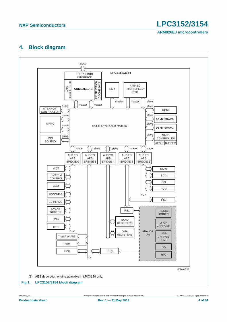
4. Block diagram
(1) AES decryption engine available in LPC3154 only.
Fig 1. LPC3152/3154 block diagram
96 kB ISRAM0
ARM926EJ-S
TEST/DEBUGINTERFACE
DMA
MCISD/SDIO
USB 2.0HIGH-SPEED
OTG
AHB TOAPB
BRIDGE 0
JTAG
WDT
SYSTEMCONTROL
CGU
IOCONFIG
10-bit ADC
RNG
EVENTROUTER
OTP
LPC3152/3154
mastermastermaster
master slave
002aae095
slave
AHB TOAPB
BRIDGE 1
I2C1
PWM
I2C0
TIMER 0/1/2/3
slave
NANDREGISTERS
DMAREGISTERS
AHB TOAPB
BRIDGE 4
slave
slave
96 kB ISRAM1
slave
slave
ROMINTERRUPT
CONTROLLER
slave
slave
slave
slave
slave
MULTI-LAYER AHB MATRIX
DAT
AC
AC
HE
16
kB
INS
TR
UC
TIO
NC
AC
HE
16
kB
UART
LCD
SPI
PCM
AHB TOAPB
BRIDGE 2
MPMC
I2S0
AHB TOAPB
BRIDGE 3
slave slave
I2S1
RTC
PSU
Li-IONCHARGER
ANALOGDIE
AUDIOCODEC
USBCHARGE
PUMP
NANDCONTROLLER
BUFFERAES(1)
LPC3152_54 All information provided in this document is subject to legal disclaimers. © NXP B.V. 2012. All rights reserved.
Product data sheet Rev. 1 — 31 May 2012 4 of 94
NXP Semiconductors LPC3152/3154ARM926EJ microcontrollers
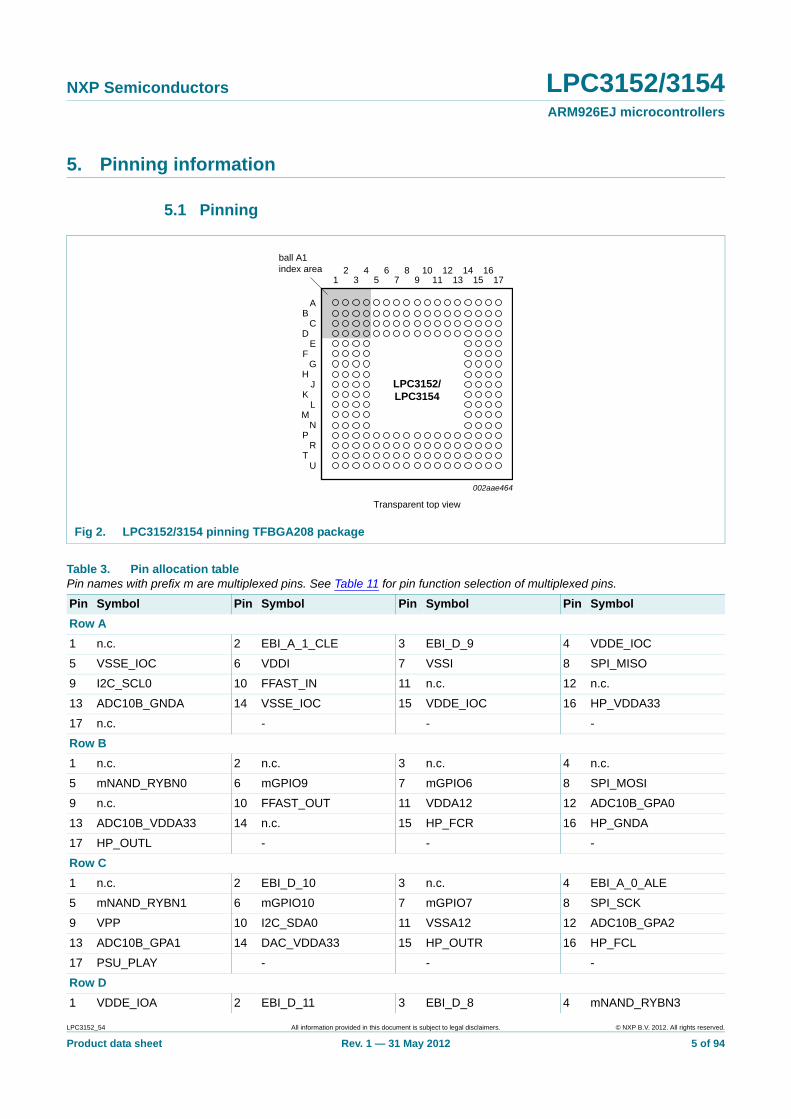
5. Pinning information
5.1 Pinning
Fig 2. LPC3152/3154 pinning TFBGA208 package
002aae464
LPC3152/LPC3154
Transparent top view
ball A1index area
UT
RP
NM
K
H
L
J
GF
ED
C
AB
2 4 6 8 10 1213
1415 17
161 3 5 7 9 11
Table 3. Pin allocation tablePin names with prefix m are multiplexed pins. See Table 11 for pin function selection of multiplexed pins.
Pin Symbol Pin Symbol Pin Symbol Pin Symbol
Row A
1 n.c. 2 EBI_A_1_CLE 3 EBI_D_9 4 VDDE_IOC
5 VSSE_IOC 6 VDDI 7 VSSI 8 SPI_MISO
9 I2C_SCL0 10 FFAST_IN 11 n.c. 12 n.c.
13 ADC10B_GNDA 14 VSSE_IOC 15 VDDE_IOC 16 HP_VDDA33
17 n.c. - - -
Row B
1 n.c. 2 n.c. 3 n.c. 4 n.c.
5 mNAND_RYBN0 6 mGPIO9 7 mGPIO6 8 SPI_MOSI
9 n.c. 10 FFAST_OUT 11 VDDA12 12 ADC10B_GPA0
13 ADC10B_VDDA33 14 n.c. 15 HP_FCR 16 HP_GNDA
17 HP_OUTL - - -
Row C
1 n.c. 2 EBI_D_10 3 n.c. 4 EBI_A_0_ALE
5 mNAND_RYBN1 6 mGPIO10 7 mGPIO7 8 SPI_SCK
9 VPP 10 I2C_SDA0 11 VSSA12 12 ADC10B_GPA2
13 ADC10B_GPA1 14 DAC_VDDA33 15 HP_OUTR 16 HP_FCL
17 PSU_PLAY - - -
Row D
1 VDDE_IOA 2 EBI_D_11 3 EBI_D_8 4 mNAND_RYBN3
LPC3152_54 All information provided in this document is subject to legal disclaimers. © NXP B.V. 2012. All rights reserved.
Product data sheet Rev. 1 — 31 May 2012 5 of 94
NXP Semiconductors LPC3152/3154ARM926EJ microcontrollers
5 mNAND_RYBN2 6 mGPIO8 7 mGPIO5 8 SPI_CS_OUT0
9 SPI_CS_IN 10 PWM_DATA 11 GPIO4 12 GPIO3
13 n.c. 14 HP_OUTC 15 PSU_STOP 16 PSU_VSSA
17 PSU_VSSA_CLEAN - - -
Row E
1 VSSE_IOA 2 EBI_D_12 3 EBI_D_7 4 EBI_D_6
14 HP_VREF 15 RSTIN_N 16 PSU_VBAT 17 PSU_VOUT3
Row F
1 n.c. 2 EBI_D_13 3 EBI_D_5 4 EBI_D_4
14 TDO 15 DAC_VREFN 16 DAC_VREFP 17 PSU_VBAT2
Row G
1 n.c. 2 EBI_D_14 3 n.c. 4 EBI_D_3
14 PSU_VOUT2 15 VDDE_IOD 16 PSU_VIN1 17 PSU_LX2
Row H
1 VSSI 2 EBI_D_15 3 EBI_D_1 4 EBI_D_2
14 PSU_VOUT1 15 PSU_LX1 16 PSU_VSS1 17 PSU_VBAT1
Row J
1 VDDI 2 EBI_NCAS_BLOUT_0 3 EBI_D_0 4 EBI_NRAS_BLOUT_1
14 CHARGE_VBUS 15 CHARGE_VSS 16 PSU_VBUS 17 CHARGE_VNTC
Row K
1 VSSE_IOB 2 n.c. 3 EBI_DQM_0_NOE 4 EBI_NWE
14 RTC_BACKUP 15 CHARGE_CC_REF 16 CHARGE_VBAT 17 CHARGE_BAT_SENSE
Row L
1 VDDE_IOB 2 NAND_NCS_0 3 NAND_NCS_1 4 NAND_NCS_2
14 VSSE_IOD 15 RTC_VDD36 16 FSLOW_OUT 17 FSLOW_IN
Row M
1 VDDE_IOA 2 NAND_NCS_3 3 n.c. 4 CLOCK_OUT
14 VDDI_AD 15 VSSI_AD 16 RTC_INT 17 RTC_VSS
Row N
1 VSSE_IOA 2 USB_VDDA12_PLL 3 USB_VBUS 4 USB_RREF
14 ADC_VDDA33 15 ADC_VDDA18 16 ADC_GNDA 17 UOS_VSS
Row P
1 n.c. 2 USB_VSSA_REF 3 USB_ID 4 mLCD_DB_10
5 mLCD_DB_9 6 mLCD_DB_5 7 mLCD_E_RD 8 mLCD_DB_1
9 I2SRX_DATA0 10 UART_TXD 11 mUART_CTS_N 12 GPIO2
13 ADC_TINL 14 ADC_TINR 15 UOS_VBUS 16 UOS_VBAT
17 UOS_CX2 - - -
Row R
1 USB_DM 2 USB_VSSA_TERM 3 USB_VDDA33 4 mLCD_DB_15
5 mLCD_DB_6 6 mLCD_DB_3 7 mLCD_RS 8 mLCD_CSB
Table 3. Pin allocation table …continuedPin names with prefix m are multiplexed pins. See Table 11 for pin function selection of multiplexed pins.
Pin Symbol Pin Symbol Pin Symbol Pin Symbol
LPC3152_54 All information provided in this document is subject to legal disclaimers. © NXP B.V. 2012. All rights reserved.
Product data sheet Rev. 1 — 31 May 2012 6 of 94
NXP Semiconductors LPC3152/3154ARM926EJ microcontrollers
9 I2SRX_WS0 10 UART_RXD 11 mUART_RTS_N 12 mI2STX_WS0
13 GPIO0 14 ADC_VINR 15 ADC_MIC 16 ADC_VREFN
17 UOS_CX1 - - -
Row T
1 USB_DP 2 USB_GNDA 3 USB_VDDA33_DRV 4 mLCD_DB_12
5 mLCD_DB_7 6 mLCD_DB_2 7 mLCD_DB_0 8 mLCD_RW_WR
9 I2SRX_BCK0 10 TDI 11 mI2STX_CLK0 12 mI2STX_BCK0
13 mI2STX_DATA0 14 GPIO1 15 ADC_VINL 16 ADC_VREF
17 ADC_VREFP - - -
Row U
1 n.c. 2 mLCD_DB_14 3 mLCD_DB_13 4 mLCD_DB_11
5 mLCD_DB_8 6 mLCD_DB_4 7 VDDE_IOB 8 VSSE_IOB
9 TMS 10 JTAGSEL 11 TRST_N 12 TCK
13 VDDI 14 VSSI 15 VDDE_IOC 16 VSSE_IOC
17 RTC_CLK32 - - -
Table 3. Pin allocation table …continuedPin names with prefix m are multiplexed pins. See Table 11 for pin function selection of multiplexed pins.
Pin Symbol Pin Symbol Pin Symbol Pin Symbol
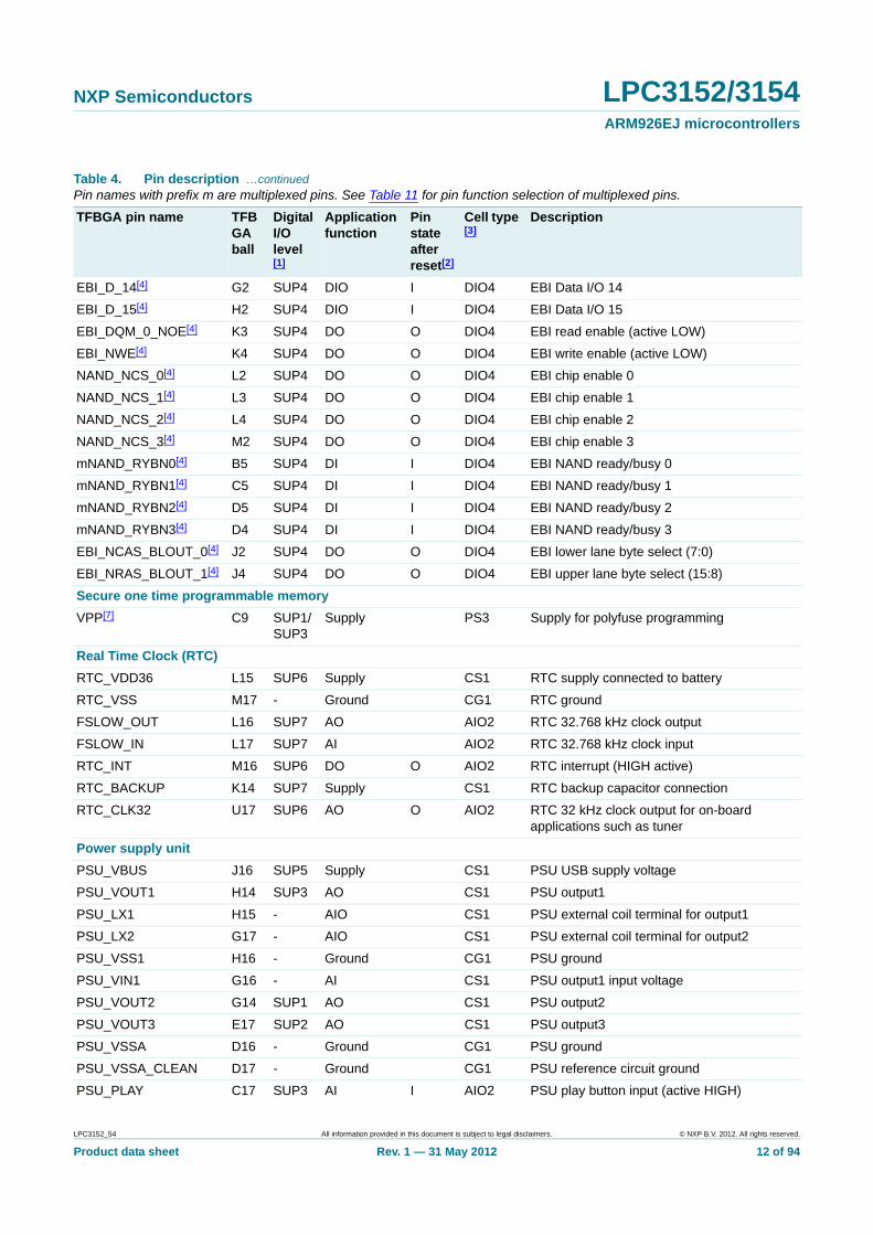
Table 4. Pin description Pin names with prefix m are multiplexed pins. See Table 11 for pin function selection of multiplexed pins.
TFBGA pin name TFBGA ball
Digital I/O level [1]
Application function
Pin state after reset[2]
Cell type [3]
Description
Clock generation unit
FFAST_IN A10 SUP1 AI AIO2 12 MHz oscillator clock input
FFAST_OUT B10 SUP1 AO AIO2 12 MHz oscillator clock output
VDDA12 B11 SUP1 Supply PS3 12 MHz oscillator/PLLs analog supply
VSSA12 C11 - Ground CG1 12 MHz oscillator/PLLs analog ground
RSTIN_N E15 SUP3 DI I:PU DIO2 System reset input (active LOW)
CLOCK_OUT M4 SUP4 DO O DIO4 Clock output
10-bit ADC
ADC10B_VDDA33 B13 SUP3 Supply PS3 10-bit ADC analog supply
ADC10B_GNDA A13 - Ground CG1 10-bit ADC analog ground
ADC10B_GPA0 B12 SUP3 AI AIO1 10-bit ADC analog input
ADC10B_GPA1 C13 SUP3 AI AIO1 10-bit ADC analog input
ADC10B_GPA2 C12 SUP3 AI AIO1 10-bit ADC analog input
Audio ADC
ADC_MIC R15 - AI AIO2 ADC microphone input
ADC_VINL T15 - AI AIO2 ADC line input left
ADC_VINR R14 - AI AIO2 ADC line input right
ADC_TINL P13 - AI AIO2 ADC tuner input left
ADC_TINR P14 - AI AIO2 ADC tuner input right
ADC_VREF T16 - AO AIO2 ADC reference voltage output
LPC3152_54 All information provided in this document is subject to legal disclaimers. © NXP B.V. 2012. All rights reserved.
Product data sheet Rev. 1 — 31 May 2012 7 of 94
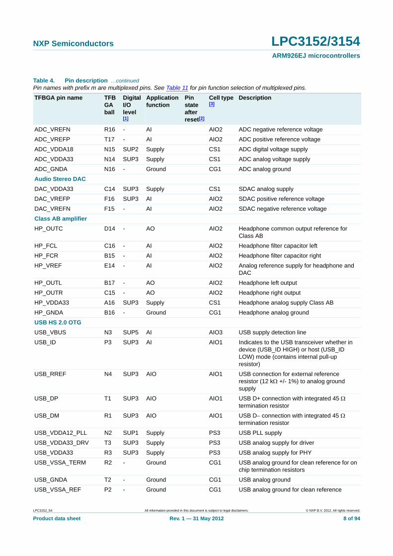
NXP Semiconductors LPC3152/3154ARM926EJ microcontrollers
ADC_VREFN R16 - AI AIO2 ADC negative reference voltage
ADC_VREFP T17 - AI AIO2 ADC positive reference voltage
ADC_VDDA18 N15 SUP2 Supply CS1 ADC digital voltage supply
ADC_VDDA33 N14 SUP3 Supply CS1 ADC analog voltage supply
ADC_GNDA N16 - Ground CG1 ADC analog ground
Audio Stereo DAC
DAC_VDDA33 C14 SUP3 Supply CS1 SDAC analog supply
DAC_VREFP F16 SUP3 AI AIO2 SDAC positive reference voltage
DAC_VREFN F15 - AI AIO2 SDAC negative reference voltage
Class AB amplifier
HP_OUTC D14 - AO AIO2 Headphone common output reference for Class AB
HP_FCL C16 - AI AIO2 Headphone filter capacitor left
HP_FCR B15 - AI AIO2 Headphone filter capacitor right
HP_VREF E14 - AI AIO2 Analog reference supply for headphone and DAC
HP_OUTL B17 - AO AIO2 Headphone left output
HP_OUTR C15 - AO AIO2 Headphone right output
HP_VDDA33 A16 SUP3 Supply CS1 Headphone analog supply Class AB
HP_GNDA B16 - Ground CG1 Headphone analog ground
USB HS 2.0 OTG
USB_VBUS N3 SUP5 AI AIO3 USB supply detection line
USB_ID P3 SUP3 AI AIO1 Indicates to the USB transceiver whether in device (USB_ID HIGH) or host (USB_ID LOW) mode (contains internal pull-up resistor)
USB_RREF N4 SUP3 AIO AIO1 USB connection for external reference resistor (12 k +/- 1%) to analog ground supply
USB_DP T1 SUP3 AIO AIO1 USB D+ connection with integrated 45 termination resistor
USB_DM R1 SUP3 AIO AIO1 USB D connection with integrated 45 termination resistor
USB_VDDA12_PLL N2 SUP1 Supply PS3 USB PLL supply
USB_VDDA33_DRV T3 SUP3 Supply PS3 USB analog supply for driver
USB_VDDA33 R3 SUP3 Supply PS3 USB analog supply for PHY
USB_VSSA_TERM R2 - Ground CG1 USB analog ground for clean reference for on chip termination resistors
USB_GNDA T2 - Ground CG1 USB analog ground
USB_VSSA_REF P2 - Ground CG1 USB analog ground for clean reference
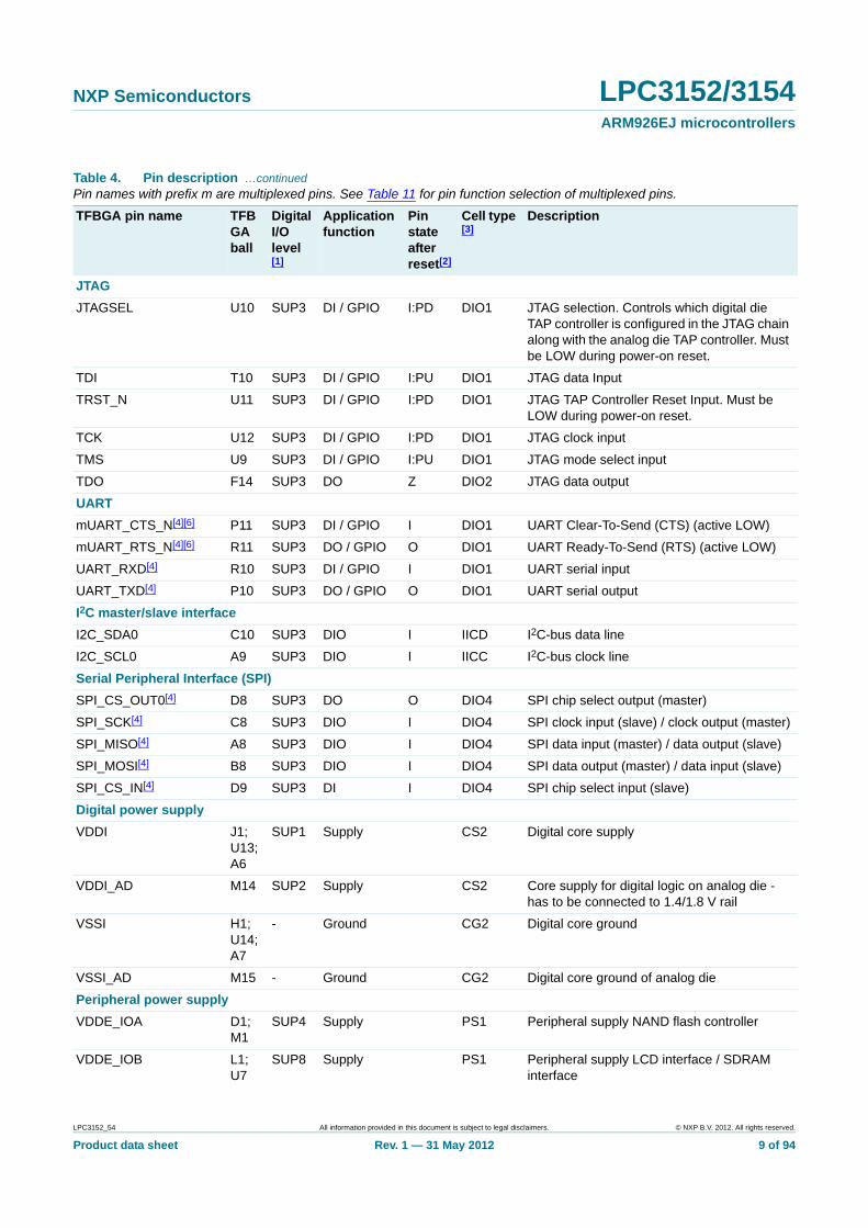
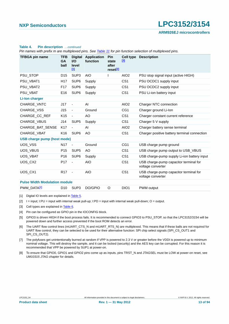
Table 4. Pin description …continuedPin names with prefix m are multiplexed pins. See Table 11 for pin function selection of multiplexed pins.
TFBGA pin name TFBGA ball
Digital I/O level [1]
Application function
Pin state after reset[2]
Cell type [3]
Description
LPC3152_54 All information provided in this document is subject to legal disclaimers. © NXP B.V. 2012. All rights reserved.
Product data sheet Rev. 1 — 31 May 2012 8 of 94
NXP Semiconductors LPC3152/3154ARM926EJ microcontrollers
JTAG
JTAGSEL U10 SUP3 DI / GPIO I:PD DIO1 JTAG selection. Controls which digital die TAP controller is configured in the JTAG chain along with the analog die TAP controller. Must be LOW during power-on reset.
TDI T10 SUP3 DI / GPIO I:PU DIO1 JTAG data Input
TRST_N U11 SUP3 DI / GPIO I:PD DIO1 JTAG TAP Controller Reset Input. Must be LOW during power-on reset.
TCK U12 SUP3 DI / GPIO I:PD DIO1 JTAG clock input
TMS U9 SUP3 DI / GPIO I:PU DIO1 JTAG mode select input
TDO F14 SUP3 DO Z DIO2 JTAG data output
UART
mUART_CTS_N[4][6] P11 SUP3 DI / GPIO I DIO1 UART Clear-To-Send (CTS) (active LOW)
mUART_RTS_N[4][6] R11 SUP3 DO / GPIO O DIO1 UART Ready-To-Send (RTS) (active LOW)
UART_RXD[4] R10 SUP3 DI / GPIO I DIO1 UART serial input
UART_TXD[4] P10 SUP3 DO / GPIO O DIO1 UART serial output
I2C master/slave interface
I2C_SDA0 C10 SUP3 DIO I IICD I2C-bus data line
I2C_SCL0 A9 SUP3 DIO I IICC I2C-bus clock line
Serial Peripheral Interface (SPI)
SPI_CS_OUT0[4] D8 SUP3 DO O DIO4 SPI chip select output (master)
SPI_SCK[4] C8 SUP3 DIO I DIO4 SPI clock input (slave) / clock output (master)
SPI_MISO[4] A8 SUP3 DIO I DIO4 SPI data input (master) / data output (slave)
SPI_MOSI[4] B8 SUP3 DIO I DIO4 SPI data output (master) / data input (slave)
SPI_CS_IN[4] D9 SUP3 DI I DIO4 SPI chip select input (slave)
Digital power supply
VDDI J1; U13; A6
SUP1 Supply CS2 Digital core supply
VDDI_AD M14 SUP2 Supply CS2 Core supply for digital logic on analog die - has to be connected to 1.4/1.8 V rail
VSSI H1; U14; A7
- Ground CG2 Digital core ground
VSSI_AD M15 - Ground CG2 Digital core ground of analog die
Peripheral power supply
VDDE_IOA D1; M1
SUP4 Supply PS1 Peripheral supply NAND flash controller
VDDE_IOB L1; U7
SUP8 Supply PS1 Peripheral supply LCD interface / SDRAM interface
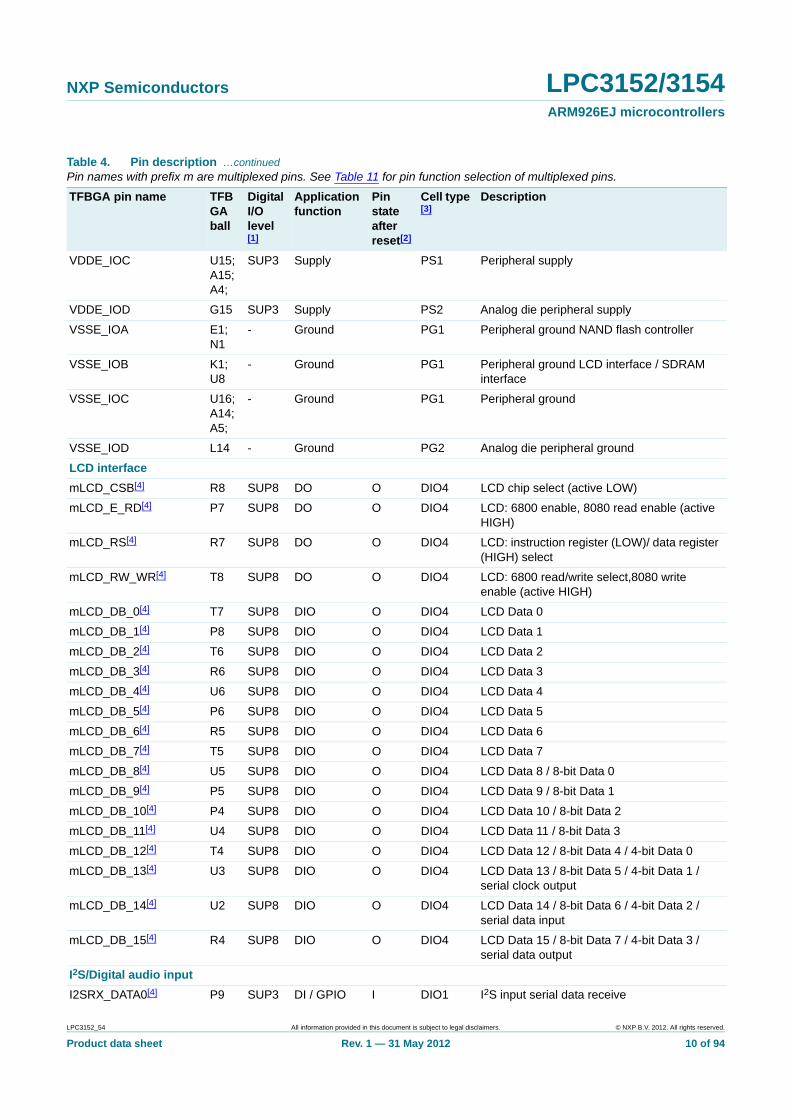
Table 4. Pin description …continuedPin names with prefix m are multiplexed pins. See Table 11 for pin function selection of multiplexed pins.
TFBGA pin name TFBGA ball
Digital I/O level [1]
Application function
Pin state after reset[2]
Cell type [3]
Description
LPC3152_54 All information provided in this document is subject to legal disclaimers. © NXP B.V. 2012. All rights reserved.
Product data sheet Rev. 1 — 31 May 2012 9 of 94
NXP Semiconductors LPC3152/3154ARM926EJ microcontrollers
VDDE_IOC U15; A15; A4;
SUP3 Supply PS1 Peripheral supply
VDDE_IOD G15 SUP3 Supply PS2 Analog die peripheral supply
VSSE_IOA E1; N1
- Ground PG1 Peripheral ground NAND flash controller
VSSE_IOB K1; U8
- Ground PG1 Peripheral ground LCD interface / SDRAM interface
VSSE_IOC U16; A14; A5;
- Ground PG1 Peripheral ground
VSSE_IOD L14 - Ground PG2 Analog die peripheral ground
LCD interface
mLCD_CSB[4] R8 SUP8 DO O DIO4 LCD chip select (active LOW)
mLCD_E_RD[4] P7 SUP8 DO O DIO4 LCD: 6800 enable, 8080 read enable (active HIGH)
mLCD_RS[4] R7 SUP8 DO O DIO4 LCD: instruction register (LOW)/ data register (HIGH) select
mLCD_RW_WR[4] T8 SUP8 DO O DIO4 LCD: 6800 read/write select,8080 write enable (active HIGH)
mLCD_DB_0[4] T7 SUP8 DIO O DIO4 LCD Data 0
mLCD_DB_1[4] P8 SUP8 DIO O DIO4 LCD Data 1
mLCD_DB_2[4] T6 SUP8 DIO O DIO4 LCD Data 2
mLCD_DB_3[4] R6 SUP8 DIO O DIO4 LCD Data 3
mLCD_DB_4[4] U6 SUP8 DIO O DIO4 LCD Data 4
mLCD_DB_5[4] P6 SUP8 DIO O DIO4 LCD Data 5
mLCD_DB_6[4] R5 SUP8 DIO O DIO4 LCD Data 6
mLCD_DB_7[4] T5 SUP8 DIO O DIO4 LCD Data 7
mLCD_DB_8[4] U5 SUP8 DIO O DIO4 LCD Data 8 / 8-bit Data 0
mLCD_DB_9[4] P5 SUP8 DIO O DIO4 LCD Data 9 / 8-bit Data 1
mLCD_DB_10[4] P4 SUP8 DIO O DIO4 LCD Data 10 / 8-bit Data 2
mLCD_DB_11[4] U4 SUP8 DIO O DIO4 LCD Data 11 / 8-bit Data 3
mLCD_DB_12[4] T4 SUP8 DIO O DIO4 LCD Data 12 / 8-bit Data 4 / 4-bit Data 0
mLCD_DB_13[4] U3 SUP8 DIO O DIO4 LCD Data 13 / 8-bit Data 5 / 4-bit Data 1 / serial clock output
mLCD_DB_14[4] U2 SUP8 DIO O DIO4 LCD Data 14 / 8-bit Data 6 / 4-bit Data 2 / serial data input
mLCD_DB_15[4] R4 SUP8 DIO O DIO4 LCD Data 15 / 8-bit Data 7 / 4-bit Data 3 / serial data output
I2S/Digital audio input
I2SRX_DATA0[4] P9 SUP3 DI / GPIO I DIO1 I2S input serial data receive
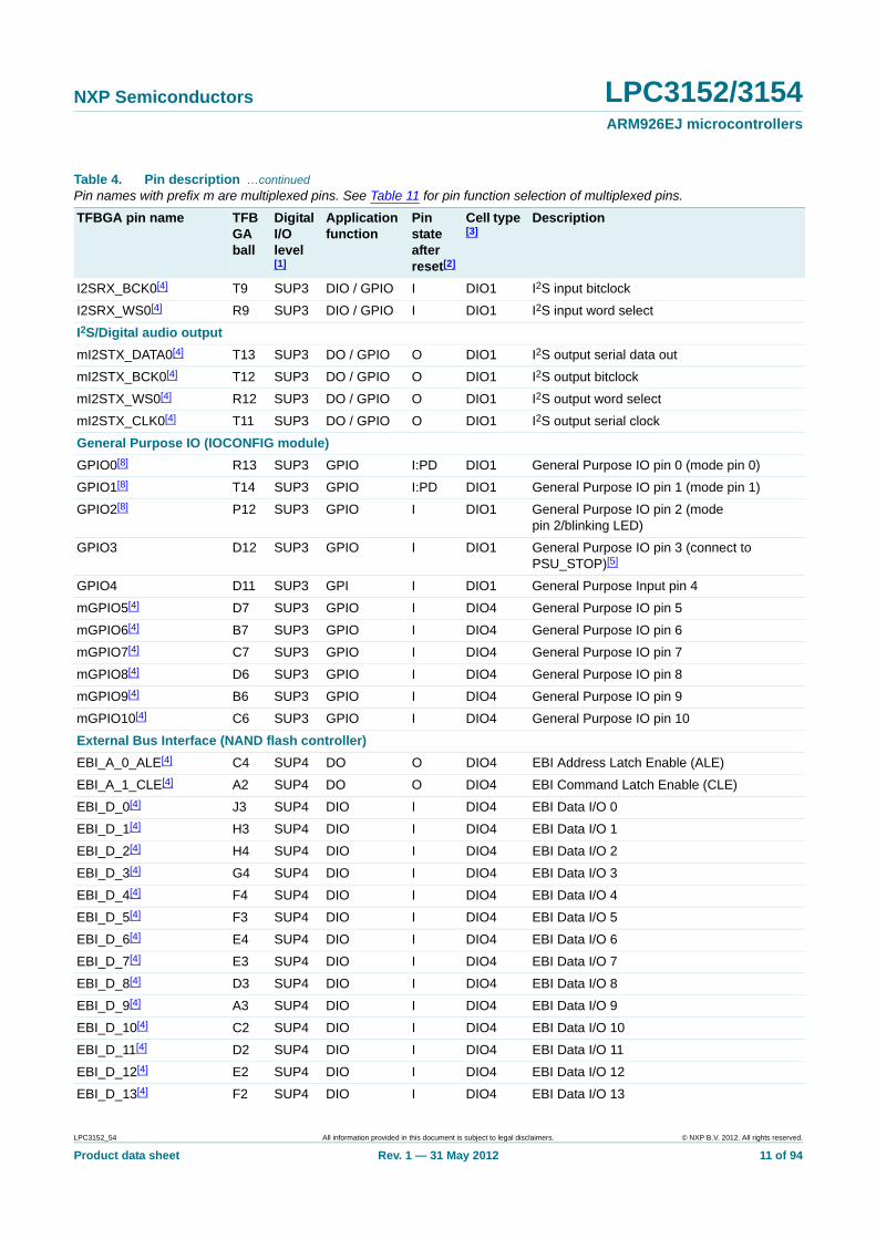
Table 4. Pin description …continuedPin names with prefix m are multiplexed pins. See Table 11 for pin function selection of multiplexed pins.
TFBGA pin name TFBGA ball
Digital I/O level [1]
Application function
Pin state after reset[2]
Cell type [3]
Description
LPC3152_54 All information provided in this document is subject to legal disclaimers. © NXP B.V. 2012. All rights reserved.
Product data sheet Rev. 1 — 31 May 2012 10 of 94
NXP Semiconductors LPC3152/3154ARM926EJ microcontrollers
I2SRX_BCK0[4] T9 SUP3 DIO / GPIO I DIO1 I2S input bitclock
I2SRX_WS0[4] R9 SUP3 DIO / GPIO I DIO1 I2S input word select
I2S/Digital audio output
mI2STX_DATA0[4] T13 SUP3 DO / GPIO O DIO1 I2S output serial data out
mI2STX_BCK0[4] T12 SUP3 DO / GPIO O DIO1 I2S output bitclock
mI2STX_WS0[4] R12 SUP3 DO / GPIO O DIO1 I2S output word select
mI2STX_CLK0[4] T11 SUP3 DO / GPIO O DIO1 I2S output serial clock
General Purpose IO (IOCONFIG module)
GPIO0[8] R13 SUP3 GPIO I:PD DIO1 General Purpose IO pin 0 (mode pin 0)
GPIO1[8] T14 SUP3 GPIO I:PD DIO1 General Purpose IO pin 1 (mode pin 1)
GPIO2[8] P12 SUP3 GPIO I DIO1 General Purpose IO pin 2 (mode pin 2/blinking LED)
GPIO3 D12 SUP3 GPIO I DIO1 General Purpose IO pin 3 (connect to PSU_STOP)[5]
GPIO4 D11 SUP3 GPI I DIO1 General Purpose Input pin 4
mGPIO5[4] D7 SUP3 GPIO I DIO4 General Purpose IO pin 5
mGPIO6[4] B7 SUP3 GPIO I DIO4 General Purpose IO pin 6
mGPIO7[4] C7 SUP3 GPIO I DIO4 General Purpose IO pin 7
mGPIO8[4] D6 SUP3 GPIO I DIO4 General Purpose IO pin 8
mGPIO9[4] B6 SUP3 GPIO I DIO4 General Purpose IO pin 9
mGPIO10[4] C6 SUP3 GPIO I DIO4 General Purpose IO pin 10
External Bus Interface (NAND flash controller)
EBI_A_0_ALE[4] C4 SUP4 DO O DIO4 EBI Address Latch Enable (ALE)
EBI_A_1_CLE[4] A2 SUP4 DO O DIO4 EBI Command Latch Enable (CLE)
EBI_D_0[4] J3 SUP4 DIO I DIO4 EBI Data I/O 0
EBI_D_1[4] H3 SUP4 DIO I DIO4 EBI Data I/O 1
EBI_D_2[4] H4 SUP4 DIO I DIO4 EBI Data I/O 2
EBI_D_3[4] G4 SUP4 DIO I DIO4 EBI Data I/O 3
EBI_D_4[4] F4 SUP4 DIO I DIO4 EBI Data I/O 4
EBI_D_5[4] F3 SUP4 DIO I DIO4 EBI Data I/O 5
EBI_D_6[4] E4 SUP4 DIO I DIO4 EBI Data I/O 6
EBI_D_7[4] E3 SUP4 DIO I DIO4 EBI Data I/O 7
EBI_D_8[4] D3 SUP4 DIO I DIO4 EBI Data I/O 8
EBI_D_9[4] A3 SUP4 DIO I DIO4 EBI Data I/O 9
EBI_D_10[4] C2 SUP4 DIO I DIO4 EBI Data I/O 10
EBI_D_11[4] D2 SUP4 DIO I DIO4 EBI Data I/O 11
EBI_D_12[4] E2 SUP4 DIO I DIO4 EBI Data I/O 12
EBI_D_13[4] F2 SUP4 DIO I DIO4 EBI Data I/O 13
Table 4. Pin description …continuedPin names with prefix m are multiplexed pins. See Table 11 for pin function selection of multiplexed pins.
TFBGA pin name TFBGA ball
Digital I/O level [1]
Application function
Pin state after reset[2]
Cell type [3]
Description
LPC3152_54 All information provided in this document is subject to legal disclaimers. © NXP B.V. 2012. All rights reserved.
Product data sheet Rev. 1 — 31 May 2012 11 of 94
NXP Semiconductors LPC3152/3154ARM926EJ microcontrollers
EBI_D_14[4] G2 SUP4 DIO I DIO4 EBI Data I/O 14
EBI_D_15[4] H2 SUP4 DIO I DIO4 EBI Data I/O 15
EBI_DQM_0_NOE[4] K3 SUP4 DO O DIO4 EBI read enable (active LOW)
EBI_NWE[4] K4 SUP4 DO O DIO4 EBI write enable (active LOW)
NAND_NCS_0[4] L2 SUP4 DO O DIO4 EBI chip enable 0
NAND_NCS_1[4] L3 SUP4 DO O DIO4 EBI chip enable 1
NAND_NCS_2[4] L4 SUP4 DO O DIO4 EBI chip enable 2
NAND_NCS_3[4] M2 SUP4 DO O DIO4 EBI chip enable 3
mNAND_RYBN0[4] B5 SUP4 DI I DIO4 EBI NAND ready/busy 0
mNAND_RYBN1[4] C5 SUP4 DI I DIO4 EBI NAND ready/busy 1
mNAND_RYBN2[4] D5 SUP4 DI I DIO4 EBI NAND ready/busy 2
mNAND_RYBN3[4] D4 SUP4 DI I DIO4 EBI NAND ready/busy 3
EBI_NCAS_BLOUT_0[4] J2 SUP4 DO O DIO4 EBI lower lane byte select (7:0)
EBI_NRAS_BLOUT_1[4] J4 SUP4 DO O DIO4 EBI upper lane byte select (15:8)
Secure one time programmable memory
VPP[7] C9 SUP1/SUP3
Supply PS3 Supply for polyfuse programming
Real Time Clock (RTC)
RTC_VDD36 L15 SUP6 Supply CS1 RTC supply connected to battery
RTC_VSS M17 - Ground CG1 RTC ground
FSLOW_OUT L16 SUP7 AO AIO2 RTC 32.768 kHz clock output
FSLOW_IN L17 SUP7 AI AIO2 RTC 32.768 kHz clock input
RTC_INT M16 SUP6 DO O AIO2 RTC interrupt (HIGH active)
RTC_BACKUP K14 SUP7 Supply CS1 RTC backup capacitor connection
RTC_CLK32 U17 SUP6 AO O AIO2 RTC 32 kHz clock output for on-board applications such as tuner
Power supply unit
PSU_VBUS J16 SUP5 Supply CS1 PSU USB supply voltage
PSU_VOUT1 H14 SUP3 AO CS1 PSU output1
PSU_LX1 H15 - AIO CS1 PSU external coil terminal for output1
PSU_LX2 G17 - AIO CS1 PSU external coil terminal for output2
PSU_VSS1 H16 - Ground CG1 PSU ground
PSU_VIN1 G16 - AI CS1 PSU output1 input voltage
PSU_VOUT2 G14 SUP1 AO CS1 PSU output2
PSU_VOUT3 E17 SUP2 AO CS1 PSU output3
PSU_VSSA D16 - Ground CG1 PSU ground
PSU_VSSA_CLEAN D17 - Ground CG1 PSU reference circuit ground
PSU_PLAY C17 SUP3 AI I AIO2 PSU play button input (active HIGH)
Table 4. Pin description …continuedPin names with prefix m are multiplexed pins. See Table 11 for pin function selection of multiplexed pins.
TFBGA pin name TFBGA ball
Digital I/O level [1]
Application function
Pin state after reset[2]
Cell type [3]
Description
LPC3152_54 All information provided in this document is subject to legal disclaimers. © NXP B.V. 2012. All rights reserved.
Product data sheet Rev. 1 — 31 May 2012 12 of 94
NXP Semiconductors LPC3152/3154ARM926EJ microcontrollers
[1] Digital IO levels are explained in Table 5.
[2] I = input; I:PU = input with internal weak pull-up; I:PD = input with internal weak pull-down; O = output.
[3] Cell types are explained in Table 6.
[4] Pin can be configured as GPIO pin in the IOCONFIG block.
[5] GPIO3 is driven HIGH if the boot process fails. It is recommended to connect GPIO3 to PSU_STOP, so that the LPC3152/3154 will be powered down and further access prevented if the boot ROM detects an error.
[6] The UART flow control lines (mUART_CTS_N and mUART_RTS_N) are multiplexed. This means that if these balls are not required for UART flow control, they can be selected to be used for their alternative function: SPI chip select signals (SPI_CS_OUT1 and SPI_CS_OUT2).
[7] The polyfuses get unintentionally burned at random if VPP is powered to 2.3 V or greater before the VDDI is powered up to minimum nominal voltage. This will destroy the sample, and it can be locked (security) and the AES key can be corrupted. For this reason it is recommended that VPP be powered by SUP1 at power-on.
[8] To ensure that GPIO0, GPIO1 and GPIO2 pins come up as inputs, pins TRST_N and JTAGSEL must be LOW at power-on reset, see UM10315 JTAG chapter for details.
PSU_STOP D15 SUP3 AIO I AIO2 PSU stop signal input (active HIGH)
PSU_VBAT1 H17 SUP6 Supply CS1 PSU DCDC1 supply input
PSU_VBAT2 F17 SUP6 Supply CS1 PSU DCDC2 supply input
PSU_VBAT E16 SUP6 Supply CS1 PSU Li-ion battery input
Li-Ion charger
CHARGE_VNTC J17 - AI AIO2 Charger NTC connection
CHARGE_VSS J15 - Ground CG1 Charger ground Li-Ion
CHARGE_CC_REF K15 - AO CS1 Charger constant current reference
CHARGE_VBUS J14 SUP5 Supply CS1 Charger 5 V supply
CHARGE_BAT_SENSE K17 - AI AIO2 Charger battery sense terminal
CHARGE_VBAT K16 SUP6 AO CS1 Charger positive battery terminal connection
USB charge pump (host mode)
UOS_VSS N17 - Ground CG1 USB charge pump ground
UOS_VBUS P15 SUP5 AO CS1 USB charge pump output to USB_VBUS
UOS_VBAT P16 SUP6 Supply CS1 USB charge-pump supply Li-ion battery input
UOS_CX2 P17 - AIO CS1 USB charge-pump capacitor terminal for voltage converter
UOS_CX1 R17 - AIO CS1 USB charge-pump capacitor terminal for voltage converter
Pulse Width Modulation module
PWM_DATA[4] D10 SUP3 DO/GPIO O DIO1 PWM output
Table 4. Pin description …continuedPin names with prefix m are multiplexed pins. See Table 11 for pin function selection of multiplexed pins.
TFBGA pin name TFBGA ball
Digital I/O level [1]
Application function
Pin state after reset[2]
Cell type [3]
Description
LPC3152_54 All information provided in this document is subject to legal disclaimers. © NXP B.V. 2012. All rights reserved.
Product data sheet Rev. 1 — 31 May 2012 13 of 94
NXP Semiconductors LPC3152/3154ARM926EJ microcontrollers
[1] When the SDRAM is used, the supply voltage of the NAND flash, SDRAM, and the LCD interface must be the same, i.e. SUP4 and SUP8 should be connected to the same rail. (See also Section 6.28.3.).
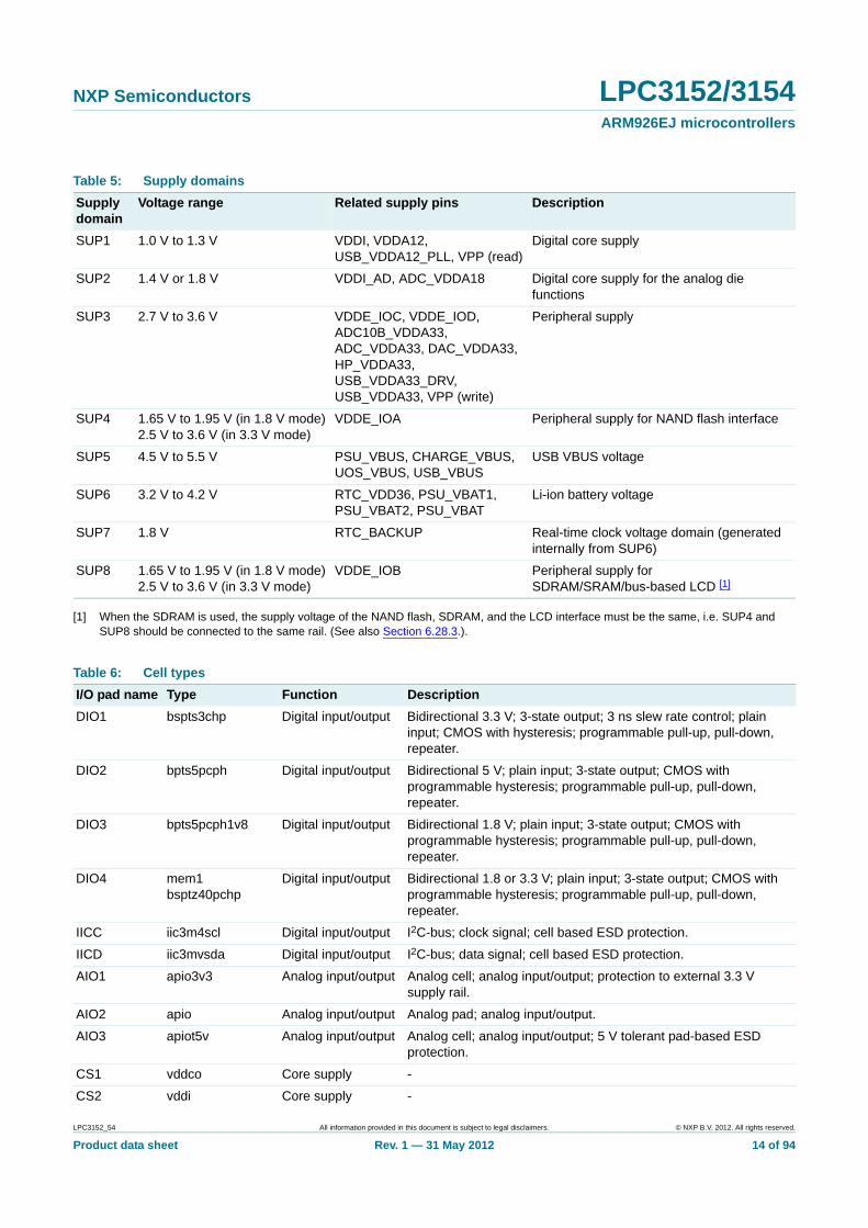
Table 5: Supply domains
Supply domain
Voltage range Related supply pins Description
SUP1 1.0 V to 1.3 V VDDI, VDDA12, USB_VDDA12_PLL, VPP (read)
Digital core supply
SUP2 1.4 V or 1.8 V VDDI_AD, ADC_VDDA18 Digital core supply for the analog die functions
SUP3 2.7 V to 3.6 V VDDE_IOC, VDDE_IOD, ADC10B_VDDA33, ADC_VDDA33, DAC_VDDA33, HP_VDDA33, USB_VDDA33_DRV, USB_VDDA33, VPP (write)
Peripheral supply
SUP4 1.65 V to 1.95 V (in 1.8 V mode)2.5 V to 3.6 V (in 3.3 V mode)
VDDE_IOA Peripheral supply for NAND flash interface
SUP5 4.5 V to 5.5 V PSU_VBUS, CHARGE_VBUS, UOS_VBUS, USB_VBUS
USB VBUS voltage
SUP6 3.2 V to 4.2 V RTC_VDD36, PSU_VBAT1, PSU_VBAT2, PSU_VBAT
Li-ion battery voltage
SUP7 1.8 V RTC_BACKUP Real-time clock voltage domain (generated internally from SUP6)
SUP8 1.65 V to 1.95 V (in 1.8 V mode)2.5 V to 3.6 V (in 3.3 V mode)
VDDE_IOB Peripheral supply for SDRAM/SRAM/bus-based LCD [1]
Table 6: Cell types
I/O pad name Type Function Description
DIO1 bspts3chp Digital input/output Bidirectional 3.3 V; 3-state output; 3 ns slew rate control; plain input; CMOS with hysteresis; programmable pull-up, pull-down, repeater.
DIO2 bpts5pcph Digital input/output Bidirectional 5 V; plain input; 3-state output; CMOS with programmable hysteresis; programmable pull-up, pull-down, repeater.
DIO3 bpts5pcph1v8 Digital input/output Bidirectional 1.8 V; plain input; 3-state output; CMOS with programmable hysteresis; programmable pull-up, pull-down, repeater.
DIO4 mem1bsptz40pchp
Digital input/output Bidirectional 1.8 or 3.3 V; plain input; 3-state output; CMOS with programmable hysteresis; programmable pull-up, pull-down, repeater.
IICC iic3m4scl Digital input/output I2C-bus; clock signal; cell based ESD protection.
IICD iic3mvsda Digital input/output I2C-bus; data signal; cell based ESD protection.
AIO1 apio3v3 Analog input/output Analog cell; analog input/output; protection to external 3.3 V supply rail.
AIO2 apio Analog input/output Analog pad; analog input/output.
AIO3 apiot5v Analog input/output Analog cell; analog input/output; 5 V tolerant pad-based ESD protection.
CS1 vddco Core supply -
CS2 vddi Core supply -
LPC3152_54 All information provided in this document is subject to legal disclaimers. © NXP B.V. 2012. All rights reserved.
Product data sheet Rev. 1 — 31 May 2012 14 of 94
NXP Semiconductors LPC3152/3154ARM926EJ microcontrollers
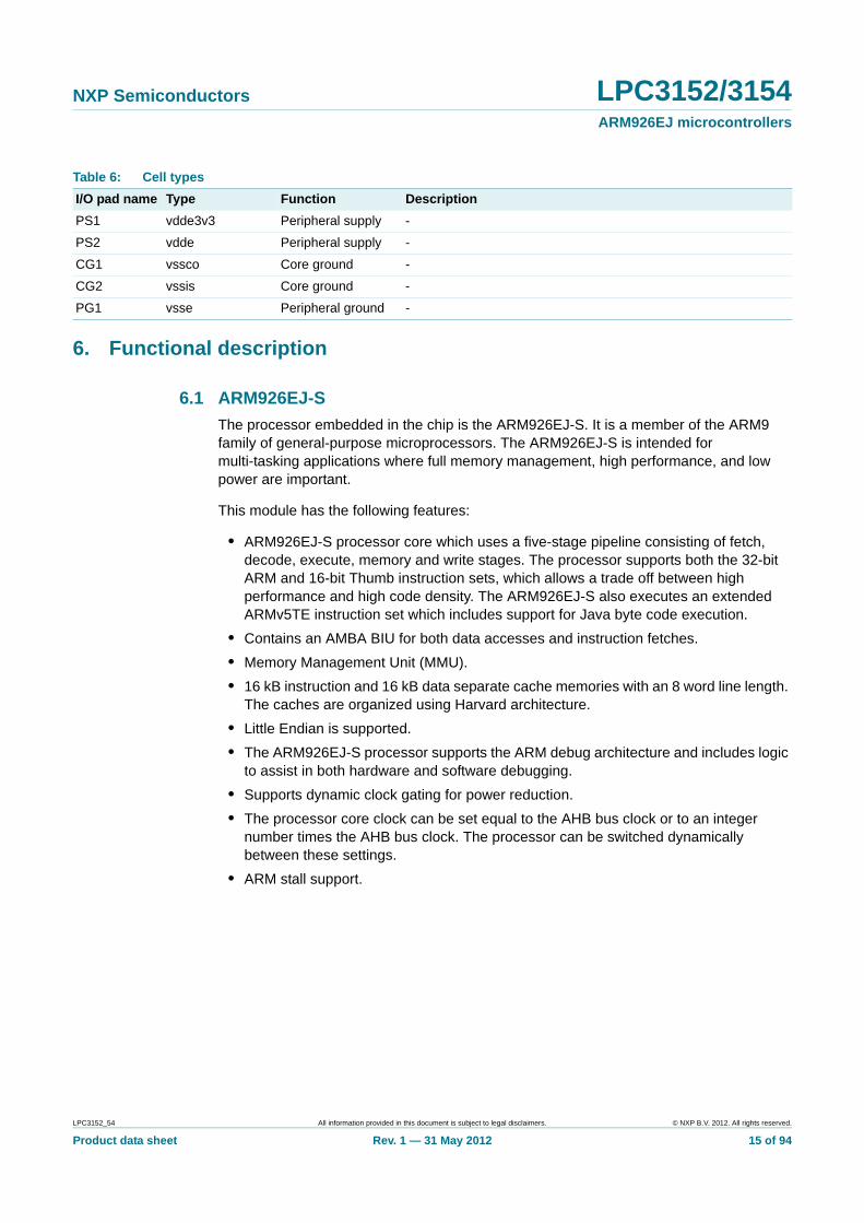
6. Functional description
6.1 ARM926EJ-S
The processor embedded in the chip is the ARM926EJ-S. It is a member of the ARM9 family of general-purpose microprocessors. The ARM926EJ-S is intended for multi-tasking applications where full memory management, high performance, and low power are important.
This module has the following features:
• ARM926EJ-S processor core which uses a five-stage pipeline consisting of fetch, decode, execute, memory and write stages. The processor supports both the 32-bit ARM and 16-bit Thumb instruction sets, which allows a trade off between high performance and high code density. The ARM926EJ-S also executes an extended ARMv5TE instruction set which includes support for Java byte code execution.
• Contains an AMBA BIU for both data accesses and instruction fetches.
• Memory Management Unit (MMU).
• 16 kB instruction and 16 kB data separate cache memories with an 8 word line length. The caches are organized using Harvard architecture.
• Little Endian is supported.
• The ARM926EJ-S processor supports the ARM debug architecture and includes logic to assist in both hardware and software debugging.
• Supports dynamic clock gating for power reduction.
• The processor core clock can be set equal to the AHB bus clock or to an integer number times the AHB bus clock. The processor can be switched dynamically between these settings.
• ARM stall support.
PS1 vdde3v3 Peripheral supply -
PS2 vdde Peripheral supply -
CG1 vssco Core ground -
CG2 vssis Core ground -
PG1 vsse Peripheral ground -
Table 6: Cell types
I/O pad name Type Function Description
LPC3152_54 All information provided in this document is subject to legal disclaimers. © NXP B.V. 2012. All rights reserved.
Product data sheet Rev. 1 — 31 May 2012 15 of 94
NXP Semiconductors LPC3152/3154ARM926EJ microcontrollers
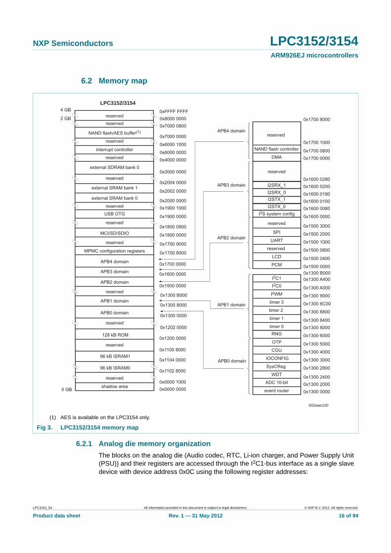
6.2 Memory map
6.2.1 Analog die memory organization
The blocks on the analog die (Audio codec, RTC, Li-ion charger, and Power Supply Unit (PSU)) and their registers are accessed through the I2C1-bus interface as a single slave device with device address 0x0C using the following register addresses:
(1) AES is available on the LPC3154 only.
Fig 3. LPC3152/3154 memory map
0x0000 00000x0000 1000
0 GB
2 GB
4 GB
0x1102 8000
0x1104 0000
0x1105 8000
0x1200 0000
0x1202 0000
0x1300 0000
0x1300 8000
0x1300 B000
0x1500 0000
0x1600 0000
reserved
96 kB ISRAM0
96 kB ISRAM1
128 kB ROM
reserved
reserved
reserved
reserved
reserved
external SRAM bank 0
external SRAM bank 1
external SDRAM bank 0
reserved
reserved
APB0 domain
APB1 domain
APB2 domain
APB3 domain0x1700 0000
0x1700 8000
0x1700 9000
0x1800 0000
0x1800 0900
0x1900 0000
0x1900 10000x2000 0000
0x2002 0000
0x2004 0000
0x3000 0000
0x4000 00000x6000 0000
0x6000 1000
0x7000 0000
0x7000 08000x8000 00000xFFFF FFFF
reserved
MCI/SD/SDIO
USB OTG
APB4 domain
MPMC configuration registers
shadow area
LPC3152/3154
interrupt controller
NAND flash/AES buffer(1)
reservedreserved
0x1300 20000x1300 2400
0x1300 0000event router
ADC 10-bit
0x1300 2800
0x1300 3000
0x1300 4000
0x1300 6000
0x1300 5000
SysCReg
IOCONFIG
CGU
OTP
RNG
APB0 domain
0x1500 0400
0x1500 0000PCM
reserved
LCD0x1500 0800
0x1500 1000
0x1500 2000
0x1600 0000
0x1500 3000
reserved
UART
SPIAPB2 domain
0x1700 08000x1700 0000DMA
NAND flash controller0x1700 1000
0x1700 8000
reserved APB4 domain
reserved
0x1600 0080
APB3 domain
0x1300 84000x1300 8000timer 0
timer 10x1300 8800
0x1300 8C00
0x1300 9000
0x1300 A4000x1300 B000
0x1300 A000
timer 2
timer 3
PWM
I2C0I2C1
APB1 domain
reserved
002aae100
I2S system config
0x1600 0100I2STX_0
0x1600 0180I2STX_1
0x1600 0200I2SRX_0
0x1600 0280I2SRX_1
WDT
LPC3152_54 All information provided in this document is subject to legal disclaimers. © NXP B.V. 2012. All rights reserved.
Product data sheet Rev. 1 — 31 May 2012 16 of 94
NXP Semiconductors LPC3152/3154ARM926EJ microcontrollers
6.3 JTAG
The JTAG interface allows the incorporation of the LPC3152/3154 in a JTAG scan chain.
This module has the following features:
• ARM926 debug access
• Boundary scan
• The ARM926 debug access can be permanently disabled through the JTAG security bits in the One-Time Programmable memory (OTP) block.
6.4 NAND flash controller
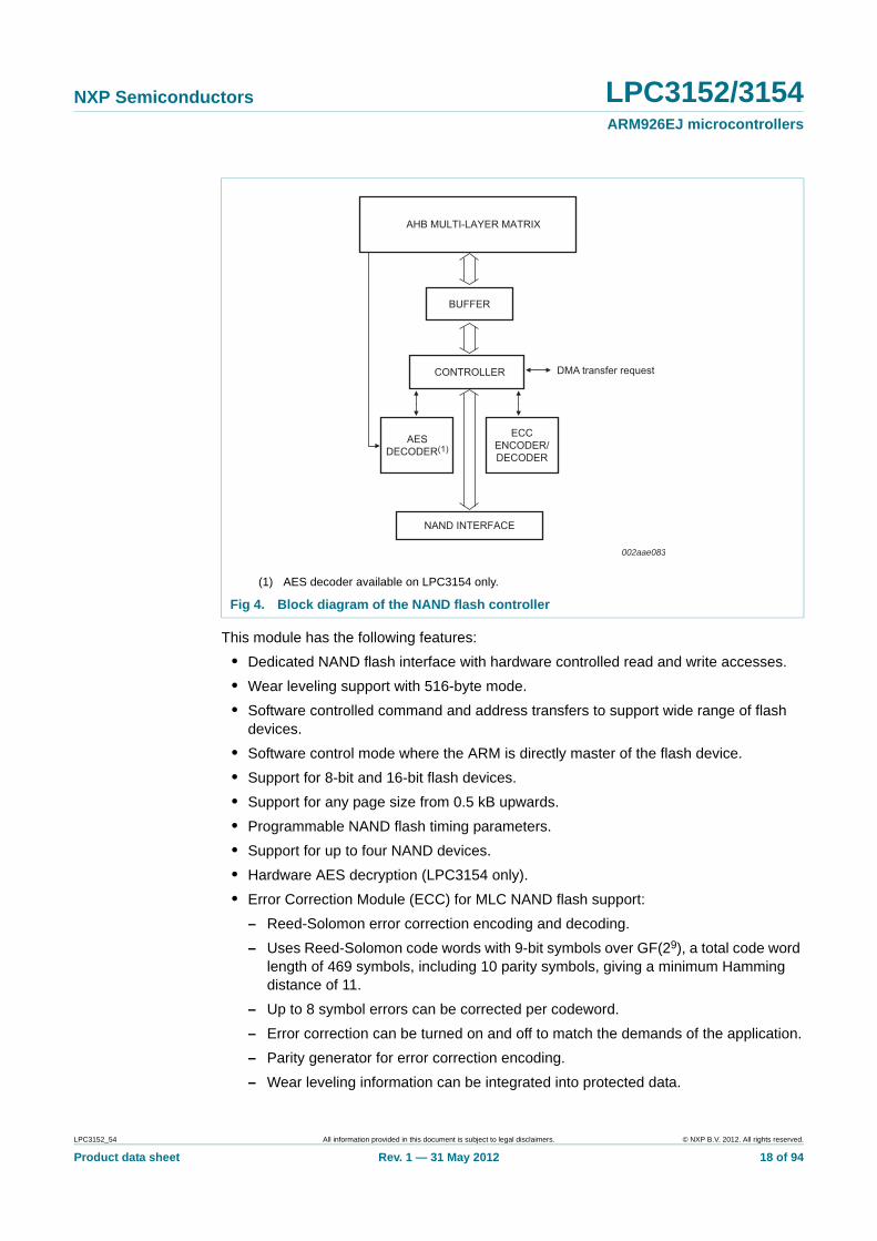
The NAND flash controller is used as a dedicated interface to NAND flash devices. Figure 4 shows a block diagram of the NAND flash controller module. The heart of the module is formed by a controller block that controls the flow of data from/to the AHB bus through the NAND flash controller block to/from the (external) NAND flash. An error correction encoder/decoder module allows for hardware error correction for support of Multi-Level Cell (MLC) NAND flash devices. In the LPC3154, the NAND flash controller is connected to the AES block to support secure (encrypted) code execution (see Section 6.21).
Before data is written from the buffer to the NAND flash, optionally it is first protected by an error correction code generated by the ECC module. After data is read from the NAND flash, the error correction module corrects errors, and/or the AES decryption module can decrypt data.
Table 7. Analog die register addresses (I2C1 slave device address 0x0C)
Block Address offset
PSU/Li-ion charger 0x0000 - 0x000F
Audio codec 0x0010 - 0x001F
RTC 0x0020 - 0x002F
LPC3152_54 All information provided in this document is subject to legal disclaimers. © NXP B.V. 2012. All rights reserved.
Product data sheet Rev. 1 — 31 May 2012 17 of 94
NXP Semiconductors LPC3152/3154ARM926EJ microcontrollers
This module has the following features:
• Dedicated NAND flash interface with hardware controlled read and write accesses.
• Wear leveling support with 516-byte mode.
• Software controlled command and address transfers to support wide range of flash devices.
• Software control mode where the ARM is directly master of the flash device.
• Support for 8-bit and 16-bit flash devices.
• Support for any page size from 0.5 kB upwards.
• Programmable NAND flash timing parameters.
• Support for up to four NAND devices.
• Hardware AES decryption (LPC3154 only).
• Error Correction Module (ECC) for MLC NAND flash support:
– Reed-Solomon error correction encoding and decoding.
– Uses Reed-Solomon code words with 9-bit symbols over GF(29), a total code word length of 469 symbols, including 10 parity symbols, giving a minimum Hamming distance of 11.
– Up to 8 symbol errors can be corrected per codeword.
– Error correction can be turned on and off to match the demands of the application.
– Parity generator for error correction encoding.
– Wear leveling information can be integrated into protected data.
(1) AES decoder available on LPC3154 only.
Fig 4. Block diagram of the NAND flash controller
002aae083
AHB MULTI-LAYER MATRIX
BUFFER
CONTROLLER
AESDECODER(1)
ECCENCODER/DECODER
NAND INTERFACE
DMA transfer request
LPC3152_54 All information provided in this document is subject to legal disclaimers. © NXP B.V. 2012. All rights reserved.
Product data sheet Rev. 1 — 31 May 2012 18 of 94
NXP Semiconductors LPC3152/3154ARM926EJ microcontrollers
– Interrupts generated after completion of error correction task with three interrupt registers.
– Error correction statistics distributed to ARM using interrupt scheme.
– Interface is compatible with the ARM External Bus Interface (EBI).
6.5 Multi-Port Memory Controller (MPMC)
The multi-port memory controller supports the interface to different memory types, for example:
• SDRAM
• Low-power SDRAM
• Static memory interface
This module has the following features:
• Dynamic memory interface support including SDRAM, JEDEC low-power SDRAM.
• Address line supporting up to 128 MB (two 64Mx8 devices connected to a single chip select) of dynamic memory.
• The MPMC has two AHB interfaces:
a. an interface for accessing external memory.
b. a separate control interface to program the MPMC. This enables the MPMC registers to be situated in memory with other system peripheral registers.
• Low transaction latency.
• Read and write buffers to reduce latency and to improve performance, particularly for un-cached processors.
• Static memory features include:
– asynchronous page mode read
– programmable wait states
– bus turnaround delay
– output enable, and write enable delays
– extended wait
• One chip select for synchronous memory and two chip selects for static memory devices.
• Power-saving modes.
• Dynamic memory self-refresh mode supported.
• Controller support for 2 k, 4 k, and 8 k row address synchronous memory parts.
• Support for all AHB burst types.
• Little and big-endian support.
• Support for the External Bus Interface (EBI) that enables the memory controller pads to be shared.
LPC3152_54 All information provided in this document is subject to legal disclaimers. © NXP B.V. 2012. All rights reserved.
Product data sheet Rev. 1 — 31 May 2012 19 of 94
NXP Semiconductors LPC3152/3154ARM926EJ microcontrollers
6.6 External Bus Interface (EBI)
The EBI module acts as multiplexer with arbitration between the NAND flash and the SDRAM/SRAM memory modules connected externally through the MPMC.
The main purpose for using the EBI module is to save external pins. However only data and address pins are multiplexed. Control signals towards and from the external memory devices are not multiplexed.
6.7 Internal ROM Memory
The internal ROM memory is used to store the boot code of the LPC3152/3154. After a reset, the ARM processor will start its code execution from this memory.
The LPC3154 ROM memory has the following features:
• Supports secure booting from SPI flash, NAND flash, SD/SDHC/MMC cards, UART, and USB (DFU class) interfaces.
• Supports SHA1 hash checking on the boot image.
• Supports un-secure boot from UART and USB (DFU class) interfaces during development. Once the AES key is programmed in the OTP, only secure boot is allowed through UART and USB.
• Supports secure booting from managed NAND devices such as moviNAND, iNAND, eMMC-NAND and eSD-NAND using SD/MMC boot mode.
• Contains pre-defined MMU table (16 kB) for simple systems.
The LPC3152 ROM memory has the following features:
• Supports non-secure booting from SPI flash, NAND flash, SD/SDHC/MMC cards, UART, and USB (DFU class) interfaces.
• Supports option to perform CRC32 checking on the boot image.
• Supports non-secure booting from UART and USB (DFU class) interfaces during development.
• Supports non-secure booting from managed NAND devices such as moviNAND, iNAND, eMMC-NAND and eSD-NAND using SD/MMC boot mode.
• Contains pre-defined MMU table (16 kB) for simple systems.
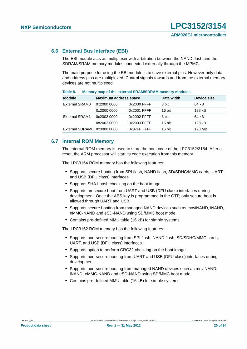
Table 8. Memory map of the external SRAM/SDRAM memory modules
Module Maximum address space Data width Device size
External SRAM0 0x2000 0000 0x2000 FFFF 8 bit 64 kB
0x2000 0000 0x2001 FFFF 16 bit 128 kB
External SRAM1 0x2002 0000 0x2002 FFFF 8 bit 64 kB
0x2002 0000 0x2003 FFFF 16 bit 128 kB
External SDRAM0 0x3000 0000 0x37FF FFFF 16 bit 128 MB
LPC3152_54 All information provided in this document is subject to legal disclaimers. © NXP B.V. 2012. All rights reserved.
Product data sheet Rev. 1 — 31 May 2012 20 of 94
NXP Semiconductors LPC3152/3154ARM926EJ microcontrollers
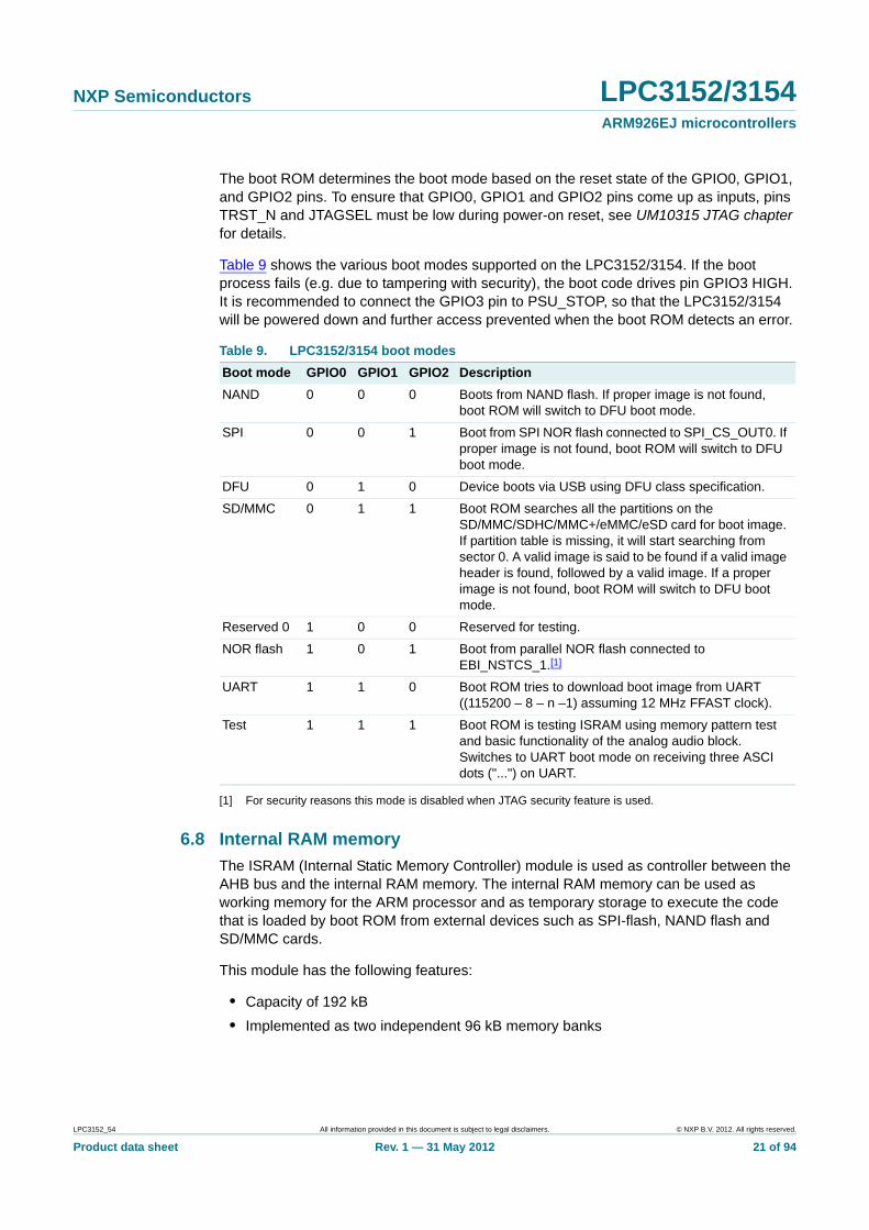
The boot ROM determines the boot mode based on the reset state of the GPIO0, GPIO1, and GPIO2 pins. To ensure that GPIO0, GPIO1 and GPIO2 pins come up as inputs, pins TRST_N and JTAGSEL must be low during power-on reset, see UM10315 JTAG chapter for details.
Table 9 shows the various boot modes supported on the LPC3152/3154. If the boot process fails (e.g. due to tampering with security), the boot code drives pin GPIO3 HIGH. It is recommended to connect the GPIO3 pin to PSU_STOP, so that the LPC3152/3154 will be powered down and further access prevented when the boot ROM detects an error.
[1] For security reasons this mode is disabled when JTAG security feature is used.
6.8 Internal RAM memory
The ISRAM (Internal Static Memory Controller) module is used as controller between the AHB bus and the internal RAM memory. The internal RAM memory can be used as working memory for the ARM processor and as temporary storage to execute the code that is loaded by boot ROM from external devices such as SPI-flash, NAND flash and SD/MMC cards.
This module has the following features:
• Capacity of 192 kB
• Implemented as two independent 96 kB memory banks
Table 9. LPC3152/3154 boot modes
Boot mode GPIO0 GPIO1 GPIO2 Description
NAND 0 0 0 Boots from NAND flash. If proper image is not found, boot ROM will switch to DFU boot mode.
SPI 0 0 1 Boot from SPI NOR flash connected to SPI_CS_OUT0. If proper image is not found, boot ROM will switch to DFU boot mode.
DFU 0 1 0 Device boots via USB using DFU class specification.
SD/MMC 0 1 1 Boot ROM searches all the partitions on the SD/MMC/SDHC/MMC+/eMMC/eSD card for boot image. If partition table is missing, it will start searching from sector 0. A valid image is said to be found if a valid image header is found, followed by a valid image. If a proper image is not found, boot ROM will switch to DFU boot mode.
Reserved 0 1 0 0 Reserved for testing.
NOR flash 1 0 1 Boot from parallel NOR flash connected to EBI_NSTCS_1.[1]
UART 1 1 0 Boot ROM tries to download boot image from UART ((115200 – 8 – n –1) assuming 12 MHz FFAST clock).
Test 1 1 1 Boot ROM is testing ISRAM using memory pattern test and basic functionality of the analog audio block. Switches to UART boot mode on receiving three ASCI dots ("...") on UART.
LPC3152_54 All information provided in this document is subject to legal disclaimers. © NXP B.V. 2012. All rights reserved.
Product data sheet Rev. 1 — 31 May 2012 21 of 94
NXP Semiconductors LPC3152/3154ARM926EJ microcontrollers
6.9 Memory Card Interface (MCI)
The MCI controller interface can be used to access memory cards according to the Secure Digital (SD) and Multi-Media Card (MMC) standards. The host controller can be used to interface to small form factor expansion cards compliant to the SDIO card standard as well. Finally, the MCI supports CE-ATA 1.1 compliant hard disk drives.
This module has the following features:
• One 8-bit wide interface.
• Supports high-speed SD, versions 1.01, 1.10 and 2.0.
• Supports SDIO version 1.10.
• Supports MMCplus, MMCmobile, and MMCmicro cards based on MMC 4.1.
• Supports SDHC memory cards.
• CRC generation and checking.
• Supports 1/4-bit SD cards.
• Card detection and write protection.
• FIFO buffers of 16 bytes deep.
• Host pull-up control.
• SDIO suspend and resume.
• 1-byte to 65 535-byte blocks.
• Suspend and resume operations.
• SDIO Read-wait.
• Maximum clock speed of 52 MHz (MMC 4.1).
• Supports CE-ATA 1.1.
• Supports 1-bit, 4-bit, and 8-bit MMC cards and CE-ATA devices.
6.10 Universal Serial Bus 2.0 High Speed On-The-Go (OTG)
The USB OTG module allows the LPC3152/3154 to connect directly to a USB host such as a PC (in device mode) or to a USB device in host mode. In addition, the LPC3152/3154 has a special, built-in mode in which it enumerates as a Device Firmware Upgrade (DFU) class, which allows for a (factory) download of the device firmware through USB.
This module has the following features:
• Complies with Universal Serial Bus specification 2.0.
• Complies with USB On-The-Go supplement.
• Complies with Enhanced Host Controller Interface Specification.
• Supports auto USB 2.0 mode discovery.
• Supports all high-speed USB-compliant peripherals.
• Supports all full-speed USB-compliant peripherals.
• Supports software Host Negotiation Protocol (HNP) and Session Request Protocol (SRP) for OTG peripherals.
• Contains UTMI+ compliant transceiver (PHY).
• Supports Interrupts.
LPC3152_54 All information provided in this document is subject to legal disclaimers. © NXP B.V. 2012. All rights reserved.Product data sheet Rev. 1 — 31 May 2012 22 of 94
NXP Semiconductors LPC3152/3154ARM926EJ microcontrollers
• This module has its own, integrated DMA engine.
USB-IF TestID for Hi-speed peripheral silicon and embedded host silicon: 40720018
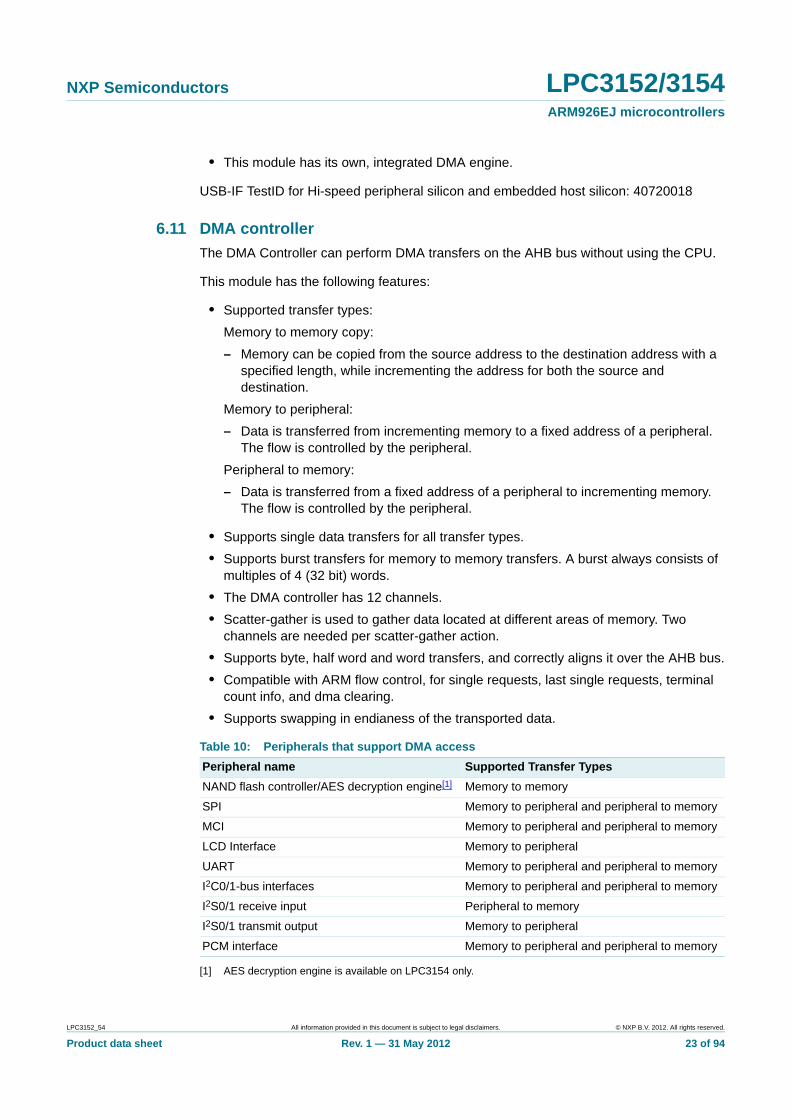
6.11 DMA controller
The DMA Controller can perform DMA transfers on the AHB bus without using the CPU.
This module has the following features:
• Supported transfer types:
Memory to memory copy:
– Memory can be copied from the source address to the destination address with a specified length, while incrementing the address for both the source and destination.
Memory to peripheral:
– Data is transferred from incrementing memory to a fixed address of a peripheral. The flow is controlled by the peripheral.
Peripheral to memory:
– Data is transferred from a fixed address of a peripheral to incrementing memory. The flow is controlled by the peripheral.
• Supports single data transfers for all transfer types.
• Supports burst transfers for memory to memory transfers. A burst always consists of multiples of 4 (32 bit) words.
• The DMA controller has 12 channels.
• Scatter-gather is used to gather data located at different areas of memory. Two channels are needed per scatter-gather action.
• Supports byte, half word and word transfers, and correctly aligns it over the AHB bus.
• Compatible with ARM flow control, for single requests, last single requests, terminal count info, and dma clearing.
• Supports swapping in endianess of the transported data.
[1] AES decryption engine is available on LPC3154 only.
Table 10: Peripherals that support DMA access
Peripheral name Supported Transfer Types
NAND flash controller/AES decryption engine[1] Memory to memory
SPI Memory to peripheral and peripheral to memory
MCI Memory to peripheral and peripheral to memory
LCD Interface Memory to peripheral
UART Memory to peripheral and peripheral to memory
I2C0/1-bus interfaces Memory to peripheral and peripheral to memory
I2S0/1 receive input Peripheral to memory
I2S0/1 transmit output Memory to peripheral
PCM interface Memory to peripheral and peripheral to memory
LPC3152_54 All information provided in this document is subject to legal disclaimers. © NXP B.V. 2012. All rights reserved.
Product data sheet Rev. 1 — 31 May 2012 23 of 94
NXP Semiconductors LPC3152/3154ARM926EJ microcontrollers
6.12 Interrupt controller
The interrupt controller collects interrupt requests from multiple devices, masks interrupt requests, and forwards the combined requests to the processor. The interrupt controller also provides facilities to identify the interrupt requesting devices to be served.
This module has the following features:
• The interrupt controller decodes all the interrupt requests issued by the on-chip peripherals.
• Two interrupt lines (Fast Interrupt Request (FIQ) and Interrupt Request (IRQ)) to the ARM core. The ARM core supports two distinct levels of priority on all interrupt sources, FIQ for high priority interrupts and IRQ for normal priority interrupts.
• Software interrupt request capability associated with each request input.
• Visibility of interrupts request state before masking.
• Support for nesting of interrupt service routines.
• Interrupts routed to IRQ and to FIQ are vectored.
• Level interrupt support.
The following blocks can generate interrupts:
• NAND flash controller
• USB 2.0 HS OTG
• Event router
• 10 bit ADC
• UART
• LCD int
• MCI
• SPI
• I2C0-bus and I2C1-bus
• Timer 0, timer 1, timer 2, and timer 3
• I2S transmit: I2STX_0 and I2STX_1
• I2S receive: I2SRX_0 and I2SRX_1
• DMA
6.13 Multi-layer AHB
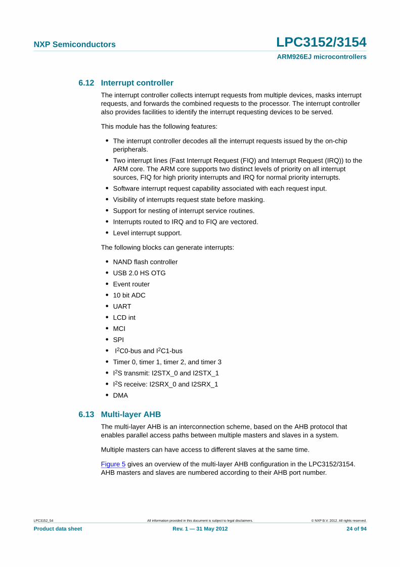
The multi-layer AHB is an interconnection scheme, based on the AHB protocol that enables parallel access paths between multiple masters and slaves in a system.
Multiple masters can have access to different slaves at the same time.
Figure 5 gives an overview of the multi-layer AHB configuration in the LPC3152/3154. AHB masters and slaves are numbered according to their AHB port number.
LPC3152_54 All information provided in this document is subject to legal disclaimers. © NXP B.V. 2012. All rights reserved.
Product data sheet Rev. 1 — 31 May 2012 24 of 94
NXP Semiconductors LPC3152/3154ARM926EJ microcontrollers
(1) AES decryption engine is available on LPC3154 only.
Fig 5. LPC3152/3154 AHB multi-layer matrix connections
master
= master/slave connection supported by matrix
002aae080
USB-OTGAHB
MASTER
30
DMA
2
I-CA
CH
E
D-C
AC
HE
1
ARM926EJ-S
AHB-APBBRIDGE 0
AHB-APBBRIDGE 1
AHB-APBBRIDGE 3
AHB-APBBRIDGE 4
NAND CONTROLLER
INTERRUPT CONTROLLER
PWM I2C1I2C0TIMER 0
10-bit ADC
CGU
WDT SYSTEM CONTROL
IOCONFIG
EVENT ROUTER
RNG OTP
I2S0/1
NAND REGISTERSDMA REGISTERS
TIMER 1 TIMER 2 TIMER 3
AHB-APBBRIDGE 2
UARTLCD SPIPCM
slave
MULTI-LAYER AHB MATRIX
0
1
2
3
4
5
MCI SD/SDIO7
USB HIGH-SPEED OTG8
ISRAM 09
ISRAM 110
ISROM 11
MPMC CONFIG
MPMC CONTROLLER 13
12
6
0
0
1 2 3
0 1 2 3
5 467
0 1 2 3 4 5 6
0 1
AES(1)
BUFFER
LPC3152_54 All information provided in this document is subject to legal disclaimers. © NXP B.V. 2012. All rights reserved.
Product data sheet Rev. 1 — 31 May 2012 25 of 94
NXP Semiconductors LPC3152/3154ARM926EJ microcontrollers
This module has the following features:
• Supports all combinations of 32-bit masters and slaves (fully connected interconnect matrix).
• Round-Robin priority mechanism for bus arbitration: all masters have the same priority and get bus access in their natural order
• Four devices on a master port (listed in their natural order for bus arbitration):
– DMA
– ARM926 instruction port
– ARM926 data port
– USB OTG
• Devices on a slave port (some ports are shared between multiple devices):
– AHB to APB Bridge 0
– AHB to APB Bridge 1
– AHB to APB Bridge 2
– AHB to APB Bridge 3
– AHB to APB Bridge 4
– Interrupt controller
– NAND flash controller
– MCI SD/SDIO
– USB 2.0 HS OTG
– 96 kB ISRAM0
– 96 kB ISRAM1
– 128 kB ROM
– MPMC (Multi-Purpose Memory Controller)
6.14 APB bridge
The APB Bridge is a bus bridge between AMBA Advanced High-performance Bus (AHB) and the ARM Peripheral Bus (APB) interface.
The module supports two different architectures:
• Single Clock Architecture, synchronous bridge. The same clock is used at the AHB side and at the APB side of the bridge. The AHB-to-APB4 bridge uses this architecture.
• Dual Clock Architecture, asynchronous bridge. Different clocks are used at the AHB side and at the APB side of the bridge. The AHB-to-APB0, AHB-to-APB1, AHB-to-APB2, and AHB-to-APB3 bridges use this architecture.
6.15 Clock Generation Unit (CGU)
The clock generation unit generates all clock signals in the system and controls the reset signals for all modules.
LPC3152_54 All information provided in this document is subject to legal disclaimers. © NXP B.V. 2012. All rights reserved.
Product data sheet Rev. 1 — 31 May 2012 26 of 94
NXP Semiconductors LPC3152/3154ARM926EJ microcontrollers
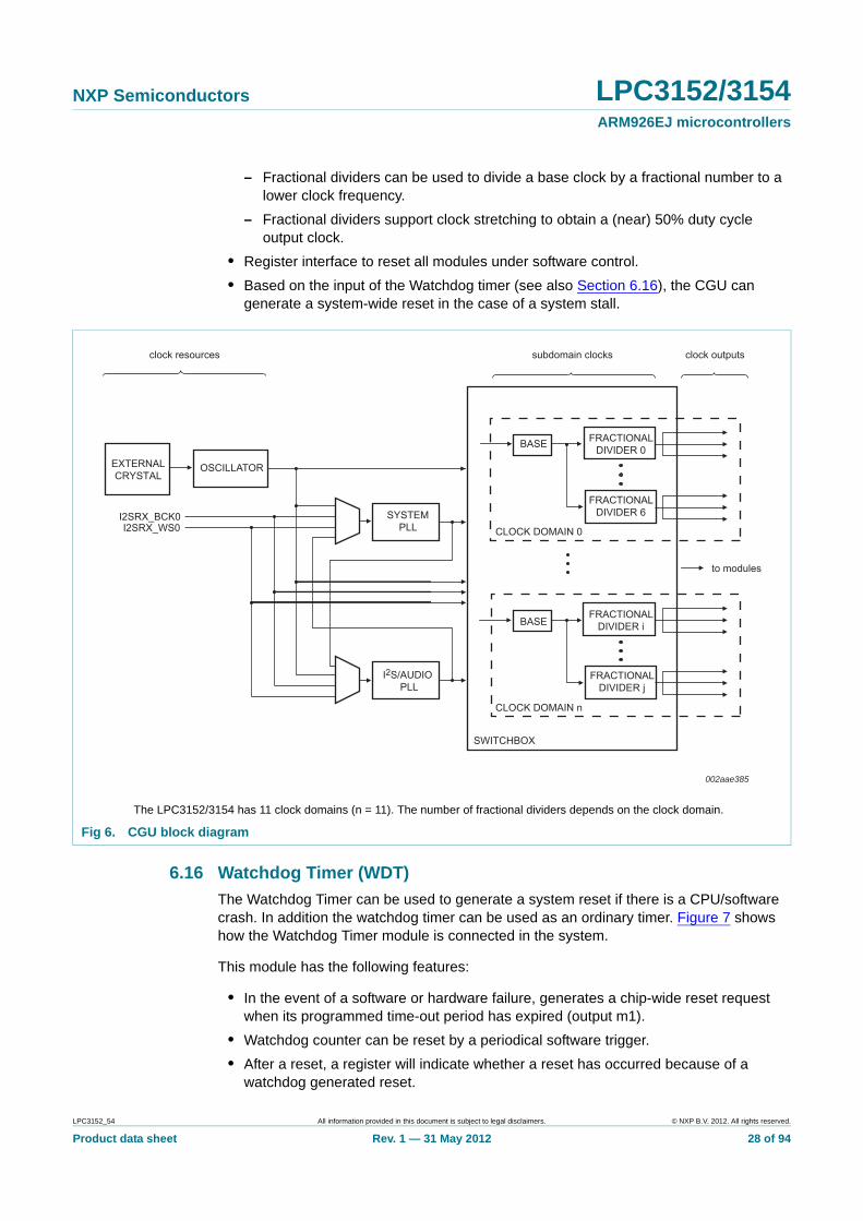
The structure of the CGU is shown in Figure 6. Each output clock generated by the CGU belongs to one of the domains. Each clock domain is fed by a single base clock that originates from one of the available clock sources. Within a clock domain, fractional dividers are available to divide the base clock to a lower frequency.
Within most clock domains, the output clocks are again grouped into one or more subdomains. All output clocks within one subdomain are either all generated by the same fractional divider or they are connected directly to the base clock. Therefore all output clocks within one subdomain have the same frequency and all output clocks within one clock domain are synchronous because they originate from the same base clock
The CGU reference clock is generated by the external crystal. Furthermore the CGU has several Phase Locked Loop (PLL) circuits to generate clock signals that can be used for system clocks and/or audio clocks. All clock sources, except the output of the PLLs, can be used as reference input for the PLLs.
This module has the following features:
• Advanced features to optimize the system for low power:
– All output clocks can be disabled individually for flexible power optimization
– Some modules have automatic clock gating: they are only active when (bus) access to the module is required.
– Variable clock scaling for automatic power optimization of the AHB bus (high clock frequency when the bus is active, low clock frequency when the bus is idle).
– Clock wake-up feature: module clocks can be programmed to be activated automatically on the basis of an event detected by the Event Router (see also Section 6.19). For example, all clocks (including the ARM /bus clocks) are off and activated automatically when a button is pressed.
• Supports three clock sources:
– Reference clock generated by the oscillator with an external crystal.
– Pins I2SRX_BCK0, I2SRX_WS0 are used to input external clock signals (used for generating audio frequencies in I2S receive / I2S transmit slave mode, see also Section 6.4).
• Two PLLs:
– System PLL generates programmable system clock frequency from its reference input.
– Audio PLL generates programmable audio clock frequency (typically 256 fs) from its reference input.
Remark: Both the System PLL and the audio PLL generate their frequencies based on their (individual) reference clocks. The reference clocks can be programmed to the oscillator clock or one of the external clock signals.
• Highly flexible switchbox to distribute the signals from the clock sources to the module clocks.
– Each clock generated by the CGU is derived from one of the base clocks and optionally divided by a fractional divider.
– Each base clock can be programmed to have any one of the clock sources as an input clock.
LPC3152_54 All information provided in this document is subject to legal disclaimers. © NXP B.V. 2012. All rights reserved.
Product data sheet Rev. 1 — 31 May 2012 27 of 94
NXP Semiconductors LPC3152/3154ARM926EJ microcontrollers
– Fractional dividers can be used to divide a base clock by a fractional number to a lower clock frequency.
– Fractional dividers support clock stretching to obtain a (near) 50% duty cycle output clock.
• Register interface to reset all modules under software control.
• Based on the input of the Watchdog timer (see also Section 6.16), the CGU can generate a system-wide reset in the case of a system stall.
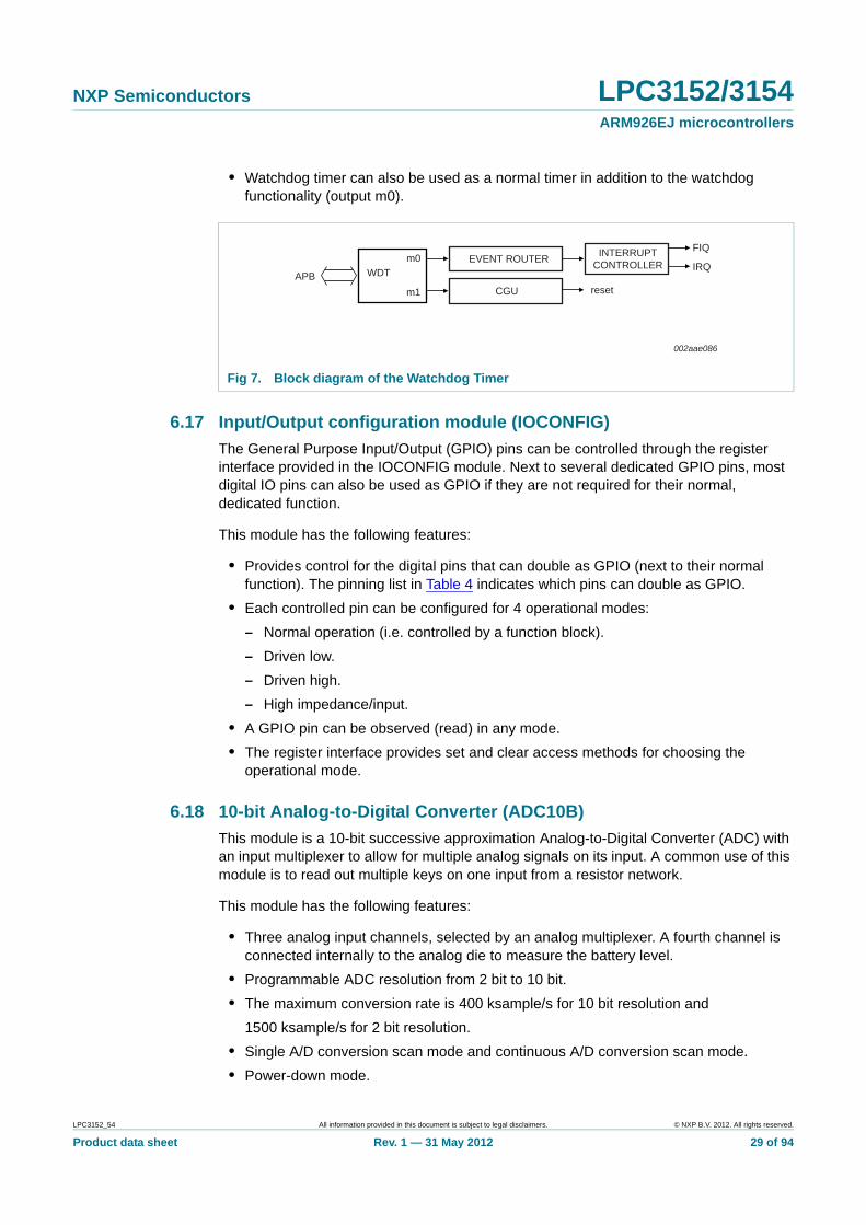
6.16 Watchdog Timer (WDT)
The Watchdog Timer can be used to generate a system reset if there is a CPU/software crash. In addition the watchdog timer can be used as an ordinary timer. Figure 7 shows how the Watchdog Timer module is connected in the system.
This module has the following features:
• In the event of a software or hardware failure, generates a chip-wide reset request when its programmed time-out period has expired (output m1).
• Watchdog counter can be reset by a periodical software trigger.
• After a reset, a register will indicate whether a reset has occurred because of a watchdog generated reset.
The LPC3152/3154 has 11 clock domains (n = 11). The number of fractional dividers depends on the clock domain.
Fig 6. CGU block diagram
OSCILLATOR
I2SRX_BCK0I2SRX_WS0
BASE
BASE
I2S/AUDIO PLL
EXTERNALCRYSTAL
SYSTEMPLL
002aae385
CLOCK DOMAIN 0
CLOCK DOMAIN n
FRACTIONALDIVIDER 0
FRACTIONALDIVIDER i
FRACTIONALDIVIDER 6
FRACTIONALDIVIDER j
clock resources clock outputs
SWITCHBOX
subdomain clocks
to modules
LPC3152_54 All information provided in this document is subject to legal disclaimers. © NXP B.V. 2012. All rights reserved.
Product data sheet Rev. 1 — 31 May 2012 28 of 94
NXP Semiconductors LPC3152/3154ARM926EJ microcontrollers
• Watchdog timer can also be used as a normal timer in addition to the watchdog functionality (output m0).
6.17 Input/Output configuration module (IOCONFIG)
The General Purpose Input/Output (GPIO) pins can be controlled through the register interface provided in the IOCONFIG module. Next to several dedicated GPIO pins, most digital IO pins can also be used as GPIO if they are not required for their normal, dedicated function.
This module has the following features:
• Provides control for the digital pins that can double as GPIO (next to their normal function). The pinning list in Table 4 indicates which pins can double as GPIO.
• Each controlled pin can be configured for 4 operational modes:
– Normal operation (i.e. controlled by a function block).
– Driven low.
– Driven high.
– High impedance/input.
• A GPIO pin can be observed (read) in any mode.
• The register interface provides set and clear access methods for choosing the operational mode.
6.18 10-bit Analog-to-Digital Converter (ADC10B)
This module is a 10-bit successive approximation Analog-to-Digital Converter (ADC) with an input multiplexer to allow for multiple analog signals on its input. A common use of this module is to read out multiple keys on one input from a resistor network.
This module has the following features:
• Three analog input channels, selected by an analog multiplexer. A fourth channel is connected internally to the analog die to measure the battery level.
• Programmable ADC resolution from 2 bit to 10 bit.
• The maximum conversion rate is 400 ksample/s for 10 bit resolution and
1500 ksample/s for 2 bit resolution.
• Single A/D conversion scan mode and continuous A/D conversion scan mode.
• Power-down mode.
Fig 7. Block diagram of the Watchdog Timer
002aae086
EVENT ROUTERWDT
m0
m1 CGU
INTERRUPTCONTROLLER
FIQ
IRQ
resetAPB
LPC3152_54 All information provided in this document is subject to legal disclaimers. © NXP B.V. 2012. All rights reserved.
Product data sheet Rev. 1 — 31 May 2012 29 of 94
NXP Semiconductors LPC3152/3154ARM926EJ microcontrollers
6.19 Event router
The event router extends the interrupt capability of the system by offering a flexible and versatile way of generating interrupts. Combined with the wake-up functionality of the CGU, it also offers a way to wake-up the system from suspend mode (with all clocks deactivated).
The event router has four interrupt outputs connected to the interrupt controller and one wake-up output connected to the CGU as shown in Figure 8. The output signals are activated when an event (for instance a rising edge) is detected on one of the input signals. The input signals of the event router are connected to relevant internal (control) signals in the system or to external signals through pins of the LPC3152/3154.
This module has the following features:
• Provides programmable routing of input events to multiple outputs for use as interrupts or wake up signals.
• Input events can come from internal signals or from the pins that can be used as GPIO.
• Inputs can be used either directly or latched (edge detected) as an event source.
• The active level (polarity) of the input signal for triggering events is programmable.
• Direct events will disappear when the input becomes inactive.
• Latched events will remain active until they are explicitly cleared.
• Each input can be masked globally for all inputs at once.
• Each input can be masked for each output individually.
• Event detect status can be read for each output separately.
• Event detection is fully asynchronous (no active clock required).
• Module can be used to generate a system wake-up from suspend mode.
Remark: All pins that can be used as GPIO are connected to the event router (see Figure 8). Note that they can be used to trigger events when in normal, functional mode or in GPIO mode.
Fig 8. Event router block diagram
002aae087
EVENT ROUTER
CGU
INTERRUPTCONTROLLER
interrupt 0
interrupt 1
interrupt 2
interrupt 3
cgu wakeup
APB
internalinput signals
external pins (GPIO configurable)
LPC3152_54 All information provided in this document is subject to legal disclaimers. © NXP B.V. 2012. All rights reserved.
Product data sheet Rev. 1 — 31 May 2012 30 of 94
NXP Semiconductors LPC3152/3154ARM926EJ microcontrollers
6.20 Random Number Generator (RNG)
The random number generator generates true random numbers for use in advanced security and Digital Rights Management (DRM) related schemes. These schemes rely upon truly random, i.e. completely unpredictable numbers.
This module has the following features:
• True random number generator.
• The random number register does not rely on any kind of reset.
• The generators are free running in order to ensure randomness and security.
6.21 AES decryption (LPC3154 only)
This module can be used for data decryption using the AES algorithm. The AES module has the following features:
• AES-128: 128 bit key, 128 bit data.
• CBC mode over blocks of 512 bytes.
• Each block of 512 bytes uses the same initial value.
• AES can be turned on and off.
6.22 Secure One-Time Programmable (OTP) memory
The OTP memory can be used for storing non-volatile information like serial number, security bits, etc. It consists of a polyfuse array, embedded data registers, and control registers. One of the main purposes of the OTP is storing a security key and a unique ID.
This module has the following features:
• 512-bit, one-time programmable memory
– 128 bit are used for an unique ID which is pre-programmed in the wafer fab.
– 40 bit are used for security and other features which are programmed at the customer production line.
– 184 bit are available for customer use.
– 32 bit are used for USB product ID and vendor ID by boot ROM in DFU mode.
– 128 bit are for the secure key used by boot ROM to load secure images.
Remark: On the LPC3152 secure boot is not supported hence these bits are also available for customer use.
• Programmable at the customer production line
• Random read access via sixteen 32-bit registers
• Flexible read protection mechanism to hide security related data
• Flexible write protection mechanism
6.23 Serial Peripheral Interface (SPI)
The SPI module is used for synchronous serial data communication with other devices which support the SPI/SSI protocol. Examples of the devices that this SPI module can communicate with are memories, cameras, and WiFi-g.
LPC3152_54 All information provided in this document is subject to legal disclaimers. © NXP B.V. 2012. All rights reserved.
Product data sheet Rev. 1 — 31 May 2012 31 of 94
NXP Semiconductors LPC3152/3154ARM926EJ microcontrollers
The SPI/SSI-bus is a 5-wire interface, and it is suitable for low, medium, and high data rate transfers.
This module has the following features:
• Supports Motorola SPI frame format with a word size of 8/16 bits.
• Texas Instruments SSI (Synchronous Serial Interface) frame format with a word size of 4 bit to 16 bit.
• Receive FIFO and transmit FIFO of 64 half-words each.
• Serial clock rate master mode maximum 45 MHz.
• Serial clock rate slave mode maximum 25 MHz.
• Support for single data access DMA.
• Full-duplex operation.
• Supports up to three slaves.
• Supports maskable interrupts.
• Supports DMA transfers.
6.24 Universal Asynchronous Receiver Transmitter (UART)
The UART module supports the industry standard serial interface.
This module has the following features:
• Programmable baud rate with a maximum of 1049 kBd.
• Programmable data length (5 bit to 8 bit).
• Implements only asynchronous UART.
• Transmit break character length indication.
• Programmable one to two stops bits in transmission.
• Odd/even/force parity check/generation.
• Frame error, overrun error and break detection.
• Automatic hardware flow control.
• Independent control of transmit, receive, line status, data set interrupts, and FIFOs.
• SIR-IrDA encoder/decoder (from 2400 to 115 kBd).
• Supports maskable interrupts.
• Supports DMA transfers.
6.25 Pulse Code Modulation (PCM) interface
The PCM interface supports the PCM and IOM interfaces.
This module has the following features:
• Four-wire serial interface.
• Can function in both Master and Slave modes.
• Supports:
– MP PCM (Multi-Protocol PCM): Configurable directional per slot.
LPC3152_54 All information provided in this document is subject to legal disclaimers. © NXP B.V. 2012. All rights reserved.
Product data sheet Rev. 1 — 31 May 2012 32 of 94
NXP Semiconductors LPC3152/3154ARM926EJ microcontrollers
– PCM (Pulse Code Modulation): Single clocking physical format.
– IOM-2 (Extended ISDN-Oriented modular): Double clocking physical format.
• Twelve 8 bit slots in a frame with enabling control per slot.
• Internal frame clock generation in master mode.
• Receive and transmit DMA handshaking using a request/clear protocol.
• Interrupt generation per frame.
PCM is a very common method used for transmitting analog data in digital format. Most common applications of PCM are digital audio as in audio CDs and computers, digital telephony, and digital videos.
The IOM (ISDN Oriented Modular) interface is primarily used to interconnect telecommunications ICs providing ISDN compatibility. It delivers a symmetrical full-duplex communication link containing user data, control/programming lines, and status channels.
6.26 LCD interface
The LCD interface contains logic to interface to a 6800 (Motorola) or 8080 (Intel) compatible LCD controller which supports 4/8/16 bit modes. This module also supports a serial interface mode. The speed of the interface can be adjusted in software to match the speed of the connected LCD display.
This module has the following features:
• 4/8/16 bit parallel interface mode: 6800-series, 8080-series.
• Serial interface mode.
• Supports multiple frequencies for the 6800/8080 bus to support high- and low-speed controllers.
• Supports polling the busy flag from LCD controller to off-load the CPU from polling.
• Contains an 16 byte FIFO for sending control and data information to the LCD controller.
• Supports maskable interrupts.
• Supports DMA transfers.
6.27 I2C-bus master/slave interface
The LPC3152/3154 contains two I2C master/slave interfaces. I2C-bus 0 can be used for communicating directly with I2C-compatible external devices. I2C-bus 1 is internally connected to support the following analog blocks: Li-ion charger, power supply unit, RTC, audio ADC, audio DAC, and class AB amplifier.
This module has the following features:
• I2C0 interface: I2C0 is a standard I2C-compliant bus interface with open-drain pins. This interface supports functions described in the I2C specification for speeds up to 400 kHz. This includes multi-master operation and allows powering off this device in a working system while leaving the I2C-bus functional.
• I2C1 interface: internally connected to control the functions on the analog die.
• Supports normal mode (100 kHz SCL).
LPC3152_54 All information provided in this document is subject to legal disclaimers. © NXP B.V. 2012. All rights reserved.
Product data sheet Rev. 1 — 31 May 2012 33 of 94
NXP Semiconductors LPC3152/3154ARM926EJ microcontrollers
• Fast mode (400 kHz SCL with 24 MHz APB clock; 325 kHz with12 MHz APB clock; 175 kHz with 6 MHz APB clock).
• Interrupt support.
• Supports DMA transfers (single).
• Four modes of operation:
– Master transmitter
– Master receiver
– Slave transmitter
– Slave receiver
6.28 LCD/NAND flash/SDRAM multiplexing
The LPC3152/3154 contains a rich set of specialized hardware interfaces, but the TFBGA package does not contain enough pins to allow use of all signals of all interfaces simultaneously. Therefore a pin-multiplexing scheme is implemented, which allows the selection of the right interface for the application.
Pin multiplexing is enabled between the following interfaces:
• between the dedicated LCD interface and the External Bus Interface (EBI).
• between the NAND flash controller and the Memory Card Interface (MCI).
• between UART and SPI.
• between I2STX_0 output and the PCM interface.
The pin interface multiplexing is subdivided into five categories: storage, video, audio, NAND flash, and UART related pin multiplexing. Each category supports several modes, which can be selected by programming the corresponding registers in the SysCReg.
6.28.1 Pin connections
Table 11. Pin descriptions of multiplexed pins
Pin name Default signal Alternate signal Description
Video related pin multiplexing
mLCD_CSB LCD_CSB EBI_NSTCS_0 LCD_CSB — LCD chip select for external LCD controller.
EBI_NSTCS_0 — EBI static memory chip select 0.
mLCD_DB_1 LCD_DB_1 EBI_NSTCS_1 LCD_DB_1 — LCD bidirectional data line 1.
EBI_NSTCS_1 — EBI static memory chip select 1.
mLCD_DB_0 LCD_DB_0 EBI_CLKOUT LCD_DB_0 — LCD bidirectional data line 0.
EBI_CLKOUT — EBI SDRAM clock signal.
mLCD_E_RD LCD_E_RD EBI_CKE LCD_E_RD — LCD enable/read signal.
EBI_CKE — EBI SDRAM clock enable.
mLCD_RS LCD_RS EBI_NDYCS LCD_RS — LCD register select signal.
EBI_NDYCS — EBI SDRAM chip select.
mLCD_RW_WR LCD_RW_WR EBI_DQM_1 LCD_RW_WR — LCD read write/write signal.
EBI_DQM_1 — EBI SDRAM data mask output 1.
mLCD_DB_2 LCD_DB_2 EBI_A_2 LCD_DB_2 — LCD bidirectional data line 2.
EBI_A_2 — EBI address line 2.
LPC3152_54 All information provided in this document is subject to legal disclaimers. © NXP B.V. 2012. All rights reserved.
Product data sheet Rev. 1 — 31 May 2012 34 of 94
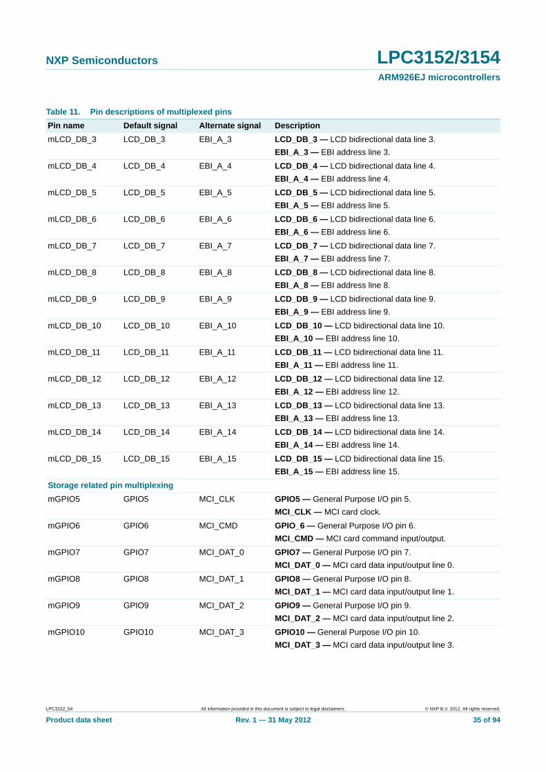
NXP Semiconductors LPC3152/3154ARM926EJ microcontrollers
mLCD_DB_3 LCD_DB_3 EBI_A_3 LCD_DB_3 — LCD bidirectional data line 3.
EBI_A_3 — EBI address line 3.
mLCD_DB_4 LCD_DB_4 EBI_A_4 LCD_DB_4 — LCD bidirectional data line 4.
EBI_A_4 — EBI address line 4.
mLCD_DB_5 LCD_DB_5 EBI_A_5 LCD_DB_5 — LCD bidirectional data line 5.
EBI_A_5 — EBI address line 5.
mLCD_DB_6 LCD_DB_6 EBI_A_6 LCD_DB_6 — LCD bidirectional data line 6.
EBI_A_6 — EBI address line 6.
mLCD_DB_7 LCD_DB_7 EBI_A_7 LCD_DB_7 — LCD bidirectional data line 7.
EBI_A_7 — EBI address line 7.
mLCD_DB_8 LCD_DB_8 EBI_A_8 LCD_DB_8 — LCD bidirectional data line 8.
EBI_A_8 — EBI address line 8.
mLCD_DB_9 LCD_DB_9 EBI_A_9 LCD_DB_9 — LCD bidirectional data line 9.
EBI_A_9 — EBI address line 9.
mLCD_DB_10 LCD_DB_10 EBI_A_10 LCD_DB_10 — LCD bidirectional data line 10.
EBI_A_10 — EBI address line 10.
mLCD_DB_11 LCD_DB_11 EBI_A_11 LCD_DB_11 — LCD bidirectional data line 11.
EBI_A_11 — EBI address line 11.
mLCD_DB_12 LCD_DB_12 EBI_A_12 LCD_DB_12 — LCD bidirectional data line 12.
EBI_A_12 — EBI address line 12.
mLCD_DB_13 LCD_DB_13 EBI_A_13 LCD_DB_13 — LCD bidirectional data line 13.
EBI_A_13 — EBI address line 13.
mLCD_DB_14 LCD_DB_14 EBI_A_14 LCD_DB_14 — LCD bidirectional data line 14.
EBI_A_14 — EBI address line 14.
mLCD_DB_15 LCD_DB_15 EBI_A_15 LCD_DB_15 — LCD bidirectional data line 15.
EBI_A_15 — EBI address line 15.
Storage related pin multiplexing
mGPIO5 GPIO5 MCI_CLK GPIO5 — General Purpose I/O pin 5.
MCI_CLK — MCI card clock.
mGPIO6 GPIO6 MCI_CMD GPIO_6 — General Purpose I/O pin 6.
MCI_CMD — MCI card command input/output.
mGPIO7 GPIO7 MCI_DAT_0 GPIO7 — General Purpose I/O pin 7.
MCI_DAT_0 — MCI card data input/output line 0.
mGPIO8 GPIO8 MCI_DAT_1 GPIO8 — General Purpose I/O pin 8.
MCI_DAT_1 — MCI card data input/output line 1.
mGPIO9 GPIO9 MCI_DAT_2 GPIO9 — General Purpose I/O pin 9.
MCI_DAT_2 — MCI card data input/output line 2.
mGPIO10 GPIO10 MCI_DAT_3 GPIO10 — General Purpose I/O pin 10.
MCI_DAT_3 — MCI card data input/output line 3.
Table 11. Pin descriptions of multiplexed pins
Pin name Default signal Alternate signal Description
LPC3152_54 All information provided in this document is subject to legal disclaimers. © NXP B.V. 2012. All rights reserved.
Product data sheet Rev. 1 — 31 May 2012 35 of 94
NXP Semiconductors LPC3152/3154ARM926EJ microcontrollers
6.28.2 Multiplexing between LCD and MPMC
The multiplexing between the LCD interface and MPMC allows for the following two modes of operation:
• MPMC-mode: SDRAM and bus-based LCD or SRAM.
• LCD-mode: Dedicated LCD-Interface.
The external NAND flash is accessible in both modes.
The block diagram Figure 9 gives a high level overview of the modules in the chip that are involved in the pin interface multiplexing between the EBI, NAND flash controller, MPMC, and RAM-based LCD interface.
NAND flash related pin multiplexing
mNAND_RYBN0 NAND_RYBN0 MCI_DAT_4 NAND_RYBN0 — NAND flash controller Read/Not busy signal 0.
MCI_DAT_4 — MCI card data input/output line 4.
mNAND_RYBN1 NAND_RYBN1 MCI_DAT_5 NAND_RYBN1 — NAND flash controller Read/Not busy signal 1.
MCI_DAT_5 — MCI card data input/output line 5.
mNAND_RYBN2 NAND_RYBN2 MCI_DAT_6 NAND_RYBN2 — NAND flash controller Read/Not busy signal 2.
MCI_DAT_6 — MCI card data input/output line 6.
mNAND_RYBN3 NAND_RYBN3 MCI_DAT_7 NAND_RYBN3 — NAND flash controller Read/Not busy signal 3.
MCI_DAT_7 — MCI card data input/output line 7.
Audio related pin multiplexing
mI2STX_DATA0 I2STX_DATA0 PCM_DA I2STX_DATA0 — I2S interface 0 transmit data signal.
PCM_DA — PCM serial data line A.
mI2STX_BCK0 I2STX_BCK0 PCM_FSC I2STX_BCK0 — I2S interface 0 transmit bitclock signal.
PCM_FSC — PCM frame synchronization signal.
mI2STX_WS0 I2STX_WS0 PCM_DCLK I2STX_WS0 — I2S interface 0 transmit word select signal.
PCM_DCLK — PCM data clock output.
mI2STX_CLK0 I2STX_CLK0 PCM_DB I2STX_CLK0 — I2S interface 0 transmit clock signal.
PCM_DB — PCM serial data line B.
UART related pin multiplexing
mUART_CTS_N UART_CTS_N SPI_CS_OUT1 UART_CTS_N — UART modem control Clear-to-Send signal.
SPI_CS_OUT1 — SPI chip select out for slave 1 (used in master mode).
mUART_RTS_N UART_RTS_N SPI_CS_OUT2 UART_RTS_N — UART modem control Request-to-Send signal.
SPI_CS_OUT2 — SPI chip select out for slave 2 (used in master mode).
Table 11. Pin descriptions of multiplexed pins
Pin name Default signal Alternate signal Description
LPC3152_54 All information provided in this document is subject to legal disclaimers. © NXP B.V. 2012. All rights reserved.
Product data sheet Rev. 1 — 31 May 2012 36 of 94
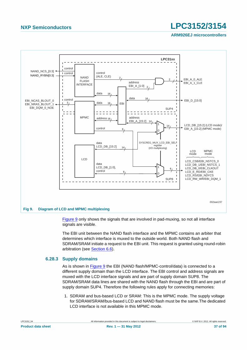
NXP Semiconductors LPC3152/3154ARM926EJ microcontrollers
Figure 9 only shows the signals that are involved in pad-muxing, so not all interface signals are visible.
The EBI unit between the NAND flash interface and the MPMC contains an arbiter that determines which interface is muxed to the outside world. Both NAND flash and SDRAM/SRAM initiate a request to the EBI unit. This request is granted using round-robin arbitration (see Section 6.6).
6.28.3 Supply domains
As is shown in Figure 9 the EBI (NAND flash/MPMC-control/data) is connected to a different supply domain than the LCD interface. The EBI control and address signals are muxed with the LCD interface signals and are part of supply domain SUP8. The SDRAM/SRAM data lines are shared with the NAND flash through the EBI and are part of supply domain SUP4. Therefore the following rules apply for connecting memories:
1. SDRAM and bus-based LCD or SRAM: This is the MPMC mode. The supply voltage for SDRAM/SRAM/bus-based LCD and NAND flash must be the same.The dedicated LCD interface is not available in this MPMC mode.
Fig 9. Diagram of LCD and MPMC multiplexing
NAND_RYBN[0:3]NAND_NCS_[0:3]
NANDFLASH
INTERFACE
control
control
control
dataLCD_DB_[1:0],control
control control(ALE, CLE)
EBI_A_0_ALEEBI_A_1_CLE
EBI
2
16data
2
6
data 16
addressEBI_A_[15:2] 14
14
dataLCD_DB_[15:2] 14
6
EBI_NCAS_BLOUT_0EBI_NRAS_BLOUT_1
EBI_DQM_0_NOE
LCD_CSB/EBI_NSTCS_0 LCD_DB_1/EBI_NSTCS_1 LCD_DB_0/EBI_CLKOUT LCD_E_RD/EBI_CKELCD_RS/EBI_NDYCS LCD_RW_WR/EBI_DQM_1
LCD_DB_[15:2] (LCD mode)/EBI_A_[15:2] (MPMC mode)
EBI_D_[15:0]16data
16addressMPMC
LCD
addressEBI_A_[1:0]
2
6
3
SYSCREG_MUX_LCD_EBI_SEL register
(I/O multplexing)MPMCmode
LCDmode
LPC31xx
002aae157
SUP4
SUP8
0
1
0
1
LPC3152_54 All information provided in this document is subject to legal disclaimers. © NXP B.V. 2012. All rights reserved.
Product data sheet Rev. 1 — 31 May 2012 37 of 94
NXP Semiconductors LPC3152/3154ARM926EJ microcontrollers
2. Dedicated LCD interface only: This is the LCD mode. The NAND flash supply voltage (SUP4) can be different from the LCD supply voltage (SUP8).
6.29 Timer module
The LPC3152/3154 contains four fully independent timer modules, which can be used to generate interrupts after a pre-set time interval has elapsed.
This module has the following features:
• Each timer is a 32 bit wide down-counter with selectable pre-scale. The pre-scaler allows using either the module clock directly or the clock divided by 16 or 256.
• Two modes of operation:
– Free-running timer: The timer generates an interrupt when the counter reaches zero. The timer wraps around to 0xFFFF FFFF and continues counting down.
– Periodic timer: The timer generates an interrupt when the counter reaches zero. It reloads the value from a load register and continues counting down from that value. An interrupt will be generated every time the counter reaches zero. This effectively gives a repeated interrupt at a regular interval.
• At any time the current timer value can be read.
• At any time the value in the load register may be re-written, causing the timer to restart.
6.30 Pulse Width Modulation (PWM) module
This PWM can be used to generate a pulse width modulated or a pulse density modulated signal. With an external low pass filter, the module can be used to generate a low frequent analog signal. A typical use of the output of the module is to control the backlight of an LCD display.
This module has the following features:
• Supports Pulse Width Modulation (PWM) with software controlled duty cycle.
• Supports Pulse Density Modulation (PDM) with software controlled pulse density.
6.31 System control registers
The System Control Registers (SysCReg) module provides a register interface for some of the high-level settings in the system such as multiplexers and mode settings. This is an auxiliary module included in this overview for the sake of completeness.
6.32 Audio Subsystem (ADSS)
The audio subsystem consists of the following blocks:
• I2S interfaces on the digital die (see Section 6.32.1):
– I2S0 digital audio input/output (I2SRX_0/I2STX_0)
– I2S1 (I2SRX_1/I2STX_1) interface to the audio analog block (I2S1 signals not pinned out)
– Edge detector
LPC3152_54 All information provided in this document is subject to legal disclaimers. © NXP B.V. 2012. All rights reserved.
Product data sheet Rev. 1 — 31 May 2012 38 of 94
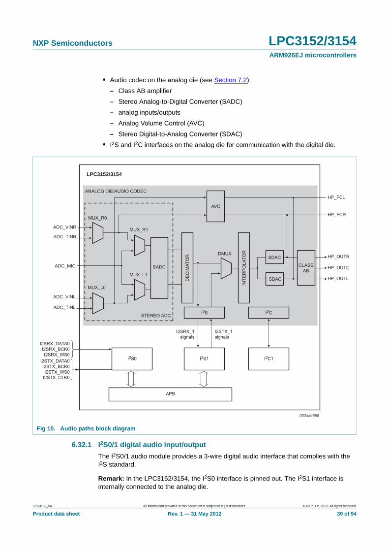
NXP Semiconductors LPC3152/3154ARM926EJ microcontrollers
• Audio codec on the analog die (see Section 7.2):
– Class AB amplifier
– Stereo Analog-to-Digital Converter (SADC)
– analog inputs/outputs
– Analog Volume Control (AVC)
– Stereo Digital-to-Analog Converter (SDAC)
• I2S and I2C interfaces on the analog die for communication with the digital die.
6.32.1 I2S0/1 digital audio input/output
The I2S0/1 audio module provides a 3-wire digital audio interface that complies with the I2S standard.
Remark: In the LPC3152/3154, the I2S0 interface is pinned out. The I2S1 interface is internally connected to the analog die.
Fig 10. Audio paths block diagram
DE
CIM
ATO
R
INTE
RP
OLA
TOR
CLASSAB
LPC3152/3154
HP_FCL
HP_FCR
HP_OUTR
HP_OUTL
I2S1 I2C1
I2CI2S
I2S0
HP_OUTC
DMUX
MUX_R1
MUX_R0
MUX_L0
SDAC
SDAC
AVC
I2STX_1signals
I2SRX_1signals
I2STX_DATA0I2STX_BCK0I2STX_WS0
I2STX_CLK0
ADC_MIC
ADC_VINL
ADC_TINL
I2SRX_DATA0I2SRX_BCK0I2SRX_WS0
MUX_L1
ADC_VINR
ADC_TINR
STEREO ADC
SADC
ANALOG DIE/AUDIO CODEC
002aae558
APB
LPC3152_54 All information provided in this document is subject to legal disclaimers. © NXP B.V. 2012. All rights reserved.
Product data sheet Rev. 1 — 31 May 2012 39 of 94
NXP Semiconductors LPC3152/3154ARM926EJ microcontrollers
The I2S0/1 module has the following features:
• Receive input supports master mode and slave mode.
• Transmit output supports master mode.
• Supports LSB justified words of 16, 18, 20 and 24 bits.
• Supports a configurable number of bit clock periods per word select period (up to 128 bit clock periods).
• Supports DMA transfers.
• Transmit FIFO or receive FIFO of 4 stereo samples.
• Supports single 16-bit transfers to/from the left or right FIFO.
• Supports single 24-bit transfers to/from the left or right FIFO.
• Supports 32-bit interleaved transfers, with the lower 16 bits representing the left audio sample and the higher 16 bits representing the right audio sample.
• Supports two 16-bit samples audio samples combined in a 32-bit word (2 left or 2 right samples) to reduce bus load.
• Provides maskable interrupts for audio status. (FIFO underrun/overrun/full/half_full/not empty for left and right channel separately).
7. Functional description of the analog die blocks
7.1 Analog die
The analog die part of the LPC3152/3154 contains the audio codec, the Real-Time Clock (RTC), the Power Supply Unit (PSU), the Li-ion charger, and the USB charge pump.
LPC3152_54 All information provided in this document is subject to legal disclaimers. © NXP B.V. 2012. All rights reserved.
Product data sheet Rev. 1 — 31 May 2012 40 of 94
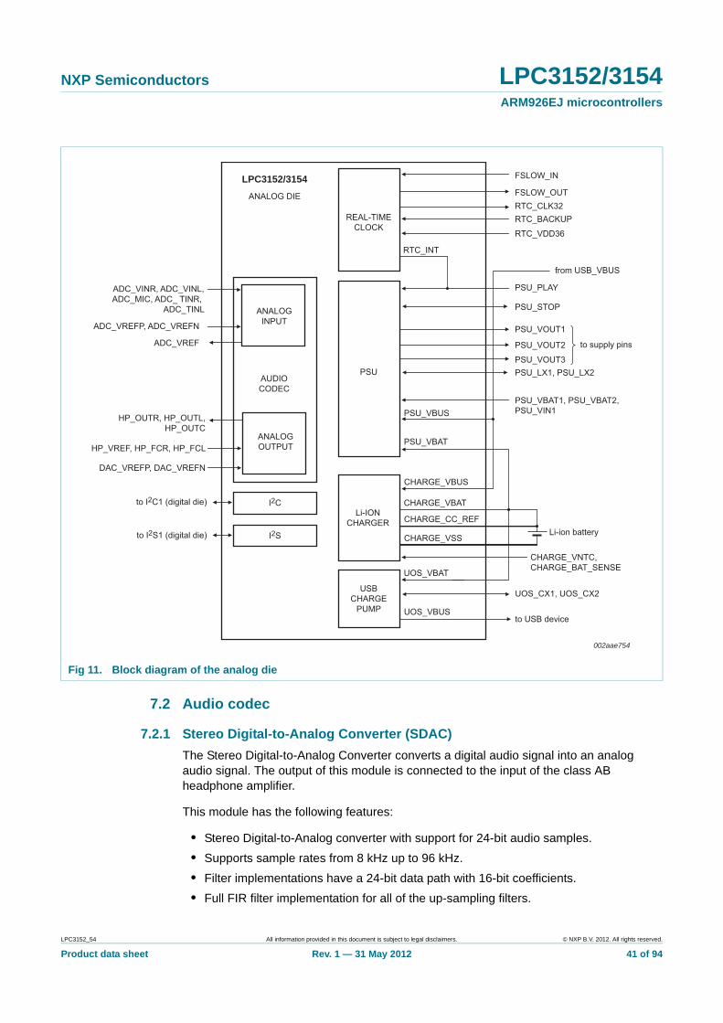
NXP Semiconductors LPC3152/3154ARM926EJ microcontrollers
7.2 Audio codec
7.2.1 Stereo Digital-to-Analog Converter (SDAC)
The Stereo Digital-to-Analog Converter converts a digital audio signal into an analog audio signal. The output of this module is connected to the input of the class AB headphone amplifier.
This module has the following features:
• Stereo Digital-to-Analog converter with support for 24-bit audio samples.
• Supports sample rates from 8 kHz up to 96 kHz.
• Filter implementations have a 24-bit data path with 16-bit coefficients.
• Full FIR filter implementation for all of the up-sampling filters.
Fig 11. Block diagram of the analog die
from USB_VBUS
PSU_VBAT1, PSU_VBAT2,PSU_VIN1
PSU_VBAT
PSU_VBUS
CHARGE_VBUS
PSU_VOUT1
PSU_STOP
PSU_PLAY
PSU_VOUT2
PSU_VOUT3PSU_LX1, PSU_LX2
to USB device
CHARGE_VBAT
PSUAUDIOCODEC
I2C
USBCHARGE
PUMP
REAL-TIMECLOCK
Li-IONCHARGER
I2S
ADC_VINR, ADC_VINL,ADC_MIC, ADC_ TINR,
ADC_TINL
ADC_VREFP, ADC_VREFN
ADC_VREF
ANALOGINPUT
ANALOGOUTPUT
HP_OUTR, HP_OUTL,HP_OUTC
HP_VREF, HP_FCR, HP_FCL
DAC_VREFP, DAC_VREFN
to I2C1 (digital die)
to I2S1 (digital die)
CHARGE_CC_REF
CHARGE_VSS
CHARGE_VNTC, CHARGE_BAT_SENSE
UOS_VBUS
UOS_CX1, UOS_CX2
UOS_VBAT
FSLOW_IN
FSLOW_OUT
RTC_INT
RTC_CLK32RTC_BACKUP
RTC_VDD36
LPC3152/3154
to supply pins
Li-ion battery
002aae754
ANALOG DIE
LPC3152_54 All information provided in this document is subject to legal disclaimers. © NXP B.V. 2012. All rights reserved.
Product data sheet Rev. 1 — 31 May 2012 41 of 94
NXP Semiconductors LPC3152/3154ARM926EJ microcontrollers
• Controlled power down sequence comprising a raised cosine mute function followed by a DC ramp down to zero to avoid audible plops or clicks.
• Digital dB-linear volume control in 0.25 dB steps.
• Digital de-emphasis for 32 kHz, 44.1 kHz, 48 kHz, and 96 kHz.
• Selection for the up-sampling filter characteristics (sharp/slow roll-off).
• Support for 2fs and 8fs input signals.
• Soft mute with a raised cosine function.
7.2.2 Class AB headphone amplifier
The class AB headphone amplifier amplifies an analog input signal to levels appropriate for a headphone output. Its input can be chosen from the Stereo Digital-to-Analog Converter (SADC) or from the analog bypass from the tuner input (through the Analog Volume Control (AVC) block). The class AB amplifier offers a solution in cases where high output levels are required or when the headphone wire is also used as an antenna for tuner reception.
This module has the following features:
• Stereo headphone amplifier.
• Three outputs: left, right, and a common signal ground output.
• Common signal ground output enables DC coupling of headphone without electrolytic capacitors.
• 16 and higher output drive capability.
• Individual power down modes for each output.
• Programmable short-circuit current protection for each amplifier.
• Additional input with Analog Volume Control (AVC) directly connected to the tuner input pins.
7.2.3 Stereo Analog-to-Digital Converter (SADC) for Audio
The Stereo ADC can convert analog audio input signals into digital audio signals as shown in Figure 12. The module has three input signals: stereo line-in (ADC_VINL/ADC_VINR), stereo tuner-in (ADC_TINL/ADC_TINR), and mono microphone in (ADC_MIC). These signals can be pre-processed by a Low-Noise Amplifier (LNA, microphone input only), a Programmable Gain Amplifier (PGA), and a Single-to-Differential Converter (SDC) before they arrive at the input of the actual SADC.
LPC3152_54 All information provided in this document is subject to legal disclaimers. © NXP B.V. 2012. All rights reserved.
Product data sheet Rev. 1 — 31 May 2012 42 of 94
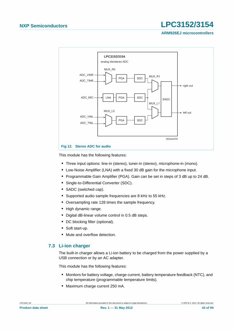
NXP Semiconductors LPC3152/3154ARM926EJ microcontrollers
This module has the following features:
• Three input options: line-in (stereo), tuner-in (stereo), microphone-in (mono).
• Low-Noise Amplifier (LNA) with a fixed 30 dB gain for the microphone input.
• Programmable Gain Amplifier (PGA). Gain can be set in steps of 3 dB up to 24 dB.
• Single-to-Differential Converter (SDC).
• SADC (switched cap).
• Supported audio sample frequencies are 8 kHz to 55 kHz.
• Oversampling rate 128 times the sample frequency.
• High dynamic range.
• Digital dB-linear volume control in 0.5 dB steps.
• DC blocking filter (optional).
• Soft start-up.
• Mute and overflow detection.
7.3 Li-ion charger
The built-in charger allows a Li-ion battery to be charged from the power supplied by a USB connection or by an AC adapter.
This module has the following features:
• Monitors for battery voltage, charge current, battery temperature feedback (NTC), and chip temperature (programmable temperature limits).
• Maximum charge current 250 mA.
Fig 12. Stereo ADC for audio
LNA PGA
PGA
PGA
SDC
SDC
SDC
LPC3152/3154
MUX_R1
MUX_R0
MUX_L0
ADC_VINR
ADC_TINR
ADC_MIC
ADC_VINL
ADC_TINL
MUX_L1SADC
right out
left out
002aae559
analog die/stereo ADC
LPC3152_54 All information provided in this document is subject to legal disclaimers. © NXP B.V. 2012. All rights reserved.
Product data sheet Rev. 1 — 31 May 2012 43 of 94
NXP Semiconductors LPC3152/3154ARM926EJ microcontrollers
• The nominal charge current is programmed with an external program-resistor. This allows the charge current to be adapted to the USB enumeration.
• Uses a widespread method to charge a Li-ion battery with the following stages:
– Trickle charging with a small current for an (almost) empty battery.
– Fast charging in Constant Current mode (CC mode) to the maximum battery voltage of 4.2 V 1%.
– Switch from CC mode to Constant Voltage charging (CV mode) keeping the battery voltage at 4.2 V and monitoring the current for ending the charge process.
• Short circuit resistant.
• Charger state can be observed through a register.
7.4 USB charge pump (host mode)
The USB charge pump uses the Li-ion battery to provide a low-power USB VBUS signal for the USB controller in host mode.
7.5 Power Supply Unit (PSU)
The integrated PSU allows the system to run directly from the battery voltage or the USB power supply voltage USB_VBUS. It converts the battery voltage or the USB_VBUS voltage into the supply voltages required for both the digital and analog blocks in the rest of the system.
LPC3152_54 All information provided in this document is subject to legal disclaimers. © NXP B.V. 2012. All rights reserved.
Product data sheet Rev. 1 — 31 May 2012 44 of 94
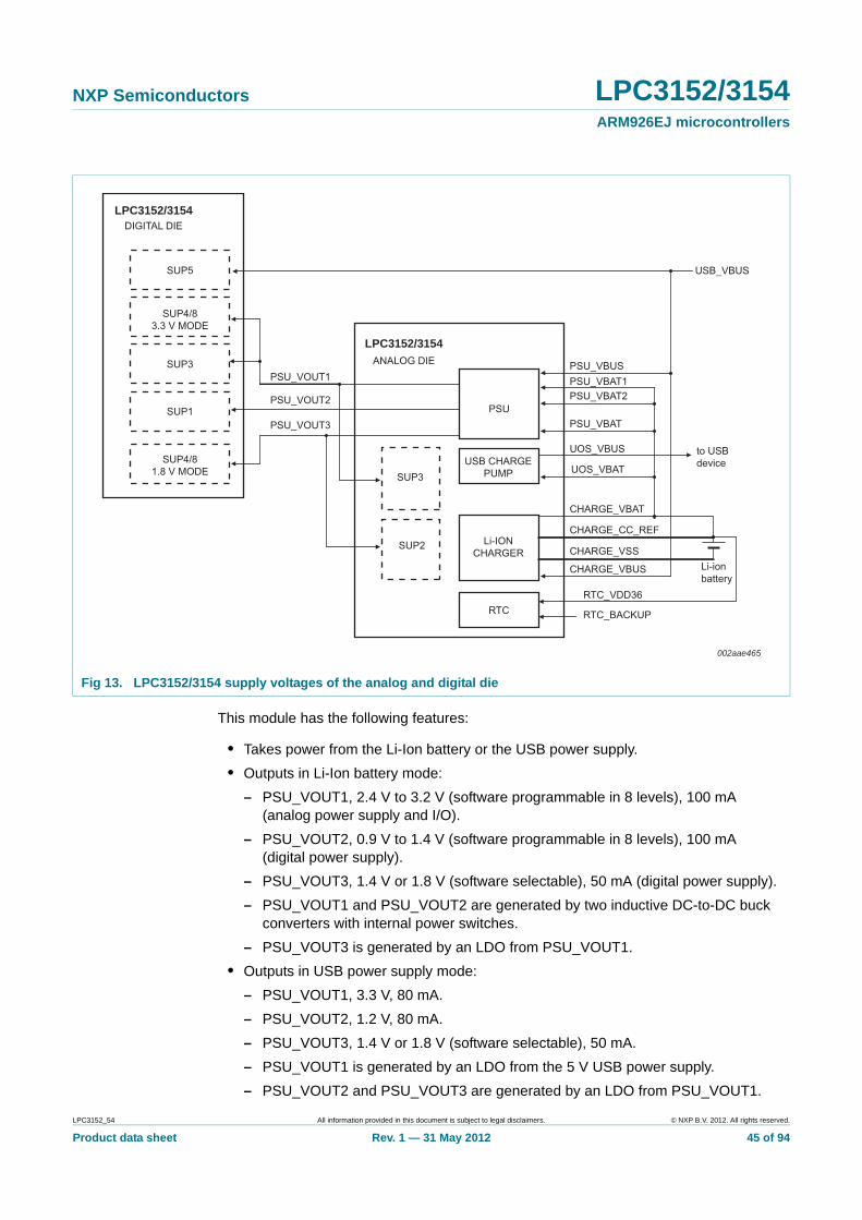
NXP Semiconductors LPC3152/3154ARM926EJ microcontrollers
This module has the following features:
• Takes power from the Li-Ion battery or the USB power supply.
• Outputs in Li-Ion battery mode:
– PSU_VOUT1, 2.4 V to 3.2 V (software programmable in 8 levels), 100 mA (analog power supply and I/O).
– PSU_VOUT2, 0.9 V to 1.4 V (software programmable in 8 levels), 100 mA (digital power supply).
– PSU_VOUT3, 1.4 V or 1.8 V (software selectable), 50 mA (digital power supply).
– PSU_VOUT1 and PSU_VOUT2 are generated by two inductive DC-to-DC buck converters with internal power switches.
– PSU_VOUT3 is generated by an LDO from PSU_VOUT1.
• Outputs in USB power supply mode:
– PSU_VOUT1, 3.3 V, 80 mA.
– PSU_VOUT2, 1.2 V, 80 mA.
– PSU_VOUT3, 1.4 V or 1.8 V (software selectable), 50 mA.
– PSU_VOUT1 is generated by an LDO from the 5 V USB power supply.
– PSU_VOUT2 and PSU_VOUT3 are generated by an LDO from PSU_VOUT1.
Fig 13. LPC3152/3154 supply voltages of the analog and digital die
PSU_VOUT2
PSU_VOUT1
PSU_VOUT3
USB_VBUS
PSU
PSU_VBUS
PSU_VBAT
PSU_VBAT1
RTC_BACKUP
RTC_VDD36
PSU_VBAT2
UOS_VBAT
UOS_VBUS
CHARGE_VBUS
Li-IONCHARGER
USB CHARGEPUMP
LPC3152/3154
LPC3152/3154
002aae465
SUP3
SUP5
SUP4/83.3 V MODE
SUP4/81.8 V MODE
SUP1
SUP3
SUP2
to USBdevice
CHARGE_VBAT
CHARGE_CC_REF
CHARGE_VSSLi-ionbattery
RTC
ANALOG DIE
DIGITAL DIE
LPC3152_54 All information provided in this document is subject to legal disclaimers. © NXP B.V. 2012. All rights reserved.
Product data sheet Rev. 1 — 31 May 2012 45 of 94
NXP Semiconductors LPC3152/3154ARM926EJ microcontrollers
• Provides ‘Supply_OK’ detection connected to the system reset signal.
7.6 Real-Time Clock (RTC)
The Real-Time Clock module keeps track of the actual date and time, also when the system is switched off. Advanced Digital Rights Management (DRM) schemes require a secure and accurate real-time clock for managing rights such as time-limited playback rights.
This module has the following features:
• Normal power supply directly from Li-ion battery (PSU is by-passed).
• Backup power supply from (external) capacitor.
• Automatic switching between normal power supply and backup power supply.
• Signals power loss to indicate invalid real time clock readings.
• Runs on a 32 kHz oscillator.
• Ultra-low power consumption.
• The clock is implemented as a 32-bit counter at the rate of 1 Hz (derived from the 32 kHz clock).
• Alarm timer that can generate an interrupt. This interrupt is available both as an internal signal as well as a signal on an external pin.
• The external interrupt (RTC_INT) can be used to switch on the system by switching on the PSU through the PSU_PLAY pin.
• The internal interrupt signal can be used to wake-up the system from suspend mode through the event router.
• Dedicated permanent supply domain.
LPC3152_54 All information provided in this document is subject to legal disclaimers. © NXP B.V. 2012. All rights reserved.
Product data sheet Rev. 1 — 31 May 2012 46 of 94
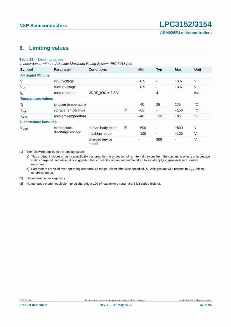
NXP Semiconductors LPC3152/3154ARM926EJ microcontrollers
8. Limiting values
[1] The following applies to the limiting values:
a) This product includes circuitry specifically designed for the protection of its internal devices from the damaging effects of excessive static charge. Nonetheless, it is suggested that conventional precautions be taken to avoid applying greater than the rated maximum.
b) Parameters are valid over operating temperature range unless otherwise specified. All voltages are with respect to VSS unless otherwise noted.
[2] Dependent on package type.
[3] Human body model: equivalent to discharging a 100 pF capacitor through a 1.5 k series resistor.
Table 12. Limiting valuesIn accordance with the Absolute Maximum Rating System (IEC 60134).[1]
Symbol Parameter Conditions Min Typ Max Unit
All digital I/O pins
VI input voltage 0.5 - +3.6 V
VO output voltage 0.5 - +3.6 V
IO output current VDDE_IOC = 3.3 V - 4 - mA
Temperature values
Tj junction temperature 40 25 125 C
Tstg storage temperature [2] 65 - +150 C
Tamb ambient temperature 40 +25 +85 C
Electrostatic handling
VESD electrostatic discharge voltage
human body model [3] 500 - +500 V
machine model 100 - +100 V
charged device model
- 500 - V
LPC3152_54 All information provided in this document is subject to legal disclaimers. © NXP B.V. 2012. All rights reserved.
Product data sheet Rev. 1 — 31 May 2012 47 of 94
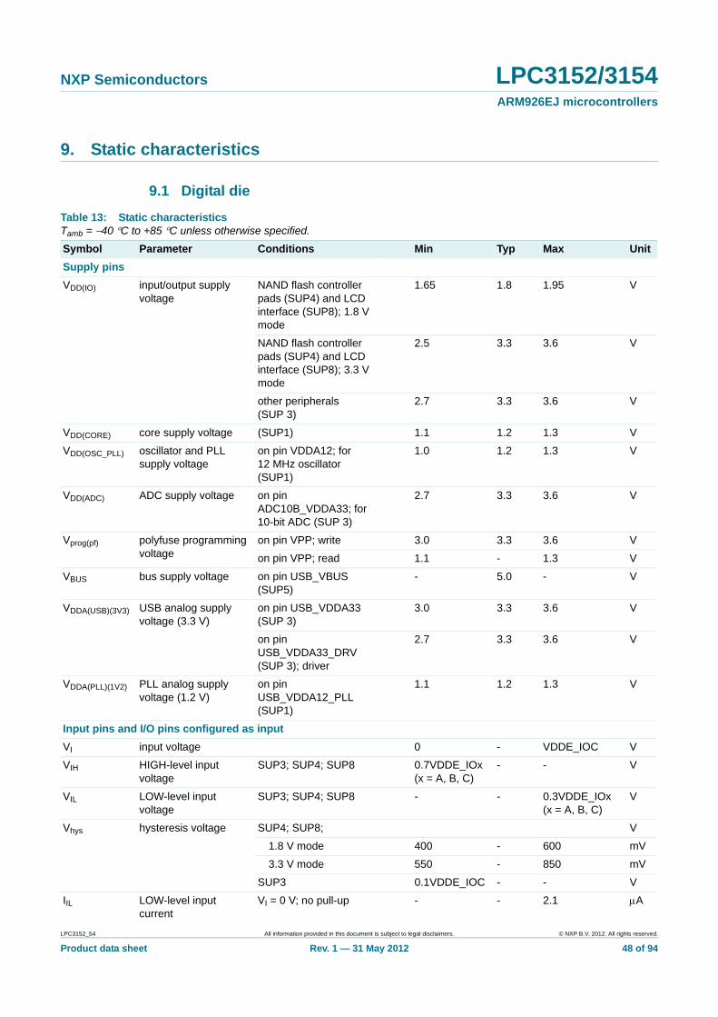
NXP Semiconductors LPC3152/3154ARM926EJ microcontrollers
9. Static characteristics
9.1 Digital die
Table 13: Static characteristicsTamb = 40 C to +85 C unless otherwise specified.
Symbol Parameter Conditions Min Typ Max Unit
Supply pins
VDD(IO) input/output supply voltage
NAND flash controller pads (SUP4) and LCD interface (SUP8); 1.8 V mode
1.65 1.8 1.95 V
NAND flash controller pads (SUP4) and LCD interface (SUP8); 3.3 V mode
2.5 3.3 3.6 V
other peripherals (SUP 3)
2.7 3.3 3.6 V
VDD(CORE) core supply voltage (SUP1) 1.1 1.2 1.3 V
VDD(OSC_PLL) oscillator and PLL supply voltage
on pin VDDA12; for 12 MHz oscillator (SUP1)
1.0 1.2 1.3 V
VDD(ADC) ADC supply voltage on pin ADC10B_VDDA33; for 10-bit ADC (SUP 3)
2.7 3.3 3.6 V
Vprog(pf) polyfuse programming voltage
on pin VPP; write 3.0 3.3 3.6 V
on pin VPP; read 1.1 - 1.3 V
VBUS bus supply voltage on pin USB_VBUS (SUP5)
- 5.0 - V
VDDA(USB)(3V3) USB analog supply voltage (3.3 V)
on pin USB_VDDA33 (SUP 3)
3.0 3.3 3.6 V
on pin USB_VDDA33_DRV (SUP 3); driver
2.7 3.3 3.6 V
VDDA(PLL)(1V2) PLL analog supply voltage (1.2 V)
on pin USB_VDDA12_PLL (SUP1)
1.1 1.2 1.3 V
Input pins and I/O pins configured as input
VI input voltage 0 - VDDE_IOC V
VIH HIGH-level input voltage
SUP3; SUP4; SUP8 0.7VDDE_IOx (x = A, B, C)
- - V
VIL LOW-level input voltage
SUP3; SUP4; SUP8 - - 0.3VDDE_IOx (x = A, B, C)
V
Vhys hysteresis voltage SUP4; SUP8; V
1.8 V mode 400 - 600 mV
3.3 V mode 550 - 850 mV
SUP3 0.1VDDE_IOC - - V
IIL LOW-level input current
VI = 0 V; no pull-up - - 2.1 A
LPC3152_54 All information provided in this document is subject to legal disclaimers. © NXP B.V. 2012. All rights reserved.
Product data sheet Rev. 1 — 31 May 2012 48 of 94
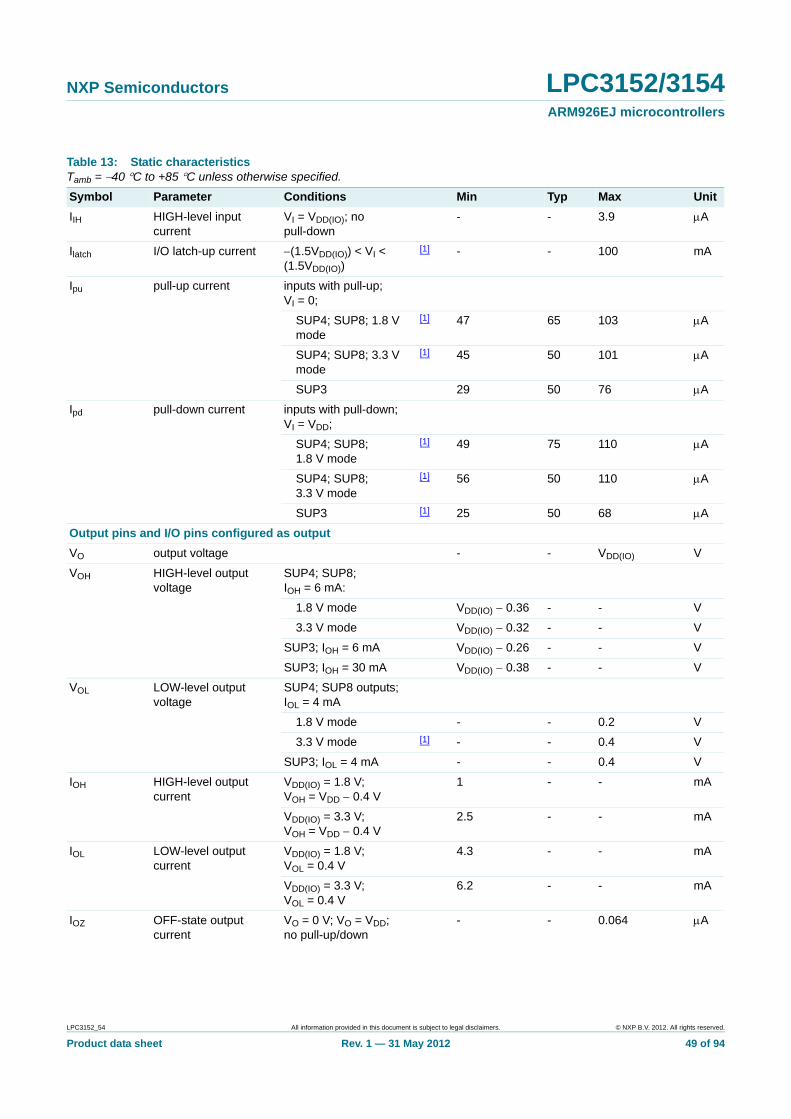
NXP Semiconductors LPC3152/3154ARM926EJ microcontrollers
IIH HIGH-level input current
VI = VDD(IO); no pull-down
- - 3.9 A
Ilatch I/O latch-up current (1.5VDD(IO)) < VI < (1.5VDD(IO))
[1] - - 100 mA
Ipu pull-up current inputs with pull-up; VI = 0;
SUP4; SUP8; 1.8 V mode
[1] 47 65 103 A
SUP4; SUP8; 3.3 V mode
[1] 45 50 101 A
SUP3 29 50 76 A
Ipd pull-down current inputs with pull-down;VI = VDD;
SUP4; SUP8; 1.8 V mode
[1] 49 75 110 A
SUP4; SUP8;3.3 V mode
[1] 56 50 110 A
SUP3 [1] 25 50 68 A
Output pins and I/O pins configured as output
VO output voltage - - VDD(IO) V
VOH HIGH-level output voltage
SUP4; SUP8;IOH = 6 mA:
1.8 V mode VDD(IO) 0.36 - - V
3.3 V mode VDD(IO) 0.32 - - V
SUP3; IOH = 6 mA VDD(IO) 0.26 - - V
SUP3; IOH = 30 mA VDD(IO) 0.38 - - V
VOL LOW-level output voltage
SUP4; SUP8 outputs; IOL = 4 mA
1.8 V mode - - 0.2 V
3.3 V mode [1] - - 0.4 V
SUP3; IOL = 4 mA - - 0.4 V
IOH HIGH-level output current
VDD(IO) = 1.8 V; VOH = VDD 0.4 V
1 - - mA
VDD(IO) = 3.3 V; VOH = VDD 0.4 V
2.5 - - mA
IOL LOW-level output current
VDD(IO) = 1.8 V; VOL = 0.4 V
4.3 - - mA
VDD(IO) = 3.3 V; VOL = 0.4 V
6.2 - - mA
IOZ OFF-state output current
VO = 0 V; VO = VDD;no pull-up/down
- - 0.064 A
Table 13: Static characteristicsTamb = 40 C to +85 C unless otherwise specified.
Symbol Parameter Conditions Min Typ Max Unit
LPC3152_54 All information provided in this document is subject to legal disclaimers. © NXP B.V. 2012. All rights reserved.
Product data sheet Rev. 1 — 31 May 2012 49 of 94
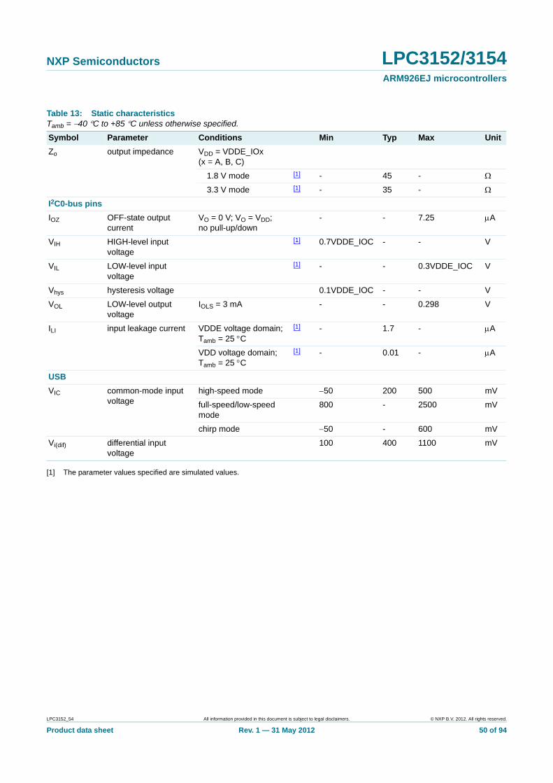
NXP Semiconductors LPC3152/3154ARM926EJ microcontrollers
[1] The parameter values specified are simulated values.
Zo output impedance VDD = VDDE_IOx (x = A, B, C)
1.8 V mode [1] - 45 -
3.3 V mode [1] - 35 -
I2C0-bus pins
IOZ OFF-state output current
VO = 0 V; VO = VDD;no pull-up/down
- - 7.25 A
VIH HIGH-level input voltage
[1] 0.7VDDE_IOC - - V
VIL LOW-level input voltage
[1] - - 0.3VDDE_IOC V
Vhys hysteresis voltage 0.1VDDE_IOC - - V
VOL LOW-level output voltage
IOLS = 3 mA - - 0.298 V
ILI input leakage current VDDE voltage domain; Tamb = 25 C
[1] - 1.7 - A
VDD voltage domain; Tamb = 25 C
[1] - 0.01 - A
USB
VIC common-mode input voltage
high-speed mode 50 200 500 mV
full-speed/low-speed mode
800 - 2500 mV
chirp mode 50 - 600 mV
Vi(dif) differential input voltage
100 400 1100 mV
Table 13: Static characteristicsTamb = 40 C to +85 C unless otherwise specified.
Symbol Parameter Conditions Min Typ Max Unit
LPC3152_54 All information provided in this document is subject to legal disclaimers. © NXP B.V. 2012. All rights reserved.
Product data sheet Rev. 1 — 31 May 2012 50 of 94
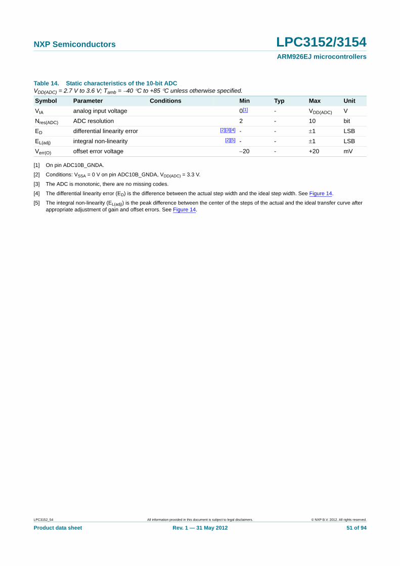
NXP Semiconductors LPC3152/3154ARM926EJ microcontrollers
[1] On pin ADC10B_GNDA.
[2] Conditions: VSSA = 0 V on pin ADC10B_GNDA, VDD(ADC) = 3.3 V.
[3] The ADC is monotonic, there are no missing codes.
[4] The differential linearity error (ED) is the difference between the actual step width and the ideal step width. See Figure 14.
[5] The integral non-linearity (EL(adj)) is the peak difference between the center of the steps of the actual and the ideal transfer curve after appropriate adjustment of gain and offset errors. See Figure 14.
Table 14. Static characteristics of the 10-bit ADCVDD(ADC) = 2.7 V to 3.6 V; Tamb = 40 C to +85 C unless otherwise specified.
Symbol Parameter Conditions Min Typ Max Unit
VIA analog input voltage 0[1] - VDD(ADC) V
Nres(ADC) ADC resolution 2 - 10 bit
ED differential linearity error [2][3][4] - - 1 LSB
EL(adj) integral non-linearity [2][5] - - 1 LSB
Verr(O) offset error voltage 20 - +20 mV
LPC3152_54 All information provided in this document is subject to legal disclaimers. © NXP B.V. 2012. All rights reserved.
Product data sheet Rev. 1 — 31 May 2012 51 of 94
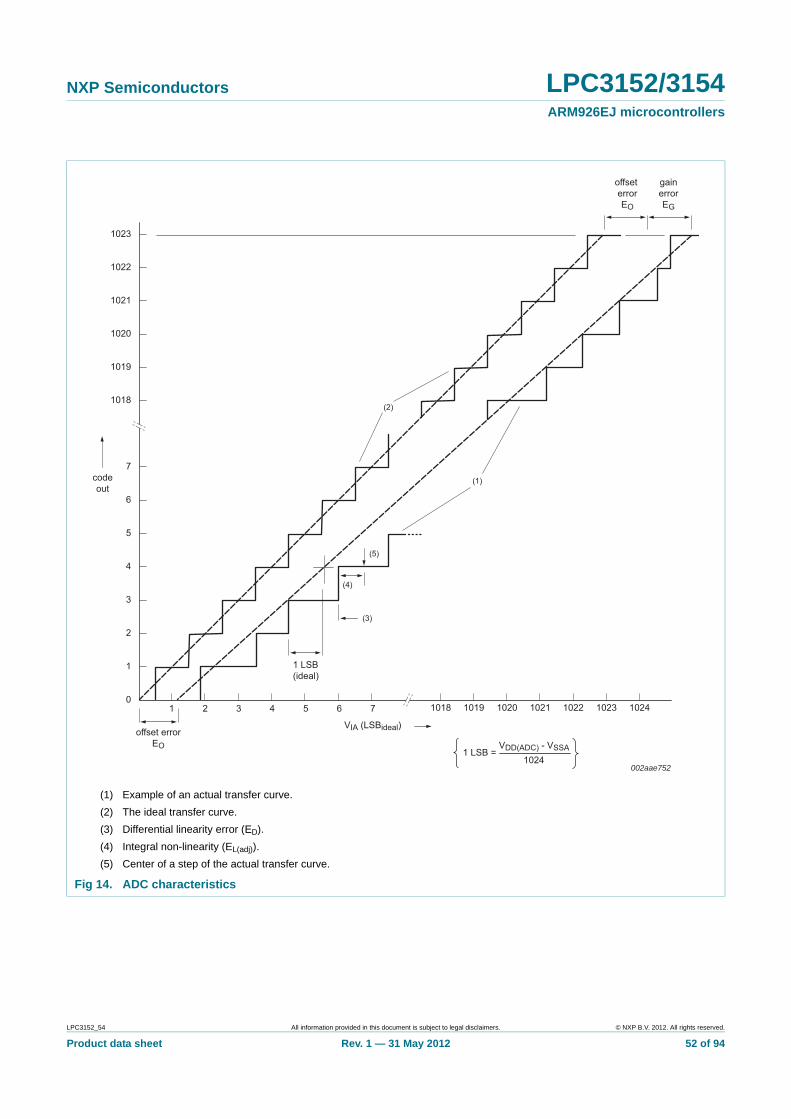
NXP Semiconductors LPC3152/3154ARM926EJ microcontrollers
(1) Example of an actual transfer curve.
(2) The ideal transfer curve.
(3) Differential linearity error (ED).
(4) Integral non-linearity (EL(adj)).
(5) Center of a step of the actual transfer curve.
Fig 14. ADC characteristics
002aae752
1023
1022
1021
1020
1019
(2)
(1)
10241018 1019 1020 1021 1022 102371 2 3 4 5 6
7
6
5
4
3
2
1
0
1018
(5)
(4)
(3)
1 LSB(ideal)
codeout
VDD(ADC) - VSSA 1024
offset errorEO
gainerrorEG
offset errorEO
VIA (LSBideal)
1 LSB =
LPC3152_54 All information provided in this document is subject to legal disclaimers. © NXP B.V. 2012. All rights reserved.
Product data sheet Rev. 1 — 31 May 2012 52 of 94
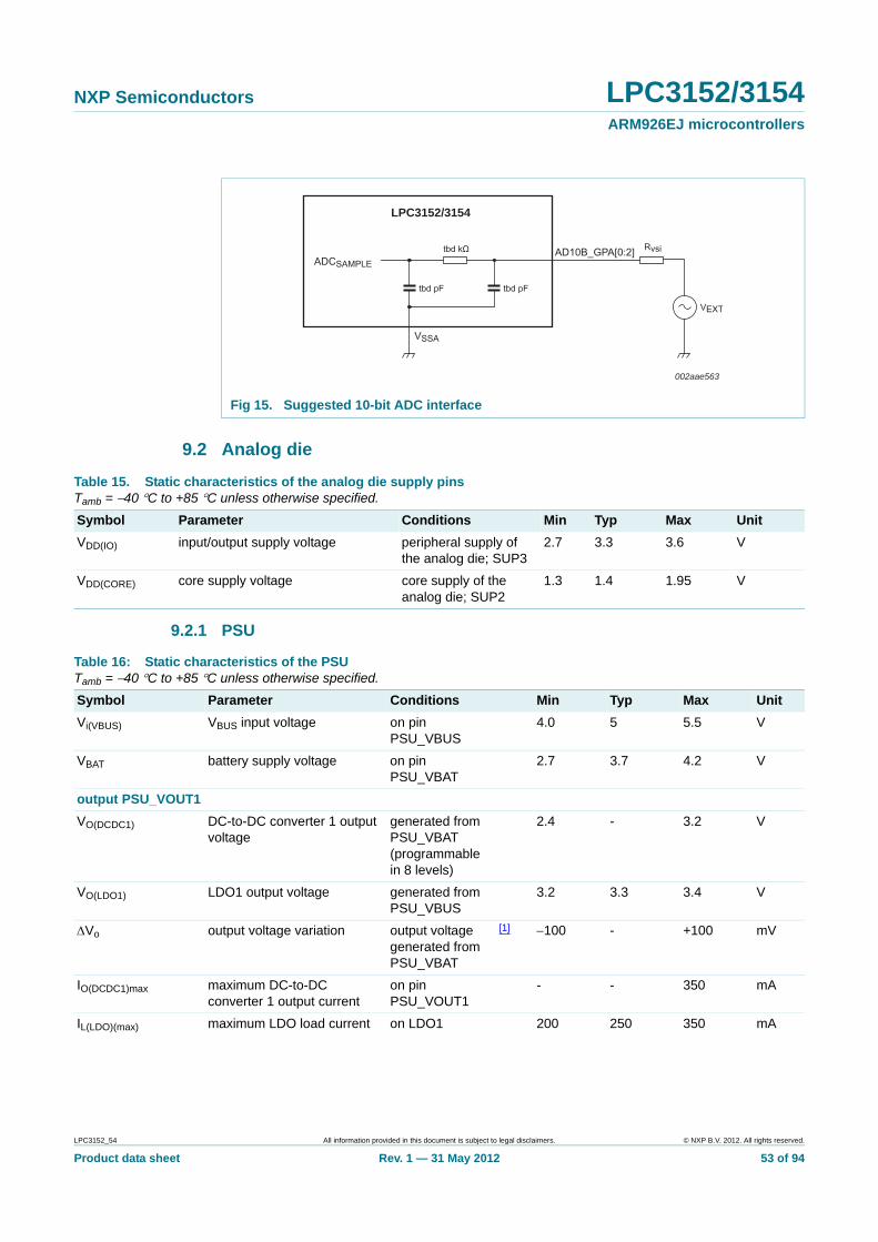
NXP Semiconductors LPC3152/3154ARM926EJ microcontrollers
9.2 Analog die
9.2.1 PSU
Fig 15. Suggested 10-bit ADC interface
LPC3152/3154
ADCSAMPLEAD10B_GPA[0:2]tbd kΩ
tbd pF tbd pF
Rvsi
VSSA
VEXT
002aae563
Table 15. Static characteristics of the analog die supply pinsTamb = 40 C to +85 C unless otherwise specified.
Symbol Parameter Conditions Min Typ Max Unit
VDD(IO) input/output supply voltage peripheral supply of the analog die; SUP3
2.7 3.3 3.6 V
VDD(CORE) core supply voltage core supply of the analog die; SUP2
1.3 1.4 1.95 V
Table 16: Static characteristics of the PSU Tamb = 40 C to +85 C unless otherwise specified.
Symbol Parameter Conditions Min Typ Max Unit
Vi(VBUS) VBUS input voltage on pin PSU_VBUS
4.0 5 5.5 V
VBAT battery supply voltage on pin PSU_VBAT
2.7 3.7 4.2 V
output PSU_VOUT1
VO(DCDC1) DC-to-DC converter 1 output voltage
generated from PSU_VBAT (programmable in 8 levels)
2.4 - 3.2 V
VO(LDO1) LDO1 output voltage generated from PSU_VBUS
3.2 3.3 3.4 V
Vo output voltage variation output voltage generated from PSU_VBAT
[1] 100 - +100 mV
IO(DCDC1)max maximum DC-to-DC converter 1 output current
on pin PSU_VOUT1
- - 350 mA
IL(LDO)(max) maximum LDO load current on LDO1 200 250 350 mA
LPC3152_54 All information provided in this document is subject to legal disclaimers. © NXP B.V. 2012. All rights reserved.
Product data sheet Rev. 1 — 31 May 2012 53 of 94
NXP Semiconductors LPC3152/3154ARM926EJ microcontrollers
[1] Deviation of output voltage on pin PSU_VOUTn from its nominal, programmed value.
output PSU_VOUT2
VO(DCDC2) DC-to-DC converter 2 output voltage
generated from PSU_VBAT (programmable in 8 levels)
0.9 - 1.4 V
VO(LDO2) LDO2 output voltage generated from PSU_VBUS (LDO1 on)
1.15 1.2 1.25 V
Vo output voltage variation output voltage generated from PSU_VBAT
[1] 50 - +50 mV
IO(DCDC2)max maximum DC-to-DC converter 2 output current
on pin PSU_VOUT2
- - 250 mA
IL(LDO)(max) maximum LDO load current on LDO2 80 - 120 mA
output PSU_VOUT3
VO output voltage generated from either PSU_VBAT or PSU_VBUS (programmable in 2 levels)
- 1.4 1.8 V
on LDO3 of VO = 1.4 V (default)
1.35 1.4 1.45 V
on LDO3 of VO = 1.8 V (default)
1.75 1.8 1.85 V
IL(LDO)(max) maximum LDO load current on pin PSU_VOUT3
- - 80 mA
DC-to-DC converter
DCDC DC-to-DC converter efficiency
- 85 - %
fclk clock frequency - 12 - MHz
fosc oscillator frequency 8 10 12 MHz
fsw switching frequency - 1 - MHz
Table 16: Static characteristics of the PSU …continuedTamb = 40 C to +85 C unless otherwise specified.
Symbol Parameter Conditions Min Typ Max Unit
LPC3152_54 All information provided in this document is subject to legal disclaimers. © NXP B.V. 2012. All rights reserved.
Product data sheet Rev. 1 — 31 May 2012 54 of 94
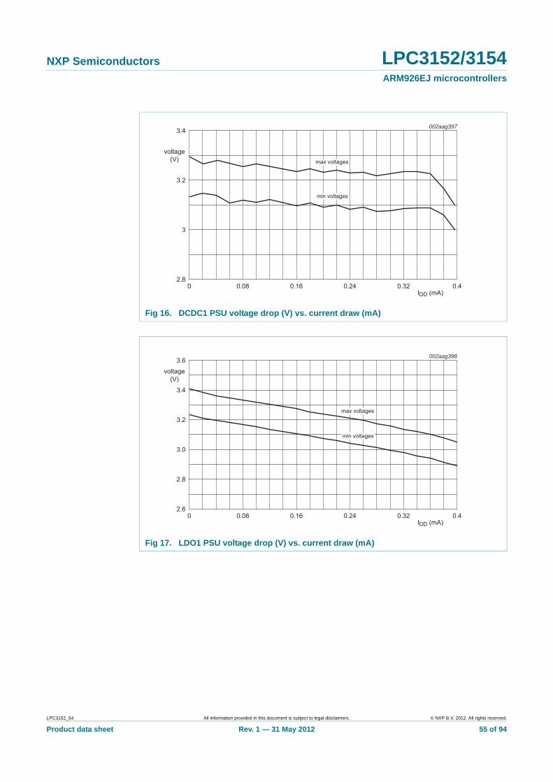
NXP Semiconductors LPC3152/3154ARM926EJ microcontrollers
Fig 16. DCDC1 PSU voltage drop (V) vs. current draw (mA)
Fig 17. LDO1 PSU voltage drop (V) vs. current draw (mA)
IDD (mA)0 0.32 0.40.240.08 0.16
002aag397
3
3.2
3.4
voltage(V)
2.8
max voltages
min voltages
IDD (mA)0 0.32 0.40.240.08 0.16
002aag398
3.0
3.2
2.8
3.4
3.6
voltage(V)
2.6
max voltages
min voltages
LPC3152_54 All information provided in this document is subject to legal disclaimers. © NXP B.V. 2012. All rights reserved.
Product data sheet Rev. 1 — 31 May 2012 55 of 94
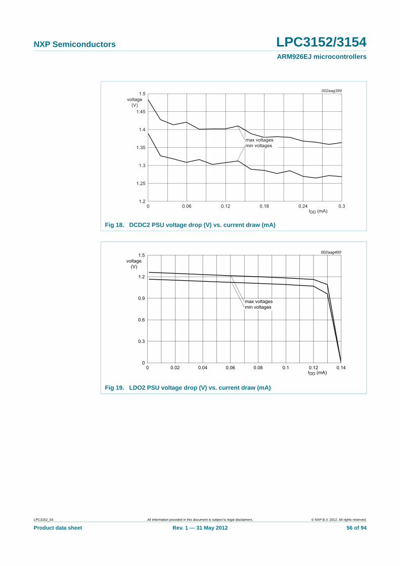
NXP Semiconductors LPC3152/3154ARM926EJ microcontrollers
Fig 18. DCDC2 PSU voltage drop (V) vs. current draw (mA)
Fig 19. LDO2 PSU voltage drop (V) vs. current draw (mA)
002aag399
0 0.06 0.12 0.18 0.24 0.31.2
1.25
1.3
1.35
1.4
1.45
1.5
IDD (mA)
voltage(V)
max voltagesmin voltages
002aag400
0 0.02 0.04 0.06 0.08 0.1 0.12 0.140
0.3
0.6
0.9
1.2
1.5
IDD (mA)
voltage(V)
max voltagesmin voltages
LPC3152_54 All information provided in this document is subject to legal disclaimers. © NXP B.V. 2012. All rights reserved.
Product data sheet Rev. 1 — 31 May 2012 56 of 94
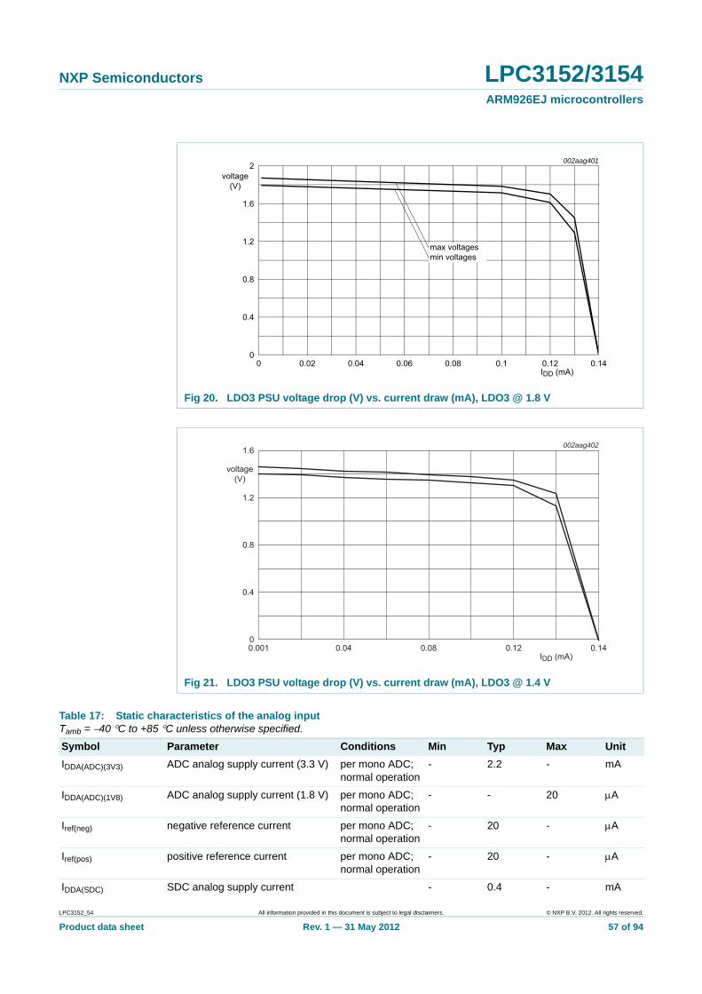
NXP Semiconductors LPC3152/3154ARM926EJ microcontrollers
Fig 20. LDO3 PSU voltage drop (V) vs. current draw (mA), LDO3 @ 1.8 V
Fig 21. LDO3 PSU voltage drop (V) vs. current draw (mA), LDO3 @ 1.4 V
002aag401
0 0.02 0.04 0.06 0.08 0.1 0.12 0.140
0.4
0.8
1.2
1.6
2
IDD (mA)
voltage(V)
max voltagesmin voltages
IDD (mA)0.001 0.140.120.080.04
002aag402
0.8
0.4
1.2
1.6
voltage(V)
0
Table 17: Static characteristics of the analog input Tamb = 40 C to +85 C unless otherwise specified.
Symbol Parameter Conditions Min Typ Max Unit
IDDA(ADC)(3V3) ADC analog supply current (3.3 V) per mono ADC; normal operation
- 2.2 - mA
IDDA(ADC)(1V8) ADC analog supply current (1.8 V) per mono ADC; normal operation
- - 20 A
Iref(neg) negative reference current per mono ADC; normal operation
- 20 - A
Iref(pos) positive reference current per mono ADC; normal operation
- 20 - A
IDDA(SDC) SDC analog supply current - 0.4 - mA
LPC3152_54 All information provided in this document is subject to legal disclaimers. © NXP B.V. 2012. All rights reserved.
Product data sheet Rev. 1 — 31 May 2012 57 of 94
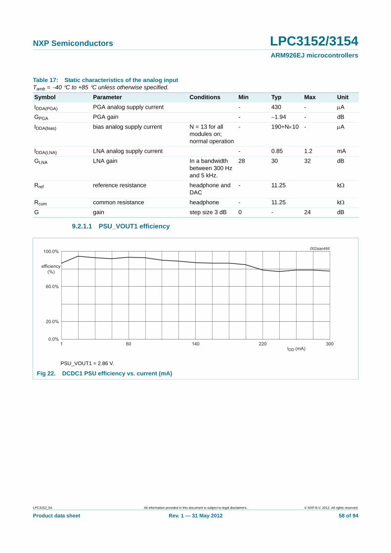
NXP Semiconductors LPC3152/3154ARM926EJ microcontrollers
9.2.1.1 PSU_VOUT1 efficiency
IDDA(PGA) PGA analog supply current - 430 - A
GPGA PGA gain - 1.94 - dB
IDDA(bias) bias analog supply current N = 13 for all modules on; normal operation
- 190+N10 - A
IDDA(LNA) LNA analog supply current - 0.85 1.2 mA
GLNA LNA gain In a bandwidth between 300 Hz and 5 kHz.
28 30 32 dB
Rref reference resistance headphone and DAC
- 11.25 k
Rcom common resistance headphone - 11.25 k
G gain step size 3 dB 0 - 24 dB
Table 17: Static characteristics of the analog input Tamb = 40 C to +85 C unless otherwise specified.
Symbol Parameter Conditions Min Typ Max Unit
PSU_VOUT1 = 2.86 V.
Fig 22. DCDC1 PSU efficiency vs. current (mA)
002aae466
IDD (mA)1 30022060 140
20.0%
60.0%
100.0%
efficiency(%)
0.0%
LPC3152_54 All information provided in this document is subject to legal disclaimers. © NXP B.V. 2012. All rights reserved.
Product data sheet Rev. 1 — 31 May 2012 58 of 94
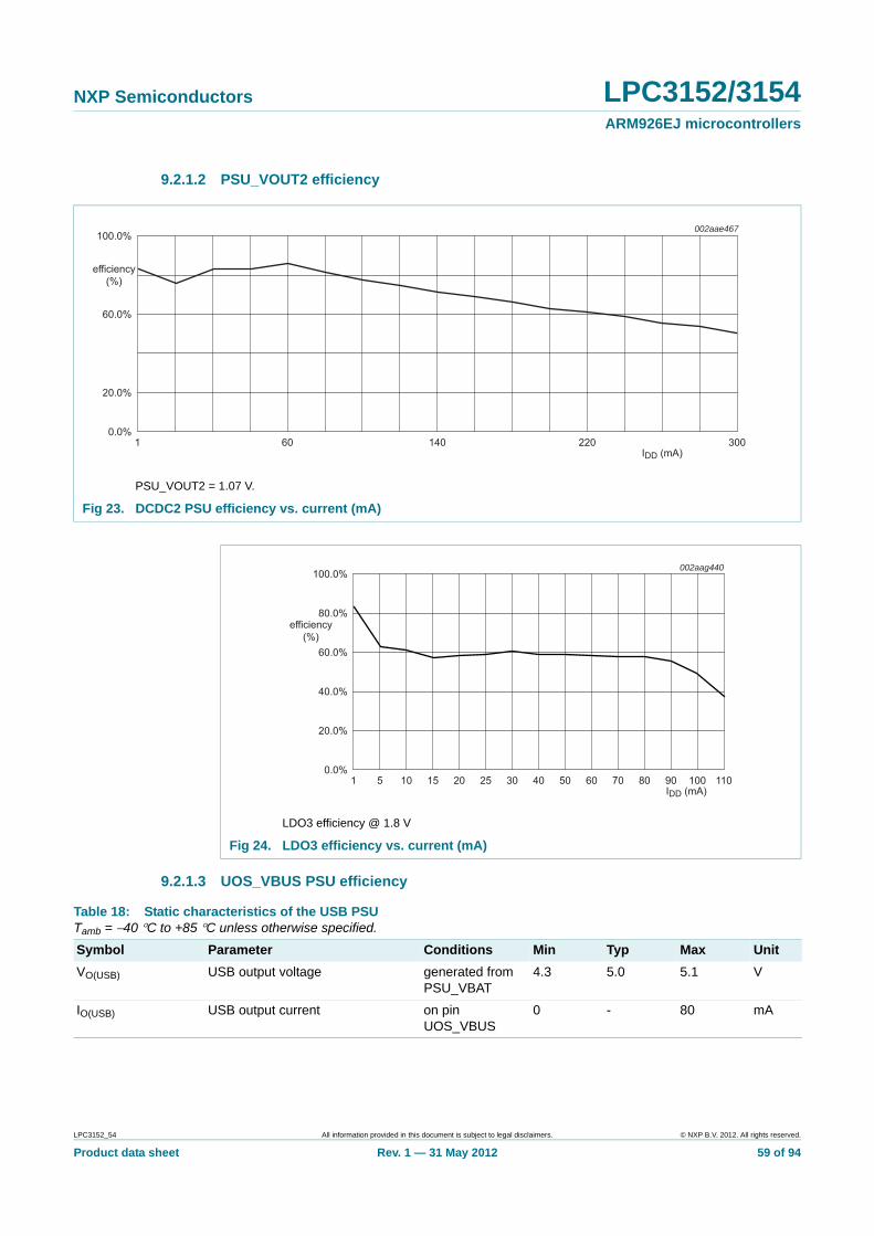
NXP Semiconductors LPC3152/3154ARM926EJ microcontrollers
9.2.1.2 PSU_VOUT2 efficiency
9.2.1.3 UOS_VBUS PSU efficiency
PSU_VOUT2 = 1.07 V.
Fig 23. DCDC2 PSU efficiency vs. current (mA)
002aae467
IDD (mA)1 30022060 140
20.0%
60.0%
100.0%
efficiency(%)
0.0%
LDO3 efficiency @ 1.8 V
Fig 24. LDO3 efficiency vs. current (mA)
IDD (mA)1 5 10 15 20 25 30 40 11090 10050 60 70 80
002aag440
20.0%
40.0%
60.0%
80.0%
100.0%
efficiency(%)
0.0%
Table 18: Static characteristics of the USB PSUTamb = 40 C to +85 C unless otherwise specified.
Symbol Parameter Conditions Min Typ Max Unit
VO(USB) USB output voltage generated from PSU_VBAT
4.3 5.0 5.1 V
IO(USB) USB output current on pin UOS_VBUS
0 - 80 mA
LPC3152_54 All information provided in this document is subject to legal disclaimers. © NXP B.V. 2012. All rights reserved.
Product data sheet Rev. 1 — 31 May 2012 59 of 94
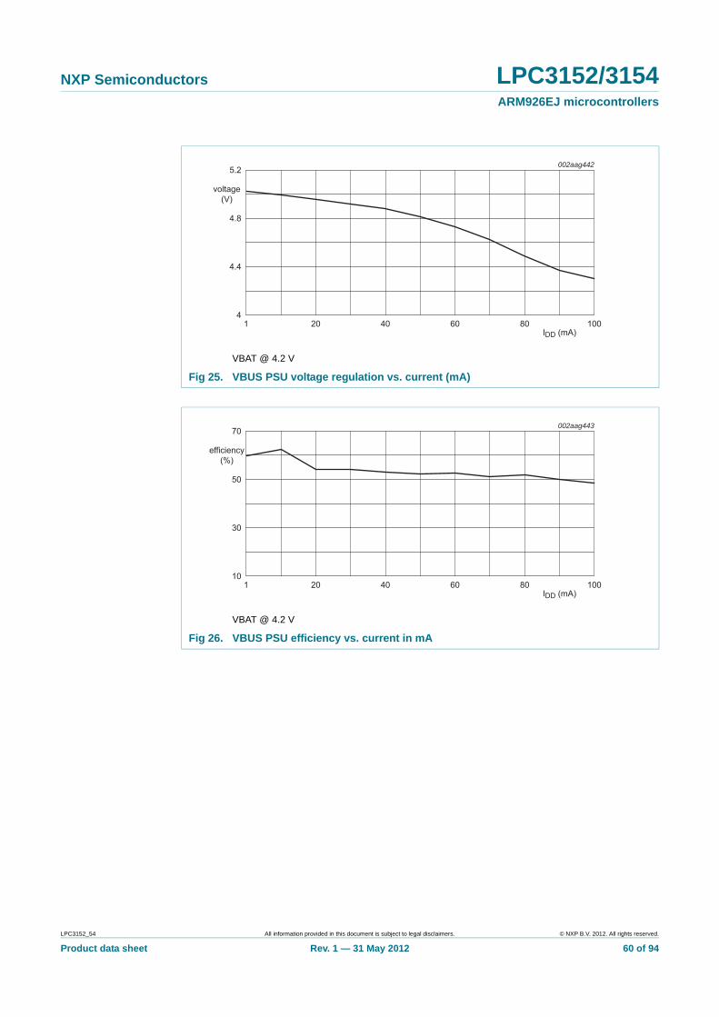
NXP Semiconductors LPC3152/3154ARM926EJ microcontrollers
VBAT @ 4.2 V
Fig 25. VBUS PSU voltage regulation vs. current (mA)
VBAT @ 4.2 V
Fig 26. VBUS PSU efficiency vs. current in mA
IDD (mA)1 1008040 6020
002aag442
4.4
4
4.8
5.2
voltage(V)
IDD (mA)1 1008040 6020
002aag443
30
10
50
70
efficiency(%)
LPC3152_54 All information provided in this document is subject to legal disclaimers. © NXP B.V. 2012. All rights reserved.
Product data sheet Rev. 1 — 31 May 2012 60 of 94
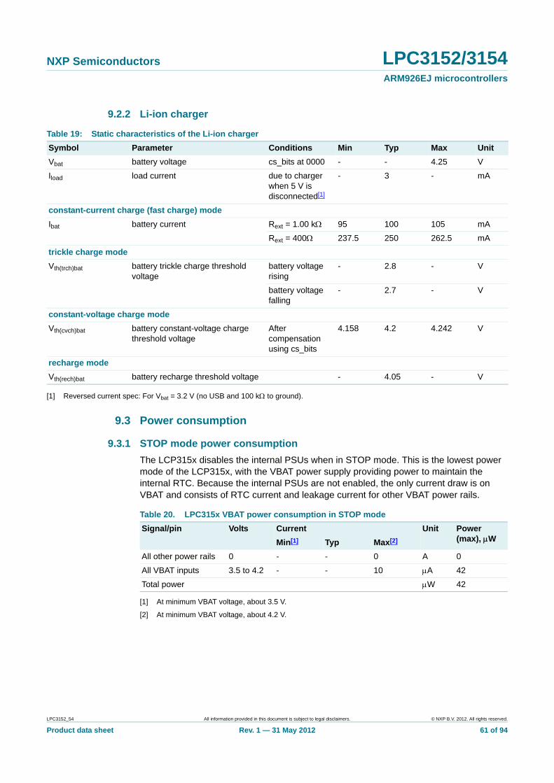
NXP Semiconductors LPC3152/3154ARM926EJ microcontrollers
9.2.2 Li-ion charger
[1] Reversed current spec: For Vbat = 3.2 V (no USB and 100 k to ground).
9.3 Power consumption
9.3.1 STOP mode power consumption
The LCP315x disables the internal PSUs when in STOP mode. This is the lowest power mode of the LCP315x, with the VBAT power supply providing power to maintain the internal RTC. Because the internal PSUs are not enabled, the only current draw is on VBAT and consists of RTC current and leakage current for other VBAT power rails.
[1] At minimum VBAT voltage, about 3.5 V.
[2] At minimum VBAT voltage, about 4.2 V.
Table 19: Static characteristics of the Li-ion charger
Symbol Parameter Conditions Min Typ Max Unit
Vbat battery voltage cs_bits at 0000 - - 4.25 V
Iload load current due to charger when 5 V is disconnected[1]
- 3 - mA
constant-current charge (fast charge) mode
Ibat battery current Rext = 1.00 k 95 100 105 mA
Rext = 400 237.5 250 262.5 mA
trickle charge mode
Vth(trch)bat battery trickle charge threshold voltage
battery voltage rising
- 2.8 - V
battery voltage falling
- 2.7 - V
constant-voltage charge mode
Vth(cvch)bat battery constant-voltage charge threshold voltage
After compensation using cs_bits
4.158 4.2 4.242 V
recharge mode
Vth(rech)bat battery recharge threshold voltage - 4.05 - V
Table 20. LPC315x VBAT power consumption in STOP mode
Signal/pin Volts Current Unit Power (max), WMin[1] Typ Max[2]
All other power rails 0 - - 0 A 0
All VBAT inputs 3.5 to 4.2 - - 10 A 42
Total power W 42
LPC3152_54 All information provided in this document is subject to legal disclaimers. © NXP B.V. 2012. All rights reserved.
Product data sheet Rev. 1 — 31 May 2012 61 of 94
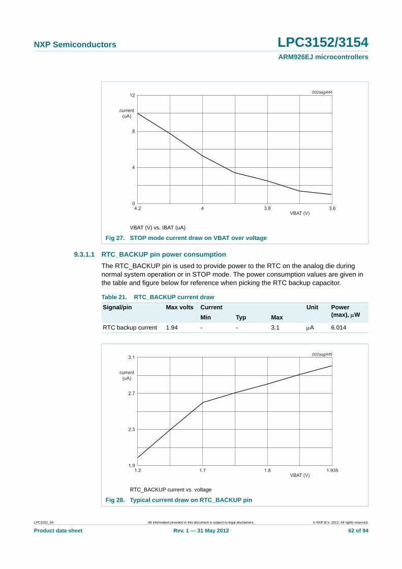
NXP Semiconductors LPC3152/3154ARM926EJ microcontrollers
9.3.1.1 RTC_BACKUP pin power consumption
The RTC_BACKUP pin is used to provide power to the RTC on the analog die during normal system operation or in STOP mode. The power consumption values are given in the table and figure below for reference when picking the RTC backup capacitor.
VBAT (V) vs. IBAT (uA)
Fig 27. STOP mode current draw on VBAT over voltage
VBAT (V)4.2 3.63.84
002aag444
4
8
12
current(uA)
0
Table 21. RTC_BACKUP current draw
Signal/pin Max volts Current Unit Power (max), WMin Typ Max
RTC backup current 1.94 - - 3.1 A 6.014
RTC_BACKUP current vs. voltage
Fig 28. Typical current draw on RTC_BACKUP pin
VBAT (V)1.2 1.9351.81.7
002aag445
2.3
2.7
3.1
current(uA)
1.9
LPC3152_54 All information provided in this document is subject to legal disclaimers. © NXP B.V. 2012. All rights reserved.
Product data sheet Rev. 1 — 31 May 2012 62 of 94
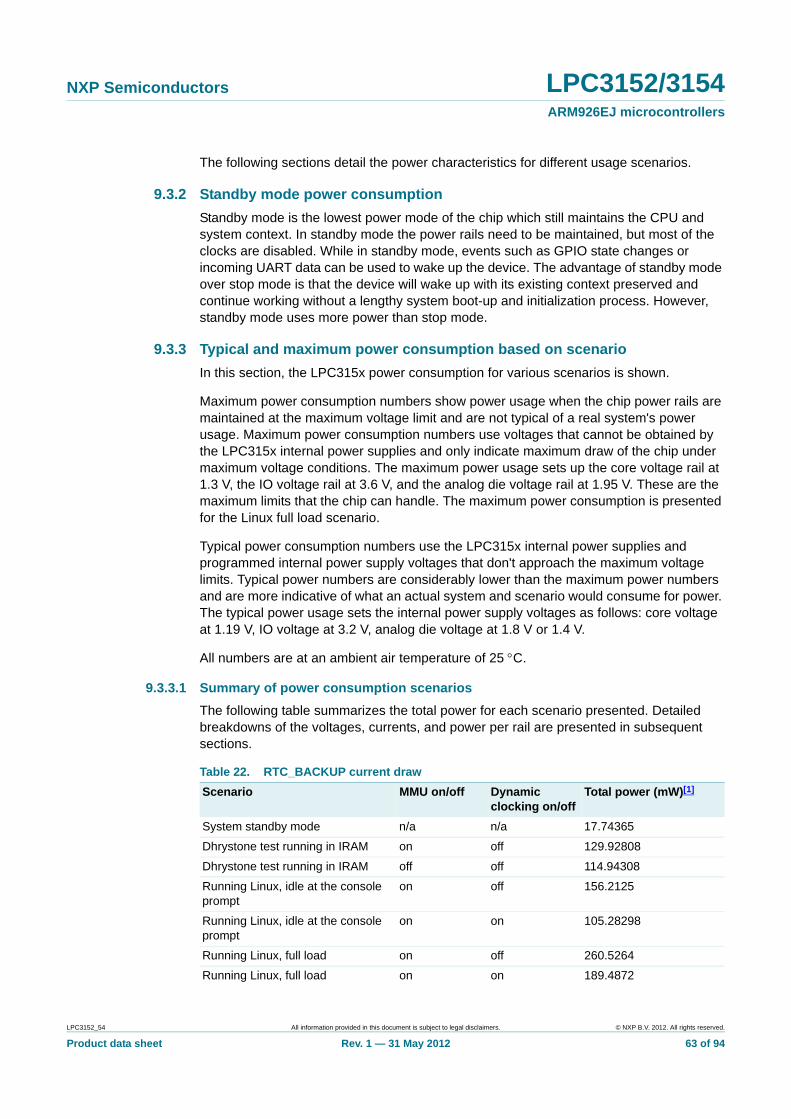
NXP Semiconductors LPC3152/3154ARM926EJ microcontrollers
The following sections detail the power characteristics for different usage scenarios.
9.3.2 Standby mode power consumption
Standby mode is the lowest power mode of the chip which still maintains the CPU and system context. In standby mode the power rails need to be maintained, but most of the clocks are disabled. While in standby mode, events such as GPIO state changes or incoming UART data can be used to wake up the device. The advantage of standby mode over stop mode is that the device will wake up with its existing context preserved and continue working without a lengthy system boot-up and initialization process. However, standby mode uses more power than stop mode.
9.3.3 Typical and maximum power consumption based on scenario
In this section, the LPC315x power consumption for various scenarios is shown.
Maximum power consumption numbers show power usage when the chip power rails are maintained at the maximum voltage limit and are not typical of a real system's power usage. Maximum power consumption numbers use voltages that cannot be obtained by the LPC315x internal power supplies and only indicate maximum draw of the chip under maximum voltage conditions. The maximum power usage sets up the core voltage rail at 1.3 V, the IO voltage rail at 3.6 V, and the analog die voltage rail at 1.95 V. These are the maximum limits that the chip can handle. The maximum power consumption is presented for the Linux full load scenario.
Typical power consumption numbers use the LPC315x internal power supplies and programmed internal power supply voltages that don't approach the maximum voltage limits. Typical power numbers are considerably lower than the maximum power numbers and are more indicative of what an actual system and scenario would consume for power. The typical power usage sets the internal power supply voltages as follows: core voltage at 1.19 V, IO voltage at 3.2 V, analog die voltage at 1.8 V or 1.4 V.
All numbers are at an ambient air temperature of 25 C.
9.3.3.1 Summary of power consumption scenarios
The following table summarizes the total power for each scenario presented. Detailed breakdowns of the voltages, currents, and power per rail are presented in subsequent sections.
Table 22. RTC_BACKUP current draw
Scenario MMU on/off Dynamic clocking on/off
Total power (mW)[1]
System standby mode n/a n/a 17.74365
Dhrystone test running in IRAM on off 129.92808
Dhrystone test running in IRAM off off 114.94308
Running Linux, idle at the console prompt
on off 156.2125
Running Linux, idle at the console prompt
on on 105.28298
Running Linux, full load on off 260.5264
Running Linux, full load on on 189.4872
LPC3152_54 All information provided in this document is subject to legal disclaimers. © NXP B.V. 2012. All rights reserved.
Product data sheet Rev. 1 — 31 May 2012 63 of 94
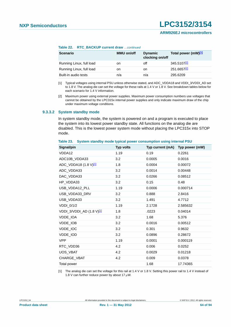
NXP Semiconductors LPC3152/3154ARM926EJ microcontrollers
[1] Typical voltages using internal PSU unless otherwise stated, and ADC_VDDA18 and VDDI_3/VDDI_AD set to 1.8 V. The analog die can set the voltage for these rails at 1.4 V or 1.8 V. See breakdown tables below for each scenario for 1.4 V information.
[2] Maximum power using external power supplies. Maximum power consumption numbers use voltages that cannot be obtained by the LPC315x internal power supplies and only indicate maximum draw of the chip under maximum voltage conditions.
9.3.3.2 System standby mode
In system standby mode, the system is powered on and a program is executed to place the system into its lowest power standby state. All functions on the analog die are disabled. This is the lowest power system mode without placing the LPC315x into STOP mode.
[1] The analog die can set the voltage for this rail at 1.4 V or 1.8 V. Setting this power rail to 1.4 V instead of 1.8 V can further reduce power by about 17 W.
Running Linux, full load on off 345.5107[2]
Running Linux, full load on on 251.6657[2]
Built-in audio tests n/a n/a 295.6209
Table 22. RTC_BACKUP current draw …continued
Scenario MMU on/off Dynamic clocking on/off
Total power (mW)[1]
Table 23. System standby mode typical power consumption using internal PSU
Signal/pin Typ volts Typ current (mA) Typ power (mW)
VDDA12 1.19 0.19 0.2261
ADC10B_VDDA33 3.2 0.0005 0.0016
ADC_VDDA18 (1.8 V)[1] 1.8 0.0004 0.00072
ADC_VDDA33 3.2 0.0014 0.00448
DAC_VDDA33 3.2 0.0266 0.08512
HP_VDDA33 3.2 0.15 0.48
USB_VDDA12_PLL 1.19 0.0006 0.000714
USB_VDDA33_DRV 3.2 0.888 2.8416
USB_VDDA33 3.2 1.491 4.7712
VDDI_0/1/2 1.19 2.1728 2.585632
VDDI_3/VDDI_AD (1.8 V)[1] 1.8 .0223 0.04014
VDDE_IOA 3.2 1.68 5.376
VDDE_IOB 3.2 0.0016 0.00512
VDDE_IOC 3.2 0.301 0.9632
VDDE_IOD 3.2 0.0896 0.28672
VPP 1.19 0.0001 0.000119
RTC_VDD36 4.2 0.006 0.0252
UOS_VBAT 4.2 0.0029 0.01218
CHARGE_VBAT 4.2 0.009 0.0378
Total power 1.68 17.74365
LPC3152_54 All information provided in this document is subject to legal disclaimers. © NXP B.V. 2012. All rights reserved.
Product data sheet Rev. 1 — 31 May 2012 64 of 94
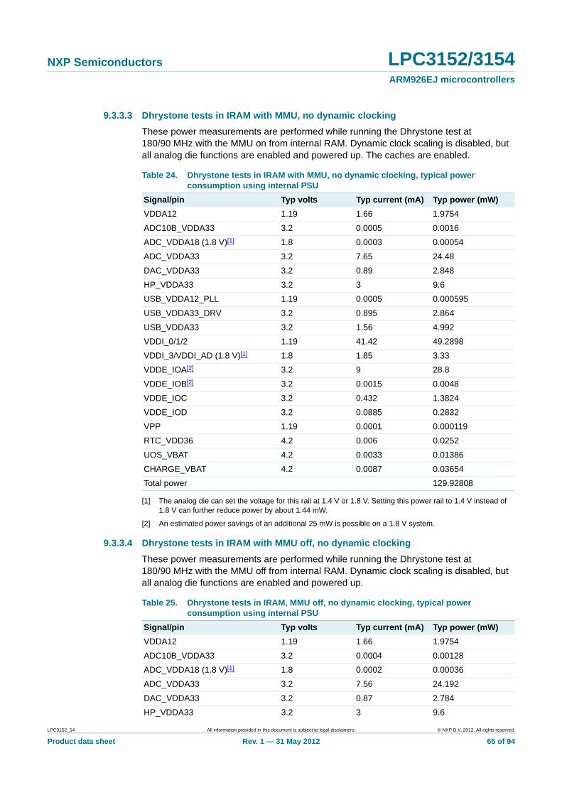
NXP Semiconductors LPC3152/3154ARM926EJ microcontrollers
9.3.3.3 Dhrystone tests in IRAM with MMU, no dynamic clocking
These power measurements are performed while running the Dhrystone test at 180/90 MHz with the MMU on from internal RAM. Dynamic clock scaling is disabled, but all analog die functions are enabled and powered up. The caches are enabled.
[1] The analog die can set the voltage for this rail at 1.4 V or 1.8 V. Setting this power rail to 1.4 V instead of 1.8 V can further reduce power by about 1.44 mW.
[2] An estimated power savings of an additional 25 mW is possible on a 1.8 V system.
9.3.3.4 Dhrystone tests in IRAM with MMU off, no dynamic clocking
These power measurements are performed while running the Dhrystone test at 180/90 MHz with the MMU off from internal RAM. Dynamic clock scaling is disabled, but all analog die functions are enabled and powered up.
Table 24. Dhrystone tests in IRAM with MMU, no dynamic clocking, typical power consumption using internal PSU
Signal/pin Typ volts Typ current (mA) Typ power (mW)
VDDA12 1.19 1.66 1.9754
ADC10B_VDDA33 3.2 0.0005 0.0016
ADC_VDDA18 (1.8 V)[1] 1.8 0.0003 0.00054
ADC_VDDA33 3.2 7.65 24.48
DAC_VDDA33 3.2 0.89 2.848
HP_VDDA33 3.2 3 9.6
USB_VDDA12_PLL 1.19 0.0005 0.000595
USB_VDDA33_DRV 3.2 0.895 2.864
USB_VDDA33 3.2 1.56 4.992
VDDI_0/1/2 1.19 41.42 49.2898
VDDI_3/VDDI_AD (1.8 V)[1] 1.8 1.85 3.33
VDDE_IOA[2] 3.2 9 28.8
VDDE_IOB[2] 3.2 0.0015 0.0048
VDDE_IOC 3.2 0.432 1.3824
VDDE_IOD 3.2 0.0885 0.2832
VPP 1.19 0.0001 0.000119
RTC_VDD36 4.2 0.006 0.0252
UOS_VBAT 4.2 0.0033 0.01386
CHARGE_VBAT 4.2 0.0087 0.03654
Total power 129.92808
Table 25. Dhrystone tests in IRAM, MMU off, no dynamic clocking, typical power consumption using internal PSU
Signal/pin Typ volts Typ current (mA) Typ power (mW)
VDDA12 1.19 1.66 1.9754
ADC10B_VDDA33 3.2 0.0004 0.00128
ADC_VDDA18 (1.8 V)[1] 1.8 0.0002 0.00036
ADC_VDDA33 3.2 7.56 24.192
DAC_VDDA33 3.2 0.87 2.784
HP_VDDA33 3.2 3 9.6
LPC3152_54 All information provided in this document is subject to legal disclaimers. © NXP B.V. 2012. All rights reserved.
Product data sheet Rev. 1 — 31 May 2012 65 of 94
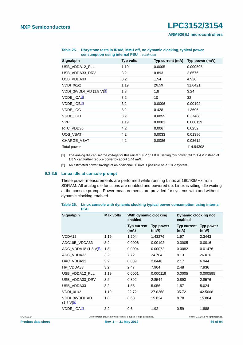
NXP Semiconductors LPC3152/3154ARM926EJ microcontrollers
[1] The analog die can set the voltage for this rail at 1.4 V or 1.8 V. Setting this power rail to 1.4 V instead of 1.8 V can further reduce power by about 1.44 mW.
[2] An estimated power savings of an additional 30 mW is possible on a 1.8 V system.
9.3.3.5 Linux idle at console prompt
These power measurements are performed while running Linux at 180/90MHz from SDRAM. All analog die functions are enabled and powered up. Linux is sitting idle waiting at the console prompt. Power measurements are provided for systems with and without dynamic clocking enabled.
USB_VDDA12_PLL 1.19 0.0005 0.000595
USB_VDDA33_DRV 3.2 0.893 2.8576
USB_VDDA33 3.2 1.54 4.928
VDDI_0/1/2 1.19 26.59 31.6421
VDDI_3/VDDI_AD (1.8 V)[1] 1.8 1.8 3.24
VDDE_IOA[2] 3.2 10 32
VDDE_IOB[2] 3.2 0.0006 0.00192
VDDE_IOC 3.2 0.428 1.3696
VDDE_IOD 3.2 0.0859 0.27488
VPP 1.19 0.0001 0.000119
RTC_VDD36 4.2 0.006 0.0252
UOS_VBAT 4.2 0.0033 0.01386
CHARGE_VBAT 4.2 0.0086 0.03612
Total power 114.94308
Table 25. Dhrystone tests in IRAM, MMU off, no dynamic clocking, typical power consumption using internal PSU …continued
Signal/pin Typ volts Typ current (mA) Typ power (mW)
Table 26. Linux console with dynamic clocking typical power consumption using internal PSU
Signal/pin Max volts With dynamic clocking enabled
Dynamic clocking not enabled
Typ current (mA)
Typ power (mW)
Typ current (mA)
Typ power (mW)
VDDA12 1.19 1.204 1.43276 1.97 2.3443
ADC10B_VDDA33 3.2 0.0006 0.00192 0.0005 0.0016
ADC_VDDA18 (1.8 V)[1] 1.8 0.0004 0.00072 0.0082 0.01476
ADC_VDDA33 3.2 7.72 24.704 8.13 26.016
DAC_VDDA33 3.2 0.889 2.8448 2.17 6.944
HP_VDDA33 3.2 2.47 7.904 2.48 7.936
USB_VDDA12_PLL 1.19 0.0001 0.000119 0.0005 0.000595
USB_VDDA33_DRV 3.2 0.892 2.8544 0.893 2.8576
USB_VDDA33 3.2 1.58 5.056 1.57 5.024
VDDI_0/1/2 1.19 22.72 27.0368 35.72 42.5068
VDDI_3/VDDI_AD (1.8 V)[1]
1.8 8.68 15.624 8.78 15.804
VDDE_IOA[2] 3.2 0.6 1.92 0.59 1.888
LPC3152_54 All information provided in this document is subject to legal disclaimers. © NXP B.V. 2012. All rights reserved.
Product data sheet Rev. 1 — 31 May 2012 66 of 94
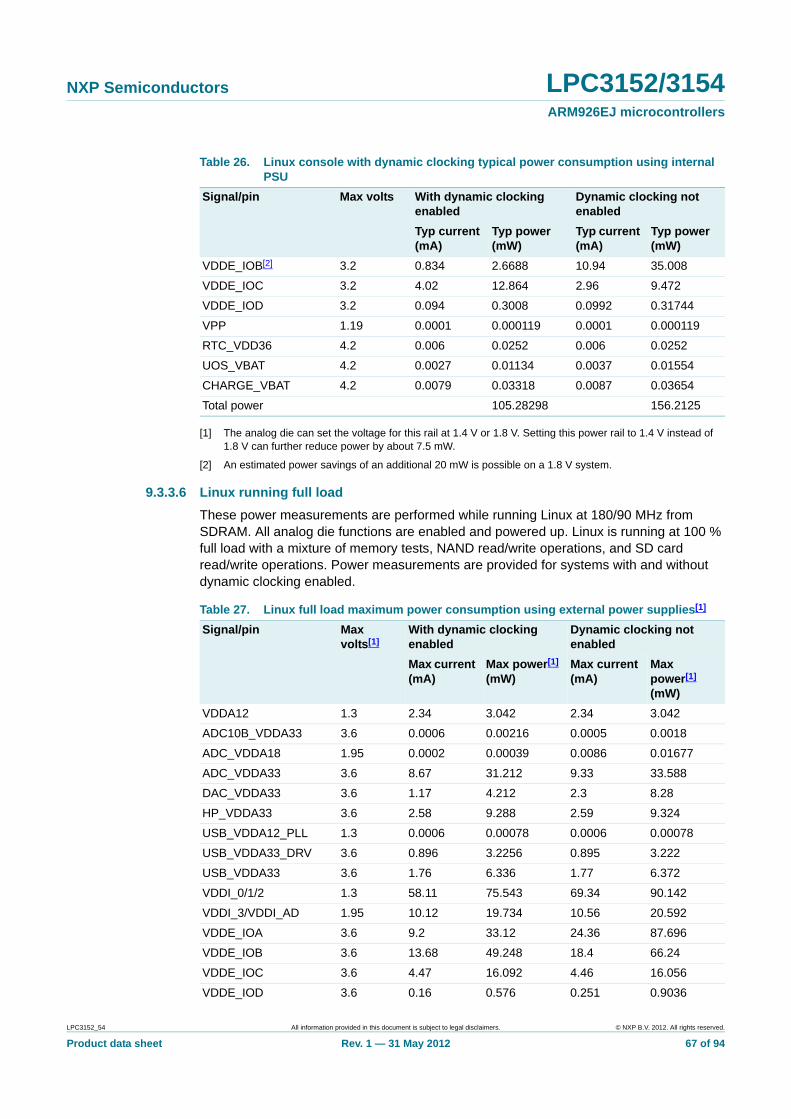
NXP Semiconductors LPC3152/3154ARM926EJ microcontrollers
[1] The analog die can set the voltage for this rail at 1.4 V or 1.8 V. Setting this power rail to 1.4 V instead of 1.8 V can further reduce power by about 7.5 mW.
[2] An estimated power savings of an additional 20 mW is possible on a 1.8 V system.
9.3.3.6 Linux running full load
These power measurements are performed while running Linux at 180/90 MHz from SDRAM. All analog die functions are enabled and powered up. Linux is running at 100 % full load with a mixture of memory tests, NAND read/write operations, and SD card read/write operations. Power measurements are provided for systems with and without dynamic clocking enabled.
VDDE_IOB[2] 3.2 0.834 2.6688 10.94 35.008
VDDE_IOC 3.2 4.02 12.864 2.96 9.472
VDDE_IOD 3.2 0.094 0.3008 0.0992 0.31744
VPP 1.19 0.0001 0.000119 0.0001 0.000119
RTC_VDD36 4.2 0.006 0.0252 0.006 0.0252
UOS_VBAT 4.2 0.0027 0.01134 0.0037 0.01554
CHARGE_VBAT 4.2 0.0079 0.03318 0.0087 0.03654
Total power 105.28298 156.2125
Table 26. Linux console with dynamic clocking typical power consumption using internal PSU
Signal/pin Max volts With dynamic clocking enabled
Dynamic clocking not enabled
Typ current (mA)
Typ power (mW)
Typ current (mA)
Typ power (mW)
Table 27. Linux full load maximum power consumption using external power supplies[1]
Signal/pin Max volts[1]
With dynamic clocking enabled
Dynamic clocking not enabled
Max current (mA)
Max power[1] (mW)
Max current (mA)
Max power[1] (mW)
VDDA12 1.3 2.34 3.042 2.34 3.042
ADC10B_VDDA33 3.6 0.0006 0.00216 0.0005 0.0018
ADC_VDDA18 1.95 0.0002 0.00039 0.0086 0.01677
ADC_VDDA33 3.6 8.67 31.212 9.33 33.588
DAC_VDDA33 3.6 1.17 4.212 2.3 8.28
HP_VDDA33 3.6 2.58 9.288 2.59 9.324
USB_VDDA12_PLL 1.3 0.0006 0.00078 0.0006 0.00078
USB_VDDA33_DRV 3.6 0.896 3.2256 0.895 3.222
USB_VDDA33 3.6 1.76 6.336 1.77 6.372
VDDI_0/1/2 1.3 58.11 75.543 69.34 90.142
VDDI_3/VDDI_AD 1.95 10.12 19.734 10.56 20.592
VDDE_IOA 3.6 9.2 33.12 24.36 87.696
VDDE_IOB 3.6 13.68 49.248 18.4 66.24
VDDE_IOC 3.6 4.47 16.092 4.46 16.056
VDDE_IOD 3.6 0.16 0.576 0.251 0.9036
LPC3152_54 All information provided in this document is subject to legal disclaimers. © NXP B.V. 2012. All rights reserved.
Product data sheet Rev. 1 — 31 May 2012 67 of 94
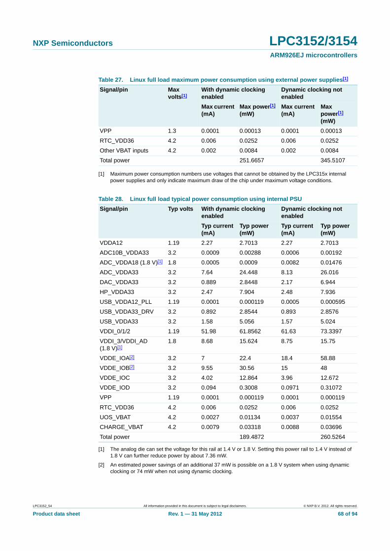
NXP Semiconductors LPC3152/3154ARM926EJ microcontrollers
[1] Maximum power consumption numbers use voltages that cannot be obtained by the LPC315x internal power supplies and only indicate maximum draw of the chip under maximum voltage conditions.
[1] The analog die can set the voltage for this rail at 1.4 V or 1.8 V. Setting this power rail to 1.4 V instead of 1.8 V can further reduce power by about 7.36 mW.
[2] An estimated power savings of an additional 37 mW is possible on a 1.8 V system when using dynamic clocking or 74 mW when not using dynamic clocking.
VPP 1.3 0.0001 0.00013 0.0001 0.00013
RTC_VDD36 4.2 0.006 0.0252 0.006 0.0252
Other VBAT inputs 4.2 0.002 0.0084 0.002 0.0084
Total power 251.6657 345.5107
Table 28. Linux full load typical power consumption using internal PSU
Signal/pin Typ volts With dynamic clocking enabled
Dynamic clocking not enabled
Typ current (mA)
Typ power (mW)
Typ current (mA)
Typ power (mW)
VDDA12 1.19 2.27 2.7013 2.27 2.7013
ADC10B_VDDA33 3.2 0.0009 0.00288 0.0006 0.00192
ADC_VDDA18 (1.8 V)[1] 1.8 0.0005 0.0009 0.0082 0.01476
ADC_VDDA33 3.2 7.64 24.448 8.13 26.016
DAC_VDDA33 3.2 0.889 2.8448 2.17 6.944
HP_VDDA33 3.2 2.47 7.904 2.48 7.936
USB_VDDA12_PLL 1.19 0.0001 0.000119 0.0005 0.000595
USB_VDDA33_DRV 3.2 0.892 2.8544 0.893 2.8576
USB_VDDA33 3.2 1.58 5.056 1.57 5.024
VDDI_0/1/2 1.19 51.98 61.8562 61.63 73.3397
VDDI_3/VDDI_AD (1.8 V)[1]
1.8 8.68 15.624 8.75 15.75
VDDE_IOA[2] 3.2 7 22.4 18.4 58.88
VDDE_IOB[2] 3.2 9.55 30.56 15 48
VDDE_IOC 3.2 4.02 12.864 3.96 12.672
VDDE_IOD 3.2 0.094 0.3008 0.0971 0.31072
VPP 1.19 0.0001 0.000119 0.0001 0.000119
RTC_VDD36 4.2 0.006 0.0252 0.006 0.0252
UOS_VBAT 4.2 0.0027 0.01134 0.0037 0.01554
CHARGE_VBAT 4.2 0.0079 0.03318 0.0088 0.03696
Total power 189.4872 260.5264
Table 27. Linux full load maximum power consumption using external power supplies[1]
Signal/pin Max volts[1]
With dynamic clocking enabled
Dynamic clocking not enabled
Max current (mA)
Max power[1] (mW)
Max current (mA)
Max power[1] (mW)
LPC3152_54 All information provided in this document is subject to legal disclaimers. © NXP B.V. 2012. All rights reserved.
Product data sheet Rev. 1 — 31 May 2012 68 of 94
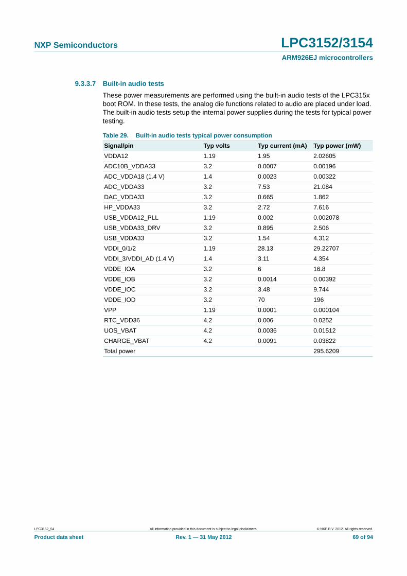
NXP Semiconductors LPC3152/3154ARM926EJ microcontrollers
9.3.3.7 Built-in audio tests
These power measurements are performed using the built-in audio tests of the LPC315x boot ROM. In these tests, the analog die functions related to audio are placed under load. The built-in audio tests setup the internal power supplies during the tests for typical power testing.
Table 29. Built-in audio tests typical power consumption
Signal/pin Typ volts Typ current (mA) Typ power (mW)
VDDA12 1.19 1.95 2.02605
ADC10B_VDDA33 3.2 0.0007 0.00196
ADC_VDDA18 (1.4 V) 1.4 0.0023 0.00322
ADC_VDDA33 3.2 7.53 21.084
DAC_VDDA33 3.2 0.665 1.862
HP_VDDA33 3.2 2.72 7.616
USB_VDDA12_PLL 1.19 0.002 0.002078
USB_VDDA33_DRV 3.2 0.895 2.506
USB_VDDA33 3.2 1.54 4.312
VDDI_0/1/2 1.19 28.13 29.22707
VDDI_3/VDDI_AD (1.4 V) 1.4 3.11 4.354
VDDE_IOA 3.2 6 16.8
VDDE_IOB 3.2 0.0014 0.00392
VDDE_IOC 3.2 3.48 9.744
VDDE_IOD 3.2 70 196
VPP 1.19 0.0001 0.000104
RTC_VDD36 4.2 0.006 0.0252
UOS_VBAT 4.2 0.0036 0.01512
CHARGE_VBAT 4.2 0.0091 0.03822
Total power 295.6209
LPC3152_54 All information provided in this document is subject to legal disclaimers. © NXP B.V. 2012. All rights reserved.
Product data sheet Rev. 1 — 31 May 2012 69 of 94
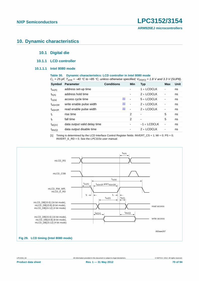
NXP Semiconductors LPC3152/3154ARM926EJ microcontrollers
10. Dynamic characteristics
10.1 Digital die
10.1.1 LCD controller
10.1.1.1 Intel 8080 mode
[1] Timing is determined by the LCD Interface Control Register fields: INVERT_CS = 1; MI = 0; PS = 0; INVERT_E_RD = 0. See the LPC315x user manual.
Table 30. Dynamic characteristics: LCD controller in Intel 8080 modeCL = 25 pF, Tamb = 40 C to +85 C, unless otherwise specified; VDD(IO) = 1.8 V and 3.3 V (SUP8).
Symbol Parameter Conditions Min Typ Max Unit
tsu(A) address set-up time - 1 LCDCLK - ns
th(A) address hold time - 2 LCDCLK - ns
tcy(a) access cycle time [1] - 5 LCDCLK - ns
tw(en)W write enable pulse width [1] - 2 LCDCLK - ns
tw(en)R read enable pulse width [1] - 2 LCDCLK - ns
tr rise time 2 - 5 ns
tf fall time 2 - 5 ns
td(QV) data output valid delay time - 1 LCDCLK - ns
tdis(Q) data output disable time - 2 LCDCLK - ns
Fig 29. LCD timing (Intel 8080 mode)
002aae207
mLCD_RS
mLCD_CSB
mLCD_RW_WR,mLCD_E_RD
mLCD_DB[15:0] (16 bit mode),mLCD_DB[15:8] (8 bit mode),mLCD_DB[15:12] (4 bit mode)
mLCD_DB[15:0] (16 bit mode),mLCD_DB[15:8] (8 bit mode),mLCD_DB[15:12] (4 bit mode)
th(A)
tsu(A) tw(en)R and tw(en)W
td(QV) tdis(Q)
tsu(D) th(D)
tf tr
tcy(a)
read access
write access
LPC3152_54 All information provided in this document is subject to legal disclaimers. © NXP B.V. 2012. All rights reserved.
Product data sheet Rev. 1 — 31 May 2012 70 of 94
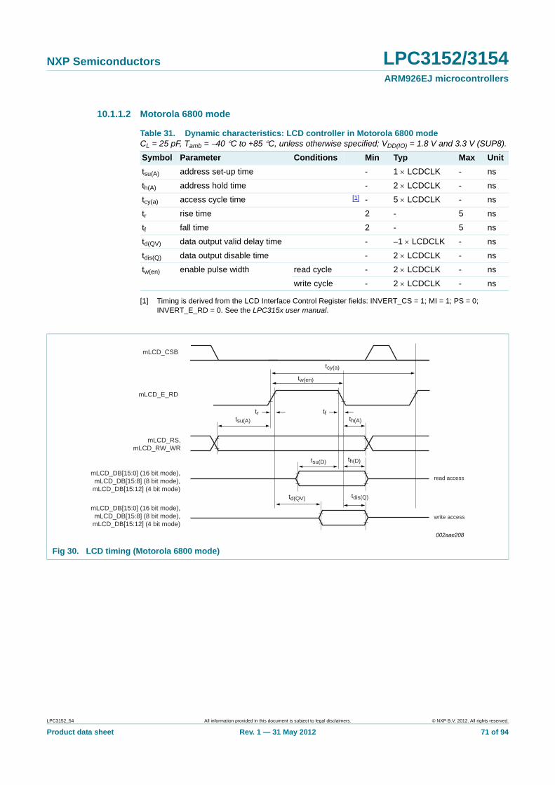
NXP Semiconductors LPC3152/3154ARM926EJ microcontrollers
10.1.1.2 Motorola 6800 mode
[1] Timing is derived from the LCD Interface Control Register fields: INVERT_CS = 1; MI = 1; PS = 0; INVERT_E_RD = 0. See the LPC315x user manual.
Table 31. Dynamic characteristics: LCD controller in Motorola 6800 modeCL = 25 pF, Tamb = 40 C to +85 C, unless otherwise specified; VDD(IO) = 1.8 V and 3.3 V (SUP8).
Symbol Parameter Conditions Min Typ Max Unit
tsu(A) address set-up time - 1 LCDCLK - ns
th(A) address hold time - 2 LCDCLK - ns
tcy(a) access cycle time [1] - 5 LCDCLK - ns
tr rise time 2 - 5 ns
tf fall time 2 - 5 ns
td(QV) data output valid delay time - 1 LCDCLK - ns
tdis(Q) data output disable time - 2 LCDCLK - ns
tw(en) enable pulse width read cycle - 2 LCDCLK - ns
write cycle - 2 LCDCLK - ns
Fig 30. LCD timing (Motorola 6800 mode)
002aae208
mLCD_CSB
mLCD_E_RD
mLCD_RS,mLCD_RW_WR
mLCD_DB[15:0] (16 bit mode),mLCD_DB[15:8] (8 bit mode),mLCD_DB[15:12] (4 bit mode)
mLCD_DB[15:0] (16 bit mode),mLCD_DB[15:8] (8 bit mode),mLCD_DB[15:12] (4 bit mode)
tsu(D)
td(QV)
tsu(A) th(A)
th(D)
tftr
write access
read access
tdis(Q)
tw(en)
tcy(a)
LPC3152_54 All information provided in this document is subject to legal disclaimers. © NXP B.V. 2012. All rights reserved.
Product data sheet Rev. 1 — 31 May 2012 71 of 94
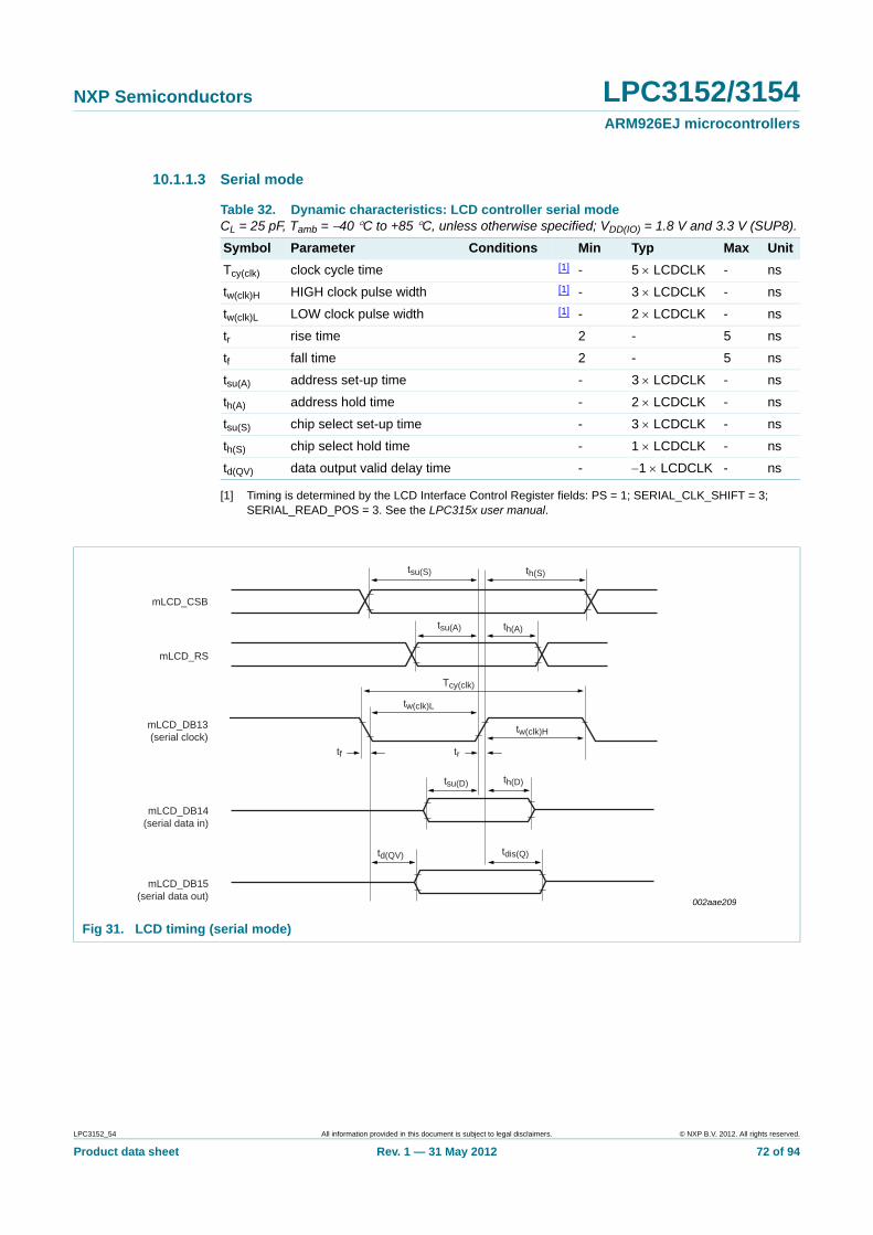
NXP Semiconductors LPC3152/3154ARM926EJ microcontrollers
10.1.1.3 Serial mode
[1] Timing is determined by the LCD Interface Control Register fields: PS = 1; SERIAL_CLK_SHIFT = 3; SERIAL_READ_POS = 3. See the LPC315x user manual.
Table 32. Dynamic characteristics: LCD controller serial modeCL = 25 pF, Tamb = 40 C to +85 C, unless otherwise specified; VDD(IO) = 1.8 V and 3.3 V (SUP8).
Symbol Parameter Conditions Min Typ Max Unit
Tcy(clk) clock cycle time [1] - 5 LCDCLK - ns
tw(clk)H HIGH clock pulse width [1] - 3 LCDCLK - ns
tw(clk)L LOW clock pulse width [1] - 2 LCDCLK - ns
tr rise time 2 - 5 ns
tf fall time 2 - 5 ns
tsu(A) address set-up time - 3 LCDCLK - ns
th(A) address hold time - 2 LCDCLK - ns
tsu(S) chip select set-up time - 3 LCDCLK - ns
th(S) chip select hold time - 1 LCDCLK - ns
td(QV) data output valid delay time - 1 LCDCLK - ns
Fig 31. LCD timing (serial mode)
002aae209
mLCD_CSB
mLCD_RS
mLCD_DB13(serial clock)
mLCD_DB14(serial data in)
mLCD_DB15(serial data out)
tsu(D)
tsu(A) th(A)
tsu(S) th(S)
th(D)
td(QV) tdis(Q)
tf tr
tw(clk)L
tw(clk)H
Tcy(clk)
LPC3152_54 All information provided in this document is subject to legal disclaimers. © NXP B.V. 2012. All rights reserved.
Product data sheet Rev. 1 — 31 May 2012 72 of 94
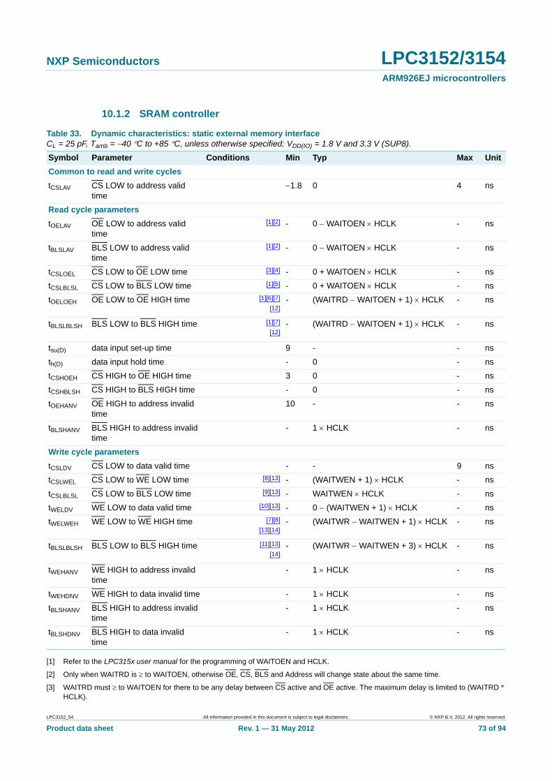
NXP Semiconductors LPC3152/3154ARM926EJ microcontrollers
10.1.2 SRAM controller
[1] Refer to the LPC315x user manual for the programming of WAITOEN and HCLK.
[2] Only when WAITRD is to WAITOEN, otherwise OE, CS, BLS and Address will change state about the same time.
[3] WAITRD must to WAITOEN for there to be any delay between CS active and OE active. The maximum delay is limited to (WAITRD * HCLK).
Table 33. Dynamic characteristics: static external memory interfaceCL = 25 pF, Tamb = 40 C to +85 C, unless otherwise specified; VDD(IO) = 1.8 V and 3.3 V (SUP8).
Symbol Parameter Conditions Min Typ Max Unit
Common to read and write cycles
tCSLAV CS LOW to address valid time
1.8 0 4 ns
Read cycle parameters
tOELAV OE LOW to address valid time
[1][2] - 0 WAITOEN HCLK - ns
tBLSLAV BLS LOW to address valid time
[1][2] - 0 WAITOEN HCLK - ns
tCSLOEL CS LOW to OE LOW time [3][4] - 0 + WAITOEN HCLK - ns
tCSLBLSL CS LOW to BLS LOW time [1][5] - 0 + WAITOEN HCLK - ns
tOELOEH OE LOW to OE HIGH time [1][6][7]
[12]- (WAITRD WAITOEN + 1) HCLK - ns
tBLSLBLSH BLS LOW to BLS HIGH time [1][7]
[12]- (WAITRD WAITOEN + 1) HCLK - ns
tsu(D) data input set-up time 9 - - ns
th(D) data input hold time - 0 - ns
tCSHOEH CS HIGH to OE HIGH time 3 0 - ns
tCSHBLSH CS HIGH to BLS HIGH time - 0 - ns
tOEHANV OE HIGH to address invalid time
10 - - ns
tBLSHANV BLS HIGH to address invalid time
- 1 HCLK - ns
Write cycle parameters
tCSLDV CS LOW to data valid time - - 9 ns
tCSLWEL CS LOW to WE LOW time [8][13] - (WAITWEN + 1) HCLK - ns
tCSLBLSL CS LOW to BLS LOW time [9][13] - WAITWEN HCLK - ns
tWELDV WE LOW to data valid time [10][13] - 0 (WAITWEN + 1) HCLK - ns
tWELWEH WE LOW to WE HIGH time [7][8]
[13][14]- (WAITWR WAITWEN + 1) HCLK - ns
tBLSLBLSH BLS LOW to BLS HIGH time [11][13]
[14]- (WAITWR WAITWEN + 3) HCLK - ns
tWEHANV WE HIGH to address invalid time
- 1 HCLK - ns
tWEHDNV WE HIGH to data invalid time - 1 HCLK - ns
tBLSHANV BLS HIGH to address invalid time
- 1 HCLK - ns
tBLSHDNV BLS HIGH to data invalid time
- 1 HCLK - ns
LPC3152_54 All information provided in this document is subject to legal disclaimers. © NXP B.V. 2012. All rights reserved.
Product data sheet Rev. 1 — 31 May 2012 73 of 94
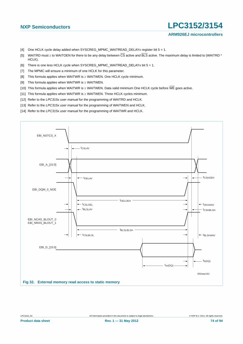
NXP Semiconductors LPC3152/3154ARM926EJ microcontrollers
[4] One HCLK cycle delay added when SYSCREG_MPMC_WAITREAD_DELAYx register bit 5 = 1.
[5] WAITRD must to WAITOEN for there to be any delay between CS active and BLS active. The maximum delay is limited to (WAITRD * HCLK).
[6] There is one less HCLK cycle when SYSCREG_MPMC_WAITREAD_DELAYx bit 5 = 1.
[7] The MPMC will ensure a minimum of one HCLK for this parameter.
[8] This formula applies when WAITWR is WAITWEN. One HCLK cycle minimum.
[9] This formula applies when WAITWR is WAITWEN.
[10] This formula applies when WAITWR is WAITWEN. Data valid minimum One HCLK cycle before WE goes active.
[11] This formula applies when WAITWR is WAITWEN. Three HCLK cycles minimum.
[12] Refer to the LPC315x user manual for the programming of WAITRD and HCLK.
[13] Refer to the LPC315x user manual for the programming of WAITWEN and HCLK.
[14] Refer to the LPC315x user manual for the programming of WAITWR and HCLK.
Fig 32. External memory read access to static memory
tCSHOEH
tCSHBLSH
tOEHANV
tBLSHANV
tCSLOEL
tOELOEH
tCSLBLSL
tBLSLBLSH
tCSLAV
tOELAV
tBLSLAV
th(DQ)
tsu(DQ)
EBI_NSTCS_X
EBI_DQM_0_NOE
EBI_NCAS_BLOUT_0EBI_NRAS_BLOUT_1
EBI_A_[15:0]
EBI_D_[15:0]
002aae161
LPC3152_54 All information provided in this document is subject to legal disclaimers. © NXP B.V. 2012. All rights reserved.
Product data sheet Rev. 1 — 31 May 2012 74 of 94
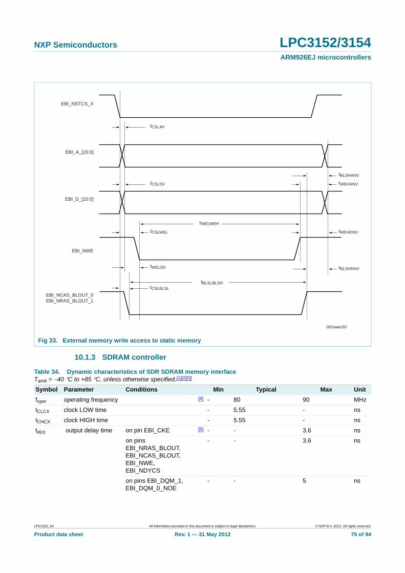
NXP Semiconductors LPC3152/3154ARM926EJ microcontrollers
10.1.3 SDRAM controller
Fig 33. External memory write access to static memory
tBLSLBLSH
tCSLAV
tCSLDV tWEHANV
tCSLWEL
tCSLBLSL
tWEHDNV
tBLSHDNV
tBLSHANV
tWELWEH
tWELDV
002aae162
EBI_NSTCS_X
EBI_NCAS_BLOUT_0EBI_NRAS_BLOUT_1
EBI_A_[15:0]
EBI_D_[15:0]
EBI_NWE
Table 34. Dynamic characteristics of SDR SDRAM memory interface Tamb = 40 C to +85 C, unless otherwise specified.[1][2][3]
Symbol Parameter Conditions Min Typical Max Unit
foper operating frequency [4] - 80 90 MHz
tCLCX clock LOW time - 5.55 - ns
tCHCX clock HIGH time - 5.55 - ns
td(o) output delay time on pin EBI_CKE [5] - - 3.6 ns
on pins EBI_NRAS_BLOUT, EBI_NCAS_BLOUT, EBI_NWE, EBI_NDYCS
- - 3.6 ns
on pins EBI_DQM_1, EBI_DQM_0_NOE
- - 5 ns
LPC3152_54 All information provided in this document is subject to legal disclaimers. © NXP B.V. 2012. All rights reserved.
Product data sheet Rev. 1 — 31 May 2012 75 of 94
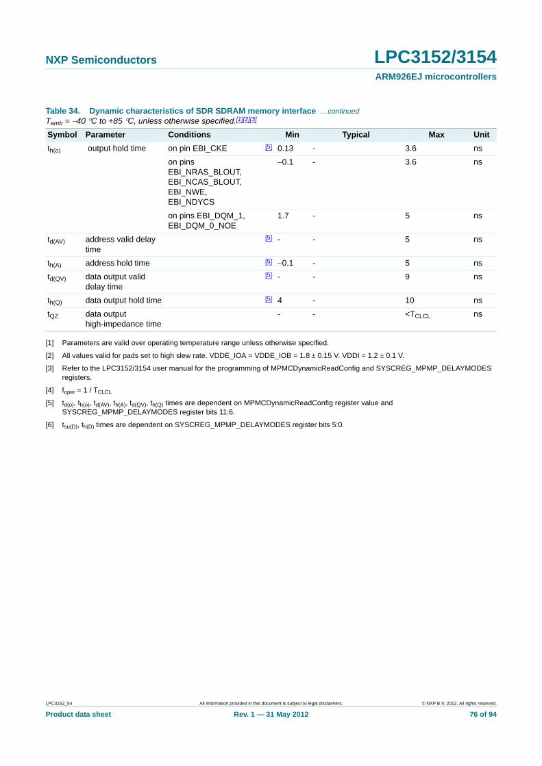
NXP Semiconductors LPC3152/3154ARM926EJ microcontrollers
[1] Parameters are valid over operating temperature range unless otherwise specified.
[2] All values valid for pads set to high slew rate. VDDE_IOA = VDDE_IOB = 1.8 0.15 V. VDDI = 1.2 0.1 V.
[3] Refer to the LPC3152/3154 user manual for the programming of MPMCDynamicReadConfig and SYSCREG_MPMP_DELAYMODES registers.
[4] foper = 1 / TCLCL
[5] td(o), th(o), td(AV), th(A), td(QV), th(Q) times are dependent on MPMCDynamicReadConfig register value and SYSCREG_MPMP_DELAYMODES register bits 11:6.
[6] tsu(D), th(D) times are dependent on SYSCREG_MPMP_DELAYMODES register bits 5:0.
th(o) output hold time on pin EBI_CKE [5] 0.13 - 3.6 ns
on pins EBI_NRAS_BLOUT, EBI_NCAS_BLOUT, EBI_NWE, EBI_NDYCS
0.1 - 3.6 ns
on pins EBI_DQM_1, EBI_DQM_0_NOE
1.7 - 5 ns
td(AV) address valid delay time
[5] - - 5 ns
th(A) address hold time [5] 0.1 - 5 ns
td(QV) data output valid delay time
[5] - - 9 ns
th(Q) data output hold time [5] 4 - 10 ns
tQZ data output high-impedance time
- - <TCLCL ns
Table 34. Dynamic characteristics of SDR SDRAM memory interface …continuedTamb = 40 C to +85 C, unless otherwise specified.[1][2][3]
Symbol Parameter Conditions Min Typical Max Unit
LPC3152_54 All information provided in this document is subject to legal disclaimers. © NXP B.V. 2012. All rights reserved.
Product data sheet Rev. 1 — 31 May 2012 76 of 94
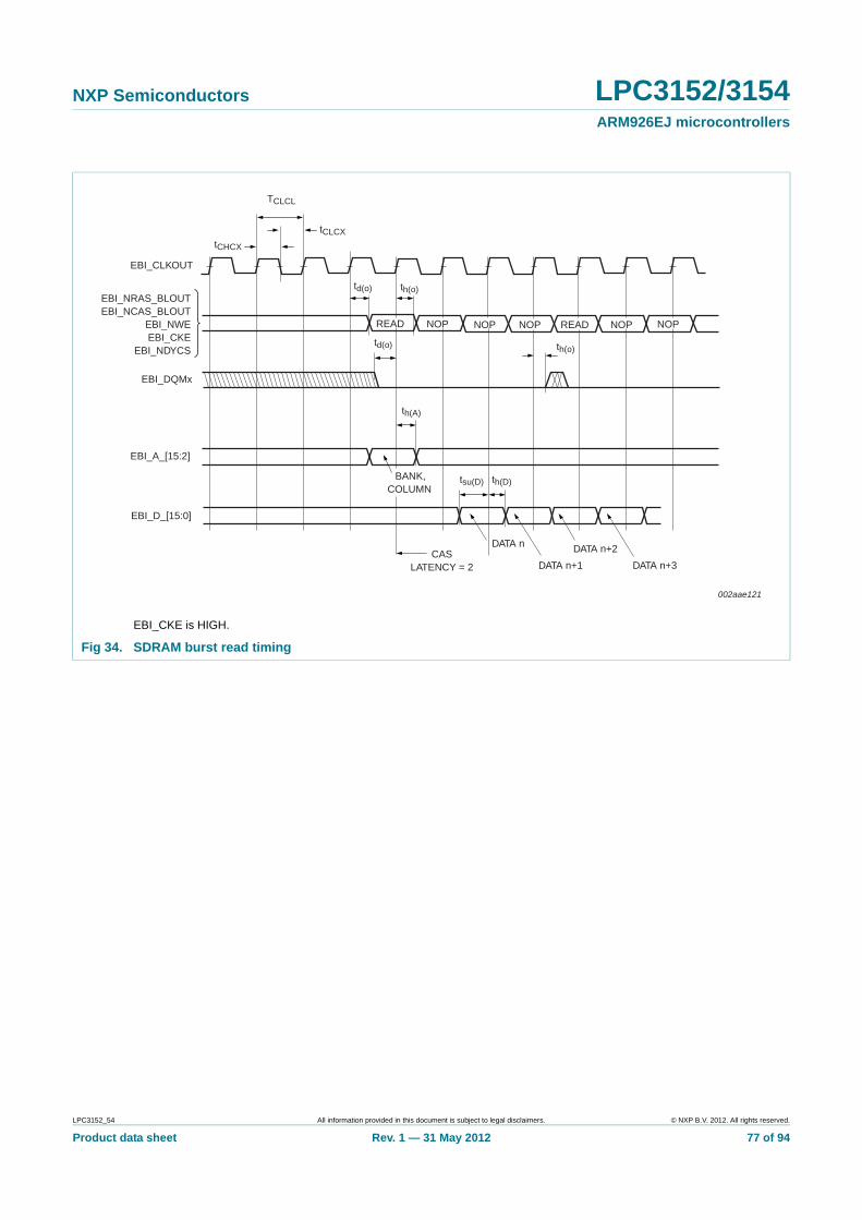
NXP Semiconductors LPC3152/3154ARM926EJ microcontrollers
EBI_CKE is HIGH.
Fig 34. SDRAM burst read timing
EBI_A_[15:2]
EBI_DQMx
EBI_D_[15:0]
EBI_CLKOUT
EBI_NRAS_BLOUTEBI_NCAS_BLOUT
EBI_NWEEBI_CKE
EBI_NDYCS
th(o)
th(o)
th(A)
tsu(D) th(D)
READ NOP NOP NOP NOP NOPREAD
BANK,COLUMN
002aae121
TCLCL
tCHCX
tCLCX
td(o)
td(o)
CASLATENCY = 2
DATA n
DATA n+1
DATA n+2
DATA n+3
LPC3152_54 All information provided in this document is subject to legal disclaimers. © NXP B.V. 2012. All rights reserved.
Product data sheet Rev. 1 — 31 May 2012 77 of 94
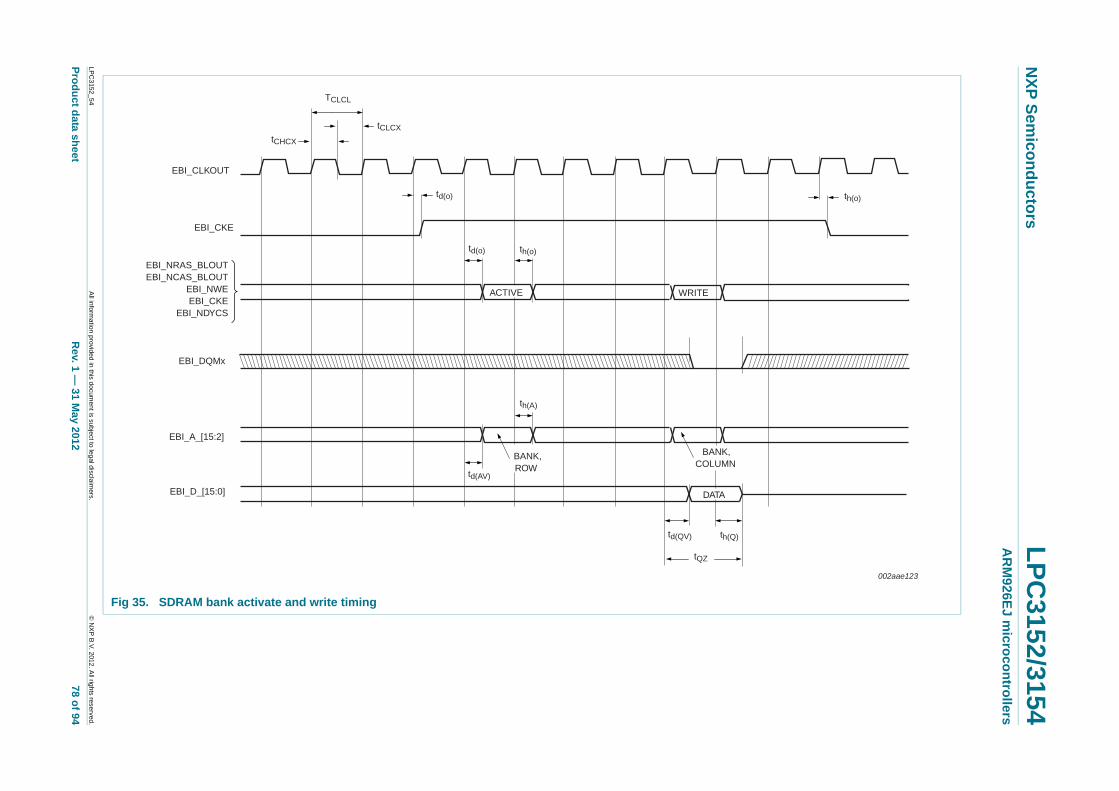
xxxxxxxxxxxxxxxxxxxxx xxxxxxxxxxxxxxxxxxxxxxxxxx xxxxxxx x x x xxxxxxxxxxxxxxxxxxxxxxxxxxxxxx xxxxxxxxxxxxxxxxxxx xx xx xxxxx xxxxxxxxxxxxxxxxxxxxxxxxxxx xxxxxxxxxxxxxxxxxxx xxxxxx xxxxxxxxxxxxxxxxxxxxxxxxxxxxxxxxxxx xxxxxxxxxxxx x x xxxxxxxxxxxxxxxxxxxxx xxxxxxxxxxxxxxxxxxxxxxxxxxxxxx xxxxx xxxxxxxxxxxxxxxxxxxxxxxxxxxxxxxxxxxxxxxxxxxxxxxxxx xxxxxxxx xxxxxxxxxxxxxxxxxxxxxxxxx xxxxxxxxxxxxxxxxxxxx xxx
LPC
3152_54
Pro
du
ct data sh
NX
P S
emico
nd
ucto
rsL
PC
3152/3154A
RM
926
EJ m
icro
co
ntro
llers
002aae123
TCLCL
tCHCX
tCLCX
th(o)
All inform
ation provided
in this docum
ent is subject to leg
al disclaim
ers.©
NX
P B
.V. 2012. A
ll rights reserved.
eetR
ev. 1 — 31 M
ay 2012
78 of 94
Fig 35. SDRAM bank activate and write timing
EBI_CKE
WRITE
BANK,ROW
BANK,COLUMN
EBI_A_[15:2]
EBI_D_[15:0]
EBI_CLKOUT
EBI_NRAS_BLOUTEBI_NCAS_BLOUT
EBI_NWEEBI_CKE
EBI_NDYCS
th(o)
td(o)
td(o)
td(AV)
td(QV)
th(A)
th(Q)
EBI_DQMx
tQZ
ACTIVE
DATA
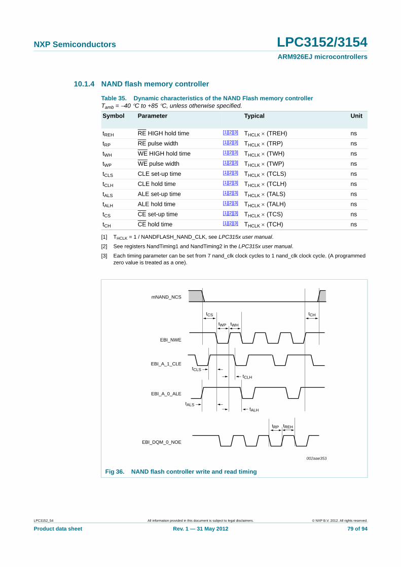
NXP Semiconductors LPC3152/3154ARM926EJ microcontrollers
10.1.4 NAND flash memory controller
[1] THCLK = 1 / NANDFLASH_NAND_CLK, see LPC315x user manual.
[2] See registers NandTiming1 and NandTiming2 in the LPC315x user manual.
[3] Each timing parameter can be set from 7 nand_clk clock cycles to 1 nand_clk clock cycle. (A programmed zero value is treated as a one).
Table 35. Dynamic characteristics of the NAND Flash memory controllerTamb = 40 C to +85 C, unless otherwise specified.
Symbol Parameter Typical Unit
tREH RE HIGH hold time [1][2][3] THCLK (TREH) ns
tRP RE pulse width [1][2][3] THCLK (TRP) ns
tWH WE HIGH hold time [1][2][3] THCLK (TWH) ns
tWP WE pulse width [1][2][3] THCLK (TWP) ns
tCLS CLE set-up time [1][2][3] THCLK (TCLS) ns
tCLH CLE hold time [1][2][3] THCLK (TCLH) ns
tALS ALE set-up time [1][2][3] THCLK (TALS) ns
tALH ALE hold time [1][2][3] THCLK (TALH) ns
tCS CE set-up time [1][2][3] THCLK (TCS) ns
tCH CE hold time [1][2][3] THCLK (TCH) ns
Fig 36. NAND flash controller write and read timing
EBI_NWE
EBI_A_1_CLE
EBI_A_0_ALE
tWP
tCS tCH
tCLS
tCLH
mNAND_NCS
tWH
002aae353
tALStALH
tRP tREH
EBI_DQM_0_NOE
LPC3152_54 All information provided in this document is subject to legal disclaimers. © NXP B.V. 2012. All rights reserved.
Product data sheet Rev. 1 — 31 May 2012 79 of 94
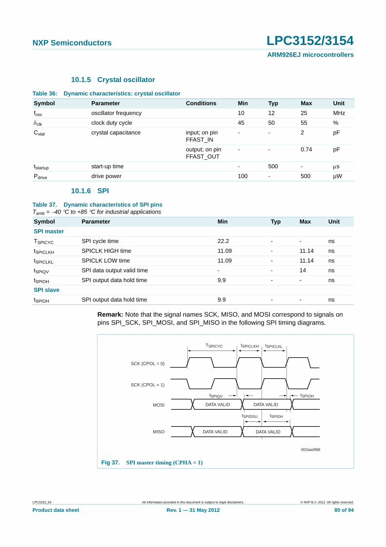
NXP Semiconductors LPC3152/3154ARM926EJ microcontrollers
10.1.5 Crystal oscillator
10.1.6 SPI
Remark: Note that the signal names SCK, MISO, and MOSI correspond to signals on pins SPI_SCK, SPI_MOSI, and SPI_MISO in the following SPI timing diagrams.
Table 36: Dynamic characteristics: crystal oscillator
Symbol Parameter Conditions Min Typ Max Unit
fosc oscillator frequency 10 12 25 MHz
clk clock duty cycle 45 50 55 %
Cxtal crystal capacitance input; on pin FFAST_IN
- - 2 pF
output; on pin FFAST_OUT
- - 0.74 pF
tstartup start-up time - 500 - s
Pdrive drive power 100 - 500 µW
Table 37. Dynamic characteristics of SPI pinsTamb = 40 C to +85 C for industrial applications
Symbol Parameter Min Typ Max Unit
SPI master
TSPICYC SPI cycle time 22.2 - - ns
tSPICLKH SPICLK HIGH time 11.09 - 11.14 ns
tSPICLKL SPICLK LOW time 11.09 - 11.14 ns
tSPIQV SPI data output valid time - - 14 ns
tSPIOH SPI output data hold time 9.9 - - ns
SPI slave
tSPIOH SPI output data hold time 9.9 - - ns
Fig 37. SPI master timing (CPHA = 1)
SCK (CPOL = 0)
MOSI
MISO
002aad986
TSPICYC tSPICLKH tSPICLKL
tSPIDSU tSPIDH
tSPIQV
DATA VALID DATA VALID
tSPIOH
SCK (CPOL = 1)
DATA VALID DATA VALID
LPC3152_54 All information provided in this document is subject to legal disclaimers. © NXP B.V. 2012. All rights reserved.
Product data sheet Rev. 1 — 31 May 2012 80 of 94
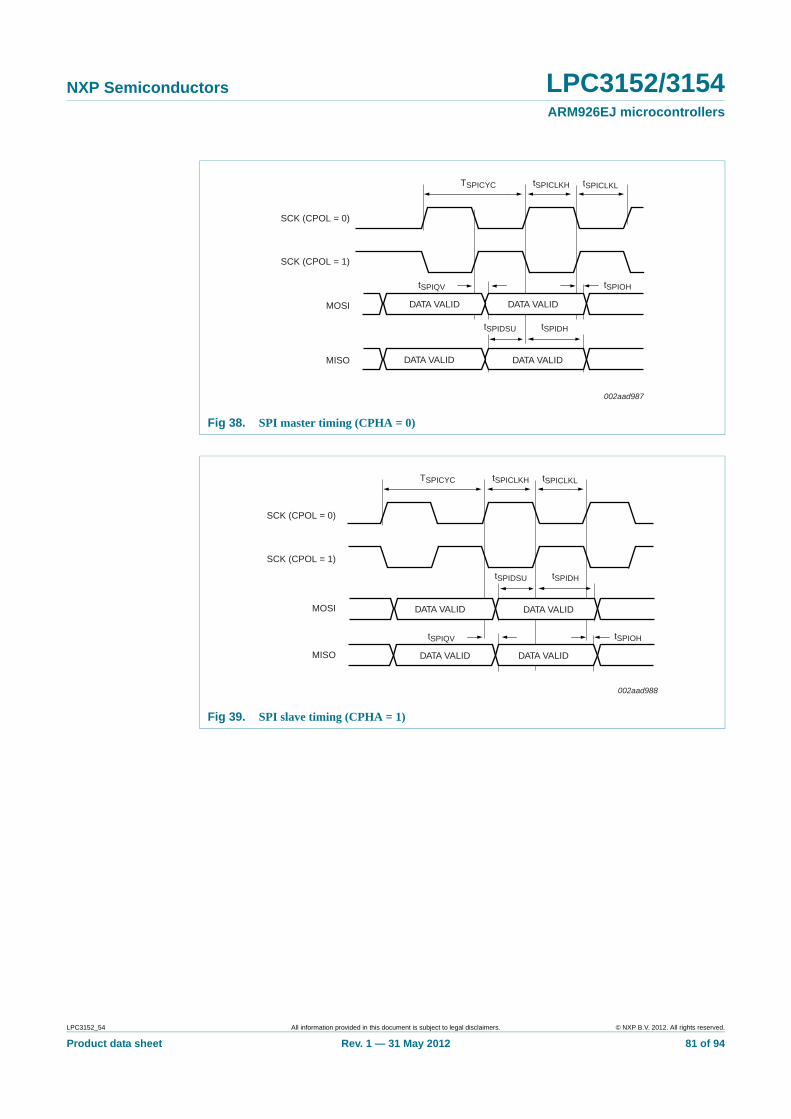
NXP Semiconductors LPC3152/3154ARM926EJ microcontrollers
Fig 38. SPI master timing (CPHA = 0)
Fig 39. SPI slave timing (CPHA = 1)
SCK (CPOL = 0)
MOSI
MISO
002aad987
TSPICYC tSPICLKH tSPICLKL
tSPIDSU tSPIDH
DATA VALID DATA VALID
tSPIOH
SCK (CPOL = 1)
DATA VALID DATA VALID
tSPIQV
SCK (CPOL = 0)
MOSI
MISO
002aad988
TSPICYC tSPICLKH tSPICLKL
tSPIDSU tSPIDH
tSPIQV
DATA VALID DATA VALID
tSPIOH
SCK (CPOL = 1)
DATA VALID DATA VALID
LPC3152_54 All information provided in this document is subject to legal disclaimers. © NXP B.V. 2012. All rights reserved.
Product data sheet Rev. 1 — 31 May 2012 81 of 94
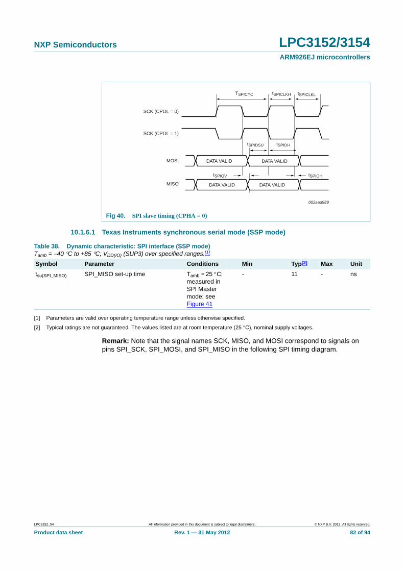
NXP Semiconductors LPC3152/3154ARM926EJ microcontrollers
10.1.6.1 Texas Instruments synchronous serial mode (SSP mode)
[1] Parameters are valid over operating temperature range unless otherwise specified.
[2] Typical ratings are not guaranteed. The values listed are at room temperature (25 C), nominal supply voltages.
Remark: Note that the signal names SCK, MISO, and MOSI correspond to signals on pins SPI_SCK, SPI_MOSI, and SPI_MISO in the following SPI timing diagram.
Fig 40. SPI slave timing (CPHA = 0)
SCK (CPOL = 0)
MOSI
MISO
002aad989
TSPICYC tSPICLKH tSPICLKL
tSPIDSU tSPIDH
tSPIQV
DATA VALID DATA VALID
tSPIOH
SCK (CPOL = 1)
DATA VALID DATA VALID
Table 38. Dynamic characteristic: SPI interface (SSP mode)Tamb = 40 C to +85 C; VDD(IO) (SUP3) over specified ranges.[1]
Symbol Parameter Conditions Min Typ[2] Max Unit
tsu(SPI_MISO) SPI_MISO set-up time Tamb = 25 C; measured in SPI Master mode; see Figure 41
- 11 - ns
LPC3152_54 All information provided in this document is subject to legal disclaimers. © NXP B.V. 2012. All rights reserved.
Product data sheet Rev. 1 — 31 May 2012 82 of 94
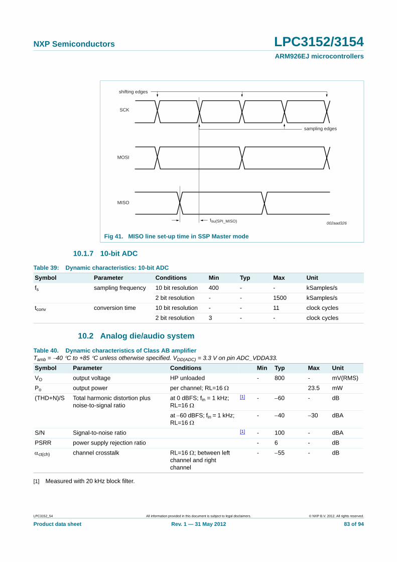
NXP Semiconductors LPC3152/3154ARM926EJ microcontrollers
10.1.7 10-bit ADC
10.2 Analog die/audio system
[1] Measured with 20 kHz block filter.
Fig 41. MISO line set-up time in SSP Master mode
tsu(SPI_MISO)
SCK
shifting edges
MOSI
MISO
002aad326
sampling edges
Table 39: Dynamic characteristics: 10-bit ADC
Symbol Parameter Conditions Min Typ Max Unit
fs sampling frequency 10 bit resolution 400 - - kSamples/s
2 bit resolution - - 1500 kSamples/s
tconv conversion time 10 bit resolution - - 11 clock cycles
2 bit resolution 3 - - clock cycles
Table 40. Dynamic characteristics of Class AB amplifierTamb = 40 C to +85 C unless otherwise specified. VDD(ADC) = 3.3 V on pin ADC_VDDA33.
Symbol Parameter Conditions Min Typ Max Unit
VO output voltage HP unloaded - 800 - mV(RMS)
Po output power per channel; RL=16 23.5 mW
(THD+N)/S Total harmonic distortion plus noise-to-signal ratio
at 0 dBFS; fin = 1 kHz; RL=16
[1] - 60 - dB
at 60 dBFS; fin = 1 kHz; RL=16
- 40 30 dBA
S/N Signal-to-noise ratio [1] - 100 - dBA
PSRR power supply rejection ratio - 6 - dB
ct(ch) channel crosstalk RL=16 ; between left channel and right channel
- 55 - dB
LPC3152_54 All information provided in this document is subject to legal disclaimers. © NXP B.V. 2012. All rights reserved.
Product data sheet Rev. 1 — 31 May 2012 83 of 94
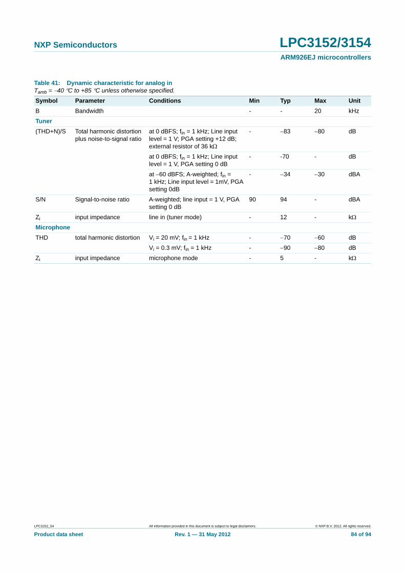
NXP Semiconductors LPC3152/3154ARM926EJ microcontrollers
Table 41: Dynamic characteristic for analog in Tamb = 40 C to +85 C unless otherwise specified.
Symbol Parameter Conditions Min Typ Max Unit
B Bandwidth - - 20 kHz
Tuner
(THD+N)/S Total harmonic distortion plus noise-to-signal ratio
at 0 dBFS; fin = 1 kHz; Line input level = 1 V; PGA setting +12 dB; external resistor of 36 k
- 83 80 dB
at 0 dBFS; fin = 1 kHz; Line input level = 1 V, PGA setting 0 dB
- -70 - dB
at 60 dBFS; A-weighted; fin = 1 kHz; Line input level = 1mV, PGA setting 0dB
- 34 30 dBA
S/N Signal-to-noise ratio A-weighted; line input = 1 V, PGA setting 0 dB
90 94 - dBA
Zi input impedance line in (tuner mode) - 12 - k
Microphone
THD total harmonic distortion Vi = 20 mV; fin = 1 kHz - 70 60 dB
Vi = 0.3 mV; fin = 1 kHz - 90 80 dB
Zi input impedance microphone mode - 5 - k
LPC3152_54 All information provided in this document is subject to legal disclaimers. © NXP B.V. 2012. All rights reserved.
Product data sheet Rev. 1 — 31 May 2012 84 of 94
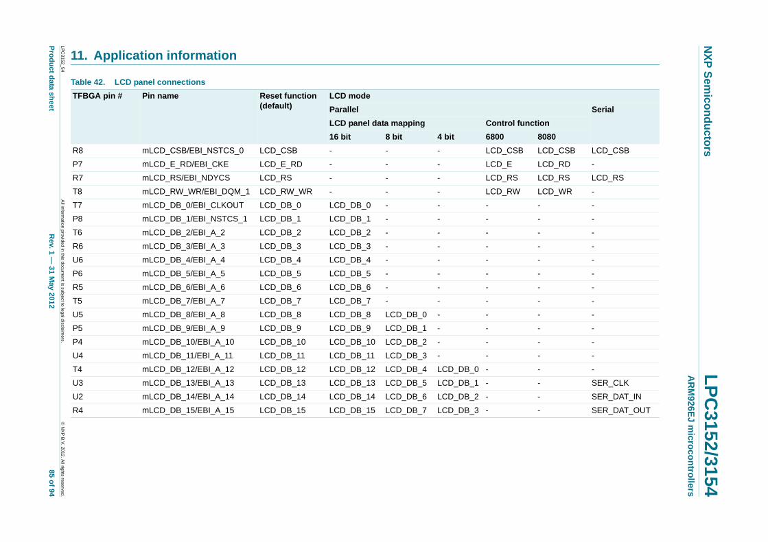
xxxxxxxxxxxxxxxxxxxxx xxxxxxxxxxxxxxxxxxxxxxxxxx xxxxxxx x x x xxxxxxxxxxxxxxxxxxxxxxxxxxxxxx xxxxxxxxxxxxxxxxxxx xx xx xxxxx xxxxxxxxxxxxxxxxxxxxxxxxxxx xxxxxxxxxxxxxxxxxxx xxxxxx xxxxxxxxxxxxxxxxxxxxxxxxxxxxxxxxxxx xxxxxxxxxxxx x x xxxxxxxxxxxxxxxxxxxxx xxxxxxxxxxxxxxxxxxxxxxxxxxxxxx xxxxx xxxxxxxxxxxxxxxxxxxxxxxxxxxxxxxxxxxxxxxxxxxxxxxxxx xxxxxxxx xxxxxxxxxxxxxxxxxxxxxxxxx xxxxxxxxxxxxxxxxxxxx xxx
LPC
3152_54
Pro
du
ct data sh
NX
P S
emico
nd
ucto
rsL
PC
3152/3154A
RM
926
EJ m
icro
co
ntro
llers
11. Application information
Table 42. LCD panel connections
TFBGA pin # Pin name Reset function LCD mode
Serial
ol function
8080
CSB LCD_CSB LCD_CSB
E LCD_RD -
RS LCD_RS LCD_RS
RW LCD_WR -
- -
- -
- -
- -
- -
- -
- -
- -
- -
- -
- -
- -
- -
- SER_CLK
- SER_DAT_IN
- SER_DAT_OUT
All inform
ation provided
in this docum
ent is subject to leg
al disclaim
ers.©
NX
P B
.V. 2012. A
ll rights reserved.
eetR
ev. 1 — 31 M
ay 2012
85 of 94
(default) Parallel
LCD panel data mapping Contr
16 bit 8 bit 4 bit 6800
R8 mLCD_CSB/EBI_NSTCS_0 LCD_CSB - - - LCD_
P7 mLCD_E_RD/EBI_CKE LCD_E_RD - - - LCD_
R7 mLCD_RS/EBI_NDYCS LCD_RS - - - LCD_
T8 mLCD_RW_WR/EBI_DQM_1 LCD_RW_WR - - - LCD_
T7 mLCD_DB_0/EBI_CLKOUT LCD_DB_0 LCD_DB_0 - - -
P8 mLCD_DB_1/EBI_NSTCS_1 LCD_DB_1 LCD_DB_1 - - -
T6 mLCD_DB_2/EBI_A_2 LCD_DB_2 LCD_DB_2 - - -
R6 mLCD_DB_3/EBI_A_3 LCD_DB_3 LCD_DB_3 - - -
U6 mLCD_DB_4/EBI_A_4 LCD_DB_4 LCD_DB_4 - - -
P6 mLCD_DB_5/EBI_A_5 LCD_DB_5 LCD_DB_5 - - -
R5 mLCD_DB_6/EBI_A_6 LCD_DB_6 LCD_DB_6 - - -
T5 mLCD_DB_7/EBI_A_7 LCD_DB_7 LCD_DB_7 - - -
U5 mLCD_DB_8/EBI_A_8 LCD_DB_8 LCD_DB_8 LCD_DB_0 - -
P5 mLCD_DB_9/EBI_A_9 LCD_DB_9 LCD_DB_9 LCD_DB_1 - -
P4 mLCD_DB_10/EBI_A_10 LCD_DB_10 LCD_DB_10 LCD_DB_2 - -
U4 mLCD_DB_11/EBI_A_11 LCD_DB_11 LCD_DB_11 LCD_DB_3 - -
T4 mLCD_DB_12/EBI_A_12 LCD_DB_12 LCD_DB_12 LCD_DB_4 LCD_DB_0 -
U3 mLCD_DB_13/EBI_A_13 LCD_DB_13 LCD_DB_13 LCD_DB_5 LCD_DB_1 -
U2 mLCD_DB_14/EBI_A_14 LCD_DB_14 LCD_DB_14 LCD_DB_6 LCD_DB_2 -
R4 mLCD_DB_15/EBI_A_15 LCD_DB_15 LCD_DB_15 LCD_DB_7 LCD_DB_3 -
NXP Semiconductors LPC3152/3154ARM926EJ microcontrollers
12. Marking
Table 43. LPC3152/3154 Marking
Line Marking Description
A LPC3152/3154 BASIC_TYPE
LPC3152_54 All information provided in this document is subject to legal disclaimers. © NXP B.V. 2012. All rights reserved.
Product data sheet Rev. 1 — 31 May 2012 86 of 94
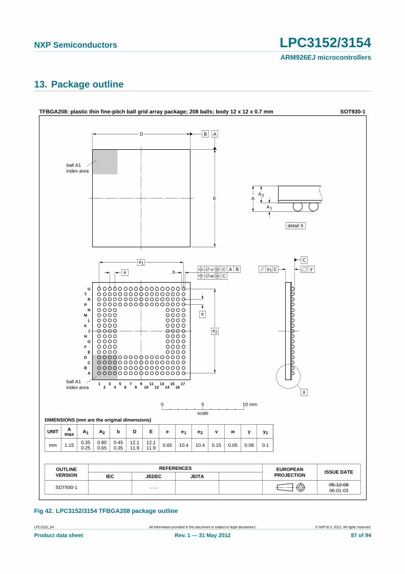
NXP Semiconductors LPC3152/3154ARM926EJ microcontrollers
13. Package outline
Fig 42. LPC3152/3154 TFBGA208 package outline
REFERENCESOUTLINEVERSION
EUROPEANPROJECTION
ISSUE DATEIEC JEDEC JEITA
SOT930-1 - - -
SOT930-1
05-12-0806-01-03
DIMENSIONS (mm are the original dimensions)
TFBGA208: plastic thin fine-pitch ball grid array package; 208 balls; body 12 x 12 x 0.7 mm
0 5 10 mm
scale
UNIT
mm 0.350.25
0.800.65
0.450.35
12.111.9
A1 A2 b E
12.111.9
D e e1 v
0.1510.4
e2
10.40.65
w
0.05
y
0.08
y1
0.1
Amax
1.15
ball A1index area
D
E
B A
b
ball A1index area
e2
e1
e
e
AC B∅ v M
C∅ w M
AB
CD
EF
H
K
G
J
LM
NP
RT
U
2 4 6 8 10 12 14 161 3 5 7 9 11 13 15 17
C
yCy1
X
A
detail X
A2
A1
LPC3152_54 All information provided in this document is subject to legal disclaimers. © NXP B.V. 2012. All rights reserved.
Product data sheet Rev. 1 — 31 May 2012 87 of 94
NXP Semiconductors LPC3152/3154ARM926EJ microcontrollers
14. Abbreviations
Table 44: Abbreviations
Acronym Description
ADC Analog-to-Digital Converter
ADC10B 10 Bit Analogue to Digital Converter
AES Advanced Encryption Standard
AVC Analog Volume Control
BIU Bus Interface Unit
CBC Cipher Block Chaining
CD Compact Disk
CGU Clock Generation Unit
DFU Device Firmware Upgrade
DMA Direct Memory Access Controller
DRM Digital Rights Management
ECC Error Correction Code
FIR Finite Input Response
HP Headphones
IOCONFIG Input Output Configuration
ROM Read Only Memory
IrDA Infrared Data Association
JTAG Joint Test Action Group
ISRAM Internal Static RAM Memory
JTAG Joint Test Action Group
LCD Liquid Crystal Display
LDO Low Drop voltage Output regulator
LNA Low-Noise Amplifier
MMU Memory Management Unit
NTC Negative Temperature Coefficient
OTP One-Time Programmable Memory
PCM Pulse Code Modulation
PGA Programmable Gain Amplifier
PHY Physical Layer
PLL Phase Locked Loop
PSU Power Supply Unit
PWM Pulse Width Modulation
RNG Random Number Generator
SDC
SHA1 Secure Hash Algorithm 1
SIR Serial IrDA
SPI Serial Peripheral Interface
SSI Serial Synchronous Interface
SysCReg System Control Registers
LPC3152_54 All information provided in this document is subject to legal disclaimers. © NXP B.V. 2012. All rights reserved.
Product data sheet Rev. 1 — 31 May 2012 88 of 94
NXP Semiconductors LPC3152/3154ARM926EJ microcontrollers
Timer Timer module
UART Universal Asynchronous Receiver Transmitter
USB 2.0 HS OTG Universal Serial Bus 2.0 High-Speed On-The-Go
Table 44: Abbreviations …continued
Acronym Description
LPC3152_54 All information provided in this document is subject to legal disclaimers. © NXP B.V. 2012. All rights reserved.
Product data sheet Rev. 1 — 31 May 2012 89 of 94
NXP Semiconductors LPC3152/3154ARM926EJ microcontrollers
15. Revision history
Table 45: Revision history
Document ID Release date Data sheet status Change notice Supersedes
LPC3152_54 20120531 Product data sheet - -
LPC3152_54 All information provided in this document is subject to legal disclaimers. © NXP B.V. 2012. All rights reserved.
Product data sheet Rev. 1 — 31 May 2012 90 of 94
NXP Semiconductors LPC3152/3154ARM926EJ microcontrollers
16. Legal information
16.1 Data sheet status
[1] Please consult the most recently issued document before initiating or completing a design.
[2] The term ‘short data sheet’ is explained in section “Definitions”.
[3] The product status of device(s) described in this document may have changed since this document was published and may differ in case of multiple devices. The latest product status information is available on the Internet at URL http://www.nxp.com.
16.2 Definitions
Draft — The document is a draft version only. The content is still under internal review and subject to formal approval, which may result in modifications or additions. NXP Semiconductors does not give any representations or warranties as to the accuracy or completeness of information included herein and shall have no liability for the consequences of use of such information.
Short data sheet — A short data sheet is an extract from a full data sheet with the same product type number(s) and title. A short data sheet is intended for quick reference only and should not be relied upon to contain detailed and full information. For detailed and full information see the relevant full data sheet, which is available on request via the local NXP Semiconductors sales office. In case of any inconsistency or conflict with the short data sheet, the full data sheet shall prevail.
Product specification — The information and data provided in a Product data sheet shall define the specification of the product as agreed between NXP Semiconductors and its customer, unless NXP Semiconductors and customer have explicitly agreed otherwise in writing. In no event however, shall an agreement be valid in which the NXP Semiconductors product is deemed to offer functions and qualities beyond those described in the Product data sheet.
16.3 Disclaimers
Limited warranty and liability — Information in this document is believed to be accurate and reliable. However, NXP Semiconductors does not give any representations or warranties, expressed or implied, as to the accuracy or completeness of such information and shall have no liability for the consequences of use of such information. NXP Semiconductors takes no responsibility for the content in this document if provided by an information source outside of NXP Semiconductors.
In no event shall NXP Semiconductors be liable for any indirect, incidental, punitive, special or consequential damages (including - without limitation - lost profits, lost savings, business interruption, costs related to the removal or replacement of any products or rework charges) whether or not such damages are based on tort (including negligence), warranty, breach of contract or any other legal theory.
Notwithstanding any damages that customer might incur for any reason whatsoever, NXP Semiconductors’ aggregate and cumulative liability towards customer for the products described herein shall be limited in accordance with the Terms and conditions of commercial sale of NXP Semiconductors.
Right to make changes — NXP Semiconductors reserves the right to make changes to information published in this document, including without limitation specifications and product descriptions, at any time and without notice. This document supersedes and replaces all information supplied prior to the publication hereof.
Suitability for use — NXP Semiconductors products are not designed, authorized or warranted to be suitable for use in life support, life-critical or safety-critical systems or equipment, nor in applications where failure or malfunction of an NXP Semiconductors product can reasonably be expected to result in personal injury, death or severe property or environmental damage. NXP Semiconductors and its suppliers accept no liability for inclusion and/or use of NXP Semiconductors products in such equipment or applications and therefore such inclusion and/or use is at the customer’s own risk.
Applications — Applications that are described herein for any of these products are for illustrative purposes only. NXP Semiconductors makes no representation or warranty that such applications will be suitable for the specified use without further testing or modification.
Customers are responsible for the design and operation of their applications and products using NXP Semiconductors products, and NXP Semiconductors accepts no liability for any assistance with applications or customer product design. It is customer’s sole responsibility to determine whether the NXP Semiconductors product is suitable and fit for the customer’s applications and products planned, as well as for the planned application and use of customer’s third party customer(s). Customers should provide appropriate design and operating safeguards to minimize the risks associated with their applications and products.
NXP Semiconductors does not accept any liability related to any default, damage, costs or problem which is based on any weakness or default in the customer’s applications or products, or the application or use by customer’s third party customer(s). Customer is responsible for doing all necessary testing for the customer’s applications and products using NXP Semiconductors products in order to avoid a default of the applications and the products or of the application or use by customer’s third party customer(s). NXP does not accept any liability in this respect.
Limiting values — Stress above one or more limiting values (as defined in the Absolute Maximum Ratings System of IEC 60134) will cause permanent damage to the device. Limiting values are stress ratings only and (proper) operation of the device at these or any other conditions above those given in the Recommended operating conditions section (if present) or the Characteristics sections of this document is not warranted. Constant or repeated exposure to limiting values will permanently and irreversibly affect the quality and reliability of the device.
Terms and conditions of commercial sale — NXP Semiconductors products are sold subject to the general terms and conditions of commercial sale, as published at http://www.nxp.com/profile/terms, unless otherwise agreed in a valid written individual agreement. In case an individual agreement is concluded only the terms and conditions of the respective agreement shall apply. NXP Semiconductors hereby expressly objects to applying the customer’s general terms and conditions with regard to the purchase of NXP Semiconductors products by customer.
No offer to sell or license — Nothing in this document may be interpreted or construed as an offer to sell products that is open for acceptance or the grant, conveyance or implication of any license under any copyrights, patents or other industrial or intellectual property rights.
Document status[1][2] Product status[3] Definition
Objective [short] data sheet Development This document contains data from the objective specification for product development.
Preliminary [short] data sheet Qualification This document contains data from the preliminary specification.
Product [short] data sheet Production This document contains the product specification.
LPC3152_54 All information provided in this document is subject to legal disclaimers. © NXP B.V. 2012. All rights reserved.
Product data sheet Rev. 1 — 31 May 2012 91 of 94
NXP Semiconductors LPC3152/3154ARM926EJ microcontrollers
Export control — This document as well as the item(s) described herein may be subject to export control regulations. Export might require a prior authorization from competent authorities.
Non-automotive qualified products — Unless this data sheet expressly states that this specific NXP Semiconductors product is automotive qualified, the product is not suitable for automotive use. It is neither qualified nor tested in accordance with automotive testing or application requirements. NXP Semiconductors accepts no liability for inclusion and/or use of non-automotive qualified products in automotive equipment or applications.
In the event that customer uses the product for design-in and use in automotive applications to automotive specifications and standards, customer (a) shall use the product without NXP Semiconductors’ warranty of the product for such automotive applications, use and specifications, and (b)
whenever customer uses the product for automotive applications beyond NXP Semiconductors’ specifications such use shall be solely at customer’s own risk, and (c) customer fully indemnifies NXP Semiconductors for any liability, damages or failed product claims resulting from customer design and use of the product for automotive applications beyond NXP Semiconductors’ standard warranty and NXP Semiconductors’ product specifications.
16.4 TrademarksNotice: All referenced brands, product names, service names and trademarks are the property of their respective owners.
I2C-bus — logo is a trademark of NXP B.V.
17. Contact information
For more information, please visit: http://www.nxp.com
For sales office addresses, please send an email to: [email protected]
LPC3152_54 All information provided in this document is subject to legal disclaimers. © NXP B.V. 2012. All rights reserved.
Product data sheet Rev. 1 — 31 May 2012 92 of 94
NXP Semiconductors LPC3152/3154ARM926EJ microcontrollers
18. Contents
1 General description . . . . . . . . . . . . . . . . . . . . . . 1
2 Features and benefits . . . . . . . . . . . . . . . . . . . . 12.1 Key features . . . . . . . . . . . . . . . . . . . . . . . . . . . 1
3 Ordering information. . . . . . . . . . . . . . . . . . . . . 23.1 Ordering options . . . . . . . . . . . . . . . . . . . . . . . . 3
4 Block diagram . . . . . . . . . . . . . . . . . . . . . . . . . . 4
5 Pinning information. . . . . . . . . . . . . . . . . . . . . . 55.1 Pinning . . . . . . . . . . . . . . . . . . . . . . . . . . . . . . . 5
6 Functional description . . . . . . . . . . . . . . . . . . 156.1 ARM926EJ-S . . . . . . . . . . . . . . . . . . . . . . . . . 156.2 Memory map. . . . . . . . . . . . . . . . . . . . . . . . . . 166.2.1 Analog die memory organization . . . . . . . . . . 166.3 JTAG. . . . . . . . . . . . . . . . . . . . . . . . . . . . . . . . 176.4 NAND flash controller . . . . . . . . . . . . . . . . . . . 176.5 Multi-Port Memory Controller (MPMC) . . . . . . 196.6 External Bus Interface (EBI) . . . . . . . . . . . . . . 206.7 Internal ROM Memory . . . . . . . . . . . . . . . . . . 206.8 Internal RAM memory. . . . . . . . . . . . . . . . . . . 216.9 Memory Card Interface (MCI) . . . . . . . . . . . . . 226.10 Universal Serial Bus 2.0 High Speed
On-The-Go (OTG) . . . . . . . . . . . . . . . . . . . . . 226.11 DMA controller . . . . . . . . . . . . . . . . . . . . . . . . 236.12 Interrupt controller . . . . . . . . . . . . . . . . . . . . . 246.13 Multi-layer AHB. . . . . . . . . . . . . . . . . . . . . . . . 246.14 APB bridge . . . . . . . . . . . . . . . . . . . . . . . . . . 266.15 Clock Generation Unit (CGU) . . . . . . . . . . . . . 266.16 Watchdog Timer (WDT) . . . . . . . . . . . . . . . . . 286.17 Input/Output configuration module
(IOCONFIG) . . . . . . . . . . . . . . . . . . . . . . . . . . 296.18 10-bit Analog-to-Digital Converter (ADC10B) . 296.19 Event router . . . . . . . . . . . . . . . . . . . . . . . . . . 306.20 Random Number Generator (RNG) . . . . . . . . 316.21 AES decryption (LPC3154 only) . . . . . . . . . . . 316.22 Secure One-Time Programmable (OTP)
memory. . . . . . . . . . . . . . . . . . . . . . . . . . . . . . 316.23 Serial Peripheral Interface (SPI) . . . . . . . . . . . 316.24 Universal Asynchronous Receiver Transmitter
(UART) . . . . . . . . . . . . . . . . . . . . . . . . . . . . . . 326.25 Pulse Code Modulation (PCM) interface . . . . 326.26 LCD interface . . . . . . . . . . . . . . . . . . . . . . . . . 336.27 I2C-bus master/slave interface . . . . . . . . . . . . 336.28 LCD/NAND flash/SDRAM multiplexing . . . . . 346.28.1 Pin connections . . . . . . . . . . . . . . . . . . . . . . . 346.28.2 Multiplexing between LCD and MPMC. . . . . . 366.28.3 Supply domains . . . . . . . . . . . . . . . . . . . . . . . 376.29 Timer module . . . . . . . . . . . . . . . . . . . . . . . . . 386.30 Pulse Width Modulation (PWM) module . . . . . 38
6.31 System control registers . . . . . . . . . . . . . . . . 386.32 Audio Subsystem (ADSS) . . . . . . . . . . . . . . . 386.32.1 I2S0/1 digital audio input/output . . . . . . . . . . . 39
7 Functional description of the analog die blocks. . . . . . . . . . . . . . . . . . . . . . . . . . . . . . . . 40
7.1 Analog die . . . . . . . . . . . . . . . . . . . . . . . . . . . 407.2 Audio codec . . . . . . . . . . . . . . . . . . . . . . . . . . 417.2.1 Stereo Digital-to-Analog Converter (SDAC). . 417.2.2 Class AB headphone amplifier. . . . . . . . . . . . 427.2.3 Stereo Analog-to-Digital Converter (SADC)
for Audio. . . . . . . . . . . . . . . . . . . . . . . . . . . . . 427.3 Li-ion charger . . . . . . . . . . . . . . . . . . . . . . . . . 437.4 USB charge pump (host mode) . . . . . . . . . . . 447.5 Power Supply Unit (PSU). . . . . . . . . . . . . . . . 447.6 Real-Time Clock (RTC) . . . . . . . . . . . . . . . . . 46
8 Limiting values . . . . . . . . . . . . . . . . . . . . . . . . 47
9 Static characteristics . . . . . . . . . . . . . . . . . . . 489.1 Digital die . . . . . . . . . . . . . . . . . . . . . . . . . . . . 489.2 Analog die . . . . . . . . . . . . . . . . . . . . . . . . . . . 539.2.1 PSU . . . . . . . . . . . . . . . . . . . . . . . . . . . . . . . . 539.2.1.1 PSU_VOUT1 efficiency . . . . . . . . . . . . . . . . . 589.2.1.2 PSU_VOUT2 efficiency . . . . . . . . . . . . . . . . . 599.2.1.3 UOS_VBUS PSU efficiency . . . . . . . . . . . . . 599.2.2 Li-ion charger . . . . . . . . . . . . . . . . . . . . . . . . . 619.3 Power consumption . . . . . . . . . . . . . . . . . . . . 619.3.1 STOP mode power consumption . . . . . . . . . . 619.3.1.1 RTC_BACKUP pin power consumption. . . . . 629.3.2 Standby mode power consumption . . . . . . . . 639.3.3 Typical and maximum power consumption
based on scenario . . . . . . . . . . . . . . . . . . . . . 639.3.3.1 Summary of power consumption scenarios . . 639.3.3.2 System standby mode . . . . . . . . . . . . . . . . . . 649.3.3.3 Dhrystone tests in IRAM with MMU, no
dynamic clocking . . . . . . . . . . . . . . . . . . . . . . 659.3.3.4 Dhrystone tests in IRAM with MMU off, no
dynamic clocking . . . . . . . . . . . . . . . . . . . . . . 659.3.3.5 Linux idle at console prompt . . . . . . . . . . . . . 669.3.3.6 Linux running full load . . . . . . . . . . . . . . . . . . 679.3.3.7 Built-in audio tests . . . . . . . . . . . . . . . . . . . . . 69
10 Dynamic characteristics. . . . . . . . . . . . . . . . . 7010.1 Digital die . . . . . . . . . . . . . . . . . . . . . . . . . . . . 7010.1.1 LCD controller . . . . . . . . . . . . . . . . . . . . . . . . 7010.1.1.1 Intel 8080 mode . . . . . . . . . . . . . . . . . . . . . . . 7010.1.1.2 Motorola 6800 mode . . . . . . . . . . . . . . . . . . . 7110.1.1.3 Serial mode . . . . . . . . . . . . . . . . . . . . . . . . . . 7210.1.2 SRAM controller. . . . . . . . . . . . . . . . . . . . . . . 7310.1.3 SDRAM controller . . . . . . . . . . . . . . . . . . . . . 75
LPC3152_54 All information provided in this document is subject to legal disclaimers. © NXP B.V. 2012. All rights reserved.
Product data sheet Rev. 1 — 31 May 2012 93 of 94
continued >>
NXP Semiconductors LPC3152/3154ARM926EJ microcontrollers
10.1.4 NAND flash memory controller . . . . . . . . . . . . 7910.1.5 Crystal oscillator . . . . . . . . . . . . . . . . . . . . . . . 8010.1.6 SPI . . . . . . . . . . . . . . . . . . . . . . . . . . . . . . . . . 8010.1.6.1 Texas Instruments synchronous serial mode (SSP
mode) . . . . . . . . . . . . . . . . . . . . . . . . . . . . . . . 8210.1.7 10-bit ADC . . . . . . . . . . . . . . . . . . . . . . . . . . . 8310.2 Analog die/audio system . . . . . . . . . . . . . . . . 83
11 Application information. . . . . . . . . . . . . . . . . . 85
12 Marking . . . . . . . . . . . . . . . . . . . . . . . . . . . . . . . 86
13 Package outline . . . . . . . . . . . . . . . . . . . . . . . . 87
14 Abbreviations. . . . . . . . . . . . . . . . . . . . . . . . . . 88
15 Revision history. . . . . . . . . . . . . . . . . . . . . . . . 90
16 Legal information. . . . . . . . . . . . . . . . . . . . . . . 9116.1 Data sheet status . . . . . . . . . . . . . . . . . . . . . . 9116.2 Definitions. . . . . . . . . . . . . . . . . . . . . . . . . . . . 9116.3 Disclaimers . . . . . . . . . . . . . . . . . . . . . . . . . . . 9116.4 Trademarks. . . . . . . . . . . . . . . . . . . . . . . . . . . 92
17 Contact information. . . . . . . . . . . . . . . . . . . . . 92
18 Contents . . . . . . . . . . . . . . . . . . . . . . . . . . . . . . 93
© NXP B.V. 2012. All rights reserved.
For more information, please visit: http://www.nxp.comFor sales office addresses, please send an email to: [email protected]
Date of release: 31 May 2012
Document identifier: LPC3152_54
Please be aware that important notices concerning this document and the product(s)described herein, have been included in section ‘Legal information’.