Embed Size (px)
Citation preview

SiT2021BHigh Frequency, -55°C to +125°C One-Output Clock Generator
The Smart Timing ChoiceThe Smart Timing Choice
Features Applications Frequencies between 119.342001 MHz to 137 MHz accurate to 6
decimal places Ruggedized equipment in harsh operating environment
Operating temperature from -55°C to 125°C
Supply voltage of 1.8V or 2.5V to 3.3V
Excellent total frequency stability as low as ±20 ppm
Low power consumption of 4.9 mA typical at 1.8V
LVCMOS/LVTTL compatible output
5-pin SOT23-5 package: 2.9mm x 2.8mm
RoHS and REACH compliant, Pb-free, Halogen-free and Antimony-free
Electrical SpecificationsTable 1. Electrical CharacteristicsAll Min and Max limits are specified over temperature and rated operating voltage with 15 pF output load unless otherwise stated. Typical valuesare at 25°C and nominal supply voltage.
Parameters Symbol Min. Typ. Max. Unit Condition
Frequency Range
Output Frequency Range f 119.342001 – 137 MHz Refer to Table 14 for the exact list of supported frequencies
Frequency Stability and Aging
Frequency Stability F_stab -20 – +20 ppm Inclusive of Initial tolerance at 25°C, 1st year aging at 25°C, and variations over operating temperature, rated power supply voltage and load (15 pF ± 10%).
-25 – +25 ppm
-30 – +30 ppm
-50 – +50 ppm
Operating Temperature Range
Operating Temperature Range T_use -55 – +125 °C
Supply Voltage and Current Consumption
Supply Voltage Vdd 1.62 1.8 1.98 V
2.25 2.5 2.75 V
2.52 2.8 3.08 V
2.7 3.0 3.3 V
2.97 3.3 3.63 V
2.25 – 3.63 V
Current Consumption Idd – 6.2 8 mA No load condition, f = 125 MHz, Vdd = 2.8V, 3.0V or 3.3V
– 5.4 7 mA No load condition, f = 125 MHz, Vdd = 2.5V
– 4.9 6 mA No load condition, f = 125 MHz, Vdd = 1.8V
OE Disable Current I_od – – 4.7 mA Vdd = 2.5V to 3.3V, OE = Low, Output in high Z state.
– – 4.5 mA Vdd = 1.8V, OE = Low, Output in high Z state.
Standby Current I_std – 2.6 8.5 A Vdd = 2.8V to 3.3V, ST = Low, Output is weakly pulled down
– 1.4 5.5 A Vdd = 2.5V, ST = Low, Output is weakly pulled down
– 0.6 4.0 A Vdd = 1.8V, ST = Low, Output is weakly pulled down
LVCMOS Output Characteristics
Duty Cycle DC 45 – 55 % All Vdds
Rise/Fall Time Tr, Tf – 1.0 2.0 ns Vdd = 2.5V, 2.8V, 3.0V or 3.3V, 20% - 80%
– 1.3 2.5 ns Vdd =1.8V, 20% - 80%
– 1.0 3 ns Vdd = 2.25V - 3.63V, 20% - 80%
Output High Voltage VOH 90% – – Vdd IOH = -4 mA (Vdd = 3.0V or 3.3V)IOH = -3 mA (Vdd = 2.8V or 2.5V) IOH = -2 mA (Vdd = 1.8V)
Output Low Voltage VOL – – 10% Vdd IOL = 4 mA (Vdd = 3.0V or 3.3V)IOL = 3 mA (Vdd = 2.8V or 2.5V)IOL = 2 mA (Vdd = 1.8V)
SiTime Corporation 990 Almanor Avenue, Sunnyvale, CA 94085 (408) 328-4400 www.sitime.com
Rev. 1.0 Revised May 14, 20154

The Smart Timing Choice
SiT2021BHigh Frequency, -55°C to +125°C One-Output Clock Generator
The Smart Timing Choice
Notes:
1. In OE or ST mode, a pull-up resistor of 10 kΩ or less is recommended if pin 3 is not externally driven. If pin 3 needs to be left floating, use the NC option.
2. A capacitor of value 0.1 µF or higher between Vdd and GND is required.
Table 1. Electrical Characteristics (continued)
Parameters Symbol Min. Typ. Max. Unit Condition
Input Characteristics
Input High Voltage VIH 70% – – Vdd Pin 1, OE or ST
Input Low Voltage VIL – – 30% Vdd Pin 1, OE or ST
Input Pull-up Impedance Z_in 50 87 150 k Pin 1, OE logic high or logic low, or ST logic high
2 – – M Pin 1, ST logic low
Startup and Resume Timing
Startup Time T_start – – 5 ms Measured from the time Vdd reaches its rated minimum value
Enable/Disable Time T_oe – – 130 ns f = 119.342001 MHz. For other frequencies, T_oe = 100 ns + 3 * clock periods
Resume Time T_resume – – 5 ms Measured from the time ST pin crosses 50% threshold
Jitter
RMS Period Jitter T_jitt – 1.6 2.5 ps f = 125 MHz, Vdd = 2.5V, 2.8V, 3.0V or 3.3V
– 1.8 3 ps f = 125 MHz, Vdd = 1.8V
Peak-to-peak Period Jitter T_pk – 12 20 ps f = 125 MHz, Vdd = 2.5V, 2.8V, 3.0V or 3.3V
– 14 25 ps f = 125 MHz, Vdd = 1.8V
RMS Phase Jitter (random) T_phj – 0.5 0.8 ps f = 125 MHz, Integration bandwidth = 900 kHz to 7.5 MHz
– 1.3 2 ps f = 125 MHz, Integration bandwidth = 12 kHz to 20 MHz
Table 2. Pin Description
Pin Symbol Functionality
1 GND Power Electrical ground
2 NC No Connect No connect
3 OE/ ST/NC
Output Enable
H[1]: specified frequency outputL: output is high impedance. Only output driver is disabled.
StandbyH or Open[1]: specified frequency outputL: output is low (weak pull down). Device goes to sleep mode. Supply current reduces to I_std.
No Connect Any voltage between 0 and Vdd or Open[1]: Specified frequency output. Pin 3 has no function.
4 VDD Power Power supply voltage[2]
5 OUT Output Oscillator output
GND
1
NC
2
OE/ST/NC
3
VDD
4
OUT
5
Top View
Figure 1. Pin Assignments
Rev. 1.0 Page 2 of 12 www.sitime.com

The Smart Timing Choice
SiT2021BHigh Frequency, -55°C to +125°C One-Output Clock Generator
The Smart Timing ChoiceN
Note:
4. Refer to JESD51 for JA and JC definitions, and reference layout used to determine the JA and JC values in the above table.
Note: 5. Datasheet specifications are not guaranteed if junction temperature exceeds the maximum operating junction temperature.
Table 3. Absolute Maximum LimitsAttempted operation outside the absolute maximum ratings may cause permanent damage to the part. Actual performance of theIC is only guaranteed within the operational specifications, not at absolute maximum ratings.
Parameter Min. Max. Unit
Storage Temperature -65 150 °C
Vdd -0.5 4 V
Electrostatic Discharge – 2000 V
Soldering Temperature (follow standard Pb free soldering guidelines) – 260 °C
Junction Temperature[3] – 150 °C
Note:
3. Exceeding this temperature for extended period of time may damage the device.
Table 4. Thermal Consideration[4]
PackageJA, 4 Layer Board
(°C/W)JC, Bottom
(°C/W)
SOT23-5 421 175
Table 5. Maximum Operating Junction Temperature[5]
Max Operating Temperature (ambient) Maximum Operating Junction Temperature
125°C 135°C
Table 6. Environmental Compliance
Parameter Condition/Test Method
Mechanical Shock MIL-STD-883F, Method 2002
Mechanical Vibration MIL-STD-883F, Method 2007
Temperature Cycle JESD22, Method A104
Solderability MIL-STD-883F, Method 2003
Moisture Sensitivity Level MSL1 @ 260°C
Rev. 1.0 Page 3 of 12 www.sitime.com

The Smart Timing Choice
SiT2021BHigh Frequency, -55°C to +125°C One-Output Clock Generator
The Smart Timing Choice
Note:
7. SiT2021 has “no runt” pulses and “no glitch” output during startup or resume.
Test Circuit and Waveform[6]
Figure 2. Test CircuitNote:
6. Duty Cycle is computed as Duty Cycle = TH/Period.
Figure 3. Output Waveform
Timing Diagrams
Figure 4. Startup Timing (OE/ST Mode) Figure 5. Standby Resume Timing (ST Mode Only)
u
Figure 6. OE Enable Timing (OE Mode Only) Figure 7. OE Disable Timing (OE Mode Only)
5
1
4
30.1µF
Power Supply
OE/ST Function
Test Point
15 pF (including probe and fixture capacitance)
Vdd
2
Vout
Vdd1k Ω
80% Vdd
High Pulse(TH)
50%
20% Vdd
Period
TfTr
Low Pulse(TL)
90% VddVdd
Pin 4 Voltage
CLK Output
T_start
T_start: Time to start from power-off
No Glitch during start up
[7]
HZ
50% Vdd
Vdd
ST Voltage
CLK Output
T_resume
T_resume: Time to resume from ST
HZ
50% Vdd
Vdd
OE Voltage
CLK Output
T_oe
T_oe: Time to re-enable the clock output
HZ
50% Vdd
Vdd
OE Voltage
CLK Output
T_oe: Time to put the output in High Z mode
HZ
T_oe
Rev. 1.0 Page 4 of 12 www.sitime.com

The Smart Timing ChoiceThe Smart Timing Choice
SiT2021BHigh Frequency, -55°C to +125°C One-Output Clock Generator
Performance Plots[8]
Figure 8. Idd vs Frequency Figure 9. Frequency vs Temperature
Figure 10. RMS Period Jitter vs Frequency Figure 11. Duty Cycle vs Frequency
Figure 12. 20%-80% Rise Time vs Temperature (125 MHz Output)
Figure 13. 20%-80% Fall Time vs Temperature (125 MHz Output)
4.5
4.7
4.9
5.1
5.3
5.5
5.7
5.9
6.1
6.3
6.5
115 117 119 121 123 125 127 129 131 133 135 137
1.8 2.5 2.8 3.0 3.3
Idd
(mA
)
Frequency (MHz)
-25
-20
-15
-10
-5
0
5
10
15
20
25
‐55 ‐35 ‐15 5 25 45 65 85 105 125
DUT1 DUT2 DUT3 DUT4 DUT5 DUT6 DUT7
DUT8 DUT9 DUT10 DUT11 DUT12 DUT13 DUT14
DUT15 DUT16 DUT17 DUT18 DUT19 DUT20
Fre
que
ncy
(ppm
)
Temperature (°C)
0.0
0.5
1.0
1.5
2.0
2.5
3.0
3.5
4.0
115 117 119 121 123 125 127 129 131 133 135 137
1.8 V 2.5 V 2.8 V 3.0 V 3.3 V
RM
S p
erio
d jit
ter
(ps)
Frequency (MHz)
45
46
47
48
49
50
51
52
53
54
55
115 117 119 121 123 125 127 129 131 133 135 137
1.8 V 2.5 V 2.8 V 3.0 V 3.3 V
Dut
y cy
cle
(%
)
Frequency (MHz)
0.0
0.5
1.0
1.5
2.0
2.5
-40 -30 -20 -10 0 10 20 30 40 50 60 70 80 90 100 110 120
1.8 V 2.5 V 2.8 V 3.0 V 3.3 V
Ris
e tim
e (n
s)
Temperature (°C)
0.0
0.5
1.0
1.5
2.0
2.5
-55 -45 -35 -25 -15 -5 5 15 25 35 45 55 65 75 85 95 105 115 125
1.8 V 2.5 V 2.8 V 3.0 V 3.3 V
Fal
l tim
e (n
s)
Temperature (°C)
Rev. 1.0 Page 5 of 12 www.sitime.com

The Smart Timing ChoiceThe Smart Timing Choice
SiT2021BHigh Frequency, -55°C to +125°C One-Output Clock Generator
Performance Plots[8]
Figure 14. RMS Integrated Phase Jitter Random (12 kHz to 20 MHz) vs Frequency[9]
Figure 15. RMS Integrated Phase Jitter Random(900 kHz to 20 MHz) vs Frequency[9]
Notes:
8. All plots are measured with 15 pF load at room temperature, unless otherwise stated.
9. Phase noise plots are measured with Agilent E5052B signal source analyzer.
1.0
1.2
1.4
1.6
1.8
2.0
115 117 119 121 123 125 127 129 131 133 135 137
1.8 V 2.5 V 2.8 V 3.0 V 3.3 V
IPJ
(ps)
Frequency (MHz)
0.4
0.5
0.6
0.7
0.8
0.9
1.0
115 117 119 121 123 125 127 129 131 133 135 137
1.8 V 2.5 V 2.8 V 3.0 V 3.3 V
IPJ
(ps)
Frequency (MHz)
Rev. 1.0 Page 6 of 12 www.sitime.com

The Smart Timing ChoiceThe Smart Timing Choice
SiT2021BHigh Frequency, -55°C to +125°C One-Output Clock Generator
Programmable Drive StrengthThe SiT2021 includes a programmable drive strength featureto provide a simple, flexible tool to optimize the clock rise/falltime for specific applications. Benefits from the programmabledrive strength feature are:
• Improves system radiated electromagnetic interference (EMI) by slowing down the clock rise/fall time.
• Improves the downstream clock receiver’s (RX) jitter by de-creasing (speeding up) the clock rise/fall time.
• Ability to drive large capacitive loads while maintaining full swing with sharp edge rates.
For more detailed information about rise/fall time control anddrive strength selection, see the SiTime Application Notessection: http://www.sitime.com/support/application-notes.
EMI Reduction by Slowing Rise/Fall TimeFigure 16 shows the harmonic power reduction as the rise/falltimes are increased (slowed down). The rise/fall times areexpressed as a ratio of the clock period. For the ratio of 0.05,the signal is very close to a square wave. For the ratio of 0.45,the rise/fall times are very close to near-triangular waveform.These results, for example, show that the 11th clock harmoniccan be reduced by 35 dB if the rise/fall edge is increased from5% of the period to 45% of the period.
Figure 16. Harmonic EMI reduction as a Function of Slower Rise/Fall Time
Jitter Reduction with Faster Rise/Fall TimePower supply noise can be a source of jitter for thedownstream chipset. One way to reduce this jitter is to speedup the rise/fall time of the input clock. Some chipsets may alsorequire faster rise/fall time in order to reduce their sensitivity tothis type of jitter. Refer to the Rise/Fall Time Tables (Table 7 toTable 11) to determine the proper drive strength.
High Output Load CapabilityThe rise/fall time of the input clock varies as a function of theactual capacitive load the clock drives. At any given drivestrength, the rise/fall time becomes slower as the output loadincreases. As an example, for a 3.3V SiT2021 device withdefault drive strength setting, the typical rise/fall time is 0.46 ns for 5 pF output load. The typical rise/fall time slowsdown to 1 ns when the output load increases to 15 pF. One canchoose to speed up the rise/fall time to 0.72 ns by thenincreasing the driven strength setting on the SiT2021 to “F”.
The SiT2021 can support up to 30 pF in maximum capacitiveloads with up to 3 additional drive strength settings. Refer tothe Rise/Tall Time Tables (Table 7 to 11) to determine theproper drive strength for the desired combination of outputload vs. rise/fall time.
SiT2021 Drive Strength SelectionTables 7 through 11 define the rise/fall time for a given capac-itive load and supply voltage.
1. Select the table that matches the SiT2021 nominal supply voltage (1.8V, 2.5V, 2.8V, 3.0V, 3.3V).
2. Select the capacitive load column that matches the appli-cation requirement (5 pF to 30 pF).
3. Under the capacitive load column, select the desired rise/fall times.
4. The left-most column represents the part number code for the corresponding drive strength.
5. Add the drive strength code to the part number for ordering purposes.
Calculating Maximum FrequencyBased on the rise and fall time data given in Tables 7 through11, the maximum frequency the oscillator can operate withguaranteed full swing of the output voltage over temperaturecan be calculated as follows:
where Trf_20/80 is the typical value for 20%-80% rise/fall time.
Example 1
Calculate fMAX for the following condition:
• Vdd = 3.3V (Table 11)• Capacitive Load: 30 pF • Desired Tr/f time = 1.46 ns (rise/fall time part number code
= U)
Part number for the above example:
SiT2021BIU12-33E-136.986300
Drive strength code is inserted here. Default setting is “-”
1 3 5 7 9 11-80
-70
-60
-50
-40
-30
-20
-10
0
10
Harmonic number
Har
mon
ic a
mpl
itude
(dB
)
tr ise=0.05
trise=0.1trise=0.15
trise=0.2
trise=0.25
trise=0.3
trise=0.35trise=0.4
trise=0.45
=1
5 x T rf_20/80M ax F requency
Rev. 1.0 Page 7 of 12 www.sitime.com

The Smart Timing Choice
SiT2021BHigh Frequency, -55°C to +125°C One-Output Clock Generator
The Smart Timing Choice
Note:
10. “n/a” in Table 7 to Table 11 indicates that the resulting rise/fall time from the respective combination of the drive strength and output load does not providerail-to-rail swing and is not available.
Rise/Fall Time (20% to 80%) vs CLOAD Tables
Table 7. Vdd = 1.8V Rise/Fall Times for Specific CLOAD Table 8. Vdd = 2.5V Rise/Fall Times for Specific CLOAD
Table 9. Vdd = 2.8V Rise/Fall Times for Specific CLOAD Table 10. Vdd = 3.0V Rise/Fall Times for Specific CLOAD
Table 11. Vdd = 3.3V Rise/Fall Times for Specific CLOAD
Drive Strength \ CLOAD 5 pF 15 pF
T 0.93
E 0.78
0.70 1.48
0.65 1.30
Rise/Fall Time Typ (ns)30 pF
n/a
n/a
n/a
n/aF or "-": default
U
n/a
n/a
Drive Strength \ CLOAD 5 pF 15 pF
R 1.45 n/a
B 1.09 n/a
T 0.62 1.28
E 0.54 1.00
0.43 0.96
F 0.34 0.88
Rise/Fall Time Typ (ns)
U or "-": default
30 pF
n/a
n/a
n/a
n/a
n/a
n/a
Drive Strength \ CLOAD 5 pF 15 pF 30 pF
R 1.29 n/a n/a
B 0.97 n/a n/a
T 0.55 1.12 n/a
E 0.44 1.00 n/a
0.34 0.88 n/a
F 0.29 0.81 1.48
Rise/Fall Time Typ (ns)
U or "-": default
Drive Strength \ CLOAD 5 pF 15 pF 30 pF
R 1.22 n/a n/a
B 0.89 n/a n/a
T or "-": default 0.51 1.00 n/a
E 0.38 0.92 n/a
U 0.30 0.83 n/a
F 0.27 0.76 1.39
Rise/Fall Time Typ (ns)
Drive Strength \ CLOAD 5 pF 15 pF 30 pF
R 1.16 n/a n/a
B 0.81 n/a n/a
T or "-": default 0.46 1.00 n/a
E 0.33 0.87 n/a
U 0.28 0.79 1.46
F 0.25 0.72 1.31
Rise/Fall Time Typ (ns)
Rev. 1.0 Page 8 of 12 www.sitime.com

The Smart Timing ChoiceThe Smart Timing Choice
SiT2021BHigh Frequency, -55°C to +125°C One-Output Clock Generator
Pin 3 Configuration Options (OE, ST, or NC)Pin 3 of the SiT2021 can be factory-programmed to supportthree modes: Output Enable (OE), standby (ST) or NoConnect (NC).
Output Enable (OE) ModeIn the OE mode, applying logic Low to the OE pin only disablesthe output driver and puts it in Hi-Z mode. The core of thedevice continues to operate normally. Power consumption isreduced due to the inactivity of the output. When the OE pin ispulled High, the output is typically enabled in <1µs.
Standby (ST) ModeIn the ST mode, a device enters into the standby mode whenPin 3 pulled Low. All internal circuits of the device are turnedoff. The current is reduced to a standby current, typically in therange of a few µA. When ST is pulled High, the device goesthrough the “resume” process, which can take up to 5 ms.
No Connect (NC) ModeIn the NC mode, the device always operates in its normalmode and outputs the specified frequency regardless of thelogic level on pin 3.
Table 12 below summarizes the key relevant parameters in theoperation of the device in OE, ST, or NC mode.
Output on Startup and ResumeThe SiT2021 comes with gated output. Its clock output isaccurate to the rated frequency stability within the first pulsefrom initial device startup or resume from the standby mode.
In addition, the SiT2021 has “no runt” pulses, “no glitch” outputduring startup or resume as shown in the waveform capturesin Figure 17 and Figure 18.
Figure 17. Startup Waveform vs. Vdd
Figure 18. Startup Waveform vs. Vdd (Zoomed-in View of Figure 17)
Table 12. OE vs. ST vs. NC
OE ST NC
Active current 125 MHz (max, 1.8V) 6 mA 6 mA 6 mA
OE disable current (max. 1.8V) 4.5 mA N/A N/A
Standby current (typical 1.8V) N/A 0.6 uA N/A
OE enable time at 125 MHz (max) 130 ns N/A N/A
Resume time from standby (max, all frequency)
N/A 5 ms N/A
Output driver in OE disable/standby mode High Z weak pull-down
N/A
Clock Output
Vdd
Clock Output
Vdd
Rev. 1.0 Page 9 of 12 www.sitime.com

The Smart Timing Choice
SiT2021BHigh Frequency, -55°C to +125°C One-Output Clock Generator
The Smart Timing Choice0
Notes:
11.Top marking: Y denotes manufacturing origin and XXXX denotes manufacturing lot number. The value of “Y” will depend on the assembly location of the device.12. A capacitor value of 0.1 µF between Vdd and GND is required
Dimensions and PatternsPackage Size – Dimensions (Unit: mm)[11] Recommended Land Pattern (Unit: mm)[12]
2.90 x 2.80 mm SOT23-5
Table 13. Dimension Table
Symbol Min. Nom. Max.
A 0.90 1.25 1.45
A1 0.00 0.05 0.15
A2 0.90 1.10 1.30
b 0.35 0.40 0.50
c 0.08 0.15 0.20
D 2.80 2.90 3.00
E 2.60 2.80 3.00
E1 1.50 1.625 1.75
L 0.35 0.45 0.60
L1 0.60 REF
e 0.95 BSC.
e1 1.90 BSC.
0° 2.5° 8°
Rev. 1.0 Page 10 of 12 www.sitime.com

The Smart Timing ChoiceThe Smart Timing Choice
SiT2021BHigh Frequency, -55°C to +125°C One-Output Clock Generator
Ordering InformationThe Part No. Guide is for reference only. To customize and build an exact part number, use the SiTime Part Number
Generator.
Table 14. List of Supported Frequencies[13, 14]
Frequency Range-55 to +125°C
Min. Max.
119.342001 MHz 120.238999 MHz
120.262001 MHz 121.169999 MHz
121.243001 MHz 121.600999 MHz
123.948001 MHz 137.000000 MHz
Notes:
13. Any frequency within the min and max values in the above table are supported with 6 decimal places of accuracy.
14. Please contact SiTime for frequencies that are not listed in the tables above.
5.0 x 3.2 T Y – –
FrequencyRefer to the Supported Frequencies table
Part Family
“SiT2021”
Revision Letter
“B” is the revision
Temperature Range
Supply Voltage
“18” for 1.8V ±10%“25” for 2.5V ±10%
“28” for 2.8V ±10%
“33” for 3.3V ±10%
Feature Pin
“E” for Output Enable“S” for Standby
Frequency Stability“1” for ±20 ppm“2” for ±25 ppm
Package Size
SiT2021BM -S2-18E -125.000365D
“3” for ±50 ppm
“30” for 3.0V ±10%
Packing Method “D”: 8 mm Tape & Reel, 3ku reel “E”: 8 mm Tape & Reel, 1ku reel Blank for Bulk
“M” -55ºC to 125ºC
“XX” for 2.5V -10% to 3.3V +10%
Output Drive Strength
“–” Default (datasheet limits)See Tables 7 to 11 for rise/fall times
“8” for ±30 ppm
“N” for No Connect
“R”“B”“T”
“E”“U”“F”
“S” SOT23-5 (2.9 x 2.8 mm)
Rev. 1.0 Page 11 of 12 www.sitime.com
High Frequency, -55°C to +125°C One-Output Clock GeneratorSiT2021B
The Smart Timing ChoiceThe Smart Timing Choice
Table 15. Additional Information
Document Description Download Link
Time Machine IIMEMS oscillator programmer
http://www.sitime.com/support/time-machine-oscillator-programmer
Field Programmable Oscillators
Devices that can be programmable in the field by Time Machine II
http://www.sitime.com/products/field-programmable-oscillators
Manufacturing Notes
Tape & Reel dimension, reflow profile and other manufacturing related info
http://www.sitime.com/component/docman/doc_download/243-manufacturing-notes-for-sitime-oscillators
Qualification Reports
RoHS report, reliability reports, composition reports
http://www.sitime.com/support/quality-and-reliability
Performance Reports
Additional performance data such as phase noise, current consumption and jitter for selected frequencies
http://www.sitime.com/support/performance-measurement-report
Termination Techniques
Termination design recommendations
http://www.sitime.com/support/application-notes
Layout Techniques Layout recommendations http://www.sitime.com/support/application-notes
Revision HistoryTable 16. Datasheet Version and Change Log
Version Release Date Change Summary
1.0 5/14/15 Final Production Release.
Rev. 1.0 Page 12 of 12 www.sitime.com
© SiTime Corporation 2015. The information contained herein is subject to change at any time without notice. SiTime assumes no responsibility or liability for any loss, damage or defect of aProduct which is caused in whole or in part by (i) use of any circuitry other than circuitry embodied in a SiTime product, (ii) misuse or abuse including static discharge, neglect or accident, (iii)unauthorized modification or repairs which have been soldered or altered during assembly and are not capable of being tested by SiTime under its normal test conditions, or (iv) improperinstallation, storage, handling, warehousing or transportation, or (v) being subjected to unusual physical, thermal, or electrical stress.
Disclaimer: SiTime makes no warranty of any kind, express or implied, with regard to this material, and specifically disclaims any and all express or implied warranties, either in fact or byoperation of law, statutory or otherwise, including the implied warranties of merchantability and fitness for use or a particular purpose, and any implied warranty arising from course of dealing orusage of trade, as well as any common-law duties relating to accuracy or lack of negligence, with respect to this material, any SiTime product and any product documentation. Products sold bySiTime are not suitable or intended to be used in a life support application or component, to operate nuclear facilities, or in other mission critical applications where human life may be involvedor at stake. All sales are made conditioned upon compliance with the critical uses policy set forth below.
CRITICAL USE EXCLUSION POLICYBUYER AGREES NOT TO USE SITIME'S PRODUCTS FOR ANY APPLICATION OR IN ANY COMPONENTS USED IN LIFE SUPPORT DEVICES OR TO OPERATE NUCLEAR FACILITIESOR FOR USE IN OTHER MISSION-CRITICAL APPLICATIONS OR COMPONENTS WHERE HUMAN LIFE OR PROPERTY MAY BE AT STAKE.
SiTime owns all rights, title and interest to the intellectual property related to SiTime's products, including any software, firmware, copyright, patent, or trademark. The sale of SiTime productsdoes not convey or imply any license under patent or other rights. SiTime retains the copyright and trademark rights in all documents, catalogs and plans supplied pursuant to or ancillary to thesale of products or services by SiTime. Unless otherwise agreed to in writing by SiTime, any reproduction, modification, translation, compilation, or representation of this material shall be strictlyprohibited.
The Smart Timing ChoiceThe Smart Timing Choice
SiTime Corporation 990 Almanor Avenue, Sunnyvale, CA 94085 (408) 328-4400 www.sitime.com
Supplemental Information
The Supplemental Information section is not part of the datasheet and is for informational purposes only.

The Smart Timing ChoiceThe Smart Timing Choice
SiTime Corporation 990 Almanor Avenue, Sunnyvale, CA 94085 (408) 328-4400 www.sitime.com
Silicon MEMS Outperforms Quartz Rev. 1.1 Revised October 5, 2013
Silicon MEMS Outperforms Quartz
The Smart Timing ChoiceThe Smart Timing Choice
Silicon MEMS Outperforms Quartz
Silicon MEMS Outperforms Quartz Rev. 1.1 www.sitime.com
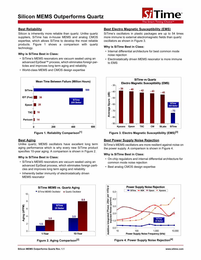
Best ReliabilitySilicon is inherently more reliable than quartz. Unlike quartzsuppliers, SiTime has in-house MEMS and analog CMOSexpertise, which allows SiTime to develop the most reliableproducts. Figure 1 shows a comparison with quartztechnology.
Why is SiTime Best in Class:
• SiTime’s MEMS resonators are vacuum sealed using an advanced EpiSeal™ process, which eliminates foreign par-ticles and improves long term aging and reliability
• World-class MEMS and CMOS design expertise
Figure 1. Reliability Comparison[1]
Best AgingUnlike quartz, MEMS oscillators have excellent long termaging performance which is why every new SiTime productspecifies 10-year aging. A comparison is shown in Figure 2.
Why is SiTime Best in Class:
• SiTime’s MEMS resonators are vacuum sealed using an advanced EpiSeal process, which eliminates foreign parti-cles and improves long term aging and reliability
• Inherently better immunity of electrostatically driven MEMS resonator
Figure 2. Aging Comparison[2]
Best Electro Magnetic Susceptibility (EMS)SiTime’s oscillators in plastic packages are up to 54 timesmore immune to external electromagnetic fields than quartz oscillators as shown in Figure 3.
Why is SiTime Best in Class:
• Internal differential architecture for best common mode noise rejection
• Electrostatically driven MEMS resonator is more immune to EMS
Figure 3. Electro Magnetic Susceptibility (EMS)[3]
Best Power Supply Noise RejectionSiTime’s MEMS oscillators are more resilient against noise onthe power supply. A comparison is shown in Figure 4.
Why is SiTime Best in Class:
• On-chip regulators and internal differential architecture for common mode noise rejection
• Best analog CMOS design expertise
Figure 4. Power Supply Noise Rejection[4]
Mean Time Between Failure (Million Hours)
14
16
28
38
500
0 200 400 600
Pericom
TXC
Epson
IDT (Fox)
SiTime
SiTime20X Better
1.5
3.53.0
8.0
0
2
4
6
8
10
1-Year 10-Year
SiTime MEMS vs. Quartz AgingSiTime MEMS Oscillator Quartz Oscillator
Ag
ing
(±P
PM
) SiTime 2X Better
- 39 - 40 - 42 - 43 - 45
- 73
- 90
- 80
- 70
- 60
- 50
- 40
- 30
Kyocera Epson TXC CW SiLabs SiTime
SiTime vs Quartz Electro Magnetic Susceptibility (EMS)
Ave
rag
e S
pu
rs
(dB
)
SiTime54X Better
0.0
1.0
2.0
3.0
4.0
5.0
10 100 1,000 10,000
Ad
dit
ive
Inte
gra
ted
Ph
ase
Jit
ter
per
mV
p-p
Inje
cte
d N
ois
e (
ps
/mv
)
Power Supply Noise Frequency (kHz)
Power Supply Noise RejectionSiTIme NDK Epson Kyocera
SiTime SiTime3X Better

The Smart Timing ChoiceThe Smart Timing Choice
Silicon MEMS Outperforms Quartz
Silicon MEMS Outperforms Quartz Rev. 1.1 www.sitime.com
Best Vibration Robustness
High-vibration environments are all around us. All electronics,from handheld devices to enterprise servers and storagesystems are subject to vibration. Figure 5 shows a comparisonof vibration robustness.
Why is SiTime Best in Class:
• The moving mass of SiTime’s MEMS resonators is up to 3000 times smaller than quartz
• Center-anchored MEMS resonator is the most robust design
Figure 5. Vibration Robustness[5]
Best Shock RobustnessSiTime’s oscillators can withstand at least 50,000 g shock.They all maintain their electrical performance in operationduring shock events. A comparison with quartz devices isshown in Figure 6.
Why is SiTime Best in Class:
• The moving mass of SiTime’s MEMS resonators is up to 3000 times smaller than quartz
• Center-anchored MEMS resonator is the most robust design
Figure 6. Shock Robustness[6]
Vib
rati
on
Sen
siti
vity
(p
pb
/g)
0.10
1.00
10.00
100.00
10 100 1000Vibration Frequency (Hz)
Vibration Sensitivity vs. FrequencySiTime TXC Epson Connor Winfield Kyocera SiLabs
SiTimeUp to 30x
Better
14.3
12.6
3.92.9 2.5
0.6
0
2
4
6
8
10
12
14
16
Kyocera Epson TXC CW SiLabs SiTime
Differential XO Shock Robustness - 500 g
SiTimeUp to 25x
Better P
eak
Fre
qu
ency
De
via
tio
n (
PP
M)
Notes:
1. Data Source: Reliability documents of named companies.
2. Data source: SiTime and quartz oscillator devices datasheets.
3. Test conditions for Electro Magnetic Susceptibility (EMS):
• According to IEC EN61000-4.3 (Electromagnetic compatibility standard)
• Field strength: 3V/m
• Radiated signal modulation: AM 1 kHz at 80% depth
• Carrier frequency scan: 80 MHz – 1 GHz in 1% steps
• Antenna polarization: Vertical
• DUT position: Center aligned to antenna
Devices used in this test:
SiTime, SiT9120AC-1D2-33E156.250000 - MEMS based - 156.25 MHz
Epson, EG-2102CA 156.2500M-PHPAL3 - SAW based - 156.25 MHz
TXC, BB-156.250MBE-T - 3rd Overtone quartz based - 156.25 MHz
Kyocera, KC7050T156.250P30E00 - SAW based - 156.25 MHz
Connor Winfield (CW), P123-156.25M - 3rd overtone quartz based - 156.25 MHz
SiLabs, Si590AB-BDG - 3rd overtone quartz based - 156.25 MHz
4. 50 mV pk-pk Sinusoidal voltage.
Devices used in this test:
SiTime, SiT8208AI-33-33E-25.000000, MEMS based - 25 MHz
NDK, NZ2523SB-25.6M - quartz based - 25.6 MHz
Kyocera, KC2016B25M0C1GE00 - quartz based - 25 MHz
Epson, SG-310SCF-25M0-MB3 - quartz based - 25 MHz
5. Devices used in this test: same as EMS test stated in Note 3.
6. Test conditions for shock test:
• MIL-STD-883F Method 2002
• Condition A: half sine wave shock pulse, 500-g, 1ms
• Continuous frequency measurement in 100 μs gate time for 10 seconds
Devices used in this test: same as EMS test stated in Note 3
7. Additional data, including setup and detailed results, is available upon request to qualified customers. Please contact [email protected].

The Smart Timing ChoiceThe Smart Timing Choice
Document Feedback Form
Feedback Form Rev. 1.0 www.sitime.com
SiTime values your input in improving our documentation. Click here for our online feedback form or fill out and email the form below to [email protected].
1. Does the Electrical Characteristics table provide complete information? Yes No
If No, what parameters are missing?
_________________________________________________________________________________________________
2. Is the organization of this document easy to follow? Yes No
If “No,” please suggest improvements that we can make:
_________________________________________________________________________________________________
3. Is there any application specific information that you would like to see in this document? (Check all that apply)
EMI Termination recommendations Shock and vibration performance Other
If “Other,” please specify:
_________________________________________________________________________________________________
4. Are there any errors in this document? Yes No
If “Yes”, please specify (what and where):
_________________________________________________________________________________________________
5. Do you have additional recommendations for this document?
_________________________________________________________________________________________________
Name ________________________________________________________________________________
Title ________________________________________________________________________________
Company _________________________________________________________________________________________
Address _________________________________________________________________________________________
City / State or Province / Postal Code / Country ___________________________________________________________
Telephone __________________________________
Application ________________________________________________________________________________________
Would you like a reply? Yes No
Thank you for your feedback. Please click the email icon in your Adobe Reader tool bar and send to [email protected] you may use our online feedback form.