Embed Size (px)
Citation preview
Struck Documentation SIS8300-L2MTCA.4 Digitizer
Page 1 of 85
SIS8300-L210 channel
125 MSPS 16-bitMTCA.4 Digitizer
User Manual
SIS GmbHHarksheider Str. 102A22399 HamburgGermany
Phone: ++49 (0) 40 60 87 305 0Fax: ++49 (0) 40 60 87 305 20
email: [email protected]://www.struck.de
Version: SIS8300L2-M-x009-1-V101.doc as of 03.07.2015
Struck Documentation SIS8300-L2µTCA 16-bit Digitizer
Page 2 of 85
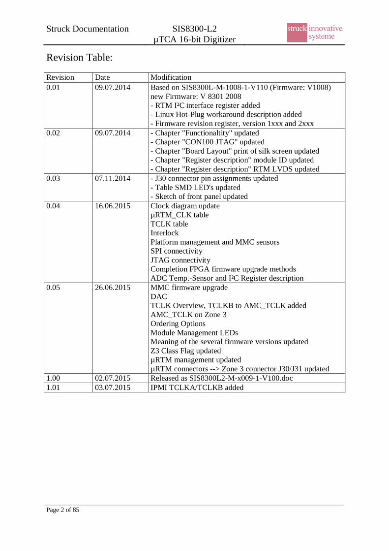
Revision Table:
Revision Date Modification0.01 09.07.2014 Based on SIS8300L-M-1008-1-V110 (Firmware: V1008)
new Firmware: V 8301 2008- RTM I²C interface register added- Linux Hot-Plug workaround description added- Firmware revision register, version 1xxx and 2xxx
0.02 09.07.2014 - Chapter "Functionaltity" updated- Chapter "CON100 JTAG" updated- Chapter "Board Layout" print of silk screen updated- Chapter "Register description" module ID updated- Chapter "Register description" RTM LVDS updated
0.03 07.11.2014 - J30 connector pin assignments updated- Table SMD LED's updated- Sketch of front panel updated
0.04 16.06.2015 Clock diagram updateµRTM_CLK tableTCLK tableInterlockPlatform management and MMC sensorsSPI connectivityJTAG connectivityCompletion FPGA firmware upgrade methodsADC Temp.-Sensor and I²C Register description
0.05 26.06.2015 MMC firmware upgradeDACTCLK Overview, TCLKB to AMC_TCLK addedAMC_TCLK on Zone 3Ordering OptionsModule Management LEDsMeaning of the several firmware versions updatedZ3 Class Flag updatedµRTM management updatedµRTM connectors --> Zone 3 connector J30/J31 updated
1.00 02.07.2015 Released as SIS8300L2-M-x009-1-V100.doc1.01 03.07.2015 IPMI TCLKA/TCLKB added
Struck Documentation SIS8300-L2MTCA.4 Digitizer
Page 3 of 85
- Table of contents- Table of contents....................................................................................................................................... 31 Introduction .............................................................................................................................................. 5
1.1 Related documents............................................................................................................................. 52 Design ...................................................................................................................................................... 6
2.1 Functionality ..................................................................................................................................... 62.2 Block Diagram .................................................................................................................................. 62.3 Platform Management........................................................................................................................ 7
2.3.1 E-Keying ................................................................................................................................... 72.3.2 MMC sensors............................................................................................................................. 82.3.3 MMC firmware upgrade............................................................................................................. 8
2.4 SPI Connectivity................................................................................................................................ 92.5 JTAG Connectivity.......................................................................................................................... 102.6 ADC Temperature Sensors............................................................................................................... 102.7 DAC................................................................................................................................................ 112.8 Clock Distribution ........................................................................................................................... 12
2.8.1 Overall Clock Distribution ....................................................................................................... 122.8.2 DAC Clock .............................................................................................................................. 132.8.3 µRTM Clock Overview............................................................................................................ 132.8.4 TCLK Clock Overview ............................................................................................................ 132.8.5 AMC_TCLK on Zone 3 ........................................................................................................... 142.8.6 MGT Clock.............................................................................................................................. 15
3 Jumper/Connector Pin Assignments......................................................................................................... 163.1 CON100 JTAG................................................................................................................................ 163.2 J604 Watchdog Reset....................................................................................................................... 163.3 J32 AVR JTAG ............................................................................................................................... 173.4 J33 ATxmega128 Debug ................................................................................................................. 17
4 LEDs ...................................................................................................................................................... 184.1 Module Management LEDs ............................................................................................................. 184.2 Front Panel LEDs ............................................................................................................................ 184.3 SMD LEDs...................................................................................................................................... 19
5 Front panel.............................................................................................................................................. 205.1 Harlink LVDS In-/Outputs............................................................................................................... 215.2 SMA Clock Input ........................................................................................................................... 215.3 SFP Card Cage ................................................................................................................................ 21
6 Board Layout .......................................................................................................................................... 227 Firmware Description.............................................................................................................................. 23
7.1 ADC Sample Logic ......................................................................................................................... 237.2 Memory Interface ............................................................................................................................ 24
7.2.1 Memory Write Interface ........................................................................................................... 257.3 Memory buffer ................................................................................................................................ 267.4 Address Map ................................................................................................................................... 277.5 Register description ......................................................................................................................... 29
7.5.1 Module Id. and Firmware Revision register .............................................................................. 297.5.2 Serial Number register.............................................................................................................. 297.5.3 User Control/Status register..................................................................................................... 307.5.4 Firmware Options register ........................................................................................................ 317.5.5 ADC Temperature Sensor interface register .............................................................................. 327.5.6 ADC Acquisition Control/Status register ................................................................................. 337.5.7 ADC Sample Control register ................................................................................................... 347.5.8 MLVDS Input/Output Control register ..................................................................................... 357.5.9 Harlink Connector Input/Output Control register ...................................................................... 367.5.10 Link1 Data FIFO...................................................................................................................... 377.5.11 Link1 Control Register ............................................................................................................. 387.5.12 Link2 Data FIFO...................................................................................................................... 397.5.13 Link2 Control Register ............................................................................................................. 407.5.14 Clock Distribution Multiplexer control register ......................................................................... 41
Struck Documentation SIS8300-L2µTCA 16-bit Digitizer
Page 4 of 85
7.5.15 Clock Distribution AD9510 Serial Interface (SPI) interface register .......................................... 437.5.16 Clock Multiplier IC SI5326 SPI interface register .................................................................... 457.5.17 Clock Synthesizer IC Si5338A I²C interface register................................................................. 467.5.18 FPGA Boot SPI Flash interface ................................................................................................ 477.5.19 DAC Control register ............................................................................................................... 487.5.20 DAC Data register.................................................................................................................... 497.5.21 RTM I2C interface register....................................................................................................... 507.5.22 ADC Serial Interface (SPI) interface register ............................................................................ 517.5.23 ADC Input Tap delay registers ................................................................................................. 527.5.24 Trigger registers....................................................................................................................... 537.5.25 Memory Sample Start Block Address / Actual Sample Block Address registers......................... 567.5.26 Sample Block Length register................................................................................................... 577.5.27 Ringbuffer Delay register ......................................................................................................... 577.5.28 SIS8900 RTM LVDS Test Input/Output Control register .......................................................... 587.5.29 Read DMA System Destination address (lower 32bits) ............................................................. 607.5.30 Read DMA System Destination address (upper 32bits) ............................................................. 607.5.31 Read DMA Card Memory Source address ................................................................................ 607.5.32 Read DMA Transfer length ...................................................................................................... 617.5.33 Read DMA Control.................................................................................................................. 617.5.34 Readout DMA Sample byte swap ............................................................................................. 627.5.35 Write DMA System Source address (lower 32bits) ................................................................... 637.5.36 Write DMA System Source address (upper 32bits) ................................................................... 637.5.37 Write DMA Card Memory Destination address......................................................................... 637.5.38 Write DMA Transfer length ..................................................................................................... 647.5.39 Write DMA Control ................................................................................................................. 647.5.40 DAQ Done DMA Chain Control .............................................................................................. 657.5.41 IRQ Enable.............................................................................................................................. 657.5.42 IRQ Status ............................................................................................................................... 667.5.43 IRQ Clear ................................................................................................................................ 667.5.44 IRQ Refresh............................................................................................................................. 667.5.45 RAM FIFO debug register........................................................................................................ 67
7.6 External register interface ................................................................................................................ 687.7 User Blockram DMA Interface ........................................................................................................ 707.8 User Interrupt Interface.................................................................................................................... 70
8 µRTM management ................................................................................................................................ 719 FPGA Firmware upgrade......................................................................................................................... 72
9.1 Create Bit/Bin files .......................................................................................................................... 729.2 iMPACT ......................................................................................................................................... 739.3 Linux tool ‘flashupdater’ ................................................................................................................. 759.4 Linux tool ‘ipmitool’ ....................................................................................................................... 759.5 Linux workaround for PCIe-Hot-Plug .............................................................................................. 75
10 Appendix ............................................................................................................................................ 7610.1 Power Consumption......................................................................................................................... 7610.2 Ordering options.............................................................................................................................. 7610.3 Zone 3 connectors J30 and J31......................................................................................................... 77
10.3.1 J31 connector pin assignments.................................................................................................. 7710.3.2 J30 connector pin assignments.................................................................................................. 7710.3.3 Note on AC/DC input stage selection........................................................................................ 7910.3.4 Interlock .................................................................................................................................. 81
10.4 Zone 3 connector schematic............................................................................................................. 8210.5 MMC Readme file........................................................................................................................... 83
11 Index................................................................................................................................................... 84
Struck Documentation SIS8300-L2MTCA.4 Digitizer
Page 5 of 85
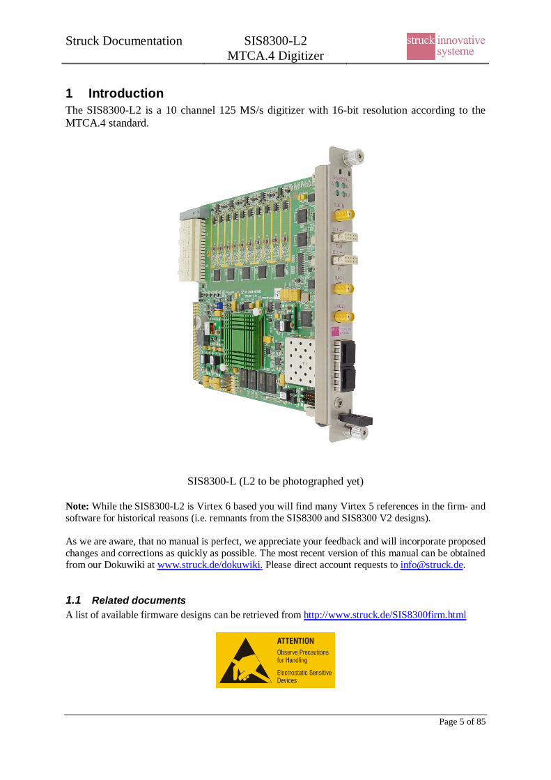
1 IntroductionThe SIS8300-L2 is a 10 channel 125 MS/s digitizer with 16-bit resolution according to theMTCA.4 standard.
SIS8300-L (L2 to be photographed yet)
Note: While the SIS8300-L2 is Virtex 6 based you will find many Virtex 5 references in the firm- andsoftware for historical reasons (i.e. remnants from the SIS8300 and SIS8300 V2 designs).
As we are aware, that no manual is perfect, we appreciate your feedback and will incorporate proposedchanges and corrections as quickly as possible. The most recent version of this manual can be obtainedfrom our Dokuwiki at www.struck.de/dokuwiki. Please direct account requests to [email protected].
1.1 Related documentsA list of available firmware designs can be retrieved from http://www.struck.de/SIS8300firm.html
Struck Documentation SIS8300-L2MTCA.4 Digitizer
Page 6 of 85
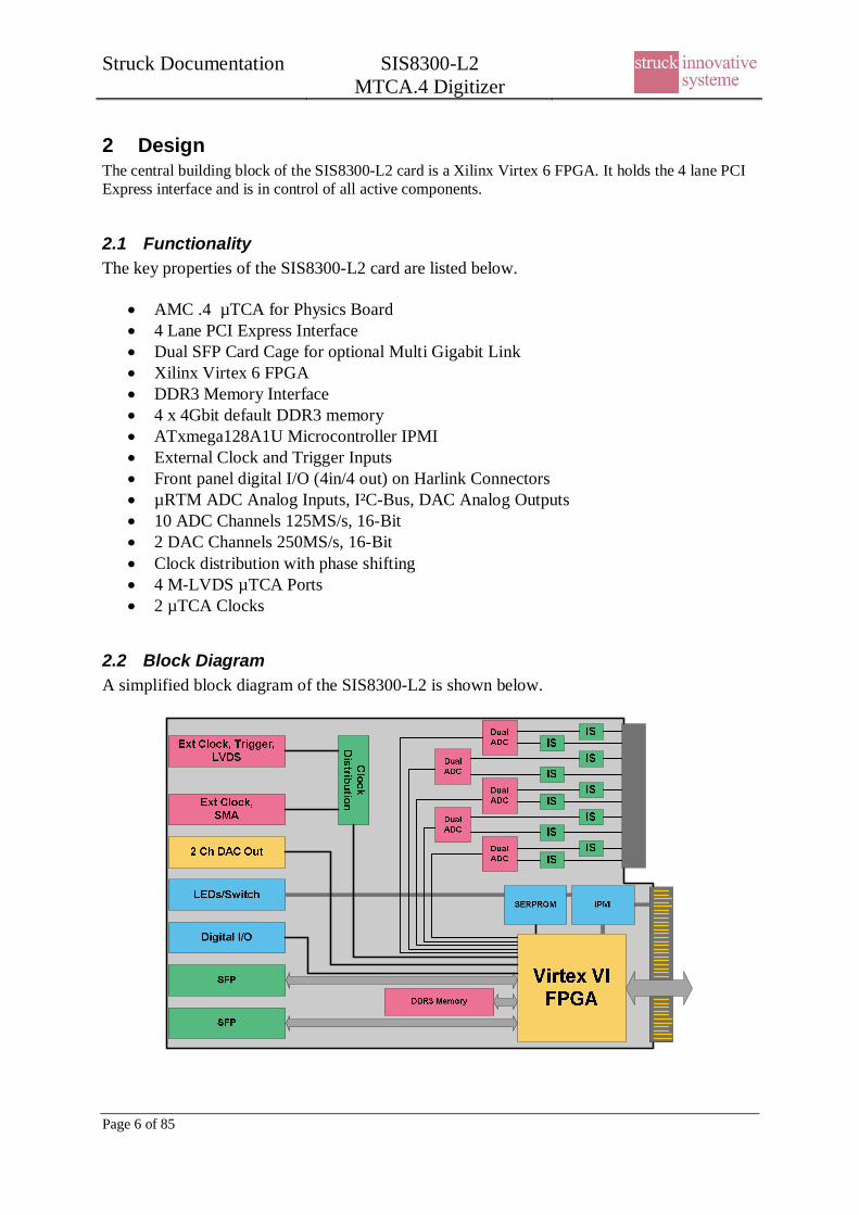
2 DesignThe central building block of the SIS8300-L2 card is a Xilinx Virtex 6 FPGA. It holds the 4 lane PCIExpress interface and is in control of all active components.
2.1 FunctionalityThe key properties of the SIS8300-L2 card are listed below.
AMC .4 µTCA for Physics Board4 Lane PCI Express InterfaceDual SFP Card Cage for optional Multi Gigabit LinkXilinx Virtex 6 FPGADDR3 Memory Interface4 x 4Gbit default DDR3 memoryATxmega128A1U Microcontroller IPMIExternal Clock and Trigger InputsFront panel digital I/O (4in/4 out) on Harlink ConnectorsµRTM ADC Analog Inputs, I²C-Bus, DAC Analog Outputs10 ADC Channels 125MS/s, 16-Bit2 DAC Channels 250MS/s, 16-BitClock distribution with phase shifting4 M-LVDS µTCA Ports2 µTCA Clocks
2.2 Block DiagramA simplified block diagram of the SIS8300-L2 is shown below.
Struck Documentation SIS8300-L2MTCA.4 Digitizer
Page 7 of 85
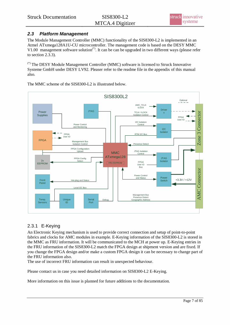
2.3 Platform ManagementThe Module Management Controller (MMC) functionality of the SIS8300-L2 is implemented in anAtmel ATxmega128A1U-CU microcontroller. The management code is based on the DESY MMCV1.00 management software solution(*). It can be can be upgraded in two different ways (please referto section 2.3.3).
(*) The DESY Module Management Controller (MMC) software is licensed to Struck InnovativeSysteme GmbH under DESY LV92. Pleaser refer to the readme file in the appendix of this manualalso.
The MMC scheme of the SIS8300-L2 is illustrated below.
Zone
3 C
onne
ctor
AM
C C
onne
ctor
FPGA
I2C IsolationControl
SIS8300L2
+3.3V / +12V
PowerSupplies
MMCATxmega128
FRU EEPROM
JTAG
FrontPanel
Temp.Sensors
UniqueID
SerialPort
PowerSwitch
I2CIsolator
Driverx
Power Controland Monitoring
Management BusIsolation Control
Hot-plug and Status
Local I2C Bus
Debug
Management BusPresence Detect
Geographic Address
TCLK / ILOCKIsolation Control
Power Controland Status
JTAGIsolator
Optional
AMC_TCLKILOCK
JTAG IsolationControl
FPGAUser IO
Bus
Presence Detect
2xEEPROM
FPGA ConfigurationUpload
FPGA ConfigSelect
RTM I2C Bus
FPGAUser IO
FPGAUser IO
2.3.1 E-KeyingAn Electronic Keying mechanism is used to provide correct connection and setup of point-to-pointfabrics and clocks for AMC modules in example. E-Keying information of the SIS8300-L2 is stored inthe MMC as FRU information. It will be communicated to the MCH at power up. E-Keying entries inthe FRU information of the SIS8300-L2 match the FPGA design at shipment version and are fixed. Ifyou change the FPGA design and/or make a custom FPGA design it can be necessary to change part ofthe FRU information also.The use of incorrect FRU information can result in unexpected behaviour.
Please contact us in case you need detailed information on SIS8300-L2 E-Keying.
More information on this issue is planned for future additions to the documentation.
Struck Documentation SIS8300-L2MTCA.4 Digitizer
Page 8 of 85
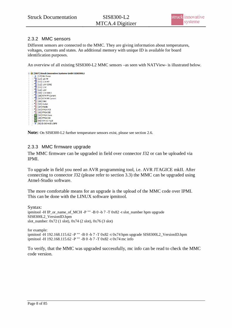
2.3.2 MMC sensorsDifferent sensors are connected to the MMC. They are giving information about temperatures,voltages, currents and states. An additional memory with unique ID is available for boardidentification purposes.
An overview of all existing SIS8300-L2 MMC sensors –as seen with NATView- is illustrated below.
Note: On SIS8300-L2 further temperature sensors exist, please see section 2.6.
2.3.3 MMC firmware upgradeThe MMC firmware can be upgraded in field over connector J32 or can be uploaded viaIPMI.
To upgrade in field you need an AVR programming tool, i.e. AVR JTAGICE mkII. Afterconnecting to connector J32 (please refer to section 3.3) the MMC can be upgraded usingAtmel-Studio software.
The more comfortable means for an upgrade is the upload of the MMC code over IPMI.This can be done with the LINUX software ipmitool.
Syntax:ipmitool -H IP_or_name_of_MCH -P "" -B 0 -b 7 -T 0x82 -t slot_number hpm upgradeSIS8300L2_VersionID.hpmslot_number: 0x72 (1 slot), 0x74 (2 slot), 0x76 (3 slot)
for example:ipmitool -H 192.168.115.62 -P "" -B 0 -b 7 -T 0x82 -t 0x74 hpm upgrade SIS8300L2_VersionID.hpmipmitool -H 192.168.115.62 -P "" -B 0 -b 7 -T 0x82 -t 0x74 mc info
To verify, that the MMC was upgraded successfully, mc info can be read to check the MMCcode version.
Struck Documentation SIS8300-L2MTCA.4 Digitizer
Page 9 of 85
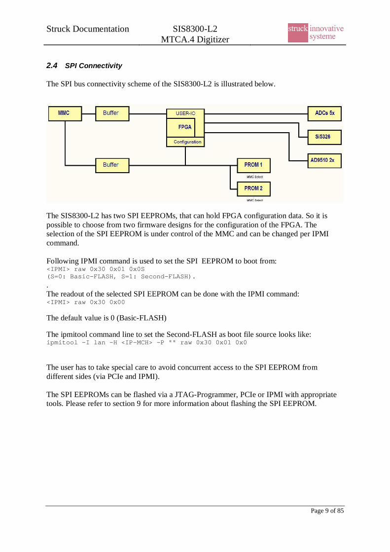
2.4 SPI Connectivity
The SPI bus connectivity scheme of the SIS8300-L2 is illustrated below.
The SIS8300-L2 has two SPI EEPROMs, that can hold FPGA configuration data. So it ispossible to choose from two firmware designs for the configuration of the FPGA. Theselection of the SPI EEPROM is under control of the MMC and can be changed per IPMIcommand.
Following IPMI command is used to set the SPI EEPROM to boot from:<IPMI> raw 0x30 0x01 0x0S(S=0: Basic-FLASH, S=1: Second-FLASH)..The readout of the selected SPI EEPROM can be done with the IPMI command:<IPMI> raw 0x30 0x00
The default value is 0 (Basic-FLASH)
The ipmitool command line to set the Second-FLASH as boot file source looks like:ipmitool -I lan -H <IP-MCH> -P "" raw 0x30 0x01 0x0
The user has to take special care to avoid concurrent access to the SPI EEPROM fromdifferent sides (via PCIe and IPMI).
The SPI EEPROMs can be flashed via a JTAG-Programmer, PCIe or IPMI with appropriatetools. Please refer to section 9 for more information about flashing the SPI EEPROM.

Struck Documentation SIS8300-L2MTCA.4 Digitizer
Page 10 of 85
2.5 JTAG Connectivity
The JTAG connectivity scheme of the SIS8300-L2 is illustrated below.
JTAG connection to µRTM can be realized in FPGA firmware but is a optional feature forfuture.Switching connection of FPGA hardware JTAG port between MTCA (AMC Backplane) andon board JTAG connector (illustrated switch CON/MTCA) can be made via IPMI command.
IPMI command ... (not implemented yet, please request us for more information)
Upon power up the switch CON/MTCA connects the JTAG connector to the JTAG port ofthe FPGA hardware.
2.6 ADC Temperature Sensors
Two thermistor based sensors are used to measure the temperature at the beginning and theend of the row of the 5 digitizer chips.
The location of both sensors on the bottom side as seen from the top is shown below.
Struck Documentation SIS8300-L2MTCA.4 Digitizer
Page 11 of 85
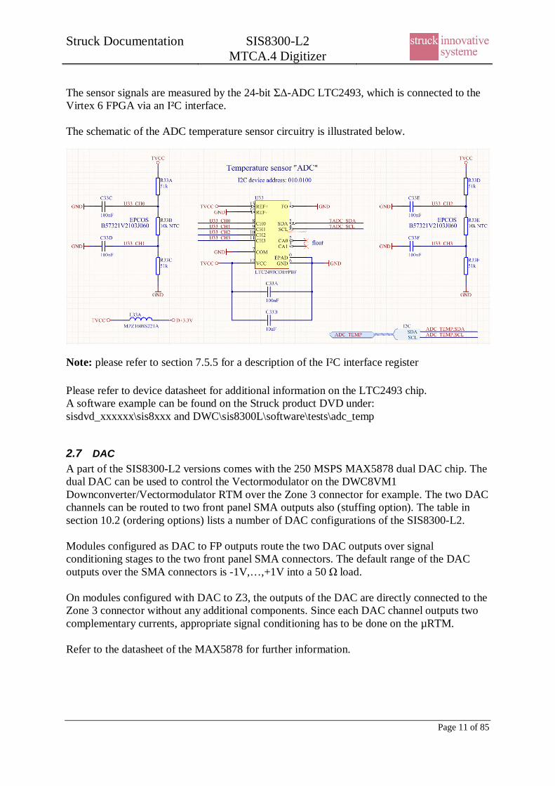
The sensor signals are measured by the 24-bit -ADC LTC2493, which is connected to theVirtex 6 FPGA via an I²C interface.
The schematic of the ADC temperature sensor circuitry is illustrated below.
Note: please refer to section 7.5.5 for a description of the I²C interface register
Please refer to device datasheet for additional information on the LTC2493 chip.A software example can be found on the Struck product DVD under:sisdvd_xxxxxx\sis8xxx and DWC\sis8300L\software\tests\adc_temp
2.7 DACA part of the SIS8300-L2 versions comes with the 250 MSPS MAX5878 dual DAC chip. Thedual DAC can be used to control the Vectormodulator on the DWC8VM1Downconverter/Vectormodulator RTM over the Zone 3 connector for example. The two DACchannels can be routed to two front panel SMA outputs also (stuffing option). The table insection 10.2 (ordering options) lists a number of DAC configurations of the SIS8300-L2.
Modules configured as DAC to FP outputs route the two DAC outputs over signalconditioning stages to the two front panel SMA connectors. The default range of the DACoutputs over the SMA connectors is -1V,…,+1V into a 50 load.
On modules configured with DAC to Z3, the outputs of the DAC are directly connected to theZone 3 connector without any additional components. Since each DAC channel outputs twocomplementary currents, appropriate signal conditioning has to be done on the µRTM.
Refer to the datasheet of the MAX5878 for further information.
Struck Documentation SIS8300-L2MTCA.4 Digitizer
Page 12 of 85
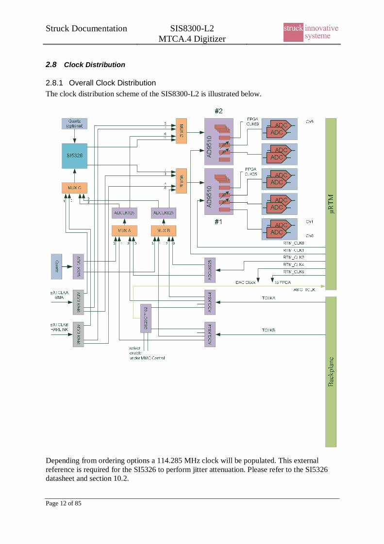
2.8 Clock Distribution
2.8.1 Overall Clock DistributionThe clock distribution scheme of the SIS8300-L2 is illustrated below.
Depending from ordering options a 114.285 MHz clock will be populated. This externalreference is required for the SI5326 to perform jitter attenuation. Please refer to the SI5326datasheet and section 10.2.
Struck Documentation SIS8300-L2MTCA.4 Digitizer
Page 13 of 85
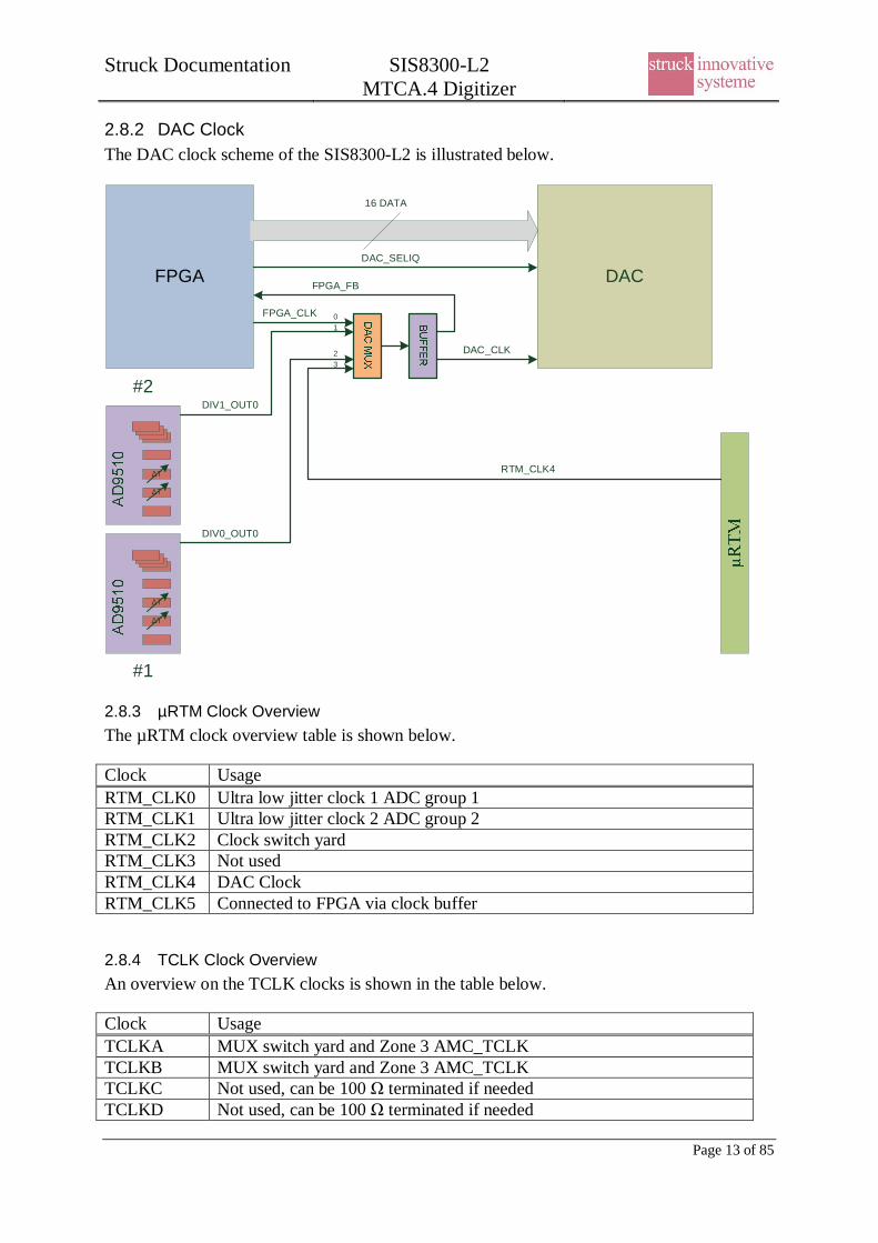
2.8.2 DAC ClockThe DAC clock scheme of the SIS8300-L2 is illustrated below.
FPGA DAC
01
T
T
#1
#2
T
T
23
RTM_CLK4
DIV0_OUT0
DIV1_OUT0
FPGA_FB
FPGA_CLK
DAC_CLK
16 DATA
DAC_SELIQ
2.8.3 µRTM Clock OverviewThe µRTM clock overview table is shown below.
Clock UsageRTM_CLK0 Ultra low jitter clock 1 ADC group 1RTM_CLK1 Ultra low jitter clock 2 ADC group 2RTM_CLK2 Clock switch yardRTM_CLK3 Not usedRTM_CLK4 DAC ClockRTM_CLK5 Connected to FPGA via clock buffer
2.8.4 TCLK Clock OverviewAn overview on the TCLK clocks is shown in the table below.
Clock UsageTCLKA MUX switch yard and Zone 3 AMC_TCLKTCLKB MUX switch yard and Zone 3 AMC_TCLKTCLKC Not used, can be 100 terminated if neededTCLKD Not used, can be 100 terminated if needed
Struck Documentation SIS8300-L2MTCA.4 Digitizer
Page 14 of 85
2.8.5 AMC_TCLK on Zone 3The AMC_TCLK signal can be derived from TCLKA or TCLKB. Selection and outputcontrol of AMC_TCLK switch is under control of MMC. Currently the state of both signalscan be read from SIS8900 RTM LVDS Test Input/Output Control register, please refer tosection 7.5.28.
The TCLKA or TCLKB selection can be made per IPMI command:
<IPMI> raw 0x30 0x03 0xEC(E=1/0: TCLK active/deactivated, C=0/1: select TCLKA/TCLKB)
The status can be read back with the command:
<IPMI> raw 0x30 0x02
After power up TCLKA is selected per default.
AMC_TCLK signals are available for SIS8300-L2 with Zone 3 class compatibility A1.1COand A1.0C only. Please refer to section 10.3.2.
Struck Documentation SIS8300-L2MTCA.4 Digitizer
Page 15 of 85
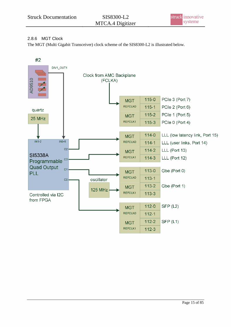
2.8.6 MGT ClockThe MGT (Multi Gigabit Transceiver) clock scheme of the SIS8300-L2 is illustrated below.
AD
9510
Struck Documentation SIS8300-L2MTCA.4 Digitizer
Page 16 of 85
3 Jumper/Connector Pin AssignmentsThe following subsections describe jumper and connector pin assignments.
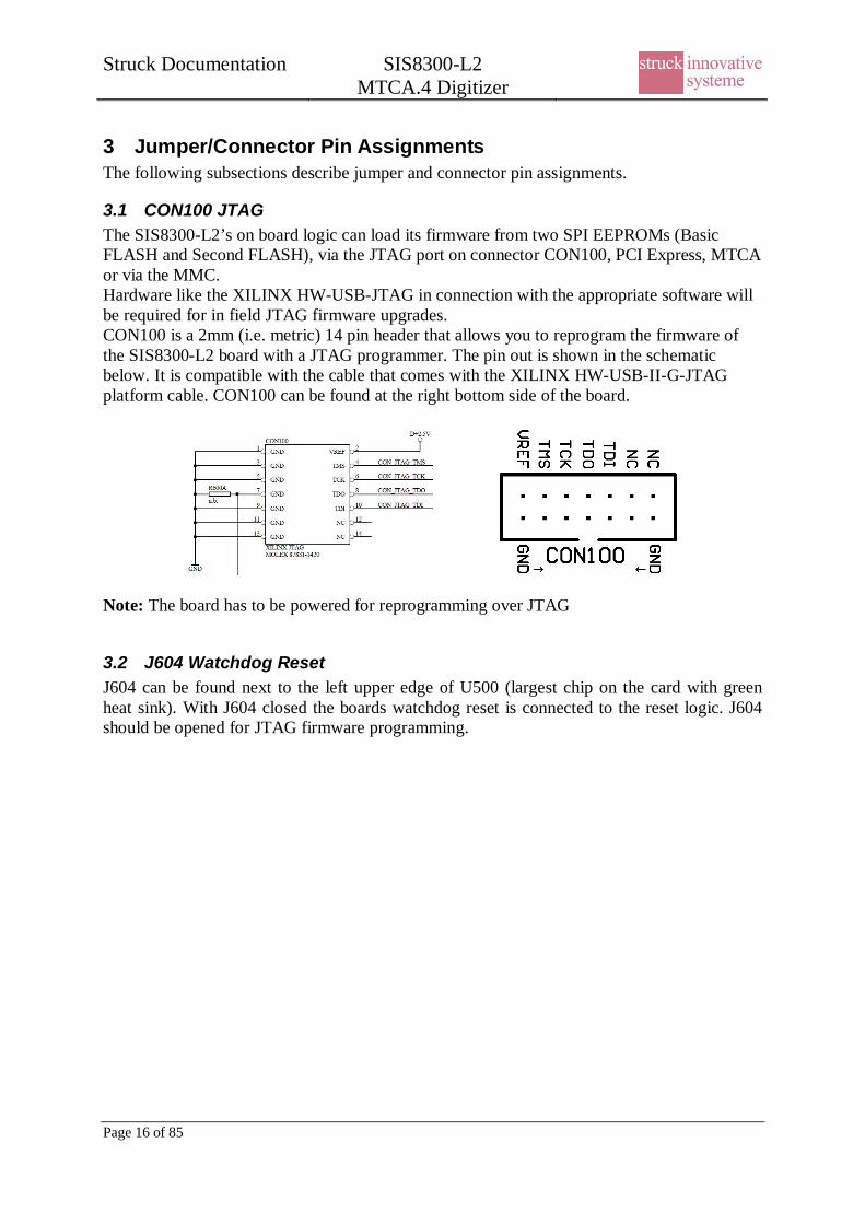
3.1 CON100 JTAGThe SIS8300-L2’s on board logic can load its firmware from two SPI EEPROMs (BasicFLASH and Second FLASH), via the JTAG port on connector CON100, PCI Express, MTCAor via the MMC.Hardware like the XILINX HW-USB-JTAG in connection with the appropriate software willbe required for in field JTAG firmware upgrades.CON100 is a 2mm (i.e. metric) 14 pin header that allows you to reprogram the firmware ofthe SIS8300-L2 board with a JTAG programmer. The pin out is shown in the schematicbelow. It is compatible with the cable that comes with the XILINX HW-USB-II-G-JTAGplatform cable. CON100 can be found at the right bottom side of the board.
Note: The board has to be powered for reprogramming over JTAG
3.2 J604 Watchdog ResetJ604 can be found next to the left upper edge of U500 (largest chip on the card with greenheat sink). With J604 closed the boards watchdog reset is connected to the reset logic. J604should be opened for JTAG firmware programming.
Struck Documentation SIS8300-L2MTCA.4 Digitizer
Page 17 of 85
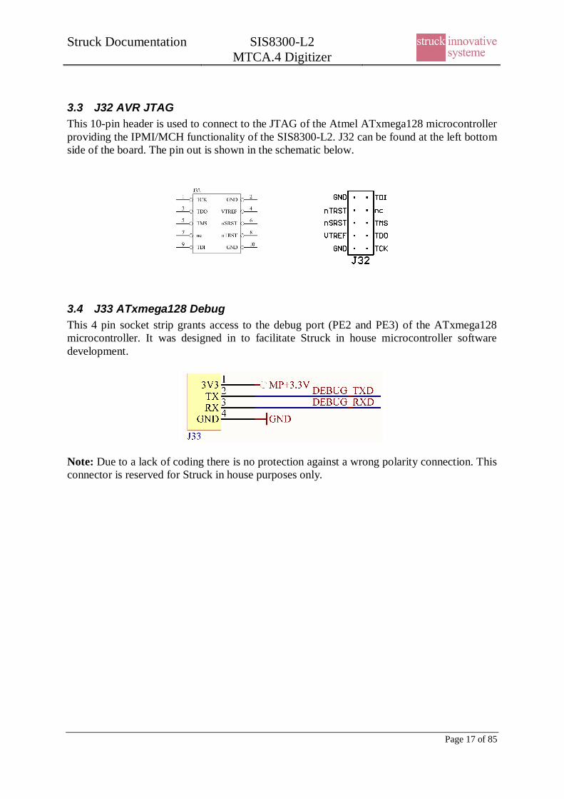
3.3 J32 AVR JTAGThis 10-pin header is used to connect to the JTAG of the Atmel ATxmega128 microcontrollerproviding the IPMI/MCH functionality of the SIS8300-L2. J32 can be found at the left bottomside of the board. The pin out is shown in the schematic below.
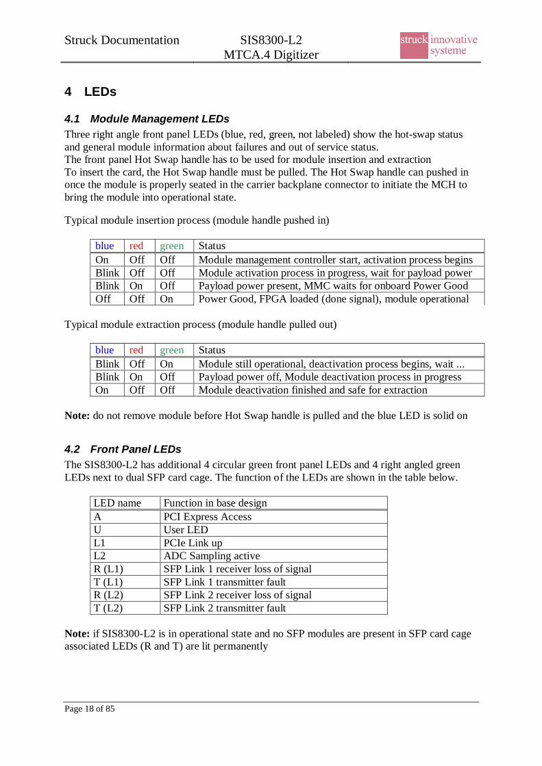
3.4 J33 ATxmega128 DebugThis 4 pin socket strip grants access to the debug port (PE2 and PE3) of the ATxmega128microcontroller. It was designed in to facilitate Struck in house microcontroller softwaredevelopment.
Note: Due to a lack of coding there is no protection against a wrong polarity connection. Thisconnector is reserved for Struck in house purposes only.
Struck Documentation SIS8300-L2MTCA.4 Digitizer
Page 18 of 85
4 LEDs
4.1 Module Management LEDsThree right angle front panel LEDs (blue, red, green, not labeled) show the hot-swap statusand general module information about failures and out of service status.The front panel Hot Swap handle has to be used for module insertion and extractionTo insert the card, the Hot Swap handle must be pulled. The Hot Swap handle can pushed inonce the module is properly seated in the carrier backplane connector to initiate the MCH tobring the module into operational state.
Typical module insertion process (module handle pushed in)
blue red green StatusOn Off Off Module management controller start, activation process beginsBlink Off Off Module activation process in progress, wait for payload powerBlink On Off Payload power present, MMC waits for onboard Power GoodOff Off On Power Good, FPGA loaded (done signal), module operational
Typical module extraction process (module handle pulled out)
blue red green StatusBlink Off On Module still operational, deactivation process begins, wait ...Blink On Off Payload power off, Module deactivation process in progressOn Off Off Module deactivation finished and safe for extraction
Note: do not remove module before Hot Swap handle is pulled and the blue LED is solid on
4.2 Front Panel LEDsThe SIS8300-L2 has additional 4 circular green front panel LEDs and 4 right angled greenLEDs next to dual SFP card cage. The function of the LEDs are shown in the table below.
LED name Function in base designA PCI Express AccessU User LEDL1 PCIe Link upL2 ADC Sampling activeR (L1) SFP Link 1 receiver loss of signalT (L1) SFP Link 1 transmitter faultR (L2) SFP Link 2 receiver loss of signalT (L2) SFP Link 2 transmitter fault
Note: if SIS8300-L2 is in operational state and no SFP modules are present in SFP card cageassociated LEDs (R and T) are lit permanently
Struck Documentation SIS8300-L2MTCA.4 Digitizer
Page 19 of 85
4.3 SMD LEDsA number of surface mount red LEDs are on the SIS8300-L2 to visualize part of the boardstatus.
LED designator LED comment FunctionD20A S1 Firmware dependent
(Optical Link 1 up)D20B S2 Firmware dependent
(Optical Link 2 up)D20C S3 Firmware dependentD20D S4 Firmware dependentD20E S5 Firmware dependentD20F S6 Firmware dependentD20G S7 Firmware dependentD20H S8 Firmware dependentD21D READY FPGA readyD10A +12V Payload power presentD10B MP+3.3V Management power present
Struck Documentation SIS8300-L2MTCA.4 Digitizer
Page 20 of 85
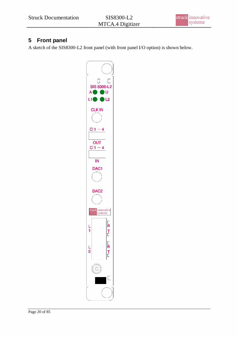
5 Front panelA sketch of the SIS8300-L2 front panel (with front panel I/O option) is shown below.
Struck Documentation SIS8300-L2MTCA.4 Digitizer
Page 21 of 85
5.1 Harlink LVDS In-/OutputsThe Harlink LVDS Output and Input connectors have 5 signals each. The Clock signal to theleft hand side is marked with C and the other 4 signals are labelled with 1-4.
Clock 1 2 3 4Top P P P P P
Bottom N N N N N
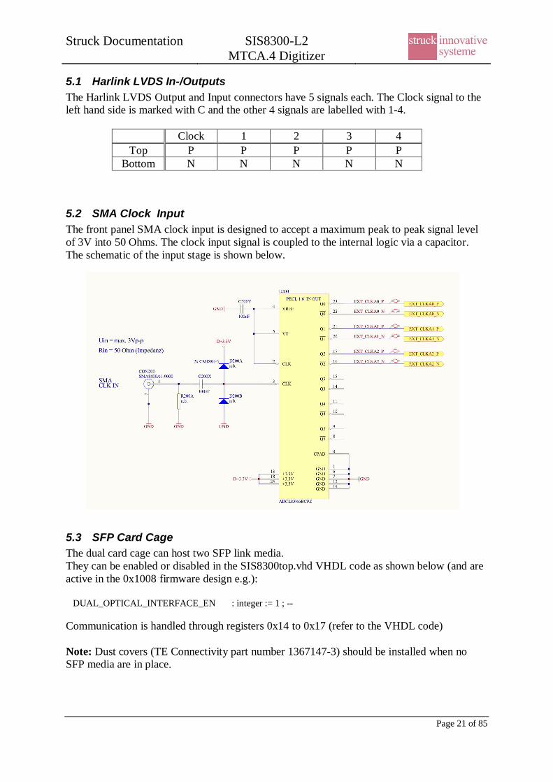
5.2 SMA Clock InputThe front panel SMA clock input is designed to accept a maximum peak to peak signal levelof 3V into 50 Ohms. The clock input signal is coupled to the internal logic via a capacitor.The schematic of the input stage is shown below.
5.3 SFP Card CageThe dual card cage can host two SFP link media.They can be enabled or disabled in the SIS8300top.vhd VHDL code as shown below (and areactive in the 0x1008 firmware design e.g.):
DUAL_OPTICAL_INTERFACE_EN : integer := 1 ; --
Communication is handled through registers 0x14 to 0x17 (refer to the VHDL code)
Note: Dust covers (TE Connectivity part number 1367147-3) should be installed when noSFP media are in place.
Struck Documentation SIS8300-L2MTCA.4 Digitizer
Page 22 of 85
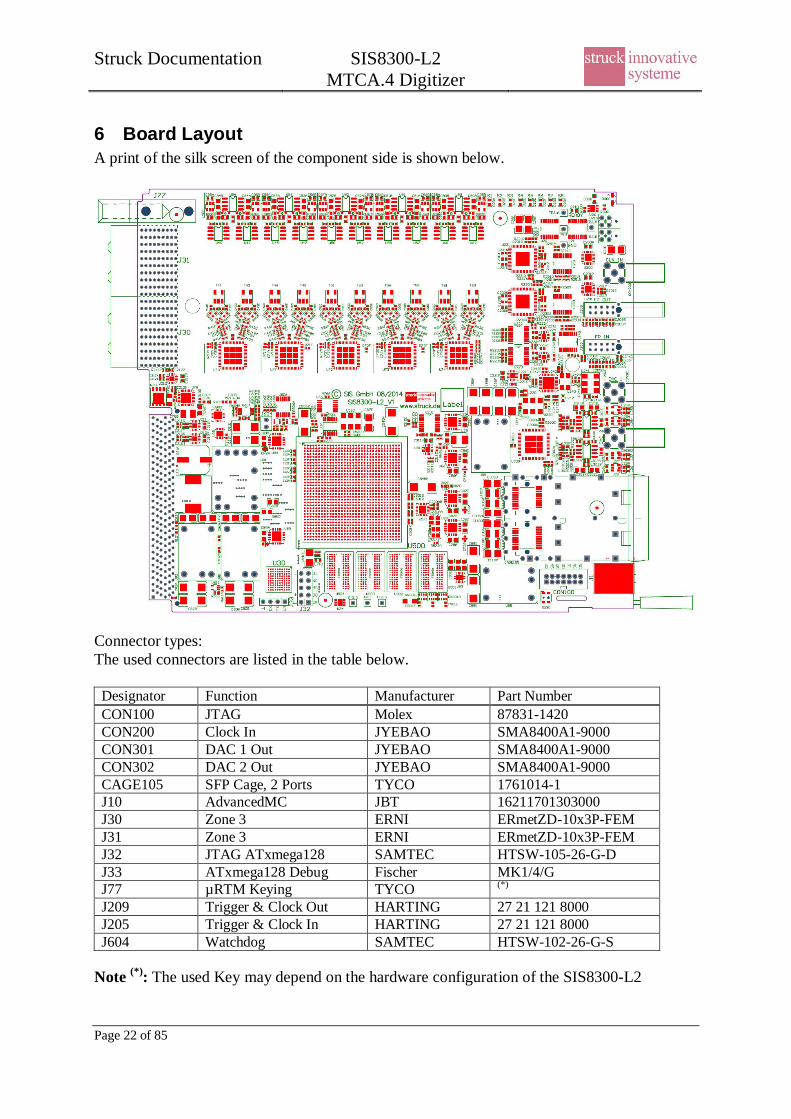
6 Board LayoutA print of the silk screen of the component side is shown below.
Connector types:The used connectors are listed in the table below.
Designator Function Manufacturer Part NumberCON100 JTAG Molex 87831-1420CON200 Clock In JYEBAO SMA8400A1-9000CON301 DAC 1 Out JYEBAO SMA8400A1-9000CON302 DAC 2 Out JYEBAO SMA8400A1-9000CAGE105 SFP Cage, 2 Ports TYCO 1761014-1J10 AdvancedMC JBT 16211701303000J30 Zone 3 ERNI ERmetZD-10x3P-FEMJ31 Zone 3 ERNI ERmetZD-10x3P-FEMJ32 JTAG ATxmega128 SAMTEC HTSW-105-26-G-DJ33 ATxmega128 Debug Fischer MK1/4/GJ77 µRTM Keying TYCO (*)
J209 Trigger & Clock Out HARTING 27 21 121 8000J205 Trigger & Clock In HARTING 27 21 121 8000J604 Watchdog SAMTEC HTSW-102-26-G-S
Note (*): The used Key may depend on the hardware configuration of the SIS8300-L2

Struck Documentation SIS8300-L2MTCA.4 Digitizer
Page 23 of 85
7 Firmware Description
7.1 ADC Sample Logic
The block diagram shows the ADC data handling. Each ADC channel has its own Memory Address ControlLogic.
Struck Documentation SIS8300-L2MTCA.4 Digitizer
Page 24 of 85
7.2 Memory Interface
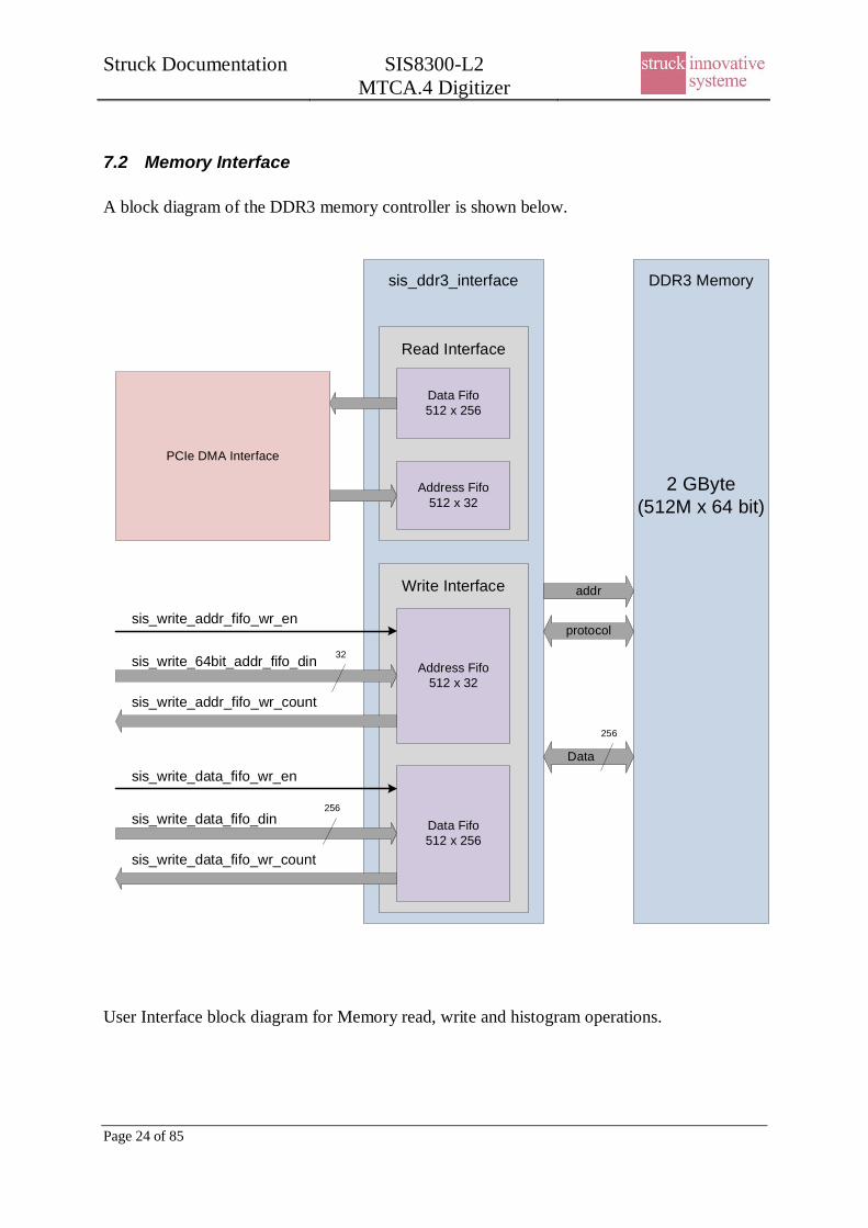
A block diagram of the DDR3 memory controller is shown below.
sis_ddr3_interface
Address Fifo512 x 32
sis_write_addr_fifo_wr_en
sis_write_64bit_addr_fifo_din
sis_write_addr_fifo_wr_count
Data Fifo512 x 256
sis_write_data_fifo_wr_en
sis_write_data_fifo_din
sis_write_data_fifo_wr_count
Write Interface
DDR3 Memory
Data
addr
protocol
2 GByte(512M x 64 bit)
Address Fifo512 x 32
Data Fifo512 x 256
Read Interface
PCIe DMA Interface
256
256
32
User Interface block diagram for Memory read, write and histogram operations.
Struck Documentation SIS8300-L2MTCA.4 Digitizer
Page 25 of 85
7.2.1 Memory Write Interface
The Write Interface consists of the following signals:
write_fifo_wr_clk : in std_logic;-- data: write fifowrite_data_fifo_wr_en : in std_logic;write_data_fifo_din : in std_logic_vector(255 downto 0);write_data_fifo_wr_count : out std_logic_vector(9 downto 0);
-- address: write fifowrite_addr_fifo_wr_en : in std_logic;write_addr_fifo_din : in std_logic_vector(31 downto 0);write_addr_fifo_wr_count : out std_logic_vector(9 downto 0);
A write cycle to the memory consists of one write command to the Address Fifo and onewrite commands to the Data Fifo.
One write command to the Address FIFO:a valid “sis_write_addr_fifo_wr_en” signal over one clock period(sis_write_fifo_wr_clk) along with “sis_write_64bit_addr_fifo_din”.
One write commands to the Data FIFO:a valid “sis_write_data_fifo_wr_en” signal over one clock periods(sis_write_fifo_wr_clk) along with “sis_write_data_fifo_din”.
When issuing a write command to the Address Fifo, the write command to the Data Fifo mustbe issued no more than zero clock cycle later.
It is only allowed to write to the Address-FIFO, if “sis_write_addr_fifo_wr_count” islower than X”1FF” (not full).It is only allowed to write to the Data-FIFO, if “sis_write_data_fifo_wr_count” is lowerthan X”1FE” (not full).
The Memory Controller writes 256 bits (4 x 64 bits) to memory with one “write cycle”.Therefore the lower 2 address bits of the written 64-bit address must be 0 and the “nextaddress” will be incremented by 4.
Struck Documentation SIS8300-L2MTCA.4 Digitizer
Page 26 of 85
7.3 Memory bufferThe structure of the memory buffer with 2 GByte (i.e. 4 x 4 GBit memory chips) is illustratedbelow.
Struck Documentation SIS8300-L2MTCA.4 Digitizer
Page 27 of 85
7.4 Address MapFollowing 32-bit addresses are implemented
Offset Access Function0x00 R Module Identifier/Firmware Version register0x01 R Serial number register0x02 R/W reserved0x03 R/W reserved
0x04 R/W User Control/Status register (JK)0x05 R Firmware Options register0x06 R/W ADC Temperature Sensor interface register
0x10 R/W ADC Acquisition Control/Status register0x11 R/W ADC Sample Control register0x12 R/W MLVDS Input/Output Control register0x13 R/W Harlink Connector Input/Output Control register
0x14 R/W Link 1 data FIFO (refer to VHDL code)0x15 R/W Link 1 set control (refer to VHDL code)0x16 R/W Link 2 data FIFO (refer to VHDL code)0x17 R/W Link 2 set control (refer to VHDL code)
0x40 R/W Clock Distribution Multiplexer control register0x41 R/W Clock Distribution IC AD9510 SPI interface register0x42 R/W Clock Multiplier IC SI5326 SPI interface register0x43 R/W Clock Synthesizer Si5338A for MGT clocks0x44 R/W FPGA Boot SPI Flash interface0x45 R/W DAC Control register0x46 R/W DAC Data register0x47 R/W RTM I2C interface register
0x48 R/W ADC SPI Interface register0x49 R/W ADC Input Tap delay register
0xFF W Bit 0 = 1: Master Reset (reset all registers)
Struck Documentation SIS8300-L2MTCA.4 Digitizer
Page 28 of 85
Offset Access Function0x100 R/W ADC ch1 Trigger Setup register0x101 R/W ADC ch2 Trigger Setup register .. .. .. ..0x109 R/W ADC ch10 Trigger Setup register
0x110 R/W ADC ch1 Trigger Threshold register0x111 R/W ADC ch2 Trigger Threshold register .. ..0x119 R/W ADC ch10 Trigger Threshold register
0x120 R/W ADC ch1 Memory Sample Start Block Address / Actual Block Address register0x121 R/W ADC ch2 Memory Sample Start Block Address / Actual Block Address register.. ..0x129 R/W ADC ch10 Memory Sample Start Block Address / Actual Block Address register
0x12A R/W ADC chx Sample Block Length register0x12B R/W ADC chx Ringbuffer Delay register (0 to 2046)
0x12F R/W SIS8900 RTM LVDS Test Input/Output Control register
0x200 R/W DMA_READ_DST_ADR_LO320x201 R/W DMA_READ_DST_ADR_HI320x202 R/W DMA_READ_SRC_ADR_LO320x203 R/W DMA_READ_LEN0x204 R/W DMA_READ_CTRL0x205 R/W DMA Readout Sample byte swap control
0x210 R/W DMA_WRITE_SRC_ADR_LO320x211 R/W DMA_WRITE_SRC_ADR_HI320x212 R/W DMA_WRITE_DST_ADR_LO320x213 R/W DMA_WRITE_LEN0x214 R/W DMA_WRITE_CTRL0x216 R/W DAQ Auto DMA Chain Control
0x220 R/W IRQ Enable0x221 R IRQ Status0x222 W IRQ Clear0x223 KA IRQ Refresh
0x230 R/W MEMORY test Mode register0x231 R/W RAM FIFO debug register
0x400 R/W Mapped out of register bank to top level. May be used for user defined registerimplementation. See Section 7.6.
...
...0x4FF R/W
Struck Documentation SIS8300-L2MTCA.4 Digitizer
Page 29 of 85
7.5 Register description
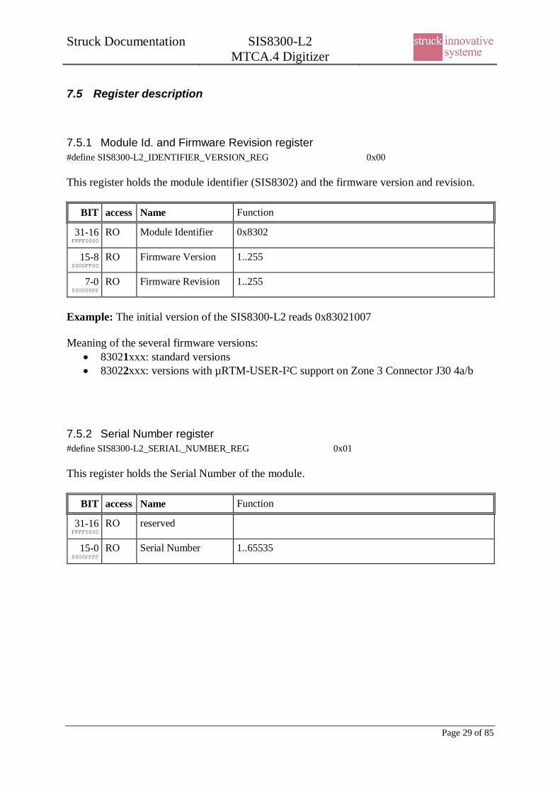
7.5.1 Module Id. and Firmware Revision register#define SIS8300-L2_IDENTIFIER_VERSION_REG 0x00
This register holds the module identifier (SIS8302) and the firmware version and revision.
BIT access Name Function
31-16FFFF0000
RO Module Identifier 0x8302
15-80000FF00
RO Firmware Version 1..255
7-0000000FF
RO Firmware Revision 1..255
Example: The initial version of the SIS8300-L2 reads 0x83021007
Meaning of the several firmware versions:83021xxx: standard versions83022xxx: versions with µRTM-USER-I²C support on Zone 3 Connector J30 4a/b
7.5.2 Serial Number register#define SIS8300-L2_SERIAL_NUMBER_REG 0x01
This register holds the Serial Number of the module.
BIT access Name Function
31-16FFFF0000
RO reserved
15-00000FFFF
RO Serial Number 1..65535
Struck Documentation SIS8300-L2MTCA.4 Digitizer
Page 30 of 85
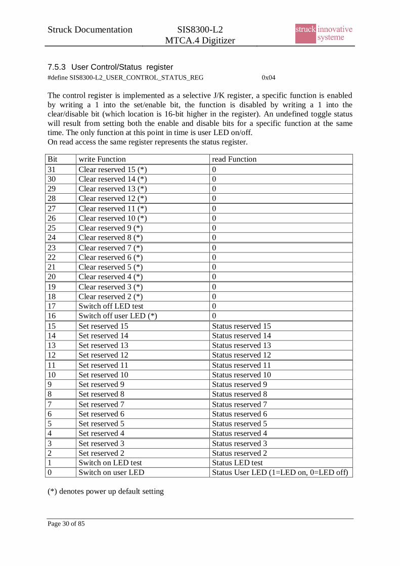
7.5.3 User Control/Status register#define SIS8300-L2_USER_CONTROL_STATUS_REG 0x04
The control register is implemented as a selective J/K register, a specific function is enabledby writing a 1 into the set/enable bit, the function is disabled by writing a 1 into theclear/disable bit (which location is 16-bit higher in the register). An undefined toggle statuswill result from setting both the enable and disable bits for a specific function at the sametime. The only function at this point in time is user LED on/off.On read access the same register represents the status register.
Bit write Function read Function31 Clear reserved 15 (*) 030 Clear reserved 14 (*) 029 Clear reserved 13 (*) 028 Clear reserved 12 (*) 027 Clear reserved 11 (*) 026 Clear reserved 10 (*) 025 Clear reserved 9 (*) 024 Clear reserved 8 (*) 023 Clear reserved 7 (*) 022 Clear reserved 6 (*) 021 Clear reserved 5 (*) 020 Clear reserved 4 (*) 019 Clear reserved 3 (*) 018 Clear reserved 2 (*) 017 Switch off LED test 016 Switch off user LED (*) 015 Set reserved 15 Status reserved 1514 Set reserved 14 Status reserved 1413 Set reserved 13 Status reserved 1312 Set reserved 12 Status reserved 1211 Set reserved 11 Status reserved 1110 Set reserved 10 Status reserved 109 Set reserved 9 Status reserved 98 Set reserved 8 Status reserved 87 Set reserved 7 Status reserved 76 Set reserved 6 Status reserved 65 Set reserved 5 Status reserved 54 Set reserved 4 Status reserved 43 Set reserved 3 Status reserved 32 Set reserved 2 Status reserved 21 Switch on LED test Status LED test0 Switch on user LED Status User LED (1=LED on, 0=LED off)
(*) denotes power up default setting
Struck Documentation SIS8300-L2MTCA.4 Digitizer
Page 31 of 85
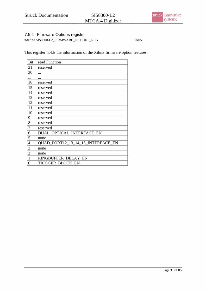
7.5.4 Firmware Options register#define SIS8300-L2_FIRMWARE_OPTIONS_REG 0x05
This register holds the information of the Xilinx firmware option features.
Bit read Function31 reserved30 ...... ...16 reserved15 reserved14 reserved13 reserved12 reserved11 reserved10 reserved9 reserved8 reserved7 reserved6 DUAL_OPTICAL_INTERFACE_EN5 none4 QUAD_PORT12_13_14_15_INTERFACE_EN3 none2 none1 RINGBUFFER_DELAY_EN0 TRIGGER_BLOCK_EN
Struck Documentation SIS8300-L2MTCA.4 Digitizer
Page 32 of 85
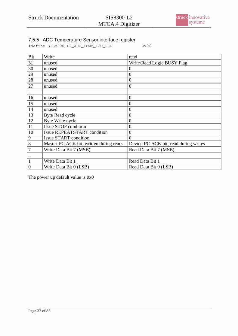
7.5.5 ADC Temperature Sensor interface register#define SIS8300-L2_ADC_TEMP_I2C_REG 0x06
Bit Write read31 unused Write/Read Logic BUSY Flag30 unused 029 unused 028 unused 027 unused 0..16 unused 015 unused 014 unused 013 Byte Read cycle 012 Byte Write cycle 011 Issue STOP condition 010 Issue REPEATSTART condition 09 Issue START condition 08 Master I²C ACK bit, written during reads Device I²C ACK bit, read during writes7 Write Data Bit 7 (MSB) Read Data Bit 7 (MSB)..1 Write Data Bit 1 Read Data Bit 10 Write Data Bit 0 (LSB) Read Data Bit 0 (LSB)
The power up default value is 0x0
Struck Documentation SIS8300-L2MTCA.4 Digitizer
Page 33 of 85
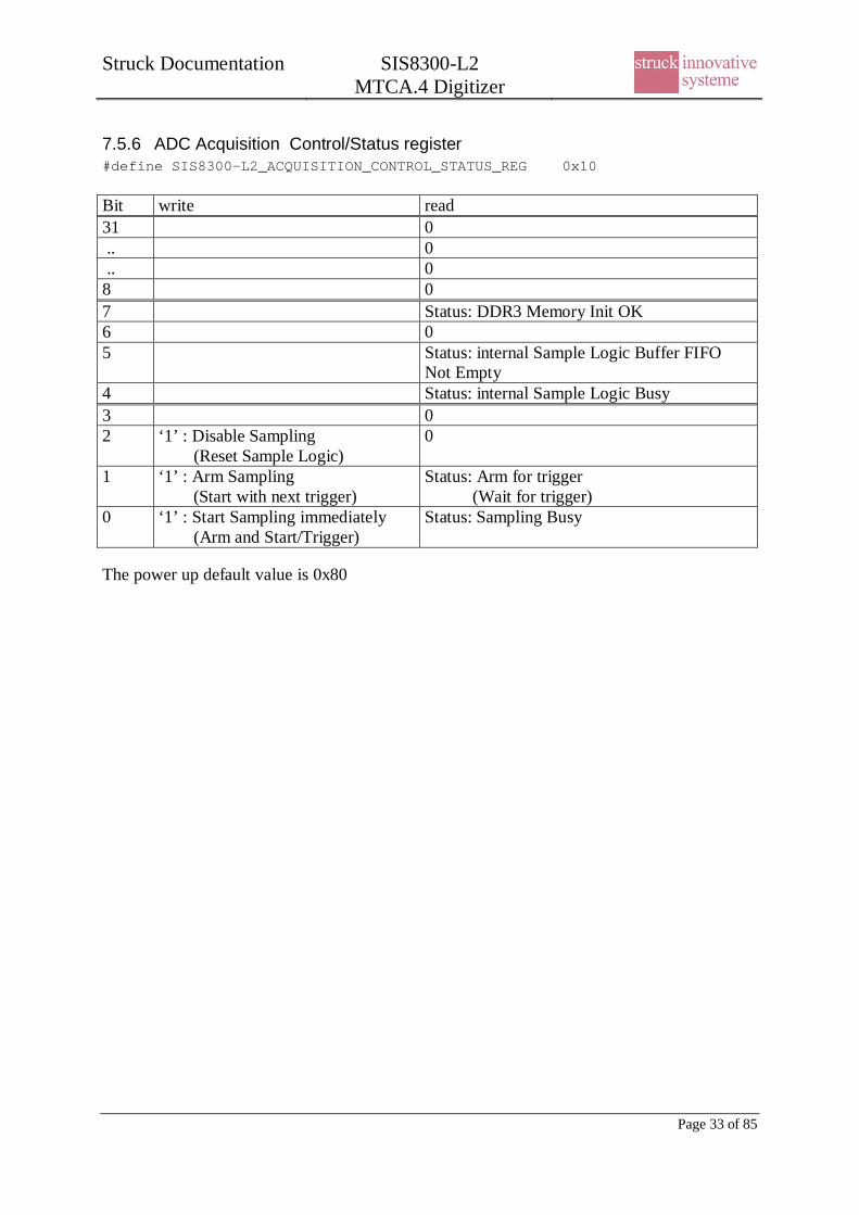
7.5.6 ADC Acquisition Control/Status register#define SIS8300-L2_ACQUISITION_CONTROL_STATUS_REG 0x10
Bit write read31 0 .. 0 .. 08 07 Status: DDR3 Memory Init OK6 05 Status: internal Sample Logic Buffer FIFO
Not Empty4 Status: internal Sample Logic Busy3 02 ‘1’ : Disable Sampling
(Reset Sample Logic)0
1 ‘1’ : Arm Sampling (Start with next trigger)
Status: Arm for trigger (Wait for trigger)
0 ‘1’ : Start Sampling immediately (Arm and Start/Trigger)
Status: Sampling Busy
The power up default value is 0x80
Struck Documentation SIS8300-L2MTCA.4 Digitizer
Page 34 of 85
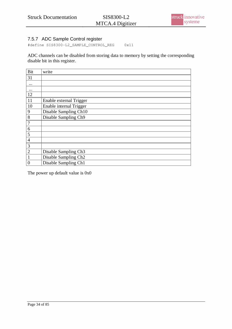
7.5.7 ADC Sample Control register#define SIS8300-L2_SAMPLE_CONTROL_REG 0x11
ADC channels can be disabled from storing data to memory by setting the correspondingdisable bit in this register.
Bit write31 ... ...1211 Enable external Trigger10 Enable internal Trigger9 Disable Sampling Ch108 Disable Sampling Ch9765432 Disable Sampling Ch31 Disable Sampling Ch20 Disable Sampling Ch1
The power up default value is 0x0
Struck Documentation SIS8300-L2MTCA.4 Digitizer
Page 35 of 85
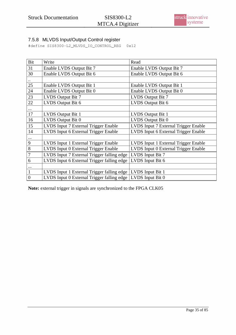
7.5.8 MLVDS Input/Output Control register#define SIS8300-L2_MLVDS_IO_CONTROL_REG 0x12
Bit Write Read31 Enable LVDS Output Bit 7 Enable LVDS Output Bit 730 Enable LVDS Output Bit 6 Enable LVDS Output Bit 6..25 Enable LVDS Output Bit 1 Enable LVDS Output Bit 124 Enable LVDS Output Bit 0 Enable LVDS Output Bit 023 LVDS Output Bit 7 LVDS Output Bit 722 LVDS Output Bit 6 LVDS Output Bit 6...17 LVDS Output Bit 1 LVDS Output Bit 116 LVDS Output Bit 0 LVDS Output Bit 015 LVDS Input 7 External Trigger Enable LVDS Input 7 External Trigger Enable14 LVDS Input 6 External Trigger Enable LVDS Input 6 External Trigger Enable...9 LVDS Input 1 External Trigger Enable LVDS Input 1 External Trigger Enable8 LVDS Input 0 External Trigger Enable LVDS Input 0 External Trigger Enable7 LVDS Input 7 External Trigger falling edge LVDS Input Bit 76 LVDS Input 6 External Trigger falling edge LVDS Input Bit 6...1 LVDS Input 1 External Trigger falling edge LVDS Input Bit 10 LVDS Input 0 External Trigger falling edge LVDS Input Bit 0
Note: external trigger in signals are synchronized to the FPGA CLK05
Struck Documentation SIS8300-L2MTCA.4 Digitizer
Page 36 of 85
7.5.9 Harlink Connector Input/Output Control register#define SIS8300-L2_HARLINK_IO_CONTROL_REG 0x13
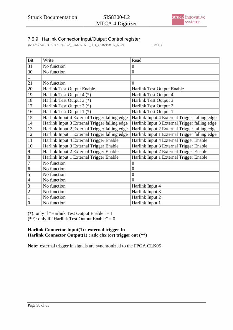
Bit Write Read31 No function 030 No function 0..21 No function 020 Harlink Test Output Enable Harlink Test Output Enable19 Harlink Test Output 4 (*) Harlink Test Output 418 Harlink Test Output 3 (*) Harlink Test Output 317 Harlink Test Output 2 (*) Harlink Test Output 216 Harlink Test Output 1 (*) Harlink Test Output 115 Harlink Input 4 External Trigger falling edge Harlink Input 4 External Trigger falling edge14 Harlink Input 3 External Trigger falling edge Harlink Input 3 External Trigger falling edge13 Harlink Input 2 External Trigger falling edge Harlink Input 2 External Trigger falling edge12 Harlink Input 1 External Trigger falling edge Harlink Input 1 External Trigger falling edge11 Harlink Input 4 External Trigger Enable Harlink Input 4 External Trigger Enable10 Harlink Input 3 External Trigger Enable Harlink Input 3 External Trigger Enable9 Harlink Input 2 External Trigger Enable Harlink Input 2 External Trigger Enable8 Harlink Input 1 External Trigger Enable Harlink Input 1 External Trigger Enable7 No function 06 No function 05 No function 04 No function 03 No function Harlink Input 42 No function Harlink Input 31 No function Harlink Input 20 No function Harlink Input 1
(*): only if “Harlink Test Output Enable” = 1(**): only if “Harlink Test Output Enable” = 0
Harlink Connector Input(1) : external trigger InHarlink Connector Output(1) : adc chx (or) trigger out (**)
Note: external trigger in signals are synchronized to the FPGA CLK05
Struck Documentation SIS8300-L2MTCA.4 Digitizer
Page 37 of 85
7.5.10 Link1 Data FIFO#define SIS8300-L2_LINK1_FIFO_DATA_REG 0x14
Bit Write Read31 Transmit Data D31 Received Data D31
D30 D30… … …
D1 D10 Transmit Data D0 Received Data D0
The power up default value is 0x0
Struck Documentation SIS8300-L2MTCA.4 Digitizer
Page 38 of 85
7.5.11 Link1 Control Register#define SIS8300-L2_LINK1_FIFO_CONTROL_REG 0x15
Bit Write Read31 FIFO reset 030 Receive-FIFO enable 029 0 028 .. 027 Port 14 linkup26 … Port 12 linkup25 0 Opt 1 linkup24 Set to send a protocol word Indicates an protocol word into receive-FIFO23 0 022 … 021 020 Out_fifo_write count D819 D718 …17161514 …13 D112 Out_fifo_write count D011 010 09 08 In_fifo_read count D87 D76 ...54 …3 GTX reset (depending on ‘Link select’)2 Opt1 and Opt2 reset …1 Link select D1(0: Opt1 2: Port12 3: Port14) D10 Link select D0 In_fifo_read count D0
Note: The connection between the links must be initialized:Set Bit 24 = 1 and write 0x1C000000 to 0x14

Struck Documentation SIS8300-L2MTCA.4 Digitizer
Page 39 of 85
7.5.12 Link2 Data FIFO#define SIS8300-L2_LINK2_FIFO_DATA_REG 0x16
Bit Write Read31 Transmit Data D31 Received Data D31
D30 D30… …
D1 D10 Transmit Data D0 Received Data D0
The power up default value is 0x0

Struck Documentation SIS8300-L2MTCA.4 Digitizer
Page 40 of 85
7.5.13 Link2 Control Register#define SIS8300-L2_LINK2_FIFO_CONTROL_REG 0x17
Bit Write Read31 FIFO reset 030 Receive-FIFO enable 029 0 028 .. 027 Port 15 linkup26 … Port 13 linkup25 0 Opt 2 linkup24 Set to send a protocol word Indicates an protocol word into receive-fifo23 0 022 … 021 020 Out_fifo_write count D819 D718 …17161514 …13 D112 Out_fifo_write count D011 010 09 08 In_fifo_read count D87 D76 ...54 …3 GTX reset (depending on ‘Link select’)2 Opt1 and Opt 2 reset …1 Link select D1(0: Opt2 2: Port13 3: Port 15) D10 Link select D0 In_fifo_read count D0
Note: The connection between the links must be initialized:Set Bit 24 = 1 and write 0x1C000000 to 0x16
Struck Documentation SIS8300-L2MTCA.4 Digitizer
Page 41 of 85
7.5.14 Clock Distribution Multiplexer control register#define SIS8300-L2_CLOCK_DISTRIBUTION_MUX_REG 0x40
The SIS8300-L2 has 5 IDT ICS853S057 clock multiplexer chips, which are labelled A to E inthe clock distribution scheme in section 2.8. The multiplexer control register holds the twoselect bits for the 5 multiplexer chips as shown in the table below.The assignment of the inputs to the resources (i.e. clock inputs) is listed in subsection7.5.14.1.
BIT access Name Function
31-12FFFFF000
R/W reserved no
11-1000000C00
R/W MUXE_SEL Multiplexer E select bits
9-800000300
R/W MUXD_SEL Multiplexer D select bits
7-6000000C0
R/W reserved no
5-400000030
R/W MUXC_SEL Multiplexer C select bits
3-20000000C
R/W MUXB_SEL Multiplexer B select bits
1-000000003
R/W MUXA_SEL Multiplexer A select bits
Struck Documentation SIS8300-L2MTCA.4 Digitizer
Page 42 of 85
7.5.14.1 Multiplexer A Input Signals:U222 - Sel0 and Sel1 (MUX1A_SEL) = Multiplexer A select lines
Sel1 Sel0 Selected Input - Net Name Clock source Description0 0 RTMCLK_0 Clock 2 from µRTM card0 1 TCLKB_0 Clock 2 (Telecom Clock B) from AMC Connector (Backplane)1 0 TCLKA_0 Clock 1 (Telecom Clock A) from AMC Connector (Backplane)1 1 OSC_CLK0 Onboard Clock chip (250MHz)
7.5.14.2 Multiplexer B Input Signals:U223 - Sel0 and Sel1 (MUX1B_SEL) = Multiplexer B select lines
Sel1 Sel0 Selected Input - Net Name Clock source Description0 0 RTMCLK_1 Clock 2 from µRTM card0 1 TCLKB_1 Clock 2 (Telecom Clock B) from AMC Connector (Backplane)1 0 TCLKA_1 Clock 1 (Telecom Clock A) from AMC Connector (Backplane)1 1 OSC_CLK1 Onboard Clock chip (250MHz)
7.5.14.3 Multiplexer C Input Signals:U240 - Sel0 and Sel1 (MUXAB_SEL) = Multiplexer C select lines
Sel1 Sel0 Selected Input - Net Name Clock source Description0 0 EXT_CLKB0 Clock from Harlink Connector “CI1-4 IN” (front panel)0 1 EXT_CLKA0 Clock from SMA Connector “CLK IN” (front panel)1 0 MUXA_CLK1 Multiplexer A Output Signal1 1 MUXB_CLK1 Multiplexer B Output Signal
7.5.14.4 Multiplexer D Input Signals:U250 - Sel0 and Sel1 (MUX2A_SEL) = Multiplexer D select lines
Sel1 Sel0 Selected Input - Net Name Clock source Description0 0 MUXA_CLK0 Multiplexer A Output Signal0 1 MUL_CLK1 Clock Multiplier (U242) Output 2 Signal1 0 EXT_CLKB1 Clock from Harlink Connector “CI1-4 IN” (front panel)1 1 EXT_CLKA1 Clock from SMA Connector “CLK IN” (front panel)
7.5.14.5 Multiplexer E Input Signals:U251 - Sel0 and Sel1 (MUX2B_SEL) = Multiplexer E select lines
Sel1 Sel0 Selected Input - Net Name Clock source Description0 0 MUXB_CLK0 Multiplexer B Output Signal0 1 MUL_CLK0 Clock Multiplier (U242) Output 1 Signal1 0 EXT_CLKB2 Clock from Harlink Connector “CI1-4 IN” (front panel)1 1 EXT_CLKA2 Clock from SMA Connector “CLK IN” (front panel)
Struck Documentation SIS8300-L2MTCA.4 Digitizer
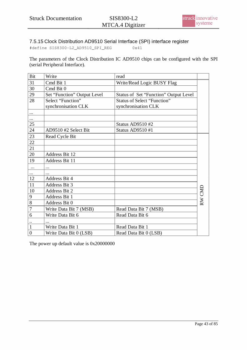
Page 43 of 85
7.5.15 Clock Distribution AD9510 Serial Interface (SPI) interface register#define SIS8300-L2_AD9510_SPI_REG 0x41
The parameters of the Clock Distribution IC AD9510 chips can be configured with the SPI(serial Peripheral Interface).
Bit Write read31 Cmd Bit 1 Write/Read Logic BUSY Flag30 Cmd Bit 029 Set “Function” Output Level Status of Set “Function” Output Level28 Select “Function”
synchronisation CLKStatus of Select “Function”synchronisation CLK
...
...25 Status AD9510 #224 AD9510 #2 Select Bit Status AD9510 #123 Read Cycle Bit222120 Address Bit 1219 Address Bit 11 ... ...... ...12 Address Bit 411 Address Bit 310 Address Bit 29 Address Bit 18 Address Bit 07 Write Data Bit 7 (MSB) Read Data Bit 7 (MSB)6 Write Data Bit 6 Read Data Bit 6.. ...1 Write Data Bit 1 Read Data Bit 10 Write Data Bit 0 (LSB) Read Data Bit 0 (LSB)
RW
CM
D
The power up default value is 0x20000000
Struck Documentation SIS8300-L2MTCA.4 Digitizer
Page 44 of 85
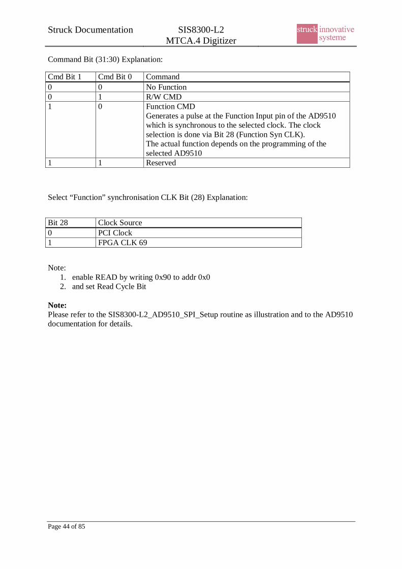
Command Bit (31:30) Explanation:
Cmd Bit 1 Cmd Bit 0 Command0 0 No Function0 1 R/W CMD1 0 Function CMD
Generates a pulse at the Function Input pin of the AD9510which is synchronous to the selected clock. The clockselection is done via Bit 28 (Function Syn CLK).The actual function depends on the programming of theselected AD9510
1 1 Reserved
Select “Function” synchronisation CLK Bit (28) Explanation:
Bit 28 Clock Source0 PCI Clock1 FPGA CLK 69
Note:1. enable READ by writing 0x90 to addr 0x02. and set Read Cycle Bit
Note:Please refer to the SIS8300-L2_AD9510_SPI_Setup routine as illustration and to the AD9510documentation for details.
Struck Documentation SIS8300-L2MTCA.4 Digitizer
Page 45 of 85
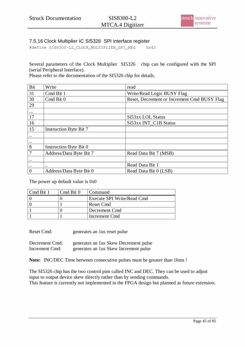
7.5.16 Clock Multiplier IC SI5326 SPI interface register#define SIS8300-L2_CLOCK_MULTIPLIER_SPI_REG 0x42
Several parameters of the Clock Multiplier SI5326 chip can be configured with the SPI(serial Peripheral Interface).Please refer to the documentation of the SI5326 chip for details.
Bit Write read31 Cmd Bit 1 Write/Read Logic BUSY Flag30 Cmd Bit 0 Reset, Decrement or Increment Cmd BUSY Flag29...17 Si53xx LOL Status16 Si53xx INT_C1B Status15 Instruction Byte Bit 7....8 Instruction Byte Bit 07 Address/Data Byte Bit 7 Read Data Bit 7 (MSB).... .. Read Data Bit 10 Address/Data Byte Bit 0 Read Data Bit 0 (LSB)
The power up default value is 0x0
Cmd Bit 1 Cmd Bit 0 Command0 0 Execute SPI Write/Read Cmd0 1 Reset Cmd1 0 Decrement Cmd1 1 Increment Cmd
Reset Cmd: generates an 1us reset pulse
Decrement Cmd: generates an 1us Skew Decrement pulseIncrement Cmd: generates an 1us Skew Increment pulse
Note: INC/DEC Time between consecutive pulses must be greater than 16ms !
The SI5326 chip has the two control pins called INC and DEC. They can be used to adjustinput to output device skew directly rather than by sending commands.This feature is currently not implemented in the FPGA design but planned as future extension.
Struck Documentation SIS8300-L2MTCA.4 Digitizer
Page 46 of 85
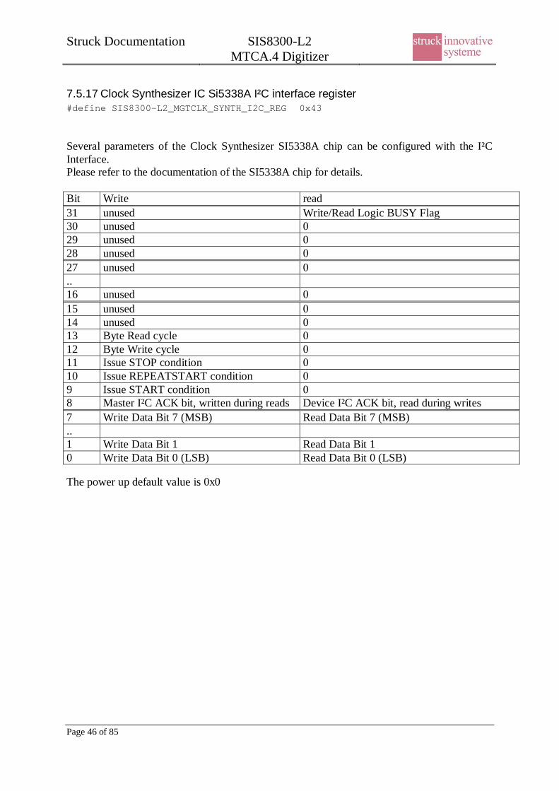
7.5.17 Clock Synthesizer IC Si5338A I²C interface register#define SIS8300-L2_MGTCLK_SYNTH_I2C_REG 0x43
Several parameters of the Clock Synthesizer SI5338A chip can be configured with the I²CInterface.Please refer to the documentation of the SI5338A chip for details.
Bit Write read31 unused Write/Read Logic BUSY Flag30 unused 029 unused 028 unused 027 unused 0..16 unused 015 unused 014 unused 013 Byte Read cycle 012 Byte Write cycle 011 Issue STOP condition 010 Issue REPEATSTART condition 09 Issue START condition 08 Master I²C ACK bit, written during reads Device I²C ACK bit, read during writes7 Write Data Bit 7 (MSB) Read Data Bit 7 (MSB)..1 Write Data Bit 1 Read Data Bit 10 Write Data Bit 0 (LSB) Read Data Bit 0 (LSB)
The power up default value is 0x0
Struck Documentation SIS8300-L2MTCA.4 Digitizer
Page 47 of 85
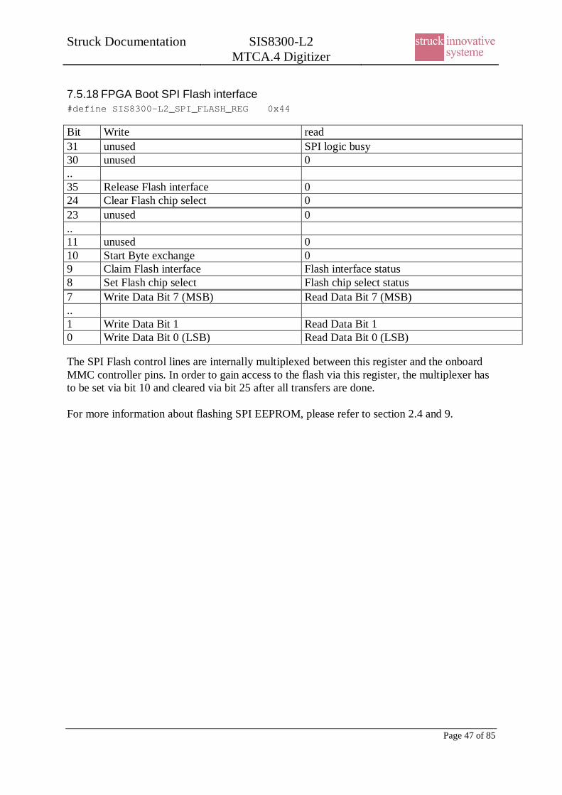
7.5.18 FPGA Boot SPI Flash interface#define SIS8300-L2_SPI_FLASH_REG 0x44
Bit Write read31 unused SPI logic busy30 unused 0..35 Release Flash interface 024 Clear Flash chip select 023 unused 0..11 unused 010 Start Byte exchange 09 Claim Flash interface Flash interface status8 Set Flash chip select Flash chip select status7 Write Data Bit 7 (MSB) Read Data Bit 7 (MSB)..1 Write Data Bit 1 Read Data Bit 10 Write Data Bit 0 (LSB) Read Data Bit 0 (LSB)
The SPI Flash control lines are internally multiplexed between this register and the onboardMMC controller pins. In order to gain access to the flash via this register, the multiplexer hasto be set via bit 10 and cleared via bit 25 after all transfers are done.
For more information about flashing SPI EEPROM, please refer to section 2.4 and 9.
Struck Documentation SIS8300-L2MTCA.4 Digitizer
Page 48 of 85
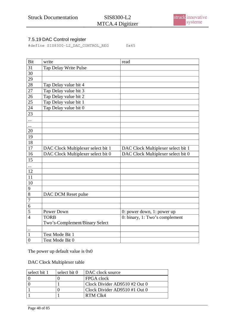
7.5.19 DAC Control register#define SIS8300-L2_DAC_CONTROL_REG 0x45
Bit write read31 Tap Delay Write Pulse302928 Tap Delay value bit 427 Tap Delay value bit 326 Tap Delay value bit 225 Tap Delay value bit 124 Tap Delay value bit 023......20191817 DAC Clock Multiplexer select bit 1 DAC Clock Multiplexer select bit 116 DAC Clock Multiplexer select bit 0 DAC Clock Multiplexer select bit 015...12111098 DAC DCM Reset pulse765 Power Down 0: power down, 1: power up4 TORB
Two’s-Complement/Binary Select0: binary, 1: Two’s complement
..1 Test Mode Bit 10 Test Mode Bit 0
The power up default value is 0x0
DAC Clock Multiplexer table
select bit 1 select bit 0 DAC clock source0 0 FPGA clock0 1 Clock Divider AD9510 #2 Out 01 0 Clock Divider AD9510 #1 Out 01 1 RTM Clk4
Struck Documentation SIS8300-L2MTCA.4 Digitizer
Page 49 of 85
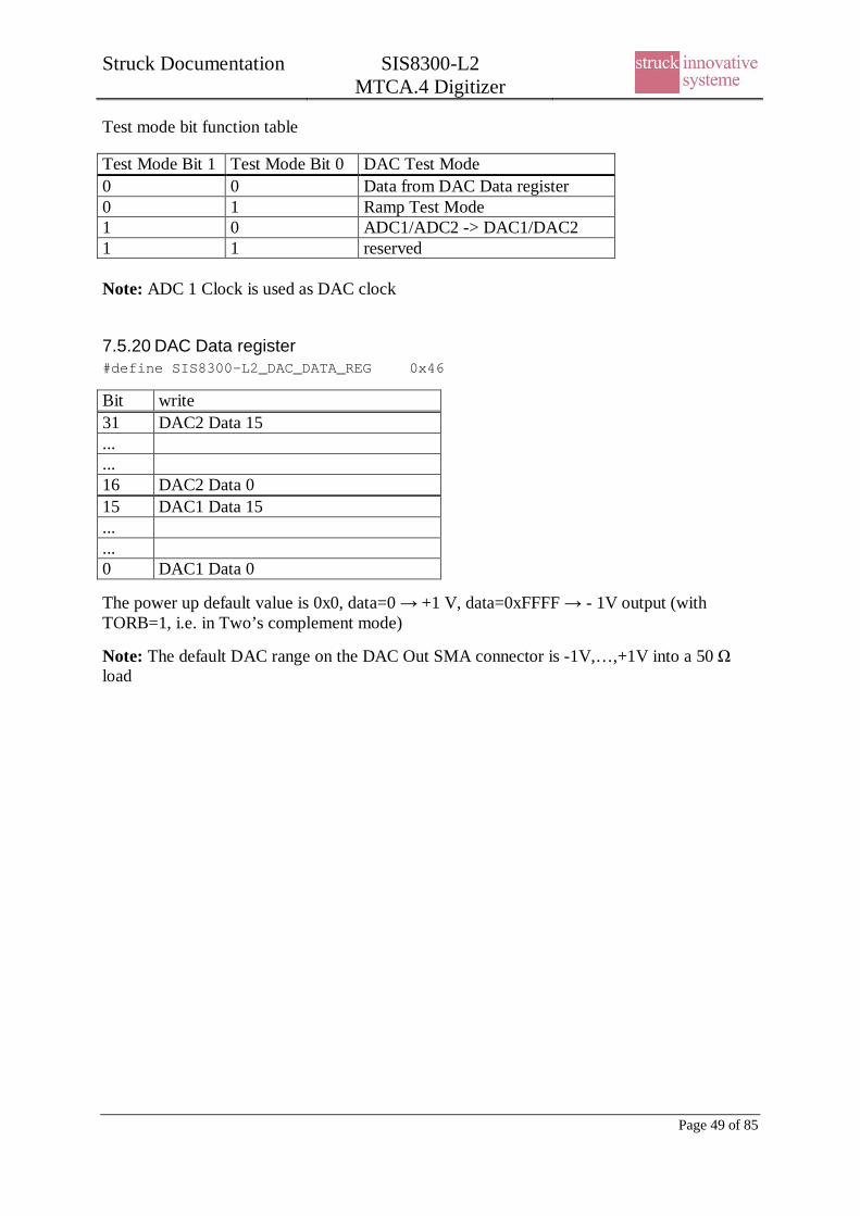
Test mode bit function table
Test Mode Bit 1 Test Mode Bit 0 DAC Test Mode0 0 Data from DAC Data register0 1 Ramp Test Mode1 0 ADC1/ADC2 -> DAC1/DAC21 1 reserved
Note: ADC 1 Clock is used as DAC clock
7.5.20 DAC Data register#define SIS8300-L2_DAC_DATA_REG 0x46
Bit write31 DAC2 Data 15......16 DAC2 Data 015 DAC1 Data 15......0 DAC1 Data 0
The power up default value is 0x0, data=0 +1 V, data=0xFFFF - 1V output (withTORB=1, i.e. in Two’s complement mode)
Note: The default DAC range on the DAC Out SMA connector is -1V,…,+1V into a 50 load
Struck Documentation SIS8300-L2MTCA.4 Digitizer
Page 50 of 85
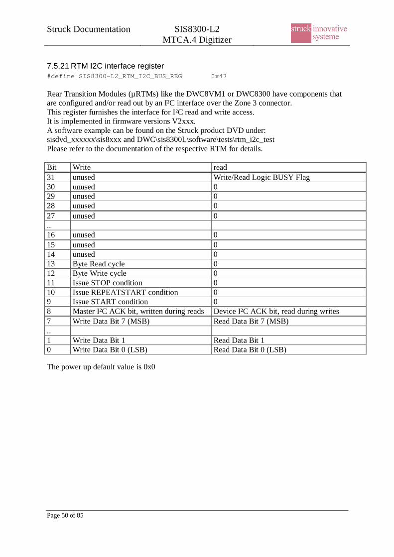
7.5.21 RTM I2C interface register#define SIS8300-L2_RTM_I2C_BUS_REG 0x47
Rear Transition Modules (µRTMs) like the DWC8VM1 or DWC8300 have components thatare configured and/or read out by an I²C interface over the Zone 3 connector.This register furnishes the interface for I²C read and write access.It is implemented in firmware versions V2xxx.A software example can be found on the Struck product DVD under:sisdvd_xxxxxx\sis8xxx and DWC\sis8300L\software\tests\rtm_i2c_testPlease refer to the documentation of the respective RTM for details.
Bit Write read31 unused Write/Read Logic BUSY Flag30 unused 029 unused 028 unused 027 unused 0..16 unused 015 unused 014 unused 013 Byte Read cycle 012 Byte Write cycle 011 Issue STOP condition 010 Issue REPEATSTART condition 09 Issue START condition 08 Master I²C ACK bit, written during reads Device I²C ACK bit, read during writes7 Write Data Bit 7 (MSB) Read Data Bit 7 (MSB)..1 Write Data Bit 1 Read Data Bit 10 Write Data Bit 0 (LSB) Read Data Bit 0 (LSB)
The power up default value is 0x0
Struck Documentation SIS8300-L2MTCA.4 Digitizer
Page 51 of 85
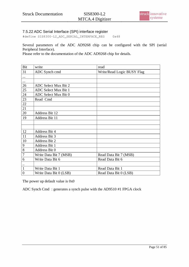
7.5.22 ADC Serial Interface (SPI) interface register#define SIS8300-L2_ADC_SERIAL_INTERFACE_REG 0x48
Several parameters of the ADC AD9268 chip can be configured with the SPI (serialPeripheral Interface).Please refer to the documentation of the ADC AD9268 chip for details.
Bit write read31 ADC Synch cmd Write/Read Logic BUSY Flag......26 ADC Select Mux Bit 225 ADC Select Mux Bit 124 ADC Select Mux Bit 023 Read Cmd222120 Address Bit 1219 Address Bit 11
12 Address Bit 411 Address Bit 310 Address Bit 29 Address Bit 18 Address Bit 07 Write Data Bit 7 (MSB) Read Data Bit 7 (MSB)6 Write Data Bit 6 Read Data Bit 6..1 Write Data Bit 1 Read Data Bit 10 Write Data Bit 0 (LSB) Read Data Bit 0 (LSB)
The power up default value is 0x0
ADC Synch Cmd : generates a synch pulse with the AD9510 #1 FPGA clock
Struck Documentation SIS8300-L2MTCA.4 Digitizer
Page 52 of 85
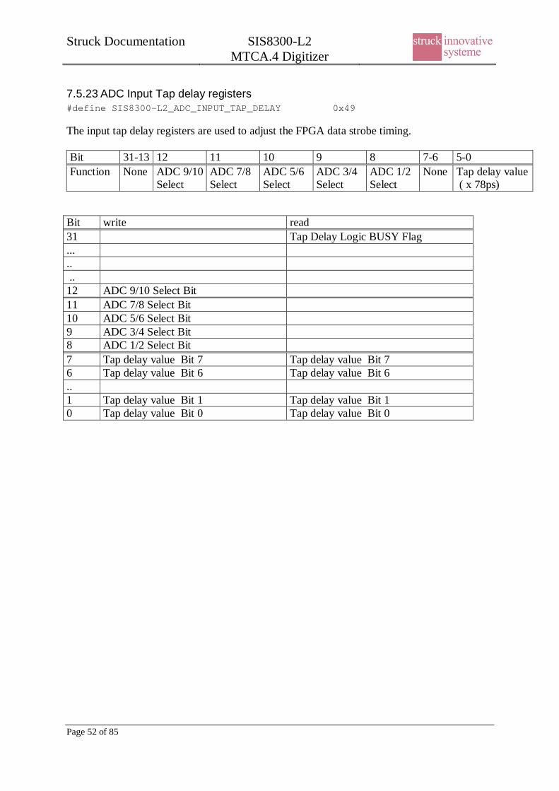
7.5.23 ADC Input Tap delay registers#define SIS8300-L2_ADC_INPUT_TAP_DELAY 0x49
The input tap delay registers are used to adjust the FPGA data strobe timing.
Bit 31-13 12 11 10 9 8 7-6 5-0Function None ADC 9/10
SelectADC 7/8Select
ADC 5/6Select
ADC 3/4Select
ADC 1/2Select
None Tap delay value ( x 78ps)
Bit write read31 Tap Delay Logic BUSY Flag..... ..12 ADC 9/10 Select Bit11 ADC 7/8 Select Bit10 ADC 5/6 Select Bit9 ADC 3/4 Select Bit8 ADC 1/2 Select Bit7 Tap delay value Bit 7 Tap delay value Bit 76 Tap delay value Bit 6 Tap delay value Bit 6..1 Tap delay value Bit 1 Tap delay value Bit 10 Tap delay value Bit 0 Tap delay value Bit 0
Struck Documentation SIS8300-L2MTCA.4 Digitizer
Page 53 of 85
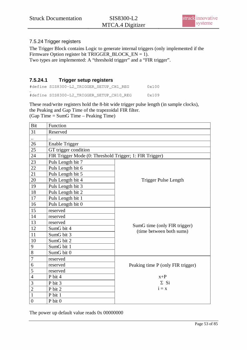
7.5.24 Trigger registersThe Trigger Block contains Logic to generate internal triggers (only implemented if theFirmware Option register bit TRIGGER_BLOCK_EN = 1).Two types are implemented: A “threshold trigger” and a “FIR trigger”.
7.5.24.1 Trigger setup registers#define SIS8300-L2_TRIGGER_SETUP_CH1_REG 0x100..#define SIS8300-L2_TRIGGER_SETUP_CH10_REG 0x109
These read/write registers hold the 8-bit wide trigger pulse length (in sample clocks),the Peaking and Gap Time of the trapezoidal FIR filter.(Gap Time = SumG Time – Peaking Time)
Bit Function31 Reserved.. ..26 Enable Trigger25 GT trigger condition24 FIR Trigger Mode (0: Threshold Trigger; 1: FIR Trigger)23 Puls Length bit 722 Puls Length bit 621 Puls Length bit 520 Puls Length bit 419 Puls Length bit 318 Puls Length bit 217 Puls Length bit 116 Puls Length bit 0
Trigger Pulse Length
15 reserved14 reserved13 reserved12 SumG bit 411 SumG bit 310 SumG bit 29 SumG bit 18 SumG bit 0
SumG time (only FIR trigger)(time between both sums)
7 reserved6 reserved5 reserved4 P bit 43 P bit 32 P bit 21 P bit 10 P bit 0
Peaking time P (only FIR trigger)
x+P Si
i = x
The power up default value reads 0x 00000000
Struck Documentation SIS8300-L2MTCA.4 Digitizer
Page 54 of 85
Si: Sum of ADC input sample stream from x to x+PP: Peaking time (number of values to sum)SumG: SumGap time (distance in clock ticks of the two running sums)
The maximum SumG time: 16 (clocks)The minimun SumG time: 1 (clocks)Values > 16 will be set to 16Value = 0 will be set to 1
The maximum Peaking time: 16 (clocks)The minimun Peaking time: 1 (clocks)Values > 16 will be set to 16Value = 0 will be set to 1
7.5.24.2 Trigger Threshold registers
#define SIS8300-L2_TRIGGER_THRESHOLD_CH1_REG 0x110..#define SIS8300-L2_TRIGGER_THRESHOLD_CH10_REG 0x119
These read/write registers hold the threshold values for the 10 ADC channels.
7.5.24.2.1 Trigger ThresholdFIR Trigger Mode = 0
Bit 31-16 15-0Function Threshold value OFF Threshold value ON
default after Reset: 0x0
A trigger output pulse is generated on two conditions:
GT is set (GT) in trigger setup register:the trigger Out pulse will be issued if the actual sampled ADC value goes above thethreshold value ON and OFF. A new Trigger Out Pulse will be suppressed until theADC value goes below the threshold value OFF.
GT is cleared (LT) in trigger setup register:the trigger Out pulse will be issued if the actual sampled ADC value goes below thethreshold value ON and OFF. A new trigger Out pulse will be suppressed until the ADCvalue goes above the threshold value OFF.
the trigger Out pulse will be issued if the actual sampled ADC value goes below thethreshold value.
GT: greater thanLT: lower than
Struck Documentation SIS8300-L2MTCA.4 Digitizer
Page 55 of 85
7.5.24.2.2 FIR Trigger ThresholdFIR Trigger Mode = 1
Bit 31-20 19-0Function None Trapezoidal threshold value
default after Reset: 0x0
The value of the Sum (trapezoidal value) depends on the peaking time P. Therefore theselection of the value of the Trapezoidal threshold depends on P also.
Trapezoidal value calculation:Trapezoidal value = (SUM2 – SUM1)
Wherex+P
SUM1 = Si i = x
x+P+sumG
SUM2 = Sj j = x+sumG
The FIR filter logic generates the Trapezoidal by subtraction of the two running sums.This implies, that the internal value of the trapezoid is on average 0.
A trigger output pulse is generated:
GT is set (GT):the Trigger Out Pulse will be issued if the actual trapezoidal value goes above theprogrammable trapezoidal threshold value
GT is cleared (LT):the Trigger Out Pulse will be issued if the actual trapezoidal value goes below thenegated programmable trapezoidal threshold value
Struck Documentation SIS8300-L2MTCA.4 Digitizer
Page 56 of 85
7.5.25 Memory Sample Start Block Address / Actual Sample Block Address registers
#define SIS8300-L2_SAMPLE_START_ADDRESS_CH1_REG 0x120..#define SIS8300-L2_SAMPLE_START_ADDRESS_CH10_REG 0x129
The write function to these registers defines the memory start block address.The value is given in 256-bit blocks.
Write Function: ADC chx Memory Sample Start Block AddressBit 31-26 25-0
reserved Memory Sample Start Block Address (256-bit blocks)(16-bit word address x 16)
default after Reset: 0x0
Explanation (memory sample start block address)The contents of the sample memory start block address register is assigned as memory datastorage address with the arm command (key address arm sampling) or with the enablecommand (key address enable sampling).
The read function from these registers give the information of the actual sampling blockaddress for the given ADC channel.(at the moment: only valid if the logic is not busy!)
Read Function : ADC chx Actual Sample Block AddressBit 31-26 25-0
reserved Actual Sample Block Address (in 256-bit Blocks)(16-bit word address x 16)
The value is given in 256-bit Blocks (16bit word address x 16)
Struck Documentation SIS8300-L2MTCA.4 Digitizer
Page 57 of 85
7.5.26 Sample Block Length register
#define SIS8300-L2_SAMPLE_LENGTH_REG 0x12A
This register defines the number of sample blocks of each ADC channel.
The size of one sample block for each ADC channel is 256-bit (16 x 16-bit word).
Bit 31-26 25-0Function reserved Sample Block Length
default after reset: 0x0
Sample BlockLengthvalue
Number of samples of each channel(waveform length)
0x0 160x1 320x2 480x3 64.. ..
0x 3FF FFFF(*) 0x 4000 0000 (1.073.741.824)
* maximum block length of one channel only !
7.5.27 Ringbuffer Delay register
#define SIS8300-L2_PRETRIGGER_DELAY_REG 0x12B
This register defines the number of pre trigger delay samples for all channels.The maximum pre trigger delay value is 2046.
Bit 31-12 11-0Function reserved Delay value

Struck Documentation SIS8300-L2MTCA.4 Digitizer
Page 58 of 85
7.5.28 SIS8900 RTM LVDS Test Input/Output Control register#define SIS8300-L2_RTM_LVDS_IO_CONTROL_REG 0x12F
Bit Write Read31 - Z3 Class Flag30 - 029 Enable RTM LVDS Output Bit 11 (*) Enable RTM LVDS Output Bit D 11 (*)28 Enable RTM LVDS Output Bit 10 (*) Enable RTM LVDS Output Bit D 10 (*)27 Enable RTM LVDS Output Bit 9 (*,#) Enable RTM LVDS Output Bit D 9 (*,#)26 Enable RTM LVDS Output Bit 8 Enable RTM LVDS Output Bit D 825 Enable RTM LVDS Output Bit 7 Enable RTM LVDS Output Bit D 724 Enable RTM LVDS Output Bit 6 Enable RTM LVDS Output Bit D 623 - 022 - 021 RTM LVDS Output Bit D 11 (*) RTM LVDS Output Bit D 11 (*)20 RTM LVDS Output Bit D 10 (*) RTM LVDS Output Bit D 10 (*)19 RTM LVDS Output Bit D 9 (*,#) RTM LVDS Output Bit D 9 (*,#)18 RTM LVDS Output Bit D 8 RTM LVDS Output Bit D 817 RTM LVDS Output Bit D 7 RTM LVDS Output Bit D 716 RTM LVDS Output Bit D 6 RTM LVDS Output Bit D 615 - 014 - 013 - 012 - RTM Z3 TCLK select11 - RTM Z3 TCLK enable10 RTM Z3 ILOCK enable RTM Z3 ILOCK enable9 RTM Z3 ILOCK1 RTM Z3 ILOCK18 RTM Z3 ILOCK0 RTM Z3 ILOCK07 - 06 - 05 - RTM LVDS Input Bit D54 - RTM LVDS Input Bit D43 - RTM LVDS Input Bit D3 (~)2 - RTM LVDS Input Bit D2 (*)1 - RTM LVDS Input Bit D1 (*)0 - RTM LVDS Input Bit D0 (*)
(*): not available if board is configured for Zone 3 Class A1.1CO compatibility(#): not available if board is configured for Zone 3 Class A1.0C compatibility(~): not available if FW versions 83022xxx, signal lines are used for µRTM-USER-I²Csupport, bit always returned as 0x0
Struck Documentation SIS8300-L2MTCA.4 Digitizer
Page 59 of 85
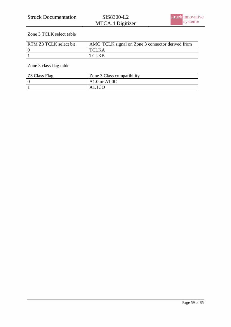
Zone 3 TCLK select table
RTM Z3 TCLK select bit AMC_TCLK signal on Zone 3 connector derived from0 TCLKA1 TCLKB
Zone 3 class flag table
Z3 Class Flag Zone 3 Class compatibility0 A1.0 or A1.0C1 A1.1CO
Struck Documentation SIS8300-L2MTCA.4 Digitizer
Page 60 of 85
7.5.29 Read DMA System Destination address (lower 32bits)
#define DMA_READ_DST_ADR_LO32 0x200
This register holds the lower 32bits of the destination address (byte address !) in systemmemory into which the card will transfer data.
Bit 31-0Function System memory address (lower 32bits)
7.5.30 Read DMA System Destination address (upper 32bits)
#define DMA_READ_DST_ADR_HI32 0x201
This register holds the upper 32bits of the destination address (byte address !) in systemmemory into which the card will transfer data.
Bit 31-0Function System memory address (upper 32bits)
7.5.31 Read DMA Card Memory Source address
#define DMA_READ_SRC_ADR_LO32 0x202
This register holds the 32bit source (byte) address in the card’s address space which is used toselect the data source which is read from.
Bit 31-0Function Card address space
The address layout is:
DDR3 Memory:Address 0x0 - 0x7FFFFFFF: DDR3 selected Memory
User DMA space:Address 0x80000000 - 0xAFFFFFFF: Repeated User DMA space
Note: The Card address must be start on a 64-Byte boundary.0x0, 0x40, 0x80 …
Struck Documentation SIS8300-L2MTCA.4 Digitizer
Page 61 of 85
7.5.32 Read DMA Transfer length
#define DMA_READ_LEN 0x203
This register holds the amount of data (bytes !) which is going to be transferred.
Bit 31-0Function DMA Transfer length
Note: The DMA Transfer length must be a multiple of 64 Bytes.0x40, 0x80, 0xC0 ….
7.5.33 Read DMA Control
#define DMA_READ_CTRL 0x204
This register starts the Read DMA process and allows to poll the transfer status.
Bit write read31 unused 0... 01 unused 00 Start DMA DMA running
Struck Documentation SIS8300-L2MTCA.4 Digitizer
Page 62 of 85
7.5.34 Readout DMA Sample byte swap
#define DMA_READ_BYTESWAP 0x205
This register allows swapping each byte in a sample for optimizing data handling on big/littleendian machines.
Example for disabled swapping:
Byte address offset: Sample value00 Sample 0 lo byte (LSB)01 Sample 0 hi byte (MSB)02 Sample 1 lo byte (LSB)03 Sample 1 hi byte (MSB)
Example for enabled swapping:
Byte address offset: Sample value00 Sample 0 hi byte (MSB)01 Sample 0 lo byte (LSB)02 Sample 1 hi byte (MSB)03 Sample 1 lo byte (LSB)
Bit write read31 unused 0... 01 unused 00 Byteswap enable Byteswap enable status
Struck Documentation SIS8300-L2MTCA.4 Digitizer
Page 63 of 85
7.5.35 Write DMA System Source address (lower 32bits)
#define DMA_WRITE_DST_ADR_LO32 0x210
This register holds the lower 32bits of the destination address (byte address !) in systemmemory from which the card will transfer data.
Bit 31-0Function System memory address (lower 32bits)
7.5.36 Write DMA System Source address (upper 32bits)
#define DMA_WRITE_DST_ADR_HI32 0x211
This register holds the upper 32bits of the destination address (byte address !) in systemmemory from which the card will transfer data.
Bit 31-0Function System memory address (upper 32bits)
7.5.37 Write DMA Card Memory Destination address
#define DMA_WRITE_DST_ADR_LO32 0x212
This register holds the 32bit destination (byte) address in the cards address space which isused to select the data source which is written to.
Bit 31-0Function Card address space
The address layout is:
DDR3 Memory:Address 0x0 - 0x7FFFFFFF: DDR3 selected Memory
Note: The Card address must be start on a 64-Byte boundary.0x0, 0x40, 0x80 …
Struck Documentation SIS8300-L2MTCA.4 Digitizer
Page 64 of 85
7.5.38 Write DMA Transfer length
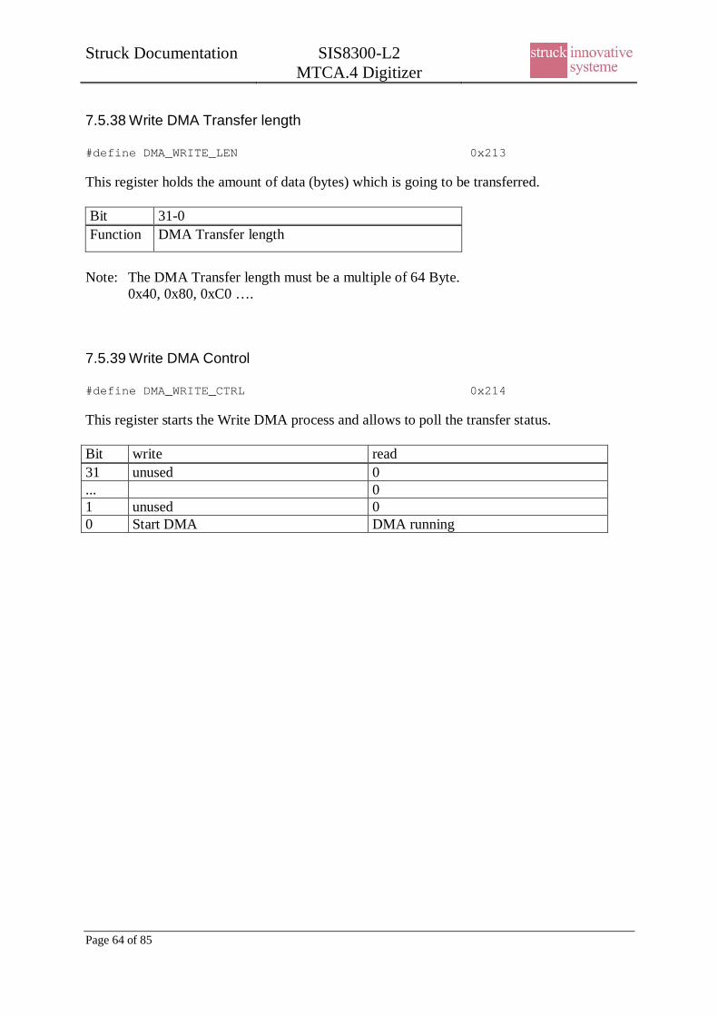
#define DMA_WRITE_LEN 0x213
This register holds the amount of data (bytes) which is going to be transferred.
Bit 31-0Function DMA Transfer length
Note: The DMA Transfer length must be a multiple of 64 Byte.0x40, 0x80, 0xC0 ….
7.5.39 Write DMA Control
#define DMA_WRITE_CTRL 0x214
This register starts the Write DMA process and allows to poll the transfer status.
Bit write read31 unused 0... 01 unused 00 Start DMA DMA running
Struck Documentation SIS8300-L2MTCA.4 Digitizer
Page 65 of 85
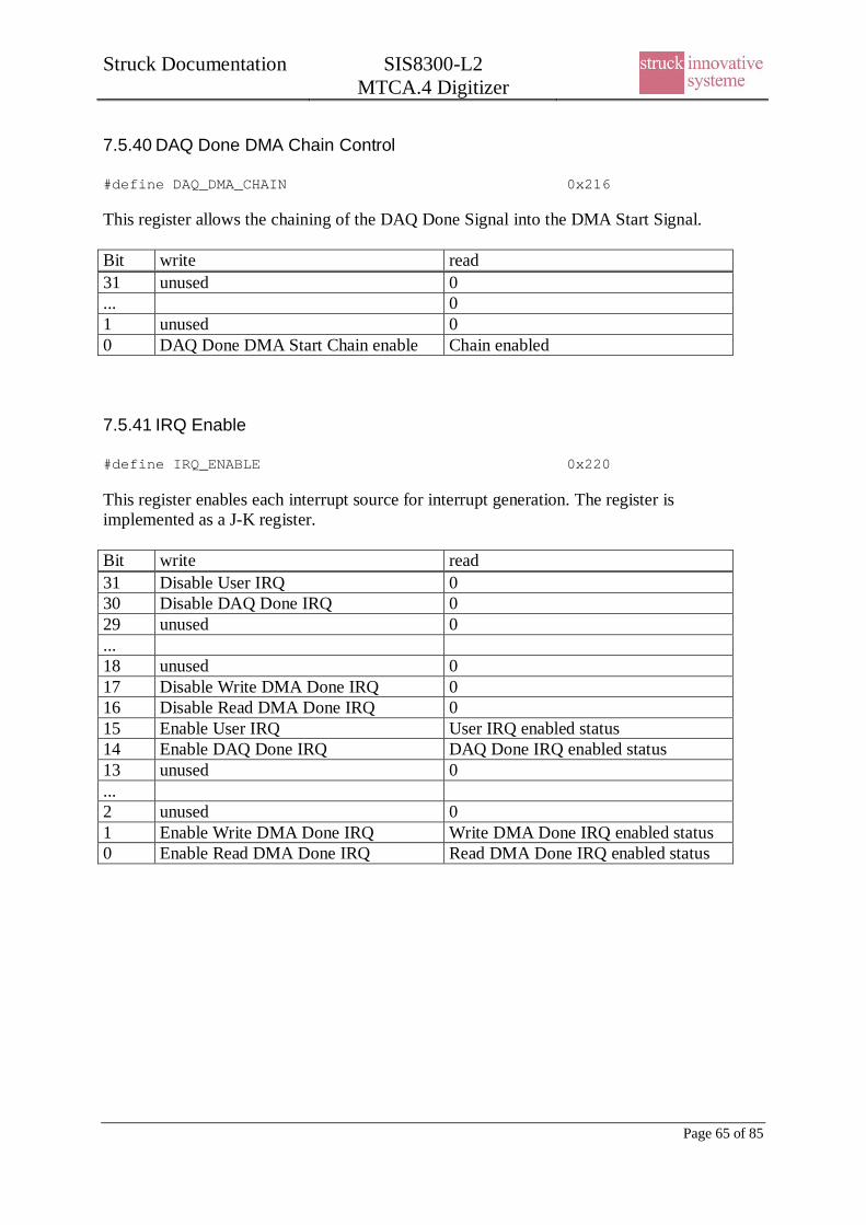
7.5.40 DAQ Done DMA Chain Control
#define DAQ_DMA_CHAIN 0x216
This register allows the chaining of the DAQ Done Signal into the DMA Start Signal.
Bit write read31 unused 0... 01 unused 00 DAQ Done DMA Start Chain enable Chain enabled
7.5.41 IRQ Enable
#define IRQ_ENABLE 0x220
This register enables each interrupt source for interrupt generation. The register isimplemented as a J-K register.
Bit write read31 Disable User IRQ 030 Disable DAQ Done IRQ 029 unused 0...18 unused 017 Disable Write DMA Done IRQ 016 Disable Read DMA Done IRQ 015 Enable User IRQ User IRQ enabled status14 Enable DAQ Done IRQ DAQ Done IRQ enabled status13 unused 0...2 unused 01 Enable Write DMA Done IRQ Write DMA Done IRQ enabled status0 Enable Read DMA Done IRQ Read DMA Done IRQ enabled status
Struck Documentation SIS8300-L2MTCA.4 Digitizer
Page 66 of 85
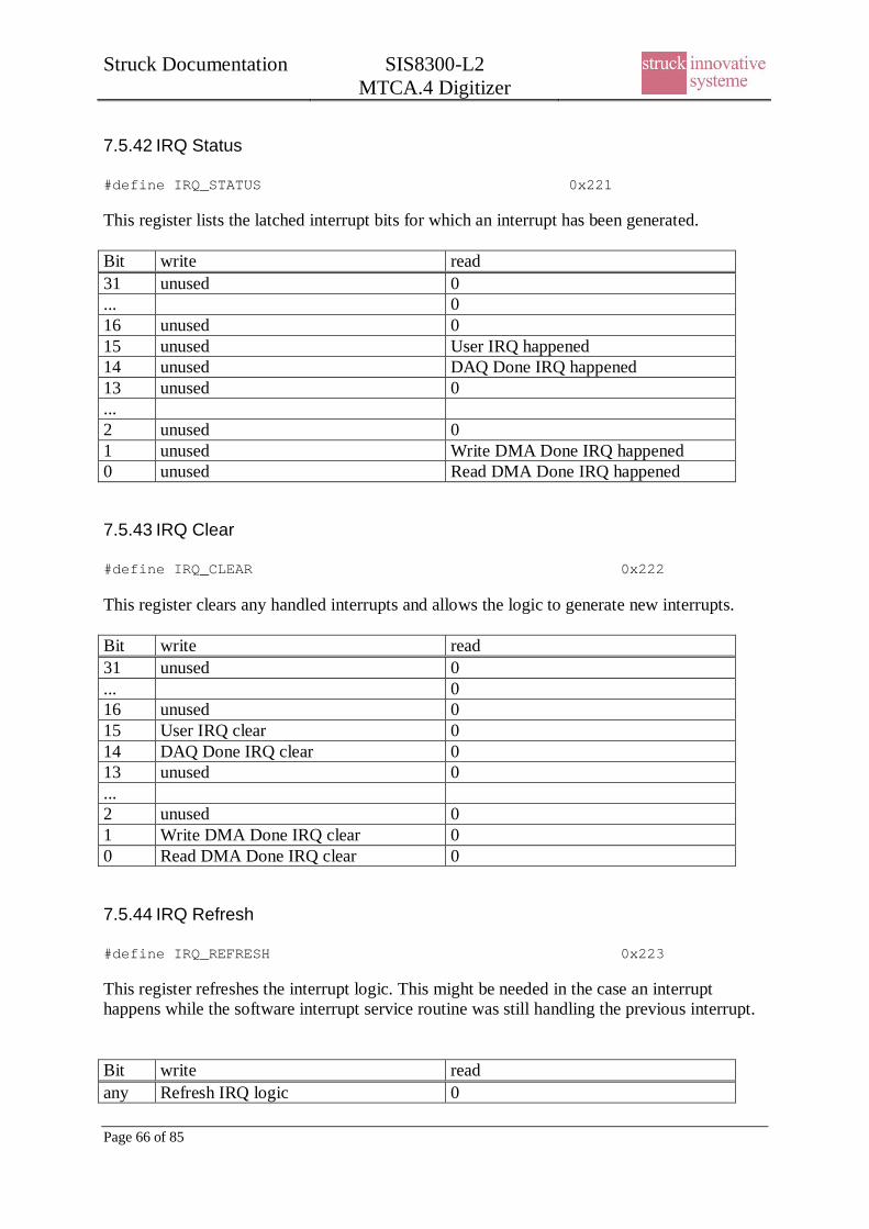
7.5.42 IRQ Status
#define IRQ_STATUS 0x221
This register lists the latched interrupt bits for which an interrupt has been generated.
Bit write read31 unused 0... 016 unused 015 unused User IRQ happened14 unused DAQ Done IRQ happened13 unused 0...2 unused 01 unused Write DMA Done IRQ happened0 unused Read DMA Done IRQ happened
7.5.43 IRQ Clear
#define IRQ_CLEAR 0x222
This register clears any handled interrupts and allows the logic to generate new interrupts.
Bit write read31 unused 0... 016 unused 015 User IRQ clear 014 DAQ Done IRQ clear 013 unused 0...2 unused 01 Write DMA Done IRQ clear 00 Read DMA Done IRQ clear 0
7.5.44 IRQ Refresh
#define IRQ_REFRESH 0x223
This register refreshes the interrupt logic. This might be needed in the case an interrupthappens while the software interrupt service routine was still handling the previous interrupt.
Bit write readany Refresh IRQ logic 0
Struck Documentation SIS8300-L2MTCA.4 Digitizer
Page 67 of 85
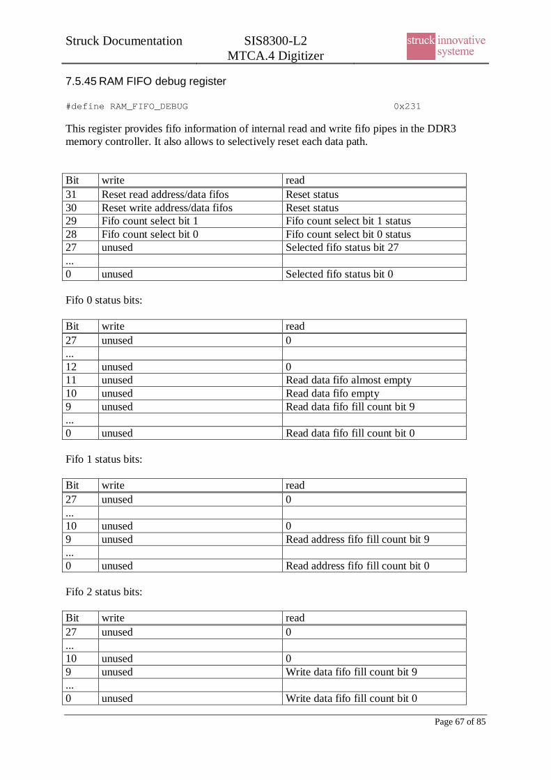
7.5.45 RAM FIFO debug register
#define RAM_FIFO_DEBUG 0x231
This register provides fifo information of internal read and write fifo pipes in the DDR3memory controller. It also allows to selectively reset each data path.
Fifo 0 status bits:
Fifo 1 status bits:
Fifo 2 status bits:
Bit write read31 Reset read address/data fifos Reset status30 Reset write address/data fifos Reset status29 Fifo count select bit 1 Fifo count select bit 1 status28 Fifo count select bit 0 Fifo count select bit 0 status27 unused Selected fifo status bit 27...0 unused Selected fifo status bit 0
Bit write read27 unused 0...12 unused 011 unused Read data fifo almost empty10 unused Read data fifo empty9 unused Read data fifo fill count bit 9...0 unused Read data fifo fill count bit 0
Bit write read27 unused 0...10 unused 09 unused Read address fifo fill count bit 9...0 unused Read address fifo fill count bit 0
Bit write read27 unused 0...10 unused 09 unused Write data fifo fill count bit 9...0 unused Write data fifo fill count bit 0
Struck Documentation SIS8300-L2MTCA.4 Digitizer
Page 68 of 85
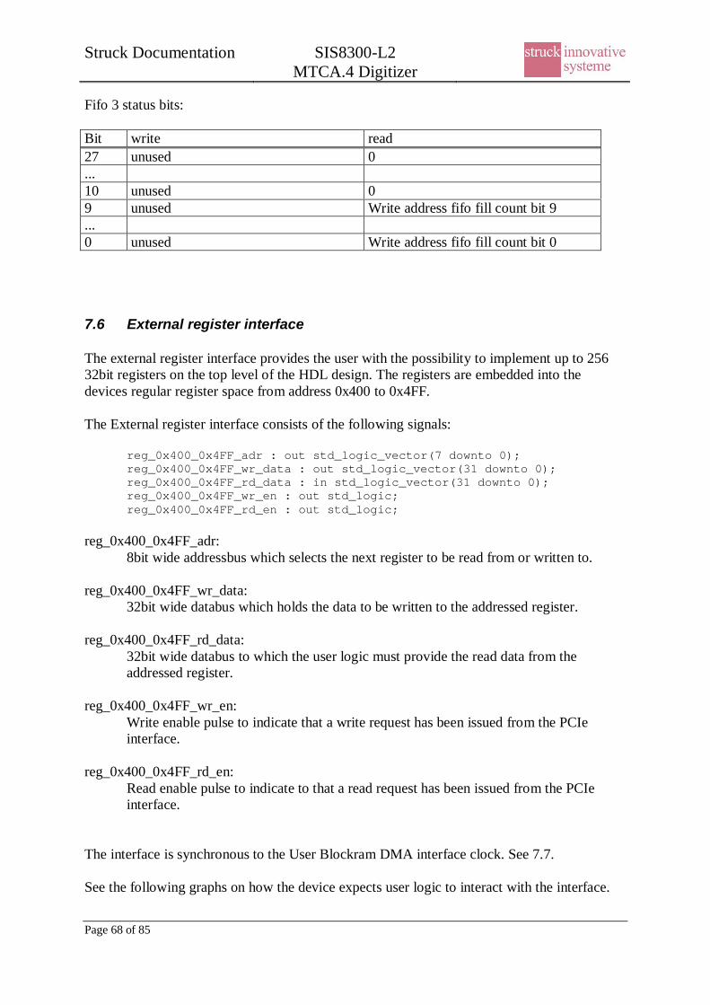
Fifo 3 status bits:
7.6 External register interface
The external register interface provides the user with the possibility to implement up to 25632bit registers on the top level of the HDL design. The registers are embedded into thedevices regular register space from address 0x400 to 0x4FF.
The External register interface consists of the following signals:
reg_0x400_0x4FF_adr : out std_logic_vector(7 downto 0);reg_0x400_0x4FF_wr_data : out std_logic_vector(31 downto 0);reg_0x400_0x4FF_rd_data : in std_logic_vector(31 downto 0);reg_0x400_0x4FF_wr_en : out std_logic;reg_0x400_0x4FF_rd_en : out std_logic;
reg_0x400_0x4FF_adr:8bit wide addressbus which selects the next register to be read from or written to.
reg_0x400_0x4FF_wr_data:32bit wide databus which holds the data to be written to the addressed register.
reg_0x400_0x4FF_rd_data:32bit wide databus to which the user logic must provide the read data from theaddressed register.
reg_0x400_0x4FF_wr_en:Write enable pulse to indicate that a write request has been issued from the PCIeinterface.
reg_0x400_0x4FF_rd_en:Read enable pulse to indicate to that a read request has been issued from the PCIeinterface.
The interface is synchronous to the User Blockram DMA interface clock. See 7.7.
See the following graphs on how the device expects user logic to interact with the interface.
Bit write read27 unused 0...10 unused 09 unused Write address fifo fill count bit 9...0 unused Write address fifo fill count bit 0
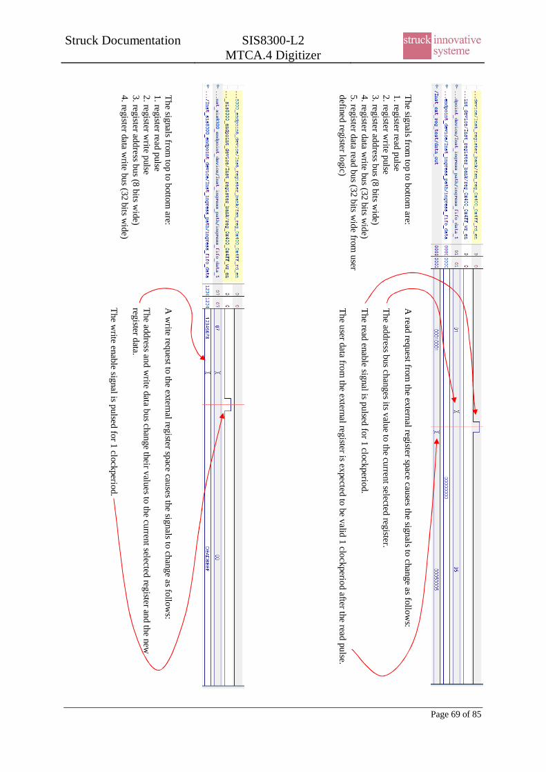
Struck Documentation SIS8300-L2MTCA.4 Digitizer
Page 69 of 85
The signals from top to bottom
are:1. register read pulse2. register w
rite pulse3. register address bus (8 bits w
ide)4. register data w
rite bus (32 bits wide)
The signals from top to bottom
are:1. register read pulse2. register w
rite pulse3. register address bus (8 bits w
ide)4. register data w
rite bus (32 bits wide)
5. register data read bus (32 bits wide from
userdefined register logic)
A w
rite request to the external register space causes the signals to change as follows:
The address and write data bus change their values to the current selected register and the new
register data.
The write enable signal is pulsed for 1 clockperiod.
A read request from
the external register space causes the signals to change as follows:
The address bus changes its value to the current selected register.
The read enable signal is pulsed for 1 clockperiod.
The user data from the external register is expected to be valid 1 clockperiod after the read pulse.
Struck Documentation SIS8300-L2MTCA.4 Digitizer
Page 70 of 85
7.7 User Blockram DMA Interface
The User Blockram DMA interface consists of the following signals:
bram_dma_clk : out std_logic;bram_dma_adr : out std_logic_vector(31 downto 0);bram_dma_rd_en : out std_logic;bram_dma_rd_data : in std_logic_vector(63 downto 0);
bram_dma_clk:Free running 125MHz clock to which the data and control signals are synchronous to
bram_dma_adr:32bit wide addressbus which is mapped over the 512MB of onboard sample RAM.The addresses ranges from 0x00000000 to 0x1FFFFFFF (512MB)
bram_dma_rd_en:(Optional) Read enable pulse for connected logic. The read enable pulse is valid 1clockperiod before the data is expected to be valid on the databus.
bram_dma_rd_data:64bit wide (due to PCIe endpoint design) databus which holds the data to betransmitted over PCIe. The data needs to be valid 1 clockperiod after ram_dma_rd_enis valid.
Note:This interface was built to be directly able to connect to a Xilinx CoreGen generatedblockram module with a 64bit wide read bus. Due to PCIe endpoint design constraints theuser has to read the blockram via DMA in 8byte steps.
7.8 User Interrupt Interface
The User Interrupt interface consists of the following signals.
user_irq : in std_logic;user_irq_clear : out std_logic;
user_irq:User interrupt pulse input to the PCIe endpoint. The connected logic has to supply apulse of at least 1 clockperiod in length to trigger the interrupt logic. If the driver/usersoftware has enabled the corresponding interrupt line, an interrupt is generated on thePCIe interface.
user_irq_clear:A 1 clock period wide pulse which is triggered, when the driver software has servicedthe issued interrupt in the interrupt service routine. This pulse may be used to reset anylogic that depends on user feedback through the software interface.
The interface is synchronous to the User Blockram DMA interface clock. See section 7.7.
Struck Documentation SIS8300-L2MTCA.4 Digitizer
Page 71 of 85
8 µRTM management
Connected µRTMs shall be compliant to the PICMG MTCA.4 specification in a way thatthey must have an on board I²C EEPROM (on address 0x50) and a NXP PCF8574-com-patible port expander (on address 0x7C).
Required port expander connection map for normal operation:
Port pin FunctionP0 Hot Swap Handle (low active)P1 Hot Swap LED (Blue, low active)P2 LED 1 (Red, low active)P3 LED 2 (Green, low active)P4 PowerGood (low active)P5 Reset (low active)P6 PowerEnable (low active)P7 EEPROM Write Protect
The EEPROM shall contain any relevant device information (FRU records) about the µRTM(refer to PICMG AMC.0). Additionally the EEPROM shall contain the new record typesdefined in PICMG MTCA.4.
In order to be able to decide whether a connected µRTM is compatible to the SIS8300-L2 theµRTM record shall contain one of the Zone 3 Identifier listed in the table below.
Supported Zone 3 Identifier (Interface Identifier OEM):
IANA PEN (Privateenterprise number)
Interface IdentifierOEM
Description
0x0092BD (37565) 0x83000002 SIS8300-L2 Zone 3 - compatibility0x00053F (1343) 0x08020000 DESY DWC Zone 3 compatibility0x0092BD (37565) 0x89000001 SIS8900 Zone3 - v1 compatibility
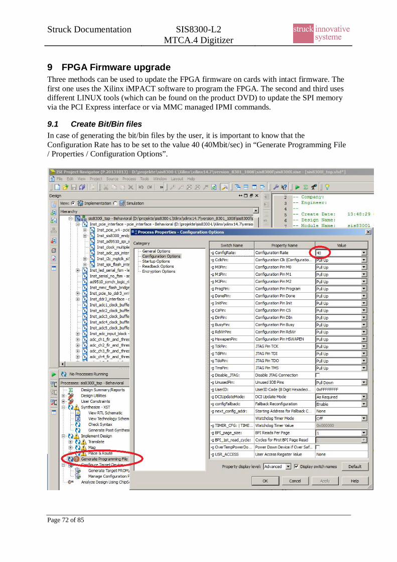
Struck Documentation SIS8300-L2MTCA.4 Digitizer
Page 72 of 85
9 FPGA Firmware upgradeThree methods can be used to update the FPGA firmware on cards with intact firmware. Thefirst one uses the Xilinx iMPACT software to program the FPGA. The second and third usesdifferent LINUX tools (which can be found on the product DVD) to update the SPI memoryvia the PCI Express interface or via MMC managed IPMI commands.
9.1 Create Bit/Bin filesIn case of generating the bit/bin files by the user, it is important to know that theConfiguration Rate has to be set to the value 40 (40Mbit/sec) in “Generate Programming File/ Properties / Configuration Options”.
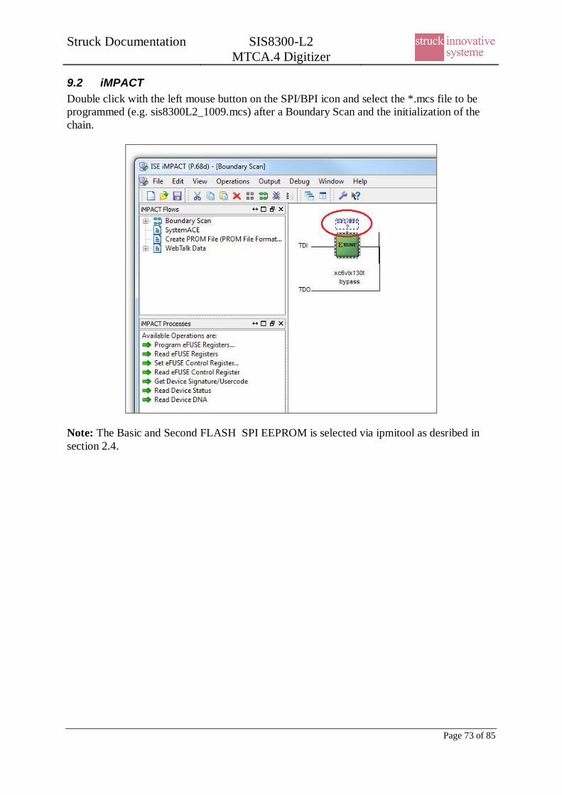
Struck Documentation SIS8300-L2MTCA.4 Digitizer
Page 73 of 85
9.2 iMPACTDouble click with the left mouse button on the SPI/BPI icon and select the *.mcs file to beprogrammed (e.g. sis8300L2_1009.mcs) after a Boundary Scan and the initialization of thechain.
Note: The Basic and Second FLASH SPI EEPROM is selected via ipmitool as desribed insection 2.4.
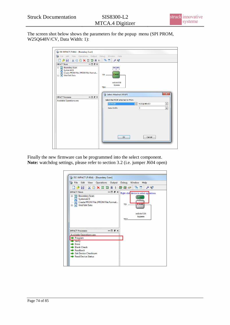
Struck Documentation SIS8300-L2MTCA.4 Digitizer
Page 74 of 85
The screen shot below shows the parameters for the popup menu (SPI PROM,W25Q648V/CV, Data Width: 1):
Finally the new firmware can be programmed into the select component.Note: watchdog settings, please refer to section 3.2 (i.e. jumper J604 open)
Struck Documentation SIS8300-L2MTCA.4 Digitizer
Page 75 of 85
9.3 Linux tool ‘flashupdater’This method can not be used on cards with flawed firmware.To be able to use this tool, it is required that the driver is loaded and the devices are mountedproperly. Use the commands below for verification:
# lsmod | grep sis Result (if driver loaded): sis8300drv
# ls /dev/ | grep sis Result: for each installed device one entry (sis8300-0e.g.)
Now the update can be started:
./flashupdate <path/to/file>.bin
9.4 Linux tool ‘ipmitool’The last from four methods of upgrading is to upload FPGA firmware via IPMI.This can be made with LINUX software ipmitool.
ipmitool ... (not implemented yet, please request us for more information)
9.5 Linux workaround for PCIe-Hot-PlugDuring the firmware development phase it may be of interest to re-establish PCIe connectivityto the SIS8300-L without a power cycle of the crate. A workaround is given in the commandsequence below.
1. Open a terminal and deactivate the Struck device driver:sudo rmmod sis8300drv
2. Change into the root space:sudo su
3. Disable the PCIe link of the target device slot (e.g. slot number 5):
echo 0 > /sys/bus/pci/slots/5/power
The link LED (L1) goes off.
4. 5. Reactivate the PCIe slot:
echo 1 > /sys/bus/pci/slots/5/power
The link LED (L1) goes back on.
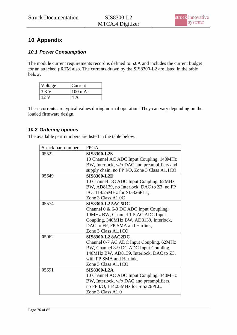
Struck Documentation SIS8300-L2MTCA.4 Digitizer
Page 76 of 85
10 Appendix
10.1 Power Consumption
The module current requirements record is defined to 5.0A and includes the current budgetfor an attached µRTM also. The currents drawn by the SIS8300-L2 are listed in the tablebelow.
Voltage Current3.3 V 100 mA12 V 4 A
These currents are typical values during normal operation. They can vary depending on theloaded firmware design.
10.2 Ordering optionsThe available part numbers are listed in the table below.
Struck part number FPGA05522 SIS8300-L2S
10 Channel AC ADC Input Coupling, 140MHzBW, Interlock, w/o DAC and preamplifiers andsupply chain, no FP I/O, Zone 3 Class A1.1CO
05649 SIS8300-L2D10 Channel DC ADC Input Coupling, 62MHzBW, AD8139, no Interlock, DAC to Z3, no FPI/O, 114.25MHz for SI5326PLL,Zone 3 Class A1.0C
05574 SIS8300-L2 5AC5DCChannel 0 & 6-9 DC ADC Input Coupling,10MHz BW, Channel 1-5 AC ADC InputCoupling, 340MHz BW, AD8139, Interlock,DAC to FP, FP SMA and Harlink,Zone 3 Class A1.1CO
05962 SIS8300-L2 8AC2DCChannel 0-7 AC ADC Input Coupling, 62MHzBW, Channel 8-9 DC ADC Input Coupling,140MHz BW, AD8139, Interlock, DAC to Z3,with FP SMA and Harlink,Zone 3 Class A1.1CO
05691 SIS8300-L2A10 Channel AC ADC Input Coupling, 340MHzBW, Interlock, w/o DAC and preamplifiers,no FP I/O, 114.25MHz for SI5326PLL,Zone 3 Class A1.0
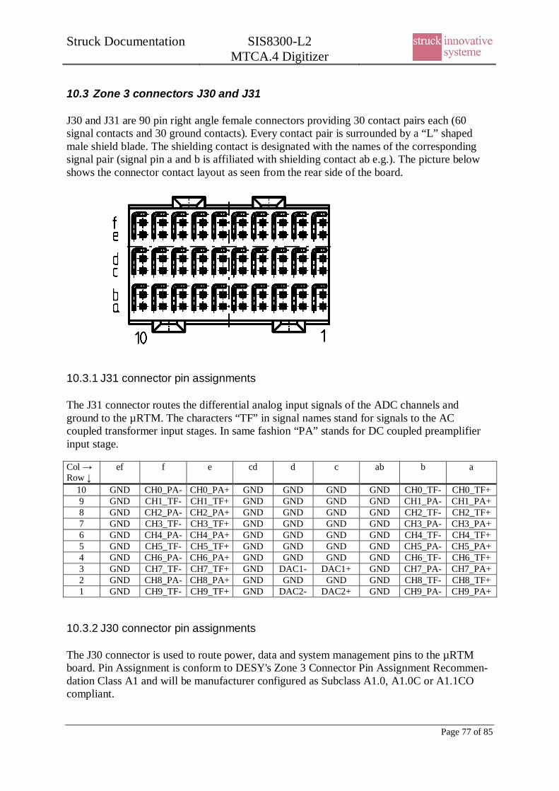
Struck Documentation SIS8300-L2MTCA.4 Digitizer
Page 77 of 85
10.3 Zone 3 connectors J30 and J31
J30 and J31 are 90 pin right angle female connectors providing 30 contact pairs each (60signal contacts and 30 ground contacts). Every contact pair is surrounded by a “L” shapedmale shield blade. The shielding contact is designated with the names of the correspondingsignal pair (signal pin a and b is affiliated with shielding contact ab e.g.). The picture belowshows the connector contact layout as seen from the rear side of the board.
10.3.1 J31 connector pin assignments
The J31 connector routes the differential analog input signals of the ADC channels andground to the µRTM. The characters “TF” in signal names stand for signals to the ACcoupled transformer input stages. In same fashion “PA” stands for DC coupled preamplifierinput stage.
Col Row
ef f e cd d c ab b a
10 GND CH0_PA- CH0_PA+ GND GND GND GND CH0_TF- CH0_TF+9 GND CH1_TF- CH1_TF+ GND GND GND GND CH1_PA- CH1_PA+8 GND CH2_PA- CH2_PA+ GND GND GND GND CH2_TF- CH2_TF+7 GND CH3_TF- CH3_TF+ GND GND GND GND CH3_PA- CH3_PA+6 GND CH4_PA- CH4_PA+ GND GND GND GND CH4_TF- CH4_TF+5 GND CH5_TF- CH5_TF+ GND GND GND GND CH5_PA- CH5_PA+4 GND CH6_PA- CH6_PA+ GND GND GND GND CH6_TF- CH6_TF+3 GND CH7_TF- CH7_TF+ GND DAC1- DAC1+ GND CH7_PA- CH7_PA+2 GND CH8_PA- CH8_PA+ GND GND GND GND CH8_TF- CH8_TF+1 GND CH9_TF- CH9_TF+ GND DAC2- DAC2+ GND CH9_PA- CH9_PA+
10.3.2 J30 connector pin assignments
The J30 connector is used to route power, data and system management pins to the µRTMboard. Pin Assignment is conform to DESY's Zone 3 Connector Pin Assignment Recommen-dation Class A1 and will be manufacturer configured as Subclass A1.0, A1.0C or A1.1COcompliant.
Struck Documentation SIS8300-L2MTCA.4 Digitizer
Page 78 of 85
Pin Assignment for Class A1.0 (assembly option, e.g. SIS8300-L2A)
Col Row
ef f e Cd D c ab b a
10 GND GND GND GND GND GND GND GND GND9 GND CLK1- CLK1+ GND nc nc GND CLK0- CLK0+8 GND CLK5- CLK5+ GND CLK2- CLK2+ GND CLK4- CLK4+7 GND GND GND GND GND GND GND GND GND6 GND D11- D11+ GND D10- D10+ GND D9- D9+5 GND D8- D8+ GND D7- D7+ GND D6- D6+4 GND D5- D5+ GND D4- D4+ GND D3- D3+3 GND D2- D2+ GND D1- D1+ GND D0- D0+2 GND TMS TDI GND SCL MP+3.3V GND PWR+12V PWR+12V1 GND TDO TCK GND SDA PS# GND PWR+12V PWR+12V
Pin Assignment for Class A1.0C (assembly option, e.g. SIS8300-L2D)
Col Row
ef f e Cd D c ab b a
10 GND GND GND GND GND GND GND GND GND9 GND CLK1- CLK1+ GND nc nc GND CLK0- CLK0+8 GND CLK5- CLK5+ GND CLK2- CLK2+ GND CLK4- CLK4+7 GND GND GND GND GND GND GND GND GND6 GND D11- D11+ GND D10- D10+ GND AMC_TCLK- AMC_TCLK-5 GND D8- D8+ GND D7- D7+ GND D6- D6+4 GND D5- D5+ GND D4- D4+ GND D3- D3+3 GND D2- D2+ GND D1- D1+ GND D0- D0+2 GND TMS TDI GND SCL MP+3.3V GND PWR+12V PWR+12V1 GND TDO TCK GND SDA PS# GND PWR+12V PWR+12V
Pin Assignment for Class A1.1CO (default configuration, e.g. SIS8300-L2S)
Col Row
ef f e Cd d c ab b a
10 GND GND GND GND GND GND GND GND GND9 GND CLK1- CLK1+ GND nc nc GND CLK0- CLK0+8 GND CLK5- CLK5+ GND CLK2- CLK2+ GND CLK4- CLK4+7 GND GND GND GND GND GND GND GND GND6 GND OUT1- OUT1+ GND OUT0- OUT0+ GND AMC_TCLK- AMC_TCLK-5 GND D8- D8+ GND D7- D7+ GND D6- D6+4 GND D5- D5+ GND D4- D4+ GND D3- D3+3 GND SFP-TX- SFP-TX+ GND SFP-RX- SFP-RX+ GND SFP-CLK- SFP-CLK+2 GND TMS TDI GND SCL MP+3.3V GND PWR+12V PWR+12V1 GND TDO TCK GND SDA PS# GND PWR+12V PWR+12V
Note: SFP signal pins of row 3 are not connected (open)
For more information about Zone 3 recommendation, please refer tohttp://mtca.desy.de/resources/zone_3_recommendation/index_eng.html
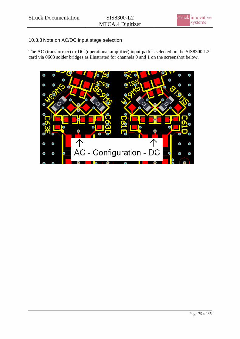
Struck Documentation SIS8300-L2MTCA.4 Digitizer
Page 79 of 85
10.3.3 Note on AC/DC input stage selection
The AC (transformer) or DC (operational amplifier) input path is selected on the SIS8300-L2card via 0603 solder bridges as illustrated for channels 0 and 1 on the screenshot below.
Struck Documentation SIS8300-L2MTCA.4 Digitizer
Page 80 of 85
The designators for all channels can be found in the table below.
ADC Channel Designator Input for ADC0 SW63A ADC_CH0+0 SW63B ADC_CH0-1 SW61A ADC_CH1+1 SW61B ADC_CH1-2 SW58A ADC_CH2+2 SW58B ADC_CH2-3 SW56A ADC_CH3+3 SW56B ADC_CH3-4 SW53A ADC_CH4+4 SW53B ADC_CH4-5 SW51A ADC_CH5+5 SW51B ADC_CH5-6 SW48A ADC_CH6+6 SW48B ADC_CH6-7 SW46A ADC_CH7+7 SW46B ADC_CH7-8 SW43A ADC_CH8+8 SW43B ADC_CH8-9 SW41A ADC_CH9+9 SW41B ADC_CH9-
Note: Keep in mind that filtering components (like antialiasing) may be involved also foryour particular application.
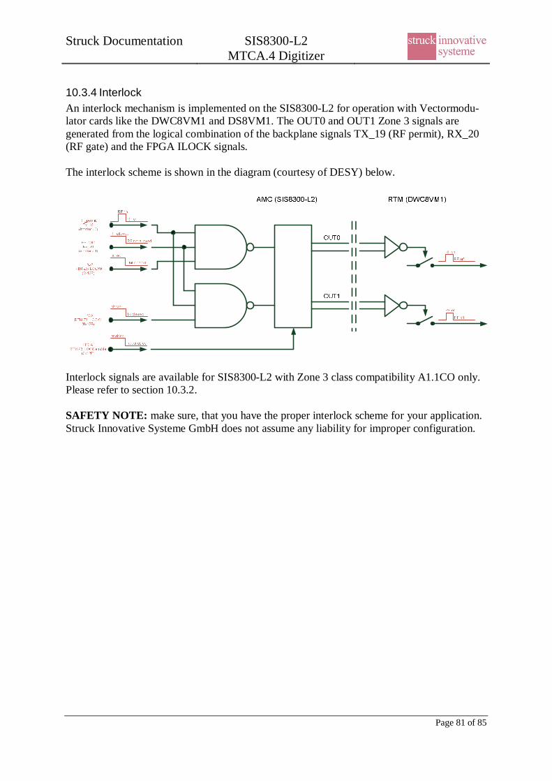
Struck Documentation SIS8300-L2MTCA.4 Digitizer
Page 81 of 85
10.3.4 InterlockAn interlock mechanism is implemented on the SIS8300-L2 for operation with Vectormodu-lator cards like the DWC8VM1 and DS8VM1. The OUT0 and OUT1 Zone 3 signals aregenerated from the logical combination of the backplane signals TX_19 (RF permit), RX_20(RF gate) and the FPGA ILOCK signals.
The interlock scheme is shown in the diagram (courtesy of DESY) below.
Interlock signals are available for SIS8300-L2 with Zone 3 class compatibility A1.1CO only.Please refer to section 10.3.2.
SAFETY NOTE: make sure, that you have the proper interlock scheme for your application.Struck Innovative Systeme GmbH does not assume any liability for improper configuration.
Struck Documentation SIS8300-L2MTCA.4 Digitizer
Page 82 of 85
10.4 Zone 3 connector schematic
Struck Documentation SIS8300-L2MTCA.4 Digitizer
Page 83 of 85
10.5 MMC Readme fileThe license to use the DESY MMC code is granted to Struck Innovative Systeme underlicense contract LV92. Struck and its’ end users are bound to adhere to the contents andconditions of the following Readme file (which can be found on our product DVD also):
DESY MMC end user licence notice v1.0
1
1. The MMC firmware on this device is based on the DESY MMC firmware package.It has been adapted to the device by the device vendor.
2. DESY MMC firmware package is written for operation at DESY and is provided as-is to the device vendor,without any warranty including all implied warranties of merchantability and fitness.In no event shall DESY be liable for any special, direct indirect, or consequential damages,or any damages whatsoever resulting from loss of use, data or profits, whether in an action of contract,negligence or other tortious action, arising out of or in connection with the use or performance of thissoftware.
3. Claims for damages of any nature against DESY are expressly excluded,except in case of gross negligence or wilful misconduct.DESY shall not be liable for any indirect damages or damages caused by assistants.
4. The firmware is distributed as binary code, either on the MMC or as a data package for a firmwareupdate.The end user may not disassemble or reverse-engineer any parts of the MMC firmware.
5. The end user may keep backup copies of the MMC firmware,or copies which are necessary to install the MMC firmware in the end user's MTCA infrastructure.The end user may not distribute the MMC firmware to a third party.
Warning: The MMC firmware has been adapted to a specific device.DO NOT USE MMC FIRMWARE ON A DEVICE IT HAS NOT BEEN ADAPTED TO.USING THE WRONG FIRMWARE CAN CAUSE DAMAGE TO THE DEVICE OR THE MTCA INFRASTRUCTURE IT IS CONNECTED TO.When in doubt contact the device vendor.
Struck Documentation SIS8300-L2MTCA.4 Digitizer
Page 84 of 85
11 Index12 V 76250 MSPS 113,3 V 768-bit 16A 18A1.0 59, 77A1.0C 14, 58, 59, 77A1.1CO 14, 58, 59, 77AC 79AD9268 51AD9510 43, 48ADC Sample Logic 23ADC Temperature Sensor 32Address Map 27AdvancedMC 6AMC 6AMC.0 71AMC_TCLK 14Appendix 76arm 56Atmel 17Atmel-Studio 8ATxmega128 7, 17, 22AVR 8AVR JTAG 17AVR JTAGICE 8Basic FLASH 9binary 48Block diagram 6board layout 22CLK05 12, 35, 36clock
DAC 13input 21RTM 13TCLK 13
clock distribution 12, 15CON600 16connector types 22DAC 22DAC 11
clock 13impedance 11range 11
DACclock multiplexer 48
DACclock multiplexer 49
DACTest mode bits 49
DACrange 49
DACimpedance 49
DAC clock 13, 49DC 79DDR3 24DEC 45design 6DESY 81DESY MMC 7DMA Read 60DS8VM1 81
DVD 11, 50DWC8300 50DWC8VM1 11, 50, 81E-Keying 7ERNI 22external register interface 68FIFO
Link 1 27Link 2 27
firmwareversion 29
Firmware 23Firmware Options
register 31FLASH
Basic 9, 16, 73Second 9, 16, 73
FPGA 6configuration data 9
FPGA CLK05 12, 35, 36FPGA Firmware upgrade 73front panel 20FRU 7, 71functionality 6Harlink 21HARTING 22I2C 29I²C
interface 11I²C interface 11ICS853S057 41IDT 41iMPACT 16, 72INC 45Interlock 81introduction 5IPMI 17ipmitool 8, 9J32 17J33 17J604 16, 74, 78J75 77JBT 22JTAG 10, 16, 22, 27
AVR 17jumper 16JYEBAO 22L1 18, 21L2 18, 21LED 18
20A 19A 18D105A 19D105B 19D110A 19D110B 19D20B 19D20C 19D20D 19D20E 19D20F 19D20G 19D20H 19
Struck Documentation SIS8300-L2MTCA.4 Digitizer
Page 85 of 85
D21D 19L1 18L2 18test 30U 18user 30
LEDsAMC 18Front Panel 18SMD 19
Link 1 27Link 2 27LTC2493 11LVDS 21M 53MAX5878 11mc info 8MCH 7, 17, 18memory interface 24memory write interface 25MGT 15microcontroller 17MMC
firmware upgrade 8Readme file 83sensors 8
MMC V1.00 7MOLEX 22MTCA.4 71multiplexer A 42multiplexer B 42multiplexer C 42multiplexer D 42multiplexer E 42NATView 8NXP 71ordering options 76P 53parallel load 16PCF8574 71PCI Express 6PCIe-HotPlug 75PE2 17PE3 17Platform Management 7Power Consumption 76Read DMA
destination address 60Readme file for MMC 83register
ADC Acquisition Control/Status 33ADC IOB delay 52ADC Sample Control 34ADC serial interface 51clock distribution AD9510 SPI interface 43clock distribution multiplexer control 41Clock Multiplier IC SI5326 SPI interface 45control 29DAC control 48DAC Data 49Firmware Options 31firmware revision 29Harlink Connector Input/Output Control 36
I²C interface 11Memory Sample Start Address 56MLVDS Input/Output Control 35module Id. 29ringbuffer delay 57Sample Length 57serial number 29SIS8900 RTM LVDS Test Input/Output Control
register 58trigger setup 53, 54trigger threshold 54User Control/Status 30
RTM 29, 71clock 13
RTM connector schematics 82RTM connectors 77RTM management 71SAMTEC 22Second FLASH 9sensor
ADC temperature 10sensors 8SFP 6, 21, 22SI5326 45SI5326 12SI5326 45SI5338A 46SIS8900 14SMA 11, 21, 49SPI 9
connectivity 9EEPROM 9FPGA boot FLASH interface 47
TCLKclock 13
TCLKA 59TCLKB 59TE Connectivity 21thermistor 10TORB 48trigger threshold 54Two's complement 48TYCO 22U 18U222 42U223 42U240 42U250 42U251 42U500 16user
LED 30user blockram dma interface 70user interrupt interface 70Vectormodulator 11Virtex 6 6watchdog reset 16Xilinx 6, 72XILINX HW-USB-JTAG 16Z3 58, 59Zone 3 58, 59, 77