Embed Size (px)
Citation preview
Silicon-Tungsten electromagnetic calorimeter
Jean-Claude Brient*
Laboratoire Leprince-RinguetEcole Polytechnique – CNRS
Palaiseau
* co-convener for ECAL-ILD and former spokesperson of CALICE 1
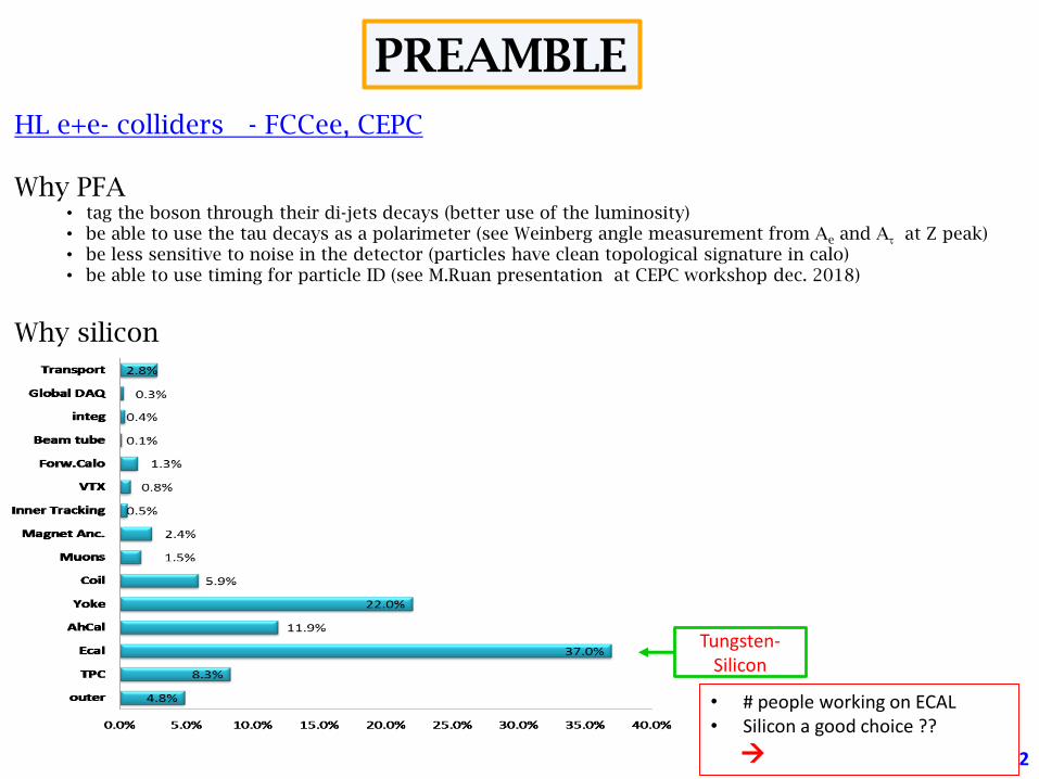
2
HL e+e- colliders - FCCee, CEPC
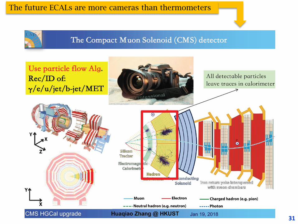
Why PFA• tag the boson through their di-jets decays (better use of the luminosity) • be able to use the tau decays as a polarimeter (see Weinberg angle measurement from Ae and A at Z peak)• be less sensitive to noise in the detector (particles have clean topological signature in calo)• be able to use timing for particle ID (see M.Ruan presentation at CEPC workshop dec. 2018)
Why silicon• PFA needs small pixels size , good S/N at MIP, good linearity, stability• be able to read the energy deposited at high frequency (40 mHz – no slow pulse like in some scintillators)• to run at Z peak with reasonable occupancy (very small pixels size with fast readout)
PREAMBLE
Tungsten-Silicon
• # people working on ECAL• Silicon a good choice ??
3
HL e+e- colliders - FCCee, CEPC
Why PFA• tag the boson through their di-jets decays (better use of the luminosity) • be able to use the tau decays as a polarimeter (see Weinberg angle measurement from A at Z peak)• be less sensitive to noise in the detector (particles have clean topological signature in calo)• be able to use timing for particle ID (see M.Ruan presentation)
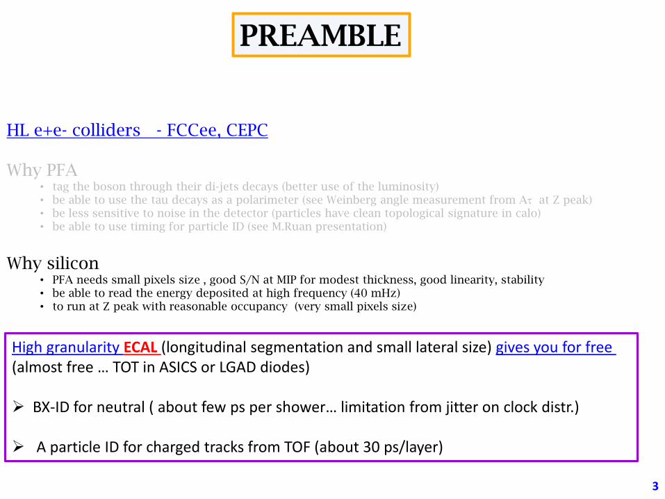
Why silicon• PFA needs small pixels size , good S/N at MIP for modest thickness, good linearity, stability • be able to read the energy deposited at high frequency (40 mHz)• to run at Z peak with reasonable occupancy (very small pixels size)
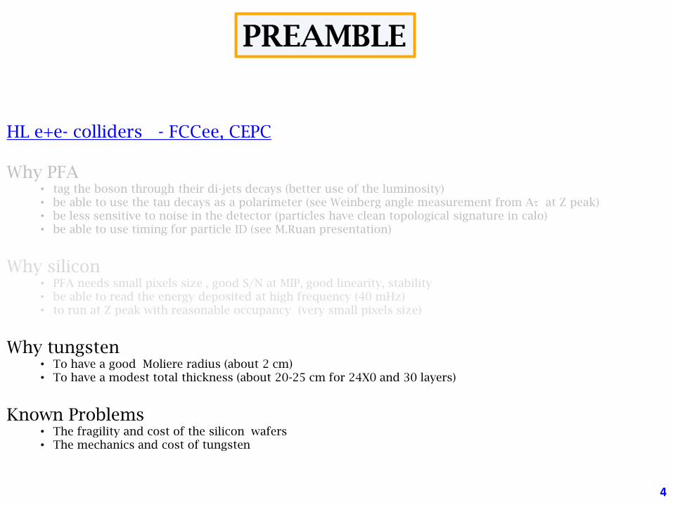
Why tungsten• To have a good Moliere radius (about 2 cm)• To have a modest total thickness (about 20-25 cm for 24X0 and 30 layers)
Known Problems• The fragility and cost of the silicon wafers• The mechanics and cost of tungsten
PREAMBLE
High granularity ECAL (longitudinal segmentation and small lateral size) gives you for free (almost free … TOT in ASICS or LGAD diodes)
BX-ID for neutral ( about few ps per shower… limitation from jitter on clock distr.)
A particle ID for charged tracks from TOF (about 30 ps/layer)
4
HL e+e- colliders - FCCee, CEPC
Why PFA• tag the boson through their di-jets decays (better use of the luminosity) • be able to use the tau decays as a polarimeter (see Weinberg angle measurement from A at Z peak)• be less sensitive to noise in the detector (particles have clean topological signature in calo)• be able to use timing for particle ID (see M.Ruan presentation)
Why silicon• PFA needs small pixels size , good S/N at MIP, good linearity, stability • be able to read the energy deposited at high frequency (40 mHz)• to run at Z peak with reasonable occupancy (very small pixels size)
Why tungsten• To have a good Moliere radius (about 2 cm)• To have a modest total thickness (about 20-25 cm for 24X0 and 30 layers)
Known Problems• The fragility and cost of the silicon wafers• The mechanics and cost of tungsten
PREAMBLE
5
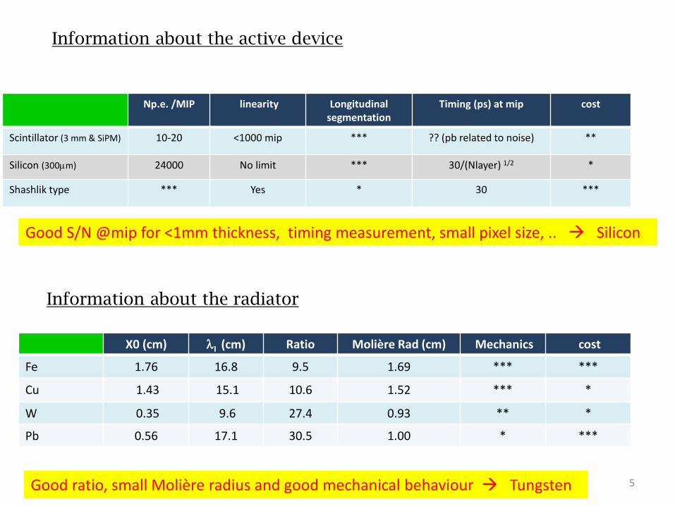
Information about the radiator
Information about the active device
Np.e. /MIP linearity Longitudinal segmentation
Timing (ps) at mip cost
Scintillator (3 mm & SiPM) 10-20 <1000 mip *** ?? (pb related to noise) **
Silicon (300m) 24000 No limit *** 30/(Nlayer) 1/2 *
Shashlik type *** Yes * 30 ***
X0 (cm) I (cm) Ratio Molière Rad (cm) Mechanics cost
Fe 1.76 16.8 9.5 1.69 *** ***
Cu 1.43 15.1 10.6 1.52 *** *
W 0.35 9.6 27.4 0.93 ** *
Pb 0.56 17.1 30.5 1.00 * ***
Good ratio, small Molière radius and good mechanical behaviour Tungsten
Good S/N @mip for <1mm thickness, timing measurement, small pixel size, .. Silicon
6
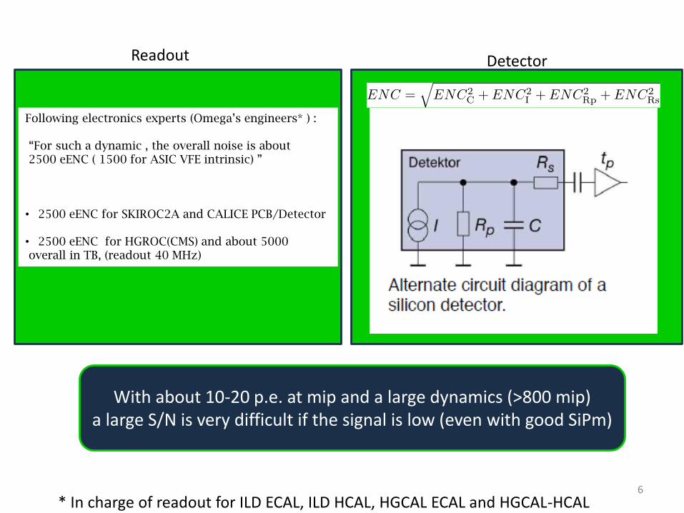
With about 10-20 p.e. at mip and a large dynamics (>800 mip) a large S/N is very difficult if the signal is low (even with good SiPm)
Detector
Following electronics experts (Omega’s engineers* ) :
“For such a dynamic , the overall noise is about2500 eENC ( 1500 for ASIC VFE intrinsic) ”
• 2500 eENC for SKIROC2A and CALICE PCB/Detector
• 2500 eENC for HGROC(CMS) and about 5000overall in TB, (readout 40 MHz)
Readout
* In charge of readout for ILD ECAL, ILD HCAL, HGCAL ECAL and HGCAL-HCAL
7
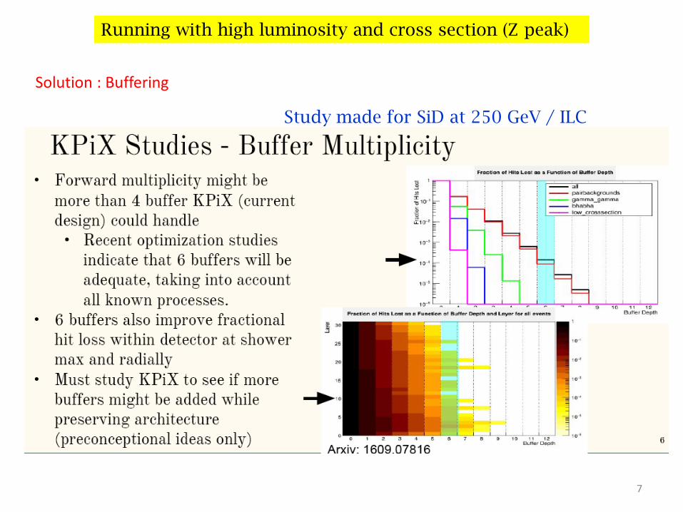
Running with high luminosity and cross section (Z peak)
Solution : Buffering
Study made for SiD at 250 GeV / ILC
8
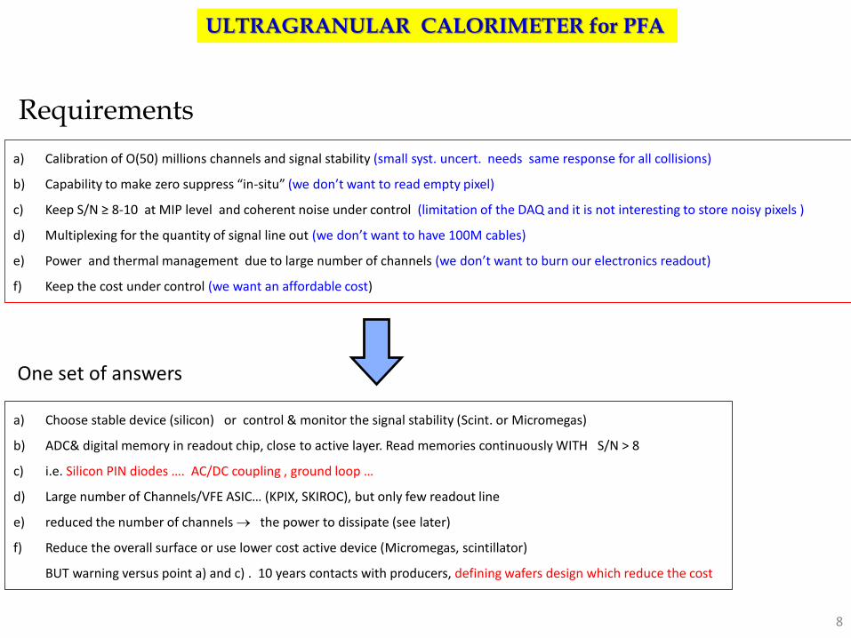
Requirements
a) Calibration of O(50) millions channels and signal stability (small syst. uncert. needs same response for all collisions)
b) Capability to make zero suppress “in-situ” (we don’t want to read empty pixel)
c) Keep S/N ≥ 8-10 at MIP level and coherent noise under control (limitation of the DAQ and it is not interesting to store noisy pixels )
d) Multiplexing for the quantity of signal line out (we don’t want to have 100M cables)
e) Power and thermal management due to large number of channels (we don’t want to burn our electronics readout)
f) Keep the cost under control (we want an affordable cost)
a) Choose stable device (silicon) or control & monitor the signal stability (Scint. or Micromegas)
b) ADC& digital memory in readout chip, close to active layer. Read memories continuously WITH S/N > 8
c) i.e. Silicon PIN diodes …. AC/DC coupling , ground loop …
d) Large number of Channels/VFE ASIC… (KPIX, SKIROC), but only few readout line
e) reduced the number of channels the power to dissipate (see later)
f) Reduce the overall surface or use lower cost active device (Micromegas, scintillator)
BUT warning versus point a) and c) . 10 years contacts with producers, defining wafers design which reduce the cost
One set of answers
ULTRAGRANULAR CALORIMETER for PFA
9
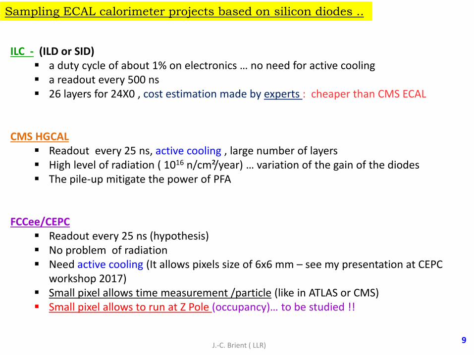
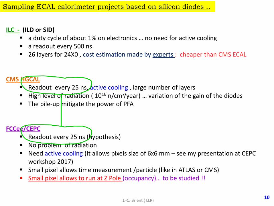
ILC - (ILD or SID) a duty cycle of about 1% on electronics … no need for active cooling a readout every 500 ns 26 layers for 24X0 , cost estimation made by experts : cheaper than CMS ECAL
CMS HGCAL Readout every 25 ns, active cooling , large number of layers High level of radiation ( 1016 n/cm²/year) … variation of the gain of the diodes The pile-up mitigate the power of PFA
FCCee/CEPC Readout every 25 ns (hypothesis) No problem of radiation Need active cooling (It allows pixels size of 6x6 mm – see my presentation at CEPC
workshop 2017) Small pixel allows time measurement /particle (like in ATLAS or CMS) Small pixel allows to run at Z Pole (occupancy)… to be studied !!
Sampling ECAL calorimeter projects based on silicon diodes ..
J.-C. Brient ( LLR)
10
ILC - (ILD or SID) a duty cycle of about 1% on electronics … no need for active cooling a readout every 500 ns 26 layers for 24X0 , cost estimation made by experts : cheaper than CMS ECAL
CMS HGCAL Readout every 25 ns, active cooling , large number of layers High level of radiation ( 1016 n/cm²/year) … variation of the gain of the diodes The pile-up mitigate the power of PFA
FCCee/CEPC Readout every 25 ns (hypothesis) No problem of radiation Need active cooling (It allows pixels size of 6x6 mm – see my presentation at CEPC
workshop 2017) Small pixel allows time measurement /particle (like in ATLAS or CMS) Small pixel allows to run at Z Pole (occupancy)… to be studied !!
Sampling ECAL calorimeter projects based on silicon diodes ..
J.-C. Brient ( LLR)
11
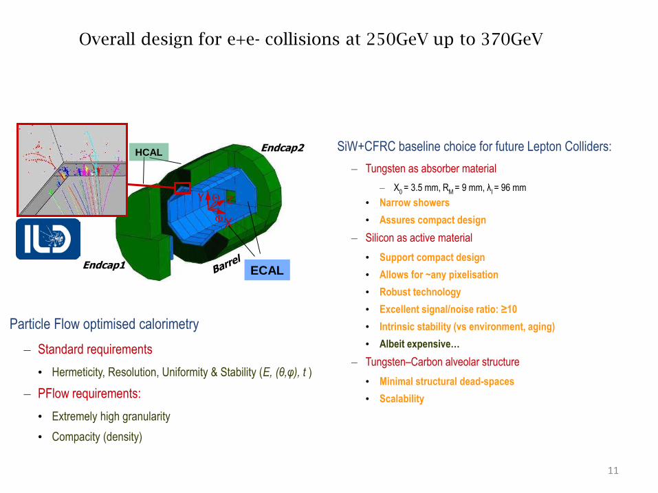
HCAL
ECAL
Endcap2
Endcap1
X
ZY
An Ultra-Granular SiW-ECAL for experiments
Particle Flow optimised calorimetry
– Standard requirements
• Hermeticity, Resolution, Uniformity & Stability (E, (θ,φ), t )
– PFlow requirements:
• Extremely high granularity
• Compacity (density)
SiW+CFRC baseline choice for future Lepton Colliders:
– Tungsten as absorber material
– X0 = 3.5 mm, R
M = 9 mm, λ
I= 96 mm
• Narrow showers
• Assures compact design
– Silicon as active material
• Support compact design
• Allows for ~any pixelisation
• Robust technology
• Excellent signal/noise ratio: ≥10
• Intrinsic stability (vs environment, aging)
• Albeit expensive…
– Tungsten–Carbon alveolar structure
• Minimal structural dead-spaces
• Scalability
Overall design for e+e- collisions at 250GeV up to 370GeV
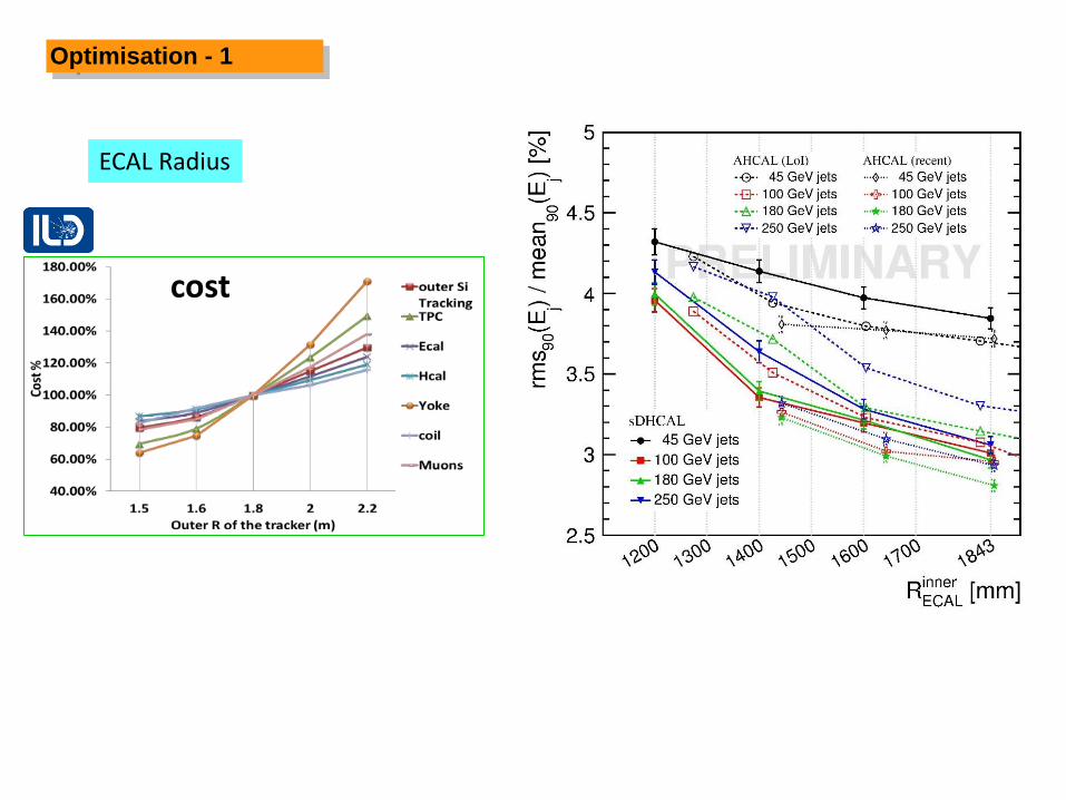
Optimisation - 1
cost
ECAL Radius
Reduced number of Layers
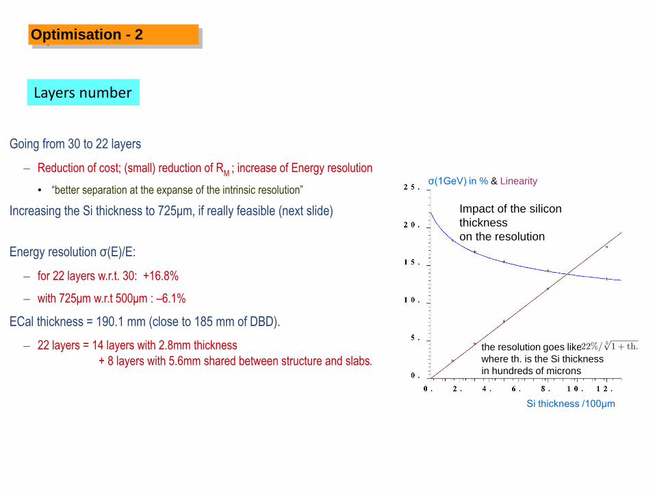
Going from 30 to 22 layers
– Reduction of cost; (small) reduction of RM
; increase of Energy resolution
• “better separation at the expanse of the intrinsic resolution”
Increasing the Si thickness to 725μm, if really feasible (next slide)
Energy resolution σ(E)/E:
– for 22 layers w.r.t. 30: +16.8%
– with 725μm w.r.t 500μm : –6.1%
ECal thickness = 190.1 mm (close to 185 mm of DBD).
– 22 layers = 14 layers with 2.8mm thickness
+ 8 layers with 5.6mm shared between structure and slabs.
Impact of the silicon
thickness
on the resolution
the resolution goes like
where th. is the Si thickness
in hundreds of microns
σ(1GeV) in % & Linearity
Si thickness /100μm
Optimisation - 2
Layers number
14
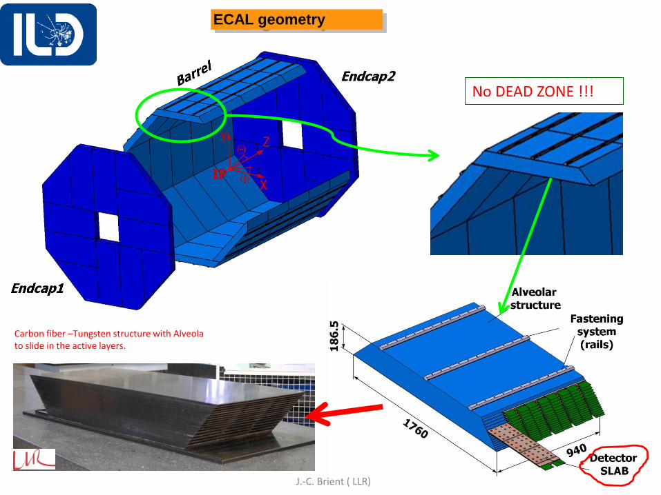
Carbon fiber –Tungsten structure with Alveolato slide in the active layers.
No DEAD ZONE !!!
J.-C. Brient ( LLR)
ECAL geometry
15
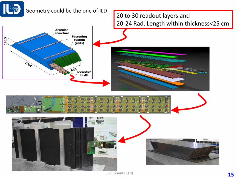
20 to 30 readout layers and 20-24 Rad. Length within thickness<25 cm
Geometry could be the one of ILD
J.-C. Brient ( LLR)
16
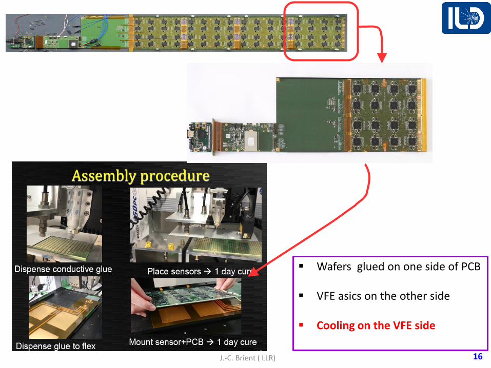
Wafers glued on one side of PCB
VFE asics on the other side
Cooling on the VFE side
J.-C. Brient ( LLR)
17
Silicon pad for ILD ECAL
Wafers glued on PCB
“Long slab”
Testing new slabs
in CERN SPS
Intensive study ongoing
mainly on electronics
of large scale
Sensor and readout
concept mature enough
Long-life needed: reliability is crucial
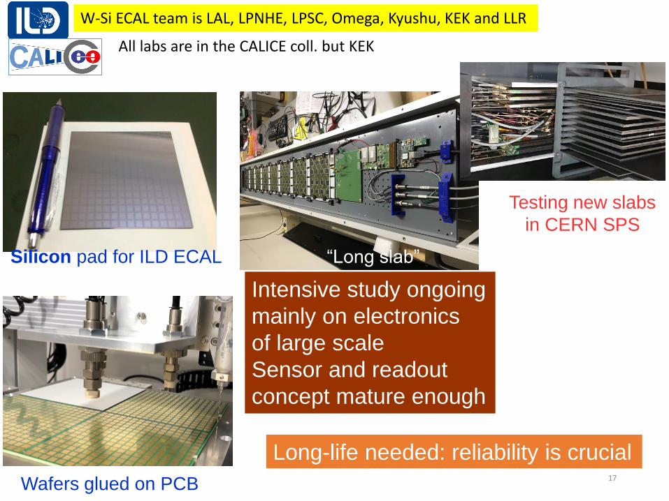
W-Si ECAL team is LAL, LPNHE, LPSC, Omega, Kyushu, KEK and LLR
All labs are in the CALICE coll. but KEK
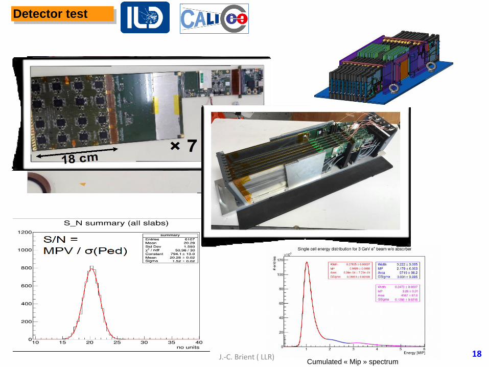
18Cumulated « Mip » spectrum
in 3GeV e-
J.-C. Brient ( LLR)
Detector test
19
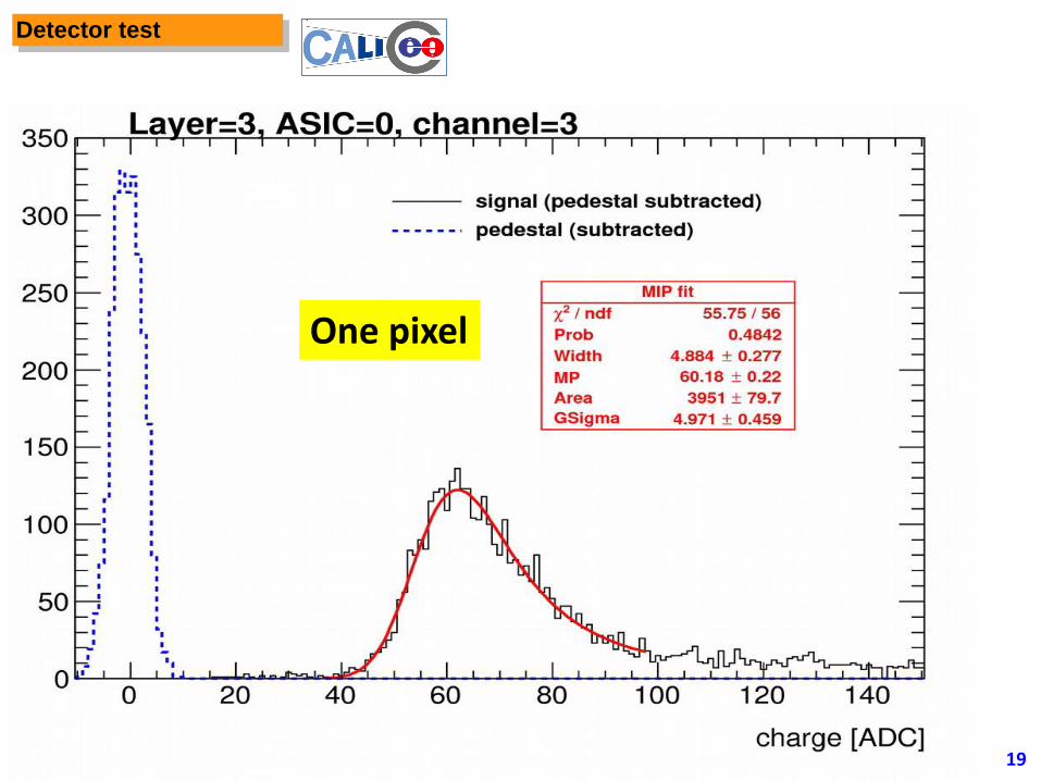
Detector test
One pixel
20
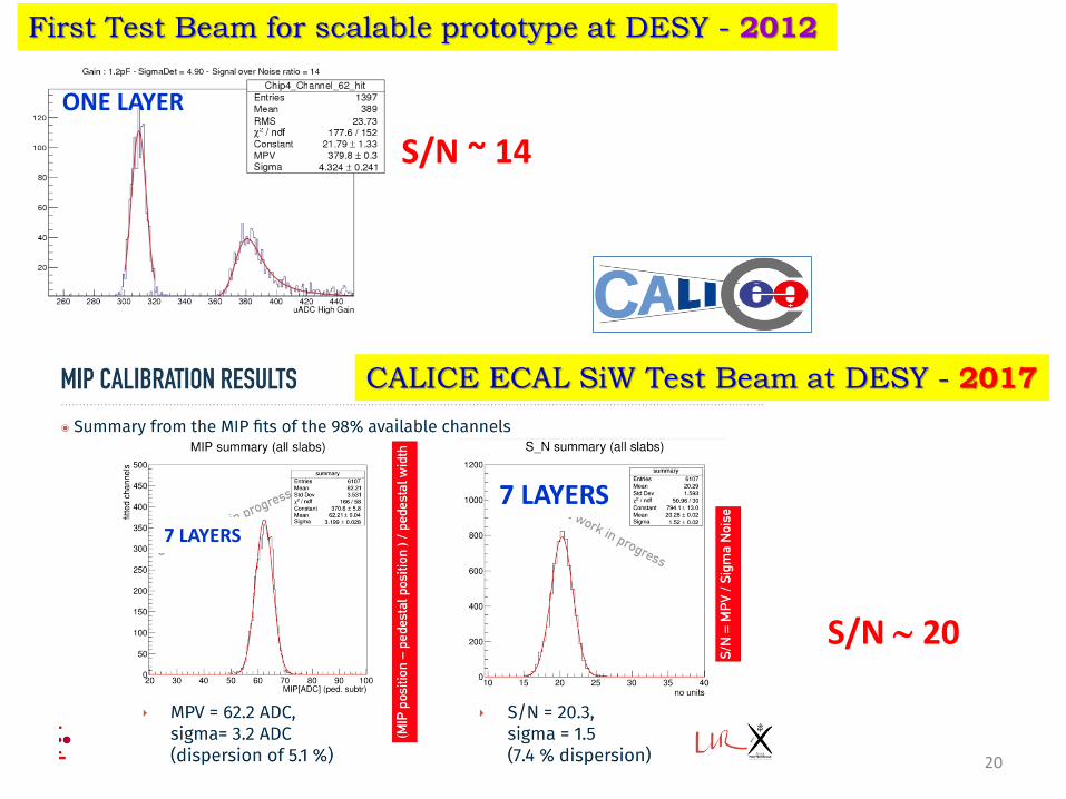
CALICE ECAL SiW Test Beam at DESY - 2017
First Test Beam for scalable prototype at DESY - 2012
S/N ~ 14
S/N 20
ONE LAYER
7 LAYERS
7 LAYERS
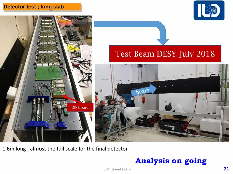
21
DIF board
Test Beam DESY July 2018
Analysis on goingJ.-C. Brient ( LLR)
1.6m long , almost the full scale for the final detector
Detector test ; long slab
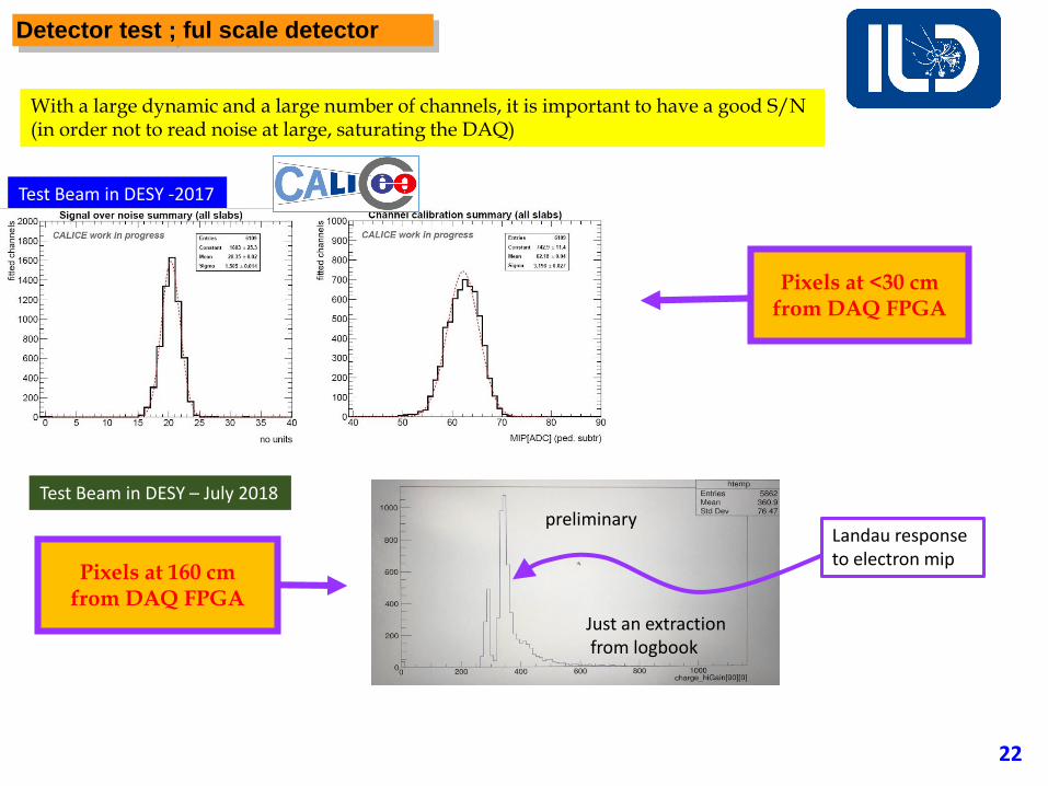
22
Test Beam in DESY -2017
With a large dynamic and a large number of channels, it is important to have a good S/N(in order not to read noise at large, saturating the DAQ)
Cut at 0.5 mip
Test Beam in DESY – July 2018
Pixels at <30 cm from DAQ FPGA
Pixels at 160 cm from DAQ FPGA
Landau response to electron mip
preliminary
Just an extractionfrom logbook
Detector test ; ful scale detector
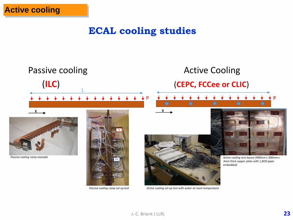
23
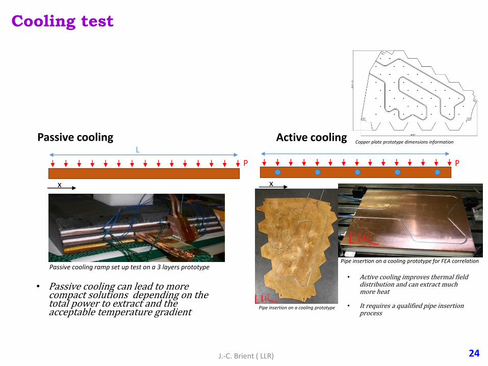
Passive cooling Active Cooling
(ILC) (CEPC, FCCee or CLIC)
P
x
L
x
P
Passive cooling ramp example
Passive cooling ramp set up test
Active cooling test layout (400mm x 300mm x 3mm thick copper plate with 1,8OD pipes embedded)
Active cooling set up test with water at room temperature
J.-C. Brient ( LLR)
ECAL cooling studies
Active cooling
Active coolingPassive cooling
P
x
L
x
• Passive cooling can lead to more compact solutions depending on the total power to extract and the acceptable temperature gradient
• Active cooling improves thermal field distribution and can extract much more heat
• It requires a qualified pipe insertion process
P
Passive cooling ramp set up test on a 3 layers prototype
Pipe insertion on a cooling prototype
Copper plate prototype dimensions information
Pipe insertion on a cooling prototype for FEA correlation
Cooling test
24J.-C. Brient ( LLR)
P
x
L
x
P
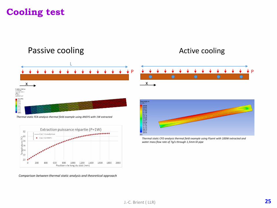
Thermal static FEA analysis thermal field example using ANSYS with 1W extracted
Comparison between thermal static analysis and theoretical approach
Thermal static CFD analysis thermal field example using Fluent with 100W extracted and water mass flow rate of 7g/s through 1,5mm ID pipe
Passive cooling Active cooling
Cooling test
25J.-C. Brient ( LLR)
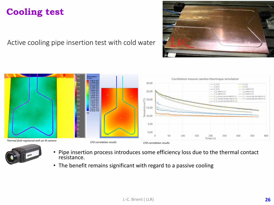
Active cooling pipe insertion test with cold water
• Pipe insertion process introduces some efficiency loss due to the thermal contact resistance.
• The benefit remains significant with regard to a passive cooling
Thermal field registered with an IR cameraCFD correlation results CFD correlation results
Cooling test
J.-C. Brient ( LLR) 26
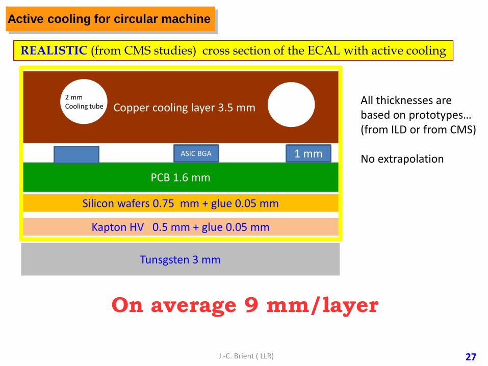
REALISTIC (from CMS studies) cross section of the ECAL with active cooling
27
Silicon wafers 0.75 mm + glue 0.05 mm
PCB 1.6 mm
Tunsgsten 3 mm
ASIC BGA 1 mm
Kapton HV 0.5 mm + glue 0.05 mm
Copper cooling layer 3.5 mm2 mmCooling tube
On average 9 mm/layer
J.-C. Brient ( LLR)
All thicknesses are based on prototypes…(from ILD or from CMS)
No extrapolation
Active cooling for circular machine
28
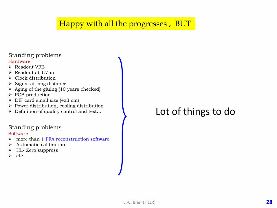
Standing problemsHardware
Readout VFE
Readout at 1.7 m
Clock distribution
Signal at long distance
Aging of the gluing (10 years checked)
PCB production
DIF card small size (4x3 cm)
Power distribution, cooling distribution
Definition of quality control and test…
Standing problemsSoftware
more than 1 PFA reconstruction software
Automatic calibration
HL- Zero suppress
etc…
Happy with all the progresses , BUT
Lot of things to do
J.-C. Brient ( LLR)

29
PFA possible only if (or more globally “jets”)
30
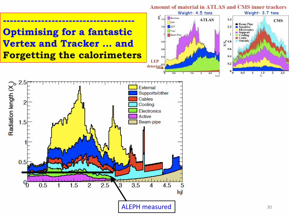
--------------------------------------
Optimising for a fantastic
Vertex and Tracker … and
Forgetting the calorimeters
ALEPH measured
31
The future ECALs are more cameras than thermometers
32
Why do we need 24X0 ?
Before you asked for questions, I have one for the audience
Instead to start from the hardware, I think the 2 detectors have to be optimized for different type of performances on physics results
Point 1
Point 2
Before to conclude
CONCLUSION
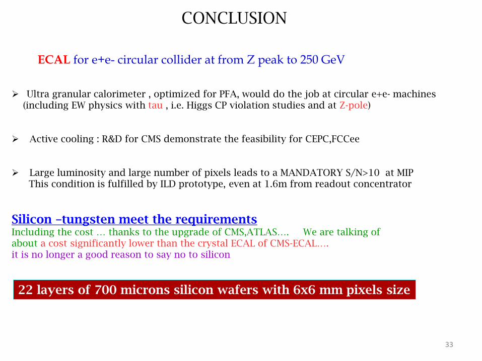
Ultra granular calorimeter , optimized for PFA, would do the job at circular e+e- machines(including EW physics with tau , i.e. Higgs CP violation studies and at Z-pole)
Active cooling : R&D for CMS demonstrate the feasibility for CEPC,FCCee
Large luminosity and large number of pixels leads to a MANDATORY S/N>10 at MIP This condition is fulfilled by ILD prototype, even at 1.6m from readout concentrator
Silicon –tungsten meet the requirementsIncluding the cost … thanks to the upgrade of CMS,ATLAS…. We are talking of about a cost significantly lower than the crystal ECAL of CMS-ECAL….it is no longer a good reason to say no to silicon
33
ECAL for e+e- circular collider at from Z peak to 250 GeV
22 layers of 700 microns silicon wafers with 6x6 mm pixels size

34
35
Full prototype with about 20 layers at the end of 2018 .. mid/end 2019
• Test Beam (Data taking and analysis) 2019-2020 (No beam at CERN, remains DESY (low energy) or FERMILAB)
• Going from ILC type to CEPC type. Cooling, pixels size, total rad. Length, etc…
• Going from prototype to “full scalable” (we have already 1.6m long detector slab)
• Interact with industry for optimized production and cost (tungsten, silicon, etc…)(amazing for me that HPK is the single producer in the world for high resistivity silicon
wafers)
Transfer knowledge to students about ultra-granular calorimeter(there is specific problems to this type of device…. Ask for to CMS / )Important to learn about with real hardware device… HGCAL can tell you
All groups interested , do not hesitate , contact us , there is work for all [email protected]
On the near and mid-term future
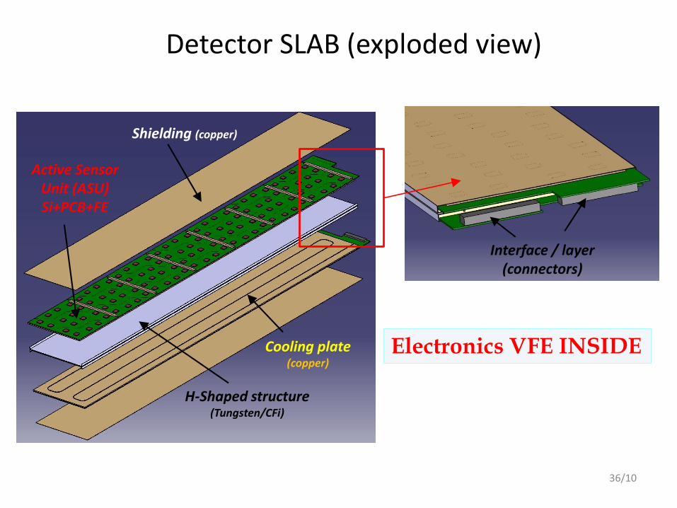
Detector SLAB (exploded view)
Active Sensor Unit (ASU)Si+PCB+FE
H-Shaped structure (Tungsten/CFi)
Shielding (copper)
Cooling plate (copper)
Interface / layer (connectors)
36/10
Electronics VFE INSIDE
37
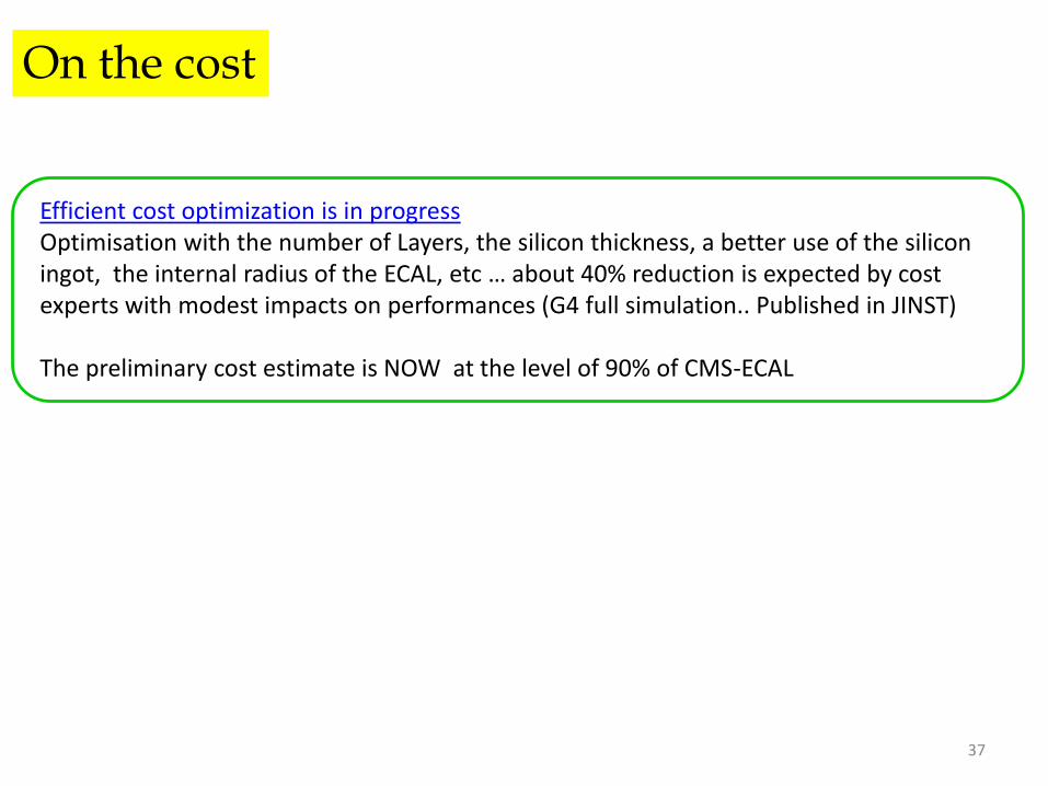
Efficient cost optimization is in progressOptimisation with the number of Layers, the silicon thickness, a better use of the silicon ingot, the internal radius of the ECAL, etc … about 40% reduction is expected by cost experts with modest impacts on performances (G4 full simulation.. Published in JINST)
The preliminary cost estimate is NOW at the level of 90% of CMS-ECAL
On the cost
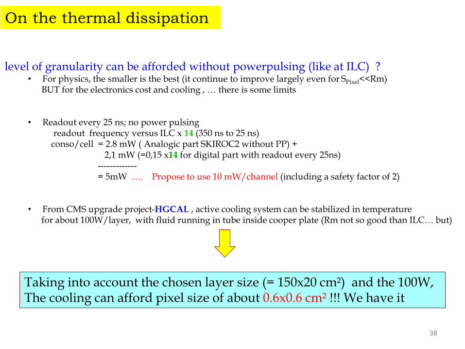
level of granularity can be afforded without powerpulsing (like at ILC) ?• For physics, the smaller is the best (it continue to improve largely even for SPixel<<Rm)
BUT for the electronics cost and cooling , … there is some limits
• Readout every 25 ns; no power pulsingreadout frequency versus ILC x 14 (350 ns to 25 ns) conso/cell = 2.8 mW ( Analogic part SKIROC2 without PP) +
2,1 mW (=0,15 x14 for digital part with readout every 25ns)-------------= 5mW …. Propose to use 10 mW/channel (including a safety factor of 2)
• From CMS upgrade project-HGCAL , active cooling system can be stabilized in temperature for about 100W/layer, with fluid running in tube inside cooper plate (Rm not so good than ILC… but)
Taking into account the chosen layer size (= 150x20 cm²) and the 100W, The cooling can afford pixel size of about 0.6x0.6 cm² !!! We have it
38
On the thermal dissipation
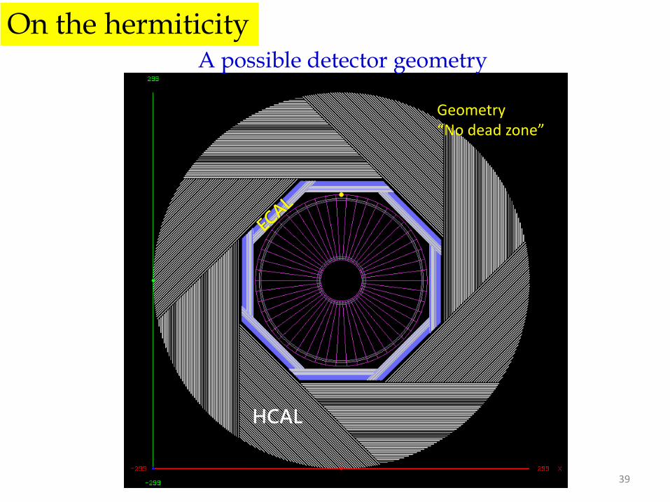
HCAL
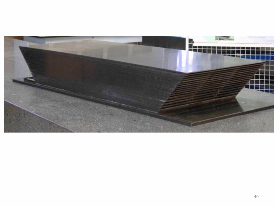
Geometry“No dead zone”
A possible detector geometry
39
On the hermiticity
40