Embed Size (px)
Citation preview
Silicon photonics is the merging of silicon electronic components, and photonics.
Silicon has revolutionized the electronics industry due to the following advantages:
•Ready Availability
•High Purification Levels
•Easy Manufacture
•Thermal and Mechanical Properties
•Resulting in Low cost
The electronics industry is finding limitations based on intrinsic properties in materials.
Examples: Speed limitations in interconnects
Communications expectation to increase speed decrease size
Photonics often provide an answer to these limitations although using past technology is not competitive fiscally. Creating photonics with silicon, promises the advent of a new low cost industry.
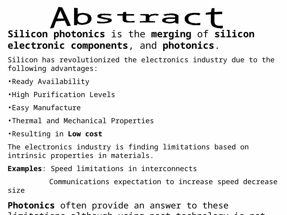
Demonstrating reality of Moore’s Law.
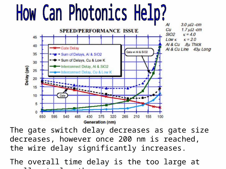
The gate switch delay decreases as gate size decreases, however once 200 nm is reached, the wire delay significantly increases.
The overall time delay is the too large at small gate lengths.
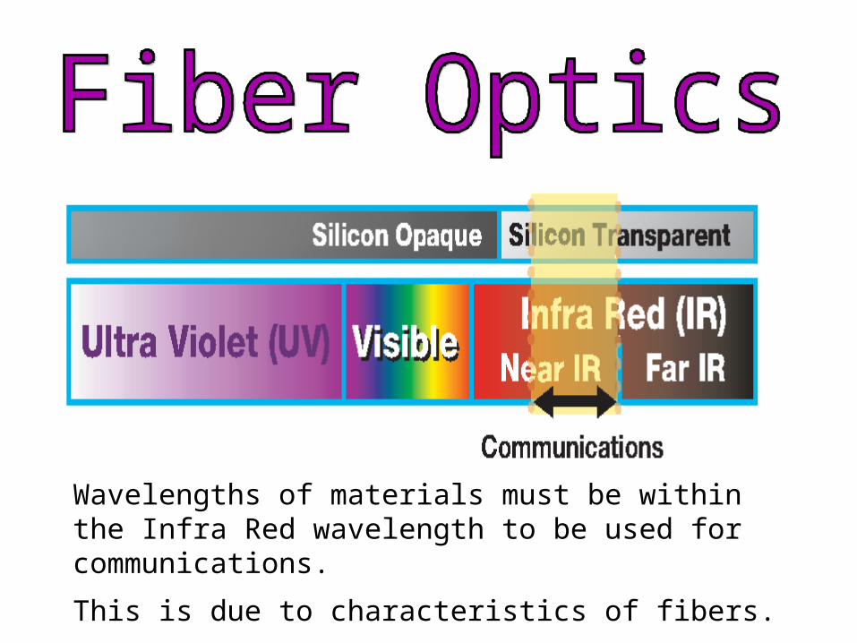
Wavelengths of materials must be within the Infra Red wavelength to be used for communications.
This is due to characteristics of fibers.
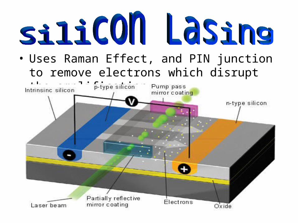
• Uses Raman Effect, and PIN junction to remove electrons which disrupt the amplification
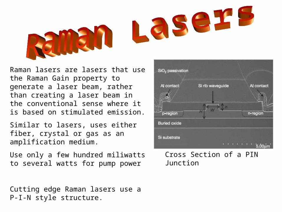
Raman lasers are lasers that use the Raman Gain property to generate a laser beam, rather than creating a laser beam in the conventional sense where it is based on stimulated emission.
Similar to lasers, uses either fiber, crystal or gas as an amplification medium.
Use only a few hundred miliwatts to several watts for pump power
Cutting edge Raman lasers use a P-I-N style structure.
Cross Section of a PIN Junction
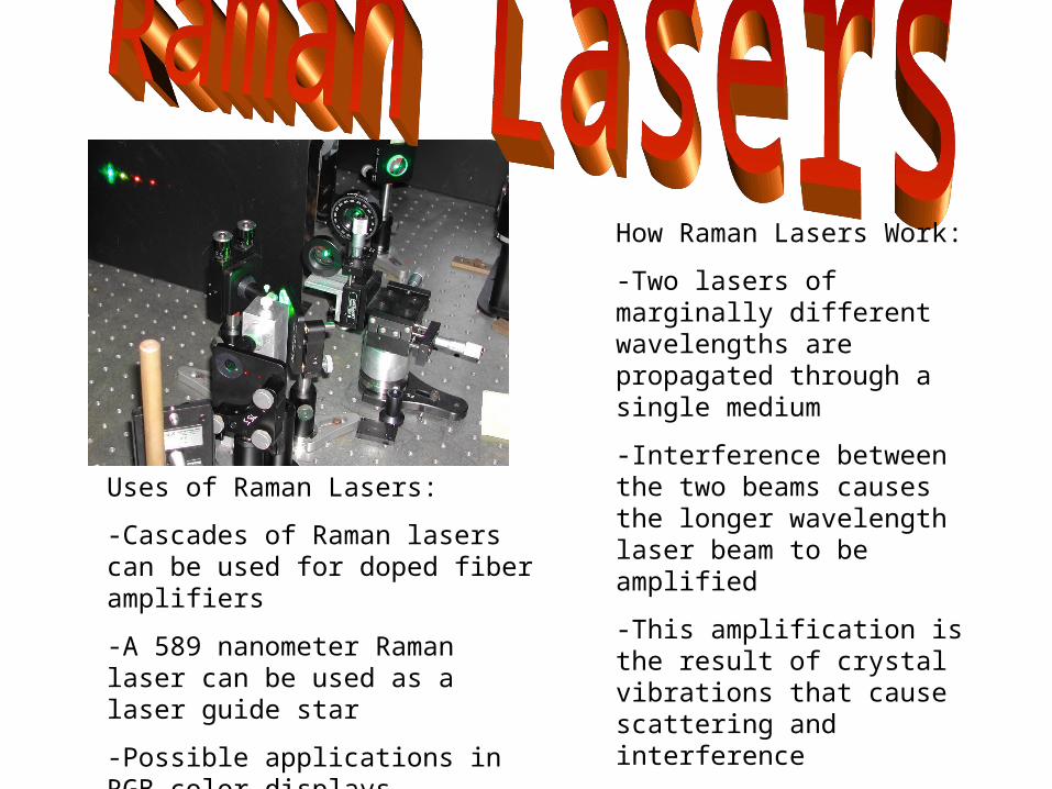
Uses of Raman Lasers:
-Cascades of Raman lasers can be used for doped fiber amplifiers
-A 589 nanometer Raman laser can be used as a laser guide star
-Possible applications in RGB color displays
How Raman Lasers Work:
-Two lasers of marginally different wavelengths are propagated through a single medium
-Interference between the two beams causes the longer wavelength laser beam to be amplified
-This amplification is the result of crystal vibrations that cause scattering and interference
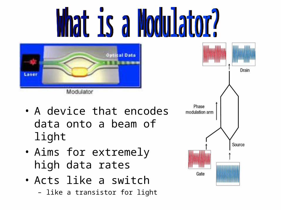
• A device that encodes data onto a beam of light
• Aims for extremely high data rates
• Acts like a switch – like a transistor for light
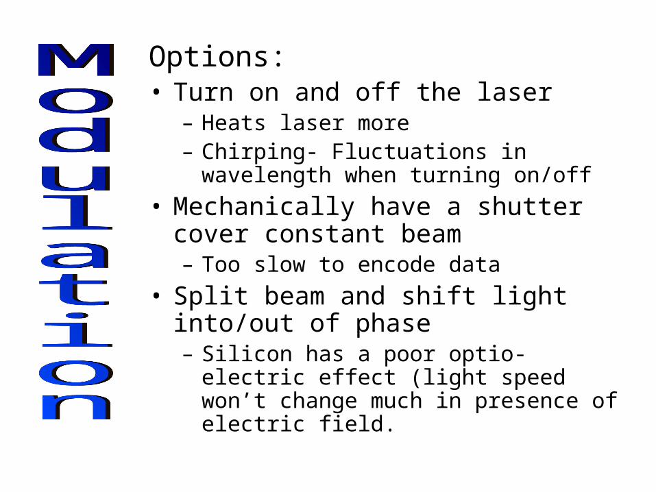
Options:• Turn on and off the laser
– Heats laser more– Chirping- Fluctuations in wavelength when
turning on/off
• Mechanically have a shutter cover constant beam– Too slow to encode data
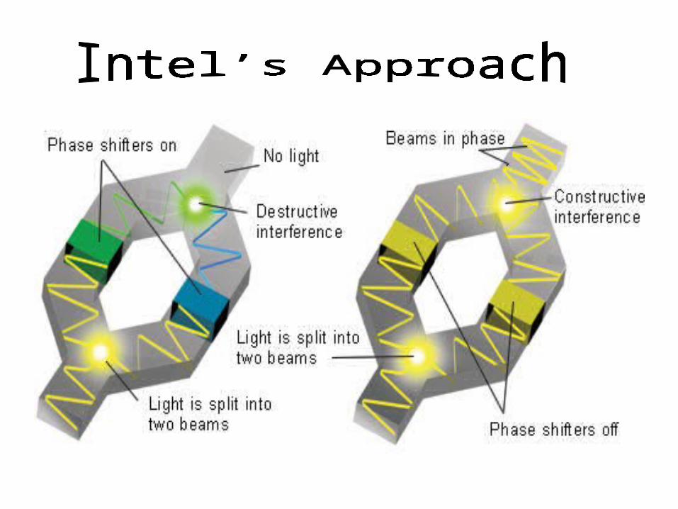
• Split beam and shift light into/out of phase– Silicon has a poor optio-electric effect (light
speed won’t change much in presence of electric field.
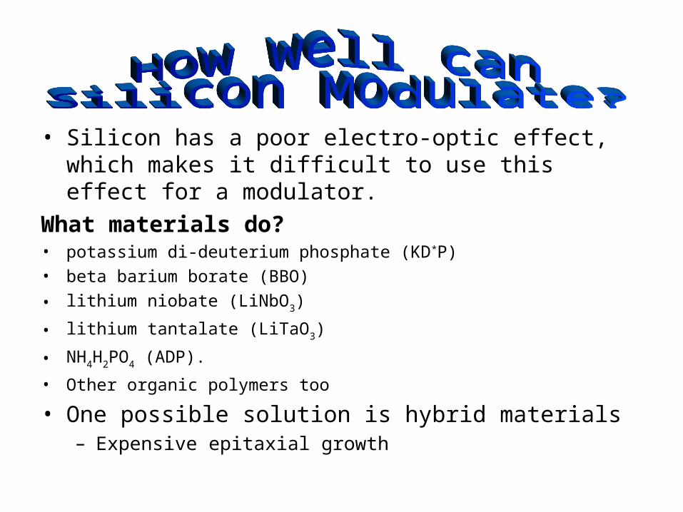
• Silicon has a poor electro-optic effect, which makes it difficult to use this effect for a modulator.
What materials do?• potassium di-deuterium phosphate (KD*P)
• beta barium borate (BBO)
• lithium niobate (LiNbO3)
• lithium tantalate (LiTaO3)
• NH4H2PO4 (ADP).
• Other organic polymers too
• One possible solution is hybrid materials– Expensive epitaxial growth
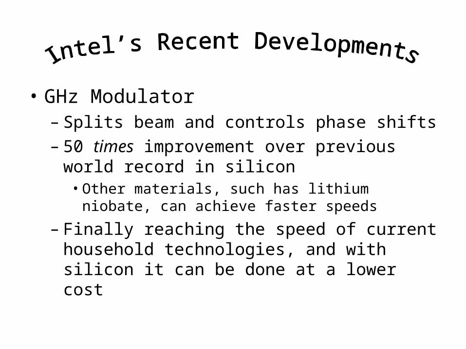
• GHz Modulator– Splits beam and controls phase shifts– 50 times improvement over previous world
record in silicon• Other materials, such has lithium niobate, can
achieve faster speeds
– Finally reaching the speed of current household technologies, and with silicon it can be done at a lower cost
• Uses the “free carrier plasma dispersion effect,” where charges in the waveguide change silicon’s index of refraction
• Previous techniques just injected the charge carriers, which slowly dissipate and thus limited speed.
• Intel used a transistor-like device to eject and remove the charge carriers to attain faster speeds.
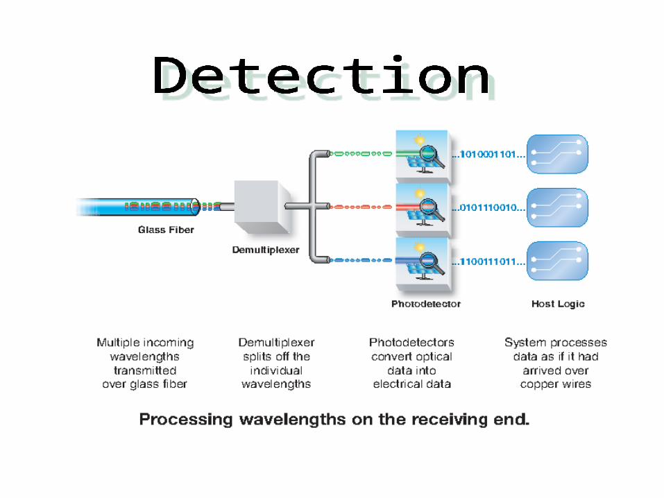
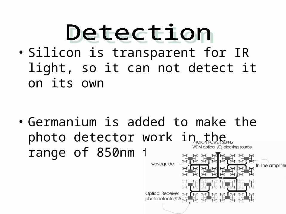
• Silicon is transparent for IR light, so it can not detect it on its own
• Germanium is added to make the photo detector work in the range of 850nm to 1310 nm
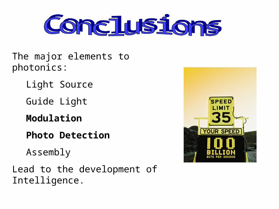
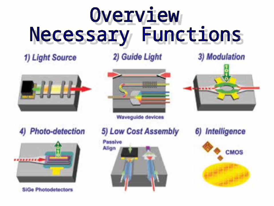
The major elements to photonics:
Light Source
Guide Light
Modulation
Photo Detection
Assembly
Lead to the development of Intelligence.
• http://www.intel.com/research/platform/sp/• ftp://download.intel.com/technology/silicon/sp/download/I
ntel_Advances_Silicon_Photonics.pdf• http://www.spectrum.ieee.org/print/1915• ftp://download.intel.com/technology/silicon/sp/download/
sipwp2.pdf• http://domino.research.ibm.com/comm/research_projects
.nsf/pages/photonics.projects.html• http://ej.iop.org/links/rtr01ul,v/yjb33FX32xG7bIHPav5vpA
/c326r1.pdf• http://www.rpphotonics.com/silicon_photonics.html• http://www.intel.com/technology/silicon/sp/glossary.htm
• http://www.intel.com/research/platform/sp/• ftp://download.intel.com/technology/silicon/sp/download/I
ntel_Advances_Silicon_Photonics.pdf• http://www.spectrum.ieee.org/print/1915• ftp://download.intel.com/technology/silicon/sp/download/
sipwp2.pdf• http://domino.research.ibm.com/comm/
research_projects.nsf/pages/photonics.projects.html• http://ej.iop.org/links/rtr01ul,v/
yjb33FX32xG7bIHPav5vpA/c326r1.pdf• http://www.rpphotonics.com/silicon_photonics.html• http://www.intel.com/technology/silicon/sp/glossary.htm