Embed Size (px)
Citation preview
Si5341, Si5340 Rev D Family ReferenceManual
Ultra Low Jitter, Any-Frequency, Any Output Clock Generator:Si5341, Si5340 Rev D Family Reference ManualThe Si5341/40 Clock Generators combine MultiSynth™ technologies to enable any-fre-quency clock generation for applications that require the highest level of jitter perform-ance. These devices are programmable via a serial interface with in-circuit programma-ble nonvolatile memory (NVM) ensuring power up with a known frequency configura-tion.
RELATED DOCUMENTS
• Si5341/0 Data Sheet• Si5341/0 Device Errata• Si5341/0 -EVB User Guide• Si5341/0 -EVB Schematics, BOM &
Layout• IBIS models
silabs.com | Building a more connected world. Rev. 1.1

Table of Contents1. Overview . . . . . . . . . . . . . . . . . . . . . . . . . . . . . . . . . 5
1.1 Work Flow Expectations with ClockBuilder Pro and the Register Map . . . . . . . . . . . 5
1.2 Family Product Comparison . . . . . . . . . . . . . . . . . . . . . . . . . 6
1.3 Available Software Tools and Support . . . . . . . . . . . . . . . . . . . . . . 7
2. Functional Description. . . . . . . . . . . . . . . . . . . . . . . . . . . . 82.1 Dividers . . . . . . . . . . . . . . . . . . . . . . . . . . . . . . . . 9
3. Powerup and Initialization . . . . . . . . . . . . . . . . . . . . . . . . . 123.1 Reset and Initialization . . . . . . . . . . . . . . . . . . . . . . . . . . .12
3.1.1 Power Supply Sequencing . . . . . . . . . . . . . . . . . . . . . . .12
3.2 NVM Programming . . . . . . . . . . . . . . . . . . . . . . . . . . . .13
4. Supply Voltage. . . . . . . . . . . . . . . . . . . . . . . . . . . . . . 14
5. Clock Inputs. . . . . . . . . . . . . . . . . . . . . . . . . . . . . . . 155.1 Inputs on XA/XB . . . . . . . . . . . . . . . . . . . . . . . . . . . . .15
5.1.1 Crystal on XA/XB. . . . . . . . . . . . . . . . . . . . . . . . . . .155.1.2 Clock Input on XA/XB . . . . . . . . . . . . . . . . . . . . . . . . .15
5.2 Clock Inputs on IN2, IN1, IN0. . . . . . . . . . . . . . . . . . . . . . . . .16
5.3 Reference Input Selection (IN0, IN1, IN2, XA/XB) . . . . . . . . . . . . . . . . . .17
5.4 Fault Monitoring . . . . . . . . . . . . . . . . . . . . . . . . . . . . .185.4.1 Status Indicators . . . . . . . . . . . . . . . . . . . . . . . . . . .195.4.2 Interrupt Pin (INTRb) . . . . . . . . . . . . . . . . . . . . . . . . .20
6. Output Clocks . . . . . . . . . . . . . . . . . . . . . . . . . . . . . . 216.1 Outputs . . . . . . . . . . . . . . . . . . . . . . . . . . . . . . . .21
6.2 Performance Guidelines for Outputs . . . . . . . . . . . . . . . . . . . . . .21
6.3 Output Signal Format . . . . . . . . . . . . . . . . . . . . . . . . . . .226.3.1 Differential Output Terminations. . . . . . . . . . . . . . . . . . . . . .236.3.2 Differential Amplitude Controls . . . . . . . . . . . . . . . . . . . . . .236.3.3 Output Driver Settings for LVPECL, LVDS, HCSL, and CML . . . . . . . . . . . .246.3.4 LVCMOS Output Terminations . . . . . . . . . . . . . . . . . . . . . .256.3.5 LVCMOS Output Impedance and Drive Strength Selection. . . . . . . . . . . . .266.3.6 LVCMOS Output Signal Swing . . . . . . . . . . . . . . . . . . . . . .266.3.7 LVCMOS Output Polarity . . . . . . . . . . . . . . . . . . . . . . . .276.3.8 Output Enable/Disable . . . . . . . . . . . . . . . . . . . . . . . . .286.3.9 Output Driver State When Disabled . . . . . . . . . . . . . . . . . . . .296.3.10 Synchronous/Asynchronous Output Disable Feature . . . . . . . . . . . . . .296.3.11 Output Delay Control (Δt0 – Δt4) . . . . . . . . . . . . . . . . . . . . .306.3.12 Sync Pin (Synchronizing R Dividers) . . . . . . . . . . . . . . . . . . . .31
6.4 Output Crosspoint . . . . . . . . . . . . . . . . . . . . . . . . . . . .31
6.5 Zero Delay Mode . . . . . . . . . . . . . . . . . . . . . . . . . . . . .31
silabs.com | Building a more connected world. Rev. 1.1 | 2

7. Digitally Controlled Oscillator (DCO) Modes . . . . . . . . . . . . . . . . . . . 327.1 Using the N Dividers for DCO Applications . . . . . . . . . . . . . . . . . . . .32
7.1.1 DCO with Frequency Increment/Decrement Pins/Bits . . . . . . . . . . . . . .327.1.2 DCO with Direct Register Writes . . . . . . . . . . . . . . . . . . . . .32
7.2 Using the M Divider for DCO Applications . . . . . . . . . . . . . . . . . . . .32
8. Dynamic PLL Changes . . . . . . . . . . . . . . . . . . . . . . . . . . . 338.1 Revisions B and A . . . . . . . . . . . . . . . . . . . . . . . . . . . .33
8.2 Revision D . . . . . . . . . . . . . . . . . . . . . . . . . . . . . . .33
8.3 Dynamic Changes to Output Frequencies without Changing PLL Settings. . . . . . . . . .34
8.4 Dynamic Changes to Output Frequencies while Changing PLL Settings Using a CBPro Register Map. . . . . . . . . . . . . . . . . . . . . . . . . . . . . . . . . . .34
9. Serial Interface . . . . . . . . . . . . . . . . . . . . . . . . . . . . . . 35
9.1 I2C Interface . . . . . . . . . . . . . . . . . . . . . . . . . . . . . .36
9.2 SPI Interface . . . . . . . . . . . . . . . . . . . . . . . . . . . . . .38
10. Field Programming. . . . . . . . . . . . . . . . . . . . . . . . . . . . 42
11. Recommended Crystals and External Oscillators . . . . . . . . . . . . . . . . 43
12. Crystal and Device Circuit Layout Recommendations . . . . . . . . . . . . . .4412.1 64-Pin QFN Si5341 Layout Recommendations . . . . . . . . . . . . . . . . . .44
12.1.1 Si5341 Applications without a Crystal . . . . . . . . . . . . . . . . . . .4412.1.2 Si5341 Crystal Layout Guidelines . . . . . . . . . . . . . . . . . . . . .4512.1.3 Output Clocks . . . . . . . . . . . . . . . . . . . . . . . . . . .49
12.2 44-Pin QFN Si5340 Layout Recommendations . . . . . . . . . . . . . . . . . .5012.2.1 Si5340 Applications without a Crystal as the Reference Clock . . . . . . . . . . .5012.2.2 Si5340 Crystal Guidelines . . . . . . . . . . . . . . . . . . . . . . .51
13. Power Management . . . . . . . . . . . . . . . . . . . . . . . . . . . 5413.1 Power Management Features . . . . . . . . . . . . . . . . . . . . . . . .54
13.2 Power Supply Recommendations . . . . . . . . . . . . . . . . . . . . . . .54
13.3 Grounding Vias . . . . . . . . . . . . . . . . . . . . . . . . . . . . .54
13.4 Power Supply Sequencing . . . . . . . . . . . . . . . . . . . . . . . . .55
14. Base vs. Factory Preprogrammed Devices . . . . . . . . . . . . . . . . . . . 5614.1 “Base” Devices (Also Known as “Blank” Devices) . . . . . . . . . . . . . . . . .56
14.2 Factory Preprogrammed (Custom OPN) Devices . . . . . . . . . . . . . . . . .56
15. Register Map . . . . . . . . . . . . . . . . . . . . . . . . . . . . . . 5715.1 Register Map Overview and Default Settings Values . . . . . . . . . . . . . . . .57
15.2 Si5341 Register Map . . . . . . . . . . . . . . . . . . . . . . . . . . .5715.2.1 Page 0 Registers Si5341. . . . . . . . . . . . . . . . . . . . . . . .5815.2.2 Page 1 Registers Si5341. . . . . . . . . . . . . . . . . . . . . . . .6715.2.3 Page 2 Registers Si5341. . . . . . . . . . . . . . . . . . . . . . . .7115.2.4 Page 3 Registers Si5341. . . . . . . . . . . . . . . . . . . . . . . .77
silabs.com | Building a more connected world. Rev. 1.1 | 3

15.2.5 Page 9 Registers Si5341. . . . . . . . . . . . . . . . . . . . . . . .8115.2.6 Page A Registers Si5341 . . . . . . . . . . . . . . . . . . . . . . .8215.2.7 Page B Registers Si5341 . . . . . . . . . . . . . . . . . . . . . . .82
15.3 Si5340 Registers . . . . . . . . . . . . . . . . . . . . . . . . . . . .8315.3.1 Page 0 Registers Si5340. . . . . . . . . . . . . . . . . . . . . . . .8415.3.2 Page 1 Registers Si5340. . . . . . . . . . . . . . . . . . . . . . . .9315.3.3 Page 2 Registers Si5340. . . . . . . . . . . . . . . . . . . . . . . .9615.3.4 Page 3 Registers Si5340. . . . . . . . . . . . . . . . . . . . . . . 10215.3.5 Page 8 Registers Si5340. . . . . . . . . . . . . . . . . . . . . . . 10415.3.6 Page 9 Registers Si5340. . . . . . . . . . . . . . . . . . . . . . . 11315.3.7 Page A Registers Si5340 . . . . . . . . . . . . . . . . . . . . . .11415.3.8 Page B Registers Si5340 . . . . . . . . . . . . . . . . . . . . . .115
16. Appendix A—Setting the Differential Output Driver to Non-Standard Amplitudes . . . .117
17. Document Change List . . . . . . . . . . . . . . . . . . . . . . . . . .118
silabs.com | Building a more connected world. Rev. 1.1 | 4
1. Overview
Using patented MultiSynth™ technology, the Si5341/40 generates up to 10 unique clock frequencies, each with 0 ppm frequency syn-thesis error. Each output clock has an independent VDDO reference and selectable signal format, simplifying format/level translation.The loop filter is fully integrated on-chip eliminating the risk of potential noise coupling associated with discrete solutions.The Si5341/40is ideally suited for simplifying clock tree design by minimizing the number of timing components required. The Si5341/40 supports fac-tory or in-circuit programmable non-volatile memory, enabling the device to power up in a user-specified configuration. The default con-figuration may be overwritten at any time by reprogramming the device via I2C/SPI.
1.1 Work Flow Expectations with ClockBuilder Pro and the Register Map
This reference manual is to be used to describe all the functions and features of the parts in the product family with register map detailson how to implement them. It is important to understand that the intent is for customers to use the ClockBuilder Pro software to providethe initial configuration for the device. Although the register map is documented, all the details of the algorithms to implement a validfrequency plan are fairly complex and are beyond the scope of this document. Real-time changes to the frequency plan and other oper-ating settings are supported by the devices. However, describing all the possible changes are not a primary purpose of this document.Refer to Applications Notes and Knowledge Base article links within the ClockBuilder Pro GUI for information on how to implement themost common, real-time frequency plan changes.
The primary purpose of the software is that it saves having to understand all the complexities of the device. The software abstracts thedetails from the user to allow focus on the high level input and output configuration, making it intuitive to understand and configure forthe end application. The software walks the user through each step, with explanations about each configuration step in the process toexplain the different options available. The software will restrict the user from entering an invalid combination of selections. The finalconfiguration settings can be saved, written to an EVB and a custom part number can be created for customers who prefer to order afactory preprogrammed device. The final register maps can be exported to text files, and comparisons can be done by viewing the set-tings in the register map described in this document.
Si5341, Si5340 Rev D Family Reference ManualOverview
silabs.com | Building a more connected world. Rev. 1.1 | 5
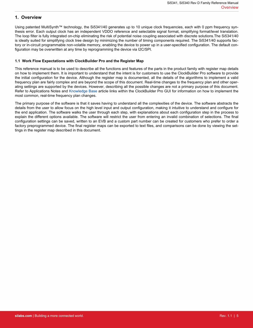
1.2 Family Product Comparison
The following table lists a comparison of the different family members.
Table 1.1. Product Selection Guide
Part Number Number of Inputs Number of Fractional Dividers Number of Outputs Package Type
Si5341 4 5 10 64-pin QFN
Si5340 4 4 4 44-pin QFN
Si5341/40
FB_IN
IN0
IN_SEL[1:0]
IN1
IN2
XB
XA
XTA
L
OSC
MultiSynth OUT0
OUT1
OUT2
OUT3
OUT4
OUT5
OUT6
OUT7
OUT8
OUT9
MultiSynth
MultiSynth
MultiSynth
MultiSynth
Si5340Si5341
PLL
NVM
I2C/ SPI
Control/Status
Figure 1.1. Block Diagram Si5341/40
Si5341, Si5340 Rev D Family Reference ManualOverview
silabs.com | Building a more connected world. Rev. 1.1 | 6

1.3 Available Software Tools and Support
ClockBuilder Pro is a software tool that is used for the Si5341/40 family and other product families, capable of configuring the timingchip in an intuitive friendly step by step process. The software abstracts the details from the user to allow focus on the high level inputand output configuration, making it intuitive to understand and configure for the end application. The software walks the user througheach step, with explanations about each configuration step in the process to explain the different options available. The software willrestrict the user from entering an invalid combination of selections. The final configuration settings can be saved, written to a device orwritten to the EVB and a custom part number can be created. ClockBuilder Pro integrates all the datasheets, application notes andinformation that might be helpful in one environment. It is intended that customers will use the software tool for the proper configurationof the device. Register map descriptions are given in the document should not be the only source of information for programming thedevice. The complexity of the algorithms is embedded in the software tool.
Si5341, Si5340 Rev D Family Reference ManualOverview
silabs.com | Building a more connected world. Rev. 1.1 | 7

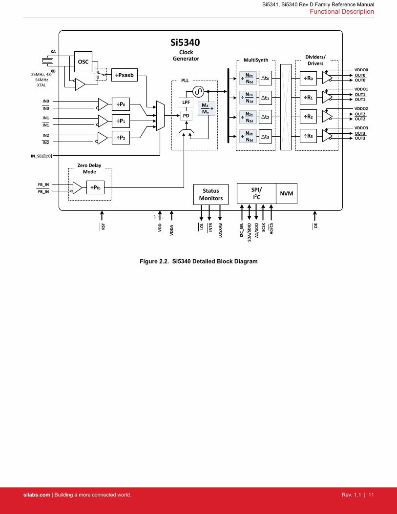
2. Functional Description
The Si5341/40 uses next generation MultiSynth™ technology to offer the industry’s most frequency-flexible, high performance clockgenerator. The PLL locks to either an external crystal (XA/XB) or to an external input on XAXB, IN0, IN1 or IN2. The input frequency(crystal or external input) is multiplied by the DSPLL and divided by the MultiSynth™ stage (N divider) and R divider to any frequency inthe range of 100 Hz to 712.5 MHz per output. The phase-locked loop is fully contained and does not require external loop filter compo-nents to operate. Its function is to phase lock to the selected input and provide a common reference to all the output MultiSynth high-performance fractional dividers (N). The high-resolution fractional MultiSynth™ dividers enables true any-frequency input to any-fre-quency on any of the outputs. A crosspoint mux connects any of the MultiSynth divided frequencies to any of the outputs drivers. Addi-tional output integer dividers (R) provide further frequency division if required. The frequency configuration of the device is programmedby setting the input dividers (P), the DSPLL feedback fractional divider (M_NUM/M_DEN), the MultiSynth fractional dividers (N_NUM/N_DEN), and the output integer dividers (R). Silicon Labs’ Clockbuilder Pro configuration utility determines the optimum divider valuesfor any desired input and output frequency plan.
The output drivers offer flexible output formats which are independently configurable on each of the outputs. This clock generator is fullyconfigurable via its serial interface (I2C/SPI) and includes in-circuit programmable non-volatile memory. The block diagram for theSi5341 is shown in Figure 2.1 Si5341 Detailed Block Diagram on page 10, and the block diagram for the Si5340 is shown in Figure2.2 Si5340 Detailed Block Diagram on page 11.
Si5341, Si5340 Rev D Family Reference ManualFunctional Description
silabs.com | Building a more connected world. Rev. 1.1 | 8

2.1 Dividers
There are five divider classes within the Si5341/40. See Figure 2.2 Si5340 Detailed Block Diagram on page 11 for a block diagramthat shows all of these dividers.• Wide range input dividers Pfb, P2, P1, P0
• Only integer divider values• Range is from 1 to 216 – 1• Since the input to the phase detector needs to be > 10 MHz, the practical range is limited to ~75 on the high side.• Each divider has an update bit that must be written to cause a newly written divider value to take effect.
• Narrow range input divider Pxaxb• Only divides by 1, 2, 4, 8
• Feedback M divider• Ultra low jitter in fractional and integer modes• MultiSynth divider• Integer or fractional divide values• 44 bit numerator, 32 bit denominator• Practical range limited by phase detector range of 10–120 MHz and VCO range of 13500–14256 MHz• This divider has an update bit that must be written to cause a newly written divider value to take effect.
• Output N dividers• Ultra low jitter in fractional and integer modes• MultiSynth divider• Integer or fractional divide values• 44 bit numerator, 32 bit denominator• Min value is 10• Maximum value is 212 – 1• Each N divider has an update bit that must be written to cause a newly written divider value to take effect. In addition there is a
global update bit that when written updates all N dividers.• Output R divider
• Only even integer divide values• Min value is 2• Maximum value is 225 – 2
Si5341, Si5340 Rev D Family Reference ManualFunctional Description
silabs.com | Building a more connected world. Rev. 1.1 | 9

VDD
VDDA
3
SDA/SDIOA1/SDO
SCLK
A0/CS
I2C_SEL
SPI/I2C NVM
RST
Zero Delay Mode
FB_IN
FB_IN
OE
Si5341Generator
Clock
÷R0
÷R2
÷R3
÷R4
÷R5
÷R6
÷R7
÷R8
÷R9
÷R1
OUT0
VDDO0OUT0
OUT2
VDDO2OUT2
OUT3
VDDO3OUT3
OUT4
VDDO4OUT4
OUT5
VDDO5OUT5
OUT6
VDDO6OUT6
OUT7
VDDO7OUT7
OUT8
VDDO8OUT8
OUT9
VDDO9OUT9
OUT1
VDDO1OUT1
÷Pfb
LPF
PD
÷ Mn
Md
PLL
IN_SEL[1:0]
XA
XB
25MHz, 48-54MHz XTAL
OSC
÷P2
÷P1
÷P0IN0
IN0
IN1
IN1
IN2
IN2
FDEC
FIN
C
Frequency Control
÷ N0n
N0dt0
÷ N2n
N2d
÷ N3n
N3d
÷ N4n
N4d
t2
t3
t4
÷ N1n
N1dt1
MultiSynth
SYN
C
Dividers/Drivers
StatusMonitors
LOL
INTR
÷Pxaxb
Figure 2.1. Si5341 Detailed Block Diagram
Si5341, Si5340 Rev D Family Reference ManualFunctional Description
silabs.com | Building a more connected world. Rev. 1.1 | 10
RST
OE
Si5340
÷ N0n
N0dt0
÷ N2n
N2d
÷ N3n
N3d
t2
t3
÷ N1n
N1dt1
IN_SEL[1:0]
XA
XB
IN0
IN0
IN1
IN1
IN2
IN2
LPF
PD
PLL
÷Mn
Md
Zero Delay Mode
FB_IN
FB_IN
LOL
INTR
LOSX
AB
SDA/
SDIO
A1/S
DOSC
LK
A0/C
S
I2C_
SEL
SPI/I2C NVMStatus
Monitors
GeneratorClock
÷P0
÷P1
÷P2
÷Pfb
MultiSynth
÷R0
÷R2
÷R3
÷R1
OUT0
VDDO0OUT0
OUT2
VDDO2OUT2
OUT3
VDDO3OUT3
OUT1
VDDO1OUT1
Dividers/Drivers
25MHz, 48-54MHz XTAL
OSC
÷Pxaxb
VDD
VDDA
3
Figure 2.2. Si5340 Detailed Block Diagram
Si5341, Si5340 Rev D Family Reference ManualFunctional Description
silabs.com | Building a more connected world. Rev. 1.1 | 11
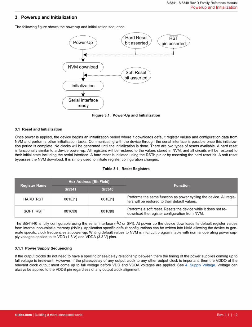
3. Powerup and Initialization
The following figure shows the powerup and initialization sequence.
Power-Up
Serial interface ready
RST pin asserted
Hard Reset bit asserted
Initialization
NVM downloadSoft Reset bit asserted
Figure 3.1. Power-Up and Initialization
3.1 Reset and Initialization
Once power is applied, the device begins an initialization period where it downloads default register values and configuration data fromNVM and performs other initialization tasks. Communicating with the device through the serial interface is possible once this initializa-tion period is complete. No clocks will be generated until the initialization is done. There are two types of resets available. A hard resetis functionally similar to a device power-up. All registers will be restored to the values stored in NVM, and all circuits will be restored totheir initial state including the serial interface. A hard reset is initiated using the RSTb pin or by asserting the hard reset bit. A soft resetbypasses the NVM download. It is simply used to initiate register configuration changes.
Table 3.1. Reset Registers
Register NameHex Address [Bit Field]
FunctionSi5341 Si5340
HARD_RST 001E[1] 001E[1] Performs the same function as power cycling the device. All regis-ters will be restored to their default values.
SOFT_RST 001C[0] 001C[0] Performs a soft reset. Resets the device while it does not re-download the register configuration from NVM.
The Si541/40 is fully configurable using the serial interface (I2C or SPI). At power up the device downloads its default register valuesfrom internal non-volatile memory (NVM). Application specific default configurations can be written into NVM allowing the device to gen-erate specific clock frequencies at power-up. Writing default values to NVM is in-circuit programmable with normal operating power sup-ply voltages applied to its VDD (1.8 V) and VDDA (3.3 V) pins.
3.1.1 Power Supply Sequencing
If the output clocks do not need to have a specific phase/delay relationship between them the timing of the power supplies coming up tofull voltage is irrelevant. However, if the phase/delay of any output clock to any other output clock is important, then the VDDO of therelevant clock output must come up to full voltage before VDD and VDDA voltages are applied. See 4. Supply Voltage. Voltage canalways be applied to the VDDS pin regardless of any output clock alignment.
Si5341, Si5340 Rev D Family Reference ManualPowerup and Initialization
silabs.com | Building a more connected world. Rev. 1.1 | 12
3.2 NVM Programming
Because the NVM can be written two times, it is important to configure the registers correctly before beginning the NVM programmingprocess. Once a new configuration has been written to NVM, the old configuration is no longer accessible. Note: In-circuit programmingis only supported over a temperature range of 0 to 80 °C.
The procedure for writing registers into NVM is as follows:1. Ensure the part is configured correctly before proceeding.2. Write 0xC7 to NVM_WRITE register.3. Wait until DEVICE_READY = 0x0F4. Set NVM_READ_BANK 0x00E4[0] = "1".5. Wait until DEVICE_READY = 0x0F.6. Steps 4 and 5 can be replaced by simply powering down and then powering up the device.
Table 3.2. NVM Programming Registers
Register Name Hex Address [Bit Field] Function
Si5340 Si5341
AC-TIVE_NVM_BANK
0x00E2[5:0] 0x00E2[5:0] Identifies the active NVM bank.
NVM_WRITE 0x00E3[7:0] 0x00E3[7:0] Initiates an NVM write when written with 0xC7.
NVM_READ_BANK 0x00E4[0] 0x00E4[0] Download register values with content stored in NVM.
DEVICE_READY 0x00FE[7:0] 0x00FE[7:0] Indicates that the device serial interface is ready to accept com-mands.
Note: Any attempt to read or write any register other than DEVICE_READY before DEVICE_READY reads as 0x0F may corrupt theNVM programming. Note that this includes writes to the PAGE register.
Si5341, Si5340 Rev D Family Reference ManualPowerup and Initialization
silabs.com | Building a more connected world. Rev. 1.1 | 13

4. Supply Voltage
Three classes of supply voltages exist:
VDD = 1.8 V + –5%
VDDA = 3.3 V + –5%
VDDO = 1.8/2.5/3.3 V + –5%
VDDS. A 1.0 µF cap is recommended for voltage bypass.
There is no requirement for power supply sequencing unless the output clocks are required to be aligned with each other or if the out-puts must have a specific delay relationship between them as defined by the Nx_DELAY bits. In this case, the VDDO of each clock thatneeds to be aligned must be powered up before VDD and VDDA. If output to output alignment is wanted but it is not possible to proper-ly sequence the power supplies then the output clocks can be aligned by asserting the SOFT_RST bit (register 0x001C[5]) or perform-ing a hard reset (also downloads the NVM again) by momentarily setting the RST pin low. VDDS has no effect upon the output clockalignment as it is only used to power the LOSXAXBB and LOLB status outputs.
Note: One may observe that when powering up the VDD = 1.8 V rail first, that the VDDA = 3.3 V rail will initially follow the 1.8 V rail.Likewise, if the VDDA rail is powered down first then it will not drop far below VDD until VDD itself is powered down. This is due to thepad I/O circuits which have large MOSFET switches to select the local supply from either the VDD or VDDA rails. These devices arerelatively large and yield a parasitic diode between VDD and VDDA. Please allow for both VDD and VDDA to power-up and power-down before measuring their respective voltages.
Si5341, Si5340 Rev D Family Reference ManualSupply Voltage
silabs.com | Building a more connected world. Rev. 1.1 | 14
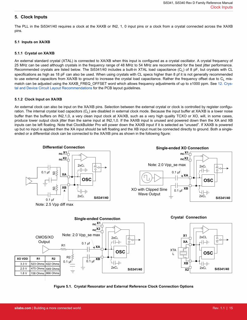
5. Clock Inputs
The PLL in the Si5341/40 requires a clock at the XAXB or IN2, 1, 0 input pins or a clock from a crystal connected across the XAXBpins.
5.1 Inputs on XA/XB
5.1.1 Crystal on XA/XB
An external standard crystal (XTAL) is connected to XA/XB when this input is configured as a crystal oscillator. A crystal frequency of25 MHz can be used although crystals in the frequency range of 48 MHz to 54 MHz are recommended for the best jitter performance.Recommended crystals are listed below. The Si5341/40 includes a built-in XTAL load capacitance (CL) of 8 pF, but crystals with CLspecifications as high as 18 pF can also be used. When using crystals with CL specs higher than 8 pf it is not generally recommendedto use external capacitors from XA/XB to ground to increase the crystal load capacitance. Rather the frequency offset due to CL mis-match can be adjusted using the XAXB_FREQ_OFFSET word which allows frequency adjustments of up to ±1000 ppm. See 12. Crys-tal and Device Circuit Layout Recommendations for the PCB layout guidelines.
5.1.2 Clock Input on XA/XB
An external clock can also be input on the XA/XB pins. Selection between the external crystal or clock is controlled by register configu-ration. The internal crystal load capacitors (CL) are disabled in external clock mode. Because the input buffer at XA/XB is a lower noisebuffer than the buffers on IN2,1,0, a very clean input clock at XA/XB, such as a very high quality TCXO or XO, will, in some cases,produce lower output clock jitter than the same input at IN2,1,0. If the XAXB input is unused and powered down then the XA and XBinputs can be left floating. Note that ClockBuilder Pro will power down the XAXB input if it is selected as “unused”. If XAXB is poweredup but no input is applied then the XA input should be left floating and the XB input must be connected directly to ground. Both a single-ended or a differential clock can be connected to the XA/XB pins as shown in the following figure:
50
Differential Connection
2xCL
2xCL
XB
XA
2xCL
2xCL
XB
XA
Single-ended XO Connection
Crystal Connection
OSC
XB
XA
XTAL
2xCL
2xCL
Si5341/40
Si5341/40 Si5341/40
Note: 2.0 Vpp_se max
XO with Clipped Sine Wave Output
2xCL
2xCL
XB
XAOSC
Si5341/40
Note: 2.0 Vpp_se maxCMOS/XO Output
R2
R1
XO VDD R1 R2
3.3 V 523 Ohms 2.5 V1.8 V
50
0.1 µf
0.1 µf
0.1 µf
0.1 µf
0.1 µf
0.1 µf0.1 µf
Single-ended Connection
Note: 2.5 Vpp diff max
X1
X2nc
nc
X1
X2ncnc
X1
X2nc
nc
X2
X1
OSCOSC
475 Ohms
158 Ohms
422 Ohms
649 Ohms 866 Ohms
Figure 5.1. Crystal Resonator and External Reference Clock Connection Options
Si5341, Si5340 Rev D Family Reference ManualClock Inputs
silabs.com | Building a more connected world. Rev. 1.1 | 15

5.2 Clock Inputs on IN2, IN1, IN0
A single ended or differential clock may be input to the IN2, 1, 0 inputs as shown below. All input signals must be ac-coupled. When INx(x = 0, 1, 2) is unused and powered down the plus and minus input can be left floating. ClockBuilder Pro will power down any INx inputthat is selected as “unused.” If any INx is powered up but does not have any input signal then the plus input should be left floating andthe minus input should be directly connected to ground. If the plus input is left floating and the minus input is connected to ground with a4.7 kΩ or smaller resistor, then the INx can be powered up or down when it does not have an input. The recommended input termina-tion schemes are shown in the figure below. Unused inputs can be disabled by register configuration.
AC Coupled LVCMOS or Single Ended
50
3.3 V, 2.5 V, 1.8 V LVCMOS or Single
Ended Signal
INx
INx
AC Coupled Differential
INx
INx
50
50
50Differential
Driver LVDS, LVPECL, CML
50
Si5341/40
Si5341/40
0.1 µf
0.1 uf
0.1 µf
0.1 µf
0.1 µf
Figure 5.2. Terminations for Differential and Single-Ended Inputs
Si5341, Si5340 Rev D Family Reference ManualClock Inputs
silabs.com | Building a more connected world. Rev. 1.1 | 16
5.3 Reference Input Selection (IN0, IN1, IN2, XA/XB)
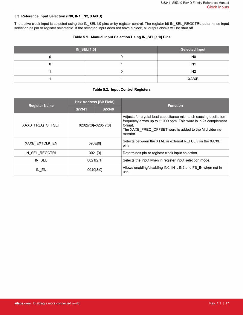
The active clock input is selected using the IN_SEL1,0 pins or by register control. The register bit IN_SEL_REGCTRL determines inputselection as pin or register selectable. If the selected input does not have a clock, all output clocks will be shut off.
Table 5.1. Manual Input Selection Using IN_SEL[1:0] Pins
IN_SEL[1:0] Selected Input
0 0 IN0
0 1 IN1
1 0 IN2
1 1 XA/XB
Table 5.2. Input Control Registers
Register NameHex Address [Bit Field]
FunctionSi5341 Si5340
XAXB_FREQ_OFFSET 0202[7:0]–0205[7:0]
Adjusts for crystal load capacitance mismatch causing oscillationfrequency errors up to ±1000 ppm. This word is in 2s complementformat. The XAXB_FREQ_OFFSET word is added to the M divider nu-merator.
XAXB_EXTCLK_EN 090E[0] Selects between the XTAL or external REFCLK on the XA/XBpins
IN_SEL_REGCTRL 0021[0] Determines pin or register clock input selection.
IN_SEL 0021[2:1] Selects the input when in register input selection mode.
IN_EN 0949[3:0] Allows enabling/disabling IN0, IN1, IN2 and FB_IN when not inuse.
Si5341, Si5340 Rev D Family Reference ManualClock Inputs
silabs.com | Building a more connected world. Rev. 1.1 | 17

5.4 Fault Monitoring
The Si5341/40 provides fault indicators which monitor loss of signal (LOS) of the inputs (IN0, IN1, IN2, XA/XB, FB_IN) and loss of lock(LOL) for the PLL. This is shown in the following figure.
PLLLPFPD
Mn
IN0
IN0LOS0÷P0
IN1
IN1÷P1
FB_INFB_IN
IN2
IN2÷P2
LOL
Si5341/40
XB
XA OSC
÷Pfb
Md÷
LOSXAXB
LOS1
LOS2
LOSFB
LOL
LOS0
LOS1
LOS2
LOSX
AB
INTR
÷Pxaxb
Figure 5.3. LOS and LOL Fault Monitors
Si5341, Si5340 Rev D Family Reference ManualClock Inputs
silabs.com | Building a more connected world. Rev. 1.1 | 18

5.4.1 Status Indicators
The state of the status monitors are accessible by reading registers through the serial interface or with dedicated pin (LOLb). Each ofthe status indicator register bits has a corresponding sticky bit (_FLG) in a separate register location. Once a status bit is asserted itscorresponding _FLG bit will remain asserted until cleared. Writing a logic zero to a _FLG register bit clears its state.
Table 5.3. Status Monitor Bits (Si5341 and Si5340)
Setting Name Hex Address [Bit Field] Function
Status Register Bits
SYSINCAL 0x000C[0] Asserted when in calibration.
LOSXAXB 0x000C[1]Loss of Signal at the XA input.
The Xb input does not have an LOS detector.
LOSREF 0x000C[2] Loss of Signal for the input that has been selected.
LOL 0x000C[3] Loss of Lock for the PLL.
SMBUS_TIMEOUT 0x000C[5] The SMB bus has a timeout.
LOSIN[3:0] 0x000D[3:0] Loss of Signal for the FB_IN, IN2, IN1, IN0 inputs.
Sticky Status Register Bits
SYSINCAL_FLG 0x0011[0] Sticky bit for SYSINCAL
LOSXAXB_FLG 0x0011[1] Sticky bit for LOSXAXBB
LOSREF_FLG 0x0011[2] Sticky bit for LOSREF
LOL_FLG 0x0011[3] Sticky bit for LOL
SMBUS_TIMEOUT_FLG 0x0011[5] Sticky bit for SMBUS_TIMEOUT
LOSIN_FLG 0x0012[3:0] Sticky bit for FB_IN, IN2, IN1, IN0
Si5341, Si5340 Rev D Family Reference ManualClock Inputs
silabs.com | Building a more connected world. Rev. 1.1 | 19

5.4.2 Interrupt Pin (INTRb)
An interrupt pin (INTRb) is asserted (low) whenever any of the unmasked _FLG bits are asserted. All _FLG bits are maskable to pre-vent assertion of the interrupt pin. The state of the INTRb pin is reset by writing zeros to all _FLG bits that are set or by writing a 1 tomask all _FLG bits that are set.
Table 5.4. Interrupt Mask Bits
Setting NameHex Address [Bit Field]
FunctionSi5341 and Si5342
SYSINCAL_INTR_MSK 0x0017[0] 1 = SYSINCAL_FLG is prevented from asserting the INTR pin
LOSXAXB_INTR_MSK 0x0017[1] 1 = LOSXAXB_FLG is prevented from asserting the INTR pin
LOSREF_INTR_MSK 0x0017[2] 1 = LOSREF_FLG is prevented from asserting the INTR pin
LOL_INTR_MSK 0x0017[3] 1 = LOL_FLG is prevented from asserting the INTR pin
SMB_TMOUT_INTR_MSK 0x0017[5] 1 = SMBUS_TIMEOUT_FLG is prevented from asserting the INTR pin
LOSIN _INTR_MSK[3:0] 0x0018[3:0] 1 = LOS_FLG is prevented from asserting the INTR pin
mask
mask
mask
mask
mask
maskLOL_FLG
LOSXAXB_FLG
LOSIN_FLG[3]
LOSIN_FLG[2]
LOSIN_FLG[1]
LOSIN_FLG[0]
INTRb
Figure 5.4. Interrupt Flags and Masks
Si5341, Si5340 Rev D Family Reference ManualClock Inputs
silabs.com | Building a more connected world. Rev. 1.1 | 20

6. Output Clocks
6.1 Outputs
The Si5341 supports ten differential output drivers which can be independently configured as differential or LVCMOS. The Si5340 sup-ports four output drivers independently configurable as differential or LVCMOS.
6.2 Performance Guidelines for Outputs
Whenever a number of high-frequency, fast-rise-time, large amplitude signals are all close to one another, the laws of physics dictatethat there will be some amount of crosstalk. The jitter of the Si5341/40 is so low that crosstalk can become a significant portion of thefinal measured output jitter. Some of the source of the crosstalk will be the Si5341/40, and some will be introduced by the PCB. It isdifficult (and possibly irrelevant) to allocate the jitter portions between these two sources because the jitter can only be measured whenan Si5341/40 is mounted on a PCB.
For extra fine tuning and optimization, in addition to following the usual PCB layout guidelines, crosstalk can be minimized by modifyingthe arrangements of different output clocks. For example, consider the following lineup of output clocks in the table below.
Table 6.1. Example of Output Clock Frequency Sequencing Choice
Output Not Recommended(Frequency MHz)
Recommended(Frequency MHz)
0 155.52 155.52
1 156.25 155.52
2 155.52 622.08
3 156.25 Not used
4 200 156.25
5 100 156.25
6 622.08 625
7 625 Not used
8 Not used 200
9 Not used 100
Using this example, a few guidelines are illustrated:1. Avoid adjacent frequency values that are close. A 155.52 MHz clock should not be next to a 156.25 MHz clock. If the jitter integra-
tion bandwidth goes up to 20 MHz, then keep adjacent frequencies at least 20 MHz apart.2. Adjacent frequency values that are integer multiples of one another are okay and these outputs should be grouped accordingly.
Noting that, because 155.52 x 4 = 622.08 and 156.25 x 4 = 625, it is acceptable to place 155.52 MHz close to 622.08 MHz and156.25 MHz close to 625 MHz.
3. Unused outputs can be used to separate clock outputs that might otherwise interfere with one another. In this case, see OUT3 andOUT7.
If some outputs have tight jitter requirements while others are relatively loose, rearrange the clock outputs so that the critical outputs arethe least susceptible to crosstalk. These guidelines typically only need to be followed by those applications that wish to achieve thehighest possible levels of jitter performance. Because CMOS outputs have large pk-pk swings and do not present a balanced load tothe VDDO supplies, CMOS outputs generate much more crosstalk than differential outputs. For this reason, CMOS outputs should beavoided whenever possible. When CMOS is unavoidable, even greater care must be taken with respect to the above guidelines. It ishighly recommended that you consult AN862: Optimizing Si534x Jitter Performance in Next Generation Internet Infrastructure Systems.
Si5341, Si5340 Rev D Family Reference ManualOutput Clocks
silabs.com | Building a more connected world. Rev. 1.1 | 21

6.3 Output Signal Format
The differential amplitude is fully programmable covering a wide variety of signal formats including LVDS, LVPECL, HCSL. For CML ornon-standard amplitude applications, see XREF Appendix A. The common-mode voltage must be set as required for LVDS or LVPECLor CML/non-standard amplitude levels. The differential formats can be either normal or low power. Low power format uses less powerfor the same amplitude but has the drawback of slower rise/fall times. The source impedance in low power format is much higher than100 ohms. See XREF Appendix A for register settings to implement variable amplitude differential outputs. In addition to supportingdifferential signals, any of the outputs can be configured as LVCMOS (3.3, 2.5, or 1.8 V) drivers providing up to 20 single-ended out-puts, or any combination of differential and single-ended outputs. Note also that CMOS output can create much more crosstalk thandifferential outputs so extra care must be taken in their pin replacement so that other clocks that need the lowest jitter are not on nearbypins. See AN862: Optimizing Si534x Jitter Performance in Next Generation Internet Infrastructure Systems for additional information.
Table 6.2. Output Signal Format Control Registers
Setting NameHex Address [Bit Field]
FunctionSi5341 Si5340
OUT0_FORMAT
OUT1_FORMAT
OUT2_FORMAT
OUT3_FORMAT
OUT4_FORMAT
OUT5_FORMAT
OUT6_FORMAT
OUT7_FORMAT
OUT8_FORMAT
OUT9_FORMAT
0109[2:0]
010E[2:0]
0113[2:0]
0118[2:0]
011D[2:0]
0122[2:0]
0127[2:0]
012C[2:0]
0131[2:0]
013B[2:0]
0113[2:0]
0118[2:0]
0127[2:0]
012C[2:0]
—
—
—
—
—
—
Selects the output signal format as normal differential, low powerdifferential, in phase CMOS, or complementary CMOS.
Si5341, Si5340 Rev D Family Reference ManualOutput Clocks
silabs.com | Building a more connected world. Rev. 1.1 | 22
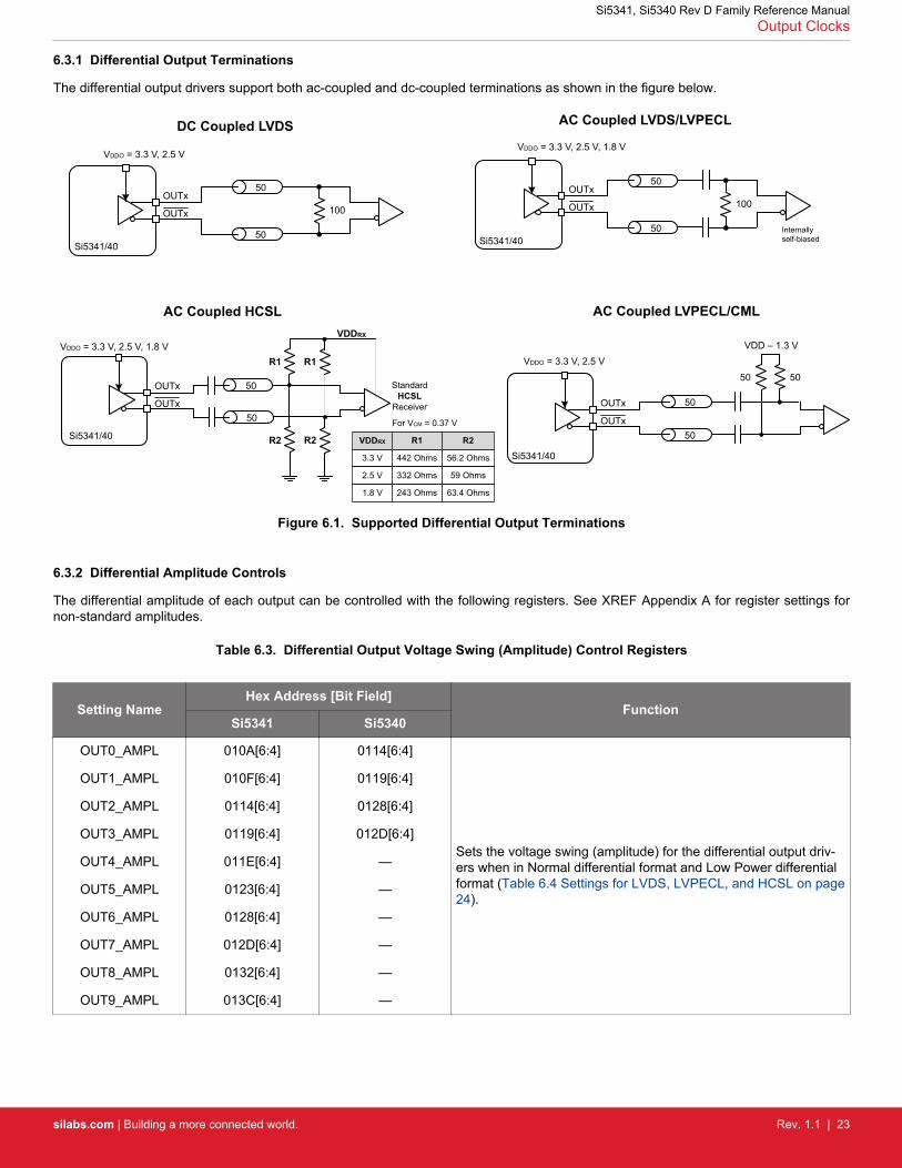
6.3.1 Differential Output Terminations
The differential output drivers support both ac-coupled and dc-coupled terminations as shown in the figure below.
100
50
50
Internally self-biased
AC Coupled LVDS/LVPECL
50
50
AC Coupled LVPECL/CML
VDD – 1.3 V
5050
50
50
100
DC Coupled LVDS
OUTx
OUTx
OUTx
OUTx
OUTx
OUTx
VDDO = 3.3 V, 2.5 V, 1.8 V
VDDO = 3.3 V, 2.5 V
VDDO = 3.3 V, 2.5 V
Si5341/40 Si5341/40
Si5341/40
VDDO = 3.3 V, 2.5 V, 1.8 V
AC Coupled HCSL
R1
OUTx
OUTx
Si5341/40
50
50
R1
R2 R2
VDDRX
StandardHCSL
Receiver
VDDRX R1 R2
3.3 V 442 Ohms 56.2 Ohms
2.5 V 332 Ohms 59 Ohms
1.8 V 243 Ohms 63.4 Ohms
For VCM = 0.37 V
Figure 6.1. Supported Differential Output Terminations
6.3.2 Differential Amplitude Controls
The differential amplitude of each output can be controlled with the following registers. See XREF Appendix A for register settings fornon-standard amplitudes.
Table 6.3. Differential Output Voltage Swing (Amplitude) Control Registers
Setting NameHex Address [Bit Field]
FunctionSi5341 Si5340
OUT0_AMPL
OUT1_AMPL
OUT2_AMPL
OUT3_AMPL
OUT4_AMPL
OUT5_AMPL
OUT6_AMPL
OUT7_AMPL
OUT8_AMPL
OUT9_AMPL
010A[6:4]
010F[6:4]
0114[6:4]
0119[6:4]
011E[6:4]
0123[6:4]
0128[6:4]
012D[6:4]
0132[6:4]
013C[6:4]
0114[6:4]
0119[6:4]
0128[6:4]
012D[6:4]
—
—
—
—
—
—
Sets the voltage swing (amplitude) for the differential output driv-ers when in Normal differential format and Low Power differentialformat (Table 6.4 Settings for LVDS, LVPECL, and HCSL on page24).
Si5341, Si5340 Rev D Family Reference ManualOutput Clocks
silabs.com | Building a more connected world. Rev. 1.1 | 23
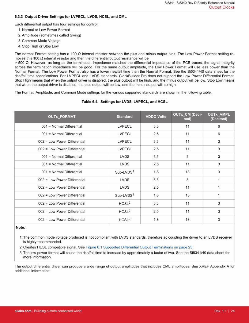
6.3.3 Output Driver Settings for LVPECL, LVDS, HCSL, and CML
Each differential output has four settings for control:1. Normal or Low Power Format2. Amplitude (sometimes called Swing)3. Common Mode Voltage4. Stop High or Stop Low
The normal Format setting has a 100 Ω internal resistor between the plus and minus output pins. The Low Power Format setting re-moves this 100 Ω internal resistor and then the differential output resistance will be > 500 Ω. However, as long as the termination impedance matches the differential impedance of the PCB traces, the signal integrityacross the termination impedance will be good. For the same output amplitude, the Low Power Format will use less power than theNormal Format. The Low Power Format also has a lower rise/fall time than the Normal Format. See the Si5341/40 data sheet for therise/fall time specifications. For LVPECL and LVDS standards, ClockBuilder Pro does not support the Low Power Differential Format.Stop High means that when the output driver is disabled, the plus output will be high, and the minus output will be low. Stop Low meansthat when the output driver is disabled, the plus output will be low, and the minus output will be high.
The Format, Amplitude, and Common Mode settings for the various supported standards are shown in the following table.
Table 6.4. Settings for LVDS, LVPECL, and HCSL
OUTx_FORMAT Standard VDDO Volts OUTx_CM (Deci-mal)
OUTx_AMPL(Decimal)
001 = Normal Differential LVPECL 3.3 11 6
001 = Normal Differential LVPECL 2.5 11 6
002 = Low Power Differential LVPECL 3.3 11 3
002 = Low Power Differential LVPECL 2.5 11 3
001 = Normal Differential LVDS 3.3 3 3
001 = Normal Differential LVDS 2.5 11 3
001 = Normal Differential Sub-LVDS1 1.8 13 3
002 = Low Power Differential LVDS 3.3 3 1
002 = Low Power Differential LVDS 2.5 11 1
002 = Low Power Differential Sub-LVDS1 1.8 13 1
002 = Low Power Differential HCSL2 3.3 11 3
002 = Low Power Differential HCSL2 2.5 11 3
002 = Low Power Differential HCSL2 1.8 13 3
Note:
1. The common mode voltage produced is not compliant with LVDS standards, therefore ac coupling the driver to an LVDS receiveris highly recommended.
2. Creates HCSL compatible signal. See Figure 6.1 Supported Differential Output Terminations on page 23.3. The low-power format will cause the rise/fall time to increase by approximately a factor of two. See the Si5341/40 data sheet for
more information.
The output differential driver can produce a wide range of output amplitudes that includes CML amplitudes. See XREF Appendix A foradditional information.
Si5341, Si5340 Rev D Family Reference ManualOutput Clocks
silabs.com | Building a more connected world. Rev. 1.1 | 24

6.3.4 LVCMOS Output Terminations
LVCMOS outputs are dc coupled as shown in the figure below.
3.3 V, 2.5 V, 1.8 V LVCMOSVDDO = 3.3 V, 2.5 V, 1.8 V
50Rs
50Rs
DC Coupled LVCMOS
OUTx
OUTx
Si5341/40
Figure 6.2. LVCMOS Output Terminations
Si5341, Si5340 Rev D Family Reference ManualOutput Clocks
silabs.com | Building a more connected world. Rev. 1.1 | 25

6.3.5 LVCMOS Output Impedance and Drive Strength Selection
Each LVCMOS driver has a configurable output impedance to accommodate different trace impedances and drive strengths. A sourcetermination resistor (Rs) is highly recommended to help match the selected output impedance to the trace impedance (i.e. Rs ~= TraceImpedance – Zs). For the best signal integrity, Silicon Labs strongly recommends using the setting that produces the lowest sourceimpedance and then choosing the proper external source resistor to produce the best signal shape at the end of the signal trace.
VDDO OUTx_CMOS_DRVValue Setting Source Impedance (ZS)
3.3 V
0x01 38 Ω
0x02 30 Ω
0x031 22 Ω
2.5 V
0x01 43 Ω
0x02 35 Ω
0x031 24 Ω
1.8 V0x02 46 Ω
0x031 31 Ω
Note:1. This setting is strongly recommended.
Table 6.5. LVCMOS Drive Strength Control Registers
Setting NameHex Address [Bit Field]
FunctionSi5341 Si5340
OUT0_CMOS_DRV
OUT1_CMOS_DRV
OUT2_CMOS_DRV
OUT3_CMOS_DRV
OUT4_CMOS_DRV
OUT5_CMOS_DRV
OUT6_CMOS_DRV
OUT7_CMOS_DRV
OUT8_CMOS_DRV
OUT9_CMOS_DRV
0109[7:6]
010E[7:6]
0113[7:6]
0118[7:6]
011D[7:6]
0122[7:6]
0127[7:6]
012C[7:6]
0131[7:6]
013B[7:6]
0113[7:6]
0118[7:6]
0127[7:6]
012C[7:6]
—
—
—
—
—
—
LVCMOS output impedance. See previous table.
6.3.6 LVCMOS Output Signal Swing
The signal swing (VOL/VOH) of the LVCMOS output drivers is set by the voltage on the VDDO pins. Each output driver has its ownVDDO pin allowing a unique output voltage swing for each of the LVCMOS drivers.
Si5341, Si5340 Rev D Family Reference ManualOutput Clocks
silabs.com | Building a more connected world. Rev. 1.1 | 26
6.3.7 LVCMOS Output Polarity
When a driver is configured as an LVCMOS output it generates a clock signal on both pins (OUTx and OUTxb). By default the clock onthe OUTxb pin is generated with the opposite polarity (complementary) with the clock on the OUTx pin. The polarity of these clocks isconfigurable enabling in-phase clock generation and/or inverted polarity with respect to other output drivers.
Table 6.6. LVCMOS Output Polarity Control Registers
Setting Name Hex Address [Bit Field] Function
Si5341 Si5340
OUT0_INV
OUT1_INV
OUT2_INV
OUT3_INV
OUT4_INV
OUT5_INV
OUT6_INV
OUT7_INV
OUT8_INV
OUT9_INV
010B[7:6]
0110[7:6]
0115[7:6]
011A[7:6]
011F[7:6]
0124[7:6]
0129[7:6]
012E[7:6]
0133[7:6]
0138[7:6]
0115[7:6]
011A[7:6]
0129[7:6]
012E[7:6]
—
—
—
—
—
—
Controls output polarity of the OUTx and OUTxb pins when inLVCMOS mode. Selections are as follows:
OUTx_INV OUTx OUTxb Comment
0 0 CLK CLK Both in phase(default)
0 1 CLK CLKb OUTxb inverted
1 0 CLKb CLKb OUTx and OUTxbinverted
1 1 CLKb CLK OUTx inverted
Si5341, Si5340 Rev D Family Reference ManualOutput Clocks
silabs.com | Building a more connected world. Rev. 1.1 | 27

6.3.8 Output Enable/Disable
Clock outputs are disabled by four signals within Si5341/40 and the OEB pin:• OUTALL_DISABLE_LOW• SYSINCAL• OUTx_OE• LOL• OEB pin
The following figure shows the logic of how these disable/enables occur.
Enable to IndividualOutput Drivers
LOL
SYSINCAL
OUTALL_DISABLE_LOW
OUTX_OE
OEB Pin
OUTX_OE are the individual Output Driver enables as shown in the table below
1 instance of this is used per output driver
Figure 6.3. Output Enable
Table 6.7. Output Enable/Disable Control Registers
Setting NameHex Address [Bit Field]
FunctionSi5341 Si5340
OUTALL_DISABLE_LOW 0102[0]0 = Disables all outputs.
1 = All outputs are not disabled by this signal but may be disabledby other signals or the OEB pin. See figure above.
OUT0_OE
OUT1_OE
OUT2_OE
OUT3_OE
OUT4_OE
OUT5_OE
OUT6_OE
OUT7_OE
OUT8_OE
OUT9_OE
0108[1]
010D[1]
0112[1]
0117[1]
011C[1]
0121[1]
0126[1]
012B[1]
0130[1]
013A[1]
0112[1]
0117[1]
0126[1]
012B[1]
—
—
—
—
—
—
0 = Specific output disabled.
1 = Specific output is not disabled. The OEB pin or other signalswithin the device may be causing an output disable. See figureabove.
Si5341, Si5340 Rev D Family Reference ManualOutput Clocks
silabs.com | Building a more connected world. Rev. 1.1 | 28

6.3.9 Output Driver State When Disabled
The disabled state of an output driver is configurable as: disable low, disable high, or disable mid. When set for disable mid, the outputcommon mode voltage will stay nearly the same when disabled as when enabled.
Table 6.8. Output Driver Disable State Control Registers
Setting NameHex Address [Bit Field]
FunctionSi5341 Si5340
OUT0_DIS_STATE
OUT1_DIS_STATE
OUT2_DIS_STATE
OUT3_DIS_STATE
OUT4_DIS_STATE
OUT5_DIS_STATE
OUT6_DIS_STATE
OUT7_DIS_STATE
OUT8_DIS_STATE
OUT9_DIS_STATE
0109[5:4]
010E[5:4]
0113[5:4]
0118[5:4]
011D[5:4]
0122[5:4]
0127[5:4]
012C[5:4]
0131[5:4]
013B[5:4]
0113[5:4]
0118[5:4]
0127[5:4]
012C[5:4]
—
—
—
—
—
—
Determines the state of an output driver when disabled. Selecta-ble as:• Disable logic low.• Disable logic high
6.3.10 Synchronous/Asynchronous Output Disable Feature
Outputs can be configured to disable synchronously or asynchronously. In synchronous disable mode the output will wait until a clockperiod has completed before the driver is disabled. This prevents unwanted runt pulses from occurring when disabling an output. Inasynchronous disable mode the output clock will disable immediately without waiting for the period to complete.
Table 6.9. Synchronous Disable Control Registers
Setting NameHex Address [Bit Field]
FunctionSi5341 Si5340
OUT0_SYNC_EN
OUT1_SYNC_EN
OUT2_SYNC_EN
OUT3_SYNC_EN
OUT4_SYNC_EN
OUT5_SYNC_EN
OUT6_SYNC_EN
OUT7_SYNC_EN
OUT8_SYNC_EN
OUT9_SYNC_EN
0109[3]
010E[3]
0113[3]
0118[3]
011D[3]
0122[3]
0127[3]
012C[3]
0131[3]
013B[3]
0113[3]
0118[3]
0127[3]
012C[3]
—
—
—
—
—
—
When this bit is high, the output will turn on/off (enable/disable)without generating runt pulses or glitches. The default for this bitis high. When this bit is low, the outputs will turn on/off asynchro-nously. In this case, there may be glitches on the output when itturns on/off.
Si5341, Si5340 Rev D Family Reference ManualOutput Clocks
silabs.com | Building a more connected world. Rev. 1.1 | 29

6.3.11 Output Delay Control (Δt0 – Δt4)
The Si5341/40 uses independent MultiSynth dividers (N0 – N4) to generate up to five unique frequencies to its 10 outputs through acrosspoint switch. By default, all clocks are phase aligned. A delay path (Δt0 – Δt4) associated with each of these dividers is availablefor applications that need a specific output skew configuration. This is useful for PCB trace length mismatch compensation. Theresolution of the phase adjustment is 1/(256 x FVCO) seconds (FVCO in Hz) per step definable in a range of ±32768/(256 x FVCO) (FVCOin Hz). The output delay controls (Dt0–Dt4) are register configurable. After the delay controls are configured, the soft reset bit,SOFT_RST, must be set high.
÷N0 t0
÷N1 t1
÷N2 t2
÷N3 t3
÷N4 t4
OUT2
VDDO2OUT2
VDDO3
÷R2
OUT3OUT3÷R3
OUT1
VDDO1OUT1÷R1
OUT5
VDDO5OUT5
VDDO6
÷R5
OUT6OUT6÷R6
OUT4
VDDO4OUT4÷R4
OUT7
VDDO7OUT7
VDDO8
÷R7
OUT8OUT8÷R8
OUT0
VDDO0OUT0÷R0
VDDO9
OUT9OUT9÷R9
Figure 6.4. Example of Independently-Configurable Path Delays
All delay values are restored to their NVM programmed values after power-up or after a hard reset. Delay default values can be writtento the NVM allowing a custom delay offset configuration at power-up or after a hardware reset.
Here is an example:
If FVCO = 13.75 GHz and the desired delay is 3 ns and the desired output clock is connected to N0, then the N0_DELAY would becalculated as the N0_DELAY = 3–9 x 256 x 13.759 = 10,560 decimal = 2940 hex.
Table 6.10. Delay Registers
Setting NameHex Address [Bit Field]
FunctionSi5341 Si5340
N0_DELAY 0359[7:0] - 035A[7:0]Configures path delay values for each N divider. For example,N0_DELAY is [0x035A[7:0] 0x0359[7:0]]. Each 16-bit number is2s complement. The output delay is Nx_DELAY/ (256 x FVCO)where FVCO is the frequency of the VCO in Hz, and the delay is inseconds. Note that the Si5340 does not have N4_DELAY.
N1_DELAY 035B[7:0] - 035C[7:0]
N2_DELAY 035D[7:0] - 035E[7:0]
N3_DELAY 035F[7:0] - 0360[7:0]
N4_DELAY 0361[7:0] - 0362[7:0]
Si5341, Si5340 Rev D Family Reference ManualOutput Clocks
silabs.com | Building a more connected world. Rev. 1.1 | 30

6.3.12 Sync Pin (Synchronizing R Dividers)
All the output R dividers are reset to the default NVM register state after a power-up or a hard reset. This ensures consistent and re-peatable phase alignment across all output drivers. Resetting the device using the RSTb pin or asserting the hard reset bit will have thesame result. The SYNCb pin provides another method of realigning the R dividers without resetting the device. This pin is positive edgetriggered. Asserting the sync register bit provides the same function. Note that using the SYNCb bit/pin guarantees that the outputs willalign to within 50 ns.
6.4 Output Crosspoint
The output crosspoint allows any of the N dividers to connect to any of the R dividers and output drivers. Note that each output driverhas a specific R divider that is permanently attached and has the same subscript in the name, i.e., R3 and OUT3.
Table 6.11. Output Crosspoint Control Registers
Setting NameHex Address [Bit Field]
FunctionSi5341 Si5340
OUT0_MUX_SEL
OUT1_MUX_SEL
OUT2_MUX_SEL
OUT3_MUX_SEL
OUT4_MUX_SEL
OUT5_MUX_SEL
OUT6_MUX_SEL
OUT7_MUX_SEL
OUT8_MUX_SEL
OUT9_MUX_SEL
010B[2:0]
0110[2:0]
0115[2:0]
011A[2:0]
011F[2:0]
0124[2:0]
0129[2:0]
012E[2:0]
0133[2:0]
013D[2:0]
0115[2:0]
011A[2:0]
0129[2:0]
012E[2:0]
—
—
—
—
—
—
Connects the output drivers to one of the N dividers. Selectionsare N0, N1, N2, N3, and N4 for each output divider.
6.5 Zero Delay Mode
Please contact Silicon Labs for support of this feature.
Si5341, Si5340 Rev D Family Reference ManualOutput Clocks
silabs.com | Building a more connected world. Rev. 1.1 | 31

7. Digitally Controlled Oscillator (DCO) Modes
An output that is controlled as a DCO is useful for simple tasks such as frequency margining, CPU speed control, or just changing theoutput frequency. The output can also be used for more sophisticated tasks such as FIFO management by adjusting the frequency ofthe read or write clock to the FIFO or using the output as a variable Local Oscillator in a radio application.
7.1 Using the N Dividers for DCO Applications
The N dividers can be digitally controlled to so that all outputs connected to the N divider change frequency in real time without anytransition glitches. There are two ways to control the N divider to accomplish this task:• Use the Frequency Increment/Decrement Pins or register bits.• Write directly to the numerator or denominator of the N divider.
The output N divider can be changed from its minimum value of 10 to its maximum value of 4095 in very small fractional increments ora single very large increment. Each N divider has a value of Nx_NUM/Nx_DEN. Nx_NUM is a 44 bit word and Nx_DEN is a 32 bit word.Clockbuilder Pro left shifts these values as far as possible before writing them to the actual Nx_NUM and Nx_DEN registers. For exam-ple, an integer Nx divider of 30/1, when left shifted, becomes Nx_NUM = 6442509440 (decimal) and Nx_DEN = 2147483648 (decimal).By adjusting the size of the Nx_NUM and Nx_DEN but keeping the ratio the same, the resolution of the LSbit of numerator or denomi-nator can be controlled.
When changing the N divider(s) to fractional values, the setting name N_PIBYP[4:0] must be a 0 for the N divider that is being changed.This applies when using FINC/FDEC or when directly writing to the N divider.
7.1.1 DCO with Frequency Increment/Decrement Pins/Bits
The FSTEPW (Frequency STEP Word) is a 44 bit word that is used to change the value of the Nx_NUM word. Whenever an FINC orFDEC is asserted, the FSTEPW will automatically add or subtract from the Nx_NUM word so that the output frequency will increment(FINC) or decrement (FDEC) respectively.
Each of the N dividers can be independently stepped up or down in numerical predefined steps with a maximum resolution that variesfrom ~ 0.05 ppb to a ~0.004 ppb depending upon the frequency plan. One or more N dividers can be controlled by FINC/FDEC at thesame time by use of the N_FSTEP_MSK bits. Any N divider that is masked by its corresponding bit in the N_FSTEP_MSK field will notchange when FINC or FDEC is asserted. The magnitude of the frequency change caused by FINC or FDEC is determined by the valueof the FSTEPW word and the magnitude of the word in Nx_NUM. For a specific frequency step size it may be necessary to adjust theNx_NUM value while keeping the ratio of Nx_NUM/Nx_DEN the same. When the FINC or FDEC pin or register bit is asserted the se-lected N dividers will have their numerator changed by the addition or subtraction of the Nx_FSTEPW so that an FINC will increase theoutput frequency and an FDEC will decrease the output frequency. An FINC or FDEC can be followed by another FINC or FDEC in 1µs minimum.
Because the output frequency = FVCO * Nx_DEN/(Rx * Nx_NUM), subsequent changes to Nx_NUM by the FSTEPW will not produceexactly the same output frequency change. The amount of error in the frequency step is extremely small and in a vast number of appli-cations will not cause a problem. When consecutive frequency steps must be exactly the same, it is possible to set FINC and FDEC tochange the Nx_DEN instead of Nx_NUM and then consecutive FINCs or FDECs will be exactly the same frequency change. However,there are some special setups that are necessary to achieve this. For more information contact Silicon Labs.
7.1.2 DCO with Direct Register Writes
When a N divider numerator (Nx_NUM) and its corresponding update bit (Nx_UPDATE) is written, the new numerator value will takeeffect and the output frequency will change without any glitches. The N divider numerator and denominator terms (Nx_NUM andNx_DEN) can be left and right shifted so that the least significant bit of the numerator word represents the exact step resolution that isneeded for your application. Each N divider has an update bit (Nx_UPDATE) that must be written to cause the written values to takeeffect. All N dividers can be updated at the same time by writing the N_UPDATE_ALL bit. Note that writing this bit will not cause anyoutput glitching on an N divider that did not have its numerator or denominator changed.
When changing the N divider denominator (Nx_DEN) it is remotely possible that a small phase change of ~550 fs may occur at theexact time of the frequency change. However with the proper setup it is possible to change Nx_DEN and never have a phase change. Ifyour application requires changing an N divider denominator, contact Silicon Labs.
7.2 Using the M Divider for DCO Applications
The VCO can be treated as a DCO by changing the value of the M feedback divider. By changing the M divider, all the output frequen-cies will change by the same amount in ppm. Changing the M divider is only valid for small changes in the output frequencies. ContactSilicon Labs for assistance in the implementation of this capability.
Si5341, Si5340 Rev D Family Reference ManualDigitally Controlled Oscillator (DCO) Modes
silabs.com | Building a more connected world. Rev. 1.1 | 32

8. Dynamic PLL Changes
8.1 Revisions B and A
It is possible for a PLL to become unresponsive (i.e., lose lock indefinitely) when it is dynamically reprogrammed or changed via theserial port. Reprogramming/changing the N divider does not affect the PLL. Any change that causes the VCO frequency to change bymore than 250 ppm since Power-up, NVM download, or SOFT_RST requires the following special sequence of writes. Changes to thefollowing registers require the following special sequence of writes:• XAXB_FREQ_OFFSET• PXAXB• MXAXB_NUM• MXAXB_DEN• M_NUM• M_DEN
1. First, the preamble:
Write 0x0B24 = 0xD8
Write 0x0B25 = 0x00
Write 0x0502 = 0x01
Write 0x0505 = 0x03
Write 0x0957 = 0x17
Write 0x0B4E = 0x1A2. Wait 300 ms.3. Then, perform the desired register modifications.4. Write SOFT_RST - 0x001C[0] = 15. Write the post-amble:
Write 0x0B24 = 0xDB
Write 0x0B25 = 0x02
8.2 Revision D
The Revision D preamble and postamble values for updating certain registers during device operation have changed after Revision B.Either the new or old values below may be written to Revision D or later devices without issue. No system software changes are neces-sary for legacy systems. When writing old values, note that reading back these registers will not give the written old values, but willreflect the new values. Silicon Labs recommends using the new values for all Revision D and later designs, since the write and readvalues will match.
The device revision can be determined in the setting DEVICE_REV, register 0x0005.
DEVICE_REV = 0x02 or higher: New Values
Revision D Preamble: 0x0B24 = 0xC0, 0x0B25 = 0x00
Revision D Postamble: 0x0B24 = 0xC3, 0x0B25 = 0x02
Note that revision B and earlier devices must continue to use the original values for these registers:
DEVICE_REV = 0x00 or 0x01: Old Values
Revision B Preamble: 0x0B24 = 0xD8, 0x0B25 = 0x00
Revision B Postamble: 0x0B24 = 0xDB, 0x0B25 = 0x02
Si5341, Si5340 Rev D Family Reference ManualDynamic PLL Changes
silabs.com | Building a more connected world. Rev. 1.1 | 33

8.3 Dynamic Changes to Output Frequencies without Changing PLL Settings
This section applies to the following scenario:1. A CBPro generated register map "was" used to program either the volatile or the non-volatile memory of a Si5340/1. Changes to
output frequencies without changing the PLL settings are desired.2. The CBPro project file can be used to look for the VCO frequency (FVCO), Ry, Nx values for each OUTy in the design report
and/or the datasheet addendum.
OUTy = FVCO/(Nx * Ry)
Solve for Nx based on the desired OUTy. The Nx dividers can be digitally controlled to so that all outputs connected to the Nx dividerchange frequency in real time without any transition glitches. There are two ways to control the Nx divider to accomplish this task:
1. Use the Frequency Increment/Decrement Pins or register bits.2. Write directly to the numerator or denominator of the Nx divider.
The details of both methods are covered in 7.1 Using the N Dividers for DCO Applications.
8.4 Dynamic Changes to Output Frequencies while Changing PLL Settings Using a CBPro Register Map
This section applies to the following scenario:1. A CBPro generated register map "is" used to program either the voltatile or the non-volatile memory of a Si5340/1.2. This needs a register write sequence provided in the CBPro export section as shown below.
Figure 8.1. CBPro Register Write Sequence While Changing PLL Settings
Si5341, Si5340 Rev D Family Reference ManualDynamic PLL Changes
silabs.com | Building a more connected world. Rev. 1.1 | 34
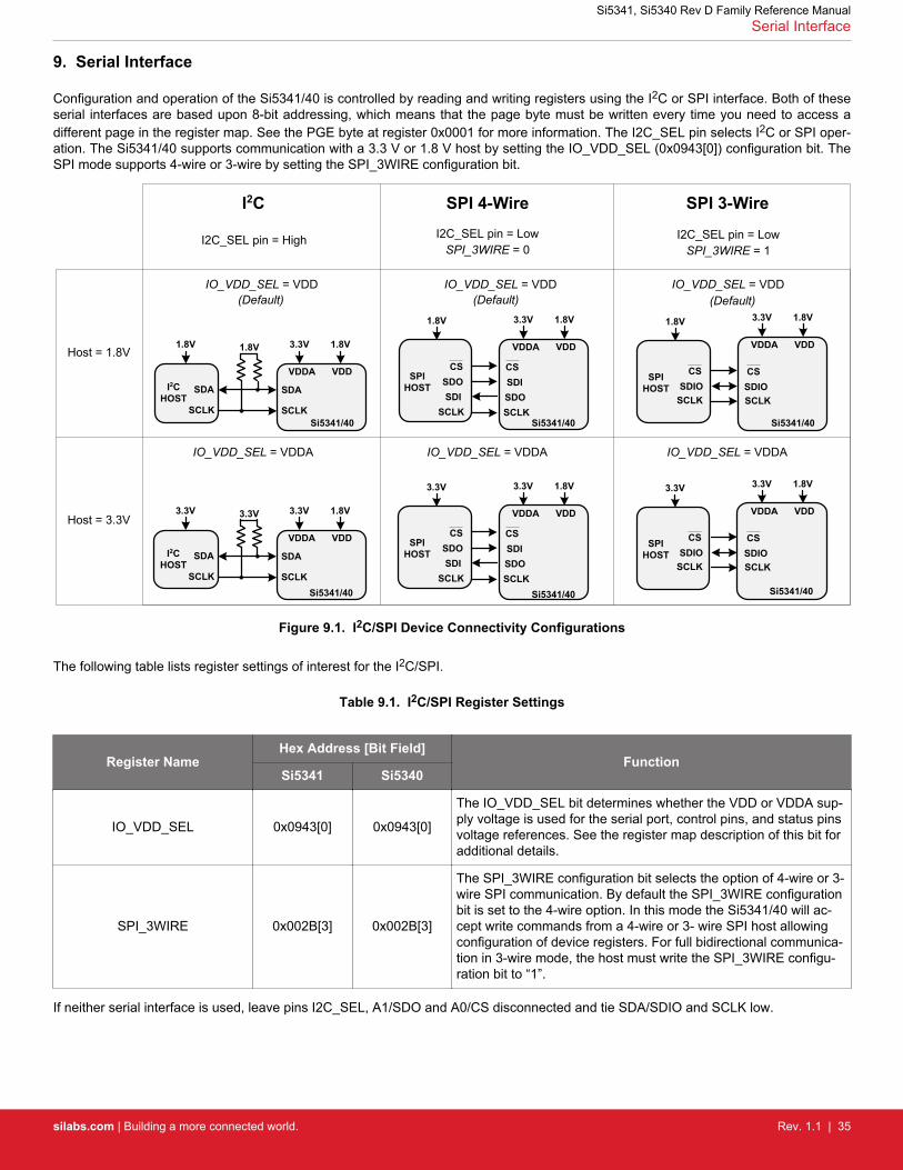
9. Serial Interface
Configuration and operation of the Si5341/40 is controlled by reading and writing registers using the I2C or SPI interface. Both of theseserial interfaces are based upon 8-bit addressing, which means that the page byte must be written every time you need to access adifferent page in the register map. See the PGE byte at register 0x0001 for more information. The I2C_SEL pin selects I2C or SPI oper-ation. The Si5341/40 supports communication with a 3.3 V or 1.8 V host by setting the IO_VDD_SEL (0x0943[0]) configuration bit. TheSPI mode supports 4-wire or 3-wire by setting the SPI_3WIRE configuration bit.
VDDA VDD
1.8V3.3V
Host = 3.3V
Host = 1.8V
I2C
I2C_SEL pin = High
IO_VDD_SEL = VDD IO_VDD_SEL = VDD
I2C_SEL pin = Low
SPI HOST
1.8V
SDISDOCSCS
SDOSDISCLKSCLK
Si5341/40
I2C HOST
1.8V
VDDA
SCLK
SDA
1.8V
VDD
1.8V3.3V
SPI HOST
1.8V
SDIOSDIOCSCS
SCLKSCLK
SPI_3WIRE = 0
SPI 4-Wire SPI 3-Wire
I2C_SEL pin = LowSPI_3WIRE = 1
IO_VDD_SEL = VDD
IO_VDD_SEL = VDDA IO_VDD_SEL = VDDA IO_VDD_SEL = VDDA
SCLK
SDA
(Default) (Default)
VDDA VDD
1.8V3.3V
(Default)
VDDA VDD
1.8V3.3V
SPI HOST
3.3V
SDISDOCSCS
SDOSDISCLKSCLK
I2C HOST
3.3V
VDDA
SCLK
SDA
3.3V
VDD
1.8V3.3V
SPI HOST
3.3V
SDIOSDIOCSCS
SCLKSCLKSCLK
SDA
VDDA VDD
1.8V3.3V
Si5341/40 Si5341/40
Si5341/40 Si5341/40 Si5341/40
Figure 9.1. I2C/SPI Device Connectivity Configurations
The following table lists register settings of interest for the I2C/SPI.
Table 9.1. I2C/SPI Register Settings
Register NameHex Address [Bit Field]
FunctionSi5341 Si5340
IO_VDD_SEL 0x0943[0] 0x0943[0]
The IO_VDD_SEL bit determines whether the VDD or VDDA sup-ply voltage is used for the serial port, control pins, and status pinsvoltage references. See the register map description of this bit foradditional details.
SPI_3WIRE 0x002B[3] 0x002B[3]
The SPI_3WIRE configuration bit selects the option of 4-wire or 3-wire SPI communication. By default the SPI_3WIRE configurationbit is set to the 4-wire option. In this mode the Si5341/40 will ac-cept write commands from a 4-wire or 3- wire SPI host allowingconfiguration of device registers. For full bidirectional communica-tion in 3-wire mode, the host must write the SPI_3WIRE configu-ration bit to “1”.
If neither serial interface is used, leave pins I2C_SEL, A1/SDO and A0/CS disconnected and tie SDA/SDIO and SCLK low.
Si5341, Si5340 Rev D Family Reference ManualSerial Interface
silabs.com | Building a more connected world. Rev. 1.1 | 35

9.1 I2C Interface
When in I2C mode, the serial interface operates in slave mode with 7-bit addressing and can operate in Standard-Mode (100 kbps) orFast-Mode (400 kbps) and supports burst data transfer with auto address increments. The I2C bus consists of a bidirectional serial dataline (SDA) and a serial clock input (SCL) as shown in Figure 9.12 SPI “Burst Data Write” Instruction Timing on page 41. Both the SDAand SCL pins must be connected to a supply via an external pull-up (1k to 4.7k ohm) as recommended by the I2C specification asshown in the figure below. Two address select bits (A0, A1) are provided allowing up to four Si5341/40 devices to communicate on thesame bus. This also allows four choices in the I2C address for systems that may have other overlapping addresses for other I2C devi-ces.
SDA
SCLK
Si5341/40
I2C_SEL
VDDVDDI2C
To I2C Bus or Host
A0A1
LSBs of I2C Address
I2C
Figure 9.2. I2C Configuration
The 7-bit slave device address of the Si5341/40 consists of a 5-bit fixed address plus two pins that are selectable for the last two bits,as shown in the following figure.
Slave Address 1 1 1 0 1 A0
0123456
A1
Figure 9.3. 7-bit I2C Slave Address Bit-Configuration
Data is transferred MSB first in 8-bit words as specified by the I2C specification. A write command consists of a 7-bit device (slave)address + a write bit, an 8-bit register address, and 8 bits of data as shown in Figure 9.6 SPI Interface Connections on page 38. Awrite burst operation is also shown where subsequent data words are written using to an auto-incremented address.
Si5341, Si5340 Rev D Family Reference ManualSerial Interface
silabs.com | Building a more connected world. Rev. 1.1 | 36

1 – Read0 – WriteA – Acknowledge (SDA LOW)N – Not Acknowledge (SDA HIGH)S – START conditionP – STOP condition
Write Operation – Single Byte
S 0 A Reg Addr [7:0]Slv Addr [6:0] A Data [7:0] PA
Write Operation - Burst (Auto Address Increment)
Reg Addr +1
S 0 A Reg Addr [7:0]Slv Addr [6:0] A Data [7:0] A Data [7:0] PA
Host
Si5341/40Host
Si5341/40
Figure 9.4. I2C Write Operation
A read operation is performed in two stages. A data write is used to set the register address, then a data read is performed to retrievethe data from the set address. A read burst operation is also supported as shown in the following figure.
1 – Read0 – WriteA – Acknowledge (SDA LOW)N – Not Acknowledge (SDA HIGH)S – START conditionP – STOP condition
Read Operation – Single Byte
S 0 A Reg Addr [7:0]Slv Addr [6:0] A P
Read Operation - Burst (Auto Address Increment)
Reg Addr +1
S 1 ASlv Addr [6:0] Data [7:0] PN
S 0 A Reg Addr [7:0]Slv Addr [6:0] A P
S 1 ASlv Addr [6:0] Data [7:0] A PNData [7:0]
Host
Si5341/40Host
Si5341/40
Figure 9.5. I2C Read Operation
Si5341, Si5340 Rev D Family Reference ManualSerial Interface
silabs.com | Building a more connected world. Rev. 1.1 | 37

9.2 SPI Interface
When in SPI mode, the serial interface operates in 4-wire or 3-wire depending on the state of the SPI_3WIRE configuration bit. The 4-wire interface consists of a clock input (SCLK), a chip select input (CS), serial data input (SDI), and serial data output (SDO). The 3-wire interface combines the SDI and SDO signals into a single bidirectional data pin (SDIO). Both 4-wire and 3-wire interface connec-tions are shown in the following figure.
To SPI HostSDI
SDO
Si5340/41
I2C_SEL
SCLK
CS
SPI_3WIRE = 0SPI 4-Wire
CS
SDIO
I2C_SEL
SCLK
SPI_3WIRE = 1SPI 3-Wire
To SPI HostTo SPI Host
Si5340/41
Figure 9.6. SPI Interface Connections
Table 9.2. SPI Command Format
Instruction Ist Byte11 2nd Byte 3rd Byte nth Byte2, 3
Set Address 000x xxxx 8-bit Address — —
Write Data 010x xxxx 8-bit Data — —
Read Data 100x xxxx 8-bit Data — —
Write Data + Address Increment 011x xxxx 8-bit Data — —
Read Data + Address Increment 101x xxxx 8-bit Data — —
Burst Write Data 1110 0000 8-bit Address 8-bit Data 8-bit Data
1. X = don’t care (1 or 0)2. The Burst Write Command is terminated by de-asserting CSb (CSb = high)3. There is no limit to the number of data bytes that may follow the Burst Write command, but the address will wrap around to 0 in
the byte after address 255 is written.
Writing or reading data consist of sending a “Set Address” command followed by a “Write Data” or “Read Data” command. The 'WriteData + Address Increment' or “Read Data + Address Increment” commands are available for cases where multiple byte operations insequential address locations is necessary. The “Burst Write Data” instruction provides a compact command format for writing datasince it uses a single instruction to define starting address and subsequent data bytes. The following figure shows an example of writingthree bytes of data using the write commands. This demonstrates that the “Write Burst Data” command is the most efficient method forwriting data to sequential address locations.
Si5341, Si5340 Rev D Family Reference ManualSerial Interface
silabs.com | Building a more connected world. Rev. 1.1 | 38
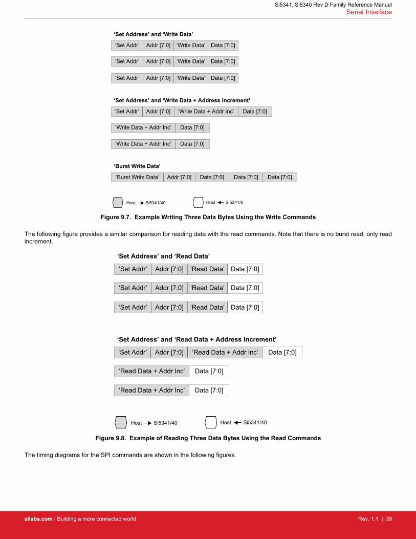
‘Set Address’ and ‘Write Data + Address Increment’
‘Burst Write Data’
‘Set Address’ and ‘Write Data’
‘Set Addr’ Addr [7:0] ‘Write Data’ Data [7:0]
‘Set Addr’ Addr [7:0] ‘Write Data’ Data [7:0]
‘Set Addr’ Addr [7:0] ‘Write Data’ Data [7:0]
‘Write Data + Addr Inc’ Data [7:0]
‘Write Data + Addr Inc’ Data [7:0]
‘Set Addr’ Addr [7:0] ‘Write Data + Addr Inc’ Data [7:0]
‘Burst Write Data’ Addr [7:0] Data [7:0] Data [7:0] Data [7:0]
Si5341/40Host Si5341/0Host
Figure 9.7. Example Writing Three Data Bytes Using the Write Commands
The following figure provides a similar comparison for reading data with the read commands. Note that there is no burst read, only readincrement.
‘Set Address’ and ‘Read Data + Address Increment’
‘Set Address’ and ‘Read Data’
‘Set Addr’ Addr [7:0] ‘Read Data’ Data [7:0]
‘Set Addr’ Addr [7:0] ‘Read Data’ Data [7:0]
‘Set Addr’ Addr [7:0] ‘Read Data’ Data [7:0]
‘Read Data + Addr Inc’ Data [7:0]
‘Read Data + Addr Inc’ Data [7:0]
‘Set Addr’ Addr [7:0] ‘Read Data + Addr Inc’ Data [7:0]
Si5341/40Host Si5341/40Host
Figure 9.8. Example of Reading Three Data Bytes Using the Read Commands
The timing diagrams for the SPI commands are shown in the following figures.
Si5341, Si5340 Rev D Family Reference ManualSerial Interface
silabs.com | Building a more connected world. Rev. 1.1 | 39
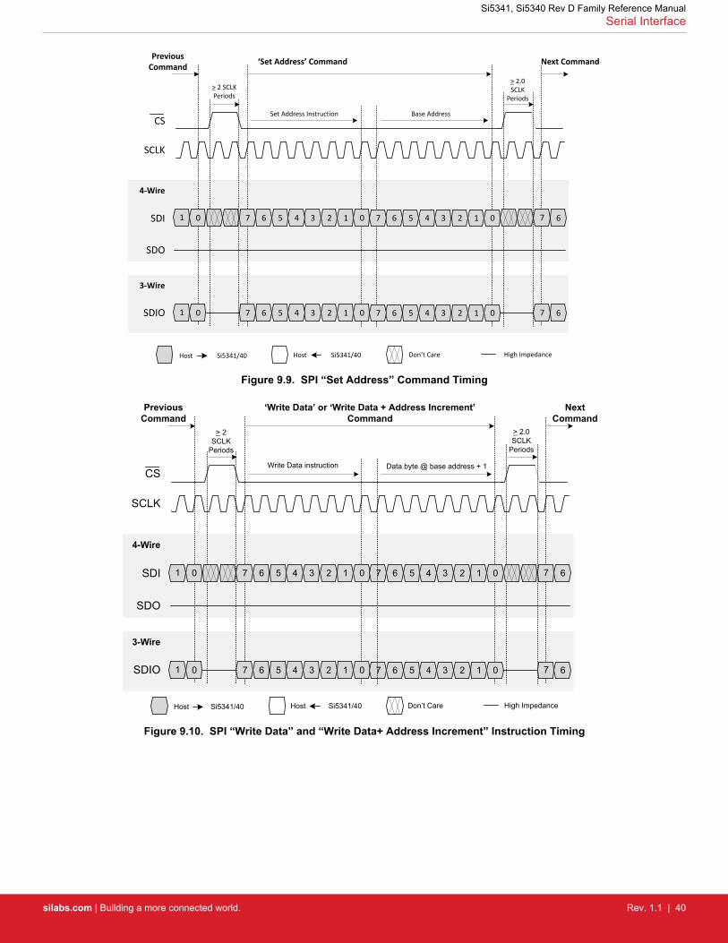
Set Address Instruction Base AddressCS
SCLK
SDI
SDO
SDIO
4-Wire
3-Wire
‘Set Address’ Command
> 2 SCLK Periods
Previous Command Next Command
> 2.0 SCLK
Periods
1 0 01234567 0123456 67
1 0 01234567 0123456 67
Si5341/40Host Si5341/40Host Don’t Care High Impedance
7
7
Figure 9.9. SPI “Set Address” Command Timing
Write Data instruction Data byte @ base address + 1CS
SCLK
SDI
SDO
SDIO
4-Wire
3-Wire
‘Write Data’ or ‘Write Data + Address Increment’ Command
> 2 SCLK
Periods
Previous Command
Next Command
1 0 01234567 01234567 67
1 0 01234567 01234567 67
Si5341/40Host Si5341/40Host Don’t Care High Impedance
> 2.0 SCLK
Periods
Figure 9.10. SPI “Write Data” and “Write Data+ Address Increment” Instruction Timing
Si5341, Si5340 Rev D Family Reference ManualSerial Interface
silabs.com | Building a more connected world. Rev. 1.1 | 40

CS
SCLK
SDI
SDO
SDIO
4-Wire
3-Wire
‘Read Data’ or ‘Read Data + Address Increment’ Command
Previous Command
Next Command
1 0 01234567
1 0 6701234567
1 0 01234567 67
67
01234567
Si5341/40Host Si5341/40Host Don’t Care High Impedance
Read Data instruction Read byte @ base address + 1
> 2.0 SCLK
Periods
> 2.0 SCLK
Periods
Figure 9.11. SPI “Read Data” and “Read Data + Address Increment” Instruction Timing
Burst Write Instruction Base addressCS
SCLK
SDO
SDIO
4-Wire
nth data byte @ base address +n
3-Wire
‘Burst Data Write’ CommandPrevious Command
SDI 1 0 01234567 0123456 0123456 01234567
1 0 01234567 0123456 0123456 0123456
Si5341/40Host Si5341/40Host Don’t Care High Impedance
1st data byte @ base address
6
Next Command
67
7 77
7 7 7
> 2.0 SCLK
Periods
> 2.0 SCLK
Periods
Figure 9.12. SPI “Burst Data Write” Instruction Timing
Si5341, Si5340 Rev D Family Reference ManualSerial Interface
silabs.com | Building a more connected world. Rev. 1.1 | 41

10. Field Programming
To simplify design and software development of systems using the Si5341/40, a field programmer is available. The ClockBuilder ProField Programmer supports both “in-system” programming (for devices already mounted on a PCB) as well as “in-socket” programmingof Si5341/40 sample devices. Refer to the ClockBuilder Pro Field Programmer product web page for information about this kit.
Si5341, Si5340 Rev D Family Reference ManualField Programming
silabs.com | Building a more connected world. Rev. 1.1 | 42

11. Recommended Crystals and External Oscillators
Please refer to the Si534x/8x Jitter Attenuators Recommended Crystal, TCXO and OCXOs Reference Manual for more information.
Si5341, Si5340 Rev D Family Reference ManualRecommended Crystals and External Oscillators
silabs.com | Building a more connected world. Rev. 1.1 | 43

12. Crystal and Device Circuit Layout Recommendations
The main layout issues that should be carefully considered include the following:• Number and size of the ground vias for the Epad (see Section 13.3 Grounding Vias for details)• Output clock trace routing• Input clock trace routing• Control and Status signals to input or output clock trace coupling• XTAL signal coupling• XTAL layout
If the application uses a crystal for the XAXB inputs a shield should be placed underneath the crystal connected to the X1 and X2 pins(4 and 7) to provide the best possible performance. The shield should not be connected to the ground plane and the planes underneathshould have as little under the shield as possible. It may be difficult to do this for all the layers, but it is important to do this for the layersthat are closest to the shield.
Refer to the High Performance Clock Generator Kits on the Clock Development Tools web page for the Si5341-EVB and Si5340-EVBschematics, layout, and BOM files.
12.1 64-Pin QFN Si5341 Layout Recommendations
This section details the recommended guidelines for the crystal layout of the 64-pin Si5341 device using an example 8-layer PCB. Fol-lowing are descriptions of each of the eight layers.• Layer 1: device layer, with low speed CMOS control/status signals, ground flooded• Layer 2: crystal shield• Layer 3: ground plane• Layer 4: power distribution• Layer 5: power routing layer• Layer 6: input clocks• Layer 7: output clocks layer• Layer 8: ground layer
Figure 12.1 64-pin Si5341 Crystal Layout Recommendations Top Layer (Layer 1) on page 45 is the top layer layout of the Si5341device mounted on the top PCB layer. This particular layout was designed to implement either a crystal or an external oscillator as theXAXB reference. The crystal/ oscillator area is outlined with the white box around it. In this case, the top layer is flooded with ground.Note that this layout has a resistor in series with each pin of the crystal. In typical applications, these resistors should be removed.
12.1.1 Si5341 Applications without a Crystal
If the application does not use a crystal, then the X1 and X2 pins should be left as “no connect” and should not be tied to ground. Inaddition, there is no need for a crystal shield or the voids underneath the shield. If there is a differential external clock input on XAXBthere should be a termination circuit near the XA and XB pins. This termination circuit should be two 50 Ω resistors and one 0.1 μF capconnected in the same manner as on the other clock inputs (IN0, IN1 and IN2). See Figure 5.1 Crystal Resonator and External Refer-ence Clock Connection Options on page 15. The clock input on XAXB must be ac-coupled. Care should be taken to keep all clockinputs well isolated from each other as well as any other dynamic signal. For LVCMOS or clipped sine wave inputs on XAXB, seeFigure 5.1 Crystal Resonator and External Reference Clock Connection Options on page 15.
Si5341, Si5340 Rev D Family Reference ManualCrystal and Device Circuit Layout Recommendations
silabs.com | Building a more connected world. Rev. 1.1 | 44
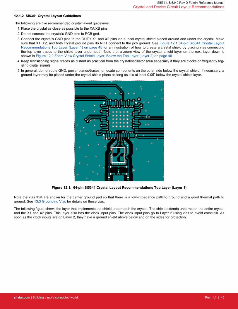
12.1.2 Si5341 Crystal Layout Guidelines
The following are five recommended crystal layout guidelines:1. Place the crystal as close as possible to the XA/XB pins.2. Do not connect the crystal's GND pins to PCB gnd.3. Connect the crystal's GND pins to the DUT's X1 and X2 pins via a local crystal shield placed around and under the crystal. Make
sure that X1, X2, and both crystal ground pins do NOT connect to the pcb ground. See Figure 12.1 64-pin Si5341 Crystal LayoutRecommendations Top Layer (Layer 1) on page 45 for an illustration of how to create a crystal shield by placing vias connectingthe top layer traces to the shield layer underneath. Note that a zoom view of the crystal shield layer on the next layer down isshown in Figure 12.2 Zoom View Crystal Shield Layer, Below the Top Layer (Layer 2) on page 46.
4. Keep transitioning signal traces as distant as practical from the crystal/oscillator area especially if they are clocks or frequently tog-gling digital signals.
5. In general, do not route GND, power planes/traces, or locate components on the other side below the crystal shield. If necessary, aground layer may be placed under the crystal shield plane as long as it is at least 0.05” below the crystal shield layer.
Figure 12.1. 64-pin Si5341 Crystal Layout Recommendations Top Layer (Layer 1)
Note the vias that are shown for the center ground pad so that there is a low-impedance path to ground and a good thermal path toground. See 13.3 Grounding Vias for details on these vias.
The following figure shows the layer that implements the shield underneath the crystal. The shield extends underneath the entire crystaland the X1 and X2 pins. This layer also has the clock input pins. The clock input pins go to Layer 2 using vias to avoid crosstalk. Assoon as the clock inputs are on Layer 2, they have a ground shield above below and on the sides for protection.
Si5341, Si5340 Rev D Family Reference ManualCrystal and Device Circuit Layout Recommendations
silabs.com | Building a more connected world. Rev. 1.1 | 45
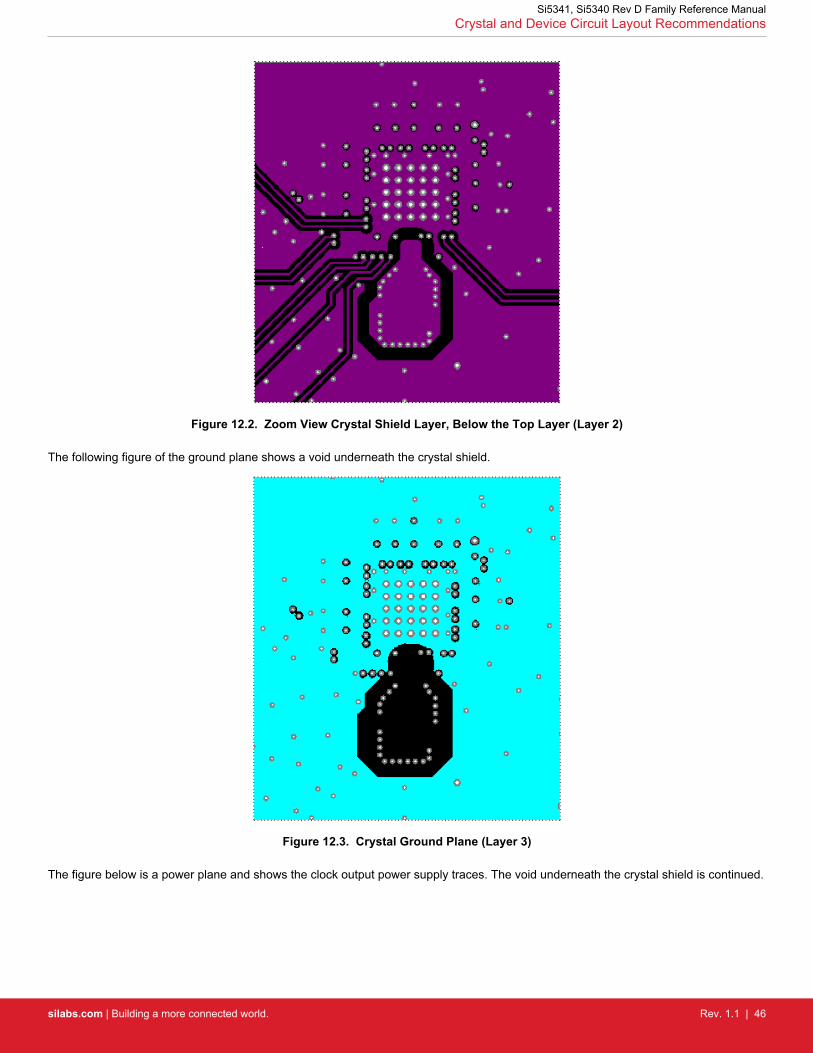
Figure 12.2. Zoom View Crystal Shield Layer, Below the Top Layer (Layer 2)
The following figure of the ground plane shows a void underneath the crystal shield.
Figure 12.3. Crystal Ground Plane (Layer 3)
The figure below is a power plane and shows the clock output power supply traces. The void underneath the crystal shield is continued.
Si5341, Si5340 Rev D Family Reference ManualCrystal and Device Circuit Layout Recommendations
silabs.com | Building a more connected world. Rev. 1.1 | 46

Figure 12.4. Power Plane (Layer 4)
The following figure shows Layer 5, which is the power plane with the power routed to the clock output power pins.
Figure 12.5. Layer 5 Power Routing on Power Plane (Layer 5)
The following figure is another ground plane similar to Layer 3.
Si5341, Si5340 Rev D Family Reference ManualCrystal and Device Circuit Layout Recommendations
silabs.com | Building a more connected world. Rev. 1.1 | 47

Figure 12.6. Ground Plane (Layer 6)
Si5341, Si5340 Rev D Family Reference ManualCrystal and Device Circuit Layout Recommendations
silabs.com | Building a more connected world. Rev. 1.1 | 48
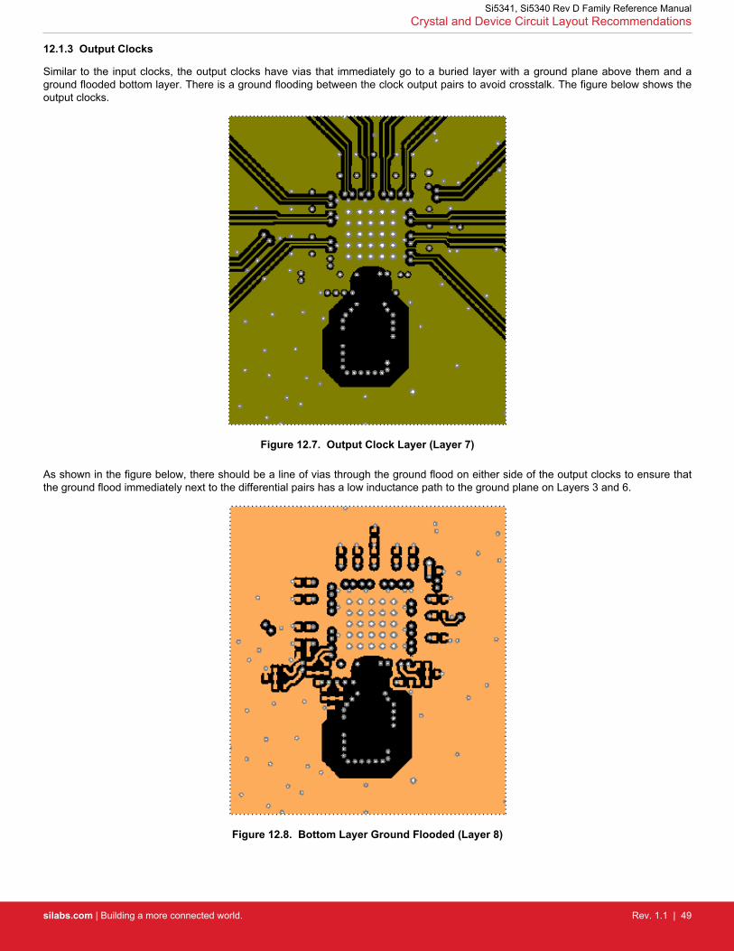
12.1.3 Output Clocks
Similar to the input clocks, the output clocks have vias that immediately go to a buried layer with a ground plane above them and aground flooded bottom layer. There is a ground flooding between the clock output pairs to avoid crosstalk. The figure below shows theoutput clocks.
Figure 12.7. Output Clock Layer (Layer 7)
As shown in the figure below, there should be a line of vias through the ground flood on either side of the output clocks to ensure thatthe ground flood immediately next to the differential pairs has a low inductance path to the ground plane on Layers 3 and 6.
Figure 12.8. Bottom Layer Ground Flooded (Layer 8)
Si5341, Si5340 Rev D Family Reference ManualCrystal and Device Circuit Layout Recommendations
silabs.com | Building a more connected world. Rev. 1.1 | 49
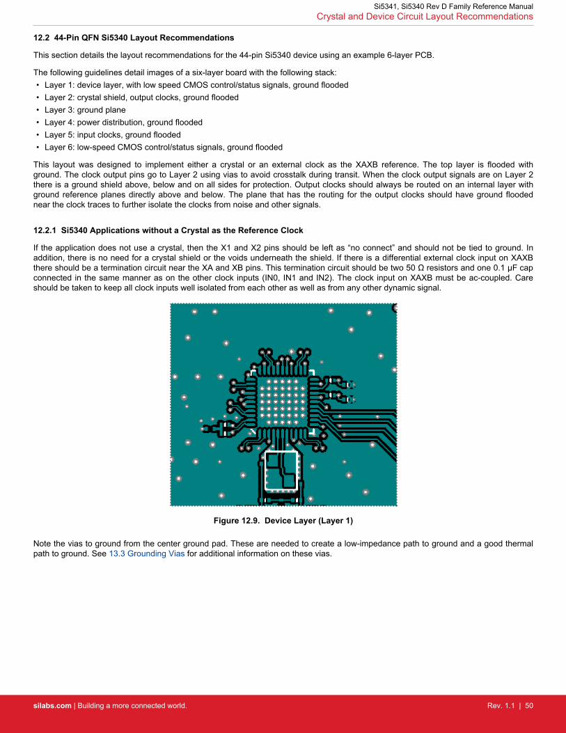
12.2 44-Pin QFN Si5340 Layout Recommendations
This section details the layout recommendations for the 44-pin Si5340 device using an example 6-layer PCB.
The following guidelines detail images of a six-layer board with the following stack:• Layer 1: device layer, with low speed CMOS control/status signals, ground flooded• Layer 2: crystal shield, output clocks, ground flooded• Layer 3: ground plane• Layer 4: power distribution, ground flooded• Layer 5: input clocks, ground flooded• Layer 6: low-speed CMOS control/status signals, ground flooded
This layout was designed to implement either a crystal or an external clock as the XAXB reference. The top layer is flooded withground. The clock output pins go to Layer 2 using vias to avoid crosstalk during transit. When the clock output signals are on Layer 2there is a ground shield above, below and on all sides for protection. Output clocks should always be routed on an internal layer withground reference planes directly above and below. The plane that has the routing for the output clocks should have ground floodednear the clock traces to further isolate the clocks from noise and other signals.
12.2.1 Si5340 Applications without a Crystal as the Reference Clock
If the application does not use a crystal, then the X1 and X2 pins should be left as “no connect” and should not be tied to ground. Inaddition, there is no need for a crystal shield or the voids underneath the shield. If there is a differential external clock input on XAXBthere should be a termination circuit near the XA and XB pins. This termination circuit should be two 50 Ω resistors and one 0.1 μF capconnected in the same manner as on the other clock inputs (IN0, IN1 and IN2). The clock input on XAXB must be ac-coupled. Careshould be taken to keep all clock inputs well isolated from each other as well as from any other dynamic signal.
Figure 12.9. Device Layer (Layer 1)
Note the vias to ground from the center ground pad. These are needed to create a low-impedance path to ground and a good thermalpath to ground. See 13.3 Grounding Vias for additional information on these vias.
Si5341, Si5340 Rev D Family Reference ManualCrystal and Device Circuit Layout Recommendations
silabs.com | Building a more connected world. Rev. 1.1 | 50

12.2.2 Si5340 Crystal Guidelines
The figure below is the second layer, which implements the shield underneath the crystal. The shield extends underneath the entirecrystal and the X1 and X2 pins. There should be no less than 12 vias to connect the X1X2 planes on Layers 1 and 2. These vias arenot shown in any other figures. All traces with signals that are not static must be kept well away from the crystal and the X1X2 plane.
Figure 12.10. Crystal Shield Layer 2
The following figure is the ground plane and shows a void underneath the crystal shield.
Figure 12.11. Ground Plane (Layer 3)
The following figure is a power plane showing the clock output power supply traces. The void underneath the crystal shield is continued.
Si5341, Si5340 Rev D Family Reference ManualCrystal and Device Circuit Layout Recommendations
silabs.com | Building a more connected world. Rev. 1.1 | 51
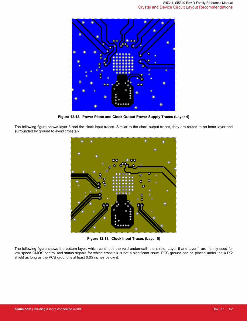
Figure 12.12. Power Plane and Clock Output Power Supply Traces (Layer 4)
The following figure shows layer 5 and the clock input traces. Similar to the clock output traces, they are routed to an inner layer andsurrounded by ground to avoid crosstalk.
Figure 12.13. Clock Input Traces (Layer 5)
The following figure shows the bottom layer, which continues the void underneath the shield. Layer 6 and layer 1 are mainly used forlow speed CMOS control and status signals for which crosstalk is not a significant issue. PCB ground can be placed under the X1X2shield as long as the PCB ground is at least 0.05 inches below it.
Si5341, Si5340 Rev D Family Reference ManualCrystal and Device Circuit Layout Recommendations
silabs.com | Building a more connected world. Rev. 1.1 | 52
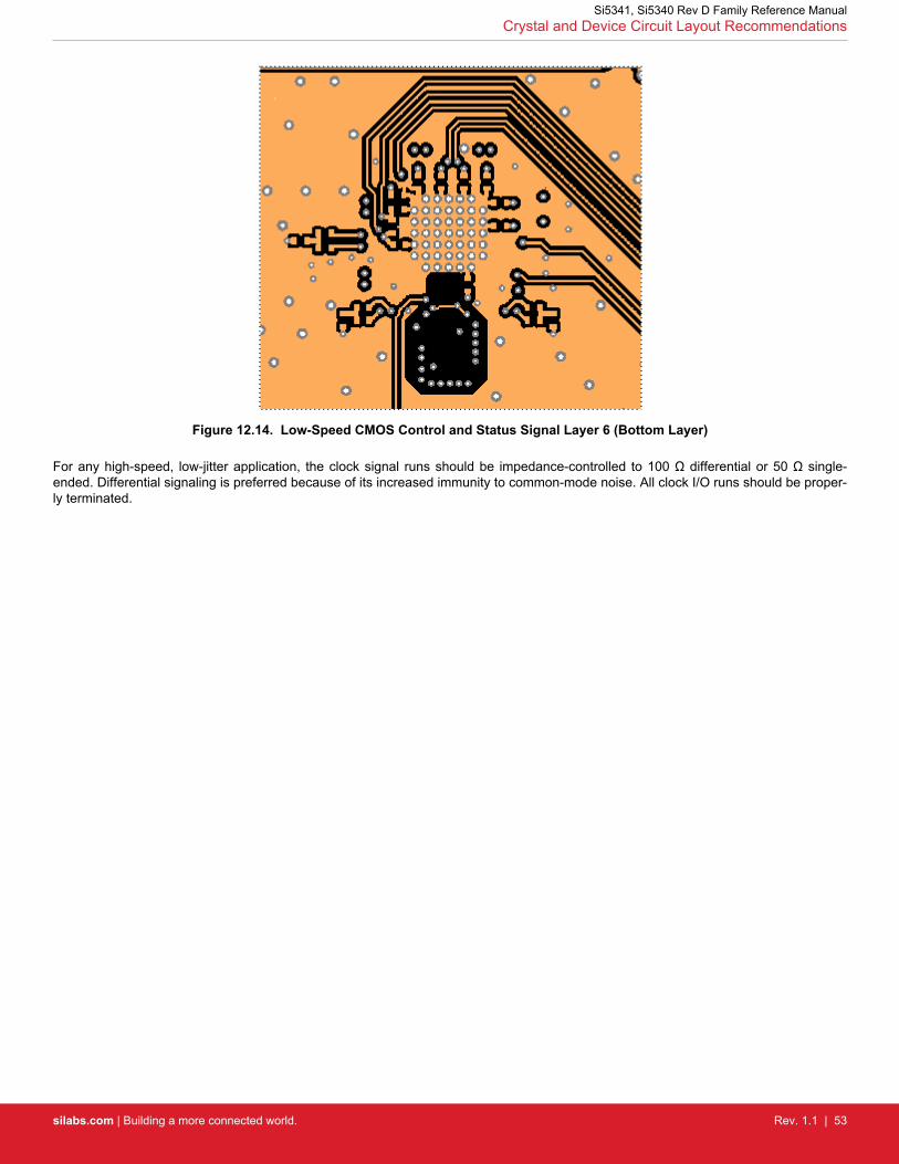
Figure 12.14. Low-Speed CMOS Control and Status Signal Layer 6 (Bottom Layer)
For any high-speed, low-jitter application, the clock signal runs should be impedance-controlled to 100 Ω differential or 50 Ω single-ended. Differential signaling is preferred because of its increased immunity to common-mode noise. All clock I/O runs should be proper-ly terminated.
Si5341, Si5340 Rev D Family Reference ManualCrystal and Device Circuit Layout Recommendations
silabs.com | Building a more connected world. Rev. 1.1 | 53

13. Power Management
13.1 Power Management Features
Several unused functions can be powered down to minimize power consumption. The registers listed in in the following table are usedfor powering down different features.
Table 13.1. Power Management Registers
Register NameHex Address [Bit Field] Function
Si5341 Si5340
PDN 0x001E[0] This bit allows powering down the device. The serial in-terface remains powered during power down mode.
OUT0_PDN
OUT1_PDN
OUT2_PDN
OUT3_PDN
OUT4_PDN
OUT5_PDN
OUT6_PDN
OUT7_PDN
OUT8_PDN
OUT9_PDN
0x0108[0]
0x010D[0]
0x0112[0]
0x0117[0]
0x011C[0]
0x0121[0]
0x0126[0]
0x012B[0]
0x0130[0]
0x013A[0]
0x0112[0]
0x011C[0]
0x0126[0]
0x012B[0]
—
—
—
—
—
—
Powers down unused clock outputs.
OUT_PDN_ALL 0x0145[0] Power down all output drivers
XAXB_PDNB 0x090E[1]0-Power down the oscillator and buffer circuitry at theXA/XB pins
1- No power down
13.2 Power Supply Recommendations
The power supply filtering generally is important for optimal timing performance. The Si5341/0 devices have multiple stages of on-chipregulation to minimize the impact of board level noise on clock jitter.
It is recommended to use a 0402, 1.0 μF ceramic capacitor on each VDD for optimal performance. Because of the extensive internalvoltage regulation this will be sufficient unless the power supply has very high noise. If the power supply might have very high noise,then it is suggested to include an optional, single 0603 (resistor/ferrite) bead in series with each supply to enable additional filtering.This resistor/ferrite should initially be a 0 Ω resistor. If additional supply filtering is needed then a ferrite component can replace the 0 Ωresistor.
13.3 Grounding Vias
The pad on the bottom of the device functions as both the sole electrical ground and primary heat transfer path. Hence it is important tominimize the inductance and maximize the heat transfer from this pad to the internal ground plane of the pcb. Use no less than 25 viasfrom the center pad to a ground plane under the device. In general more vias will perform better. Having the ground plane near the toplayer will also help to minimize the via inductance from the device to ground and maximize the heat transfer away from the device.
Si5341, Si5340 Rev D Family Reference ManualPower Management
silabs.com | Building a more connected world. Rev. 1.1 | 54

13.4 Power Supply Sequencing
Four classes of supply voltages exist:1. VDD = 1.8 V ± 5%2. VDDA = 3.3 V ± 5%3. VDDO = 1.8/2.5/3.3 V±5%4. VDDS = 1.8/3.3 V ±5%
There is no requirement for power supply sequencing unless the output clocks are required to be aligned. In this case the VDDO ofeach clock that needs to be aligned (low skew) must be powered up before VDD and VDDA. If this is not possible, then the output-output skew can be achieved by performing a SOFT_RST after the device is powered up.
On the Si5340, a VDDS pin exists but this pin only powers the driver for the status output pins LOLb and LOSXAXBB. There is nopower sequencing requirement for VDDS.
The internal POR (power on reset) will not happen until both VDD and VDDA have been applied.
Si5341, Si5340 Rev D Family Reference ManualPower Management
silabs.com | Building a more connected world. Rev. 1.1 | 55

14. Base vs. Factory Preprogrammed Devices
The Si5341/40 devices can be ordered as “base” or “factory-preprogrammed” (also known as “custom OPN”) versions.
14.1 “Base” Devices (Also Known as “Blank” Devices)
• Example “base” orderable part numbers (OPNs) are of the form “Si5341A-A-GM” or “Si5340B-A-GM”.• Base devices are available for applications where volatile reads and writes are used to program and configure the device for a par-
ticular application.• Base devices do not power up in a usable state (all output clocks are disabled).• Base devices are, however, configured by default to use a 48 MHz crystal on the XAXB reference and a 1.8V compatible I/O voltage
setting for the host I2C/SPI interface.• Additional programming of a base device is mandatory to achieve a usable configuration.• See the on-line lookup utility to access the default configuration plan and register settings for any base OPN.
14.2 Factory Preprogrammed (Custom OPN) Devices
• Factory preprogammed devices use a “custom OPN”, such as Si5341A-A-xxxxx-GM, where xxxxx is a sequence of characters as-signed by Silicon Labs for each customer-specific configuration. These characters are referred to as the “OPN ID”. Customers mustinitiate custom OPN creation using the ClockBuilder Pro software.
• Many customers prefer to order devices which are factory preprogrammed for a particular application that includes specifying theXAXB reference frequency/type, the clock input frequencies, the clock output frequencies, as well as the other options, such as au-tomatic clock selection, loop BW, etc. The ClockBuilder software is required to select among all of these options and to produce aproject file which Silicon Labs uses to preprogram all devices with custom orderable part number (“custom OPN”).
• Custom OPN devices contain all of the initiialization information in their non-volatile memory (NVM) so that it powers up fully config-ured and ready to go.
• Because preprogrammed device applications are inherently quite different from one another, the default power up values of the reg-ister settings can be determined using the custom OPN utility.
• Custom OPN devices include a device top mark which includes the unique OPN ID. Refer to the device datasheet’s Ordering Guideand Top Mark sections for more details.
Both “base” and “factory preprogrammed” devices can have their operating configurations changed at any time using volatile reads andwrites to the registers. Both types of devices can also have their current register configuration written to the NVM by executing an NVMbank burn sequence (see 3.2 NVM Programming).
Si5341, Si5340 Rev D Family Reference ManualBase vs. Factory Preprogrammed Devices
silabs.com | Building a more connected world. Rev. 1.1 | 56
15. Register Map
15.1 Register Map Overview and Default Settings Values
The Si5341/40 family has a large register map and is divided into separate pages. Each page contains a total of 256 registers, althoughall 256 registers are not used. Register 1 on each page is reserved to indicate the page and register 255 is reserved for the deviceready status. The following is a summary of the content that can be found on each of the pages. Note any page that is not listed is notused for the device. Do not attempt to write to registers that have not been described in this document, even if they are accessible.Note that the default value will depend on the values loaded into NVM, which is determined by the part number.
Where not provided in the register map information below, you can get the default values of the register map settings, by accessing thepart number lookup utility. Register map settings values are listed in the datasheet addendum, which can be accessed by using the linkabove. The register maps are broken out for the Si5341 and Si5340 separately.
15.2 Si5341 Register Map
Because preprogrammed devices are inherently quite different from one another, the default power up values of the registers can bedetermined using the custom OPN utility.
Table 15.1. Register Map Paging Descriptions
Page Start Address (Hex) Start Address (Decimal) Contents
Page 0 0000h 0 Alarms, interrupts, reset, device ID, revision ID
Page 1 0100h 256 Clock output configuration
Page 2 0200h 512 P,R dividers, scratch area
Page 3 0300h 768 Output N dividers, N divider FINC/FDEC
Page 9 0900h 2304 Control IO configuration
R = Read Only
R/W = Read Write
S = Self Clearing
Registers that are sticky are cleared by writing “0” to the bits that have been set in hardware. A self-clearing bit will clear on its ownwhen the state has changed.
Some registers that are listed in the Data Sheet Addendum are not documented in the Register Map below because they are set andmaintained by Clock Builder Pro. In almost all circumstances, these registers should not be modified by the user. For more details,please contact Silicon Labs.
Si5341, Si5340 Rev D Family Reference ManualRegister Map
silabs.com | Building a more connected world. Rev. 1.1 | 57

15.2.1 Page 0 Registers Si5341
Table 15.2. 0x0000 Die Rev
Reg Address Bit Field Type Setting Name Description
0x0000 3:0 R DIE_REV 4- bit Die Revision Number
0 = Silicon Revision A0
1 = Silicon Revision A1
Table 15.3. 0x0001 Page
Reg Address Bit Field Type Setting Name Description
0x0001 7:0 R/W PAGE Selects one of 256 possible pages.
There is the “Page Register” which is located at address 0x01 on every page. When read, it will indicate the current page. When writ-ten, it will change the page to the value entered. There is a page register at address 0x0001, 0x0101, 0x0201, 0x0301, … etc.
Table 15.4. 0x0002–0x0003 Base Part Number
Reg Address Bit Field Type Setting Name Description
0x0002 7:0 R PN_BASE Four-digit “base” part number, one nibble per digit
Example: Si5341A-A-GM. The base part number (OPN)is 5341, which is stored in this register
0x0003 15:8 R PN_BASE
Table 15.5. 0x0004 Device Speed/Synthesis Mode Grade
Reg Address Bit Field Type Setting Name Description
0x0004 7:0 R GRADE One ASCII character indicating the device speed grade:
0 = A
1 = B
2 = C
3 = D
Table 15.6. 0x0005 Device Revision
Reg Address Bit Field Type Setting Name Description
0x0005 7:0 R DEVICE_REV One ASCII character indicating the device revision lev-el:
0 = A; 1 = B
Example: in Si5341C-A12345-GM, the device revisionis “A” and is stored as 0.
Table 15.7. 0x0006–0x0008 Tool Version
Reg Address Bit Field Type Setting Name Description
0x0006 3:0 R TOOL_VERSION[3:0] Special
Si5341, Si5340 Rev D Family Reference ManualRegister Map
silabs.com | Building a more connected world. Rev. 1.1 | 58
Reg Address Bit Field Type Setting Name Description
0x0006 7:4 R TOOL_VERSION[7:4] Revision
0x0007 7:0 R TOOL_VERSION[15:8] Minor[7:0]
0x0008 0 R TOOL_VERSION[15:8] Minor[8]
0x0008 4:1 R TOOL_VERSION[16] Major
0x0008 7:5 R TOOL_VERSION[13:17] Tool. 0 for Clockbuilder Pro.
Table 15.8. 0x0009 Temperature Grade
Reg Address Bit Field Type Setting Name Description
0x0009 7:0 R TEMP_GRADE Device temperature grading
0 = Industrial (–40 ° C to 85 ° C) ambient conditions
Table 15.9. 0x000A Package ID
Reg Address Bit Field Type Setting Name Description
0x000A 7:0 R PKG_ID Package ID
0 = 9x9 mm 64 QFN
1 = 7x7 mm 44 QFN
Part numbers are of the form:
Si<Part Num Base><Grade>-<Device Revision><OPN ID>-<Temp Grade><Package ID>
Examples:
Si5341C-A12345-GM
Applies to a “custom” OPN (Ordering Part Number) device. These devices are factory pre-programmed with the frequency plan and allother operating characteristics defined by the user’s ClockBuilder Pro project file.
Si5341C-A-GM
Applies to a “base” or “blank” OPN device. Base devices are factory pre-programmed to a specific base part type (e.g., Si5341 butexclude any user-defined frequency plan or other user-defined operating characteristics selected in ClockBuilder Pro.
Table 15.10. 0x000B I2C Address
Reg Address Bit Field Type Setting Name Description
0x000B 6:2 R/W I2C_ADDR The upper 5 bits of the 7-bit I2C address.
The lower 2 bits are controlled by the A1 and A0 pins.
Table 15.11. 0x000C Status Bits
Reg Address Bit Field Type Setting Name Description
0x000C 0 R SYSINCAL 1 if the device is calibrating.
0x000C 1 R LOSXAXB 1 if there is no signal at the XA pin as the LOS detectoris only connected to the XA pin.
0x000C 2 R LOSREF 1 if the Phase Frequency detector does not have a sig-nal from XAXB, IN2, IN1, or IN0.
Si5341, Si5340 Rev D Family Reference ManualRegister Map
silabs.com | Building a more connected world. Rev. 1.1 | 59
Reg Address Bit Field Type Setting Name Description
0x000C 3 R LOL 1 if the DSPLL is out of lock.
0x000C 5 R SMBUS_TIMEOUT 1 if there is an SMBus timeout error.
Table 15.12. 0x000D INx Loss of Signal (LOS) Alarms
Reg Address Bit Field Type Setting Name Description
0x000D 3:0 R LOSIN 1 if no clock is present at [FB_IN, IN2, IN1, IN0]
Note that each bit corresponds to the input. The LOS bits are not sticky.• Input 0 (IN0) corresponds to LOS at 0x000D [0]• Input 1 (IN1) corresponds to LOS at 0x000D [1]• Input 2 (IN2) corresponds to LOS at 0x000D [2]• FB_IN corresponds to LOS at 0x000D[3]• See also LOSXAXB for LOS at the XAXB input
Table 15.13. 0x0011 Sticky Versions of Status Bits
Reg Address Bit Field Type Setting Name Description
0x0011 0 R SYSINCAL_FLG Sticky version of SYSINCAL. Write a 0 to clear theflag.
0x0011 1 R LOSXAXB_FLG Sticky version of LOSXAXB. Write a 0 to clear theflag.
0x0011 2 R LOSREF_FLG Sticky version of LOSREF. Write a 0 to clear theflag.
0x0011 3 R LOL_FLG Sticky version of LOL. Write a 0 to clear the flag.
0x0011 5 R SMBUS_TIMEOUT_FLG Sticky version of SMBUS_TIMEOUT. Write a 0 toclear the flag.
Table 15.14. 0x0012 INx LOS Flags
Reg Address Bit Field Type Setting Name Description
0x0012 3:0 R/W LOSIN_FLG Sticky version of LOS. Write a 0 to clear each individualflag.
Table 15.15. 0x0017 Status Flag Interrupt Masks
Reg Address Bit Field Type Setting Name Description
0x0017 0 R/W SYSINCAL_INTR_MSK 1 to mask SYSINCAL_FLG from causing an interrupt
0x0017 1 R/W LOSXAXB_INTR_MSK 1 to mask the LOSXAXB_FLG from causing an interrupt
0x0017 2 R/W LOSREF_INTR_MSK 1 to mask LOSREF_FLG from causing an interrupt
0x0017 3 R/W LOL_INTR_MSK 1 to mask LOL_FLG from causing an interrupt
0x0017 5 R/W SMB_TMOUT_INTR_MSK 1 to mask SMBUS_TIMEOUT_FLG from causing an in-terrupt
These are the interrupt mask bits for the fault flags in Register 0x0011. If a mask bit is set, the alarm will be blocked from causing aninterrupt.
Si5341, Si5340 Rev D Family Reference ManualRegister Map
silabs.com | Building a more connected world. Rev. 1.1 | 60
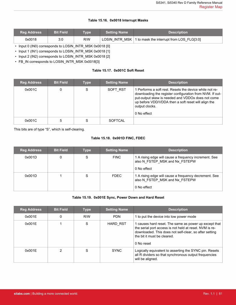
Table 15.16. 0x0018 Interrupt Masks
Reg Address Bit Field Type Setting Name Description
0x0018 3:0 R/W LOSIN_INTR_MSK 1 to mask the interrupt from LOS_FLG[3:0]
• Input 0 (IN0) corresponds to LOSIN_INTR_MSK 0x0018 [0]• Input 1 (IN1) corresponds to LOSIN_INTR_MSK 0x0018 [1]• Input 2 (IN2) corresponds to LOSIN_INTR_MSK 0x0018 [2]• FB_IN corresponds to LOSIN_INTR_MSK 0x0018[3]
Table 15.17. 0x001C Soft Reset
Reg Address Bit Field Type Setting Name Description
0x001C 0 S SOFT_RST 1 Performs a soft rest. Resets the device while not re-downloading the register configuration from NVM. If out-put-output skew is needed and VDDOx does not comeup before VDD/VDDA then a soft reset will align theoutput clocks.
0 No effect
0x001C 5 S SOFTCAL
This bits are of type “S”, which is self-clearing.
Table 15.18. 0x001D FINC, FDEC
Reg Address Bit Field Type Setting Name Description
0x001D 0 S FINC 1 A rising edge will cause a frequency increment. Seealso N_FSTEP_MSK and Nx_FSTEPW
0 No effect
0x001D 1 S FDEC 1 A rising edge will cause a frequency decrement. Seealso N_FSTEP_MSK and Nx_FSTEPW
0 No effect
Table 15.19. 0x001E Sync, Power Down and Hard Reset
Reg Address Bit Field Type Setting Name Description
0x001E 0 R/W PDN 1 to put the device into low power mode
0x001E 1 S HARD_RST 1 causes hard reset. The same as power up except thatthe serial port access is not held at reset. NVM is re-downloaded. This does not self-clear, so after settingthe bit it must be cleared.
0 No reset
0x001E 2 S SYNC Logically equivalent to asserting the SYNC pin. Resetsall R dividers so that synchronous output frequencieswill be aligned.
Si5341, Si5340 Rev D Family Reference ManualRegister Map
silabs.com | Building a more connected world. Rev. 1.1 | 61

Table 15.20. 0x0021 Input Clock Selection
Reg Address Bit Field Type Setting Name Description
0x0021 0 R/W IN_SEL_REGCTRL Selects between register controlled reference clock se-lection and pin controlled clock selection using IN_SEL1and IN_SEL0 pins: 0 for pin controlled clock selection; 1for register clock selection via IN_SEL bits.
0x0021 2:1 R/W IN_SEL Selects the reference clock input to the PLL whenIN_SEL_REGCTRL=1.
0 IN0
1 IN1
2 IN2
3 XA/XB
Table 15.21. 0x002B SPI 3 vs. 4 Wire
Reg Address Bit Field Type Setting Name Description
0x002B 3 R/W SPI_3WIRE 0 for 4-wire SPI, 1 for 3-wire SPI
Table 15.22. 0x002C LOS Enable
Reg Address Bit Field Type Setting Name Description
0x002C 3:0 R/W LOS_EN 1 to enable LOS for the inputs other than XAXB;
0 for disable
0x002C 4 R/W LOSXAXB_DIS 1 to disable LOS for the XAXB input
• Input 0 (IN0): LOS_EN[0]• Input 1 (IN1): LOS_EN[1]• Input 2 (IN2): LOS_EN[2]• FB_IN: LOS_EN[3]
Table 15.23. 0x002D Loss of Signal Requalification Time
Reg Address Bit Field Type Setting Name Description
0x002D 1:0 R/W LOS0_VAL_TIME Clock Input 0
0 for 2 msec
1 for 100 msec
2 for 200 msec
3 for one second
0x002D 3:2 R/W LOS1_VAL_TIME Clock Input 1, same as above
0x002D 5:4 R/W LOS2_VAL_TIME Clock Input 2, same as above
0x002D 7:6 R/W LOS3_VAL_TIME Clock Input 3, same as above
When an input clock is gone (and therefore has an active LOS alarm), if the clock returns, there is a period of time that the clock mustbe within the acceptable range before the alarm is removed. This is the LOS_VAL_TIME.
Si5341, Si5340 Rev D Family Reference ManualRegister Map
silabs.com | Building a more connected world. Rev. 1.1 | 62
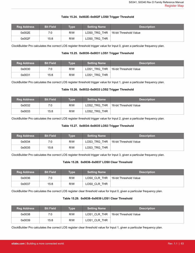
Table 15.24. 0x002E–0x002F LOS0 Trigger Threshold
Reg Address Bit Field Type Setting Name Description
0x002E 7:0 R/W LOS0_TRG_THR 16-bit Threshold Value
0x002F 15:8 R/W LOS0_TRG_THR
ClockBuilder Pro calculates the correct LOS register threshold trigger value for Input 0, given a particular frequency plan.
Table 15.25. 0x0030–0x0031 LOS1 Trigger Threshold
Reg Address Bit Field Type Setting Name Description
0x0030 7:0 R/W LOS1_TRG_THR 16-bit Threshold Value
0x0031 15:8 R/W LOS1_TRG_THR
ClockBuilder Pro calculates the correct LOS register threshold trigger value for Input 1, given a particular frequency plan.
Table 15.26. 0x0032–0x0033 LOS2 Trigger Threshold
Reg Address Bit Field Type Setting Name Description
0x0032 7:0 R/W LOS2_TRG_THR 16-bit Threshold Value
0x0033 15:8 R/W LOS2_TRG_THR
ClockBuilder Pro calculates the correct LOS register threshold trigger value for Input 2, given a particular frequency plan.
Table 15.27. 0x0034–0x0035 LOS3 Trigger Threshold
Reg Address Bit Field Type Setting Name Description
0x0034 7:0 R/W LOS3_TRG_THR 16-bit Threshold Value
0x0035 15:8 R/W LOS3_TRG_THR
ClockBuilder Pro calculates the correct LOS register threshold trigger value for Input 3, given a particular frequency plan.
Table 15.28. 0x0036–0x0037 LOS0 Clear Threshold
Reg Address Bit Field Type Setting Name Description
0x0036 7:0 R/W LOS0_CLR_THR 16-bit Threshold Value
0x0037 15:8 R/W LOS0_CLR_THR
ClockBuilder Pro calculates the correct LOS register clear threshold value for Input 0, given a particular frequency plan.
Table 15.29. 0x0038–0x0039 LOS1 Clear Threshold
Reg Address Bit Field Type Setting Name Description
0x0038 7:0 R/W LOS1_CLR_THR 16-bit Threshold Value
0x0039 15:8 R/W LOS1_CLR_THR
ClockBuilder Pro calculates the correct LOS register clear threshold value for Input 1, given a particular frequency plan.
Si5341, Si5340 Rev D Family Reference ManualRegister Map
silabs.com | Building a more connected world. Rev. 1.1 | 63

Table 15.30. 0x003A–0x003B LOS2 Clear Threshold
Reg Address Bit Field Type Setting Name Description
0x003A 7:0 R/W LOS2_CLR_THR 16-bit Threshold Value
0x003B 15:8 R/W LOS2_CLR_THR
ClockBuilder Pro calculates the correct LOS register clear threshold value for Input 2, given a particular frequency plan.
Table 15.31. 0x003C–0x003D LOS3 Clear Threshold
Reg Address Bit Field Type Setting Name Description
0x003C 7:0 R/W LOS3_CLR_THR 16-bit Threshold Value
0x003D 15:8 R/W LOS3_CLR_THR
ClockBuilder Pro calculates the correct LOS register clear threshold value for Input 3, given a particular frequency plan.
Table 15.32. 0x0041–0x0044 LOS Pre-Divider for IN0, IN1, IN3, FB_IN
Reg Address Bit Field Type Setting Name Description
0x0041 7:0 R/W LOS0_DIV_SEL A pre-divider that is configured by ClockBuilder Pro
0x0042 7:0 R/W LOS1_DIV_SEL A pre-divider that is configured by ClockBuilder Pro
0x0043 7:0 R/W LOS2_DIV_SEL A pre-divider that is configured by ClockBuilder Pro
0x0044 7:0 R/W LOS3_DIV_SEL A pre-divider that is configured by ClockBuilder Pro
The following are the pre-divider values for the above-listed registers values.
Si5341, Si5340 Rev D Family Reference ManualRegister Map
silabs.com | Building a more connected world. Rev. 1.1 | 64

Register Value (Decimal) Divider Value
0 1 (bypass)
1 2
2 4
3 8
4 16
5 32
6 64
7 128
8 256
9 512
10 1024
11 2048
12 4096
13 8192
14 16384
15 32768
16 65536
Table 15.33. 0x009E
Reg Address Bit Field Type Setting Name Description
0x0038 7:4 R/W LOL_SET_THR
Table 15.34. 0x00E2 Active NVM Bank
Reg Address Bit Field Type Setting Name Description
0x00E2 7:0 R AC-TIVE_NVM_BANK
0x033 when no NVM burn by customer
0x0F when 1 NVM bank has been burned by customer
0x3F when 2 NVM banks have been burned by custom-er
When ACTIVE_NVM_BANK = 0x3F, the last bank hasalready been burned. See 3.2 NVM Programming for adetailed description of how to program the NVM.
Table 15.35. 0x00E3
Reg Address Bit Field Type Setting Name Description
0x00E3 7:0 R/W NVM_WRITE Write 0xC7 to initiate an NVM bank burn.
Si5341, Si5340 Rev D Family Reference ManualRegister Map
silabs.com | Building a more connected world. Rev. 1.1 | 65

Table 15.36. 0x00E4
Reg Address Bit Field Type Setting Name Description
0x00E4 0 S NVM_READ_BANK When set, this bit will read the NVM down into the vola-tile memory.
Table 15.37. 0x00F6
Reg Address Bit Field Type Setting Name Description
0x00F6 0 R/W REG_0XF7_INTR
0x00F6 1 R/W REG_0XF8_INTR
0x00F6 2 R/W REG_0XF9_INTR
Table 15.38. 0x00F7
Reg Address Bit Field Type Setting Name Description
0x00F7 0 R/W SYSINCAL_INTR
0x00F7 1 R/W LOSXAXB_INTR
0x00F7 2 R/W LOSREF_INTR
0x00F7 3 R/W LOL_INTR
0x00F7 4 R/W LOSVCO_INTR
0x00F7 5 R/W SMBUS_TIME_OUT_
INTR
Table 15.39. 0x00F8
Reg Address Bit Field Type Setting Name Description
0x00F8 3:0 R/W LOS_INTR
Table 15.40. 0x00F9
Reg Address Bit Field Type Setting Name Description
0x00F9 0 R/W LOL_INTR_PLLA
0x00F9 1 R/W LOL_INTR_PLLB
0x00F9 2 R/W LOL_INTR_PLLC
0x00F9 3 R/W LOL_INTR_PLLD
0x00F9 4 R/W HOLD_INTR_PLLA
0x00F9 5 R/W HOLD_INTR_PLLB
0x00F9 6 R/W HOLD_INTR_PLLC
0x00F9 7 R/W HOLD_INTR_PLLD
Si5341, Si5340 Rev D Family Reference ManualRegister Map
silabs.com | Building a more connected world. Rev. 1.1 | 66

15.2.2 Page 1 Registers Si5341
Table 15.41. 0x0102 All Output Clock Driver Disable
Reg Address Bit Field Type Setting Name Description
0x0102 0 R/W OUTALL_DISA-BLE_LOW
0: Disables all output drivers.
1: No output drivers are disabled by this bit, but othersignals may disable the outputs.
Table 15.42. 0x0108 Clock Output 0 Configs and DIV2 Mode
Reg Address Bit Field Type Setting Name Description
0x0108 0 R/W OUT0_PDN Output driver 0: 0 to power up the driver, 1 to powerdown the driver. Clock outputs will be weakly pulled-low.
0x0108 1 R/W OUT0_OE Output driver 0: 0 to disable the output, 1 to enable theoutput
0x0108 2 R/W OUT0_RDIV_FORCE2
0 R0 divider value is set by R0_REG
1 R0 divider value is forced into divide by 2
Table 15.43. 0x0109 Clock Output 0 Format
Reg Address Bit Field Type Setting Name Description
0x0109 2:0 R/W OUT0_FORMAT 0: Reserved
1: normal differential
2: low power differential
3: reserved
4: LVCMOS
5–7: Reserved
0x0109 3 R/W OUT0_SYNC_EN 0 disable
1: Enable
Enable/disable synchronized (glitchless) operation.When enabled, the power down and output enables aresynchronized to the output clock.
0x0109 5:4 R/W OUT0_DIS_STATE Determines the state of an output driver when disabled,selectable as:
0: Disable in low state
1: Disable in high state
2: Reserved
3: Reserved
0x0109 7:6 R/W OUT0_CMOS_DRV LVCMOS output impedance. See Table 6.4 Settings forLVDS, LVPECL, and HCSL on page 24.
See 6.2 Performance Guidelines for Outputs.
Si5341, Si5340 Rev D Family Reference ManualRegister Map
silabs.com | Building a more connected world. Rev. 1.1 | 67
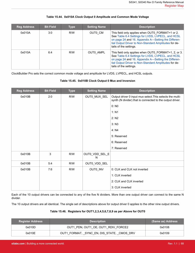
Table 15.44. 0x010A Clock Output 0 Amplitude and Common Mode Voltage
Reg Address Bit Field Type Setting Name Description
0x010A 3:0 R/W OUT0_CM This field only applies when OUT0_FORMAT=1 or 2.See Table 6.4 Settings for LVDS, LVPECL, and HCSLon page 24 and 16. Appendix A—Setting the Differen-tial Output Driver to Non-Standard Amplitudes for de-tails of the settings.
0x010A 6:4 R/W OUT0_AMPL This field only applies when OUT0_FORMAT=1, 2, or 3.See Table 6.4 Settings for LVDS, LVPECL, and HCSLon page 24 and 16. Appendix A—Setting the Differen-tial Output Driver to Non-Standard Amplitudes for de-tails of the settings.
ClockBuilder Pro sets the correct common mode voltage and amplitude for LVDS, LVPECL, and HCSL outputs.
Table 15.45. 0x010B Clock Output 0 Mux and Inversion
Reg Address Bit Field Type Setting Name Description
0x010B 2:0 R/W OUT0_MUX_SEL Output driver 0 input mux select.This selects the multi-synth (N divider) that is connected to the output driver.
0: N0
1: N1
2: N2
3: N3
4: N4
5: Reserved
6: Reserved
7: Reserved
0x010B 3 R/W OUT0_VDD_SEL_EN
0x010B 5:4 R/W OUT0_VDD_SEL
0x010B 7:6 R/W OUT0_INV 0: CLK and CLK not inverted
1: CLK inverted
2: CLK and CLK inverted
3: CLK inverted
Each of the 10 output drivers can be connected to any of the five N dividers. More than one output driver can connect to the same Ndivider.
The 10 output drivers are all identical. The single set of descriptions above for output driver 0 applies to the other nine output drivers.
Table 15.46. Registers for OUT1,2,3,4,5,6,7,8,9 as per Above for OUT0
Register Address Description (Same as) Address
0x010D OUT1_PDN, OUT1_OE, OUT1_RDIV_FORCE2 0x0108
0x010E OUT1_FORMAT, _SYNC_EN, DIS_STATE, _CMOS_DRV 0x0109
Si5341, Si5340 Rev D Family Reference ManualRegister Map
silabs.com | Building a more connected world. Rev. 1.1 | 68
Register Address Description (Same as) Address
0x010F OUT1_CM, OUT1_AMPL 0x010A
0x0110 OUT1_MUX_SEL, OUT1_VDD_SEL_EN, OUT1_VDD_SEL, OUT1_INV 0x010B
0x0112 OUT2_PDN, OUT2_OE, OUT2_RDIV_FORCE2 0x0108
0x0113 OUT2_FORMAT, _SYNC_EN, DIS_STATE, _CMOS_DRV 0x0109
0x0114 OUT2_CM, OUT2_AMPL 0x010A
0x0115 OUT2_MUX_SEL, OUT2_VDD_SEL_EN, OUT2_VDD_SEL, OUT2_INV 0x010B
0x0117 OUT3_PDN, OUT3_OE, OUT3_RDIV_FORCE2 0x0108
0x0118 OUT3_FORMAT, _SYNC_EN, DIS_STATE, _CMOS_DRV 0x0109
0x0119 OUT3_CM, OUT3_AMPL 0x010A
0x011A OUT3_MUX_SEL, OUT3_VDD_SEL_EN, OUT3_VDD_SEL, OUT3_INV 0x010B
0x011C OUT4_PDN, OUT4_OE, OUT4_RDIV_FORCE2 0x0108
0x011D OUT4_FORMAT, _SYNC_EN, DIS_STATE, _CMOS_DRV 0x010A
0x011E OUT4_CM, OUT4_AMPL 0x0105
0x011F OUT4_MUX_SEL, OUT4_VDD_SEL_EN, OUT4_VDD_SEL, OUT4_INV 0x010B
0x0121 OUT5_PDN, OUT5_OE, OUT5_RDIV_FORCE2 0x0108
0x0122 OUT5_FORMAT, _SYNC_EN, DIS_STATE, _CMOS_DRV 0x0109
0x0123 OUT5_CM, OUT5_AMPL 0x010A
0x0124 OUT5_MUX_SEL, OUT5_VDD_SEL_EN, OUT5_VDD_SEL, OUT5_INV 0x010B
0x0126 OUT6_PDN, OUT6_OE, OUT6_RDIV_FORCE2 0x0108
0x0127 OUT6_FORMAT, _SYNC_EN, DIS_STATE, _CMOS_DRV 0x010A
0x0128 OUT6_CM, OUT6_AMPL 0x0109
0x0129 OUT6_MUX_SEL, OUT6_VDD_SEL_EN, OUT6_VDD_SEL, OUT6_INV 0x010B
0x012B OUT7_PDN, OUT7_OE, OUT7_RDIV_FORCE2 0x0108
0x012C OUT7_FORMAT, _SYNC_EN, DIS_STATE, _CMOS_DRV 0x0109
0x012D OUT7_CM, OUT7_AMPL 0x010A
0x012E OUT7_MUX_SEL, OUT7_VDD_SEL_EN, OUT7_VDD_SEL, OUT7_INV 0x010B
0x0130 OUT8_PDN, OUT8_OE, OUT8_RDIV_FORCE2 0x0108
0x0131 OUT8_FORMAT, _SYNC_EN, DIS_STATE, _CMOS_DRV 0x0109
0x0132 OUT8_CM, OUT8_AMPL 0x010A
0x0133 OUT8_MUX_SEL, OUT8_VDD_SEL_EN, OUT8_VDD_SEL, OUT8_INV 0x010B
0x013A OUT9_PDN, OUT9_OE, OUT9_RDIV_FORCE2 0x0108
0x013B OUT9_FORMAT, _SYNC_EN, DIS_STATE, _CMOS_DRV 0x0109
0x013C OUT9_CM, OUT9_AMPL 0x010A
0x013D OUT9_MUX_SEL, OUT9_VDD_SEL_EN, OUT9_VDD_SEL, OUT9_INV 0x010B
Si5341, Si5340 Rev D Family Reference ManualRegister Map
silabs.com | Building a more connected world. Rev. 1.1 | 69
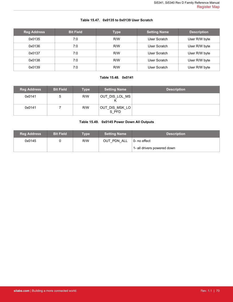
Table 15.47. 0x0135 to 0x0139 User Scratch
Reg Address Bit Field Type Setting Name Description
0x0135 7:0 R/W User Scratch User R/W byte
0x0136 7:0 R/W User Scratch User R/W byte
0x0137 7:0 R/W User Scratch User R/W byte
0x0138 7:0 R/W User Scratch User R/W byte
0x0139 7:0 R/W User Scratch User R/W byte
Table 15.48. 0x0141
Reg Address Bit Field Type Setting Name Description
0x0141 5 R/W OUT_DIS_LOL_MSK
0x0141 7 R/W OUT_DIS_MSK_LOS_PFD
Table 15.49. 0x0145 Power Down All Outputs
Reg Address Bit Field Type Setting Name Description
0x0145 0 R/W OUT_PDN_ALL 0- no effect
1- all drivers powered down
Si5341, Si5340 Rev D Family Reference ManualRegister Map
silabs.com | Building a more connected world. Rev. 1.1 | 70
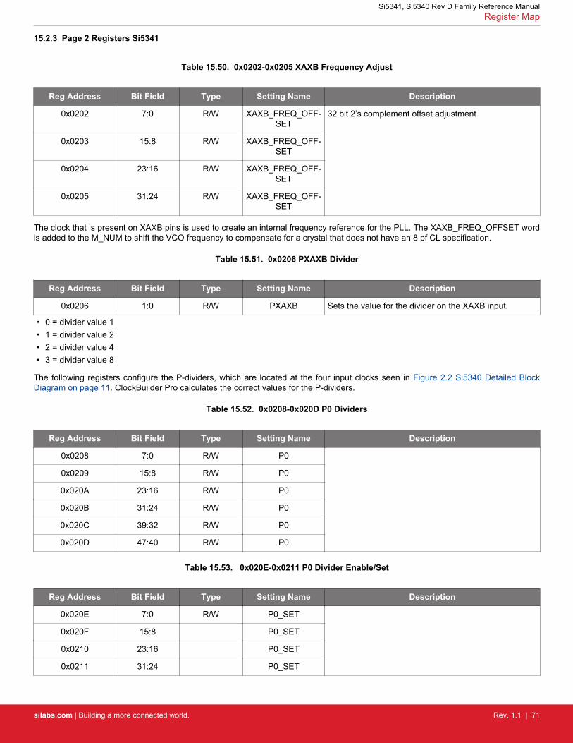
15.2.3 Page 2 Registers Si5341
Table 15.50. 0x0202-0x0205 XAXB Frequency Adjust
Reg Address Bit Field Type Setting Name Description
0x0202 7:0 R/W XAXB_FREQ_OFF-SET
32 bit 2’s complement offset adjustment
0x0203 15:8 R/W XAXB_FREQ_OFF-SET
0x0204 23:16 R/W XAXB_FREQ_OFF-SET
0x0205 31:24 R/W XAXB_FREQ_OFF-SET
The clock that is present on XAXB pins is used to create an internal frequency reference for the PLL. The XAXB_FREQ_OFFSET wordis added to the M_NUM to shift the VCO frequency to compensate for a crystal that does not have an 8 pf CL specification.
Table 15.51. 0x0206 PXAXB Divider
Reg Address Bit Field Type Setting Name Description
0x0206 1:0 R/W PXAXB Sets the value for the divider on the XAXB input.
• 0 = divider value 1• 1 = divider value 2• 2 = divider value 4• 3 = divider value 8
The following registers configure the P-dividers, which are located at the four input clocks seen in Figure 2.2 Si5340 Detailed BlockDiagram on page 11. ClockBuilder Pro calculates the correct values for the P-dividers.
Table 15.52. 0x0208-0x020D P0 Dividers
Reg Address Bit Field Type Setting Name Description
0x0208 7:0 R/W P0
0x0209 15:8 R/W P0
0x020A 23:16 R/W P0
0x020B 31:24 R/W P0
0x020C 39:32 R/W P0
0x020D 47:40 R/W P0
Table 15.53. 0x020E-0x0211 P0 Divider Enable/Set
Reg Address Bit Field Type Setting Name Description
0x020E 7:0 R/W P0_SET
0x020F 15:8 P0_SET
0x0210 23:16 P0_SET
0x0211 31:24 P0_SET
Si5341, Si5340 Rev D Family Reference ManualRegister Map
silabs.com | Building a more connected world. Rev. 1.1 | 71

Table 15.54. 0x0212-0x0217 P1 Dividers
Reg Address Bit Field Type Setting Name Description
0x0212 7:0 R/W P1
0x0213 15:8 R/W P1
0x0214 23:16 R/W P1
0x0215 31:24 R/W P1
0x0216 39:32 R/W P1
0x0217 47:40 R/W P1
Table 15.55. 0x0218-0x021B P1 Divider Enable/Set
Reg Address Bit Field Type Setting Name Description
0x0218 7:0 R/W P1_SET
0x0219 15:8 P1_SET
0x021A 23:16 P1_SET
0x021B 31:24 P1_SET
Table 15.56. 0x021C-0x0221 P2 Dividers
Reg Address Bit Field Type Setting Name Description
0x021C 7:0 R/W P2
0x021D 15:8 R/W P2
0x021E 23:16 R/W P2
0x021F 31:24 R/W P2
0x0220 39:32 R/W P2
0x0221 47:40 R/W P2
Table 15.57. 0x0222-0x0225 P2 Divider Enable/Set
Reg Address Bit Field Type Setting Name Description
0x0222 7:0 R/W P2_SET
0x0223 15:8 P2_SET
0x0224 23:16 P2_SET
0x0225 31:24 P2_SET
Table 15.58. 0x0226-0x022B P3 Dividers
Reg Address Bit Field Type Setting Name Description
0x0226 7:0 R/W P3
0x0227 15:8 R/W P3
Si5341, Si5340 Rev D Family Reference ManualRegister Map
silabs.com | Building a more connected world. Rev. 1.1 | 72

Reg Address Bit Field Type Setting Name Description
0x0228 23:16 R/W P3
0x0229 31:24 R/W P3
0x022A 39:32 R/W P3
0x022B 47:40 R/W P3
Table 15.59. 0x022C-0x022F P3 Divider Enable/Set
Reg Address Bit Field Type Setting Name Description
0x022C 7:0 R/W P3_SET
0x022D 15:8 P3_SET
0x022E 23:16 P3_SET
0x022F 31:24 P3_SET
Table 15.60. 0x0230 P Divider Update Bits
Reg Address Bit Field Type Setting Name Description
0x0230 0 S P0_UPDATE Must write a 1 to this bit to cause a change to the P0divider to take effect.
0x0230 1 S P1_UPDATE Must write a 1 to this bit to cause a change to the P1divider to take effect.
0x0230 2 S P2_UPDATE Must write a 1 to this bit to cause a change to the P2divider to take effect.
0x0230 3 S P3_UPDATE Must write a 1 to this bit to cause a change to the P3divider to take effect.
Bits 7:4 of this register have no function and can be written to any value
Table 15.61. 0x0235-0x023A M Divider Numerator
Reg Address Bit Field Type Setting Name Description
0x0235 7:0 R/W M_NUM
0x0236 15:8 R/W M_NUM
0x0237 23:16 R/W M_NUM
0x0238 31:24 R/W M_NUM
0x0239 39:32 R/W M_NUM
0x023A 43:40 R/W M_NUM
Si5341, Si5340 Rev D Family Reference ManualRegister Map
silabs.com | Building a more connected world. Rev. 1.1 | 73

Table 15.62. 0x023B-0x023E M Divider Denominator
Reg Address Bit Field Type Setting Name Description
0x023B 7:0 R/W M_DEN 32-bit Integer Number
0x023C 15:8 R/W M_DEN
0x023D 23:16 R/W M_DEN
0x023E 31:24 R/W M_DEN
The M-divider numerator and denominator is determined by ClockBuilder Pro for a given frequency plan.
Table 15.63. 0x023F M Divider Update Bit
Reg Address Bit Field Type Setting Name Description
0x023F 0 S M_UPDATE Must write a 1 to this bit to cause M divider changes totake effect.
Bits 7:1 of this register have no function and can be written to any value.
Table 15.64. 0x024A-0x024C R0 Divider
Reg Address Bit Field Type Setting Name Description
0x024A 7:0 R/W R0_REG 24-bit Integer Number. Divide value = (R0_REG+1) x 2
To set R0 = 2, set OUT0_RDIV_FORCE2 = 1, and thenthe R0_REG value is irrelevant.Setting R0_REG=0 will disable the divider.
0x024B 15:8 R/W R0_REG
0x024C 23:16 R/W R0_REG
The R dividers are with the output drivers and are even integer dividers. The R1–R9 dividers follow the same format as the R0 dividerdescribed above.
Table 15.65. R Dividers for Outputs 1,2,3,4,5,6,7,8,9
Register Address Setting Name Size Same as Address
0x024D-0x024F R1_REG 24-bit Integer Number 0x024A-0x024C
0x0250-0x0252 R2_REG 24-bit Integer Number 0x024A-0x024C
0x0253-0x0255 R3_REG 24-bit Integer Number 0x024A-0x024C
0x0256-0x0258 R4_REG 24-bit Integer Number 0x024A-0x024C
0x0259-0x025B R5_REG 24-bit Integer Number 0x024A-0x024C
0x025C-0x025E R6_REG 24-bit Integer Number 0x024A-0x024C
0x025F-0x0261 R7_REG 24-bit Integer Number 0x024A-0x024C
0x0262-0x0264 R8_REG 24-bit Integer Number 0x024A-0x024C
0x0268-0x026A R9_REG 24-bit Integer Number 0x024A-0x024C
Si5341, Si5340 Rev D Family Reference ManualRegister Map
silabs.com | Building a more connected world. Rev. 1.1 | 74

Table 15.66. 0x026B–0x0272 Design ID
Reg Address Bit Field Type Setting Name Description
0x026B 7:0 R/W DESIGN_ID0 ASCII encoded string defined by CBPro user, with userdefined space or null padding of unused characters. Auser will normally include a configuration ID + revisionID. For example, “ULT.1A” with null character paddingsets:
DESIGN_ID0: 0x55
DESIGN_ID1: 0x4C
DESIGN_ID2: 0x54
DESIGN_ID3: 0x2E
DESIGN_ID4: 0x31
DESIGN_ID5: 0x41
DESIGN_ID6:0x 00
DESIGN_ID7: 0x00
0x026C 15:8 R/W DESIGN_ID1
0x026D 23:16 R/W DESIGN_ID2
0x026E 31:24 R/W DESIGN_ID3
0x026F 39:32 R/W DESIGN_ID4
0x0270 47:40 R/W DESIGN_ID5
0x0271 55:48 R/W DESIGN_ID6
0x0272 63:56 R/W DESIGN_ID7
Table 15.67. 0x0278-0x027C OPN Identifier
Reg Address Bit Field Type Setting Name Description
0x0278 7:0 R/W OPN_ID0 OPN unique identifier. ASCII encoded. For example,with OPN:
5341C-A12345-GM, 12345 is the OPN unique identifier,which sets:
OPN_ID0: 0x31
OPN_ID1: 0x32
OPN_ID2: 0x33
OPN_ID3: 0x34
OPN_ID4: 0x35
0x0279 15:8 R/W OPN_ID1
0x027A 23:16 R/W OPN_ID2
0x027B 31:24 R/W OPN_ID3
0x027C 39:32 R/W OPN_ID4
Part numbers are of the form:
Si<Part Num Base><Grade>-<Device Revision><OPN ID>-<Temp Grade><Package ID>
Examples:
Si5341C-A12345-GM.
Applies to a “custom” OPN (Ordering Part Number) device. These devices are factory pre-programmed with the frequency plan and allother operating characteristics defined by the user’s ClockBuilder Pro project file.
Si5341C-A-GM.
Applies to a “base” or “blank” OPN device. Base devices are factory pre-programmed to a specific base part type (e.g., Si5341 butexclude any user-defined frequency plan or other user-defined operating characteristics selected in ClockBuilder Pro.
Si5341, Si5340 Rev D Family Reference ManualRegister Map
silabs.com | Building a more connected world. Rev. 1.1 | 75
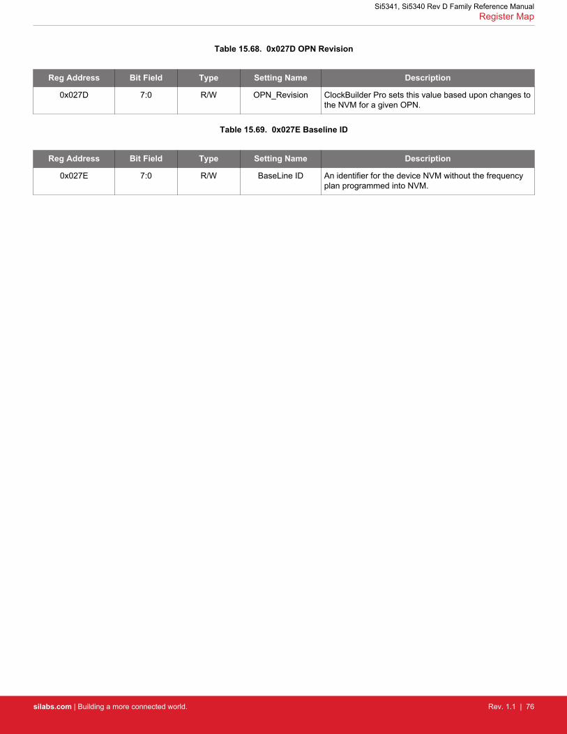
Table 15.68. 0x027D OPN Revision
Reg Address Bit Field Type Setting Name Description
0x027D 7:0 R/W OPN_Revision ClockBuilder Pro sets this value based upon changes tothe NVM for a given OPN.
Table 15.69. 0x027E Baseline ID
Reg Address Bit Field Type Setting Name Description
0x027E 7:0 R/W BaseLine ID An identifier for the device NVM without the frequencyplan programmed into NVM.
Si5341, Si5340 Rev D Family Reference ManualRegister Map
silabs.com | Building a more connected world. Rev. 1.1 | 76
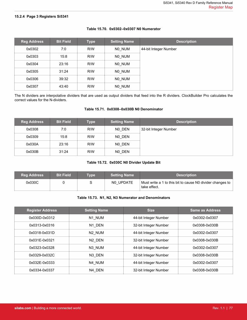
15.2.4 Page 3 Registers Si5341
Table 15.70. 0x0302–0x0307 N0 Numerator
Reg Address Bit Field Type Setting Name Description
0x0302 7:0 R/W N0_NUM 44-bit Integer Number
0x0303 15:8 R/W N0_NUM
0x0304 23:16 R/W N0_NUM
0x0305 31:24 R/W N0_NUM
0x0306 39:32 R/W N0_NUM
0x0307 43:40 R/W N0_NUM
The N dividers are interpolative dividers that are used as output dividers that feed into the R dividers. ClockBuilder Pro calculates thecorrect values for the N-dividers.
Table 15.71. 0x0308–0x030B N0 Denominator
Reg Address Bit Field Type Setting Name Description
0x0308 7:0 R/W N0_DEN 32-bit Integer Number
0x0309 15:8 R/W N0_DEN
0x030A 23:16 R/W N0_DEN
0x030B 31:24 R/W N0_DEN
Table 15.72. 0x030C N0 Divider Update Bit
Reg Address Bit Field Type Setting Name Description
0x030C 0 S N0_UPDATE Must write a 1 to this bit to cause N0 divider changes totake effect.
Table 15.73. N1, N2, N3 Numerator and Denominators
Register Address Setting Name Size Same as Address
0x030D-0x0312 N1_NUM 44-bit Integer Number 0x0302-0x0307
0x0313-0x0316 N1_DEN 32-bit Integer Number 0x0308-0x030B
0x0318-0x031D N2_NUM 44-bit Integer Number 0x0302-0x0307
0x031E-0x0321 N2_DEN 32-bit Integer Number 0x0308-0x030B
0x0323-0x0328 N3_NUM 44-bit Integer Number 0x0302-0x0307
0x0329-0x032C N3_DEN 32-bit Integer Number 0x0308-0x030B
0x032E-0x0333 N4_NUM 44-bit Integer Number 0x0302-0x0307
0x0334-0x0337 N4_DEN 32-bit Integer Number 0x0308-0x030B
Si5341, Si5340 Rev D Family Reference ManualRegister Map
silabs.com | Building a more connected world. Rev. 1.1 | 77
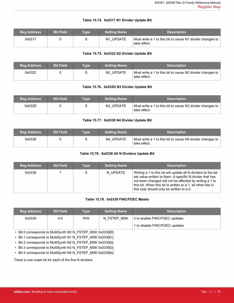
Table 15.74. 0x0317 N1 Divider Update Bit
Reg Address Bit Field Type Setting Name Description
0x0317 0 S N1_UPDATE Must write a 1 to this bit to cause N1 divider changes totake effect.
Table 15.75. 0x0322 N2 Divider Update Bit
Reg Address Bit Field Type Setting Name Description
0x0322 0 S N2_UPDATE Must write a 1 to this bit to cause N2 divider changes totake effect.
Table 15.76. 0x032D N3 Divider Update Bit
Reg Address Bit Field Type Setting Name Description
0x032D 0 S N3_UPDATE Must write a 1 to this bit to cause N3 divider changes totake effect.
Table 15.77. 0x0338 N4 Divider Update Bit
Reg Address Bit Field Type Setting Name Description
0x0338 0 S N4_UPDATE Must write a 1 to this bit to cause N4 divider changes totake effect.
Table 15.78. 0x0338 All N Dividers Update Bit
Reg Address Bit Field Type Setting Name Description
0x0338 1 S N_UPDATE Writing a 1 to this bit will update all N dividers to the lat-est value written to them. A specific N divider that hasnot been changed will not be affected by writing a 1 tothis bit. When this bit is written to a 1, all other bits inthis byte should only be written to a 0.
Table 15.79. 0x0339 FINC/FDEC Masks
Reg Address Bit Field Type Setting Name Description
0x0339 4:0 R/W N_FSTEP_MSK 0 to enable FINC/FDEC updates
1 to disable FINC/FDEC updates
• Bit 0 corresponds to MultiSynth N0 N_FSTEP_MSK 0x0339[0]• Bit 1 corresponds to MultiSynth N1 N_FSTEP_MSK 0x0339[1]• Bit 2 corresponds to MultiSynth N2 N_FSTEP_MSK 0x0339[2]• Bit 3 corresponds to MultiSynth N3 N_FSTEP_MSK 0x0339[3]• Bit 4 corresponds to MultiSynth N4 N_FSTEP_MSK 0x0339[4]
There is one mask bit for each of the five N dividers.
Si5341, Si5340 Rev D Family Reference ManualRegister Map
silabs.com | Building a more connected world. Rev. 1.1 | 78

Table 15.80. 0x033B–0x0340 N0 Frequency Step Word
Reg Address Bit Field Type Setting Name Description
0x033B 7:0 R/W N0_FSTEPW 44-bit Integer Number
0x033C 15:8 R/W N0_FSTEPW
0x033D 23:16 R/W N0_FSTEPW
0x033E 31:24 R/W N0_ FSTEPW
0x033F 39:32 R/W N0_ FSTEPW
0x0340 43:40 R/W N0_ FSTEPW
This is a 44-bit integer value which is directly added (FDEC) or subtracted (FINC) from the Nx_NUM parameter when FINC or FDEC isasserted. ClockBuilder Pro calculates the correct values for the N0 Frequency Step Word. Each N divider has the ability to add or sub-tract up to a 44-bit value. The Nx_NUM register value does not change when an FINC or FDEC is performed so that the starting pointof Nx_NUM is in the Nx_NUM register.
Table 15.81. Frequency Step Word for N1, N2, N3, N4
Register Address Setting Name Size Same as Address
0x0341-0x0346 N1_FSTEPW 44-bit Integer Number 0x033B-0x0340
0x0347-0x034C N2_FSTEPW 44-bit Integer Number 0x033B-0x0340
0x034D-0x0352 N3_FSTEPW 44-bit Integer Number 0x033B-0x0340
0x0353-0x0358 N4_FSTEPW 44-bit Integer Number 0x033B-0x0340
Table 15.82. 0x0359–0x35A N0 Delay Control
Reg Address Bit Field Type Setting Name Description
0x0359 7:0 R/W N0_DELAY[7:0] Lower byte of N0_DELAY[15:0]
0x035A 7:0 R/W N0_DELAY[15:8] Upper byte of N0_DELAY[15:0]
Table 15.83. 0x035B–0x035C Divider N1 Delay Control
Reg Address Bit Field Type Setting Name Description
0x035B 7:0 R/W N1_DELAY[7:0] Lower byte of N1_DELAY[15:0]
0x035C 7:0 R/W N1_DELAY[15:8] Upper byte of N1_DELAY[15:0]
Table 15.84. 0x035D–0x035E Divider N2 Delay Control
Reg Address Bit Field Type Setting Name Description
0x035D 7:0 R/W N2_DELAY[7:0] Lower byte of N2_DELAY[15:0]
0x035E 7:0 R/W N2_DELAY[15:8] Upper byte of N2_DELAY[15:0]
Si5341, Si5340 Rev D Family Reference ManualRegister Map
silabs.com | Building a more connected world. Rev. 1.1 | 79
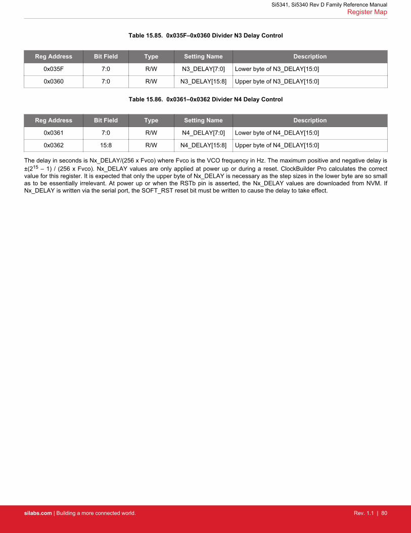
Table 15.85. 0x035F–0x0360 Divider N3 Delay Control
Reg Address Bit Field Type Setting Name Description
0x035F 7:0 R/W N3_DELAY[7:0] Lower byte of N3_DELAY[15:0]
0x0360 7:0 R/W N3_DELAY[15:8] Upper byte of N3_DELAY[15:0]
Table 15.86. 0x0361–0x0362 Divider N4 Delay Control
Reg Address Bit Field Type Setting Name Description
0x0361 7:0 R/W N4_DELAY[7:0] Lower byte of N4_DELAY[15:0]
0x0362 15:8 R/W N4_DELAY[15:8] Upper byte of N4_DELAY[15:0]
The delay in seconds is Nx_DELAY/(256 x Fvco) where Fvco is the VCO frequency in Hz. The maximum positive and negative delay is±(215 – 1) / (256 x Fvco). Nx_DELAY values are only applied at power up or during a reset. ClockBuilder Pro calculates the correctvalue for this register. It is expected that only the upper byte of Nx_DELAY is necessary as the step sizes in the lower byte are so smallas to be essentially irrelevant. At power up or when the RSTb pin is asserted, the Nx_DELAY values are downloaded from NVM. IfNx_DELAY is written via the serial port, the SOFT_RST reset bit must be written to cause the delay to take effect.
Si5341, Si5340 Rev D Family Reference ManualRegister Map
silabs.com | Building a more connected world. Rev. 1.1 | 80

15.2.5 Page 9 Registers Si5341
Table 15.87. 0x090E XAXB Configuration
Reg Address Bit Field Type Setting Name Description
0x090E 0 R/W XAXB_EXTCLK_EN 0 to use a crystal at the XAXB pins
1 to use an external clock source at the XAXB pins. Asingled ended clock must be applied at the XA input.
0x090E 1 R/W XAXB_PDNB 0-Power down the oscillator and buffer circuitry at theXA/XB pins
1- No power down
Table 15.88. 0x091C Enable Zero Delay Mode
Reg Address Bit Field Type Setting Name Description
0x091C 2:0 R/W ZDM_EN 3 = Zero delay mode.
4 = Normal mode.
All other values must not be written.
Table 15.89. 0x0943 Status and Control I/O Voltage Select
Reg Address Bit Field Type Setting Name Description
0x0943 0 R/W IO_VDD_SEL 0 for 1.8 V external connections
1 for 3.3 V external connections
The IO_VDD_SEL configuration bit selects the option of operating the serial interface voltage thresholds from the VDD or the VDDApin. By default the IO_VDD_SEL bit is set to the VDD option. The serial interface pins are always 3.3 V tolerant even when the device'sVDD pin is supplied from a 1.8 V source. When the I2C or SPI host is operating at 3.3 V and the Si5341/40 IO_VDD_SEL = 1.8 V, thehost should write the IO_VDD_SEL configuration bit to the VDDA option. This will ensure that both the host and the serial interface areoperating at the optimum voltage thresholds. The IO_VDD_SEL bit also affects the status pin levels and control pin thresholds. WhenIO_VDD_SEL = 0, the status outputs will have a VOH of ~1.8 V. When IO_VDD_SEL = 1 the status outputs will have a VOH of ~3.3 V.When IO_VDD_SEL=0, the control input pins will have an input threshold based upon the VDD supply voltage of 1.8 V. WhenIO_VDD_SEL=1, the control input pins will have an input threshold based upon the VDDA supply voltage of 3.3 V. See Table 4 andTable 6 of the Si5341/40 data sheet for details.
Table 15.90. 0x0949 Clock Input Control
Reg Address Bit Field Type Setting Name Description
0x0949 3:0 R/W IN_EN Enables for the four inputs clocks, IN0 through FB_IN.
1 to enable, 0 to disable
• Input 0 corresponds to IN_EN 0x0949 [0].• Input 1 corresponds to IN_EN 0x0949 [1].• Input 2 corresponds to IN_EN 0x0949 [2].• FB_IN corresponds to IN_EN 0x0949 [3].
Si5341, Si5340 Rev D Family Reference ManualRegister Map
silabs.com | Building a more connected world. Rev. 1.1 | 81

Table 15.91. 0x094A Input Clock Routing Enable
Reg Address Bit Field Type Setting Name Description
0x094A 6:4 R/W INx_TO_PFD_EN When = 1, enables the routing of the 3 input clocksIN0,1,2 to the Phase Detector. Each bit corresponds tothe inputs as follows [6:4] = [IN2 IN1 IN0]. IN_SEL isused to select the input clock that is applied to thephase detector.
Table 15.92. 0x095E
Reg Address Bit Field Type Setting Name Description
0x095E 0 R/W M_INTEGER
15.2.6 Page A Registers Si5341
Table 15.93. 0x0A03 N Divider Clocks
Reg Address Bit Field Type Setting Name Description
0x0A03 4:0 R/W N_CLK_TO_OUTX_EN
BIts in this field correspond to the N dividers as [N4 N3N2 N1 N0]. If an N divider is used, the corresponding bitmust be 1. See also registers 0x0A05 and 0x0B4A[4:0].
Table 15.94. 0x0A04 N Divider Phase Interpolator Bypass
Reg Address Bit Field Type Setting Name Description
0x0A04 4:0 R/W N_PIBYP Bypasses the Phase Interpolator of the N Multisynth di-vider. Set to a 1 when the value of N divider is integerand will not be used as a DCO. Set to a 0 when the val-ue of N is fractional (used as a DCO). Slightly lower out-put jitter may occur when the Phase Interpolator is by-passed (=1). Bits in this field correspond to the N divid-ers as [N4 N3 N2 N1 N0].
Table 15.95. 0x0A05 N Divider Power Down
Reg Address Bit Field Type Setting Name Description
0x0A05 4:0 R/W N_PDNB Powers down the N divider. If an N divider is not used,set the respective bit to 0 to power it down. Bits in thisfield correspond to the N dividers as [N4 N3 N2 N1 N0].See also registers 0x0A03 and 0x0B4A[4;0].
15.2.7 Page B Registers Si5341
Table 15.96. 0x0B44 Loss of Signal Clock Disable
Reg Address Bit Field Type Setting Name Description
0x0B44 3:0 R/W PDIV_ENB
Si5341, Si5340 Rev D Family Reference ManualRegister Map
silabs.com | Building a more connected world. Rev. 1.1 | 82
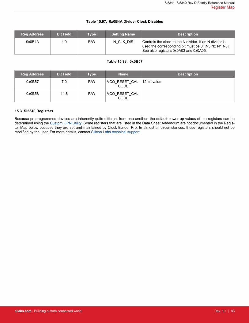
Table 15.97. 0x0B4A Divider Clock Disables
Reg Address Bit Field Type Setting Name Description
0x0B4A 4:0 R/W N_CLK_DIS Controls the clock to the N divider. If an N divider isused the corresponding bit must be 0. [N3 N2 N1 N0].See also registers 0x0A03 and 0x0A05.
Table 15.98. 0x0B57
Reg Address Bit Field Type Name Description
0x0B57 7:0 R/W VCO_RESET_CAL-CODE
12-bit value
0x0B58 11:8 R/W VCO_RESET_CAL-CODE
15.3 Si5340 Registers
Because preprogrammed devices are inherently quite different from one another, the default power up values of the registers can bedetermined using the Custom OPN Utility. Some registers that are listed in the Data Sheet Addendum are not documented in the Regis-ter Map below because they are set and maintained by Clock Builder Pro. In almost all circumstances, these registers should not bemodified by the user. For more details, contact Silicon Labs technical support.
Si5341, Si5340 Rev D Family Reference ManualRegister Map
silabs.com | Building a more connected world. Rev. 1.1 | 83
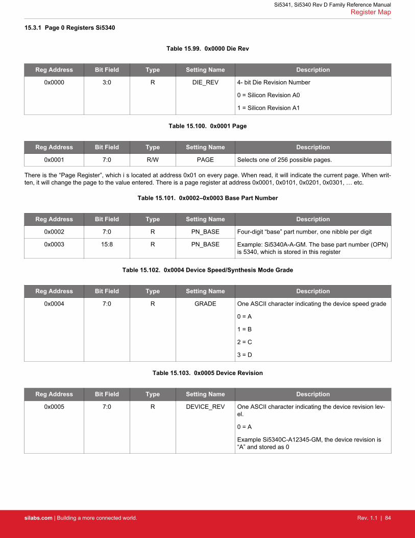
15.3.1 Page 0 Registers Si5340
Table 15.99. 0x0000 Die Rev
Reg Address Bit Field Type Setting Name Description
0x0000 3:0 R DIE_REV 4- bit Die Revision Number
0 = Silicon Revision A0
1 = Silicon Revision A1
Table 15.100. 0x0001 Page
Reg Address Bit Field Type Setting Name Description
0x0001 7:0 R/W PAGE Selects one of 256 possible pages.
There is the “Page Register”, which i s located at address 0x01 on every page. When read, it will indicate the current page. When writ-ten, it will change the page to the value entered. There is a page register at address 0x0001, 0x0101, 0x0201, 0x0301, … etc.
Table 15.101. 0x0002–0x0003 Base Part Number
Reg Address Bit Field Type Setting Name Description
0x0002 7:0 R PN_BASE Four-digit “base” part number, one nibble per digit
Example: Si5340A-A-GM. The base part number (OPN)is 5340, which is stored in this register
0x0003 15:8 R PN_BASE
Table 15.102. 0x0004 Device Speed/Synthesis Mode Grade
Reg Address Bit Field Type Setting Name Description
0x0004 7:0 R GRADE One ASCII character indicating the device speed grade
0 = A
1 = B
2 = C
3 = D
Table 15.103. 0x0005 Device Revision
Reg Address Bit Field Type Setting Name Description
0x0005 7:0 R DEVICE_REV One ASCII character indicating the device revision lev-el.
0 = A
Example Si5340C-A12345-GM, the device revision is“A” and stored as 0
Si5341, Si5340 Rev D Family Reference ManualRegister Map
silabs.com | Building a more connected world. Rev. 1.1 | 84

Table 15.104. 0x0006–0x0008 NVM Identifier
Reg Address Bit Field Type Setting Name Description
0x0006 3:0 R TOOL_VER-SION[3:0]
Special
0x0006 7:4 R TOOL_VER-SION[7:4]
Revision
0x0007 7:0 R TOOL_VER-SION[15:8]
Minor[7:0]
0x0008 0 R TOOL_VER-SION[15:8]
Minor[8]
0x0008 4:1 R TOOL_VER-SION[16]
Major
0x0008 7:5 R TOOL_VER-SION[13:17]
Tool. 0 for Clockbuilder Pro
Table 15.105. 0x0009 Temperature Grade
Reg Address Bit Field Type Setting Name Description
0x0009 7:0 TEMP_GRADE Device temperature grading
0 = Industrial (-40° C to 85° C) ambient conditions
Table 15.106. 0x000A Package ID
Reg Address Bit Field Type Setting Name Description
0x000A 7:0 PKG_ID Package ID
0 = 9x9 mm 64 QFN
1 = 7x7 mm 44 QFN
Part numbers are of the form:
Si<Part Num Base><Grade>-<Device Revision><OPN ID>-<Temp Grade><Package ID>
Examples:
Si5341C-A-12345-GM.
Applies to a “custom” OPN (Ordering Part Number) device. These devices are factory pre-programmed with the frequency plan and allother operating characteristics defined by the user’s ClockBuilder Pro project file.
Si5341C-A-GM.
Applies to a “base” or “blank” OPN device. Base devices are factory pre-programmed to a specific base part type (e.g., Si5341 butexclude any user-defined frequency plan or other user-defined operating characteristics selected in ClockBuilder Pro.
Table 15.107. 0x000B I2C Address
Reg Address Bit Field Type Setting Name Description
0x000B 6:0 R/W I2C_ADDR 7 bit I2C Address
Si5341, Si5340 Rev D Family Reference ManualRegister Map
silabs.com | Building a more connected world. Rev. 1.1 | 85

Table 15.108. 0x000C Status Bits
Reg Address Bit Field Type Setting Name Description
0x000C 0 R SYSINCAL 1 if the device is calibrating.
0x000C 1 R LOSXAXB 1 if there is no signal at the XA pin as the LOS detectoris only connected to the XA pin.
0x000C 2 R LOSREF 1 if the Phase Detector does not have an input fromFB_IN, IN2, IN1, or IN0.
0x000C 3 R LOL 1 if the DSPLL is out of lock.
0x000C 4 R
0x000C 5 R SMB_TMOUT 1 if there is an SMBus timeout error.
Table 15.109. 0x000D INx Loss of Signal (LOS) Alarms
Reg Address Bit Field Type Setting Name Description
0x000D 3:0 R LOSIN 1 if no clock is present at [FB_IN, IN2, IN1, IN0]
Note that each bit corresponds to the input. The LOS bits are not sticky.• Input 0 (IN0) corresponds to LOS at 0x000D [0]• Input 1 (IN1) corresponds to LOS at 0x000D [1]• Input 2 (IN2) corresponds to LOS at 0x000D [2]• FB_IN corresponds to LOS at 0x000D [3]• See also LOSXAXB for LOS at the XAXB input
Table 15.110. 0x0011 Sticky Versions of Status Bits
Reg Address Bit Field Type Setting Name Description
0x0011 0 R SYSINCAL_FLG Sticky version of SYSINCAL. Write a 0 to clear the flag.
0x0011 1 R LOSXAXB_FLG Sticky version of LOSXAXB. Write a 0 to clear the flag.
0x0011 2 R LOSREF_FLG Sticky version of LOSREF. Write a 0 to clear the flag.
0x0011 3 R LOL_FLG Sticky version of LOL. Write a 0 to clear the flag.
0x0011 4 R
0x0011 5 R SMBUS_TIME-OUT_FLG
Sticky version of SMBUS_TIMEOUT. Write a 0 to clearthe flag.
Table 15.111. 0x0012 INx LOS Flags
Reg Address Bit Field Type Setting Name Description
0x0012 3:0 R/W LOSIN_FLG Sticky version of LOS. Write a 0 to clear each individualflag.
Table 15.112. 0x0017 Status Flag Interrupt Masks
Reg Address Bit Field Type Setting Name Description
0x0017 0 R/W SYSIN-CAL_INTR_MSK
1 to mask SYSINCAL_FLG from causing an interrupt
Si5341, Si5340 Rev D Family Reference ManualRegister Map
silabs.com | Building a more connected world. Rev. 1.1 | 86
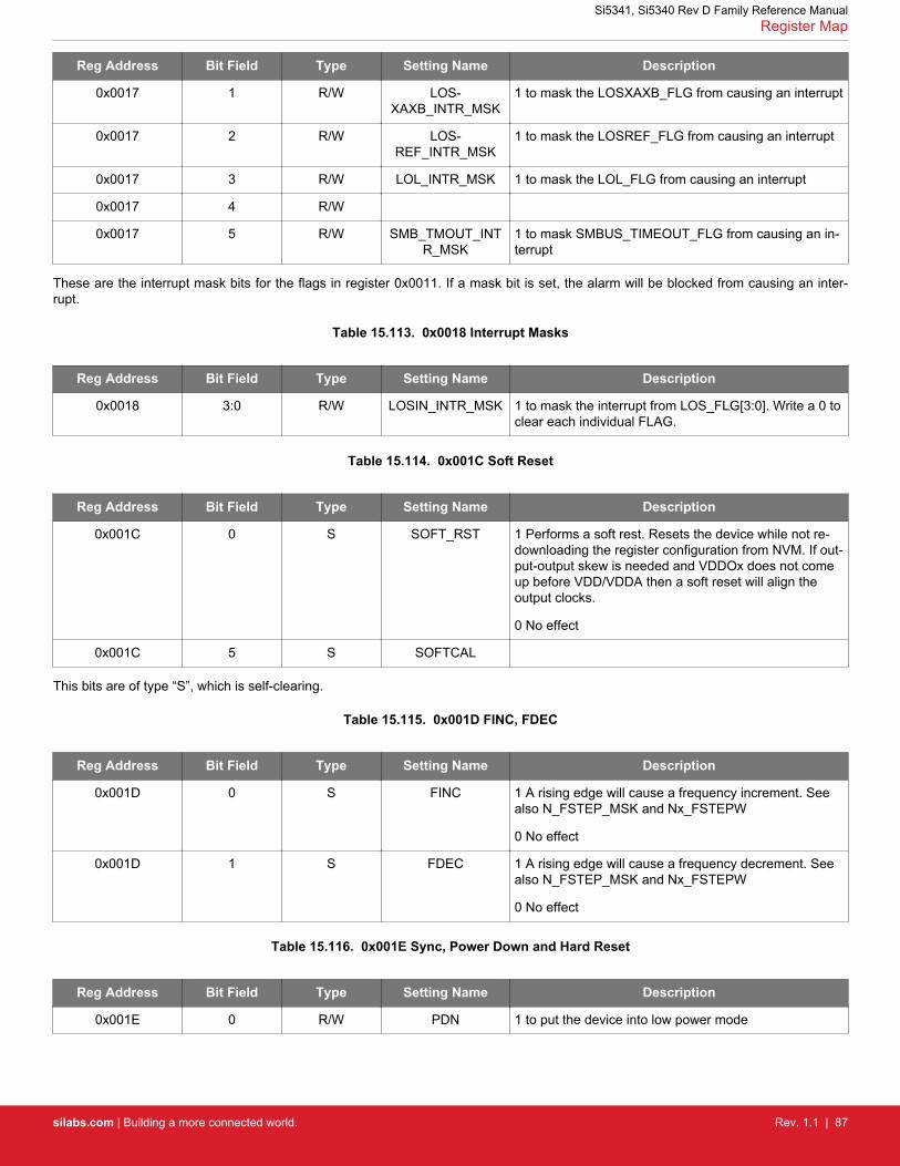
Reg Address Bit Field Type Setting Name Description
0x0017 1 R/W LOS-XAXB_INTR_MSK
1 to mask the LOSXAXB_FLG from causing an interrupt
0x0017 2 R/W LOS-REF_INTR_MSK
1 to mask the LOSREF_FLG from causing an interrupt
0x0017 3 R/W LOL_INTR_MSK 1 to mask the LOL_FLG from causing an interrupt
0x0017 4 R/W
0x0017 5 R/W SMB_TMOUT_INTR_MSK
1 to mask SMBUS_TIMEOUT_FLG from causing an in-terrupt
These are the interrupt mask bits for the flags in register 0x0011. If a mask bit is set, the alarm will be blocked from causing an inter-rupt.
Table 15.113. 0x0018 Interrupt Masks
Reg Address Bit Field Type Setting Name Description
0x0018 3:0 R/W LOSIN_INTR_MSK 1 to mask the interrupt from LOS_FLG[3:0]. Write a 0 toclear each individual FLAG.
Table 15.114. 0x001C Soft Reset
Reg Address Bit Field Type Setting Name Description
0x001C 0 S SOFT_RST 1 Performs a soft rest. Resets the device while not re-downloading the register configuration from NVM. If out-put-output skew is needed and VDDOx does not comeup before VDD/VDDA then a soft reset will align theoutput clocks.
0 No effect
0x001C 5 S SOFTCAL
This bits are of type “S”, which is self-clearing.
Table 15.115. 0x001D FINC, FDEC
Reg Address Bit Field Type Setting Name Description
0x001D 0 S FINC 1 A rising edge will cause a frequency increment. Seealso N_FSTEP_MSK and Nx_FSTEPW
0 No effect
0x001D 1 S FDEC 1 A rising edge will cause a frequency decrement. Seealso N_FSTEP_MSK and Nx_FSTEPW
0 No effect
Table 15.116. 0x001E Sync, Power Down and Hard Reset
Reg Address Bit Field Type Setting Name Description
0x001E 0 R/W PDN 1 to put the device into low power mode
Si5341, Si5340 Rev D Family Reference ManualRegister Map
silabs.com | Building a more connected world. Rev. 1.1 | 87

Reg Address Bit Field Type Setting Name Description
0x001E 1 R/W HARD_RST 1 causes hard reset. The same as power up except thatthe serial port access is not held at reset. NVM is re-downloaded. This does not self-clear, so after settingthe bit it must be cleared.
0 No reset
0x001E 2 S SYNC Logically equivalent to asserting the SYNC pin. Resetsall R dividers to the same state.
Table 15.117. 0x0021 Input Clock Selection
Reg Address Bit Field Type Setting Name Description
0x0021 0 R/W IN_SEL_REGCTRL Selects between register controlled reference clock se-lection and pin controlled clock selection using IN_SEL1and IN_SEL0 pins:
0 for pin controlled clock selection
1 for register clock selection
0x0021 2:1 R/W IN_SEL Selects the reference clock input to the PLL whenIN_SEL_REGCTRL=1.
0 IN0
1 IN1
2 IN2
3 XA/XB
Table 15.118. 0x002B SPI 3 vs 4 Wire
Reg Address Bit Field Type Setting Name Description
0x002B 3 R/W SPI_3WIRE 0 for 4-wire SPI, 1 for 3-wire SPI
Table 15.119. 0x002C LOS Enable
Reg Address Bit Field Type Setting Name Description
0x002C 3:0 R/W LOS_EN 1 to enable LOS for a clock input;
0 for disable
0x002C 4 R/W LOSXAXB_DIS 0 to enable LOS for the XAXB input
1 to disable the LOS for the XAXB input
• Input 0 (IN0): LOS_EN[0]• Input 1 (IN1): LOS_EN[1]• Input 2 (IN2): LOS_EN[2]• FB_IN: LOS_EN[3]
Si5341, Si5340 Rev D Family Reference ManualRegister Map
silabs.com | Building a more connected world. Rev. 1.1 | 88

Table 15.120. 0x002D Loss of Signal Time Value
Reg Address Bit Field Type Setting Name Description
0x002D 1:0 R/W LOS0_VAL_TIME Clock Input 0
0 for 2 msec
1 for 100 msec
2 for 200 msec
3 for one second
0x002D 3:2 R/W LOS1_VAL_TIME Clock Input 1, same as above
0x002D 5:4 R/W LOS2_VAL_TIME Clock Input 2, same as above
0x002D 7:6 R/W LOS3_VAL_TIME Clock Input 3, same as above
When an input clock is gone (and therefore has an active LOS alarm), if the clock returns, there is a period of time that the clock mustbe within the acceptable range before the alarm is removed. This is the LOS_VAL_TIME.
Table 15.121. 0x002E-0x002F LOS0 Trigger Threshold
Reg Address Bit Field Type Setting Name Description
0x002E 7:0 R/W LOS0_TRG_THR 16-bit Threshold Value
0x002F 15:8 R/W LOS0_TRG_THR
ClockBuilder Pro calculates the correct LOS register threshold trigger value for Input 0, given a particular frequency plan.
Table 15.122. 0x0030-0x0031 LOS1 Trigger Threshold
Reg Address Bit Field Type Setting Name Description
0x0030 7:0 R/W LOS1_TRG_THR 16-bit Threshold Value
0x0031 15:8 R/W LOS1_TRG_THR
ClockBuilder Pro calculates the correct LOS register threshold trigger value for Input 1, given a particular frequency plan.
Table 15.123. 0x0032-0x0033 LOS2 Trigger Threshold
Reg Address Bit Field Type Setting Name Description
0x0032 7:0 R/W LOS2_TRG_THR 16-bit Threshold Value
0x0033 15:8 R/W LOS2_TRG_THR
ClockBuilder Pro calculates the correct LOS register threshold trigger value for Input 2, given a particular frequency plan.
Table 15.124. 0x0034-0x0035 LOS3 Trigger Threshold
Reg Address Bit Field Type Setting Name Description
0x0034 7:0 R/W LOS3_TRG_THR 16-bit Threshold Value
0x0035 15:8 R/W LOS3_TRG_THR
ClockBuilder Pro calculates the correct LOS register threshold trigger value for Input 3, given a particular frequency plan.
Si5341, Si5340 Rev D Family Reference ManualRegister Map
silabs.com | Building a more connected world. Rev. 1.1 | 89
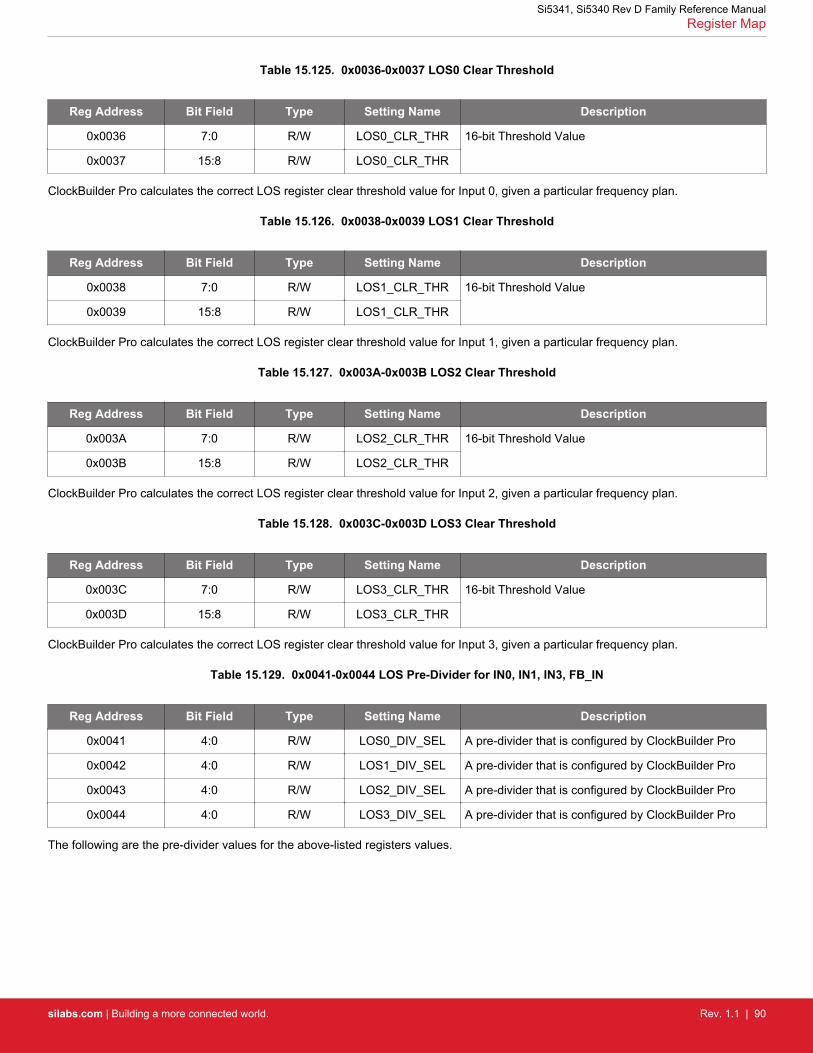
Table 15.125. 0x0036-0x0037 LOS0 Clear Threshold
Reg Address Bit Field Type Setting Name Description
0x0036 7:0 R/W LOS0_CLR_THR 16-bit Threshold Value
0x0037 15:8 R/W LOS0_CLR_THR
ClockBuilder Pro calculates the correct LOS register clear threshold value for Input 0, given a particular frequency plan.
Table 15.126. 0x0038-0x0039 LOS1 Clear Threshold
Reg Address Bit Field Type Setting Name Description
0x0038 7:0 R/W LOS1_CLR_THR 16-bit Threshold Value
0x0039 15:8 R/W LOS1_CLR_THR
ClockBuilder Pro calculates the correct LOS register clear threshold value for Input 1, given a particular frequency plan.
Table 15.127. 0x003A-0x003B LOS2 Clear Threshold
Reg Address Bit Field Type Setting Name Description
0x003A 7:0 R/W LOS2_CLR_THR 16-bit Threshold Value
0x003B 15:8 R/W LOS2_CLR_THR
ClockBuilder Pro calculates the correct LOS register clear threshold value for Input 2, given a particular frequency plan.
Table 15.128. 0x003C-0x003D LOS3 Clear Threshold
Reg Address Bit Field Type Setting Name Description
0x003C 7:0 R/W LOS3_CLR_THR 16-bit Threshold Value
0x003D 15:8 R/W LOS3_CLR_THR
ClockBuilder Pro calculates the correct LOS register clear threshold value for Input 3, given a particular frequency plan.
Table 15.129. 0x0041-0x0044 LOS Pre-Divider for IN0, IN1, IN3, FB_IN
Reg Address Bit Field Type Setting Name Description
0x0041 4:0 R/W LOS0_DIV_SEL A pre-divider that is configured by ClockBuilder Pro
0x0042 4:0 R/W LOS1_DIV_SEL A pre-divider that is configured by ClockBuilder Pro
0x0043 4:0 R/W LOS2_DIV_SEL A pre-divider that is configured by ClockBuilder Pro
0x0044 4:0 R/W LOS3_DIV_SEL A pre-divider that is configured by ClockBuilder Pro
The following are the pre-divider values for the above-listed registers values.
Si5341, Si5340 Rev D Family Reference ManualRegister Map
silabs.com | Building a more connected world. Rev. 1.1 | 90
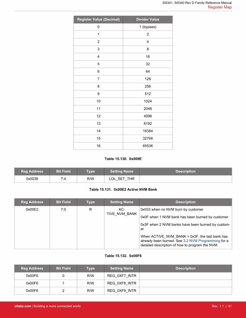
Register Value (Decimal) Divider Value
0 1 (bypass)
1 2
2 4
3 8
4 16
5 32
6 64
7 128
8 256
9 512
10 1024
11 2048
12 4096
13 8192
14 16384
15 32768
16 65536
Table 15.130. 0x009E
Reg Address Bit Field Type Setting Name Description
0x0038 7:4 R/W LOL_SET_THR
Table 15.131. 0x00E2 Active NVM Bank
Reg Address Bit Field Type Setting Name Description
0x00E2 7:0 R AC-TIVE_NVM_BANK
0x033 when no NVM burn by customer
0x0F when 1 NVM bank has been burned by customer
0x3F when 2 NVM banks have been burned by custom-er
When ACTIVE_NVM_BANK = 0x3F, the last bank hasalready been burned. See 3.2 NVM Programming for adetailed description of how to program the NVM.
Table 15.132. 0x00F6
Reg Address Bit Field Type Setting Name Description
0x00F6 0 R/W REG_0XF7_INTR
0x00F6 1 R/W REG_0XF8_INTR
0x00F6 2 R/W REG_0XF9_INTR
Si5341, Si5340 Rev D Family Reference ManualRegister Map
silabs.com | Building a more connected world. Rev. 1.1 | 91

Table 15.133. 0x00F7
Reg Address Bit Field Type Setting Name Description
0x00F7 0 R/W SYSINCAL_INTR
0x00F7 1 R/W LOSXAXB_INTR
0x00F7 2 R/W LOSREF_INTR
0x00F7 3 R/W LOL_INTR
0x00F7 4 R/W LOSVCO_INTR
0x00F7 5 R/W SMBUS_TIME_OUT_INTR
Table 15.134. 0x00F8
Reg Address Bit Field Type Setting Name Description
0x00F8 3:0 R/W LOS_INTR
Si5341, Si5340 Rev D Family Reference ManualRegister Map
silabs.com | Building a more connected world. Rev. 1.1 | 92

15.3.2 Page 1 Registers Si5340
Table 15.135. 0x0102 All Output Clock Driver Disable
Reg Address Bit Field Type Setting Name Description
0x0102 0 R/W OUTALL_DISA-BLE_LOW
0 disables all output drivers
1 no output drivers are disabled by this bit but other sig-nals may disable the outputs.
Table 15.136. 0x0112 Clock Output Driver 0 Configs and Div2 Mode
Reg Address Bit Field Type Setting Name Description
0x0112 0 R/W OUT0_PDN Output driver 0: 0 to power up the driver, 1 to powerdown the driver. Clock outputs will be weakly pulled-low.
0x0112 1 R/W OUT0_OE Output driver 0: 0 to disable the output, 1 to enable theoutput
0x0112 2 R/W OUT0_RDIV_FORCE2
0 R0 divider value is set by R0_REG
1 R0 divider value is forced into divide by 2
Table 15.137. 0x0113 Clock Output Driver 0 Format
Reg Address Bit Field Type Setting Name Description
0x0113 2:0 R/W OUT0_FORMAT 0 Reserved
1 normal differential
2 Low Power differential
3 reserved
4 LVCMOS
5–7 reserved
0x0113 3 R/W OUT0_SYNC_EN 0 disable
1 enable
0x0113 5:4 R/W OUT0_DIS_STATE Determines the state of an output driver when disabled,selectable as
0 disable in low state
1 disable in high state
2 reserved
3 reserved
0x0113 7:6 R/W OUT0_CMOS_DRV LVCMOS output impedance.
Si5341, Si5340 Rev D Family Reference ManualRegister Map
silabs.com | Building a more connected world. Rev. 1.1 | 93

Table 15.138. 0x0114 Output 0 Amplitude and Common Mode Voltage
Reg Address Bit Field Type Setting Name Description
0x0114 3:0 R/W OUT0_CM This field only applies when OUT0_FORMAT=1 or 2.See Table 6.4 Settings for LVDS, LVPECL, and HCSLon page 24 and 16. Appendix A—Setting the Differen-tial Output Driver to Non-Standard Amplitudes for de-tails of the settings.
0x0114 6:4 R/W OUT0_AMPL This field only applies when OUT0_FORMAT=1, 2, or 3.See Table 6.4 Settings for LVDS, LVPECL, and HCSLon page 24 and 16. Appendix A—Setting the Differen-tial Output Driver to Non-Standard Amplitudes for de-tails of the settings when the OUT0_FORMAT=1 or 2.
Table 15.139. 0x0115 Clock Output 0 Mux and Inversion
Reg Address Bit Field Type Setting Name Description
0x0115 2:0 R/W OUT0_MUX_SEL Output driver 0 input mux select.This selects the sourceof the multisynth.
0: N0
1: N1
2: N2
3: N3
4: Reserved
5: Reserved
6: Reserved
7: Reserved
0x0115 3 R/W OUT0_VDD_SEL_EN
0x0115 5:4 R/W OUT0_VDD_SEL
0x0115 7:6 R/W OUT0_INV CLK and CLK not inverted
CLK inverted
CLK and CLK inverted
CLK inverted
Each of the 10 output drivers can be connected to any of the five N dividers. More than 1 output driver can connect to the same Ndivider.
The four output drivers are all identical. The single set of descriptions above for output driver 0 applies to the other three output drivers.
Table 15.140. Registers for OUT1,2,3 as per OUT0 Above
Register Address Description (Same as) Address
0x0117 OUT1_PDN, OUT1_OE, OUT1_RDIV_FORCE2 0x0112
0x0118 OUT1_FORMAT, _SYNC_EN, DIS_STATE, _CMOS_DRV 0x0113
0x0119 OUT1_AMPL, OUT1_CM 0x0114
Si5341, Si5340 Rev D Family Reference ManualRegister Map
silabs.com | Building a more connected world. Rev. 1.1 | 94
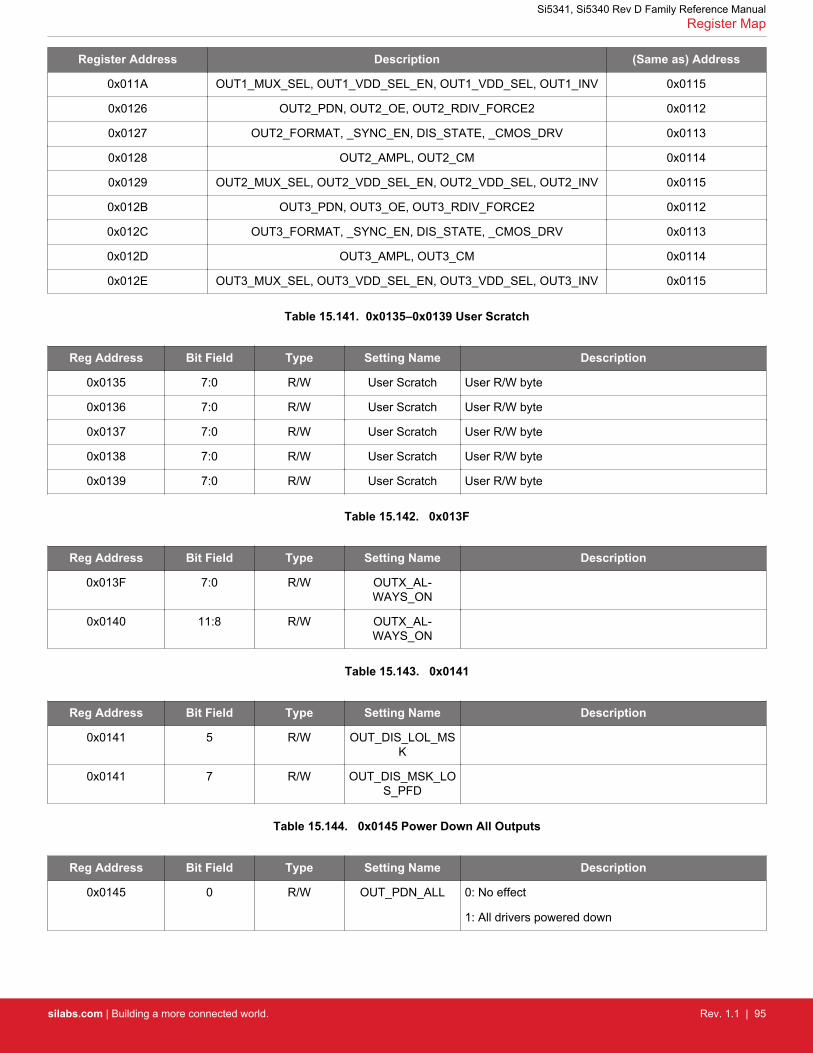
Register Address Description (Same as) Address
0x011A OUT1_MUX_SEL, OUT1_VDD_SEL_EN, OUT1_VDD_SEL, OUT1_INV 0x0115
0x0126 OUT2_PDN, OUT2_OE, OUT2_RDIV_FORCE2 0x0112
0x0127 OUT2_FORMAT, _SYNC_EN, DIS_STATE, _CMOS_DRV 0x0113
0x0128 OUT2_AMPL, OUT2_CM 0x0114
0x0129 OUT2_MUX_SEL, OUT2_VDD_SEL_EN, OUT2_VDD_SEL, OUT2_INV 0x0115
0x012B OUT3_PDN, OUT3_OE, OUT3_RDIV_FORCE2 0x0112
0x012C OUT3_FORMAT, _SYNC_EN, DIS_STATE, _CMOS_DRV 0x0113
0x012D OUT3_AMPL, OUT3_CM 0x0114
0x012E OUT3_MUX_SEL, OUT3_VDD_SEL_EN, OUT3_VDD_SEL, OUT3_INV 0x0115
Table 15.141. 0x0135–0x0139 User Scratch
Reg Address Bit Field Type Setting Name Description
0x0135 7:0 R/W User Scratch User R/W byte
0x0136 7:0 R/W User Scratch User R/W byte
0x0137 7:0 R/W User Scratch User R/W byte
0x0138 7:0 R/W User Scratch User R/W byte
0x0139 7:0 R/W User Scratch User R/W byte
Table 15.142. 0x013F
Reg Address Bit Field Type Setting Name Description
0x013F 7:0 R/W OUTX_AL-WAYS_ON
0x0140 11:8 R/W OUTX_AL-WAYS_ON
Table 15.143. 0x0141
Reg Address Bit Field Type Setting Name Description
0x0141 5 R/W OUT_DIS_LOL_MSK
0x0141 7 R/W OUT_DIS_MSK_LOS_PFD
Table 15.144. 0x0145 Power Down All Outputs
Reg Address Bit Field Type Setting Name Description
0x0145 0 R/W OUT_PDN_ALL 0: No effect
1: All drivers powered down
Si5341, Si5340 Rev D Family Reference ManualRegister Map
silabs.com | Building a more connected world. Rev. 1.1 | 95

15.3.3 Page 2 Registers Si5340
Table 15.145. 0x0202-0x0205 XAXB Frequency Adjust
Reg Address Bit Field Type Setting Name Description
0x0202 7:0 R/W XAXB_FREQ_OFF-SET
32 bit 2’s complement offset adjustment
0x0203 15:8 R/W XAXB_FREQ_OFF-SET
0x0204 23:16 R/W XAXB_FREQ_OFF-SET
0x0205 31:24 R/W XAXB_FREQ_OFF-SET
The clock that is present on XAXB pins is used to create an internal frequency reference for the PLL. The XAXB_FREQ_OFFSET wordis added to the M_NUM to shift the VCO frequency to compensate for a crystal that does not have an 8 pf CL specification. The adjust-ment range is up to ±1000 ppm.
Table 15.146. 0x0206 PXAXB Divider Value
Reg Address Bit Field Type Setting Name Description
0x0206 1:0 R/W PXAXB Sets the value for the divider on the XAXB input.
• 0 = divider value 1• 1 = divider value 2• 2 = divider value 4• 3 = divider value 8
The following registers configure the P-dividers, which are located at the four input clocks seen in Figure 2.2 Si5340 Detailed BlockDiagram on page 11. ClockBuilder Pro calculates the correct values for the P-dividers.
Table 15.147. 0x0208-0x020D P0 Dividers
Reg Address Bit Field Type Setting Name Description
0x0208 7:0 R/W P0
0x0209 15:8 R/W P0
0x020A 23:16 R/W P0
0x020B 31:24 R/W P0
0x020C 39:32 R/W P0
0x020D 47:40 R/W P0
Table 15.148. 0x020E-0x0211 P0 Divider Enable/Set
Reg Address Bit Field Type Setting Name Description
0x020E 7:0 R/W P0_SET
0x020F 15:8 P0_SET
0x0210 23:16 P0_SET
0x0211 31:24 P0_SET
Si5341, Si5340 Rev D Family Reference ManualRegister Map
silabs.com | Building a more connected world. Rev. 1.1 | 96

Table 15.149. 0x0212-0x0217 P1 Dividers
Reg Address Bit Field Type Setting Name Description
0x0212 7:0 R/W P1
0x0213 15:8 R/W P1
0x0214 23:16 R/W P1
0x0215 31:24 R/W P1
0x0216 39:32 R/W P1
0x0217 47:40 R/W P1
Table 15.150. 0x0218-0x021B P1 Divider Enable/Set
Reg Address Bit Field Type Setting Name Description
0x0218 7:0 R/W P1_SET
0x0219 15:8 P1_SET
0x021A 23:16 P1_SET
0x021B 31:24 P1_SET
Table 15.151. 0x021C-0x0221 P2 Dividers
Reg Address Bit Field Type Setting Name Description
0x021C 7:0 R/W P2
0x021D 15:8 R/W P2
0x021E 23:16 R/W P2
0x021F 31:24 R/W P2
0x0220 39:32 R/W P2
0x0221 47:40 R/W P2
Table 15.152. 0x0222-0x0225 P2 Divider Enable/Set
Reg Address Bit Field Type Setting Name Description
0x0222 7:0 R/W P2_SET
0x0223 15:8 P2_SET
0x0224 23:16 P2_SET
0x0225 31:24 P2_SET
Table 15.153. 0x0226-0x022B P3 Dividers
Reg Address Bit Field Type Setting Name Description
0x0226 7:0 R/W P3
0x0227 15:8 R/W P3
Si5341, Si5340 Rev D Family Reference ManualRegister Map
silabs.com | Building a more connected world. Rev. 1.1 | 97
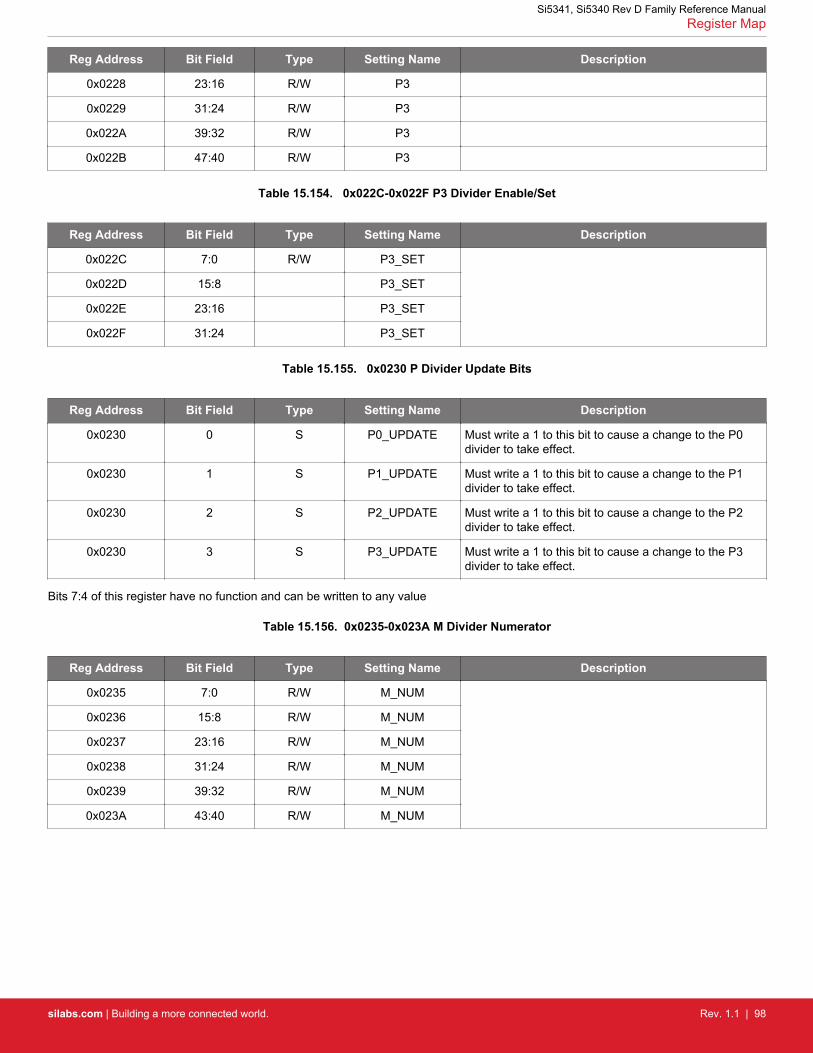
Reg Address Bit Field Type Setting Name Description
0x0228 23:16 R/W P3
0x0229 31:24 R/W P3
0x022A 39:32 R/W P3
0x022B 47:40 R/W P3
Table 15.154. 0x022C-0x022F P3 Divider Enable/Set
Reg Address Bit Field Type Setting Name Description
0x022C 7:0 R/W P3_SET
0x022D 15:8 P3_SET
0x022E 23:16 P3_SET
0x022F 31:24 P3_SET
Table 15.155. 0x0230 P Divider Update Bits
Reg Address Bit Field Type Setting Name Description
0x0230 0 S P0_UPDATE Must write a 1 to this bit to cause a change to the P0divider to take effect.
0x0230 1 S P1_UPDATE Must write a 1 to this bit to cause a change to the P1divider to take effect.
0x0230 2 S P2_UPDATE Must write a 1 to this bit to cause a change to the P2divider to take effect.
0x0230 3 S P3_UPDATE Must write a 1 to this bit to cause a change to the P3divider to take effect.
Bits 7:4 of this register have no function and can be written to any value
Table 15.156. 0x0235-0x023A M Divider Numerator
Reg Address Bit Field Type Setting Name Description
0x0235 7:0 R/W M_NUM
0x0236 15:8 R/W M_NUM
0x0237 23:16 R/W M_NUM
0x0238 31:24 R/W M_NUM
0x0239 39:32 R/W M_NUM
0x023A 43:40 R/W M_NUM
Si5341, Si5340 Rev D Family Reference ManualRegister Map
silabs.com | Building a more connected world. Rev. 1.1 | 98

Table 15.157. 0x023B-0x023E M Divider Denominator
Reg Address Bit Field Type Setting Name Description
0x023B 7:0 R/W M_DEN 32-bit Integer Number
0x023C 15:8 R/W M_DEN
0x023D 23:16 R/W M_DEN
0x023E 31:24 R/W M_DEN
The M-divider numerator and denominator is determined by ClockBuilder Pro for a given frequency plan.
Table 15.158. 0x023F M Divider Update Bit
Reg Address Bit Field Type Setting Name Description
0x023F 0 S M_UPDATE Must write a 1 to this bit to cause M divider changes totake effect.
Bits 7:1 of this register have no function and can be written to any value
Table 15.159. 0x0250-0x0252 R0 Divider
Reg Address Bit Field Type Setting Name Description
0x0250 7:0 R/W R0_REG 24-bit Integer Number. Divide value = (R0_REG+1) x 2
To set R0 = 2, set OUT0_RDIV_FORCE2 = 1, and thenthe R0_REG value is irrelevant. Setting R0_REG=0 willdisable the divider.
0x0251 15:8 R/W R0_REG
0x0252 23:16 R/W R0_REG
The R dividers are with the output drivers and are even integer dividers. The R1–R3 dividers follow the same format as the R0 dividerdescribed above.
Table 15.160. R Dividers for Output 1,2,3
Register Address Setting Name Size Same as Address
0x0253-0x0255 R1_REG 24-bit Integer Number 0x0250-0x0252
0x025C-0x025E R2_REG 24-bit Integer Number 0x0250-0x0252
0x025F-0x0261 R3_REG 24-bit Integer Number 0x0250-0x0252
Si5341, Si5340 Rev D Family Reference ManualRegister Map
silabs.com | Building a more connected world. Rev. 1.1 | 99
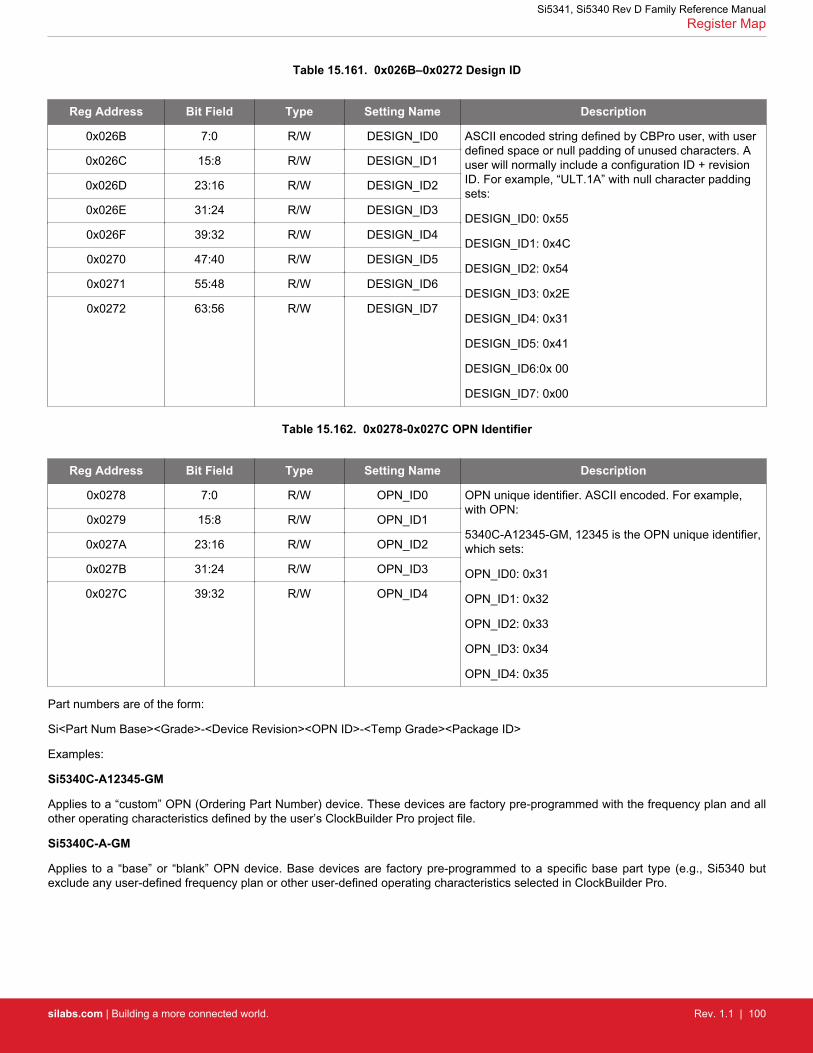
Table 15.161. 0x026B–0x0272 Design ID
Reg Address Bit Field Type Setting Name Description
0x026B 7:0 R/W DESIGN_ID0 ASCII encoded string defined by CBPro user, with userdefined space or null padding of unused characters. Auser will normally include a configuration ID + revisionID. For example, “ULT.1A” with null character paddingsets:
DESIGN_ID0: 0x55
DESIGN_ID1: 0x4C
DESIGN_ID2: 0x54
DESIGN_ID3: 0x2E
DESIGN_ID4: 0x31
DESIGN_ID5: 0x41
DESIGN_ID6:0x 00
DESIGN_ID7: 0x00
0x026C 15:8 R/W DESIGN_ID1
0x026D 23:16 R/W DESIGN_ID2
0x026E 31:24 R/W DESIGN_ID3
0x026F 39:32 R/W DESIGN_ID4
0x0270 47:40 R/W DESIGN_ID5
0x0271 55:48 R/W DESIGN_ID6
0x0272 63:56 R/W DESIGN_ID7
Table 15.162. 0x0278-0x027C OPN Identifier
Reg Address Bit Field Type Setting Name Description
0x0278 7:0 R/W OPN_ID0 OPN unique identifier. ASCII encoded. For example,with OPN:
5340C-A12345-GM, 12345 is the OPN unique identifier,which sets:
OPN_ID0: 0x31
OPN_ID1: 0x32
OPN_ID2: 0x33
OPN_ID3: 0x34
OPN_ID4: 0x35
0x0279 15:8 R/W OPN_ID1
0x027A 23:16 R/W OPN_ID2
0x027B 31:24 R/W OPN_ID3
0x027C 39:32 R/W OPN_ID4
Part numbers are of the form:
Si<Part Num Base><Grade>-<Device Revision><OPN ID>-<Temp Grade><Package ID>
Examples:
Si5340C-A12345-GM
Applies to a “custom” OPN (Ordering Part Number) device. These devices are factory pre-programmed with the frequency plan and allother operating characteristics defined by the user’s ClockBuilder Pro project file.
Si5340C-A-GM
Applies to a “base” or “blank” OPN device. Base devices are factory pre-programmed to a specific base part type (e.g., Si5340 butexclude any user-defined frequency plan or other user-defined operating characteristics selected in ClockBuilder Pro.
Si5341, Si5340 Rev D Family Reference ManualRegister Map
silabs.com | Building a more connected world. Rev. 1.1 | 100

Table 15.163. 0x027D OPN Revision
Reg Address Bit Field Type Setting Name Description
0x27D 7:0 R/W OPN_Revision ClockBuilder Pro sets this value based upon changes tothe NVM for a given OPN.
Table 15.164. 0x027E Baseline ID
Reg Address Bit Field Type Setting Name Description
0x27E 7:0 R/W BaseLine ID An identifier for the device NVM without the frequencyplan programmed into NVM.
Si5341, Si5340 Rev D Family Reference ManualRegister Map
silabs.com | Building a more connected world. Rev. 1.1 | 101
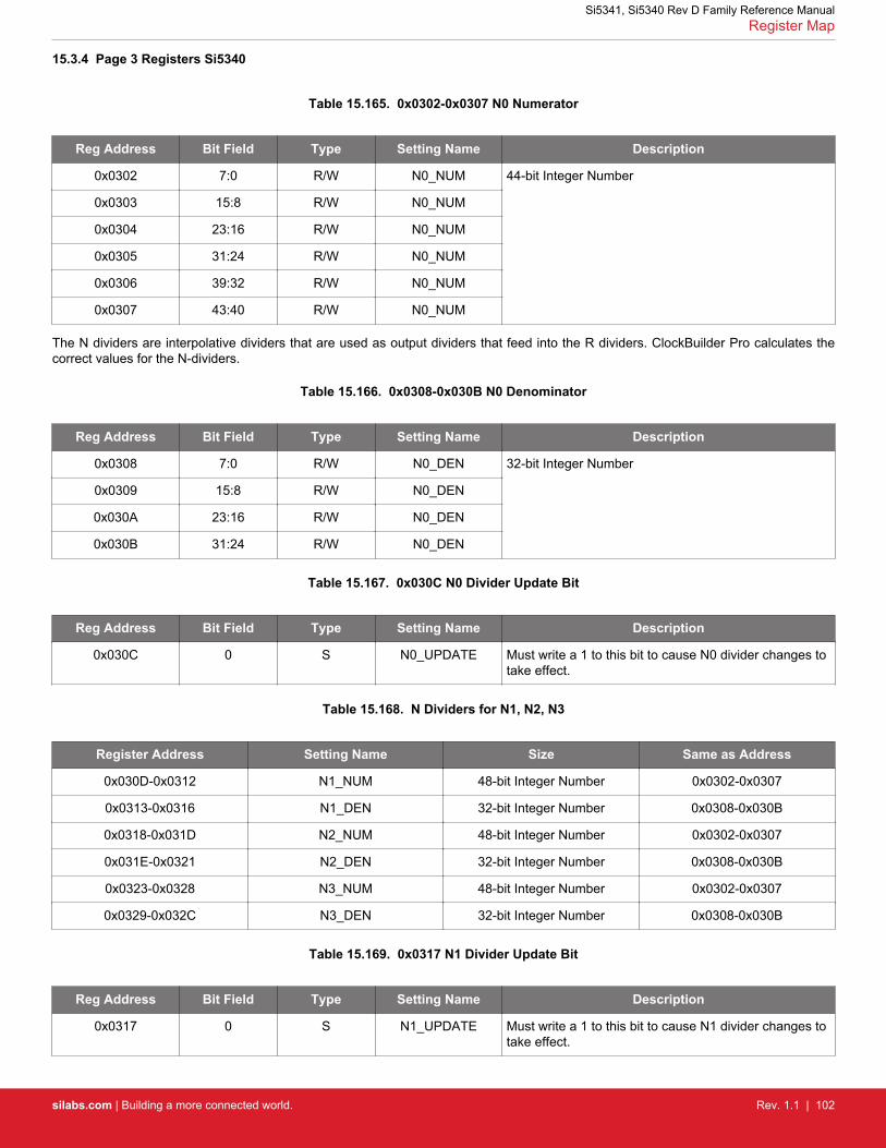
15.3.4 Page 3 Registers Si5340
Table 15.165. 0x0302-0x0307 N0 Numerator
Reg Address Bit Field Type Setting Name Description
0x0302 7:0 R/W N0_NUM 44-bit Integer Number
0x0303 15:8 R/W N0_NUM
0x0304 23:16 R/W N0_NUM
0x0305 31:24 R/W N0_NUM
0x0306 39:32 R/W N0_NUM
0x0307 43:40 R/W N0_NUM
The N dividers are interpolative dividers that are used as output dividers that feed into the R dividers. ClockBuilder Pro calculates thecorrect values for the N-dividers.
Table 15.166. 0x0308-0x030B N0 Denominator
Reg Address Bit Field Type Setting Name Description
0x0308 7:0 R/W N0_DEN 32-bit Integer Number
0x0309 15:8 R/W N0_DEN
0x030A 23:16 R/W N0_DEN
0x030B 31:24 R/W N0_DEN
Table 15.167. 0x030C N0 Divider Update Bit
Reg Address Bit Field Type Setting Name Description
0x030C 0 S N0_UPDATE Must write a 1 to this bit to cause N0 divider changes totake effect.
Table 15.168. N Dividers for N1, N2, N3
Register Address Setting Name Size Same as Address
0x030D-0x0312 N1_NUM 48-bit Integer Number 0x0302-0x0307
0x0313-0x0316 N1_DEN 32-bit Integer Number 0x0308-0x030B
0x0318-0x031D N2_NUM 48-bit Integer Number 0x0302-0x0307
0x031E-0x0321 N2_DEN 32-bit Integer Number 0x0308-0x030B
0x0323-0x0328 N3_NUM 48-bit Integer Number 0x0302-0x0307
0x0329-0x032C N3_DEN 32-bit Integer Number 0x0308-0x030B
Table 15.169. 0x0317 N1 Divider Update Bit
Reg Address Bit Field Type Setting Name Description
0x0317 0 S N1_UPDATE Must write a 1 to this bit to cause N1 divider changes totake effect.
Si5341, Si5340 Rev D Family Reference ManualRegister Map
silabs.com | Building a more connected world. Rev. 1.1 | 102

Table 15.170. 0x0322 N2 Divider Update Bit
Reg Address Bit Field Type Setting Name Description
0x0322 0 S N2_UPDATE Must write a 1 to this bit to cause N2 divider changes totake effect.
Table 15.171. 0x032D N3 Divider Update Bit
Reg Address Bit Field Type Setting Name Description
0x032D 0 S N3_UPDATE Must write a 1 to this bit to cause N3 divider changes totake effect.
Table 15.172. 0x0338 All N Dividers Update Bit
Reg Address Bit Field Type Setting Name Description
0x0338 1 S N_UPDATE Writing a 1 to this bit will update all N dividers to the lat-est value written to them. A specific N divider that hasnot been changed will not be affected by writing a 1 tothis bit. When this bit is written to a 1, all other bits inthis byte should only be written to a 0.
Table 15.173. 0x0339 FINC/FDEC Masks
Reg Address Bit Field Type Setting Name Description
0x0339 3:0 R/W N_FSTEP_MSK 0 to enable FINC/FDEC updates
1 to disable FINC/FDEC updates
• Bit 0 corresponds to MultiSynth N0 N_FSTEP_MSK 0x0339[0]• Bit 1 corresponds to MultiSynth N1 N_FSTEP_MSK 0x0339[1]• Bit 2 corresponds to MultiSynth N2 N_FSTEP_MSK 0x0339[2]• Bit 3 corresponds to MultiSynth N3 N_FSTEP_MSK 0x0339[3]
There is one mask bit for each of the four N dividers.
Table 15.174. 0x033B-0x0340 N0 Frequency Step Word
Reg Address Bit Field Type Setting Name Description
0x033B 7:0 R/W N0_FSTEPW 44-bit Integer Number
0x033C 15:8 R/W N0_FSTEPW
0x033D 23:16 R/W N0_FSTEPW
0x033E 31:24 R/W N0_ FSTEPW
0x033F 39:32 R/W N0_ FSTEPW
0x0340 43:40 R/W N0_ FSTEPW
This is a 44-bit integer value which is directly added (FDEC) or subtracted (FINC) from the Nx_NUM parameter when FINC or FDEC isasserted. ClockBuilder Pro calculates the correct values for the N0 Frequency Step Word. Each N divider has the ability to add or sub-tract up to a 44-bit value. The Nx_NUM register value does not change when an FINC or FDEC is performed so that the starting pointof Nx_NUM is in the Nx_NUM register.
Si5341, Si5340 Rev D Family Reference ManualRegister Map
silabs.com | Building a more connected world. Rev. 1.1 | 103

Table 15.175. Frequency Step Word for N1, N2, N3
Register Address Setting Name Size Same as Address
0x0341–0x0346 N1_FSTEPW 44-bit Integer Number 0x033B–0x0340
0x0347–0x034C N2_FSTEPW 44-bit Integer Number 0x033B–0x0340
0x034D–0x0352 N3_FSTEPW 44-bit Integer Number 0x033B–0x0340
Table 15.176. 0x0359–0x35A N0 Delay Control
Reg Address Bit Field Type Setting Name Description
0x0359 7:0 R/W N0_DELAY[7:0] Lower byte of N0_DELAY[15:0]
0x035A 7:0 R/W N0_DELAY[15:8] Upper byte of N0_DELAY[15:0]
Table 15.177. 0x035B-0x035C Divider N1 Delay Control
Reg Address Bit Field Type Setting Name Description
0x035B 7:0 R/W N1_DELAY[7:0] Lower byte of N1_DELAY[15:0]
0x035C 7:0 R/W N1_DELAY[15:8] Upper byte of N1_DELAY[15:0]
Table 15.178. 0x035D-0x035E Divider N2 Delay Control
Reg Address Bit Field Type Setting Name Description
0x035D 7:0 R/W N2_DELAY[7:0] Lower byte of N2_DELAY[15:0]
0x035E 7:0 R/W N2_DELAY[15:8] Upper byte of N2_DELAY[15:0]
Table 15.179. 0x035F–0x0360 Divider N3 Delay Control
Reg Address Bit Field Type Setting Name Description
0x035F 7:0 R/W N3_DELAY[7:0] Lower byte of N3_DELAY[15:0]
0x0360 7:0 R/W N3_DELAY[15:8] Upper byte of N3_DELAY[15:0]
Nx_DELAY[15:0] is a 2s complement number that sets the output delay of MultiSynths.
The delay in seconds is Nx_DELAY/(256 x Fvco) where Fvco is the VCO frequency in Hz. The maximum positive and negative delay is±(215–1)/(256 x Fvco). Nx_DELAY values are only applied at power up or during a reset. ClockBuilder Pro calculates the correct valuefor this register.
15.3.5 Page 8 Registers Si5340
Table 15.180. 0x0802 FIXREGSA0
Reg Address Bit Field Type Setting Name Description
0x0802 7:0 R/W FIXREGSA0
0x0803 7:0 R/W FIXREGSA0
Si5341, Si5340 Rev D Family Reference ManualRegister Map
silabs.com | Building a more connected world. Rev. 1.1 | 104
Table 15.181. 0x0804 FIXREGSD0
Reg Address Bit Field Type Setting Name Description
0x0804 7:0 R/W FIXREGSD0
Table 15.182. 0x0805 FIXREGSA1
Reg Address Bit Field Type Setting Name Description
0x0805 7:0 R/W FIXREGSA1
0x0806 7:0 R/W FIXREGSA1
Table 15.183. 0x0807 FIXREGSD1
Reg Address Bit Field Type Setting Name Description
0x0807 7:0 R/W FIXREGSD1
Table 15.184. 0x0808 FIXREGSA2
Reg Address Bit Field Type Setting Name Description
0x0808 7:0 R/W FIXREGSA2
0x0809 7:0 R/W FIXREGSA2
Table 15.185. 0x080A FIXREGSD2
Reg Address Bit Field Type Setting Name Description
0x080A 7:0 R/W FIXREGSD2
Table 15.186. 0x080B FIXREGSA3
Reg Address Bit Field Type Setting Name Description
0x080B 7:0 R/W FIXREGSA3
0x080C 7:0 R/W FIXREGSA3
Table 15.187. 0x080D FIXREGSD3
Reg Address Bit Field Type Setting Name Description
0x080D 7:0 R/W FIXREGSD3
Table 15.188. 0x080E FIXREGSA4
Reg Address Bit Field Type Setting Name Description
0x080E 7:0 R/W FIXREGSA4
0x080F 7:0 R/W FIXREGSA4
Si5341, Si5340 Rev D Family Reference ManualRegister Map
silabs.com | Building a more connected world. Rev. 1.1 | 105
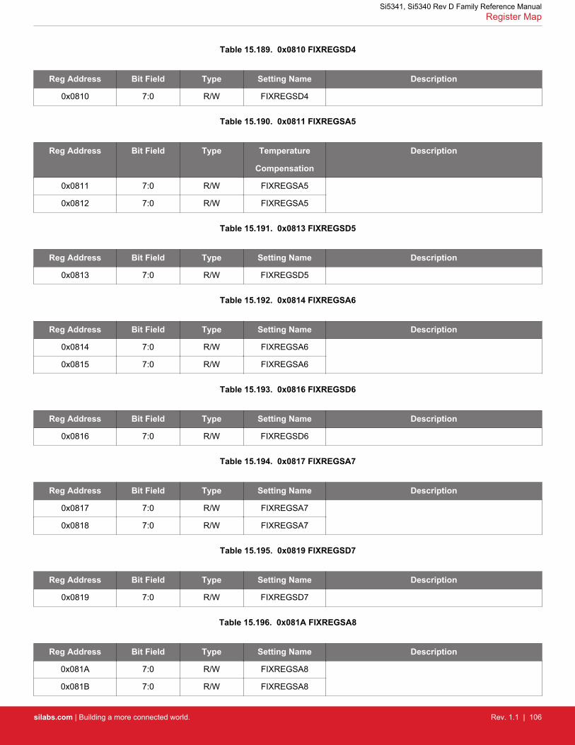
Table 15.189. 0x0810 FIXREGSD4
Reg Address Bit Field Type Setting Name Description
0x0810 7:0 R/W FIXREGSD4
Table 15.190. 0x0811 FIXREGSA5
Reg Address Bit Field Type Temperature
Compensation
Description
0x0811 7:0 R/W FIXREGSA5
0x0812 7:0 R/W FIXREGSA5
Table 15.191. 0x0813 FIXREGSD5
Reg Address Bit Field Type Setting Name Description
0x0813 7:0 R/W FIXREGSD5
Table 15.192. 0x0814 FIXREGSA6
Reg Address Bit Field Type Setting Name Description
0x0814 7:0 R/W FIXREGSA6
0x0815 7:0 R/W FIXREGSA6
Table 15.193. 0x0816 FIXREGSD6
Reg Address Bit Field Type Setting Name Description
0x0816 7:0 R/W FIXREGSD6
Table 15.194. 0x0817 FIXREGSA7
Reg Address Bit Field Type Setting Name Description
0x0817 7:0 R/W FIXREGSA7
0x0818 7:0 R/W FIXREGSA7
Table 15.195. 0x0819 FIXREGSD7
Reg Address Bit Field Type Setting Name Description
0x0819 7:0 R/W FIXREGSD7
Table 15.196. 0x081A FIXREGSA8
Reg Address Bit Field Type Setting Name Description
0x081A 7:0 R/W FIXREGSA8
0x081B 7:0 R/W FIXREGSA8
Si5341, Si5340 Rev D Family Reference ManualRegister Map
silabs.com | Building a more connected world. Rev. 1.1 | 106
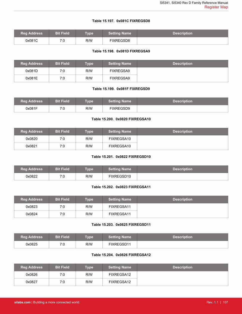
Table 15.197. 0x081C FIXREGSD8
Reg Address Bit Field Type Setting Name Description
0x081C 7:0 R/W FIXREGSD8
Table 15.198. 0x081D FIXREGSA9
Reg Address Bit Field Type Setting Name Description
0x081D 7:0 R/W FIXREGSA9
0x081E 7:0 R/W FIXREGSA9
Table 15.199. 0x081F FIXREGSD9
Reg Address Bit Field Type Setting Name Description
0x081F 7:0 R/W FIXREGSD9
Table 15.200. 0x0820 FIXREGSA10
Reg Address Bit Field Type Setting Name Description
0x0820 7:0 R/W FIXREGSA10
0x0821 7:0 R/W FIXREGSA10
Table 15.201. 0x0822 FIXREGSD10
Reg Address Bit Field Type Setting Name Description
0x0822 7:0 R/W FIXREGSD10
Table 15.202. 0x0823 FIXREGSA11
Reg Address Bit Field Type Setting Name Description
0x0823 7:0 R/W FIXREGSA11
0x0824 7:0 R/W FIXREGSA11
Table 15.203. 0x0825 FIXREGSD11
Reg Address Bit Field Type Setting Name Description
0x0825 7:0 R/W FIXREGSD11
Table 15.204. 0x0826 FIXREGSA12
Reg Address Bit Field Type Setting Name Description
0x0826 7:0 R/W FIXREGSA12
0x0827 7:0 R/W FIXREGSA12
Si5341, Si5340 Rev D Family Reference ManualRegister Map
silabs.com | Building a more connected world. Rev. 1.1 | 107

Table 15.205. 0x0828 FIXREGSD12
Reg Address Bit Field Type Setting Name Description
0x0828 7:0 R/W FIXREGSD12
Table 15.206. 0x0829 FIXREGSA13
Reg Address Bit Field Type Setting Name Description
0x0829 7:0 R/W FIXREGSA13
0x082A 7:0 R/W FIXREGSA13
Table 15.207. 0x082B FIXREGSD13
Reg Address Bit Field Type Setting Name Description
0x082B 7:0 R/W FIXREGSD13
Table 15.208. 0x082C FIXREGSA14
Reg Address Bit Field Type Setting Name Description
0x082C 7:0 R/W FIXREGSA14
0x082D 7:0 R/W FIXREGSA14
Table 15.209. 0x082E FIXREGSD14
Reg Address Bit Field Type Setting Name Description
0x082E 7:0 R/W FIXREGSD14
Table 15.210. 0x082F FIXREGSA15
Reg Address Bit Field Type Setting Name Description
0x082F 7:0 R/W FIXREGSA15
0x0830 7:0 R/W FIXREGSA15
Table 15.211. 0x0831 FIXREGSD15
Reg Address Bit Field Type Setting Name Description
0x0831 7:0 R/W FIXREGSD15
Table 15.212. 0x0832 FIXREGSA16
Reg Address Bit Field Type Setting Name Description
0x0832 7:0 R/W FIXREGSA16
0x0833 7:0 R/W FIXREGSA16
Si5341, Si5340 Rev D Family Reference ManualRegister Map
silabs.com | Building a more connected world. Rev. 1.1 | 108

Table 15.213. 0x0834 FIXREGSD16
Reg Address Bit Field Type Setting Name Description
0x0834 7:0 R/W FIXREGSD16
Table 15.214. 0x0835 FIXREGSA17
Reg Address Bit Field Type Setting Name Description
0x0835 7:0 R/W FIXREGSA17
0x0836 7:0 R/W FIXREGSA17
Table 15.215. 0x0837 FIXREGSD17
Reg Address Bit Field Type Setting Name Description
0x0837 7:0 R/W FIXREGSD17
Table 15.216. 0x0838 FIXREGSA18
Reg Address Bit Field Type Setting Name Description
0x0838 7:0 R/W FIXREGSA18
0x0839 7:0 R/W FIXREGSA18
Table 15.217. 0x083A FIXREGSD18
Reg Address Bit Field Type Setting Name Description
0x083A 7:0 R/W FIXREGSD18
Table 15.218. 0x083B FIXREGSA19
Reg Address Bit Field Type Setting Name Description
0x083B 7:0 R/W FIXREGSA19
0x083C 7:0 R/W FIXREGSA19
Table 15.219. 0x083D FIXREGSD19
Reg Address Bit Field Type Setting Name Description
0x083D 7:0 R/W FIXREGSD19
Table 15.220. 0x083E FIXREGSA20
Reg Address Bit Field Type Setting Name Description
0x083E 7:0 R/W FIXREGSA20
0x083F 7:0 R/W FIXREGSA20
Si5341, Si5340 Rev D Family Reference ManualRegister Map
silabs.com | Building a more connected world. Rev. 1.1 | 109
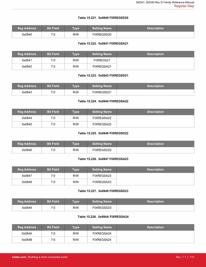
Table 15.221. 0x0840 FIXREGSD20
Reg Address Bit Field Type Setting Name Description
0x0840 7:0 R/W FIXREGSD20
Table 15.222. 0x0841 FIXREGSA21
Reg Address Bit Field Type Setting Name Description
0x0841 7:0 R/W FIXREGS21
0x0842 7:0 R/W FIXREGSA21
Table 15.223. 0x0843 FIXREGSD21
Reg Address Bit Field Type Setting Name Description
0x0843 7:0 R/W FIXREGSD21
Table 15.224. 0x0844 FIXREGSA22
Reg Address Bit Field Type Setting Name Description
0x0844 7:0 R/W FIXREGSA22
0x0845 7:0 R/W FIXREGSA22
Table 15.225. 0x0846 FIXREGSD22
Reg Address Bit Field Type Setting Name Description
0x0846 7:0 R/W FIXREGSD22
Table 15.226. 0x0847 FIXREGSA23
Reg Address Bit Field Type Setting Name Description
0x0847 7:0 R/W FIXREGSA23
0x0848 7:0 R/W FIXREGSA23
Table 15.227. 0x0849 FIXREGSD23
Reg Address Bit Field Type Setting Name Description
0x0849 7:0 R/W FIXREGSD23
Table 15.228. 0x084A FIXREGSA24
Reg Address Bit Field Type Setting Name Description
0x084A 7:0 R/W FIXREGSA24
0x084B 7:0 R/W FIXREGSA24
Si5341, Si5340 Rev D Family Reference ManualRegister Map
silabs.com | Building a more connected world. Rev. 1.1 | 110

Table 15.229. 0x084C FIXREGSD24
Reg Address Bit Field Type Setting Name Description
0x084C 7:0 R/W FIXREGSD24
Table 15.230. 0x084D FIXREGSA25
Reg Address Bit Field Type Setting Name Description
0x084D 7:0 R/W FIXREGSA25
0x084E 7:0 R/W FIXREGSA25
Table 15.231. 0x084F FIXREGSD25
Reg Address Bit Field Type Setting Name Description
0x084F 7:0 R/W FIXREGSD25
Table 15.232. 0x0850 FIXREGSA26
Reg Address Bit Field Type Setting Name Description
0x0850 7:0 R/W FIXREGSA26
0x0851 7:0 R/W FIXREGSA26
Table 15.233. 0x0852 FIXREGSD26
Reg Address Bit Field Type Setting Name Description
0x0852 7:0 R/W FIXREGSD26
Table 15.234. 0x0853 FIXREGSA27
Reg Address Bit Field Type Setting Name Description
0x0853 7:0 R/W FIXREGSA27
0x0854 7:0 R/W FIXREGSA27
Table 15.235. 0x0855 FIXREGSD27
Reg Address Bit Field Type Setting Name Description
0x0855 7:0 R/W FIXREGSD27
Table 15.236. 0x0856 FIXREGSA28
Reg Address Bit Field Type Setting Name Description
0x0856 7:0 R/W FIXREGS28
0x0857 7:0 R/W FIXREGSA28
Si5341, Si5340 Rev D Family Reference ManualRegister Map
silabs.com | Building a more connected world. Rev. 1.1 | 111
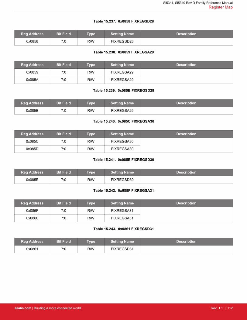
Table 15.237. 0x0858 FIXREGSD28
Reg Address Bit Field Type Setting Name Description
0x0858 7:0 R/W FIXREGSD28
Table 15.238. 0x0859 FIXREGSA29
Reg Address Bit Field Type Setting Name Description
0x0859 7:0 R/W FIXREGSA29
0x085A 7:0 R/W FIXREGSA29
Table 15.239. 0x085B FIXREGSD29
Reg Address Bit Field Type Setting Name Description
0x085B 7:0 R/W FIXREGSA29
Table 15.240. 0x085C FIXREGSA30
Reg Address Bit Field Type Setting Name Description
0x085C 7:0 R/W FIXREGSA30
0x085D 7:0 R/W FIXREGSA30
Table 15.241. 0x085E FIXREGSD30
Reg Address Bit Field Type Setting Name Description
0x085E 7:0 R/W FIXREGSD30
Table 15.242. 0x085F FIXREGSA31
Reg Address Bit Field Type Setting Name Description
0x085F 7:0 R/W FIXREGSA31
0x0860 7:0 R/W FIXREGSA31
Table 15.243. 0x0861 FIXREGSD31
Reg Address Bit Field Type Setting Name Description
0x0861 7:0 R/W FIXREGSD31
Si5341, Si5340 Rev D Family Reference ManualRegister Map
silabs.com | Building a more connected world. Rev. 1.1 | 112
15.3.6 Page 9 Registers Si5340
Table 15.244. 0x090E XAXB Configuration
Reg Address Bit Field Type Setting Name Description
0x090E 0 R/W XAXB_EXTCLK_EN 0 to use a crystal at the XAXB pins
1 to use an external clock source at the XAXB pins
A single ended clock must be applied at the XA input.
0x090E 1 R/W XAXB_PDNB 0-Power down the oscillator and buffer circuitry at theXA/XB pins
1- No power down
Table 15.245. 0x091C Enable Zero Delay Mode
Reg Address Bit Field Type Setting Name Description
0x091C 2:0 R/W ZDM_EN 3 = Zero delay mode.
4 = Normal mode.
All other values must not be written.
Table 15.246. 0x0943 Status and Control I/O Voltage Select
Reg Address Bit Field Type Setting Name Description
0x0943 0 R/W IO_VDD_SEL 0 for 1.8 V external connections
1 for 3.3 V external connections
The IO_VDD_SEL configuration bit selects the option of operating the serial interface voltage thresholds from the VDD or the VDDApin. By default the IO_VDD_SEL bit is set to the VDD option. The serial interface pins are always 3.3 V tolerant even when the device'sVDD pin is supplied from a 1.8 V source. When the I2C or SPI host is operating at 3.3 V and the Si5341/40 IO_VDD_SEL = 1.8 V, thehost must write the IO_VDD_SEL configuration bit to the VDDA option. This will ensure that both the host and the serial interface areoperating at the optimum voltage thresholds. The IO_VDD_SEL bit also affects the status pin levels and control pin thresholds. WhenIO_VDD_SEL = 0, the status outputs will have a VOH of ~1.8 V. When IO_VDD_SEL = 1 the status outputs will have a VOH of ~3.3 V.When IO_VDD_SEL = 0, the control input pins will have an input threshold based upon the VDD supply voltage of 1.8 V. WhenIO_VDD_SEL = 1, the control input pins will have an input threshold based upon the VDDA supply voltage of 3.3 V. The IO_VDD_SELbit has no effect on the LOL or LOSXAXB pins VOH or VOL. See Table 4 and Table 6 of the Si5341/40 data sheet for details.
Table 15.247. 0x0949 Clock Input Control
Reg Address Bit Field Type Setting Name Description
0x0949 3:0 R/W IN_EN Enables for the four inputs clocks, IN0 through FB_IN.
1 to enable, 0 to disable
0x0949 7:4 R/W IN_PULSED_CMOS_EN
• Input 0 corresponds to IN_EN 0x0949 [0]• Input 1 corresponds to IN_EN 0x0949 [1]• Input 2 corresponds to IN_EN 0x0949 [2]• FB_IN corresponds to IN_EN 0x0949 [3]
Si5341, Si5340 Rev D Family Reference ManualRegister Map
silabs.com | Building a more connected world. Rev. 1.1 | 113
Table 15.248. 0x094A Input Clock Routing Enable
Reg Address Bit Field Type Setting Name Description
0x094A 6:4 R/W INx_TO_PFD_EN When = 1, enables the routing of the 3 input clocksIN0,1,2 to the Phase Detector. Each bit corresponds tothe inputs as follows [6:4] = [IN2 IN1 IN0]. IN_SEL isused to select the input clock that is applied to thephase detector.
Table 15.249. 0x095E
Reg Address Bit Field Type Setting Name Description
0x095E 0 R/W M_INTEGER
15.3.7 Page A Registers Si5340
Table 15.250. 0x0A03 N Divider Clocks
Reg Address Bit Field Type Setting Name Description
0x0A03 3:0 R/W N_CLK_TO_OUTX_EN
Bits in this field correspond to the N dividers as [N3 N2N1 N0]. If an N divider is used, the corresponding bitmust be 1. See also registers 0x0A05 and 0x0B4A[3:0].
Table 15.251. 0x0A04 N Divider Phase Interpolator Bypass
Reg Address Bit Field Type Setting Name Description
0x0A04 3:0 R/W N_PIBYP Bypasses the Phase Interpolator of the N Multisynth di-vider. Set to a 1 when the value of the N divider is inte-ger and will not be used as a DCO. Set to a 0 when thevalue of N is fractional (used as a DCO). Slightly loweroutput jitter may occur when the Phase Interpolator isbypassed (=1). Bits in this field correspond to the N di-viders as [N3 N2 N1 N0].
Table 15.252. 0x0A05 N Divider Power Down
Reg Address Bit Field Type Setting Name Description
0x0A05 3:0 R/W N_PDNB Powers down the N divider. If an N divider is not used,set the respective bit to 0 to power it down. Bits in thisfield correspond to the N dividers as [N3 N2 N1 N0].
Si5341, Si5340 Rev D Family Reference ManualRegister Map
silabs.com | Building a more connected world. Rev. 1.1 | 114

15.3.8 Page B Registers Si5340
Table 15.253. 0x0B44
Reg Address Bit Field Type Setting Name Description
0x0B44 3:0 R/W PDIV_ENB
Table 15.254. 0x0B4A Divider Clock Disables
Reg Address Bit Field Type Setting Name Description
0x0B4A 4:0 R/W N_CLK_DIS Controls the clock to the N divider. If an N divider isused the corresponding bit must be 0. [N3 N2 N1 N0].See also registers 0x0A03 and 0x0A05.
Table 15.255. 0x0B57
Reg Address Bit Field Type Name Description
0x0B57 7:0 R/W VCO_RESET_CAL-CODE
12-bit value
0x0B58 11:8 R/W VCO_RESET_CAL-CODE
Appendix A—Setting the Differential Output Driver to Non-Standard Amplitudes
In some applications it may be desirable to have larger or smaller differential amplitudes than produced by the standard LVPECL andLVDS settings, as selected by CBPro. In these cases, the following information describes how to implement these amplitudes by writingto the OUTx_CM and OUTx_AMPL setting names. Contact Silicon Labs for assistance if you want your custom configured device to beprogrammed for any of the settings in this appendix.
The differential output driver has a variable output amplitude capability and 2 basic formats, normal and low power format. The differ-ence between these two formats is that the normal format has an output impedance of ~100 ohms differential and the low power formathas an output impedance of > 500 ohms differential. Note that the rise/fall time is slower when using the Low Power Differential Format.See the Si5341/40 data sheet for the rise/fall time specifications.
If the standard LVDS or LVPECL compatible output amplitudes will not work for a particular application, the variable amplitude capabili-ty can be used to achieve higher or lower amplitudes. For example, a “CML” format is sometimes desired for an application. However,CML is not a defined standard and hence the amplitude of a CML signal for one receiver may be different than that of another receiver.
When the output amplitude needs to be different than standard LVDS or LVPECL, the Common Mode Voltage settings must be set asshown in Table 15.256 Output Differential Common Mode Voltage Settings on page 115. No settings other than the ones in Table15.256 Output Differential Common Mode Voltage Settings on page 115 are supported as the signal integrity could be compromised.In addition the output driver should be AC coupled to the load so that the common mode voltage of the driver is not affected by the load.
Table 15.256. Output Differential Common Mode Voltage Settings
VDDOx(Volts)
Differential Format
OUTx_FORMAT Common Mode Voltage(Volts)
OUTx_CM
3.3 Normal 0x1 2.0 0xB
3.3 Low Power 0x2 1.6 0x7
2.5 Normal 0x1 1.3 0xC
2.5 Low Power 0x2 1.1 0xA
1.8 Normal 0x1 0.8 0xD
Si5341, Si5340 Rev D Family Reference ManualRegister Map
silabs.com | Building a more connected world. Rev. 1.1 | 115

VDDOx(Volts)
Differential Format
OUTx_FORMAT Common Mode Voltage(Volts)
OUTx_CM
1.8 Low Power 0x2 0.8 0xD
The differential amplitude can be set as shown in Table 15.257 Typical Differential Amplitudes on page 116.
Table 15.257. Typical Differential Amplitudes
OUTx_AMPL Normal Differential Format(Vpp SE mV–Typical)
Low Power Differential Format
(Vpp SE mV – Typical)
0 130 200
1 230 400
2 350 620
3 450 820
4 575 1010
5 700 1200
6 810 13501
7 920 16001
1. In low power mode and VDDOx=1.8V, OUTx_AMPL may not be set to 6 or 7.2. These amplitudes are based upon a 100 ohm differential termination.
See the register map portion of this document for additional information about OUTx_FORMAT, OUTx_CM and OUTx_AMPL. ContactSilicon Labs for assistance at https://www.silabs.com/support/pages/contacttechnicalsupport.aspx if you require a factory-programmeddevice to be configured for any of the output driver settings in this appendix.
Si5341, Si5340 Rev D Family Reference ManualRegister Map
silabs.com | Building a more connected world. Rev. 1.1 | 116
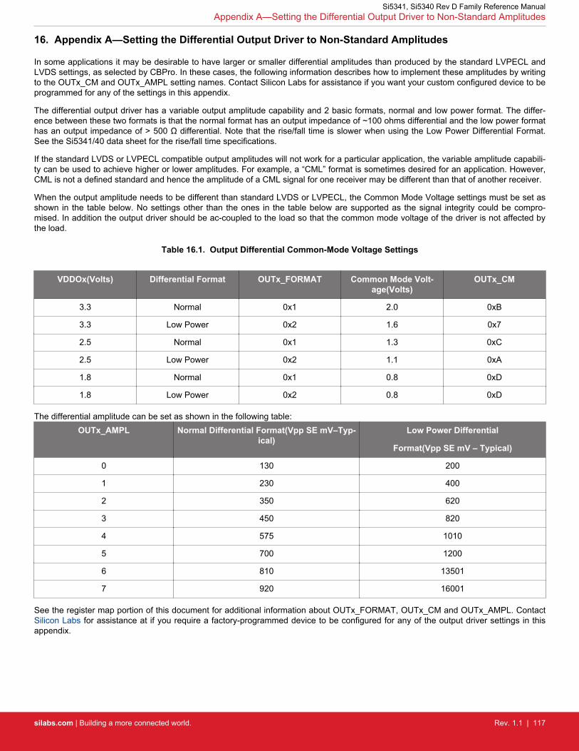
16. Appendix A—Setting the Differential Output Driver to Non-Standard Amplitudes
In some applications it may be desirable to have larger or smaller differential amplitudes than produced by the standard LVPECL andLVDS settings, as selected by CBPro. In these cases, the following information describes how to implement these amplitudes by writingto the OUTx_CM and OUTx_AMPL setting names. Contact Silicon Labs for assistance if you want your custom configured device to beprogrammed for any of the settings in this appendix.
The differential output driver has a variable output amplitude capability and 2 basic formats, normal and low power format. The differ-ence between these two formats is that the normal format has an output impedance of ~100 ohms differential and the low power formathas an output impedance of > 500 Ω differential. Note that the rise/fall time is slower when using the Low Power Differential Format.See the Si5341/40 data sheet for the rise/fall time specifications.
If the standard LVDS or LVPECL compatible output amplitudes will not work for a particular application, the variable amplitude capabili-ty can be used to achieve higher or lower amplitudes. For example, a “CML” format is sometimes desired for an application. However,CML is not a defined standard and hence the amplitude of a CML signal for one receiver may be different than that of another receiver.
When the output amplitude needs to be different than standard LVDS or LVPECL, the Common Mode Voltage settings must be set asshown in the table below. No settings other than the ones in the table below are supported as the signal integrity could be compro-mised. In addition the output driver should be ac-coupled to the load so that the common mode voltage of the driver is not affected bythe load.
Table 16.1. Output Differential Common-Mode Voltage Settings
VDDOx(Volts) Differential Format OUTx_FORMAT Common Mode Volt-age(Volts)
OUTx_CM
3.3 Normal 0x1 2.0 0xB
3.3 Low Power 0x2 1.6 0x7
2.5 Normal 0x1 1.3 0xC
2.5 Low Power 0x2 1.1 0xA
1.8 Normal 0x1 0.8 0xD
1.8 Low Power 0x2 0.8 0xD
The differential amplitude can be set as shown in the following table:OUTx_AMPL Normal Differential Format(Vpp SE mV–Typ-
ical)Low Power Differential
Format(Vpp SE mV – Typical)
0 130 200
1 230 400
2 350 620
3 450 820
4 575 1010
5 700 1200
6 810 13501
7 920 16001
See the register map portion of this document for additional information about OUTx_FORMAT, OUTx_CM and OUTx_AMPL. ContactSilicon Labs for assistance at if you require a factory-programmed device to be configured for any of the output driver settings in thisappendix.
Si5341, Si5340 Rev D Family Reference ManualAppendix A—Setting the Differential Output Driver to Non-Standard Amplitudes
silabs.com | Building a more connected world. Rev. 1.1 | 117

17. Document Change List
Revision 1.0
July 2016, initial release.
Revision 1.1
Updated Dynamic PLL Section.
Si5341, Si5340 Rev D Family Reference ManualDocument Change List
silabs.com | Building a more connected world. Rev. 1.1 | 118

http://www.silabs.com
Silicon Laboratories Inc.400 West Cesar ChavezAustin, TX 78701USA
ClockBuilder ProOne-click access to Timing tools, documentation, software, source code libraries & more. Available for Windows and iOS (CBGo only).
www.silabs.com/CBPro
Timing Portfoliowww.silabs.com/timing
SW/HWwww.silabs.com/CBPro
Qualitywww.silabs.com/quality
Support and Communitycommunity.silabs.com
DisclaimerSilicon Labs intends to provide customers with the latest, accurate, and in-depth documentation of all peripherals and modules available for system and software implementers using or intending to use the Silicon Labs products. Characterization data, available modules and peripherals, memory sizes and memory addresses refer to each specific device, and "Typical" parameters provided can and do vary in different applications. Application examples described herein are for illustrative purposes only. Silicon Labs reserves the right to make changes without further notice and limitation to product information, specifications, and descriptions herein, and does not give warranties as to the accuracy or completeness of the included information. Silicon Labs shall have no liability for the consequences of use of the information supplied herein. This document does not imply or express copyright licenses granted hereunder to design or fabricate any integrated circuits. The products are not designed or authorized to be used within any Life Support System without the specific written consent of Silicon Labs. A "Life Support System" is any product or system intended to support or sustain life and/or health, which, if it fails, can be reasonably expected to result in significant personal injury or death. Silicon Labs products are not designed or authorized for military applications. Silicon Labs products shall under no circumstances be used in weapons of mass destruction including (but not limited to) nuclear, biological or chemical weapons, or missiles capable of delivering such weapons.
Trademark InformationSilicon Laboratories Inc.® , Silicon Laboratories®, Silicon Labs®, SiLabs® and the Silicon Labs logo®, Bluegiga®, Bluegiga Logo®, Clockbuilder®, CMEMS®, DSPLL®, EFM®, EFM32®, EFR, Ember®, Energy Micro, Energy Micro logo and combinations thereof, "the world’s most energy friendly microcontrollers", Ember®, EZLink®, EZRadio®, EZRadioPRO®, Gecko®, ISOmodem®, Micrium, Precision32®, ProSLIC®, Simplicity Studio®, SiPHY®, Telegesis, the Telegesis Logo®, USBXpress®, Zentri and others are trademarks or registered trademarks of Silicon Labs. ARM, CORTEX, Cortex-M3 and THUMB are trademarks or registered trademarks of ARM Holdings. Keil is a registered trademark of ARM Limited. All other products or brand names mentioned herein are trademarks of their respective holders.


![WELCOME! [d2y1pz2y630308.cloudfront.net] · 4/15/2018 · Pastor, Rev. Joseph C. Lee Parochial Vicar, Rev. Eugene Okoli Adult & Family Director, Richard Johnson x23 Adult & Family](https://img.pdfslide.us/doc/110x75/5f9470b9ec38f8631935114c/welcome-4152018-pastor-rev-joseph-c-lee-parochial-vicar-rev-eugene.jpg)