Embed Size (px)
Citation preview
Freescale SemiconductorProduct Brief
Document Number: MPC5668xPBRev. 1, 03/2008
Contents
This document contains preview information on a new
product that may be in a design phase or under development. Freescale reserves the right to
change or discontinue this product without notice.
Application Examples . . . . . . . . . . . . . . . . . . . . . . . . . . . . 21.1 Gateway Controller Application Example . . . . . . . . 2Features . . . . . . . . . . . . . . . . . . . . . . . . . . . . . . . . . . . . . . 32.1 MPC5668G/E Features . . . . . . . . . . . . . . . . . . . . . . 32.2 MPC5668G Block Diagram . . . . . . . . . . . . . . . . . . . 62.3 MPC5668E Block Diagram . . . . . . . . . . . . . . . . . . . 72.4 Critical Performance Parameters. . . . . . . . . . . . . . . 82.5 Packages. . . . . . . . . . . . . . . . . . . . . . . . . . . . . . . . . 92.6 Module Features . . . . . . . . . . . . . . . . . . . . . . . . . . . 9Developer Environment . . . . . . . . . . . . . . . . . . . . . . . . . . 23
MPC5668G/E Family Product Brief32-bit MCU family built on the Power Architecture™ embedded category for automotive gateway and high end body applications
The MPC5668G/E is a new family of next generation microcontrollers built on the Power Architecture embedded category. This document describes the features of the device and potential options available within the planned family members, and highlights important characteristics of the device. This is a preliminary document for a product that is still in development. Its purpose is to communicate information on the intended features of the family members. Information contained within this document is subject to change without notice.
The MPC5668G/E family of 32-bit microcontrollers is the latest achievement in integrated automotive application controllers. It belongs to an expanding family of automotive-focused products designed to address the next wave of gateway and body controller applications within the vehicle. The advanced and cost-efficient host processor core of the MPC5668G/E automotive controller family complies with the Power Architecture embedded category, which is 100 percent user-mode compatible with the original PowerPC user instruction
1
2
3
© Freescale Semiconductor, Inc., 2008. All rights reserved.
Freescale Confidential Proprietary, NDA RequiredPreliminary—Subject to Change Without Notice
Application Examples
set architecture (UISA). It operates at speeds of up to 128 MHz and offers high performance processing optimized for high end communication gateway controllers. It capitalizes on the available development infrastructure of current Power Architecture devices and will be supported with software drivers, operating systems and configuration code to assist with users implementations. Refer to Section 3, “Developer Environment,” for more information.
The MPC5668G/E has two levels of memory hierarchy, a 32 KB unified cache and 592/128 KB on-chip L2 SRAM. 2 MB of internal flash is also provided. Refer to Table 1 for specific memory and feature sets of the proposed family members.
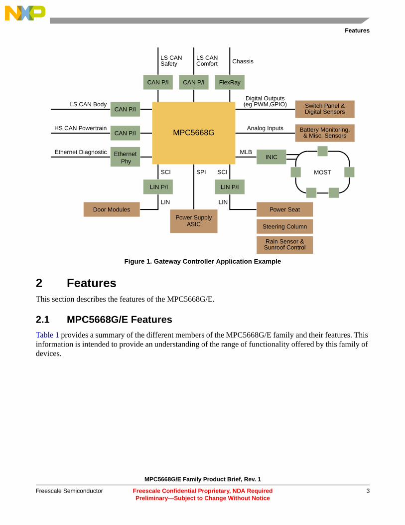
1 Application ExamplesThe MPC5668G/E is designed to address the next wave of high performance gateway and body controllers applications within the vehicle. As shown in the following examples, the MCU is central to the application and provides the flexibility to add or remove peripheral components in a modular design.
1.1 Gateway Controller Application ExampleGateway controller modules primarily control the inter-bus communications necessary to pass information between the multiple communications busses with in the vehicle:
• CAN communications—dominant vehicle bus within automotive• FlexRay— high bandwidth bus used to support time critical communications for safety related
network communications with redundancy and high bandwidth data transfer• MOST— high bandwidth multimedia communications on MOST ring• Ethernet— diagnostics and vehicle programing• LIN— low bandwidth sub-bus communications• Body control — combined internal cabin control such as lighting or redundant operation for BCM
functions
Figure 1 shows the MPC5668G/E used in an example gateway controller application.
MPC5668G/E Family Product Brief, Rev. 1
Freescale Confidential Proprietary, NDA RequiredPreliminary—Subject to Change Without Notice
Freescale Semiconductor2
Features
Figure 1. Gateway Controller Application Example
2 FeaturesThis section describes the features of the MPC5668G/E.
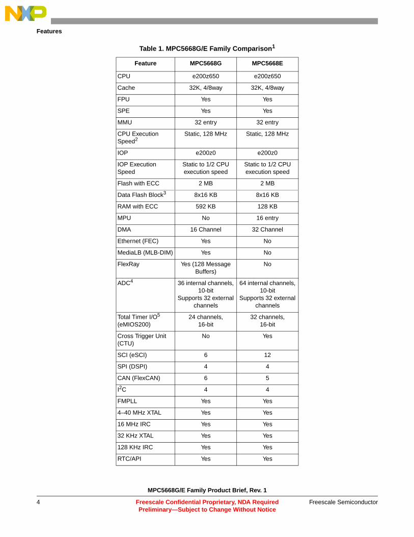
2.1 MPC5668G/E FeaturesTable 1 provides a summary of the different members of the MPC5668G/E family and their features. This information is intended to provide an understanding of the range of functionality offered by this family of devices.
MPC5668G
Digital Outputs
SCI SCI
LS CAN Body
HS CAN Powertrain
Ethernet Diagnostic
LIN LIN
(eg PWM,GPIO)
Analog Inputs
SPI
MLB
MOST
LS CANSafety
LS CANComfort Chassis
CAN P/I CAN P/I FlexRay
CAN P/I
CAN P/I
Ethernet
LIN P/I LIN P/I
Door ModulesPower Supply
ASIC
Power Seat
Steering Column
Rain Sensor &Sunroof Control
INIC
Battery Monitoring,& Misc. Sensors
Switch Panel &Digital Sensors
Phy
MPC5668G/E Family Product Brief, Rev. 1
Freescale Confidential Proprietary, NDA RequiredPreliminary—Subject to Change Without Notice
Freescale Semiconductor 3
Features
Table 1. MPC5668G/E Family Comparison1
Feature MPC5668G MPC5668E
CPU e200z650 e200z650
Cache 32K, 4/8way 32K, 4/8way
FPU Yes Yes
SPE Yes Yes
MMU 32 entry 32 entry
CPU Execution Speed2
Static, 128 MHz Static, 128 MHz
IOP e200z0 e200z0
IOP Execution Speed
Static to 1/2 CPU execution speed
Static to 1/2 CPU execution speed
Flash with ECC 2 MB 2 MB
Data Flash Block3 8x16 KB 8x16 KB
RAM with ECC 592 KB 128 KB
MPU No 16 entry
DMA 16 Channel 32 Channel
Ethernet (FEC) Yes No
MediaLB (MLB-DIM) Yes No
FlexRay Yes (128 Message Buffers)
No
ADC4 36 internal channels, 10-bit
Supports 32 external channels
64 internal channels, 10-bit
Supports 32 external channels
Total Timer I/O5
(eMIOS200)24 channels,
16-bit 32 channels,
16-bit
Cross Trigger Unit (CTU)
No Yes
SCI (eSCI) 6 12
SPI (DSPI) 4 4
CAN (FlexCAN) 6 5
I2C 4 4
FMPLL Yes Yes
4–40 MHz XTAL Yes Yes
16 MHz IRC Yes Yes
32 KHz XTAL Yes Yes
128 KHz IRC Yes Yes
RTC/API Yes Yes
MPC5668G/E Family Product Brief, Rev. 1
Freescale Confidential Proprietary, NDA RequiredPreliminary—Subject to Change Without Notice
Freescale Semiconductor4
Features
PIT 8 8
STM Yes Yes
WDOG (SWT) Yes Yes
GPIO6 155 155
Clock Monitor (PLL) Yes Yes
Interrupt Controller (INTC)
Yes Yes
Boot Assist Module (BAM)
Yes Yes
System Integration Unit (SIU)
Yes Yes
JTAG Yes Yes
Nexus Debug(Only supported on emulation package)
Nexus3 (e200Z6)Nexus2+ (e200Z0)
Nexus3 (e200Z6)Nexus2+ (e200Z0)
ProductionPackage
208 MAPBGA 208 MAPBGA
Emulation Package
256 MAPBGA 256 MAPBGA
NOTES:1 Feature set dependent on selected peripheral multiplexing.2 Based on 105°C ambient operating temperature 3 Data Flash included within main Flash array memory size 4 Depends on pin muxing5 Refer to Section 2.6.16, “Enhanced Modular Input Output System
(eMIOS200),” for information on the channel configuration and functions
6 Estimated I/O count for proposed packages based on multiplexing with peripherals.
Table 1. MPC5668G/E Family Comparison1 (continued)
Feature MPC5668G MPC5668E
MPC5668G/E Family Product Brief, Rev. 1
Freescale Confidential Proprietary, NDA RequiredPreliminary—Subject to Change Without Notice
Freescale Semiconductor 5
Features
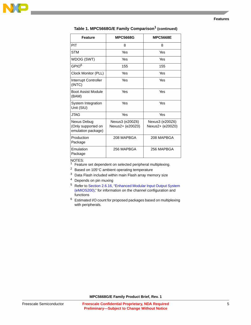
2.2 MPC5668G Block DiagramFigure 2 shows a top-level block diagram of the MPC5668G family.
Figure 2. MPC5668G Block Diagram
ADC – Analog to Digital ConverterBAM – Boot Assist ModuleDSPI – Serial Peripherals InterfaceECC – Error Correction CodeeMIOS – Timed Input OutputeDMA – Enhanced Direct Memory Access controllereSCI – Serial Communications InterfaceFEC – Fast Ethernet ControllerFlexCAN – Controller Area Network controllerFlexRay™ – FlexRay Bus Controller
4–40 MHz
SPP Crossbar Switch (XBAR)
FMPLLe200z650 Core
32K Cache
16ChDMA
16 MHz
FPU/SPE
VLE
MMU(32TLB)
LEGEND
e200z0 Core
VLE
MASTERS
Mux
Flash(ECC)
SRAM(ECC)
512 KB2 MB
AIPS(0) BridgeB
6 x eSCI
36 x ADC
2 x I2C
2 x DSPI
24 x eMIOS 6 x FlexCAN
JTAG
NDINexus3(Z6)
DEBUG
NDINexus2+(Z0)
AIPS(1) Bridge A
2 x I2C
2 x DSPI
VREG
4/8 WayFEC MLB-DIM FlexRay
ControllerIRCXTALMPC5668G
Standby RAM
SRAM(ECC)
80 KB
FMPLL – Frequency Modulated Phase Locked LoopI2C – Inter IC ControllerINTC – Interrupt ControllerJTAG – Joint Test Action Group interfaceMLB-DIM – Media Local Bus Device Interface ModuleNDI – Nexus Debug InterfacePIT – Periodic Interrupt TimerRTC – Real Time ClockSIU – System IntegrationSTM – System Timer ModuleSWT – Software Watchdog Timer
128 kHzIRC
32 KHzXTAL
SWT
INTC
SIU
PIT
BAM
RTC/API
STM
MPC5668G/E Family Product Brief, Rev. 1
Freescale Confidential Proprietary, NDA RequiredPreliminary—Subject to Change Without Notice
Freescale Semiconductor6
Features
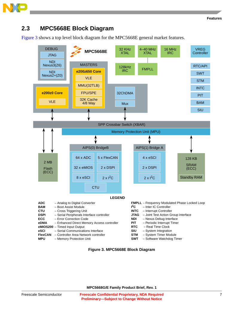
2.3 MPC5668E Block DiagramFigure 3 shows a top level block diagram for the MPC5668E general market features.
Figure 3. MPC5668E Block Diagram
FMPLL – Frequency Modulated Phase Locked LoopI2C – Inter IC ControllerINTC – Interrupt ControllerJTAG – Joint Test Action Group interfaceNDI – Nexus Debug InterfacePIT – Periodic Interrupt TimerRTC – Real Time ClockSIU – System IntegrationSTM – System Timer ModuleSWT – Software Watchdog Timer
ADC – Analog to Digital ConverterBAM – Boot Assist ModuleCTU – Cross Triggering UnitDSPI – Serial Peripherals Interface controllerECC – Error Correction CodeeDMA – Enhanced Direct Memory Access controllereMIOS200 – Timed Input OutputeSCI – Serial Communications InterfaceFlexCAN – Controller Area Network controllerMPU – Memory Protection Unit
4–40 MHz
SPP Crossbar Switch (XBAR)
FMPLLe200z650 Core
32K Cache
32ChDMA
16 MHz
128kHz
FPU/SPE
VLE
MMU(32TLB)
LEGEND
32 KHz
e200z0 Core
VLE
MASTERS
Mux
Memory Protection Unit (MPU)
Flash(ECC)
SRAM(ECC)
128 KB2 MB
AIPS(0) BridgeB
64 x ADC
32 x eMIOS
5 x FlexCAN
2 x DSPI
8 x eSCI
CTU
2 x I2C
JTAG
NDINexus3(Z6)
DEBUG
NDINexus2+(Z0)
AIPS(1) Bridge A
4 x eSCI
2 x I2C
2 x DSPI
SWT
VREG
INTC
SIU
PIT
BAM
RTC/API
STM
4/8 Way
ControllerIRCXTAL XTAL
IRC
MPC5668E
Standby RAM
MPC5668G/E Family Product Brief, Rev. 1
Freescale Confidential Proprietary, NDA RequiredPreliminary—Subject to Change Without Notice
Freescale Semiconductor 7
Features
2.4 Critical Performance ParametersThe critical performance parameters of the MPC5668G/E feature the following:
• Fully static design operation up to a maximum of 128 MHz, based on 105°C ambient• Temperature range –40° to 105° C ambient temperature• Low power design
— Designed for dynamic power management of core and peripherals— Software-controlled clock gating of peripherals— Simple power domains to minimize leakage in low power modes— Internal voltage regulator (VREG) enables operation with a single input voltage — 5 V(nominal) to 3.3 V(nominal) continuous range— External Ballast control
• ADC analog supply ranges 3.3 V±10% and 5 V ±10%• Low voltage detect circuit implemented• Cold crank support• Several I/O pins can be supplied from independent input supplies in the range 3.3 V – 5 V
(nominal)• Separate MLB I/O pin supply domain down to 2.5 V nominal• Configurable pins
— Selectable pull-up, pull-down, or no pull on all GPIO pins— Selectable open-drain pin
2.4.1 Low Power Operation
The MPC5668G/E has one dynamic power mode and one static power mode:• Low-power modes use clock gating to halt the clock for all or part of the device• The lowest power mode also uses power gating to automatically turn off the power supply to parts
of the device to minimize leakage• Dynamic power mode: RUN
— RUN mode is the main operating mode where the entire device is powered and clocked and where most processing activity is done
• Static power mode: SLEEP— SLEEP mode halts the clock to the entire device and turns off the power to the majority of the
chip in order to offer the lowest power consumption mode of the MPC5668G/E. In SLEEP mode the contents of the cores, on-chip peripheral registers and part of the volatile memory are not held. The device can be awakened from up to 32 I/O pins, a reset, or from an internal periodic wake-up. It is also possible to enable the 16 MHz IRC, the 4–40 MHz XTAL, 128 KHz IRC and the 32 KHz XTAL.– SLEEP1 mode retains 32 KB of the on-chip RAM– SLEEP2 mode retains the 64 KB of the on-chip RAM
MPC5668G/E Family Product Brief, Rev. 1
Freescale Confidential Proprietary, NDA RequiredPreliminary—Subject to Change Without Notice
Freescale Semiconductor8
Features
– SLEEP3 mode retains 128 KB of the on-chip RAM— Fast wake-up using the on-chip 16 MHz IRC allows rapid execution from RAM on exit from
low power modes– In SLEEP mode, a 4–40 MHz XTAL can be enabled to continue to run – In SLEEP mode, the 16 MHz IRC can be enabled to continue to run and may be selected to
clock the RTC and API– In SLEEP mode, the 128 KHz IRC can be enabled to run and may be selected to clock the
RTC and API– In Sleep mode the 32 KHz XTAL can be enabled to run and may be selected to clock the
RTC and API• Up to 32 external pins for wake-up from low power modes• Input filters available on all wake-up pins to minimize false wakeups due to noise• Rapid exit from low power mode with fast startup internal voltage regulator
2.5 Packages MPC5668G/E family members are offered in the following package types:
• 208-ball MAPBGA, 1mm ball pitch, 17mm × 17mm outline for production• 256-ball MAPBGA 1mm ball pitch 17mm × 17mm outline for emulation (not available for
production)
2.6 Module FeaturesThe following sections provide details of the modules implemented on the MPC5668G/E.
2.6.1 High Performance e200z650 Core Processor(CPU)
32-bit CPU built on Power Architecture technology• Freescale Variable Length Encoding (VLE) enhancements for code size footprint reduction• Thirty-two 64-bit general-purpose registers (GPRs)• Memory management unit (MMU) with 32-entry fully-associative translation look-aside buffer
(TLB)• Branch processing unit• Fully pipelined load/store unit• 32 KB unified cache with line locking
— 4/8-way set associative— Two 32-bit fetches per clock— Eight-entry store buffer— Way locking— Supports assigning cache as instruction or data only on a per way basis— Supports tag and data parity
MPC5668G/E Family Product Brief, Rev. 1
Freescale Confidential Proprietary, NDA RequiredPreliminary—Subject to Change Without Notice
Freescale Semiconductor 9
Features
• Vectored interrupt support• Very low interrupt latency• Reservation instructions for implementing read-modify-write constructs (internal SRAM and
flash)• Signal processing engine (SPE) auxiliary processing unit (APU) operating on 64-bit general
purpose registers• Floating point
— IEEE® 754 compatible with software wrapper— Single precision in hardware; double precision with software library— Conversion instructions between single precision floating point and fixed point
• Wait instruction• Extensive system development support through Nexus debug module
2.6.2 I/O Processor High Performance e200z0 Core (IOP)
The IOP supports the following features:• High performance, low cost e200z0 core processor for managing peripherals and interrupts• Single issue 4-stage pipelined in-order execution, 32-bit Power Architecture™ CPU• Variable length encoding (VLE), allowing mixed 16-bit and 32-bit instructions
— Results in efficient code size footprint— Minimizes impact on performance
• Branch processing acceleration using lookahead instruction buffer• Load/store unit
— 1-cycle load latency— Misaligned access support— No load-to-use pipeline bubbles
• Thirty-two 32-bit general purpose registers (GPRs)• Hardware vectored interrupt support• Reservation instructions for implementing read-modify-write constructs• Multi-cycle divide (divw) and load multiple (lmw) store multiple (smw) multiple class
instructions, can be interrupted to prevent increases in interrupt latency• Extensive system development support through Nexus debug port
2.6.3 On-Chip Voltage Regulator (VREG)
The on-chip voltage regulator includes the following features:• Single supply device• Continuous 3.3 V to 5 V (+10%, –5%) input supply voltage supported• Supports I/O levels independent of main supply
MPC5668G/E Family Product Brief, Rev. 1
Freescale Confidential Proprietary, NDA RequiredPreliminary—Subject to Change Without Notice
Freescale Semiconductor10
Features
— MLB has separate supply pins to support down to 2.5 V (nominal) operation— Multiple I/O domains with separate supply pins
• Low voltage detectors (LVD) supported on internal supplies• Cold crank operation supported without triggering LVDs
2.6.4 Enhanced Direct Memory Access Controller (eDMA)
The following summarizes the MPC5668G/E implementation of the eDMA controller:• Support independent 8, 16 or 32 bit single value or block transfers• Supports variable sized queues and circular queues• Source and destination address registers are independently configured to post-increment or remain
constant• Each transfer is initiated by a peripheral, CPU, periodic timer interrupt or eDMA channel request• Each eDMA channel can optionally send an interrupt request to the CPU on completion of a single
value or block transfer• DMA transfers possible between system memories, SPI’s, I2C, ADC, eSCI, eMIOS200 and
General Purpose I/O’s• Programmable DMA channel mux allows assignment of any DMA source to any available DMA
channel with up to a total of 64 potential request sources.
2.6.5 Fast Ethernet Controller (FEC)
The FEC incorporates the following features• Support for 3 different physical interfaces
— 100 Mbps IEEE 802.3 MII— 10 Mbps IEEE 802.3 MII— 10 Mbps 7-wire interface (industry standard)
• Built in FIFO and DMA controller• IEEE 802.3 MAC (compliant with IEEE 802.3 1998 edition)• Programmable max frame length supports IEEE 802.1 VLAN tags and priority• IEEE 802.3 full duplex flow control• Support for full duplex operation (200 Mbps throughput) with a system clock of 100 MHz using
the external TX_CLK or RX_CLK• Support for full duplex operation(100 Mbps throughput) with a system clock of 50 MHz using the
external TX_CLK or RX_CLK• Retransmission from transmit FIFO following a collision (no system bus utilization)• Automatic internal flushing of the receive FIFO for runts (collision fragments) and address
recognition rejects(no system bus utilization)• Address recognition• RMON and IEEE statistics
MPC5668G/E Family Product Brief, Rev. 1
Freescale Confidential Proprietary, NDA RequiredPreliminary—Subject to Change Without Notice
Freescale Semiconductor 11
Features
• Interrupts for network activity and error conditions
2.6.6 Media Local Bus (MLB)
The following summarizes the MLB configuration:• Support of 16 logical channels running at a maximum speed of 1024 Fs• Transmission of commands and data and reception of receive status when functioning as the
transmitting device associated with a logical channel address• Reception of commands and data and transmission as receive status responses when functioning
as the receiving device associated with a logical channel address• System channel command handling• Internal DMA operation• Local channel buffer RAM (single port RAM) size of 2048 × 36 bits words• Support for 3-pin only• Support for MLB I/O voltage specs 2.5 V (nominal) and 3.3 V(nominal)
2.6.7 Crossbar Switch (XBAR)
The following summarizes the MPC5668G/E implementation of the crossbar switch:• Up to 6 master ports
— Masters: Z6 CPU, Z0 CPU, eDMA, FlexRay, FEC, MLB• Multiple bus slaves to enable access to flash, SRAM ports and peripherals• Multiple AIPS bridges to support connection to all peripheral modules• Crossbar supports consecutive transfers from master to available slaves• 32-bit internal address bus, 32-bit internal data bus• User configurable priority arbitration based for masters• Temporary dynamic priority elevation for IOP and DMA
2.6.8 Memory Protection Unit (MPU)
The MLB provides the following features:• Supports up to 16 region descriptors for per-master protection• Start and end address defined with 32-byte granularity• Overlapping regions supported• Protection attributes can optionally include process ID• Protection offered for 4 concurrent read ports• Read and write attributes for all masters• Execute and supervisor/user mode attributes for processor masters
MPC5668G/E Family Product Brief, Rev. 1
Freescale Confidential Proprietary, NDA RequiredPreliminary—Subject to Change Without Notice
Freescale Semiconductor12
Features
2.6.9 Interrupt Controller (INTC)
The MPC5668G/E implements an interrupt controller that features the following:• Unique 9-bit vector for each of the 288 separate interrupt sources• 8 software triggerable interrupt sources• 16 priority levels with fixed hardware arbitration within priority levels for each interrupt source• Ability to modify the ISR or task priority.
— Modifying the priority can be used to implement the priority ceiling protocol for accessing shared resources.
• External high priority interrupt directly accessing the main core critical interrupt mechanism• Interrupt steering between main CPU and IOP
— Independent selection of any interrupt source to be routed through IOP— Interrupts share same priority level between IOP and CPU
2.6.10 System Clocks and Clock Generation
The following list summarizes the system clock and clock generation on the MPC5668G/E:• System clock can be derived from the following sources
— 4–40 MHz XTAL— FMPLL— 16 MHz IRC oscillator
• Programmable output clock divider of system clock (÷1, ÷2, ÷4, ÷8)• Separate programmable peripheral bus clock divider ratio (÷1, ÷2, ÷4, ÷8) applied to system clock• Frequency Modulated Phase-locked loop (FMPLL)
— Input clock frequency from 4 MHz to 40 MHz— Clock source from external oscillator— Lock detect circuitry continuously monitors lock status— Loss of clock (LOC) detection for reference and feedback clocks— On-chip loop filter (for improved electomagnetic interference performance and reduces
number of external components required)• On-chip crystal oscillator supporting 4 MHz to 40 MHz crystals• Dedicated 16 MHz internal RC oscillator
— 16 MHz internal RC oscillator supports low speed code execution and clocking of peripherals through selection as the system clock
— Used as default clock source out of reset— Provides a clock for rapid start-up from low power modes— Provides a back-up clock in the event of PLL or external oscillator clock failure— 5% accuracy over the operating temperature range (after factory trim)— Trimming registers to support frequency adjustment with in-application calibration
MPC5668G/E Family Product Brief, Rev. 1
Freescale Confidential Proprietary, NDA RequiredPreliminary—Subject to Change Without Notice
Freescale Semiconductor 13
Features
• Dedicated internal 128 KHz internal RC oscillator for low power mode operation, self wake-up and watchdog— 5% accuracy (after factory trim)— Trimming registers to support improve accuracy with in-application calibration
• Dedicated 32 KHz external oscillator for accurate timed wake-up
2.6.11 System Integration Unit (SIU)
The SIU features the following:• Up to four levels of internal pin muliplexing, allowing exceptional flexibility in the allocation of
device functions for each package• Centralized general purpose input output (GPIO) control of up to 155 input/output pins (package
dependent)• All GPIO pins can be independently configured to support pull-up, pull down, or no pull• Reading and writing to GPIO supported both as individual pins and 16-bit wide ports• The majority of the peripheral pins can be alternatively configured as both general purpose input
or output pins. The exception is selected precision ADC channels which support alternative configuration as general purpose inputs only.
• Direct readback of the pin value supported on all digital output pins through the SIU• Configurable digital input filter that can be applied to up to 32 general purpose input pins for noise
elimination on external wakeups
2.6.12 Software Watchdog Timer (SWT)
The Watchdog on the MPC5668G/E features the following:• Watchdog enabled out of reset with default 10 ms timeout from internal 128 KHz IRC clock• Supports normal and windowed mode• Support for protected access to watchdog control registers with optional soft and hard locks
— Soft lock allows the lock to be overridden by writing a special software code — Hard lock prevents any changes until after a reset, once enabled
• Watchdog supports optional halting during low power modes• Configurable response on timeout: reset, interrupt, or interrupt followed by reset
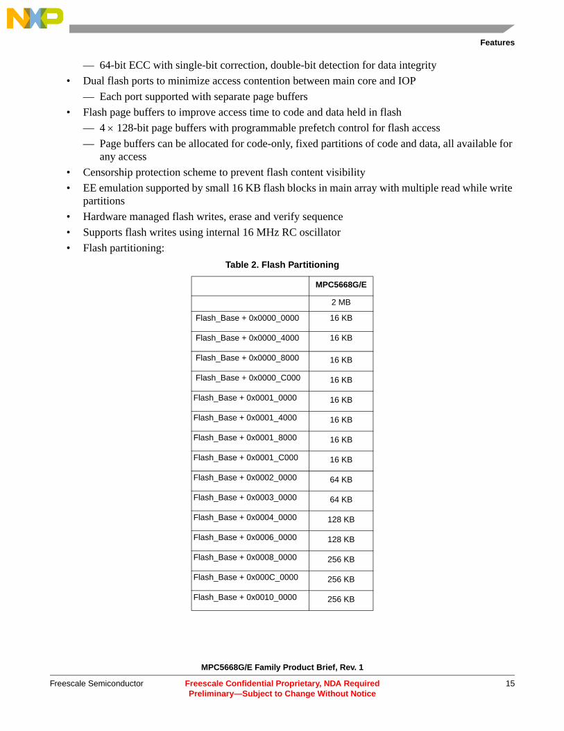
2.6.13 On-Chip Flash
On-chip flash on the MPC5668G/E features the following:• 2 MB burst flash memory
— Flash partitioning: 4 × 16 K; 4 × 16 K; 2 × 64 K; 2 × 128 K; 6 × 256 K— 16 KB shadow flash blocks— Typical flash access time: 0 wait-state for buffer hits, 3 wait-states for page buffer miss at
128 MHz
MPC5668G/E Family Product Brief, Rev. 1
Freescale Confidential Proprietary, NDA RequiredPreliminary—Subject to Change Without Notice
Freescale Semiconductor14
Features
— 64-bit ECC with single-bit correction, double-bit detection for data integrity• Dual flash ports to minimize access contention between main core and IOP
— Each port supported with separate page buffers• Flash page buffers to improve access time to code and data held in flash
— 4 × 128-bit page buffers with programmable prefetch control for flash access— Page buffers can be allocated for code-only, fixed partitions of code and data, all available for
any access• Censorship protection scheme to prevent flash content visibility• EE emulation supported by small 16 KB flash blocks in main array with multiple read while write
partitions• Hardware managed flash writes, erase and verify sequence• Supports flash writes using internal 16 MHz RC oscillator• Flash partitioning:
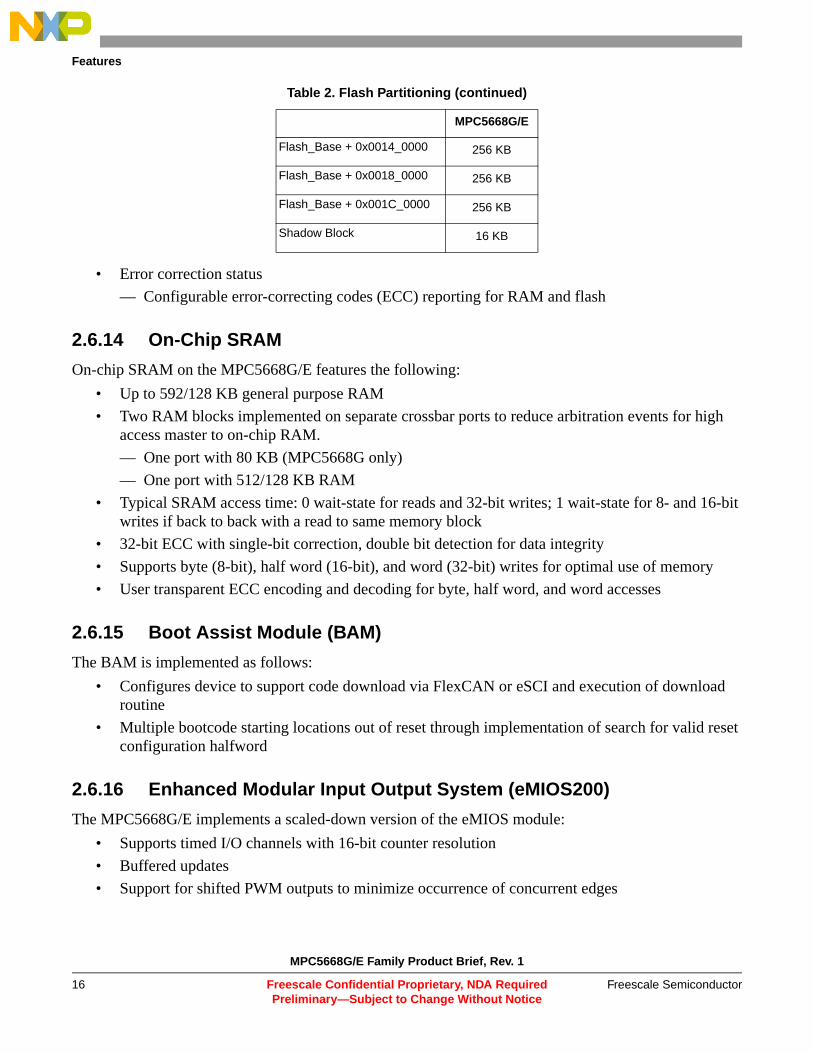
Table 2. Flash Partitioning
MPC5668G/E
2 MB
Flash_Base + 0x0000_0000 16 KB
Flash_Base + 0x0000_4000 16 KB
Flash_Base + 0x0000_8000 16 KB
Flash_Base + 0x0000_C000 16 KB
Flash_Base + 0x0001_0000 16 KB
Flash_Base + 0x0001_4000 16 KB
Flash_Base + 0x0001_8000 16 KB
Flash_Base + 0x0001_C000 16 KB
Flash_Base + 0x0002_0000 64 KB
Flash_Base + 0x0003_0000 64 KB
Flash_Base + 0x0004_0000 128 KB
Flash_Base + 0x0006_0000 128 KB
Flash_Base + 0x0008_0000 256 KB
Flash_Base + 0x000C_0000 256 KB
Flash_Base + 0x0010_0000 256 KB
MPC5668G/E Family Product Brief, Rev. 1
Freescale Confidential Proprietary, NDA RequiredPreliminary—Subject to Change Without Notice
Freescale Semiconductor 15
Features
• Error correction status— Configurable error-correcting codes (ECC) reporting for RAM and flash
2.6.14 On-Chip SRAM
On-chip SRAM on the MPC5668G/E features the following:• Up to 592/128 KB general purpose RAM• Two RAM blocks implemented on separate crossbar ports to reduce arbitration events for high
access master to on-chip RAM.— One port with 80 KB (MPC5668G only)— One port with 512/128 KB RAM
• Typical SRAM access time: 0 wait-state for reads and 32-bit writes; 1 wait-state for 8- and 16-bit writes if back to back with a read to same memory block
• 32-bit ECC with single-bit correction, double bit detection for data integrity• Supports byte (8-bit), half word (16-bit), and word (32-bit) writes for optimal use of memory• User transparent ECC encoding and decoding for byte, half word, and word accesses
2.6.15 Boot Assist Module (BAM)
The BAM is implemented as follows:• Configures device to support code download via FlexCAN or eSCI and execution of download
routine• Multiple bootcode starting locations out of reset through implementation of search for valid reset
configuration halfword
2.6.16 Enhanced Modular Input Output System (eMIOS200)
The MPC5668G/E implements a scaled-down version of the eMIOS module:• Supports timed I/O channels with 16-bit counter resolution• Buffered updates• Support for shifted PWM outputs to minimize occurrence of concurrent edges
Flash_Base + 0x0014_0000 256 KB
Flash_Base + 0x0018_0000 256 KB
Flash_Base + 0x001C_0000 256 KB
Shadow Block 16 KB
Table 2. Flash Partitioning (continued)
MPC5668G/E
MPC5668G/E Family Product Brief, Rev. 1
Freescale Confidential Proprietary, NDA RequiredPreliminary—Subject to Change Without Notice
Freescale Semiconductor16
Features
• Supports configurable trigger outputs for ADC conversions for synchronization to channel output waveforms
• Edge aligned output pulse width modulation— Programmable pulse period and duty cycle— Supports 0% and 100% duty cycle— Shared or independent time bases
• Up to 32 1 single action channels offering input capture and output compare functions• Up to 32 1 dual action channels offering output pulse width modulation, • Up to 13 1 output pulse width and frequency modulation and center aligned output PWM channels
with dead time.• Up to 5 1 modulus up/down counters that can be used to drive counter buses. • DMA transfer support available
2.6.17 Analog to Digital Converter Module (ADC)
The MPC5668G/E ADC features the following:• 10-bit A/D resolution• 0–VDD common mode conversion range• Supports conversions speeds of up to 1 µs• Internally multiplexed channels
— 10-bit ± 2 counts accuracy (TUE) available for 16 channels— 10-bit ± 3 counts accuracy (TUE) available for remaining channels— Dedicated result register available for every internally muxed channel
• Externally multiplexed channels — Internal control to support generation of external analog multiplexor selection— Four internal channels optionally used to support externally multiplex inputs, providing
transparent control for additional ADC channels— Each of the four channels supports up to 8 externally muxed inputs
• Three independently configurable sample and conversion times for high occurrence channels, internally muxed channels and externally muxed channels
• Right-aligned result format• Support for one-shot, scan and injection conversion modes• Traceability of each channels with conversion result. • Injection mode status bit implemented on adjacent 16-bit register for each result• Independently configurable parameters for channels:
— Offset refresh— Sampling
1. Depends on pin muxing and product derivative
MPC5668G/E Family Product Brief, Rev. 1
Freescale Confidential Proprietary, NDA RequiredPreliminary—Subject to Change Without Notice
Freescale Semiconductor 17
Features
• Cross Triggering support (MPC5668E only)— Internal conversion triggering from periodic interrupt timer (PIT) or timed I/O module
(eMIOS200) via Cross Triggering Unit (CTU)— One input pin configurable as external conversion trigger source
• Four configurable analog comparator channels offering range comparison with triggered alarm • Supports operation of ADC using internal 16 MHz RC oscillator• All unused analog pins available as general purpose input pins• Selected unused analog pins available as general purpose output pins• Power-down mode• Supports for DMA transfer of results
2.6.18 Cross Triggering Unit (CTU)
The CTU features the following:• Collection of 9 bit timers with an exponential prescaler able to generate the trigger event for ADC
conversions• 9-bit down counters counting from a programmable start value to 0• Different counters associated with different channel groups• Channel group is defined based on PWM channel clock• Different delay value for each eMIOS flag/PIT event• 4-bit programmable exponential prescaler• Single cycle delayed trigger output. Trigger output is a combination of 64 input flags/events
connected to different timers in the system• Maskable interrupt generation whenever a trigger output is generated• Event configuration registers dedicated to UC flag/triggering event• Acknowledgement signal to eMIOS for clearing the flag• Synchronization with ADC to avoid collision
2.6.19 Deserial Serial Peripheral Interface Module (DSPI)
The MPC5668G/E DSPI features the following:• Full duplex, synchronous transfers• Master or slave operation• Programmable master bit rates• Programmable clock polarity and phase• End-of-transmission interrupt flag• Programmable transfer baud rate• Programmable data frames from 4 to 16 bits
MPC5668G/E Family Product Brief, Rev. 1
Freescale Confidential Proprietary, NDA RequiredPreliminary—Subject to Change Without Notice
Freescale Semiconductor18
Features
• Up to 24 chip select lines available (6 per DSPI module); the number available at any time is dependent on package and pin multiplexing.
• Up to 4 independently configurable transfer types can be configured for each DSPI using the clock and transfer attributes registers
• Chip select strobe available as alternate function on one of the chip select pins for de-glitching• FIFOs for buffering up to 4 transfers on the transmit and receive side• General purpose I/O functionality on pins when not used for DSPI• Queueing operation possible through use of eDMA• Serialization of selected sources (eMIOS channels and Phantom ports in SIU)
2.6.20 Serial Communication Interface Module (eSCI)
The eSCI on the MPC5668G/E features the following:• Full-duplex operation• Standard mark/space non-return-to-zero (NRZ) format• 13-bit baud rate selection• Programmable 8-bit or 9-bit data format• LIN master node automation support• Separately enabled transmitter and receiver• Two receiver wakeup methods:
— Idle line wakeup— Address mark wakeup
• Interrupt driven with flags• Receiver framing error detection• Hardware parity checking• 1/16 bit-time noise detection• Two channel DMA interface
2.6.21 Controller Area Network Module (FlexCAN)
The enhanced FlexCAN module features the following:• Compliant with CAN protocol specification, Version 2.0B active• 64 mailboxes, each configurable as transmit or receive
— Mailboxes configurable while module remains syncronised to CAN bus• Transmit features
— Arbitration scheme according to message ID, message buffer number or local priority— Internal arbitration to guarantee no inner priority inversion— Multiple transmit buffers to avoid outer priority inversion— Transmit abort procedure and notification
MPC5668G/E Family Product Brief, Rev. 1
Freescale Confidential Proprietary, NDA RequiredPreliminary—Subject to Change Without Notice
Freescale Semiconductor 19
Features
• Receive features— Individual programmable filters for each mailbox— Hardware FIFO can be enabled
– 8 mailboxes can be configured to provide a 6-entry receive FIFO and 8 programmable acceptance filters
• Programmable clock source— System clock— Direct oscillator clock to avoid PLL jitter— Listen only mode capabilities
2.6.22 Inter IC Communications Module (I2C)
The I2C module features the following:• Two-wire bi-directional serial bus for on-board communications• Compatibility with I2C bus standard• Multimaster operation• Software-programmable for one of 256 different serial clock frequencies• Software-selectable acknowledge bit• Interrupt-driven, byte-by-byte data transfer• Arbitration-lost interrupt with automatic mode switching from master to slave• Calling address identification interrupt• Start and stop signal generation/detection• Repeated START signal generation• Acknowledge bit generation/detection• Bus-busy detection
2.6.23 Dual-Channel FlexRay Controller (FR)
The dual-channel FlexRay controller features the following:• Full implementation of FlexRay Protocol Specification 2.1, RevA• Single channel support
— FlexRay PortA can be configured to be connected either to physical FlexRay channel A or physical FlexRay channel B
• FlexRay bus data rates of 10, 8, 5, and 2.5 Mbit/s supported• Up to 128 configurable message buffers with
— Individual frame ID filtering— Individual channel ID filtering— Individual cycle counter filtering
• Message buffer header, status and payload data stored in dedicated FlexRay memory
MPC5668G/E Family Product Brief, Rev. 1
Freescale Confidential Proprietary, NDA RequiredPreliminary—Subject to Change Without Notice
Freescale Semiconductor20
Features
— Allows for flexible and efficient message buffer implementation— Consistent data access ensured by means of buffer locking scheme— Application can lock multiple buffers at the same time
• Message buffers can be configured as:— Receive message buffer— Single buffered transmit message buffer— Double buffered transmit message buffer (combines two single buffered message buffers)
• Individual message buffer reconfiguration supported• Two independent receive FIFOs
— One receive FIFO per channel— Up to 255 entries for each FIFO— Global frame ID filtering, based on both value/mask filters and range filters— Global channel ID filtering— Global message ID filtering for dynamic segment
• Size of message buffer payload data configurable from 0 up to 254 bytes• Two independent message buffer segments with configurable size of payload data section
– Each segment can contain message buffers assigned to the static segment and message buffers assigned to the dynamic segment at the same time
• Support for independent internal clock source provided to module from a separate external 40 MHz crystal
• 1 absolute timer— 1 timer that can be configured to absolute or relative
2.6.24 Periodic Interrupt Timer Module (PIT)
The PIT features the following:• Up to 8 general purpose interrupt timers• Up to 2 interrupt timers for triggering ADC conversions• 32-bit counter resolution• Clocked by system clock frequency
2.6.25 System Timer Module (STM)
One STM supporting • One 32-bit up counter with 8-bit prescaler • Four 32-bit compare channels running off the same up-counter • Independent interrupt source for each channel • Clocked by the main system clock • Instantiated in the same CPU clock domain
MPC5668G/E Family Product Brief, Rev. 1
Freescale Confidential Proprietary, NDA RequiredPreliminary—Subject to Change Without Notice
Freescale Semiconductor 21
Features
• Counter can be stopped in debug mode
2.6.26 Real Time Counter (RTC)
Real Time counter supports wake-up from Low Power modes or real time clock generation• Configurable resolution for different timeout periods
— 1 sec resolution for > 1 hour period— 1 ms resolution for 2-second period
• Selectable clock sources from:— Internal 128 KHz RC oscillator— Internal 16 MHz RC oscillator— 32 KHz external oscillator
• RTC supports continued operation through reset, count only reset manually, or by power on reset (POR)
2.6.27 JTAG controller (JTAGC)
The JTAGC is compliant with the IEEE 1149.1-2001standard and has the following main features:• IEEE 1149.1-2001 test access port (TAP) interface• A JCOMP input that provides the ability to share the TAP• A 5-bit instruction register that supports several IEEE 1149.1-2001 defined instructions, as well as
several public and private MCU specific instructions• Three test data registers: Bypass register, boundary scan register and a device identification register• Supporting boundary scan testing• TAP controller state machine
2.6.28 Nexus Development Interface (NDI)
The NDI module is compliant with the IEEE-ISTO 5001-2003 standard. The following features are implemented, but only available on the 256 MAPBGA emulation package:
• 17-bit full duplex pin interface for medium and high visibility throughput— Full port mode (12 MDO)— Auxiliary input port (MCKO, 12xMDO, 2xMSEO, EVTO, EVTI)— Auxiliary output port— 5 pin JTAG port (JCOMP, TDI, TDO, TMS and TCK)
The NPC block performs the following functions• Controls arbitration between e200Z6 and e200Z0 Nexus modules to the Nexus Auxiliary output
port• Generates full port mode indication output port• Generates MCKO and frequency division (1/2, 1/4, 1/8).
MPC5668G/E Family Product Brief, Rev. 1
Freescale Confidential Proprietary, NDA RequiredPreliminary—Subject to Change Without Notice
Freescale Semiconductor22
Developer Environment
• Controls sharing of EVTO/EVTI• Enables gating of MCKO when the auxiliary output port is idle.
e200Z6 development support features (Nexus class3)• IEEE-ISTO 5001-2003 standard class 3 compliant• Program trace via branch trace messaging (BTM)• Data trace via data write messaging (DWM) and data read messaging (DRM). This allows the
development tools to trace reads and /or writes to selected internal memory resources• Ownership via ownership trace messaging (OTM). OTM facilitates ownership trace by providing
visibility of which process ID or operating system task is activated• Run-time access to the e200Z6 memory map via the JTAG port• Watchpoint messaging • Watchpoint trigger enable of program and/or data trace messaging
e200Z0 development support features (Nexus class 2+)• IEEE-ISTO 5001-2003 standard class 2 compliant with additional class 3 and 4 features available• Program trace via branch trace messaging (BTM)• Ownership via ownership trace messaging (OTM)
— OTM facilitates ownership trace by providing visibility of which process ID or operating system task is activated
• Run-time access to the e200Z6 memory map via the JTAG port• Watchpoint messaging • Watchpoint trigger enable of program and/or data trace messaging
Capability of an event output signal from either core to generate a debug request in the other core• All Nexus port pins operate at 3.3 V levels• Nexus supports debug through reset and low power
3 Developer EnvironmentThe MPC5668G/E family of MCUs supports similar tools and third party developers as other Freescale MPC5500 and MPC5510 products, offering a widespread, established network of tools and software vendors. It also features a high-performance Nexus debug interface.
The following development support will be available:• Automotive evaluation boards (EVB) featuring CAN, LIN interfaces, and more• Compilers• Debuggers• JTAG and Nexus interfaces
The following software support will be available:• Optimized AutoSAR OS supported
MPC5668G/E Family Product Brief, Rev. 1
Freescale Confidential Proprietary, NDA RequiredPreliminary—Subject to Change Without Notice
Freescale Semiconductor 23
Developer Environment
• AutoSAR MCAL layer• Flash and EEPROM drivers• FlexRay, CAN and LIN drivers from 3rd parties
MPC5668G/E Family Product Brief, Rev. 1
Freescale Confidential Proprietary, NDA RequiredPreliminary—Subject to Change Without Notice
Freescale Semiconductor24
Document Number: MPC5668xPBRev. 103/2008
How to Reach Us:
Home Page:www.freescale.com
Web Support:http://www.freescale.com/support
USA/Europe or Locations Not Listed:Freescale SemiconductorTechnical Information Center, EL5162100 East Elliot RoadTempe, Arizona 85284+1-800-521-6274 or +1-480-768-2130www.freescale.com/support
Europe, Middle East, and Africa:Freescale Halbleiter Deutschland GmbHTechnical Information CenterSchatzbogen 781829 Muenchen, Germany+44 1296 380 456 (English)+46 8 52200080 (English)+49 89 92103 559 (German)+33 1 69 35 48 48 (French)www.freescale.com/support
Japan:Freescale Semiconductor Japan Ltd.HeadquartersARCO Tower 15F1-8-1, Shimo-Meguro, Meguro-ku,Tokyo 153-0064Japan0120 191014 or +81 3 5437 [email protected]
Asia/Pacific:Freescale Semiconductor Hong Kong Ltd.Technical Information Center2 Dai King StreetTai Po Industrial EstateTai Po, N.T., Hong Kong+800 2666 [email protected]
For Literature Requests Only:Freescale Semiconductor Literature Distribution CenterP.O. Box 5405Denver, Colorado 802171-800-441-2447 or 303-675-2140Fax: [email protected]
Information in this document is provided solely to enable system and software implementers to use Freescale Semiconductor products. There are no express or implied copyright licenses granted hereunder to design or fabricate any integrated circuits or integrated circuits based on the information in this document.
Freescale Semiconductor reserves the right to make changes without further notice to any products herein. Freescale Semiconductor makes no warranty, representation or guarantee regarding the suitability of its products for any particular purpose, nor does Freescale Semiconductor assume any liability arising out of the application or use of any product or circuit, and specifically disclaims any and all liability, including without limitation consequential or incidental damages. “Typical” parameters that may be provided in Freescale Semiconductor data sheets and/or specifications can and do vary in different applications and actual performance may vary over time. All operating parameters, including “Typicals”, must be validated for each customer application by customer’s technical experts. Freescale Semiconductor does not convey any license under its patent rights nor the rights of others. Freescale Semiconductor products are not designed, intended, or authorized for use as components in systems intended for surgical implant into the body, or other applications intended to support or sustain life, or for any other application in which the failure of the Freescale Semiconductor product could create a situation where personal injury or death may occur. Should Buyer purchase or use Freescale Semiconductor products for any such unintended or unauthorized application, Buyer shall indemnify and hold Freescale Semiconductor and its officers, employees, subsidiaries, affiliates, and distributors harmless against all claims, costs, damages, and expenses, and reasonable attorney fees arising out of, directly or indirectly, any claim of personal injury or death associated with such unintended or unauthorized use, even if such claim alleges that Freescale Semiconductor was negligent regarding the design or manufacture of the part.
Freescale™ and the Freescale logo are trademarks of Freescale Semiconductor, Inc. All other product or service names are the property of their respective owners.The Power Architecture and Power.org word marks and the Power and Power.org logos and related marks are trademarks and service marks licensed by Power.org.
© Freescale Semiconductor, Inc. 2008. All rights reserved.
Freescale Confidential Proprietary, NDA RequiredPreliminary—Subject to Change Without Notice