Embed Size (px)
Citation preview
32SH7616
Hardware Manual
Renesas 32-Bit RISC MicrocomputerSuperH� RISC engine Family/SH7600 Series
SH7616 HD6417616
REJ09B0292-0200
Revision Date: Mar 09, 2006Rev. 2.00

Rev. 2.00 Mar 09, 2006 page ii of xxvi
1. These materials are intended as a reference to assist our customers in the selection of the Renesas Technology Corp. product best suited to the customer's application; they do not convey any license under any intellectual property rights, or any other rights, belonging to Renesas Technology Corp. or a third party.
2. Renesas Technology Corp. assumes no responsibility for any damage, or infringement of any third-party's rights, originating in the use of any product data, diagrams, charts, programs, algorithms, or circuit application examples contained in these materials.
3. All information contained in these materials, including product data, diagrams, charts, programs and algorithms represents information on products at the time of publication of these materials, and are subject to change by Renesas Technology Corp. without notice due to product improvements or other reasons. It is therefore recommended that customers contact Renesas Technology Corp. or an authorized Renesas Technology Corp. product distributor for the latest product information before purchasing a product listed herein. The information described here may contain technical inaccuracies or typographical errors. Renesas Technology Corp. assumes no responsibility for any damage, liability, or other loss rising from these inaccuracies or errors. Please also pay attention to information published by Renesas Technology Corp. by various means, including the Renesas Technology Corp. Semiconductor home page (http://www.renesas.com).
4. When using any or all of the information contained in these materials, including product data, diagrams, charts, programs, and algorithms, please be sure to evaluate all information as a total system before making a final decision on the applicability of the information and products. Renesas Technology Corp. assumes no responsibility for any damage, liability or other loss resulting from the information contained herein.
5. Renesas Technology Corp. semiconductors are not designed or manufactured for use in a device or system that is used under circumstances in which human life is potentially at stake. Please contact Renesas Technology Corp. or an authorized Renesas Technology Corp. product distributor when considering the use of a product contained herein for any specific purposes, such as apparatus or systems for transportation, vehicular, medical, aerospace, nuclear, or undersea repeater use.
6. The prior written approval of Renesas Technology Corp. is necessary to reprint or reproduce in whole or in part these materials.
7. If these products or technologies are subject to the Japanese export control restrictions, they must be exported under a license from the Japanese government and cannot be imported into a country other than the approved destination. Any diversion or reexport contrary to the export control laws and regulations of Japan and/or the country of destination is prohibited.
8. Please contact Renesas Technology Corp. for further details on these materials or the products contained therein.
1. Renesas Technology Corp. puts the maximum effort into making semiconductor products better and more reliable, but there is always the possibility that trouble may occur with them. Trouble with semiconductors may lead to personal injury, fire or property damage. Remember to give due consideration to safety when making your circuit designs, with appropriate measures such as (i) placement of substitutive, auxiliary circuits, (ii) use of nonflammable material or (iii) prevention against any malfunction or mishap.
Keep safety first in your circuit designs!
Notes regarding these materials
Rev. 2.00 Mar 09, 2006 page iii of xxvi
Preface
The SH7616 is a microprocessor that integrates peripheral functions necessary for systemconfiguration with a 32-bit internal architecture SH2-DSP CPU as its core.
The SH7616's on-chip peripheral functions include a cache memory, an interrupt controller,timers, an ethernet controller (EtherC), DSP, a serial communication interface with FIFO (SCIF),a USB function module, a user break controller (UBC), a bus state controller (BSC), a directmemory access cntroller (DMAC), and I/O ports, making it ideal for use as a microcomputer inelectronic devices that require high speed together with low power consumption.
Intended Readership: This manual is intended for users undertaking the design of an applicationsystem using the SH7616. Readers using this manual require a basicknowledge of electrical circuits, logic circuits, and microcomputers.
Purpose: The purpose of this manual is to give users an understanding of the hardwarefunctions and electrical characteristics of the SH7616. Details of executioninstructions can be found in the SH-1, SH-2, SH-DSP Programming Manual,which should be read in conjunction with the present manual.
Using this Manual:
• For an overall understanding of the SH7616's functionsFollow the Table of Contents. This manual is broadly divided into sections on the CPU, systemcontrol functions, peripheral functions, and electrical characteristics.
• For a detailed understanding of CPU functionsRefer to the separate publication SH-1, SH-2, SH-DSP Programming Manual.Note on bit notation: Bits are shown in high-to-low order from left to right.
Related Material: The latest information is available at our Web Site. Please make sure that youhave the most up-to-date information available.http://www.renesas.com/
Rev. 2.00 Mar 09, 2006 page iv of xxvi
User's Manuals on the SH7616:
Manual Title ADE No.
SH7616 Hardware Manual This manual
SH-1/ SH-2/SH-DSP Software Manual REJ09B0171-0500O
Users manuals for development tools:
Manual Title ADE No.
C/C++ Complier, Assembler, Optimized Linkage Editor User's Manual REJ10B0152-0101
Simulator Debugger Users Manual REJ10B0210-0200
High-performance Embedded Workshop Users Manual REJ10J0886-0300
Application Note:
Manual Title ADE No.
C/C++ Complier REJ05B0463-0300
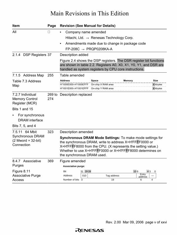
Main Revisions in This Edition
Item Page Revision (See Manual for Details)
All • Company name amendedHitachi, Ltd. → Renesas Technology Corp.
• Amendments made due to change in package codeFP-208C → PRQP0208KA-A
2.1.4 DSP Registers 37 Description added
Figure 2.4 shows the DSP registers. The DSR register bit functionsare shown in table 2.2. Registers A0, X0, X1, Y0, Y1, and DSR arehandled as system registers by CPU core instructions.
7.1.5 Address Map
Table 7.3 AddressMap
255 Table amendedAddress Space Memory Size
H'1000E000–H'1000EFFF On-chip X RAM area 4 kbytes
H'1001E000–H'1001EFFF On-chip Y RAM area 4 kbytes
7.2.7 IndividualMemory ControlRegister (MCR)
Bits 1 and 15
• For synchronousDRAM interface
Bits 7, 5, and 4
269 to274
Description replaced
7.5.11 64 MbitSynchronous DRAM(2 Mword × 32-bit)Connection
323 Description amended
Synchronous DRAM Mode Settings: To make mode settings forthe synchronous DRAM, write to address X+H'FFFF0000 orX+H'FFFF8000 from the CPU. (X represents the setting value.)Whether to use X+H'FFFF0000 or X+H'FFFF8000 determines onthe synchronous DRAM used.
8.4.7 AssociativePurges
Figure 8.11Associative PurgeAccess
369 Figure amended
Tag address010 Entryaddress —
31 10 9 4 3 0
19 63 4
29 28
Associative purge:
Address
Bit
Number of bits
Rev. 2.00 Mar 09, 2006 page v of xxvi
Item Page Revision (See Manual for Details)
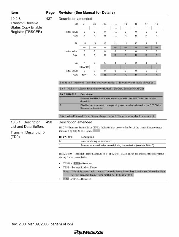
10.2.8 Transmit/ReceiveStatus Copy EnableRegister (TRSCER)
437 Description amendedBit: 31 30 29 . . .
. . .
19 18 17 16
— — — — — — —
Initial value: 0 0 0 . . .
. . .
0 0 0 0
R/W: R R R R R R R
Bit: 15 14 13 12 11 10 9 8
— — — — — — — —
Initial value: 0 0 0 0 0 0 0 0
R/W: R R R R R R R R
Bit: 7 6 5 4 3 2 1 0
RMAFCE — — — — — — —
Initial value: 0 0 0 0 0 0 0 0
R/W: R/W R R R R R R R
Bits 31 to 8—Reserved These bits are always read as 0. The write value should always be 0.
Bit 7—Multicast Address Frame Receive (RMAF): Bit Copy Enable (RMAFCE)
Bit 7: RMAFCE Description
0 Enables the RMAF bit status to be indicated in the RFS7 bit in the receive
descriptor.
1 Disables occurrence of corresponding source to be indicated in the RFS7 bit in
the receive descriptor.
Bits 6 to 0—Reserved: These bits are always read as 0. The write value should always be 0.
10.3.1 DescriptorList and Data Buffers
Transmit Descriptor 0(TD0)
450 Description amended
TFS9
en
Bit 27—Transmit Frame Error (TFE): Indicates that one or other bit of the transmit frame statusindicated by bits 26 to 0 is set.
Bit 27: TFE Description
0 No error during transmission
1 An error of some kind occurred during transmission (see bits 26 to 0)
Bits 26 to 0—Transmit Frame Status 26 to 0 (TFS26 to TFS0): These bits indicate the error statusduring frame transmission.
• TFS26 to —Reserved
• TFS8—Teransmit Abort Detect
Note: This bit is set to 1 wh any of Transmit Frame Status bits 4 to 0 is set. When this bit isset, the Transmit Frame Error bit (bit 27: TFE) is set to 1.
• TFS7 to TFS5—Reserved
Rev. 2.00 Mar 09, 2006 page vi of xxvi
Item Page Revision (See Manual for Details)
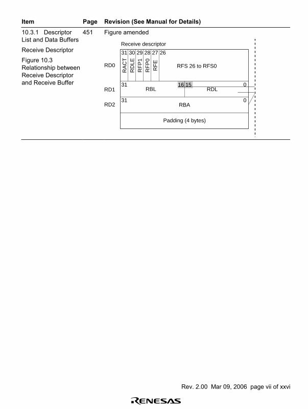
10.3.1 DescriptorList and Data Buffers
Receive Descriptor
Figure 10.3Relationship betweenReceive Descriptorand Receive Buffer
451 Figure amended
Receive descriptor
RA
CT
RD
LER
FP
1R
FP
0R
FE
RFS 26 to RFS0RD0
RBL RDL0
0
31
31 30 29 28 2627
31
RD1
RBA
Padding (4 bytes)
RD2
16 15
Rev. 2.00 Mar 09, 2006 page vii of xxvi
Item Page Revision (See Manual for Details)
Description amended
Bit 27�Receive Frame Error (RFE): Indicates that one or other bit ofthe receive frame status indicated by bits 26 to 0 is set. Whether ornot the multicast address frame receive information which is part ofthe frame status, is copied into this bit is specified by thetransmit/receive status copy enable register.
Bit 27: RFE Description0 No error during reception (Initial value)
1 An error of some kind occurred during reception (see bits26 to 0)
10.3.1 DescriptorList and Data Buffers
Receive Descriptor 0(TD0)
453
• Bits 26 to 0�Receive Frame Status 26 to 0 (RFS26 to RFS0):These bits indicate the error status during frame reception.
• RFS26 to RFS10�Reserved
• RFS9�Receive FIFO Overflow (corresponds to RFOF bit inEESR)
• RFS8�Reserve Abort DetectNote: This bit is set to 1 when any of Receive Frame Status
bit 9, bit 7, bits 4 to 0 is set. When this bit is set, theReceive Frame Error bit (bit 27: RFE) is set to 1.
• RFS7� Receive Multicast Address Frame (corresponds toRMAF bit in EESR)
• RFS6�Reserved*1
• RSF5� Receive Frame Discard Request Assertion(corresponds to RFAR bit in EESR)*1
• RFS4�Receive Residual-Bit Frame (corresponds to RRF bit inEESR)
• RFS3�Receive Too-Long Frame (corresponds to RTLF bit inEESR)
• RFS2�Receive Too-Short Frame (corresponds to RTSF bit inEESR)
• RFS1�PHY-LSI Receive Error (corresponds to PRE bit inEESR)
• RFS0�CRC Error on Received Frame (corresponds to CERF bitin EESR)Note: 1. Only HD6417616 is effective. HD6417615 is Reserved
Rev. 2.00 Mar 09, 2006 page viii of xxvi
bit.
Item Page Revision (See Manual for Details)
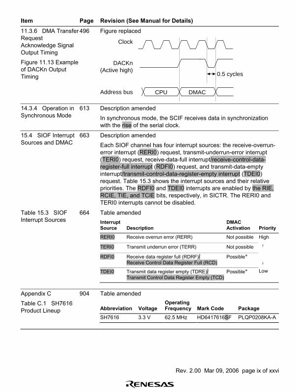
11.3.6 DMA TransferRequestAcknowledge SignalOutput Timing
Figure 11.13 Exampleof DACKn OutputTiming
496 Figure replaced
Clock
DACKn(Active high)
Address bus CPU DMAC
0.5 cycles
14.3.4 Operation inSynchronous Mode
613 Description amended
In synchronous mode, the SCIF receives data in synchronizationwith the rise of the serial clock.
15.4 SIOF InterruptSources and DMAC
663 Description amended
Each SIOF channel has four interrupt sources: the receive-overrun-error interrupt (RERI0) request, transmit-underrun-error interrupt(TERI0) request, receive-data-full interrupt/receive-control-data-register-full interrupt (RDFI0) request, and transmit-data-emptyinterrupt/transmit-control-data-register-empty interrupt (TDEI0)request. Table 15.3 shows the interrupt sources and their relativepriorities. The RDFI0 and TDEI0 interrupts are enabled by the RIE,RCIE, TIE, and TCIE bits, respectively, in SICTR. The RERI0 andTERI0 interrupts cannot be disabled.
Table amendedInterruptSource Description
DMACActivation Priority
RERI0 Receive overrun error (RERR) Not possible
TERI0 Transmit underrun error (TERR) Not possible
RDFI0 Receive data register full (RDRF)/Receive Control Data Register Full (RCD)
Possible*
TDEI0 Transmit data register empty (TDRE)/Transmit Control Data Register Empty (TCD)
Possible*
High
↑
↓
Low
Table 15.3 SIOFInterrupt Sources
664
Table amended
Abbreviation VoltageOperatingFrequency Mark Code Package
SH7616 3.3 V 62.5 MHz HD6417616SF PLQP0208KA-A
Appendix C
Table C.1 SH7616Product Lineup
904
Rev. 2.00 Mar 09, 2006 page ix of xxvi

Rev. 2.00 Mar 09, 2006 page x of xxvi
Rev. 2.00 Mar 09, 2006 page xi of xxvi
Contents
Section 1 Overview............................................................................................................. 11.1 Features of SuperH Microcomputer with On-Chip Ethernet Controller ........................... 11.2 Block Diagram .................................................................................................................. 131.3 Pin Description.................................................................................................................. 14
1.3.1 Pin Arrangement .................................................................................................. 141.3.2 Pin Functions ....................................................................................................... 151.3.3 Pin Multiplexing .................................................................................................. 21
1.4 Processing States............................................................................................................... 27
Section 2 CPU ...................................................................................................................... 312.1 Register Configuration ...................................................................................................... 31
2.1.1 General Registers ................................................................................................. 312.1.2 Control Registers ................................................................................................. 332.1.3 System Registers .................................................................................................. 362.1.4 DSP Registers ...................................................................................................... 372.1.5 Notes on Guard Bits and Overflow Treatment..................................................... 402.1.6 Initial Values of Registers.................................................................................... 40
2.2 Data Formats ..................................................................................................................... 412.2.1 Data Format in Registers...................................................................................... 412.2.2 Data Formats in Memory ..................................................................................... 412.2.3 Immediate Data Format ....................................................................................... 422.2.4 DSP Type Data Formats ...................................................................................... 422.2.5 DSP Type Instructions and Data Formats ............................................................ 44
2.3 CPU Core Instruction Features ......................................................................................... 482.4 Instruction Formats ........................................................................................................... 52
2.4.1 CPU Instruction Addressing Modes..................................................................... 522.4.2 DSP Data Addressing........................................................................................... 562.4.3 Instruction Formats for CPU Instructions ............................................................ 622.4.4 Instruction Formats for DSP Instructions............................................................. 66
2.5 Instruction Set ................................................................................................................... 722.5.1 CPU Instruction Set ............................................................................................. 732.5.2 DSP Data Transfer Instruction Set ....................................................................... 892.5.3 DSP Operation Instruction Set ............................................................................. 932.5.4 Various Operation Instructions ............................................................................ 96
2.6 Usage Notes ...................................................................................................................... 1052.6.1 When not using DSP instructions ........................................................................ 105
Rev. 2.00 Mar 09, 2006 page xii of xxvi
2.6.2 When executing a combination of double-precision multiplication ordouble-precision product-sum operation (CPU instruction) and DSPcomputing instruction .......................................................................................... 105
Section 3 Oscillator Circuits and Operating Modes .................................................. 1073.1 Overview........................................................................................................................... 1073.2 On-Chip Clock Pulse Generator and Operating Modes .................................................... 107
3.2.1 Clock Pulse Generator ......................................................................................... 1073.2.2 Clock Operating Mode Settings........................................................................... 1093.2.3 Connecting a Crystal Resonator........................................................................... 1123.2.4 External Clock Input ............................................................................................ 1133.2.5 Operating Frequency Selection by Register......................................................... 1143.2.6 Clock Modes and Frequency Ranges................................................................... 1223.2.7 Notes on Board Design ........................................................................................ 123
3.3 Bus Width of the CS0 Area............................................................................................... 124
Section 4 Exception Handling ......................................................................................... 1254.1 Overview........................................................................................................................... 125
4.1.1 Types of Exception Handling and Priority Order ................................................ 1254.1.2 Exception Handling Operations ........................................................................... 1274.1.3 Exception Vector Table ....................................................................................... 128
4.2 Resets ................................................................................................................................ 1314.2.1 Types of Resets .................................................................................................... 1314.2.2 Power-On Reset ................................................................................................... 1314.2.3 Manual Reset ....................................................................................................... 132
4.3 Address Errors .................................................................................................................. 1324.3.1 Sources of Address Errors ................................................................................... 1324.3.2 Address Error Exception Handling ...................................................................... 134
4.4 Interrupts ........................................................................................................................... 1354.4.1 Interrupt Sources.................................................................................................. 1354.4.2 Interrupt Priority Levels....................................................................................... 1364.4.3 Interrupt Exception Handling............................................................................... 136
4.5 Exceptions Triggered by Instructions ............................................................................... 1374.5.1 Instruction-Triggered Exception Types ............................................................... 1374.5.2 Trap Instructions .................................................................................................. 1374.5.3 Illegal Slot Instructions ........................................................................................ 1384.5.4 General Illegal Instructions.................................................................................. 138
4.6 When Exception Sources Are Not Accepted .................................................................... 1394.6.1 Immediately after a Delayed Branch Instruction ................................................. 1394.6.2 Immediately after an Interrupt-Disabled Instruction............................................ 139
Rev. 2.00 Mar 09, 2006 page xiii of xxvi
4.6.3 Instructions in Repeat Loops................................................................................ 1404.7 Stack Status after Exception Handling.............................................................................. 1414.8 Usage Notes ...................................................................................................................... 142
4.8.1 Value of Stack Pointer (SP) ................................................................................. 1424.8.2 Value of Vector Base Register (VBR) ................................................................. 1424.8.3 Address Errors Caused by Stacking of Address Error Exception Handling ........ 1424.8.4 Manual Reset during Register Access.................................................................. 142
Section 5 Interrupt Controller (INTC)........................................................................... 1435.1 Overview........................................................................................................................... 143
5.1.1 Features ................................................................................................................ 1435.1.2 Block Diagram..................................................................................................... 1435.1.3 Pin Configuration................................................................................................. 1455.1.4 Register Configuration......................................................................................... 145
5.2 Interrupt Sources ............................................................................................................... 1465.2.1 NMI Interrupt....................................................................................................... 1475.2.2 User Break Interrupt............................................................................................. 1475.2.3 H-UDI Interrupt ................................................................................................... 1475.2.4 IRL Interrupts....................................................................................................... 1475.2.5 IRQ Interrupts ...................................................................................................... 1485.2.6 On-chip Peripheral Module Interrupts ................................................................. 1525.2.7 Interrupt Exception Vectors and Priority Order ................................................... 152
5.3 Register Descriptions ........................................................................................................ 1595.3.1 Interrupt Priority Level Setting Register A (IPRA) ............................................. 1595.3.2 Interrupt Priority Level Setting Register B (IPRB).............................................. 1605.3.3 Interrupt Priority Level Setting Register C (IPRC).............................................. 1615.3.4 Interrupt Priority Level Setting Register D (IPRD) ............................................. 1625.3.5 Interrupt Priority Level Setting Register E (IPRE) .............................................. 1635.3.6 Vector Number Setting Register WDT (VCRWDT) ........................................... 1645.3.7 Vector Number Setting Register A (VCRA)........................................................ 1655.3.8 Vector Number Setting Register B (VCRB) ........................................................ 1665.3.9 Vector Number Setting Register C (VCRC) ........................................................ 1665.3.10 Vector Number Setting Register D (VCRD)........................................................ 1675.3.11 Vector Number Setting Register E (VCRE) ........................................................ 1685.3.12 Vector Number Setting Register F (VCRF)......................................................... 1695.3.13 Vector Number Setting Register G (VCRG)........................................................ 1705.3.14 Vector Number Setting Register H (VCRH)........................................................ 1715.3.15 Vector Number Setting Register I (VCRI)........................................................... 1725.3.16 Vector Number Setting Register J (VCRJ) .......................................................... 1735.3.17 Vector Number Setting Register K (VCRK)........................................................ 174
Rev. 2.00 Mar 09, 2006 page xiv of xxvi
5.3.18 Vector Number Setting Register L (VCRL) ........................................................ 1755.3.19 Vector Number Setting Register M (VCRM) ...................................................... 1765.3.20 Vector Number Setting Register N (VCRN)........................................................ 1775.3.21 Vector Number Setting Register O (VCRO)........................................................ 1785.3.22 Vector Number Setting Register P (VCRP)......................................................... 1795.3.23 Vector Number Setting Register Q (VCRQ)........................................................ 1805.3.24 Vector Number Setting Register R (VCRR) ........................................................ 1815.3.25 Vector Number Setting Register S (VCRS)......................................................... 1825.3.26 Vector Number Setting Register T (VCRT) ........................................................ 1835.3.27 Vector Number Setting Register U (VCRU)........................................................ 1845.3.28 Interrupt Control Register (ICR).......................................................................... 1875.3.29 IRQ Control/Status Register (IRQCSR) .............................................................. 188
5.4 Interrupt Operation............................................................................................................ 1905.4.1 Interrupt Sequence ............................................................................................... 1905.4.2 Stack State after Interrupt Exception Handling.................................................... 192
5.5 Interrupt Response Time................................................................................................... 1925.6 Sampling of Pins IRL3�IRL0 ........................................................................................... 1945.7 Usage Notes ...................................................................................................................... 195
Section 6 User Break Controller (UBC) ....................................................................... 1996.1 Overview........................................................................................................................... 199
6.1.1 Features................................................................................................................ 1996.1.2 Block Diagram..................................................................................................... 2006.1.3 Register Configuration......................................................................................... 201
6.2 Register Descriptions ........................................................................................................ 2036.2.1 Break Address Register A (BARA) ..................................................................... 2036.2.2 Break Address Mask Register A (BAMRA)........................................................ 2046.2.3 Break Bus Cycle Register A (BBRA).................................................................. 2056.2.4 Break Address Register B (BARB) ..................................................................... 2076.2.5 Break Address Mask Register B (BAMRB) ........................................................ 2086.2.6 Break Bus Cycle Register B (BBRB) .................................................................. 2096.2.7 Break Address Register C (BARC)...................................................................... 2116.2.8 Break Address Mask Register C (BAMRC) ........................................................ 2126.2.9 Break Data Register C (BDRC) ........................................................................... 2146.2.10 Break Data Mask Register C (BDMRC).............................................................. 2156.2.11 Break Bus Cycle Register C (BBRC) .................................................................. 2176.2.12 Break Execution Times Register C (BETRC) ..................................................... 2186.2.13 Break Address Register D (BARD) ..................................................................... 2196.2.14 Break Address Mask Register D (BAMRD)........................................................ 2206.2.15 Break Data Register D (BDRD)........................................................................... 222
Rev. 2.00 Mar 09, 2006 page xv of xxvi
6.2.16 Break Data Mask Register D (BDMRD) ............................................................. 2236.2.17 Break Bus Cycle Register D (BBRD).................................................................. 2256.2.18 Break Execution Times Register D (BETRD) ..................................................... 2266.2.19 Break Control Register (BRCR) .......................................................................... 2276.2.20 Branch Flag Registers (BRFR) ............................................................................ 2336.2.21 Branch Source Registers (BRSR) ........................................................................ 2346.2.22 Branch Destination Registers (BRDR) ................................................................ 235
6.3 Operation........................................................................................................................... 2366.3.1 User Break Operation Sequence .......................................................................... 2366.3.2 Instruction Fetch Cycle Break.............................................................................. 2376.3.3 Data Access Cycle Break..................................................................................... 2386.3.4 Saved Program Counter (PC) Value .................................................................... 2396.3.5 X Memory Bus or Y Memory Bus Cycle Break .................................................. 2396.3.6 Sequential Break .................................................................................................. 2406.3.7 PC Traces............................................................................................................. 2416.3.8 Examples of Use .................................................................................................. 2436.3.9 Usage Notes ......................................................................................................... 247
Section 7 Bus State Controller (BSC) ........................................................................... 2497.1 Overview........................................................................................................................... 249
7.1.1 Features ................................................................................................................ 2497.1.2 Block Diagram..................................................................................................... 2517.1.3 Pin Configuration................................................................................................. 2527.1.4 Register Configuration......................................................................................... 2547.1.5 Address Map ........................................................................................................ 255
7.2 Register Descriptions ........................................................................................................ 2577.2.1 Bus Control Register 1 (BCR1) ........................................................................... 2577.2.2 Bus Control Register 2 (BCR2) ........................................................................... 2607.2.3 Bus Control Register 3 (BCR3) ........................................................................... 2617.2.4 Wait Control Register 1 (WCR1)......................................................................... 2637.2.5 Wait Control Register 2 (WCR2)......................................................................... 2657.2.6 Wait Control Register 3 (WCR3)......................................................................... 2677.2.7 Individual Memory Control Register (MCR)....................................................... 2687.2.8 Refresh Timer Control/Status Register (RTCSR) ................................................ 2767.2.9 Refresh Timer Counter (RTCNT)........................................................................ 2787.2.10 Refresh Time Constant Register (RTCOR) ......................................................... 278
7.3 Access Size and Data Alignment ...................................................................................... 2797.3.1 Connection to Ordinary Devices.......................................................................... 2797.3.2 Connection to Little-Endian Devices ................................................................... 280
7.4 Accessing Ordinary Space ................................................................................................ 282

Rev. 2.00 Mar 09, 2006 page xvi of xxvi
7.4.1 Basic Timing........................................................................................................ 2827.4.2 Wait State Control................................................................................................ 2877.4.3 CS Assertion Period Extension ............................................................................ 291
7.5 Synchronous DRAM Interface.......................................................................................... 2927.5.1 Synchronous DRAM Direct Connection ............................................................. 2927.5.2 Address Multiplexing........................................................................................... 2947.5.3 Burst Reads .......................................................................................................... 2967.5.4 Single Reads ........................................................................................................ 3017.5.5 Single Writes........................................................................................................ 3037.5.6 Burst Write Mode ................................................................................................ 3047.5.7 Bank Active Function .......................................................................................... 3067.5.8 Refreshes.............................................................................................................. 3177.5.9 Overlap Between Auto Precharge Cycle (Tap) and Next Access ........................ 3207.5.10 Power-On Sequence............................................................................................. 3217.5.11 64 Mbit Synchronous DRAM (2 Mword × 32-bit) Connection........................... 323
7.6 DRAM Interface ............................................................................................................... 3247.6.1 DRAM Direct Connection ................................................................................... 3247.6.2 Address Multiplexing........................................................................................... 3257.6.3 Basic Timing........................................................................................................ 3267.6.4 Wait State Control................................................................................................ 3277.6.5 Burst Access ........................................................................................................ 3297.6.6 EDO Mode........................................................................................................... 3327.6.7 DRAM Single Transfer........................................................................................ 3367.6.8 Refreshing............................................................................................................ 3377.6.9 Power-On Sequence............................................................................................. 339
7.7 Burst ROM Interface......................................................................................................... 3397.8 Idles between Cycles......................................................................................................... 3437.9 Bus Arbitration.................................................................................................................. 345
7.9.1 Master Mode ........................................................................................................ 3497.10 Additional Items................................................................................................................ 350
7.10.1 Resets................................................................................................................... 3507.10.2 Access as Viewed from CPU, DMAC or E-DMAC ............................................ 3517.10.3 STATS1 and STATS0 Pins ................................................................................. 3527.10.4 BUSHiZ Specification ......................................................................................... 353
7.11 Usage Notes ...................................................................................................................... 3547.11.1 Normal Space Access after Synchronous DRAM Write when Using DMAC..... 3547.11.2 When Using Iφ: Eφ Clock Ratio of 1: 1, 8-Bit Bus Width,
and External Wait Input ....................................................................................... 3567.11.3 When connecting external device to synchronous DRAM .................................. 356
Rev. 2.00 Mar 09, 2006 page xvii of xxvi
Section 8 Cache.................................................................................................................... 3578.1 Introduction....................................................................................................................... 357
8.1.1 Register Configuration......................................................................................... 3588.2 Register Description.......................................................................................................... 358
8.2.1 Cache Control Register (CCR)............................................................................. 3588.3 Address Space and the Cache............................................................................................ 3608.4 Cache Operation................................................................................................................ 361
8.4.1 Cache Reads......................................................................................................... 3618.4.2 Write Access ........................................................................................................ 3638.4.3 Cache-Through Access ........................................................................................ 3668.4.4 The TAS Instruction............................................................................................. 3668.4.5 Pseudo-LRU and Cache Replacement ................................................................. 3668.4.6 Cache Initialization .............................................................................................. 3688.4.7 Associative Purges ............................................................................................... 3688.4.8 Cache Flushing..................................................................................................... 3698.4.9 Data Array Access ............................................................................................... 3698.4.10 Address Array Access.......................................................................................... 370
8.5 Cache Use ......................................................................................................................... 3718.5.1 Initialization ......................................................................................................... 3718.5.2 Purge of Specific Lines ........................................................................................ 3728.5.3 Cache Data Coherency......................................................................................... 3728.5.4 Two-Way Cache Mode ........................................................................................ 373
8.6 Usage Notes ...................................................................................................................... 3748.6.1 Standby ................................................................................................................ 3748.6.2 Cache Control Register ........................................................................................ 374
Section 9 Ethernet Controller (EtherC)......................................................................... 3759.1 Overview........................................................................................................................... 375
9.1.1 Features ................................................................................................................ 3759.1.2 Configuration ....................................................................................................... 3769.1.3 Pin Configuration................................................................................................. 3789.1.4 Ethernet Controller Register Configuration ......................................................... 379
9.2 Register Descriptions ........................................................................................................ 3809.2.1 EtherC Mode Register (ECMR)........................................................................... 3809.2.2 EtherC Status Register (ECSR)............................................................................ 3839.2.3 EtherC Interrupt Permission Register (ECSIPR) ................................................. 3849.2.4 PHY Interface Register (PIR) .............................................................................. 3859.2.5 MAC Address High Register (MAHR)................................................................ 3869.2.6 MAC Address Low Register (MALR)................................................................. 3879.2.7 Receive Frame Length Register (RFLR) ............................................................. 388
Rev. 2.00 Mar 09, 2006 page xviii of xxvi
9.2.8 PHY Interface Status Register (PSR)................................................................... 3899.2.9 Transmit Retry Over Counter Register (TROCR) ............................................... 3909.2.10 Single Collision Detect Counter Register (SCDCR)............................................ 3919.2.11 Delay Collision Detect Counter Register (CDCR) .............................................. 3929.2.12 Lost Carrier Counter Register (LCCR) ................................................................ 3939.2.13 Carrier Not Detect Counter Register (CNDCR) .................................................. 3949.2.14 Illegal Frame Length Counter Register (IFLCR)................................................. 3959.2.15 CRC Error Frame Counter Register (CEFCR)..................................................... 3969.2.16 Frame Receive Error Counter Register (FRECR )............................................... 3979.2.17 Too-Short Frame Receive Counter Register (TSFRCR)...................................... 3989.2.18 Too-Long Frame Receive Counter Register (TLFRCR)...................................... 3999.2.19 Residual-Bit Frame Counter Register (RFCR) .................................................... 4009.2.20 Multicast Address Frame Counter Register (MAFCR)........................................ 401
9.3 Operation .......................................................................................................................... 4029.3.1 Transmission........................................................................................................ 4029.3.2 Reception ............................................................................................................. 4049.3.3 MII Frame Timing ............................................................................................... 4069.3.4 Accessing MII Registers ...................................................................................... 4089.3.5 Magic Packet Detection ....................................................................................... 4119.3.6 CPU Operating Mode and Ethernet Controller Operation ................................... 4129.3.7 CAM Match Signal Input Function...................................................................... 413
9.4 Connection to PHY-LSI.................................................................................................... 415
Section 10 Ethernet Controller Direct Memory Access Controller(E-DMAC) ....................................................................................................... 417
10.1 Overview........................................................................................................................... 41710.1.1 Features................................................................................................................ 41710.1.2 Configuration ....................................................................................................... 41810.1.3 Descriptor Management System .......................................................................... 41910.1.4 Register Configuration......................................................................................... 419
10.2 Register Descriptions ........................................................................................................ 42110.2.1 E-DMAC Mode Register (EDMR) ...................................................................... 42110.2.2 E-DMAC Transmit Request Register (EDTRR).................................................. 42210.2.3 E-DMAC Receive Request Register (EDRRR) ................................................... 42310.2.4 Transmit Descriptor List Address Register (TDLAR) ......................................... 42410.2.5 Receive Descriptor List Address Register (RDLAR) .......................................... 42510.2.6 EtherC/E-DMAC Status Register (EESR) ........................................................... 42610.2.7 EtherC/E-DMAC Status Interrupt Permission Register (EESIPR) ...................... 43210.2.8 Transmit/Receive Status Copy Enable Register (TRSCER)................................ 43710.2.9 Receive Missed-Frame Counter Register (RMFCR) ........................................... 438
Rev. 2.00 Mar 09, 2006 page xix of xxvi
10.2.10 Transmit FIFO Threshold Register (TFTR)......................................................... 43910.2.11 FIFO Depth Register (FDR)................................................................................. 44110.2.12 Receiver Control Register (RCR) ........................................................................ 44210.2.13 E-DMAC Operation Control Register (EDOCR) ................................................ 44310.2.14 Receiving-Buffer Write Address Register (RBWAR) ......................................... 44410.2.15 Receiving-Descriptor Fetch Address Register (RDFAR) .................................... 44510.2.16 Transmission-Buffer Read Address Register (TBRAR) ...................................... 44610.2.17 Transmission-Descriptor Fetch Address Register (TDFAR) ............................... 447
10.3 Operation........................................................................................................................... 44810.3.1 Descriptor List and Data Buffers ......................................................................... 44810.3.2 Transmission ........................................................................................................ 45510.3.3 Reception ............................................................................................................. 45710.3.4 Multi-Buffer Frame Transmit/Receive Processing .............................................. 459
Section 11 Direct Memory Access Controller (DMAC).......................................... 46111.1 Overview........................................................................................................................... 461
11.1.1 Features ................................................................................................................ 46111.1.2 Block Diagram..................................................................................................... 46311.1.3 Pin Configuration................................................................................................. 46411.1.4 Register Configuration......................................................................................... 465
11.2 Register Descriptions ........................................................................................................ 46611.2.1 DMA Source Address Registers 0 and 1 (SAR0, SAR1)..................................... 46611.2.2 DMA Destination Address Registers 0 and 1 (DAR0, DAR1) ............................ 46611.2.3 DMA Transfer Count Registers 0 and 1 (TCR0, TCR1) ..................................... 46711.2.4 DMA Channel Control Registers 0 and 1 (CHCR0, CHCR1) ............................. 46711.2.5 DMA Vector Number Registers 0 and 1 (VCRDMA0, VCRDMA1) ................. 47211.2.6 DMA Request/Response Selection Control Registers 0 and 1
(DRCR0, DRCR1) ............................................................................................... 47311.2.7 DMA Operation Register (DMAOR)................................................................... 475
11.3 Operation........................................................................................................................... 47711.3.1 DMA Transfer Flow............................................................................................. 47711.3.2 DMA Transfer Requests ...................................................................................... 47911.3.3 Channel Priorities................................................................................................. 48311.3.4 DMA Transfer Types ........................................................................................... 48611.3.5 Number of Bus Cycles ......................................................................................... 49611.3.6 DMA Transfer Request Acknowledge Signal Output Timing ............................. 49611.3.7 DREQn Pin Input Detection Timing.................................................................... 50711.3.8 DMA Transfer End .............................................................................................. 51311.3.9 BH Pin Output Timing......................................................................................... 514
11.4 Usage Examples................................................................................................................ 516
Rev. 2.00 Mar 09, 2006 page xx of xxvi
11.4.1 Example of DMA Data Transfer Between SCIF and External Memory.............. 51611.5 Usage Notes ...................................................................................................................... 516
Section 12 16-Bit Free-Running Timer (FRT)............................................................ 51912.1 Overview........................................................................................................................... 519
12.1.1 Features................................................................................................................ 51912.1.2 Block Diagram..................................................................................................... 52012.1.3 Pin Configuration................................................................................................. 52112.1.4 Register Configuration......................................................................................... 521
12.2 Register Descriptions ........................................................................................................ 52212.2.1 Free-Running Counter (FRC) .............................................................................. 52212.2.2 Output Compare Registers A and B (OCRA and OCRB).................................... 52212.2.3 Input Capture Register (FICR)............................................................................. 52312.2.4 Timer Interrupt Enable Register (TIER) .............................................................. 52312.2.5 Free-Running Timer Control/Status Register (FTCSR)....................................... 52412.2.6 Timer Control Register (TCR)............................................................................. 52612.2.7 Timer Output Compare Control Register (TOCR) .............................................. 527
12.3 CPU Interface.................................................................................................................... 52812.4 Operation .......................................................................................................................... 531
12.4.1 FRC Count Timing .............................................................................................. 53112.4.2 Output Timing for Output Compare .................................................................... 53212.4.3 FRC Clear Timing................................................................................................ 53212.4.4 Input Capture Input Timing ................................................................................. 53312.4.5 Input Capture Flag (ICF) Setting Timing............................................................. 53412.4.6 Output Compare Flag (OCFA, OCFB) Setting Timing ....................................... 53412.4.7 Timer Overflow Flag (OVF) Setting Timing....................................................... 535
12.5 Interrupt Sources ............................................................................................................... 53612.6 Example of FRT Use......................................................................................................... 53612.7 Usage Notes ...................................................................................................................... 537
12.7.1 Contention between FRC Write and Clear........................................................... 53712.7.2 Contention between FRC Write and Increment ................................................... 53812.7.3 Contention between OCR Write and Compare Match......................................... 53912.7.4 Internal Clock Switching and Counter Operation ................................................ 54012.7.5 Timer Output (FTOA, FTOB) ............................................................................. 541
Section 13 Watchdog Timer (WDT).............................................................................. 54313.1 Overview........................................................................................................................... 543
13.1.1 Features................................................................................................................ 54313.1.2 Block Diagram..................................................................................................... 54413.1.3 Pin Configuration................................................................................................. 544
Rev. 2.00 Mar 09, 2006 page xxi of xxvi
13.1.4 Register Configuration......................................................................................... 54513.2 Register Descriptions ........................................................................................................ 545
13.2.1 Watchdog Timer Counter (WTCNT)................................................................... 54513.2.2 Watchdog Timer Control/Status Register (WTCSR)........................................... 54613.2.3 Reset Control/Status Register (RSTCSR) ............................................................ 54713.2.4 Notes on Register Access..................................................................................... 549
13.3 Operation........................................................................................................................... 55013.3.1 Operation in Watchdog Timer Mode ................................................................... 55013.3.2 Operation in Interval Timer Mode ....................................................................... 55213.3.3 Operation when Standby Mode is Cleared........................................................... 55213.3.4 Timing of Overflow Flag (OVF) Setting ............................................................. 55313.3.5 Timing of Watchdog Timer Overflow Flag (WOVF) Setting.............................. 553
13.4 Usage Notes ...................................................................................................................... 55413.4.1 Contention between WTCNT Write and Increment............................................. 55413.4.2 Changing CKS2 to CKS0 Bit Values................................................................... 55413.4.3 Switching between Watchdog Timer Mode and Interval Timer Mode................ 55413.4.4 System Reset with WDTOVF .............................................................................. 55513.4.5 Internal Reset in Watchdog Timer Mode............................................................. 555
Section 14 Serial Communication Interface with FIFO (SCIF)............................. 55714.1 Overview........................................................................................................................... 557
14.1.1 Features ................................................................................................................ 55714.1.2 Block Diagrams ................................................................................................... 55914.1.3 Pin Configuration................................................................................................. 56014.1.4 Register Configuration......................................................................................... 561
14.2 Register Descriptions ........................................................................................................ 56214.2.1 Receive Shift Register (SCRSR).......................................................................... 56214.2.2 Receive FIFO Data Register (SCFRDR) ............................................................. 56214.2.3 Transmit Shift Register (SCTSR) ........................................................................ 56314.2.4 Transmit FIFO Data Register (SCFTDR) ............................................................ 56314.2.5 Serial Mode Register (SCSMR)........................................................................... 56414.2.6 Serial Control Register (SCSCR)......................................................................... 56714.2.7 Serial Status 1 Register (SC1SSR)....................................................................... 57014.2.8 Serial Status 2 Register (SC2SSR)....................................................................... 57514.2.9 Bit Rate Register (SCBRR).................................................................................. 57814.2.10 FIFO Control Register (SCFCR) ......................................................................... 58614.2.11 FIFO Data Count Register (SCFDR) ................................................................... 58814.2.12 FIFO Error Register (SCFER) ............................................................................. 58914.2.13 IrDA Mode Register (SCIMR)............................................................................. 589
14.3 Operation........................................................................................................................... 591
Rev. 2.00 Mar 09, 2006 page xxii of xxvi
14.3.1 Overview.............................................................................................................. 59114.3.2 Operation in Asynchronous Mode ....................................................................... 59314.3.3 Multiprocessor Communication Function............................................................ 60514.3.4 Operation in Synchronous Mode ......................................................................... 61314.3.5 Use of Transmit/Receive FIFO Buffers ............................................................... 62314.3.6 Operation in IrDA Mode...................................................................................... 626
14.4 SCIF Interrupt Sources and the DMAC ............................................................................ 63014.5 Usage Notes ...................................................................................................................... 631
Section 15 Serial I/O with FIFO (SIOF)....................................................................... 63715.1 Overview........................................................................................................................... 637
15.1.1 Features................................................................................................................ 63715.2 Register Configuration...................................................................................................... 639
15.2.1 Receive Shift Register (SIRSR)........................................................................... 63915.2.2 Receive Data Register (SIRDR) .......................................................................... 64015.2.3 Transmit Shift Register (SITSR).......................................................................... 64115.2.4 Transmit Data Register (SITDR) ......................................................................... 64115.2.5 Serial Control Register (SICTR).......................................................................... 64215.2.6 Serial Status Register (SISTR)............................................................................. 64515.2.7 Receive Control Data Register (SIRCDR)........................................................... 64815.2.8 Transmit Control Data Register (SITCDR) ......................................................... 64915.2.9 FIFO Control Register (SIFCR)........................................................................... 64915.2.10 FIFO Data Count Register (SIFDR) .................................................................... 653
15.3 Operation .......................................................................................................................... 65415.3.1 Input when TRMD = 0 in SIFCR......................................................................... 65415.3.2 Output when TRMD = 0 in SIFCR...................................................................... 65715.3.3 Output when TRMD = 1 in SIFCR...................................................................... 661
15.4 SIOF Interrupt Sources and DMAC.................................................................................. 663
Section 16 Serial I/O (SIO)............................................................................................... 66516.1 Overview........................................................................................................................... 665
16.1.1 Features................................................................................................................ 66516.2 Register Configuration...................................................................................................... 668
16.2.1 Receive Shift Register (SIRSR)........................................................................... 66916.2.2 Receive Data Register (SIRDR) .......................................................................... 66916.2.3 Transmit Shift Register (SITSR).......................................................................... 67016.2.4 Transmit Data Register (SITDR) ......................................................................... 67016.2.5 Serial Control Register (SICTR).......................................................................... 67116.2.6 Serial Status Register (SISTR)............................................................................. 673
16.3 Operation .......................................................................................................................... 675
Rev. 2.00 Mar 09, 2006 page xxiii of xxvi
16.3.1 Input ..................................................................................................................... 67516.3.2 Output .................................................................................................................. 676
16.4 SIO Interrupt Sources and DMAC .................................................................................... 679
Section 17 16-Bit Timer Pulse Unit (TPU).................................................................. 68117.1 Overview........................................................................................................................... 681
17.1.1 Features ................................................................................................................ 68117.1.2 Block Diagram..................................................................................................... 68417.1.3 Pin Configuration................................................................................................. 68517.1.4 Register Configuration......................................................................................... 686
17.2 Register Descriptions ........................................................................................................ 68717.2.1 Timer Control Register (TCR) ............................................................................. 68717.2.2 Timer Mode Register (TMDR) ............................................................................ 69017.2.3 Timer I/O Control Register (TIOR) ..................................................................... 69217.2.4 Timer Interrupt Enable Register (TIER) .............................................................. 69917.2.5 Timer Status Register (TSR)................................................................................ 70117.2.6 Timer Counter (TCNT)........................................................................................ 70417.2.7 Timer General Register (TGR) ............................................................................ 70517.2.8 Timer Start Register (TSTR)................................................................................ 70517.2.9 Timer Synchronous Register (TSYR).................................................................. 706
17.3 Interface to Bus Master ..................................................................................................... 70717.3.1 16-Bit Registers ................................................................................................... 70717.3.2 8-Bit Registers ..................................................................................................... 707
17.4 Operation........................................................................................................................... 70917.4.1 Overview.............................................................................................................. 70917.4.2 Basic Functions.................................................................................................... 71017.4.3 Synchronous Operation........................................................................................ 71617.4.4 Buffer Operation .................................................................................................. 71817.4.5 PWM Modes ........................................................................................................ 72117.4.6 Phase Counting Mode .......................................................................................... 726
17.5 Interrupts ........................................................................................................................... 73117.5.1 Interrupt Sources and Priorities............................................................................ 73117.5.2 DMAC Activation................................................................................................ 732
17.6 Operation Timing.............................................................................................................. 73317.6.1 Input/Output Timing ............................................................................................ 73317.6.2 Interrupt Signal Timing........................................................................................ 737
17.7 Usage Notes ...................................................................................................................... 74017.8 Usage Notes ...................................................................................................................... 750
17.8.1 Clearing Flags in TSR0 to TSR2 ......................................................................... 75017.8.2 DMA Transfer by TPU0 ...................................................................................... 750
Rev. 2.00 Mar 09, 2006 page xxiv of xxvi
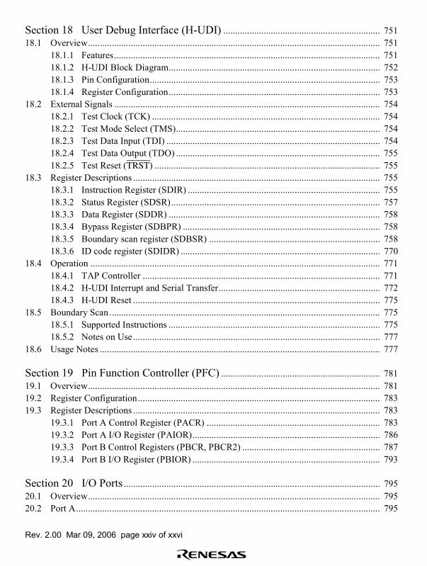
Section 18 User Debug Interface (H-UDI) .................................................................. 75118.1 Overview........................................................................................................................... 751
18.1.1 Features................................................................................................................ 75118.1.2 H-UDI Block Diagram......................................................................................... 75218.1.3 Pin Configuration................................................................................................. 75318.1.4 Register Configuration......................................................................................... 753
18.2 External Signals ................................................................................................................ 75418.2.1 Test Clock (TCK) ................................................................................................ 75418.2.2 Test Mode Select (TMS)...................................................................................... 75418.2.3 Test Data Input (TDI) .......................................................................................... 75418.2.4 Test Data Output (TDO) ...................................................................................... 75518.2.5 Test Reset (TRST) ............................................................................................... 755
18.3 Register Descriptions ........................................................................................................ 75518.3.1 Instruction Register (SDIR) ................................................................................. 75518.3.2 Status Register (SDSR)........................................................................................ 75718.3.3 Data Register (SDDR) ......................................................................................... 75818.3.4 Bypass Register (SDBPR) ................................................................................... 75818.3.5 Boundary scan register (SDBSR) ........................................................................ 75818.3.6 ID code register (SDIDR) .................................................................................... 770
18.4 Operation .......................................................................................................................... 77118.4.1 TAP Controller .................................................................................................... 77118.4.2 H-UDI Interrupt and Serial Transfer.................................................................... 77218.4.3 H-UDI Reset ........................................................................................................ 775
18.5 Boundary Scan .................................................................................................................. 77518.5.1 Supported Instructions ......................................................................................... 77518.5.2 Notes on Use........................................................................................................ 777
18.6 Usage Notes ...................................................................................................................... 777
Section 19 Pin Function Controller (PFC) ................................................................... 78119.1 Overview........................................................................................................................... 78119.2 Register Configuration...................................................................................................... 78319.3 Register Descriptions ........................................................................................................ 783
19.3.1 Port A Control Register (PACR) ......................................................................... 78319.3.2 Port A I/O Register (PAIOR)............................................................................... 78619.3.3 Port B Control Registers (PBCR, PBCR2) .......................................................... 78719.3.4 Port B I/O Register (PBIOR) ............................................................................... 793
Section 20 I/O Ports ............................................................................................................ 79520.1 Overview........................................................................................................................... 79520.2 Port A................................................................................................................................ 795

Rev. 2.00 Mar 09, 2006 page xxv of xxvi
20.2.1 Register Configuration......................................................................................... 79620.2.2 Port A Data Register (PADR) .............................................................................. 796
20.3 Port B ................................................................................................................................ 79720.3.1 Register Configuration......................................................................................... 79720.3.2 Port B Data Register (PBDR) .............................................................................. 798
Section 21 Power-Down Modes...................................................................................... 79921.1 Overview........................................................................................................................... 799
21.1.1 Power-Down Modes ............................................................................................ 79921.1.2 Register ................................................................................................................ 800
21.2 Register Descriptions ........................................................................................................ 80121.2.1 Standby Control Register 1 (SBYCR1) ............................................................... 80121.2.2 Standby Control Register 2 (SBYCR2) ............................................................... 803
21.3 Sleep Mode ....................................................................................................................... 80521.3.1 Transition to Sleep Mode..................................................................................... 80521.3.2 Canceling Sleep Mode ......................................................................................... 805
21.4 Standby Mode ................................................................................................................... 80521.4.1 Transition to Standby Mode................................................................................. 80521.4.2 Canceling Standby Mode ..................................................................................... 80721.4.3 Standby Mode Cancellation by NMI Interrupt..................................................... 80721.4.4 Clock Pause Function........................................................................................... 80821.4.5 Notes on Standby Mode....................................................................................... 811
21.5 Module Standby Function ................................................................................................. 81221.5.1 Transition to Module Standby Function............................................................... 81221.5.2 Clearing the Module Standby Function ............................................................... 812
Section 22 Electrical Characteristics.............................................................................. 81322.1 Absolute Maximum Ratings.............................................................................................. 81322.2 DC Characteristics ............................................................................................................ 81422.3 AC Characteristics ............................................................................................................ 816
22.3.1 Clock Timing ....................................................................................................... 81722.3.2 Control Signal Timing ......................................................................................... 82122.3.3 Bus Timing........................................................................................................... 82322.3.4 Direct Memory Access Controller Timing........................................................... 86122.3.5 Free-Running Timer Timing................................................................................ 86222.3.6 Serial Communication Interface Timing.............................................................. 86422.3.7 Watchdog Timer Timing...................................................................................... 86822.3.8 Serial I/O with FIFO / Serial I/O Timing............................................................. 86922.3.9 User Debug Interface Timing............................................................................... 87222.3.10 I/O Port Timing.................................................................................................... 873

Rev. 2.00 Mar 09, 2006 page xxvi of xxvi
22.3.11 Ethernet Controller Timing.................................................................................. 87522.3.12 STATS, BH, and BUSHiZ Signal Timing ........................................................... 878
22.4 AC Characteristic Test Conditions.................................................................................... 880
Appendix A On-Chip Peripheral Module Registers.................................................. 881A.1 Addresses .......................................................................................................................... 881
Appendix B Pin States ....................................................................................................... 900B.1 Pin States in Reset, Power-Down State, and Bus-Released State ..................................... 900
Appendix C Product Lineup............................................................................................. 904
Appendix D Package Dimensions .................................................................................. 905
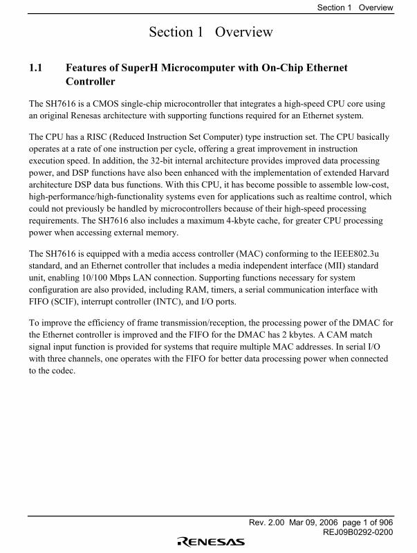
Section 1 Overview
Rev. 2.00 Mar 09, 2006 page 1 of 906REJ09B0292-0200
Section 1 Overview
1.1 Features of SuperH Microcomputer with On-Chip EthernetController
The SH7616 is a CMOS single-chip microcontroller that integrates a high-speed CPU core usingan original Renesas architecture with supporting functions required for an Ethernet system.
The CPU has a RISC (Reduced Instruction Set Computer) type instruction set. The CPU basicallyoperates at a rate of one instruction per cycle, offering a great improvement in instructionexecution speed. In addition, the 32-bit internal architecture provides improved data processingpower, and DSP functions have also been enhanced with the implementation of extended Harvardarchitecture DSP data bus functions. With this CPU, it has become possible to assemble low-cost,high-performance/high-functionality systems even for applications such as realtime control, whichcould not previously be handled by microcontrollers because of their high-speed processingrequirements. The SH7616 also includes a maximum 4-kbyte cache, for greater CPU processingpower when accessing external memory.
The SH7616 is equipped with a media access controller (MAC) conforming to the IEEE802.3ustandard, and an Ethernet controller that includes a media independent interface (MII) standardunit, enabling 10/100 Mbps LAN connection. Supporting functions necessary for systemconfiguration are also provided, including RAM, timers, a serial communication interface withFIFO (SCIF), interrupt controller (INTC), and I/O ports.
To improve the efficiency of frame transmission/reception, the processing power of the DMAC forthe Ethernet controller is improved and the FIFO for the DMAC has 2 kbytes. A CAM matchsignal input function is provided for systems that require multiple MAC addresses. In serial I/Owith three channels, one operates with the FIFO for better data processing power when connectedto the codec.
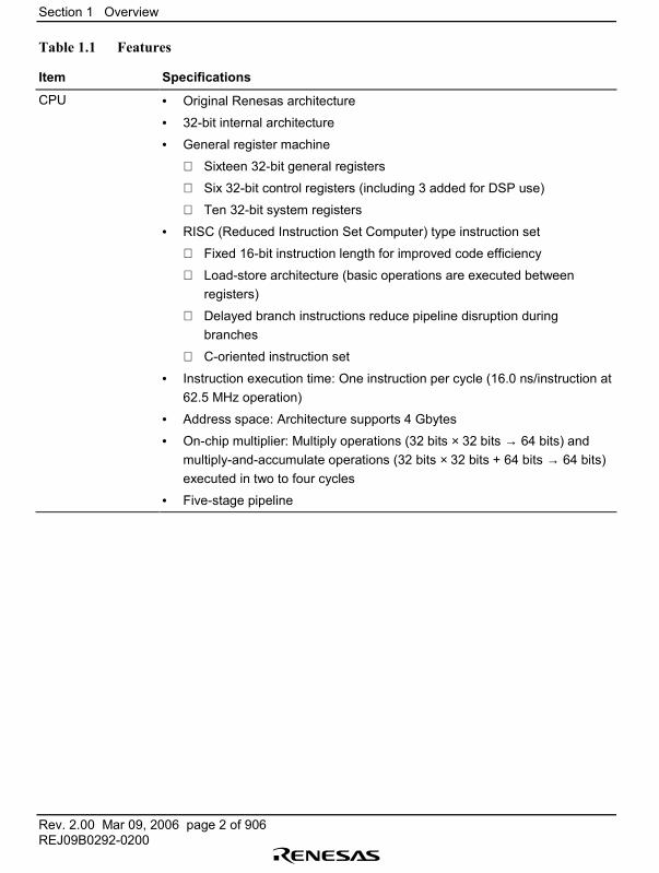
Section 1 Overview
Rev. 2.00 Mar 09, 2006 page 2 of 906REJ09B0292-0200
Table 1.1 Features
Item Specifications
CPU • Original Renesas architecture
• 32-bit internal architecture
• General register machine
Sixteen 32-bit general registers
Six 32-bit control registers (including 3 added for DSP use)
Ten 32-bit system registers
• RISC (Reduced Instruction Set Computer) type instruction set
Fixed 16-bit instruction length for improved code efficiency
Load-store architecture (basic operations are executed betweenregisters)
Delayed branch instructions reduce pipeline disruption duringbranches
C-oriented instruction set
• Instruction execution time: One instruction per cycle (16.0 ns/instruction at62.5 MHz operation)
• Address space: Architecture supports 4 Gbytes
• On-chip multiplier: Multiply operations (32 bits × 32 bits → 64 bits) andmultiply-and-accumulate operations (32 bits × 32 bits + 64 bits → 64 bits)executed in two to four cycles
• Five-stage pipeline
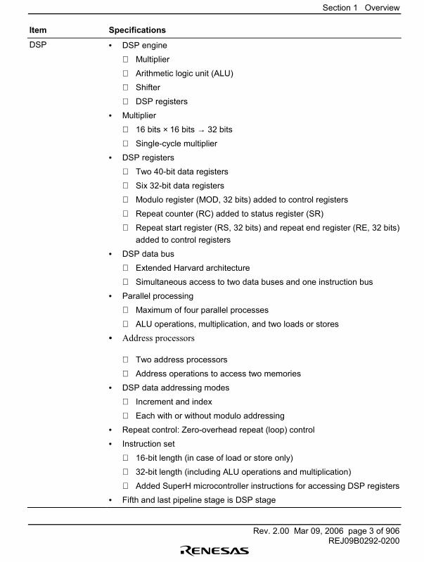
Section 1 Overview
Rev. 2.00 Mar 09, 2006 page 3 of 906REJ09B0292-0200
Item Specifications
DSP • DSP engine
Multiplier
Arithmetic logic unit (ALU)
Shifter
DSP registers
• Multiplier
16 bits × 16 bits → 32 bits
Single-cycle multiplier
• DSP registers
Two 40-bit data registers
Six 32-bit data registers
Modulo register (MOD, 32 bits) added to control registers
Repeat counter (RC) added to status register (SR)
Repeat start register (RS, 32 bits) and repeat end register (RE, 32 bits)added to control registers
• DSP data bus
Extended Harvard architecture
Simultaneous access to two data buses and one instruction bus
• Parallel processing
Maximum of four parallel processes
ALU operations, multiplication, and two loads or stores
• Address processors
Two address processors
Address operations to access two memories
• DSP data addressing modes
Increment and index
Each with or without modulo addressing
• Repeat control: Zero-overhead repeat (loop) control
• Instruction set
16-bit length (in case of load or store only)
32-bit length (including ALU operations and multiplication)
Added SuperH microcontroller instructions for accessing DSP registers
• Fifth and last pipeline stage is DSP stage
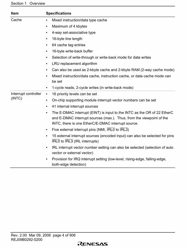
Section 1 Overview
Rev. 2.00 Mar 09, 2006 page 4 of 906REJ09B0292-0200
Item Specifications
Cache • Mixed instruction/data type cache
• Maximum of 4 kbytes
• 4-way set-associative type
• 16-byte line length
• 64 cache tag entries
• 16-byte write-back buffer
• Selection of write-through or write-back mode for data writes
• LRU replacement algorithm
• Can also be used as 2-kbyte cache and 2-kbyte RAM (2-way cache mode)
• Mixed instruction/data cache, instruction cache, or data cache mode canbe set
• 1-cycle reads, 2-cycle writes (in write-back mode)Interrupt controller(INTC)
• 16 priority levels can be set
• On-chip supporting module interrupt vector numbers can be set
• 41 internal interrupt sources
• The E-DMAC interrupt (EINT) is input to the INTC as the OR of 22 EtherCand E-DMAC interrupt sources (max.). Thus, from the viewpoint of theINTC, there is one EtherC/E-DMAC interrupt source.
• Five external interrupt pins (NMI, IRL0 to IRL3)
• 15 external interrupt sources (encoded input) can also be selected for pinsIRL0 to IRL3 (IRL interrupts)
• IRL interrupt vector number setting can also be selected (selection of autovector or external vector)
• Provision for IRQ interrupt setting (low-level, rising-edge, falling-edge,both-edge detection)

Section 1 Overview
Rev. 2.00 Mar 09, 2006 page 5 of 906REJ09B0292-0200
Item Specifications
User breakcontroller (UBC),4 channels(A, B, C, D)
• Interrupt generation based on independent or sequential conditions forchannels A, B, C, D
Three sequential setting patterns: A → B → C → D, B → C → D,C → D
• Settable break conditions: Address, data (channels C and D only), busmaster (CPU/DMAC), bus cycle (instruction fetch/data access), read/write,operand cycle (byte/word/longword)
• User break interrupt generated on occurrence of break condition
• Processing can be stopped before or after instruction execution ininstruction fetch cycle
• Break with specification of number of executions (channels C and D only)Settable number of executions: max. 212 � 1 (4095)
• PC trace function
Branch source/branch destination can be traced in branch instruction fetch(max. 8 addresses (4 pairs))

Section 1 Overview
Rev. 2.00 Mar 09, 2006 page 6 of 906REJ09B0292-0200
Item Specifications
Bus state controller(BSC)
• Address space divided into five areas (CS0 to CS4, max. linear 32 Mbyteseach)
Memory types such as DRAM, synchronous DRAM, burst ROM, canbe specified for each area
Two synchronous DRAM spaces (CS2, CS3); CS3 also supportsDRAM
Bus width (8, 16, 32 bits) can be selected for each area
Wait state insertion control for each area
Control signal output for each area
Endian can be set for CS2 and CS4
• Cache
Cache area/cache-through area selection by access address
Selection of write-through or write-back mode
• Refresh functions
CAS-before-RAS refreshing (auto refreshing) or self-refreshing
Refresh interval settable by means of refresh counter and clock selectsetting
Concentrated refreshing according to refresh count setting(1, 2, 4, 6, 8)
Refresh request output possible (REFOUT)
• Direct DRAM interface
Multiplexed row address/column address output
Fast page mode burst transfer and continuous access when reading
EDO mode
TP cycle generation to secure RAS precharge time
• Direct synchronous DRAM interface
Multiplexed row address/column address output
Bank-active mode (valid for CS3 only)
Selection of burst read/single write mode or burst read/burst writemode
• Bus arbitration (BRLS, BGR)
• Refresh counter can be used as interval timer
Interrupt request generated on compare match (CMI interrupt requestsignal)
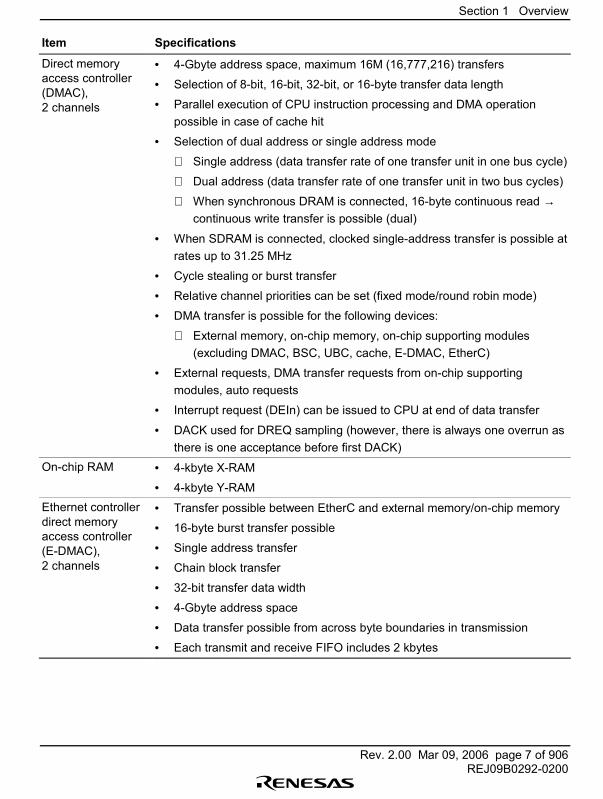
Section 1 Overview
Rev. 2.00 Mar 09, 2006 page 7 of 906REJ09B0292-0200
Item Specifications
Direct memoryaccess controller(DMAC),2 channels
• 4-Gbyte address space, maximum 16M (16,777,216) transfers
• Selection of 8-bit, 16-bit, 32-bit, or 16-byte transfer data length
• Parallel execution of CPU instruction processing and DMA operationpossible in case of cache hit
• Selection of dual address or single address mode
Single address (data transfer rate of one transfer unit in one bus cycle)
Dual address (data transfer rate of one transfer unit in two bus cycles)
When synchronous DRAM is connected, 16-byte continuous read →continuous write transfer is possible (dual)
• When SDRAM is connected, clocked single-address transfer is possible atrates up to 31.25 MHz
• Cycle stealing or burst transfer
• Relative channel priorities can be set (fixed mode/round robin mode)
• DMA transfer is possible for the following devices:
External memory, on-chip memory, on-chip supporting modules(excluding DMAC, BSC, UBC, cache, E-DMAC, EtherC)
• External requests, DMA transfer requests from on-chip supportingmodules, auto requests
• Interrupt request (DEIn) can be issued to CPU at end of data transfer
• DACK used for DREQ sampling (however, there is always one overrun asthere is one acceptance before first DACK)
On-chip RAM • 4-kbyte X-RAM
• 4-kbyte Y-RAMEthernet controllerdirect memoryaccess controller(E-DMAC),2 channels
• Transfer possible between EtherC and external memory/on-chip memory
• 16-byte burst transfer possible
• Single address transfer
• Chain block transfer
• 32-bit transfer data width
• 4-Gbyte address space
• Data transfer possible from across byte boundaries in transmission
• Each transmit and receive FIFO includes 2 kbytes
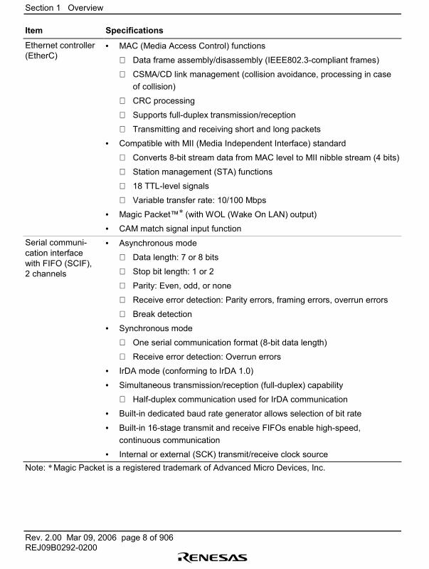
Section 1 Overview
Rev. 2.00 Mar 09, 2006 page 8 of 906REJ09B0292-0200
Item Specifications
Ethernet controller(EtherC)
• MAC (Media Access Control) functions
Data frame assembly/disassembly (IEEE802.3-compliant frames)
CSMA/CD link management (collision avoidance, processing in caseof collision)
CRC processing
Supports full-duplex transmission/reception
Transmitting and receiving short and long packets
• Compatible with MII (Media Independent Interface) standard
Converts 8-bit stream data from MAC level to MII nibble stream (4 bits)
Station management (STA) functions
18 TTL-level signals
Variable transfer rate: 10/100 Mbps
• Magic Packet�* (with WOL (Wake On LAN) output)
• CAM match signal input functionSerial communi-cation interfacewith FIFO (SCIF),2 channels
• Asynchronous mode
Data length: 7 or 8 bits
Stop bit length: 1 or 2
Parity: Even, odd, or none
Receive error detection: Parity errors, framing errors, overrun errors
Break detection
• Synchronous mode
One serial communication format (8-bit data length)
Receive error detection: Overrun errors
• IrDA mode (conforming to IrDA 1.0)
• Simultaneous transmission/reception (full-duplex) capability
Half-duplex communication used for IrDA communication
• Built-in dedicated baud rate generator allows selection of bit rate
• Built-in 16-stage transmit and receive FIFOs enable high-speed,continuous communication
• Internal or external (SCK) transmit/receive clock sourceNote: * Magic Packet is a registered trademark of Advanced Micro Devices, Inc.

Section 1 Overview
Rev. 2.00 Mar 09, 2006 page 9 of 906REJ09B0292-0200
Item Specifications
Serial communi-cation interfacewith FIFO (SCIF),2 channels
• Four interrupt sources
Transmit FIFO data empty
Break
Receive FIFO data full
Receive error
• Built-in modem control functions (RTS, CTS)
• Detection of transmit and receive FIFO register data quantity and numberof receive FIFO register transmit data errors
• Timeout error (DR) can be detected during receptionSerial I/O with FIFO(SIOF)
• Full-duplex operation (independent transmit and receive registers, andindependent transmit and receive clocks)
• Transmit and receive FIFO for primary data/transmit and receive buffer forcontrol data (enabling continuous transmission/reception)
• Interval transfer mode and continuous transfer mode
• Choice of 8- or 16-bit data length
• Data transfer communication by means of polling or interrupts
• Choice of MSB- or LSB-first transfer for data I/OSerial I/O (SIO),2 channels
• Full-duplex operation (independent transmit and receive registers, andindependent transmit and receive clocks)
• Transmit/receive ports with double-buffer structure (enabling continuoustransmission/reception)
• Interval transfer mode and continuous transfer mode
• Choice of 8- or 16-bit data length
• Data transfer communication by means of polling or interrupts
• MSB-first transfer between SIO and data I/O
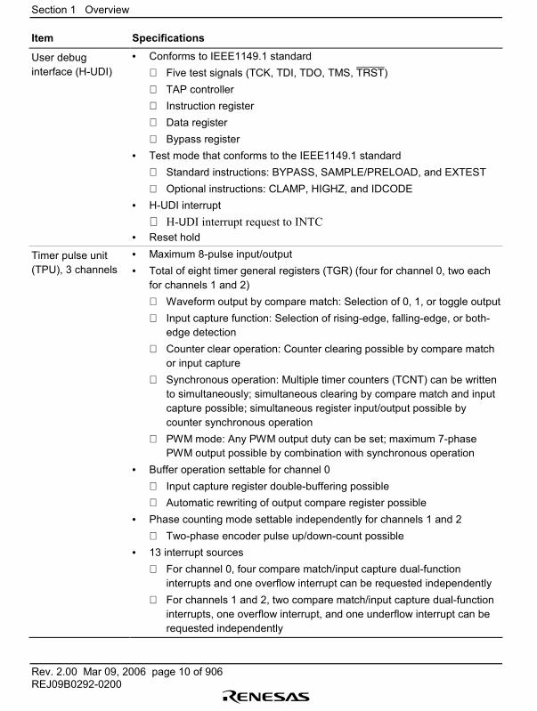
Section 1 Overview
Rev. 2.00 Mar 09, 2006 page 10 of 906REJ09B0292-0200
Item Specifications
User debuginterface (H-UDI)
• Conforms to IEEE1149.1 standard Five test signals (TCK, TDI, TDO, TMS, TRST) TAP controller Instruction register Data register Bypass register
• Test mode that conforms to the IEEE1149.1 standard Standard instructions: BYPASS, SAMPLE/PRELOAD, and EXTEST Optional instructions: CLAMP, HIGHZ, and IDCODE
• H-UDI interrupt H-UDI interrupt request to INTC
• Reset hold
Timer pulse unit(TPU), 3 channels
• Maximum 8-pulse input/output• Total of eight timer general registers (TGR) (four for channel 0, two each
for channels 1 and 2) Waveform output by compare match: Selection of 0, 1, or toggle output Input capture function: Selection of rising-edge, falling-edge, or both-
edge detection Counter clear operation: Counter clearing possible by compare match
or input capture Synchronous operation: Multiple timer counters (TCNT) can be written
to simultaneously; simultaneous clearing by compare match and inputcapture possible; simultaneous register input/output possible bycounter synchronous operation
PWM mode: Any PWM output duty can be set; maximum 7-phasePWM output possible by combination with synchronous operation
• Buffer operation settable for channel 0 Input capture register double-buffering possible Automatic rewriting of output compare register possible
• Phase counting mode settable independently for channels 1 and 2 Two-phase encoder pulse up/down-count possible
• 13 interrupt sources For channel 0, four compare match/input capture dual-function
interrupts and one overflow interrupt can be requested independently For channels 1 and 2, two compare match/input capture dual-function
interrupts, one overflow interrupt, and one underflow interrupt can berequested independently
Section 1 Overview
Rev. 2.00 Mar 09, 2006 page 11 of 906REJ09B0292-0200
Item Specifications
16-bit free-runningtimer (FRT),1 channel
• Choice of four counter input clocks
Three internal clocks (Pφ/8, Pφ/32, Pφ/128)
External clock (enabling external event counting)
• Two independent comparators (allowing generation of two waveformoutputs)
• Input capture (choice of rising edge or falling edge)
• Counter clear specification
Counter value can be cleared by compare match A
• Four interrupt sources
Two compare match sources (OCIA, OCIB)
One input capture source (ICI)
One overflow source (OVI)Watchdog timer(WDT), 1 channel
• Can be switched between watchdog timer mode and interval timer mode
• Internal reset, external signal (WDTOVF), or interrupt generated on countoverflow
• Used when standby mode is cleared or the clock frequency is changed,and in clock pause mode
• Selection of eight counter input clocksClock pulsegenerator (CPG)
• Built-in clock pulse generator
• Selection of crystal or external clock as clock source
• Built-in clock-multiplication PLL circuits
• Built-in PLL circuit for phase synchronization between external clock andinternal clock
• CPU/DSP core clock (Iφ), peripheral module clock (Pφ), and externalinterface clock (Eφ) frequencies can be scaled independently
Section 1 Overview
Rev. 2.00 Mar 09, 2006 page 12 of 906REJ09B0292-0200
Item Specifications
System controller(SYSC)
• Selection of seven operating mode settings, three power-down modes
• Operating modes
Control the method of clock generation (PLL ON/OFF) and clockdivision ratio
• Power-down mode
Sleep mode: CPU functions halted
Standby mode: All functions halted
Module standby function: Operation of FRT, SCIF, DMAC, UBC, DSP,TPU, and SIO on-chip supporting modules is halted selectively
I/O ports • 29 input/output ports
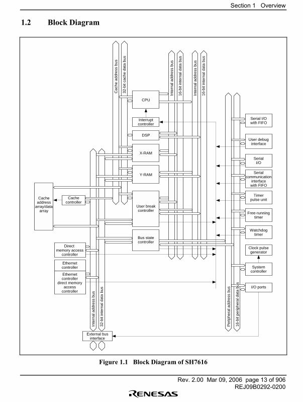
Section 1 Overview
Rev. 2.00 Mar 09, 2006 page 13 of 906REJ09B0292-0200
1.2 Block Diagram
CPU
X-RAM
Y-RAM
Bus statecontroller
User breakcontroller
Interruptcontroller
Cacheaddress
array/dataarray
DSP
Direct memory access
controller
Ethernetcontroller
direct memoryaccess
controller
Ethernetcontroller
External businterface
Cachecontroller
User debuginterface
SerialI/O
Timerpulse unit
Watchdogtimer
Clock pulsegenerator
Free-runningtimer
Serialcommunication
interfacewith FIFO
Systemcontroller
Cac
he a
ddre
ss b
us
Inte
rnal
add
ress
bus
Inte
rnal
add
ress
bus
Per
iphe
ral a
ddre
ss b
us
Inte
rnal
add
ress
bus
32-b
it in
tern
al d
ata
bus
32-b
it ca
che
data
bus
16-b
it in
tern
al d
ata
bus
16-b
it in
tern
al d
ata
bus
I/O ports
16-b
it pe
riphe
ral d
ata
bus
Serial I/Owith FIFO
Figure 1.1 Block Diagram of SH7616
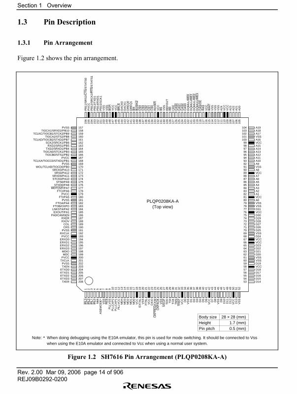
Section 1 Overview
Rev. 2.00 Mar 09, 2006 page 14 of 906REJ09B0292-0200
1.3 Pin Description
1.3.1 Pin Arrangement
Figure 1.2 shows the pin arrangement.
156
155
154
153
152
151
150
149
148
147
146
145
144
143
142
141
140
139
138
137
136
135
134
133
132
131
130
129
128
127
126
125
124
123
122
121
120
119
118
117
116
115
114
113
112
111
110
109
108
107
106
105
PB
11/S
RS
2/C
TS
/ST
AT
S0
PV
CC
PB
12/S
RC
K2/
RT
S/S
TA
TS
1P
B13
/TX
D1
PB
14/R
XD
1P
B15
/SC
K1
VS
SV
SS
BG
RV
CC
VC
CB
RL
SD
AC
K0
DA
CK
1D
RE
Q0
DR
EQ
1B
HB
US
HiZ
CS
4C
S3
CS
2C
S1
CS
0R
D/W
RV
CC
BS
VS
SR
EF
OU
TR
DC
KE
CA
S0
CA
S1
CA
S2
CA
S3
DQ
MLL
/WE
0D
QM
LU/W
E1
DQ
MU
L/W
E2
DQ
MU
U/W
E3
CA
S/O
ER
AS
VC
CW
AIT
VS
SV
SS
VS
SA
24V
CC
VC
CA
23A
22A
21A
20
1 2 3 4 5 6 7 8 9 10 11 12 13 14 15 16 17 18 19 20 21 22 23 24 25 26 27 28 29 30 31 32 33 34 35 36 37 38 39 40 41 42 43 44 45 46 47 48 49 50 51 52
IRL
3IR
L2
IRL
1IR
L0
NM
IA
SE
MO
DE
*V
SS
RE
SP
LLV
SS
PLL
CA
P2
PLL
CA
P1
PLL
VC
CM
D4
MD
3M
D2
MD
1M
D0
VC
CE
XT
AL
VS
SX
TA
LV
CC
CK
IOC
KP
RE
Q/C
KM
CK
PA
CK
VS
SIV
EC
FT
DO
TD
IT
CK
TM
ST
RS
TV
CC D0
VS
SD
1D
2D
3D
4D
5D
6V
CC D7
D8
VS
SD
9D
10D
11D
12V
CC
D13
VS
S
A19A18A17VSSA16VCCA15A14A13A12A11A10A9VSSA8VCCA7A6A5A4A3A2A1VCCA0VSSVSSD31VCCD30D29D28D27D26D25VSSD24VCCVCCD23D22D21D20VSSVSSD19VCCD18D17D16D15D14
104103102101100
9998979695949392919089888786858483828180797877767574737271706968676665646362616059585756555453
157158159160161162163164165166167168169170171172173174175176177178179180181182183184185186187188189190191192193194195196197198199200201202203204205206207208
PVSSTIOCA1/SRXD2/PB10
TCLKC/TIOCB1/STCK2/PB9TIOCA2/STS2/PB8
TCLKD/TIOCB2/STXD2/PB7SCK2/SRCK1/PB6
RXD2/SRS1/PB5TXD2/SRXD1/PB4
TIOCA0/STCK1/PB3TIOCB0/STS1/PB2
PVCCTCLKA/TIOCC0/STXD1/PB1
PVSSWOL/TCLKB/TIOCD0/PB0
SRCK0/PA13SRS0/PA12
SRXD0/PA11STCK0/PA10
STS0/PA9STXD0/PA8
WDTOVF/PA7FTCI/PA6
PVCCFTI/PA5
PVSSFTOA/PA4
FTOB/CKPOLNKSTA/PA2EXOUT/PA1
PA0/CAMSENRXERRXDV
COLCRS
PVSSRXCLKPVCC
ERXD0ERXD1ERXD2ERXD3
MDIOMDC
PVCCTXCLKPVSSTXEN
ETXD0ETXD1ETXD2ETXD3TXER
PLQP0208KA-A(Top view)
Body sizeHeightPin pitch
Note: * When doing debugging using the E10A emulator, this pin is used for mode switching. It should be connected to Vss when using the E10A emulator and connected to Vcc when using a normal user system.
28 × 281.70.5
(mm)(mm)(mm)
Figure 1.2 SH7616 Pin Arrangement (PLQP0208KA-A)
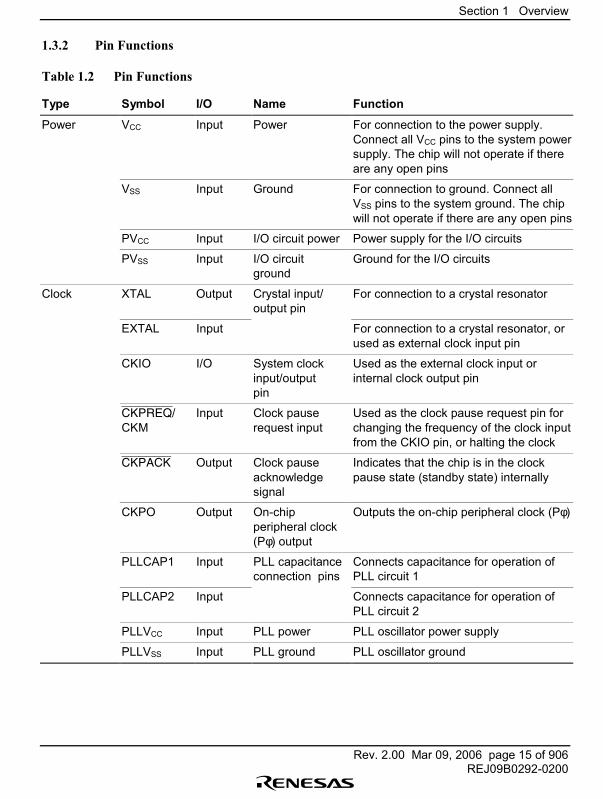
Section 1 Overview
Rev. 2.00 Mar 09, 2006 page 15 of 906REJ09B0292-0200
1.3.2 Pin Functions
Table 1.2 Pin Functions
Type Symbol I/O Name Function
Power VCC Input Power For connection to the power supply.Connect all VCC pins to the system powersupply. The chip will not operate if thereare any open pins
VSS Input Ground For connection to ground. Connect allVSS pins to the system ground. The chipwill not operate if there are any open pins
PVCC Input I/O circuit power Power supply for the I/O circuits
PVSS Input I/O circuitground
Ground for the I/O circuits
Clock XTAL Output Crystal input/output pin
For connection to a crystal resonator
EXTAL Input For connection to a crystal resonator, orused as external clock input pin
CKIO I/O System clockinput/outputpin
Used as the external clock input orinternal clock output pin
CKPREQ/CKM
Input Clock pauserequest input
Used as the clock pause request pin forchanging the frequency of the clock inputfrom the CKIO pin, or halting the clock
CKPACK Output Clock pauseacknowledgesignal
Indicates that the chip is in the clockpause state (standby state) internally
CKPO Output On-chipperipheral clock(Pφ) output
Outputs the on-chip peripheral clock (Pφ)
PLLCAP1 Input PLL capacitanceconnection pins
Connects capacitance for operation ofPLL circuit 1
PLLCAP2 Input Connects capacitance for operation ofPLL circuit 2
PLLVCC Input PLL power PLL oscillator power supply
PLLVSS Input PLL ground PLL oscillator ground
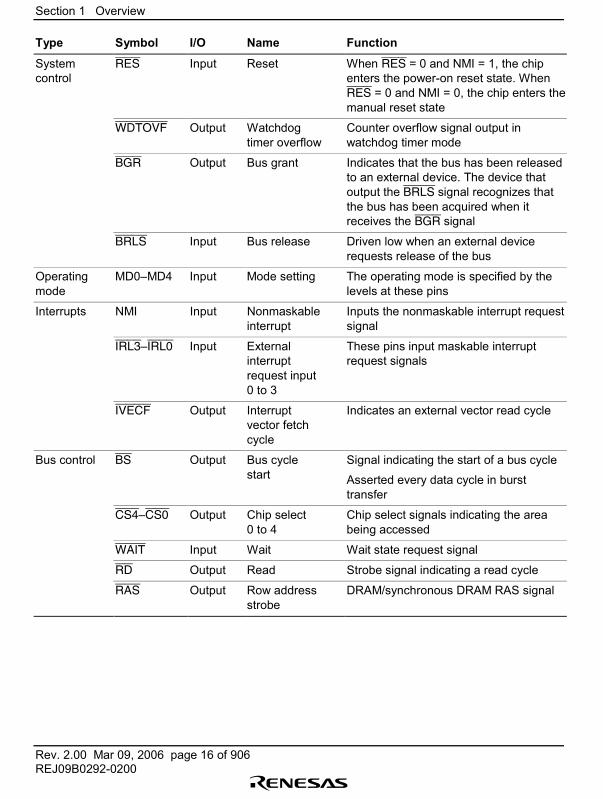
Section 1 Overview
Rev. 2.00 Mar 09, 2006 page 16 of 906REJ09B0292-0200
Type Symbol I/O Name Function
Systemcontrol
RES Input Reset When RES = 0 and NMI = 1, the chipenters the power-on reset state. WhenRES = 0 and NMI = 0, the chip enters themanual reset state
WDTOVF Output Watchdogtimer overflow
Counter overflow signal output inwatchdog timer mode
BGR Output Bus grant Indicates that the bus has been releasedto an external device. The device thatoutput the BRLS signal recognizes thatthe bus has been acquired when itreceives the BGR signal
BRLS Input Bus release Driven low when an external devicerequests release of the bus
Operatingmode
MD0�MD4 Input Mode setting The operating mode is specified by thelevels at these pins
Interrupts NMI Input Nonmaskableinterrupt
Inputs the nonmaskable interrupt requestsignal
IRL3�IRL0 Input Externalinterruptrequest input0 to 3
These pins input maskable interruptrequest signals
IVECF Output Interruptvector fetchcycle
Indicates an external vector read cycle
Bus control BS Output Bus cyclestart
Signal indicating the start of a bus cycle
Asserted every data cycle in bursttransfer
CS4�CS0 Output Chip select0 to 4
Chip select signals indicating the areabeing accessed
WAIT Input Wait Wait state request signal
RD Output Read Strobe signal indicating a read cycle
RAS Output Row addressstrobe
DRAM/synchronous DRAM RAS signal
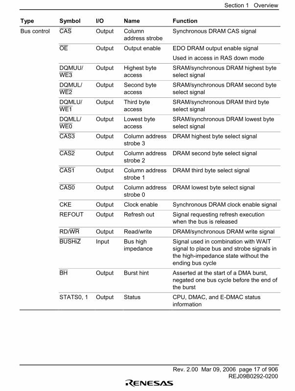
Section 1 Overview
Rev. 2.00 Mar 09, 2006 page 17 of 906REJ09B0292-0200
Type Symbol I/O Name Function
Bus control CAS Output Columnaddress strobe
Synchronous DRAM CAS signal
OE Output Output enable EDO DRAM output enable signal
Used in access in RAS down mode
DQMUU/WE3
Output Highest byteaccess
SRAM/synchronous DRAM highest byteselect signal
DQMUL/WE2
Output Second byteaccess
SRAM/synchronous DRAM second byteselect signal
DQMLU/WE1
Output Third byteaccess
SRAM/synchronous DRAM third byteselect signal
DQMLL/WE0
Output Lowest byteaccess
SRAM/synchronous DRAM lowest byteselect signal
CAS3 Output Column addressstrobe 3
DRAM highest byte select signal
CAS2 Output Column addressstrobe 2
DRAM second byte select signal
CAS1 Output Column addressstrobe 1
DRAM third byte select signal
CAS0 Output Column addressstrobe 0
DRAM lowest byte select signal
CKE Output Clock enable Synchronous DRAM clock enable signal
REFOUT Output Refresh out Signal requesting refresh executionwhen the bus is released
RD/WR Output Read/write DRAM/synchronous DRAM write signal
BUSHiZ Input Bus highimpedance
Signal used in combination with WAITsignal to place bus and strobe signals inthe high-impedance state without theending bus cycle
BH Output Burst hint Asserted at the start of a DMA burst,negated one bus cycle before the end ofthe burst
STATS0, 1 Output Status CPU, DMAC, and E-DMAC statusinformation
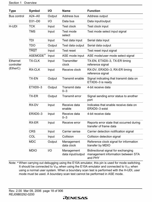
Section 1 Overview
Rev. 2.00 Mar 09, 2006 page 18 of 906REJ09B0292-0200
Type Symbol I/O Name Function
Bus control A24�A0 Output Address bus Address output
D31�D0 I/O Data bus Data input/output
H-UDI TCK Input Test clock Test clock input
TMS Input Test modeselect
Test mode select input signal
TDI Input Test data input Serial data input
TDO Output Test data output Serial data output
TRST Input Test reset Test reset input signal
ASEMODE* Input ASE mode input ASE mode/user mode select signal
Ethernetcontroller
TX-CLK Input Transmitterclock
TX-EN, ETXD0�3, TX-ER timingreference signal
(EtherC) RX-CLK Input Receive clock RX-DV, ERXD0�3, RX-ER timingreference signal
TX-EN Output Transmit enable Signal indicating that transmit data onETXD0�3 is ready
ETXD0�3 Output Transmit data0�3
4-bit receive data
TX-ER Output Transmit error Signal sending error status to anotherport
RX-DV Input Receive dataenable
Indicates that enable receive data onERXD0�3 exist
ERXD0�3 Input Receive data0�3
4-bit receive data
RX-ER Input Receive error Reports error state that occurred duringtransfer of frame data
CRS Input Carrier sense Carrier detection notification signal
COL Input Collision Collision detection signal
MDC Output Managementdata clock
Reference clock signal for informationtransfer by MDIO
MDIO I/O Managementdata input/output
Bidirectional signal for exchangingmanagement information between STAand PHY
Note: * When carrying out debugging using the E10A emulator, this pin is used for mode switching.It should be connected to VSS when using the E10A emulator and connected to VCC whenusing a normal user system. When a boundary scan test is performed with the H-UDI, usermode must be used. A boundary scan test cannot be performed in ASE mode.
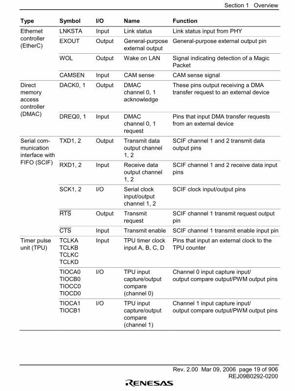
Section 1 Overview
Rev. 2.00 Mar 09, 2006 page 19 of 906REJ09B0292-0200
Type Symbol I/O Name Function
Ethernet LNKSTA Input Link status Link status input from PHYcontroller(EtherC)
EXOUT Output General-purposeexternal output
General-purpose external output pin
WOL Output Wake on LAN Signal indicating detection of a MagicPacket
CAMSEN Input CAM sense CAM sense signal
Directmemoryaccesscontroller
DACK0, 1 Output DMACchannel 0, 1acknowledge
These pins output receiving a DMAtransfer request to an external device
(DMAC) DREQ0, 1 Input DMACchannel 0, 1request
Pins that input DMA transfer requestsfrom an external device
Serial com-municationinterface with
TXD1, 2 Output Transmit dataoutput channel1, 2
SCIF channel 1 and 2 transmit dataoutput pins
FIFO (SCIF) RXD1, 2 Input Receive dataoutput channel1, 2
SCIF channel 1 and 2 receive data inputpins
SCK1, 2 I/O Serial clockinput/outputchannel 1, 2
SCIF clock input/output pins
RTS Output Transmitrequest
SCIF channel 1 transmit request outputpin
CTS Input Transmit enable SCIF channel 1 transmit enable input pin
Timer pulseunit (TPU)
TCLKATCLKBTCLKCTCLKD
Input TPU timer clockinput A, B, C, D
Pins that input an external clock to theTPU counter
TIOCA0TIOCB0TIOCC0TIOCD0
I/O TPU inputcapture/outputcompare(channel 0)
Channel 0 input capture input/output compare output/PWM output pins
TIOCA1TIOCB1
I/O TPU inputcapture/outputcompare(channel 1)
Channel 1 input capture input/output compare output/PWM output pins
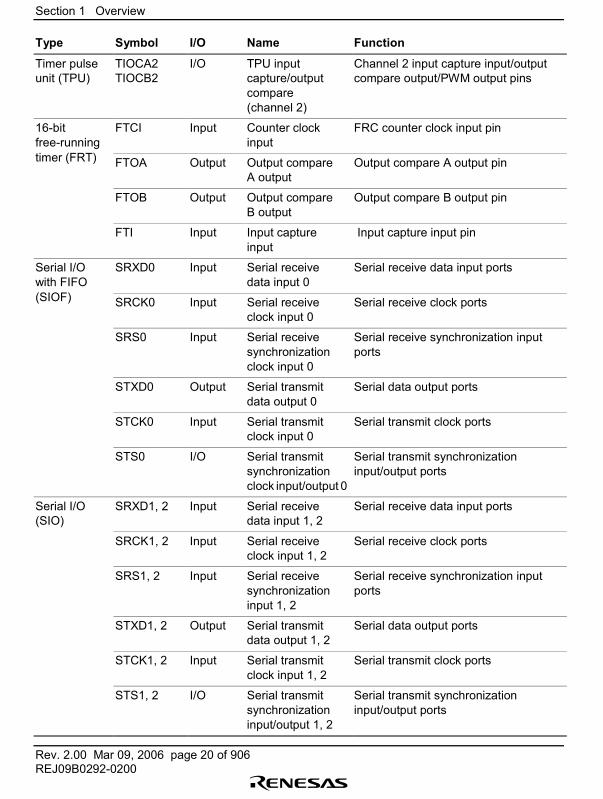
Section 1 Overview
Rev. 2.00 Mar 09, 2006 page 20 of 906REJ09B0292-0200
Type Symbol I/O Name Function
Timer pulseunit (TPU)
TIOCA2TIOCB2
I/O TPU inputcapture/outputcompare(channel 2)
Channel 2 input capture input/outputcompare output/PWM output pins
16-bitfree-running
FTCI Input Counter clockinput
FRC counter clock input pin
timer (FRT) FTOA Output Output compareA output
Output compare A output pin
FTOB Output Output compareB output
Output compare B output pin
FTI Input Input captureinput
Input capture input pin
Serial I/Owith FIFO
SRXD0 Input Serial receivedata input 0
Serial receive data input ports
(SIOF) SRCK0 Input Serial receiveclock input 0
Serial receive clock ports
SRS0 Input Serial receivesynchronizationclock input 0
Serial receive synchronization inputports
STXD0 Output Serial transmitdata output 0
Serial data output ports
STCK0 Input Serial transmitclock input 0
Serial transmit clock ports
STS0 I/O Serial transmitsynchronizationclock input/output 0
Serial transmit synchronizationinput/output ports
Serial I/O(SIO)
SRXD1, 2 Input Serial receivedata input 1, 2
Serial receive data input ports
SRCK1, 2 Input Serial receiveclock input 1, 2
Serial receive clock ports
SRS1, 2 Input Serial receivesynchronizationinput 1, 2
Serial receive synchronization inputports
STXD1, 2 Output Serial transmitdata output 1, 2
Serial data output ports
STCK1, 2 Input Serial transmitclock input 1, 2
Serial transmit clock ports
STS1, 2 I/O Serial transmitsynchronizationinput/output 1, 2
Serial transmit synchronizationinput/output ports
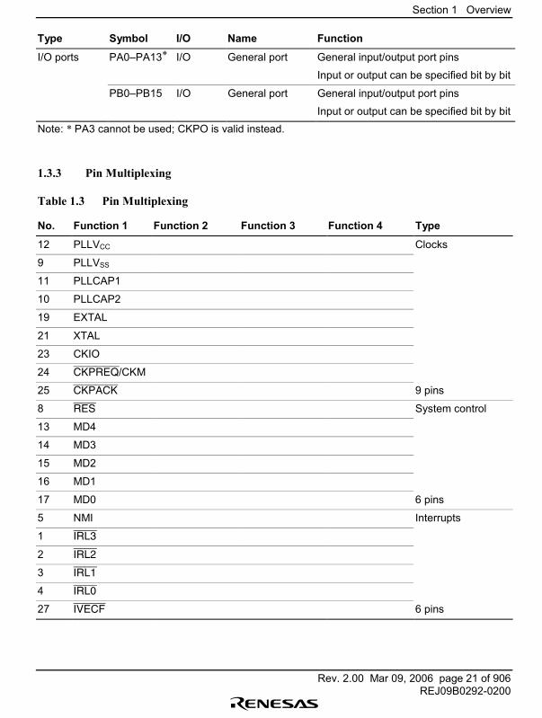
Section 1 Overview
Rev. 2.00 Mar 09, 2006 page 21 of 906REJ09B0292-0200
Type Symbol I/O Name Function
I/O ports PA0�PA13* I/O General port General input/output port pins
Input or output can be specified bit by bit
PB0�PB15 I/O General port General input/output port pins
Input or output can be specified bit by bitNote: * PA3 cannot be used; CKPO is valid instead.
1.3.3 Pin Multiplexing
Table 1.3 Pin Multiplexing
No. Function 1 Function 2 Function 3 Function 4 Type
12 PLLVCC Clocks
9 PLLVSS
11 PLLCAP1
10 PLLCAP2
19 EXTAL
21 XTAL
23 CKIO
24 CKPREQ/CKM
25 CKPACK 9 pins
8 RES System control
13 MD4
14 MD3
15 MD2
16 MD1
17 MD0 6 pins
5 NMI Interrupts
1 IRL3
2 IRL2
3 IRL1
4 IRL0
27 IVECF 6 pins
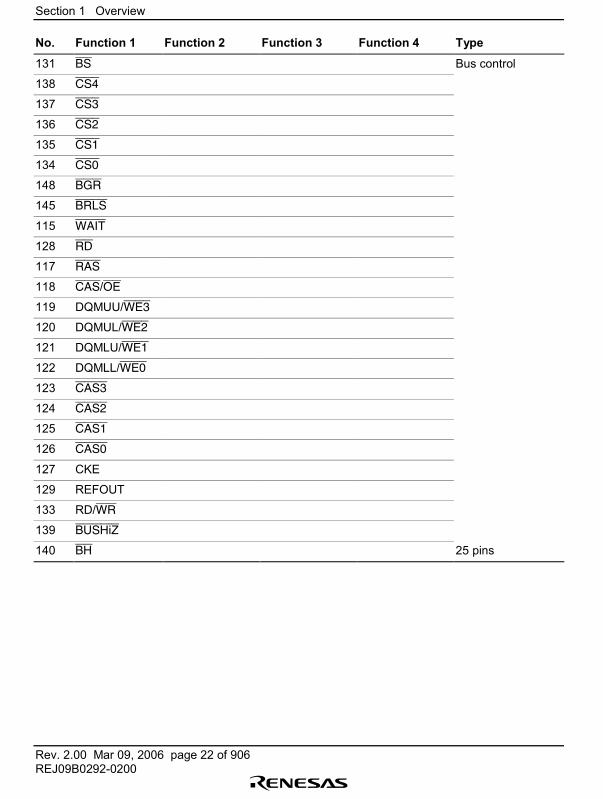
Section 1 Overview
Rev. 2.00 Mar 09, 2006 page 22 of 906REJ09B0292-0200
No. Function 1 Function 2 Function 3 Function 4 Type
131 BS Bus control
138 CS4
137 CS3
136 CS2
135 CS1
134 CS0
148 BGR
145 BRLS
115 WAIT
128 RD
117 RAS
118 CAS/OE
119 DQMUU/WE3
120 DQMUL/WE2
121 DQMLU/WE1
122 DQMLL/WE0
123 CAS3
124 CAS2
125 CAS1
126 CAS0
127 CKE
129 REFOUT
133 RD/WR
139 BUSHiZ
140 BH 25 pins
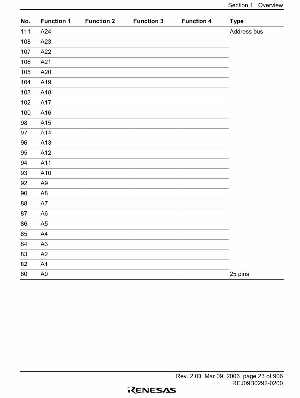
Section 1 Overview
Rev. 2.00 Mar 09, 2006 page 23 of 906REJ09B0292-0200
No. Function 1 Function 2 Function 3 Function 4 Type
111 A24 Address bus
108 A23
107 A22
106 A21
105 A20
104 A19
103 A18
102 A17
100 A16
98 A15
97 A14
96 A13
95 A12
94 A11
93 A10
92 A9
90 A8
88 A7
87 A6
86 A5
85 A4
84 A3
83 A2
82 A1
80 A0 25 pins
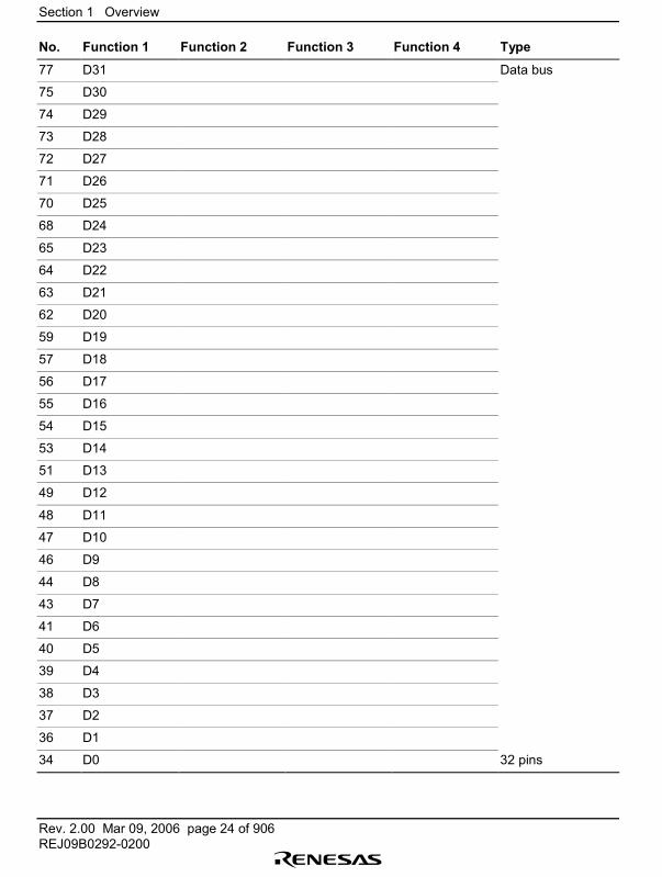
Section 1 Overview
Rev. 2.00 Mar 09, 2006 page 24 of 906REJ09B0292-0200
No. Function 1 Function 2 Function 3 Function 4 Type
77 D31 Data bus
75 D30
74 D29
73 D28
72 D27
71 D26
70 D25
68 D24
65 D23
64 D22
63 D21
62 D20
59 D19
57 D18
56 D17
55 D16
54 D15
53 D14
51 D13
49 D12
48 D11
47 D10
46 D9
44 D8
43 D7
41 D6
40 D5
39 D4
38 D3
37 D2
36 D1
34 D0 32 pins
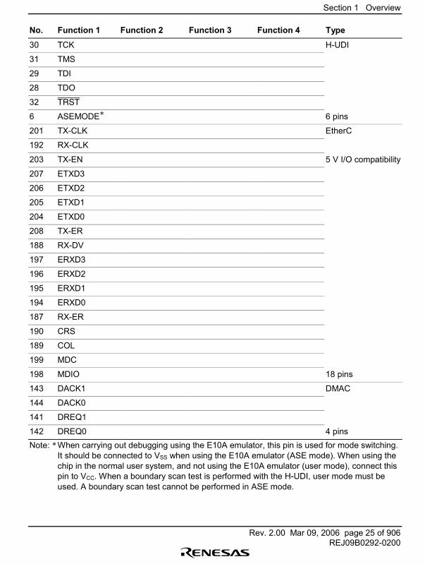
Section 1 Overview
Rev. 2.00 Mar 09, 2006 page 25 of 906REJ09B0292-0200
No. Function 1 Function 2 Function 3 Function 4 Type
30 TCK H-UDI
31 TMS
29 TDI
28 TDO
32 TRST
6 ASEMODE* 6 pins
201 TX-CLK EtherC
192 RX-CLK
203 TX-EN 5 V I/O compatibility
207 ETXD3
206 ETXD2
205 ETXD1
204 ETXD0
208 TX-ER
188 RX-DV
197 ERXD3
196 ERXD2
195 ERXD1
194 ERXD0
187 RX-ER
190 CRS
189 COL
199 MDC
198 MDIO 18 pins
143 DACK1 DMAC
144 DACK0
141 DREQ1
142 DREQ0 4 pinsNote: * When carrying out debugging using the E10A emulator, this pin is used for mode switching.
It should be connected to VSS when using the E10A emulator (ASE mode). When using thechip in the normal user system, and not using the E10A emulator (user mode), connect thispin to VCC. When a boundary scan test is performed with the H-UDI, user mode must beused. A boundary scan test cannot be performed in ASE mode.
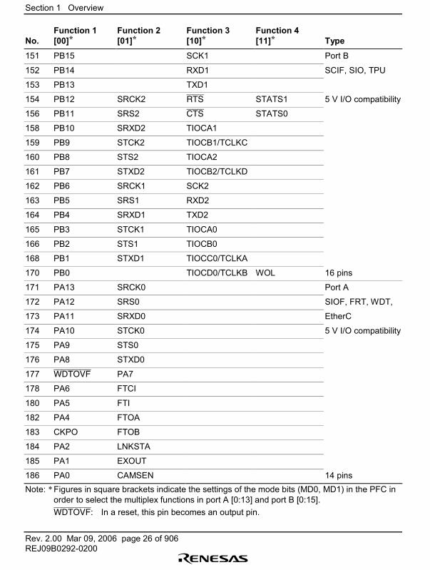
Section 1 Overview
Rev. 2.00 Mar 09, 2006 page 26 of 906REJ09B0292-0200
No.Function 1[00]*
Function 2[01]*
Function 3[10]*
Function 4[11]* Type
151 PB15 SCK1 Port B
152 PB14 RXD1 SCIF, SIO, TPU
153 PB13 TXD1
154 PB12 SRCK2 RTS STATS1 5 V I/O compatibility
156 PB11 SRS2 CTS STATS0
158 PB10 SRXD2 TIOCA1
159 PB9 STCK2 TIOCB1/TCLKC
160 PB8 STS2 TIOCA2
161 PB7 STXD2 TIOCB2/TCLKD
162 PB6 SRCK1 SCK2
163 PB5 SRS1 RXD2
164 PB4 SRXD1 TXD2
165 PB3 STCK1 TIOCA0
166 PB2 STS1 TIOCB0
168 PB1 STXD1 TIOCC0/TCLKA
170 PB0 TIOCD0/TCLKB WOL 16 pins
171 PA13 SRCK0 Port A
172 PA12 SRS0 SIOF, FRT, WDT,
173 PA11 SRXD0 EtherC
174 PA10 STCK0 5 V I/O compatibility
175 PA9 STS0
176 PA8 STXD0
177 WDTOVF PA7
178 PA6 FTCI
180 PA5 FTI
182 PA4 FTOA
183 CKPO FTOB
184 PA2 LNKSTA
185 PA1 EXOUT
186 PA0 CAMSEN 14 pinsNote: * Figures in square brackets indicate the settings of the mode bits (MD0, MD1) in the PFC in
order to select the multiplex functions in port A [0:13] and port B [0:15].WDTOVF: In a reset, this pin becomes an output pin.

Section 1 Overview
Rev. 2.00 Mar 09, 2006 page 27 of 906REJ09B0292-0200
When used for general input/output, attention must be paid to the polarity ofthis pin.
1.4 Processing States
State Transitions: The CPU has five processing states: the reset state, exception handling state,bus-released state, program execution state, and power-down state. Figure 1.3 shows the statetransitions.
RST = 0, NMI = 1
RST = 1,NMI = 0
RST = 1,NMI = 1
Interrupt or DMAaddress error
NMI interrupt
End of exception handling
Bus request
Exception
Bus request clearedBus request
received
Bus request cleared
SLEEPinstruction
(SBY = 0)
SLEEP instruction (SBY = 1)
From any state whenRES = 0 and NMI = 1
From any state whenRES = 0 and NMI = 0
Reset states
Power-down state
Note: * clock pause function
Bus request received
Bus requestcleared
RST = 0, NMI = 0
MSTPbit
cleared
MSTPbit set
Bus-released state
Exception-handling state
Manual reset statePower-on reset state
Program execution state
Sleep mode Standby mode
Module standby
SBY bit set and CKPREQ = 0*
CKPREQ = 1*
Figure 1.3 Processing State Transitions
Section 1 Overview
Rev. 2.00 Mar 09, 2006 page 28 of 906REJ09B0292-0200
• Reset StateIn this state, the CPU is reset. The reset state is entered when the RES pin goes low. Thepower-on reset state is entered if the NMI pin is high, and the manual reset state is entered ifthe NMI pin is low.
• Exception Handling StateThe exception handling state is a transient state that occurs when the CPU alters the normalprogramming flow dues to a reset, interrupt, or other exception handling source.In the case of a reset, the CPU fetches the execution start address as the initial value of theprogram counter (PC) from the exception vector table, and the initial value of the stack pointer(SP), stores these values, branches to the start address, and begins program execution at thataddress.In the case of an interrupt, etc., the CPU references the SP and saves the PC and status register(SR) in the stack area. It fetches the start address of the exception service routine from theexception vector table, branches to that address, and begins program execution.Subsequently, the processing state is the program execution state.
• Program Execution StateIn the program execution state the CPU executes program instructions in normal sequence.
• Power-Down StateIn the power-down state the CPU stops operating to conserve power. The power-down state isentered by executing a SLEEP instruction. The power-down state includes two modes�sleepmode and standby mode�and a module standby function.
• Bus-Released StateIn the bus-released state, the CPU releases the bus to a device that has requested it.
Power-Down State: In addition to the normal program execution state, another CPU processingstate called the power-down state is provided. In this state, CPU operation is halted and powerconsumption is reduced. The power-down state includes two modes�sleep mode and standbymode�and a module standby function.
• Sleep ModeA transition to sleep mode is made if the SLEEP instruction is executed while the standby bit(SBY) is cleared to 0 in standby control register 1 (SBYCR1). In sleep mode CPU operationsstop but data in the CPU�s internal registers and in on-chip cache memory and on-chip RAM isretained. The functions of the on-chip supporting modules do not stop.
Section 1 Overview
Rev. 2.00 Mar 09, 2006 page 29 of 906REJ09B0292-0200
• Standby ModeA transition to standby mode is made if the SLEEP instruction is executed while SBY is set to1 in SBYCR1. In standby mode the CPU, the on-chip modules, and the oscillator all stop.When entering standby mode, the DMAC�s DMA master enable bit should be cleared to 0.Also, the cache should be turned off before entering this mode. The contents of the cache andon-chip RAM are not retained in this mode.Standby mode is exited by means of a reset or an external NMI interrupt. When standby modeis exited, the normal program execution state is entered via the exception handling state afterthe elapse of the oscillation settling time.If a transition is made to standby mode using the clock pause function, it is possible to changethe frequency of the CKIO pin input clock, or to stop the clock itself. When SBY in SBYCR1is set to 1 and a low level is applied to the CKPREQ/CKM pin, a transition is made to standbymode and a low level is output from the CKPACK pin. The clock can then be stopped, or itsfrequency changed.On-chip supporting module states and pin states are the same as in the normal standby modeentered by means of the SLEEP instruction. A transition to the program execution state ismade by applying a high level to the CKPREQ/CKM pin.In this mode the oscillator is halted, greatly reducing power consumption.
• Module Standby FunctionA module standby function is provided for the following on-chip supporting modules: thedirect memory access controller (DMAC), DSP, 16-bit free-running timer (FRT), serialcommunication interface with FIFO (SCIF), serial I/O with FIFO (SIOF), serial I/O (SIO), userbreak controller (UBC), and timer pulse unit (TPU). A module standby function is notsupported for the Ethernet controller (EtherC) or the Ethernet direct memory access controller(E-DMAC).Setting one of module stop bits 11 to 3 and 1 (MSTP11 to MSTP3, MSTP1) to 1 in the standbycontrol register (SBYCR1/2) stops the clock supply to the corresponding on-chip supportingmodule. Use of this function enables power consumption to be reduced.The module standby function is cleared by clearing the corresponding MSTP bit to 0.DSP instructions must not be used when the DSP has been placed in the module standby state.When using the DMAC module standby function, the direct memory access controller�s DMAmaster enable bit should be cleared to 0.

Section 1 Overview
Rev. 2.00 Mar 09, 2006 page 30 of 906REJ09B0292-0200
Table 1.4 Power-Down State
State
ModeEnteringConditions Clock CPU
On-chipSupportingModules
CPURegisters
On-ChipCache orOn-ChipRAM
ExitingConditions
Sleepmode
ExecutingSLEEPinstructionwhile SBY bitis cleared inSBYCR1
Operating Halted Operating Held Held 1. Interrupt2. DMA address
error3. Power-on reset4. Manual reset
Standbymode
ExecutingSLEEPinstructionwhile SBYbit is set inSBYCR1
Halted Halted Halted andinitialized*1
Held Undefined 1. NMI interrupt2. Power-on reset3. Manual reset
Modulestandbyfunction
SettingMSTP bitcorrespondingto individualmodule
Operating Operating(DSPhalted)
Clock supplyto specifiedmodulehalted,moduleinitialized*2
Held Held 1. Clearing MSTPbit
2. Power-on reset3. Manual reset
Notes: 1. Depends on individual supporting module or pin.2. DMAC and DSP registers and specified module interrupt vectors retain their set values.
Section 2 CPU
Rev. 2.00 Mar 09, 2006 page 31 of 906REJ09B0292-0200
Section 2 CPU
2.1 Register Configuration
The register set consists of sixteen 32-bit general registers, six 32-bit control registers and ten 32-bit system registers.
This chip is upwardly compatible with the SH-1, SH-2 on the object code level. For this reason,several registers have been added to the previous SuperH microcontroller registers. The addedregisters are the three control registers: repeat start register (RS), repeat end register (RE), andmodulo register (MOD) and the six system registers: DSP status register (DSR), and A0, A1, X0,X1, Y0 and Y1 among the DSP data registers.
The general registers are used in the same manner as the SH-1, SH-2 with regard to SuperHmicrocontroller-type instructions. With regard to DSP type instructions, they are used as addressand index registers for accessing memory.
2.1.1 General Registers
There are 16 general registers (Rn) numbered R0�R15, which are 32 bits in length. Generalregisters are used for data processing and address calculation.
With SuperH microcomputer type instructions, R0 is also used as an index register. Severalinstructions are limited to use of R0 only. R15 is used as the hardware stack pointer (SP). Savingand recovering the status register (SR) and program counter (PC) in exception processing isaccomplished by referencing the stack using R15.
With DSP type instructions, eight of the 16 general registers are used for the addressing of X, Ydata memory and data memory (single data) using the I bus.
R4, R5 are used as an X address register (Ax) for X memory accesses, and R8 is used as an Xindex register (Ix). R6, R7 are used as a Y address register (Ay) for Y memory accesses, and R9 isused as a Y index register (Iy). R2, R3, R4, R5 are used as a single data address register (As) foraccessing single data using the I bus, and R8 is used as a single data index register (Is).
DSP type instructions can simultaneously access X and Y data memory. There are two groups ofaddress pointers for designating X and Y data memory addresses.
Figure 2.1 shows the general registers.
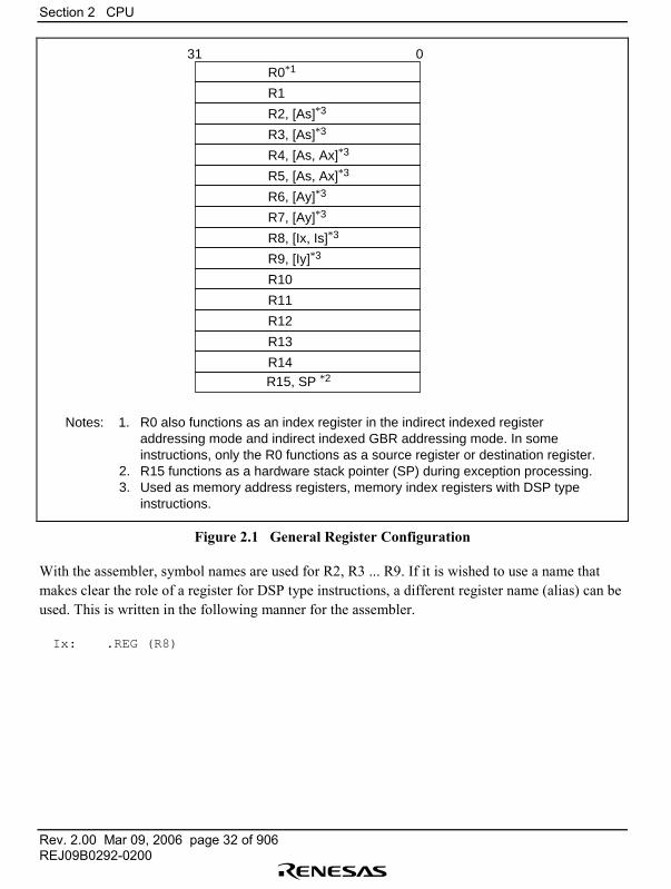
Section 2 CPU
Rev. 2.00 Mar 09, 2006 page 32 of 906REJ09B0292-0200
R0*1
R1
R2, [As]*3
R3, [As]*3
R4, [As, Ax]*3
R5, [As, Ax]*3
R6, [Ay]*3
R7, [Ay]*3
R8, [Ix, Is]*3
R9, [Iy]*3
R10
R11
R12
R13
R14R15, SP *2
031
R0 also functions as an index register in the indirect indexed register addressing mode and indirect indexed GBR addressing mode. In some instructions, only the R0 functions as a source register or destination register.R15 functions as a hardware stack pointer (SP) during exception processing.Used as memory address registers, memory index registers with DSP type instructions.
Notes: 1.
2.3.
Figure 2.1 General Register Configuration
With the assembler, symbol names are used for R2, R3 ... R9. If it is wished to use a name thatmakes clear the role of a register for DSP type instructions, a different register name (alias) can beused. This is written in the following manner for the assembler.
Ix: .REG (R8)
Section 2 CPU
Rev. 2.00 Mar 09, 2006 page 33 of 906REJ09B0292-0200
The name Ix is an alias for R8. The other aliases are assigned as follows:
Ax0: .REG (R4)
Ax1: .REG (R5)
Ix: .REG (R8)
Ay0: .REG (R6)
Ay1: .REG (R7)
Iy: .REG (R9)
As0: .REG (R4) defined when an alias is required for single data transferAs1: .REG (R5) defined when an alias is required for single data transferAs2: .REG (R2) defined when an alias is required for single data transferAs3: .REG (R3) defined when an alias is required for single data transferIs: .REG (R8) defined when an alias is required for single data transfer
2.1.2 Control Registers
The six 32-bit control registers consist of the status register (SR), repeat start register (RS), repeatend register (RE), global base register (GBR), vector base register (VBR), and modulo register(MOD).
The SR register indicates processing states.
The GBR register functions as a base address for the indirect GBR addressing mode, and is usedfor such as on-chip peripheral module register data transfers.
The VBR register functions as the base address of the exception processing vector area (includinginterrupts).
The RS and RE registers are used for program repeat (loop) control. The repeat count isdesignated in the SR register repeat counter (RC), the repeat start address in the RS register, andthe repeat end address in the RE register. However, note that the address values stored in the RSand RE registers are not necessarily always the same as the physical start and end address valuesof the repeat.
The MOD register is used for modulo addressing to buffer the repeat data. The modulo addressingdesignation is made by DMX or DMY, the modulo end address (ME) is designated in the upper 16bits of the MOD register, and the modulo start address (MS) is designated in the lower 16 bits.Note that the DMX and DMY bits cannot simultaneously designate modulo addressing. Moduloaddressing is possible with X and Y data transfer instructions (MOVX, MOVY). It is not possiblewith single data transfer instructions (MOVS).

Section 2 CPU
Rev. 2.00 Mar 09, 2006 page 34 of 906REJ09B0292-0200
Figure 2.2 shows the control registers. Table 2.1 indicates the SR register bits.
S TI3 I2 I1 I0 RF1 RF0QMDMXDMY00000000 RC31 28 27 16 15 12 11 10 9 8 7 4 3 2 1 0
Status register (SR)
Repeat start register (RS)
Repeat end register (RE)
Global base register (GBR)
Vector base register (VBR)
Modulo register (MOD)
ME: Modulo end addressMS: Modulo start address
31
31
31
31
31
0
0
0
0
016 15
RS
RE
GBR
VBR
ME MS
Figure 2.2 Control Register Configuration

Section 2 CPU
Rev. 2.00 Mar 09, 2006 page 35 of 906REJ09B0292-0200
Table 2.1 SR Register Bits
Bit Name (Abbreviation) Function
27�16 Repeat counter (RC) Designate the repeat count (2�4095) for repeat (loop)control
11 Y pointer usage moduloaddressing designation(DMY)
1: modulo addressing mode becomes valid for Ymemory address pointer, Ay (R6, R7)
10 X pointer usage moduloaddressing designation(DMX)
1: modulo addressing mode becomes valid for Xmemory address pointer, Ax (R4, R5)
9 M bit Used by the DIV0S/U, DIV1 instructions
8 Q bit Used by the DIV0S/U, DIV1 instructions
7�4 Interrupt request mask(I3�I0)
Indicate the receive level of an interrupt request (0 to15)
3�2 Repeat flags (RF1, RF0) Used in zero overhead repeat (loop) control. Set asbelow for an SETRC instruction
For 1 step repeat 00 RE�RS=�4
For 2 step repeat 01 RE�RS=�2
For 3 step repeat 11 RE�RS=0
For 4 steps or more 10 RE�RS>0
1 Saturation arithmetic bit(S)
Used with MAC instructions and DSP instructions
1: Designates saturation arithmetic (preventsoverflows)
0 T bit For MOVT, CMP/cond, TAS, TST, BT, BT/S, BF,BF/S, SETT, CLRT and DT instructions,
0: represents false
1: represents true
For ADDV/ADDC, SUBV/SUBC, DIV0U/DIV0S, DIV1,NEGC, SHAR/SHAL, SHLR/SHLL, ROTR/ROTL andROTCR/ROTCL instructions,
1: represents occurrence of carry, borrow, overflow orunderflow
31�2815�12
0 bit 0: 0 is always read out; write a 0
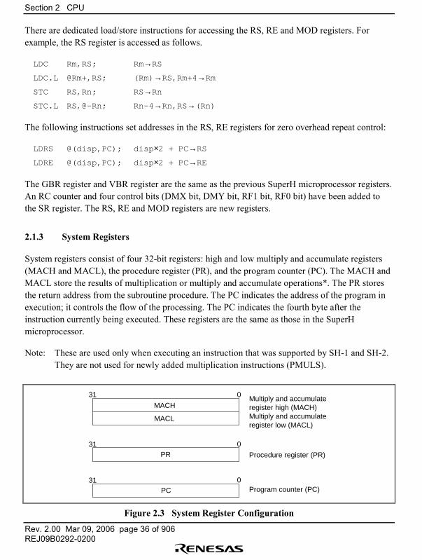
Section 2 CPU
Rev. 2.00 Mar 09, 2006 page 36 of 906REJ09B0292-0200
There are dedicated load/store instructions for accessing the RS, RE and MOD registers. Forexample, the RS register is accessed as follows.
LDC Rm,RS; Rm→RS
LDC.L @Rm+,RS; (Rm)→RS,Rm+4→Rm
STC RS,Rn; RS→Rn
STC.L RS,@-Rn; Rn-4→Rn,RS→(Rn)
The following instructions set addresses in the RS, RE registers for zero overhead repeat control:
LDRS @(disp,PC); disp×2 + PC→RS
LDRE @(disp,PC); disp×2 + PC→RE
The GBR register and VBR register are the same as the previous SuperH microprocessor registers.An RC counter and four control bits (DMX bit, DMY bit, RF1 bit, RF0 bit) have been added tothe SR register. The RS, RE and MOD registers are new registers.
2.1.3 System Registers
System registers consist of four 32-bit registers: high and low multiply and accumulate registers(MACH and MACL), the procedure register (PR), and the program counter (PC). The MACH andMACL store the results of multiplication or multiply and accumulate operations*. The PR storesthe return address from the subroutine procedure. The PC indicates the address of the program inexecution; it controls the flow of the processing. The PC indicates the fourth byte after theinstruction currently being executed. These registers are the same as those in the SuperHmicroprocessor.
Note: These are used only when executing an instruction that was supported by SH-1 and SH-2.They are not used for newly added multiplication instructions (PMULS).
MACL
PR
PC
MACH
31 0
0
0
31
31
Multiply and accumulate register high (MACH) Multiply and accumulate register low (MACL)
Procedure register (PR)
Program counter (PC)
Figure 2.3 System Register Configuration
Section 2 CPU
Rev. 2.00 Mar 09, 2006 page 37 of 906REJ09B0292-0200
In addition, among the DSP unit usage registers (DSP registers) described in 2.1.4 DSP Registers,the DSP status register (DSR) and the five registers A0, X0, X1, Y0 and Y1 of the eight dataregisters are treated as system registers. Among these, the A0 is a 40-bit register, but when data isoutput from the A0 register, the guard bit section (A0G) is disregarded; when data is input to theA0 register, the MSB of the data is copied into the guard bit section (A0G).
2.1.4 DSP Registers
The DSP unit has eight data registers and one control register as its DSP registers.
The DSP data registers are comprised of the two 40-bit registers A0 and A1, and the six 32-bitregisters M0, M1, X0, X1, Y0 and Y1. The A0 and A1 registers have the 8-bit guard bits A0G andA1G, respectively.
The DSP data registers are used for the transfer and processing of the DSP data of DSP instructionoperands. There are three types of instructions that access DSP data registers: those for DSP dataprocessing, and those for X or Y data transfer processing.
The control register is the 32-bit DSP status register (DSR) that represents operation results. TheDSR register has bits that represent operation results, a signed greater than bit (GT), a zero bit (Z),a negative value bit (N), an overflow bit (V), a DSP status bit (DC: DSP condition), and a statusselection bit (CS: condition select) for controlling DC bit setting.
The DC bit represents one status flag and is very similar to the SuperH microprocessor CPU coreT bit. For conditional DSP type instructions, DSP data processing execution is controlled inaccordance with the DC bit. This control is related to execution in the DSP unit only, and onlyDSP registers are updated. It bears no relation to address calculation or such SuperHmicroprocessor CPU core execution instructions as load/store instructions. The control bits CS(bits 2 to 0) designate the status for setting the DC bit.
DSP type instructions are comprised of unconditional DSP type instructions and conditional DSPtype instructions. The status and DC bits are updated in unconditional DSP type data processing,with the exception of the PMULS, MOVX, MOVY and MOVS instructions. Conditional DSPtype instructions are executed according to the status of the DC bit, but regardless of whether ornot they are executed, the DSR register is not updated.
Figure 2.4 shows the DSP registers. The DSR register bit functions are shown in table 2.2.Registers A0, X0, X1, Y0, Y1, and DSR are handled as system registers by CPU core instructions.
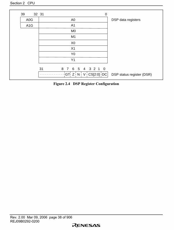
Section 2 CPU
Rev. 2.00 Mar 09, 2006 page 38 of 906REJ09B0292-0200
39 32 31 0
A0G
A1G
A0
A1
M0
M1
X0
X1
Y0
Y1
DSP data registers
DSP status register (DSR)GT Z N V CS[2:0] DC
8 7 6 5 4 3 2 1 031
Figure 2.4 DSP Register Configuration

Section 2 CPU
Rev. 2.00 Mar 09, 2006 page 39 of 906REJ09B0292-0200
Table 2.2 DSR Register Bits
Bit Name (Abbreviation) Function
31�8 Reserved bits 0: Always read out; always use 0 as a write value
7 Signed greater than bit(GT)
Indicates that the operation result is positive(excepting 0), or that operand 1 is greater thanoperand 2
1: Operation result is positive, or operand 1 is greater
6 Zero bit (Z) Indicates that the operation result is zero (0), or thatoperand 1 is equal to operand 2
1: Operation result is zero (0), or equivalence
5 Negative bit (N) Indicates that the operation result is negative, or thatoperand 1 is smaller than operand 2
1: Operation result is negative, or operand 1 issmaller
4 Overflow bit (V) Indicates that the operation result has overflowed
1: Operation result has overflowed
3�1 Status selection bits (CS) Designate the mode for selecting the operation resultstatus set in the DC bit
Do not set either 110 or 111
000: Carry/borrow mode
001: Negative value mode
010: Zero mode
011: Overflow mode
100: Signed greater mode
101: Signed above mode
0 DSP status bit (DC) Sets the status of the operation result in the modedesignated by the CS bits
0: Designated mode status not realized (unrealized)
1: Designated mode status realized
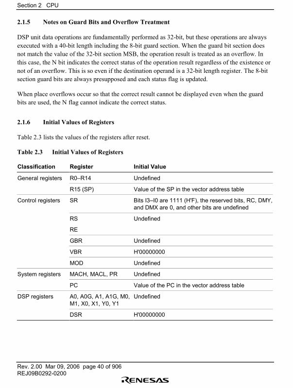
Section 2 CPU
Rev. 2.00 Mar 09, 2006 page 40 of 906REJ09B0292-0200
2.1.5 Notes on Guard Bits and Overflow Treatment
DSP unit data operations are fundamentally performed as 32-bit, but these operations are alwaysexecuted with a 40-bit length including the 8-bit guard section. When the guard bit section doesnot match the value of the 32-bit section MSB, the operation result is treated as an overflow. Inthis case, the N bit indicates the correct status of the operation result regardless of the existence ornot of an overflow. This is so even if the destination operand is a 32-bit length register. The 8-bitsection guard bits are always presupposed and each status flag is updated.
When place overflows occur so that the correct result cannot be displayed even when the guardbits are used, the N flag cannot indicate the correct status.
2.1.6 Initial Values of Registers
Table 2.3 lists the values of the registers after reset.
Table 2.3 Initial Values of Registers
Classification Register Initial Value
General registers R0�R14 Undefined
R15 (SP) Value of the SP in the vector address table
Control registers SR Bits I3�I0 are 1111 (H'F), the reserved bits, RC, DMY,and DMX are 0, and other bits are undefined
RS
RE
Undefined
GBR Undefined
VBR H'00000000
MOD Undefined
System registers MACH, MACL, PR Undefined
PC Value of the PC in the vector address table
DSP registers A0, A0G, A1, A1G, M0,M1, X0, X1, Y0, Y1
Undefined
DSR H'00000000
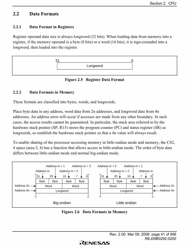
Section 2 CPU
Rev. 2.00 Mar 09, 2006 page 41 of 906REJ09B0292-0200
2.2 Data Formats
2.2.1 Data Format in Registers
Register operand data size is always longword (32 bits). When loading data from memory into aregister, if the memory operand is a byte (8 bits) or a word (16 bits), it is sign-extended into alongword, then loaded into the register.
31 0Longword
Figure 2.5 Register Data Format
2.2.2 Data Formats in Memory
These formats are classified into bytes, words, and longwords.
Place byte data in any address, word data from 2n addresses, and longword data from 4naddresses. An address error will occur if accesses are made from any other boundary. In suchcases, the access results cannot be guaranteed. In particular, the stack area referred to by thehardware stack pointer (SP, R15) stores the program counter (PC) and status register (SR) aslongwords, so establish the hardware stack pointer so that a 4n value will always result.
To enable sharing of the processor accessing memory in little-endian mode and memory, the CS2,4 space (area 2, 4) has a function that allows access in little-endian mode. The order of byte datadiffers between little-endian mode and normal big-endian mode.
31 01523 7
Byte Byte Byte Byte
WordWordAddress 2n
Address 4n Longword
Address m Address m + 2
Address m + 1 Address m + 3
Big endian
31 01523 7
Byte Byte Byte Byte
WordWord Address 2n
Address 4nLongword
Address m + 3 Address m + 1
Address m + 2 Address m
Little endian
Figure 2.6 Data Formats in Memory
Section 2 CPU
Rev. 2.00 Mar 09, 2006 page 42 of 906REJ09B0292-0200
2.2.3 Immediate Data Format
Byte immediate data is placed in an instruction code.
With the MOV, ADD, and CMP/EQ instructions, immediate data is sign-extended and operated inregisters as longword data. Immediate data accessed by the TST, AND, OR, and XOR instructionsis zero-extended and handled as longword data. Consequently, AND instructions with immediatedata always clear the upper 24 bits of the destination register.
Word or longword immediate data is not located in the instruction code; it should be placed in amemory table. Use an immediate data transfer instruction (MOV) to refer the memory table usingthe PC relative addressing mode with displacement.
2.2.4 DSP Type Data Formats
This chip has three different types of data format that correspond to various instructions. These arethe fixed-point data format, the integer data format, and the logical data format.
The DSP type fixed-point data format has a binary point fixed between bits 31 and 30. There arethree types: with guard bits, without guard bits, and multiplication input; each with different validbit lengths and value ranges.
The DSP type integer data format has a binary point fixed between bits 16 and 15. There are threetypes: with guard bits, without guard bits, and shift amount; each with different valid bit lengthsand value ranges. The shift amount of the arithmetic shift (PSHA) has a 7 bit range and canexpress values from �64 to +63, but the actual valid values are from �32 to +32. In the samemanner, the shift amount of the logical shift has a 6 bit range, but the actual valid values are from�16 to +16.
The DSP type logical data format does not have a decimal point.
The data format and valid data length are determined by the instructions and DSP registers.
Figure 2.7 shows the three DSP type data formats and binary point positions. The SuperH typedata format is also shown for reference.
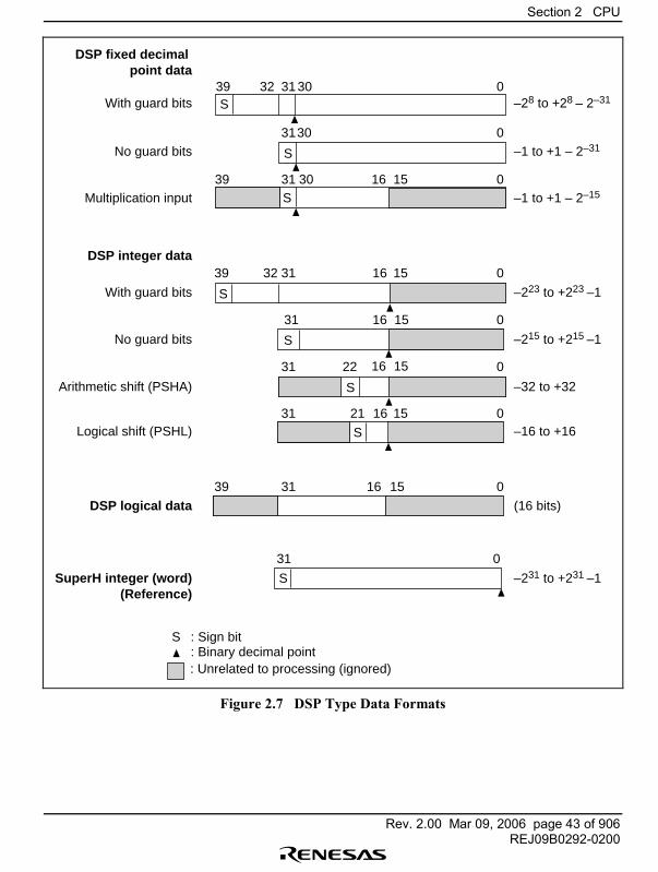
Section 2 CPU
Rev. 2.00 Mar 09, 2006 page 43 of 906REJ09B0292-0200
S
S
S
S
S
S
S
S
(16 bits)DSP logical data
SuperH integer (word)(Reference)
DSP integer data
DSP fixed decimal point data
With guard bits
No guard bits
Multiplication input
With guard bits
No guard bits
Arithmetic shift (PSHA)
Logical shift (PSHL)
39
39
39
39
32
32
31
31
31
31
31
31
31
31
31
22
21
0
0
0
0
0
0
0
0
0
–28 to +28 – 2–31
–1 to +1 – 2–31
–1 to +1 – 2–15
–223 to +223 –1
–215 to +215 –1
–32 to +32
–16 to +16
–231 to +231 –1
16 15
16
16
16
16
16
15
15
15
15
15
: Sign bitS: Binary decimal point: Unrelated to processing (ignored)
30
30
30
Figure 2.7 DSP Type Data Formats
Section 2 CPU
Rev. 2.00 Mar 09, 2006 page 44 of 906REJ09B0292-0200
2.2.5 DSP Type Instructions and Data Formats
The DSP data format and valid data length are determined by DSP type instructions and DSPregisters. There are three types of instructions that access DSP data registers, DSP data processing,X, Y data transfer processing, and single data transfer processing instructions.
DSP Data Processing: The guard bits (bits 39�32) are valid when the A0 and A1 registers areused as source registers in DSP fixed-point data processing. When any registers other than A0, A1(e.i., M0, M1, X0, X1, Y0, Y1 registers) are used as source registers, the sign-extended part of thatregister data becomes the bits 39 to 32 data. When the A0 and A1 registers are used as destinationregisters, the guard bits (bits 39�32) are valid. When any registers other than A0, A1 are used asdestination registers, bits 39 to 32 of the result data are disregarded.
Processing for DSP integer data is the same as the DSP fixed-point data processing. However, thelower word (the lower 16 bits, bits 15�0) of the source register is disregarded. The lower word ofthe destination register is cleared to 0.
In DSP logical data processing, the upper word (the upper 16 bits, bits 31�16) of the sourceregister is valid. The lower word and the guard bits of the A0, A1 registers are disregarded. Theupper word of the destination register is valid. The lower word and the guard bits of the A0, A1registers are cleared to 0.
X, Y Data Transfers: The MOVX.W and MOVY.W instructions access X, Y memory via the16-bit X, Y data buses. The data loaded into registers and data stored from registers is always theupper word (the upper 16 bits, bits 31�16).
When loading, the MOVX.W instruction loads X memory, with the X0 and X1 registers as thedestination registers. The MOVY.W instruction loads Y memory, with the Y0 and Y1 registers asthe destination registers. Data is stored in the upper word of the register; the lower word is clearedto 0.
The upper word data of the A0, A1 registers can be stored in X or Y memory with these datatransfer instructions, but storing is not possible from any other registers. The guard bits and thelower word of the A0, A1 registers are disregarded.
Single Data Transfers: The MOVS.W and MOVS.L instructions can access any memory via thedata bus (CDB). All DSP registers are connected to the CDB bus, and they can become source ordestination registers during data transfers. The two data transfer modes are word and longword.
In word mode, data is loaded to and stored in the upper word of the DSP register, with theexception of the A0G, A1G registers. In longword mode, data is loaded to and stored in the 32 bitsof the DSP register, with the exception of the A0G, A1G registers. The A0G, A1G registers can be
Section 2 CPU
Rev. 2.00 Mar 09, 2006 page 45 of 906REJ09B0292-0200
treated as independent registers during single data transfers. The load/store data length for theA0G, A1G registers is 8 bits.
If DSP registers are used as source registers in word mode, when data is stored from any registersother than A0G, A1G, the data in the upper word of the register is transferred. In the case of theA0, A1 registers, the guard bits are disregarded. When the A0G, A1G registers are the sourceregisters in word mode, only 8 bits of the data are stored from the registers; the upper bits are sign-extended.
If the DSP registers are used as destination registers in word mode, the load is to the upper word ofthe register, with the exception of A0G, A1G. When data is loaded to any register other than A0G,A1G, the lower word of the register is cleared to 0. In the case of the A0, A1 registers, the datasign is extended and stored in the guard bits; the lower word is cleared to 0. When the A0G, A1Gregisters are the destination registers in word mode, the least significant 8 bits of the data areloaded into the registers; the A0, A1 registers are not zero cleared but retain their previous values.
If the DSP registers are used as source registers in longword mode, when data is stored from anyregisters other than A0G, A1G, the 32 bits (data) of the register are transferred. When the A0, A1registers are used as the source registers the guard bits are disregarded. When the A0G, A1Gregisters are the source registers in longword mode, only 8 bits of the data are stored from theregisters; the upper bits are sign-extended.
If the DSP registers are used as destination registers in longword mode, the load is to the 32 bits ofthe register, with the exception of A0G, A1G. In the case of the A0, A1 registers, the data sign isextended and stored in the guard bits. When the A0G, A1G registers are the destination registers inlongword mode, the least significant 8 bits of the data are loaded into the registers; the A0, A1registers are not zero cleared but retain their previous values.
Tables 2.4 and 2.5 indicate the register data formats for DSP instructions. Some registers cannotbe accessed by certain instructions. For example, the PMULS instruction can designate the A1register as a source register but cannot designate A0 as such. Refer to the instruction explanationsfor details.
Figure 2.8 shows the relationship between the buses and the DSP registers during transfers.
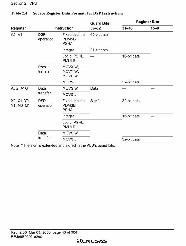
Section 2 CPU
Rev. 2.00 Mar 09, 2006 page 46 of 906REJ09B0292-0200
Table 2.4 Source Register Data Formats for DSP Instructions
Guard Bits Register Bits
Register Instruction 39�32 31�16 15�0
A0, A1 DSPoperation
Fixed decimal,PDMSB,PSHA
40-bit data
Integer 24-bit data �
Logic, PSHL,PMULS
� 16-bit data
Datatransfer
MOVX.W,MOVY.W,MOVS.W
MOVS.L 32-bit data
A0G, A1G Data MOVS.W Data � �transfer MOVS.L
X0, X1, Y0,Y1, M0, M1
DSPoperation
Fixed decimal,PDMSB,PSHA
Sign* 32-bit data
Integer 16-bit data �
Logic, PSHL,PMULS
�
Data MOVS.Wtransfer MOVS.L 32-bit data
Note: * The sign is extended and stored in the ALU�s guard bits.
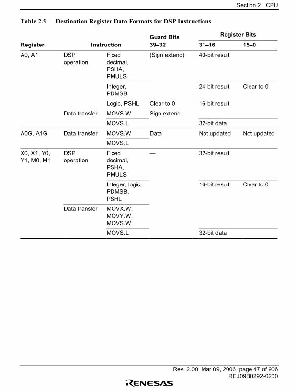
Section 2 CPU
Rev. 2.00 Mar 09, 2006 page 47 of 906REJ09B0292-0200
Table 2.5 Destination Register Data Formats for DSP Instructions
Guard Bits Register Bits
Register Instruction 39�32 31�16 15�0
A0, A1 DSPoperation
Fixeddecimal,PSHA,PMULS
(Sign extend) 40-bit result
Integer,PDMSB
24-bit result Clear to 0
Logic, PSHL Clear to 0 16-bit result
Data transfer MOVS.W Sign extend
MOVS.L 32-bit data
A0G, A1G Data transfer MOVS.W Data Not updated Not updated
MOVS.L
X0, X1, Y0,Y1, M0, M1
DSPoperation
Fixeddecimal,PSHA,PMULS
� 32-bit result
Integer, logic,PDMSB,PSHL
16-bit result Clear to 0
Data transfer MOVX.W,MOVY.W,MOVS.W
MOVS.L 32-bit data

Section 2 CPU
Rev. 2.00 Mar 09, 2006 page 48 of 906REJ09B0292-0200
39 32
31
0
A0G
A1G
A0
A1
M0
M1
X0
X1
Y0
Y1
DSR
CDB
XDB
YDB
MOVS.W,MOVS.L
32 bits16 bits
16 bits
16 bits
32 bits
MOVX.W,MOVY.WMOVS.W,
MOVS.L
16
8 bits
7 0
[7:0]
Figure 2.8 DSP Register-Bus Relationship during Data Transfers
2.3 CPU Core Instruction Features
The CPU core instructions are RISC type. The characteristics are as follows.
16-Bit Fixed Length: All instructions are 16 bits long, increasing program code efficiency.
One Instruction per Cycle: The microprocessor can execute basic instructions in one cycle usingthe pipeline system. One state equals 16.0 ns when operating at 62.5 MHz.
Data Length: Longword is the basic data length for all operations. Memory can be accessed inbytes, words, or longwords. Byte or word data accessed from memory is sign-extended andhandled as longword data. Immediate data is sign-extended for arithmetic operations or zero-extended for logic operations. It also is handled as longword data.
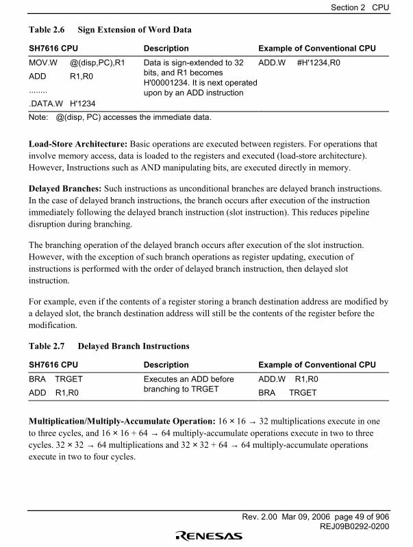
Section 2 CPU
Rev. 2.00 Mar 09, 2006 page 49 of 906REJ09B0292-0200
Table 2.6 Sign Extension of Word Data
SH7616 CPU Description Example of Conventional CPU
MOV.W @(disp,PC),R1
ADD R1,R0
........
.DATA.W H'1234
Data is sign-extended to 32bits, and R1 becomesH'00001234. It is next operatedupon by an ADD instruction
ADD.W #H'1234,R0
Note: @(disp, PC) accesses the immediate data.
Load-Store Architecture: Basic operations are executed between registers. For operations thatinvolve memory access, data is loaded to the registers and executed (load-store architecture).However, Instructions such as AND manipulating bits, are executed directly in memory.
Delayed Branches: Such instructions as unconditional branches are delayed branch instructions.In the case of delayed branch instructions, the branch occurs after execution of the instructionimmediately following the delayed branch instruction (slot instruction). This reduces pipelinedisruption during branching.
The branching operation of the delayed branch occurs after execution of the slot instruction.However, with the exception of such branch operations as register updating, execution ofinstructions is performed with the order of delayed branch instruction, then delayed slotinstruction.
For example, even if the contents of a register storing a branch destination address are modified bya delayed slot, the branch destination address will still be the contents of the register before themodification.
Table 2.7 Delayed Branch Instructions
SH7616 CPU Description Example of Conventional CPU
BRA TRGET
ADD R1,R0
Executes an ADD beforebranching to TRGET
ADD.W R1,R0
BRA TRGET
Multiplication/Multiply-Accumulate Operation: 16 × 16 → 32 multiplications execute in oneto three cycles, and 16 × 16 + 64 → 64 multiply-accumulate operations execute in two to threecycles. 32 × 32 → 64 multiplications and 32 × 32 + 64 → 64 multiply-accumulate operationsexecute in two to four cycles.
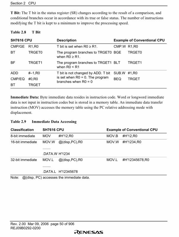
Section 2 CPU
Rev. 2.00 Mar 09, 2006 page 50 of 906REJ09B0292-0200
T Bit: The T bit in the status register (SR) changes according to the result of a comparison, andconditional branches occur in accordance with its true or false status. The number of instructionsmodifying the T bit is kept to a minimum to improve the processing speed.
Table 2.8 T Bit
SH7616 CPU Description Example of Conventional CPU
CMP/GE R1,R0
BT TRGET0
BF TRGET1
T bit is set when R0 ≥ R1.
The program branches to TRGET0when R0 ≥ R1.
The program branches to TRGET1when R0 < R1
CMP.W R1,R0
BGE TRGET0
BLT TRGET1
ADD #�1,R0
CMP/EQ #0,R0
BT TRGET
T bit is not changed by ADD. T bitis set when R0 = 0. The programbranches when R0 = 0
SUB.W #1,R0
BEQ TRGET
Immediate Data: Byte immediate data resides in instruction code. Word or longword immediatedata is not input in instruction codes but is stored in a memory table. An immediate data transferinstruction (MOV) accesses the memory table using the PC relative addressing mode withdisplacement.
Table 2.9 Immediate Data Accessing
Classification SH7616 CPU Example of Conventional CPU
8-bit immediate MOV #H'12,R0 MOV.B #H'12,R0
16-bit immediate MOV.W @(disp,PC),R0
........
.DATA.W H'1234
MOV.W #H'1234,R0
32-bit immediate MOV.L @(disp,PC),R0
........
.DATA.L H'12345678
MOV.L #H'12345678,R0
Note: @(disp, PC) accesses the immediate data.
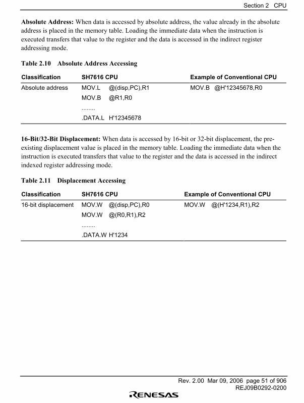
Section 2 CPU
Rev. 2.00 Mar 09, 2006 page 51 of 906REJ09B0292-0200
Absolute Address: When data is accessed by absolute address, the value already in the absoluteaddress is placed in the memory table. Loading the immediate data when the instruction isexecuted transfers that value to the register and the data is accessed in the indirect registeraddressing mode.
Table 2.10 Absolute Address Accessing
Classification SH7616 CPU Example of Conventional CPU
Absolute address MOV.L @(disp,PC),R1
MOV.B @R1,R0
........
.DATA.L H'12345678
MOV.B @H'12345678,R0
16-Bit/32-Bit Displacement: When data is accessed by 16-bit or 32-bit displacement, the pre-existing displacement value is placed in the memory table. Loading the immediate data when theinstruction is executed transfers that value to the register and the data is accessed in the indirectindexed register addressing mode.
Table 2.11 Displacement Accessing
Classification SH7616 CPU Example of Conventional CPU
16-bit displacement MOV.W @(disp,PC),R0
MOV.W @(R0,R1),R2
........
.DATA.W H'1234
MOV.W @(H'1234,R1),R2
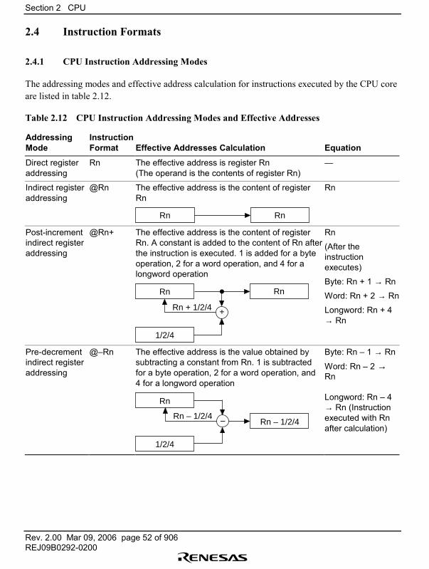
Section 2 CPU
Rev. 2.00 Mar 09, 2006 page 52 of 906REJ09B0292-0200
2.4 Instruction Formats
2.4.1 CPU Instruction Addressing Modes
The addressing modes and effective address calculation for instructions executed by the CPU coreare listed in table 2.12.
Table 2.12 CPU Instruction Addressing Modes and Effective Addresses
AddressingMode
InstructionFormat Effective Addresses Calculation Equation
Direct registeraddressing
Rn The effective address is register Rn(The operand is the contents of register Rn)
�
Indirect registeraddressing
@Rn The effective address is the content of registerRn
Rn Rn
Rn
Post-incrementindirect registeraddressing
@Rn+ The effective address is the content of registerRn. A constant is added to the content of Rn afterthe instruction is executed. 1 is added for a byteoperation, 2 for a word operation, and 4 for alongword operation
Rn Rn
1/2/4
+Rn + 1/2/4
Rn
(After theinstructionexecutes)
Byte: Rn + 1 → Rn
Word: Rn + 2 → Rn
Longword: Rn + 4→ Rn
Pre-decrementindirect registeraddressing
@�Rn The effective address is the value obtained bysubtracting a constant from Rn. 1 is subtractedfor a byte operation, 2 for a word operation, and4 for a longword operation
Rn
1/2/4
Rn – 1/2/4–Rn – 1/2/4
Byte: Rn � 1 → Rn
Word: Rn � 2 →Rn
Longword: Rn � 4→ Rn (Instructionexecuted with Rnafter calculation)
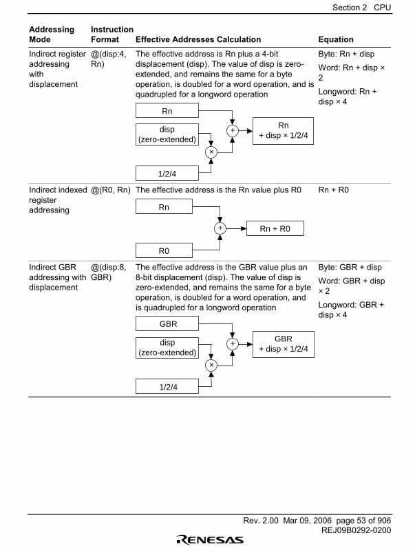
Section 2 CPU
Rev. 2.00 Mar 09, 2006 page 53 of 906REJ09B0292-0200
AddressingMode
InstructionFormat Effective Addresses Calculation Equation
Indirect registeraddressingwithdisplacement
@(disp:4,Rn)
The effective address is Rn plus a 4-bitdisplacement (disp). The value of disp is zero-extended, and remains the same for a byteoperation, is doubled for a word operation, and isquadrupled for a longword operation
Rn
1/2/4
+
×
disp(zero-extended)
Rn+ disp × 1/2/4
Byte: Rn + disp
Word: Rn + disp ×2
Longword: Rn +disp × 4
Indirect indexedregisteraddressing
@(R0, Rn) The effective address is the Rn value plus R0
Rn
R0
Rn + R0+
Rn + R0
Indirect GBRaddressing withdisplacement
@(disp:8,GBR)
The effective address is the GBR value plus an8-bit displacement (disp). The value of disp iszero-extended, and remains the same for a byteoperation, is doubled for a word operation, andis quadrupled for a longword operation
GBR
1/2/4
+
×
disp(zero-extended)
GBR+ disp × 1/2/4
Byte: GBR + disp
Word: GBR + disp× 2
Longword: GBR +disp × 4
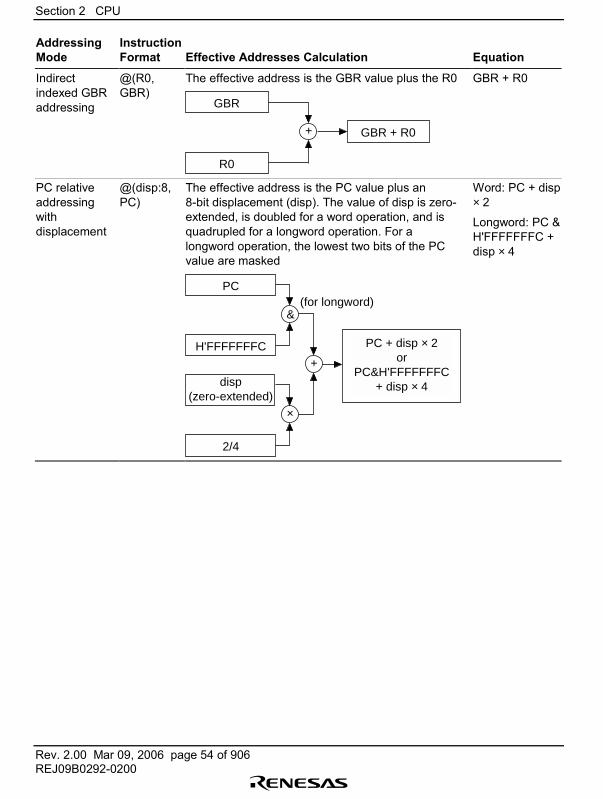
Section 2 CPU
Rev. 2.00 Mar 09, 2006 page 54 of 906REJ09B0292-0200
AddressingMode
InstructionFormat Effective Addresses Calculation Equation
Indirectindexed GBRaddressing
@(R0,GBR)
The effective address is the GBR value plus the R0
GBR
R0
GBR + R0+
GBR + R0
PC relativeaddressingwithdisplacement
@(disp:8,PC)
The effective address is the PC value plus an8-bit displacement (disp). The value of disp is zero-extended, is doubled for a word operation, and isquadrupled for a longword operation. For alongword operation, the lowest two bits of the PCvalue are masked
PC
H'FFFFFFFC+
2/4
×
&(for longword)
disp(zero-extended)
PC + disp × 2or
PC&H'FFFFFFFC+ disp × 4
Word: PC + disp× 2
Longword: PC &H'FFFFFFFC +disp × 4
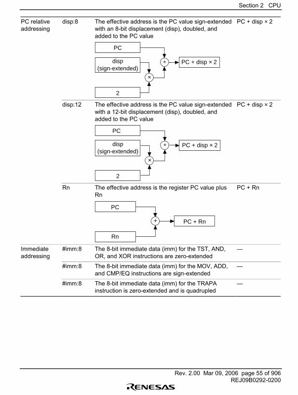
Section 2 CPU
Rev. 2.00 Mar 09, 2006 page 55 of 906REJ09B0292-0200
PC relativeaddressing
disp:8 The effective address is the PC value sign-extendedwith an 8-bit displacement (disp), doubled, andadded to the PC value
PC
2
+
×
disp(sign-extended)
PC + disp × 2
PC + disp × 2
disp:12 The effective address is the PC value sign-extendedwith a 12-bit displacement (disp), doubled, andadded to the PC value
PC
2
+
×
disp(sign-extended)
PC + disp × 2
PC + disp × 2
Rn The effective address is the register PC value plusRn
PC
Rn
+ PC + Rn
PC + Rn
Immediateaddressing
#imm:8 The 8-bit immediate data (imm) for the TST, AND,OR, and XOR instructions are zero-extended
�
#imm:8 The 8-bit immediate data (imm) for the MOV, ADD,and CMP/EQ instructions are sign-extended
�
#imm:8 The 8-bit immediate data (imm) for the TRAPAinstruction is zero-extended and is quadrupled
�
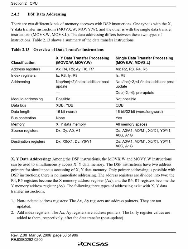
Section 2 CPU
Rev. 2.00 Mar 09, 2006 page 56 of 906REJ09B0292-0200
2.4.2 DSP Data Addressing
There are two different kinds of memory accesses with DSP instructions. One type is with the X,Y data transfer instructions (MOVX.W, MOVY.W), and the other is with the single data transferinstructions (MOVS.W, MOVS.L). The data addressing differs between these two types ofinstructions. Table 2.13 shows a summary of the data transfer instructions.
Table 2.13 Overview of Data Transfer Instructions
ClassificationX, Y Data Transfer Processing(MOVX.W, MOVY.W)
Single Data Transfer Processing(MOVS.W, MOVS.L)
Address registers Ax: R4, R5; Ay: R6, R7 As: R2, R3, R4, R5
Index registers Ix: R8, Iy: R9 Is: R8
Addressing Nop/Inc(+2)/index addition: post-update
Nop/Inc(+2,+4)/index addition: post-update
� Dec(�2,�4): pre-update
Modulo addressing Possible Not possible
Data bus XDB, YDB CDB
Data length 16 bit (word) 16 bit/32 bit (word/longword)
Bus contention None Yes
Memory X, Y data memory All memory spaces
Source registers Dx, Dy: A0, A1 Ds: A0/A1, M0/M1, X0/X1, Y0/Y1,A0G, A1G
Destination registers Dx: X0/X1; Dy: Y0/Y1 Ds: A0/A1, M0/M1, X0/X1, Y0/Y1,A0G, A1G
X, Y Data Addressing: Among the DSP instructions, the MOVX.W and MOVY.W instructionscan be used to simultaneously access X, Y data memory. The DSP instructions have two addresspointers for simultaneous accessing of X, Y data memory. Only pointer addressing is possible withDSP instructions; there is no immediate addressing. The address registers are divided into two; theR4, R5 registers become the X memory address register (Ax), and the R6, R7 registers become theY memory address register (Ay). The following three types of addressing exist with X, Y datatransfer instructions.
1. Non-updated address registers: The Ax, Ay registers are address pointers. They are notupdated.
2. Add index registers: The Ax, Ay registers are address pointers. The Ix, Iy register values areadded to them, respectively, after the data transfer (post-update).
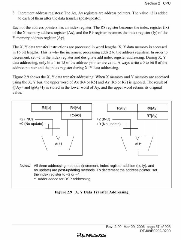
Section 2 CPU
Rev. 2.00 Mar 09, 2006 page 57 of 906REJ09B0292-0200
3. Increment address registers: The Ax, Ay registers are address pointers. The value +2 is addedto each of them after the data transfer (post-update).
Each of the address pointers has an index register. The R8 register becomes the index register (Ix)of the X memory address register (Ax), and the R9 register becomes the index register (Iy) of theY memory address register (Ay).
The X, Y data transfer instructions are processed in word lengths. X, Y data memory is accessedin 16 bit lengths. This is why the increment processing adds 2 to the address registers. In order todecrement, set �2 in the index register and designate add index register addressing. During X, Ydata addressing, only bits 1 to 15 of the address pointer are valid. Always write a 0 to bit 0 of theaddress pointer and the index register during X, Y data addressing.
Figure 2.9 shows the X, Y data transfer addressing. When X memory and Y memory are accessedusing the X, Y bus, the upper word of Ax (R4 or R5) and Ay (R6 or R7) is ignored. The result of@Ay+ and @Ay+Iy is stored in the lower word of Ay, and the upper word retains its originalvalue.
ALU AU*
R8[Ix] R4[Ax]
R5[Ax]
R9[Iy] R6[Ay]
R7[Ay]+2 (INC) +2 (INC)+0 (No update) +0 (No update)
Notes: All three addressing methods (increment, index register addition (Ix, Iy), and no update) are post-updating methods. To decrement the address pointer, set the index register to –2 or –4.* Adder added for DSP addressing.
Figure 2.9 X, Y Data Transfer Addressing
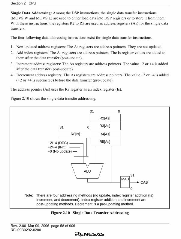
Section 2 CPU
Rev. 2.00 Mar 09, 2006 page 58 of 906REJ09B0292-0200
Single Data Addressing: Among the DSP instructions, the single data transfer instructions(MOVS.W and MOVS.L) are used to either load data into DSP registers or to store it from them.With these instructions, the registers R2 to R5 are used as address registers (As) for the single datatransfers.
The four following data addressing instructions exist for single data transfer instructions.
1. Non-updated address registers: The As registers are address pointers. They are not updated.2. Add index registers: The As registers are address pointers. The Is register values are added to
them after the data transfer (post-update).3. Increment address registers: The As registers are address pointers. The value +2 or +4 is added
after the data transfer (post-update).4. Decrement address registers: The As registers are address pointers. The value �2 or �4 is added
(+2 or +4 is subtracted) before the data transfer (pre-update).
The address pointer (As) uses the R8 register as an index register (Is).
Figure 2.10 shows the single data transfer addressing.
ALU
R8[Is] R4[As]
R5[As]
+2/+4 (INC)+0 (No update)
Note: There are four addressing methods (no update, index register addition (Is), increment, and decrement). Index register addition and increment are post-updating methods. Decrement is a pre-updating method.
R3[As]
R2[As]
–2/–4 (DEC)
31
31 0
31
0
0
MABCAB
Figure 2.10 Single Data Transfer Addressing
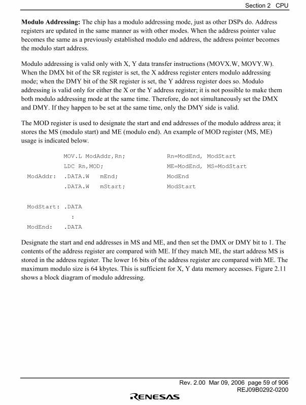
Section 2 CPU
Rev. 2.00 Mar 09, 2006 page 59 of 906REJ09B0292-0200
Modulo Addressing: The chip has a modulo addressing mode, just as other DSPs do. Addressregisters are updated in the same manner as with other modes. When the address pointer valuebecomes the same as a previously established modulo end address, the address pointer becomesthe modulo start address.
Modulo addressing is valid only with X, Y data transfer instructions (MOVX.W, MOVY.W).When the DMX bit of the SR register is set, the X address register enters modulo addressingmode; when the DMY bit of the SR register is set, the Y address register does so. Moduloaddressing is valid only for either the X or the Y address register; it is not possible to make themboth modulo addressing mode at the same time. Therefore, do not simultaneously set the DMXand DMY. If they happen to be set at the same time, only the DMY side is valid.
The MOD register is used to designate the start and end addresses of the modulo address area; itstores the MS (modulo start) and ME (modulo end). An example of MOD register (MS, ME)usage is indicated below.
MOV.L ModAddr,Rn; Rn=ModEnd, ModStart
LDC Rn,MOD; ME=ModEnd, MS=ModStart
ModAddr: .DATA.W mEnd; ModEnd
.DATA.W mStart; ModStart
ModStart: .DATA
:
ModEnd: .DATA
Designate the start and end addresses in MS and ME, and then set the DMX or DMY bit to 1. Thecontents of the address register are compared with ME. If they match ME, the start address MS isstored in the address register. The lower 16 bits of the address register are compared with ME. Themaximum modulo size is 64 kbytes. This is sufficient for X, Y data memory accesses. Figure 2.11shows a block diagram of modulo addressing.
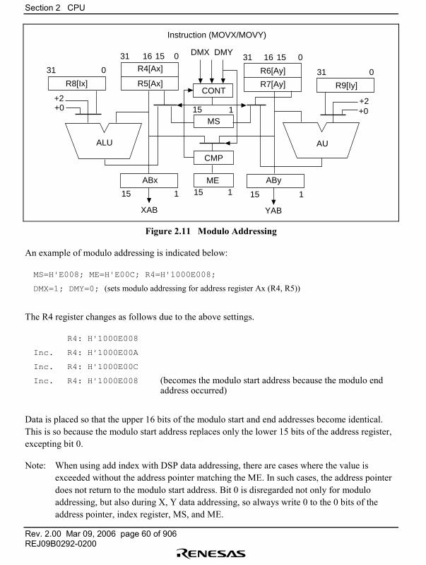
Section 2 CPU
Rev. 2.00 Mar 09, 2006 page 60 of 906REJ09B0292-0200
Instruction (MOVX/MOVY)
DMX
CONT
MS
CMP
ME
ALU AU
ABx ABy
R4[Ax] R6[Ay]
R5[Ax] R7[Ay]R8[Ix] R9[Iy]
DMY
31 0
0 0
0
1
1
16 16
15 15 15
31 31
31
+2+0
+2+0
15 15
1 1
XAB YAB
15
Figure 2.11 Modulo Addressing
An example of modulo addressing is indicated below:
MS=H'E008; ME=H'E00C; R4=H'1000E008;
DMX=1; DMY=0; (sets modulo addressing for address register Ax (R4, R5))
The R4 register changes as follows due to the above settings.
R4: H'1000E008
Inc. R4: H'1000E00A
Inc. R4: H'1000E00C
Inc. R4: H'1000E008 (becomes the modulo start address because the modulo end address occurred)
Data is placed so that the upper 16 bits of the modulo start and end addresses become identical.This is so because the modulo start address replaces only the lower 15 bits of the address register,excepting bit 0.
Note: When using add index with DSP data addressing, there are cases where the value isexceeded without the address pointer matching the ME. In such cases, the address pointerdoes not return to the modulo start address. Bit 0 is disregarded not only for moduloaddressing, but also during X, Y data addressing, so always write 0 to the 0 bits of theaddress pointer, index register, MS, and ME.
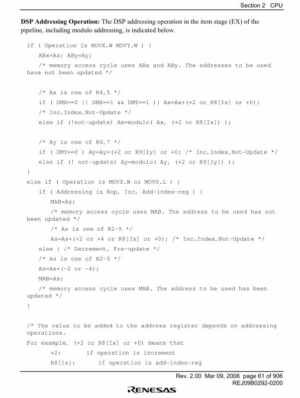
Section 2 CPU
Rev. 2.00 Mar 09, 2006 page 61 of 906REJ09B0292-0200
DSP Addressing Operation: The DSP addressing operation in the item stage (EX) of thepipeline, including modulo addressing, is indicated below.
if ( Operation is MOVX.W MOVY.W ) {
ABx=Ax; ABy=Ay;
/* memory access cycle uses ABx and ABy. The addresses to be usedhave not been updated */
/* Ax is one of R4,5 */
if ( DMX==0 || DMX==1 && DMY==1 )} Ax=Ax+(+2 or R8[Ix} or +0);
/* Inc,Index,Not-Update */
else if (!not-update) Ax=modulo( Ax, (+2 or R8[Ix]) );
/* Ay is one of R6,7 */
if ( DMY==0 ) Ay=Ay+(+2 or R9[Iy] or +0; /* Inc,Index,Not-Update */
else if (! not-update) Ay=modulo( Ay, (+2 or R9[Iy]) );
}
else if ( Operation is MOVS.W or MOVS.L ) {
if ( Addressing is Nop, Inc, Add-index-reg ) {
MAB=As;
/* memory access cycle uses MAB. The address to be used has notbeen updated */
/* As is one of R2–5 */
As=As+(+2 or +4 or R8[Is] or +0); /* Inc.Index,Not-Update */
else { /* Decrement, Pre-update */
/* As is one of R2–5 */
As=As+(–2 or –4);
MAB=As;
/* memory access cycle uses MAB. The address to be used has beenupdated */
}
/* The value to be added to the address register depends on addressingoperations.
For example, (+2 or R8[Ix] or +0) means that
+2: if operation is increment
R8[Ix}: if operation is add-index-reg
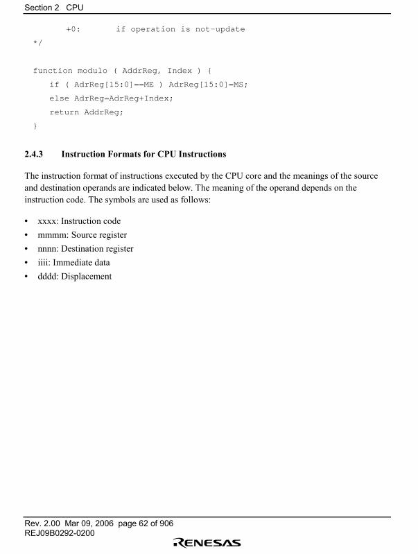
Section 2 CPU
Rev. 2.00 Mar 09, 2006 page 62 of 906REJ09B0292-0200
+0: if operation is not-update
*/
function modulo ( AddrReg, Index ) {
if ( AdrReg[15:0]==ME ) AdrReg[15:0]=MS;
else AdrReg=AdrReg+Index;
return AddrReg;
}
2.4.3 Instruction Formats for CPU Instructions
The instruction format of instructions executed by the CPU core and the meanings of the sourceand destination operands are indicated below. The meaning of the operand depends on theinstruction code. The symbols are used as follows:
• xxxx: Instruction code• mmmm: Source register• nnnn: Destination register• iiii: Immediate data• dddd: Displacement
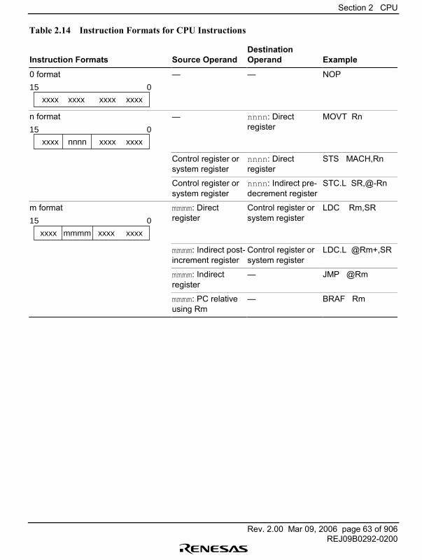
Section 2 CPU
Rev. 2.00 Mar 09, 2006 page 63 of 906REJ09B0292-0200
Table 2.14 Instruction Formats for CPU Instructions
Instruction Formats Source OperandDestinationOperand Example
0 format
xxxx xxxx xxxxxxxx
15 0
� � NOP
n format
xxxx xxxx xxxxnnnn
15 0
� nnnn: Directregister
MOVT Rn
Control register orsystem register
nnnn: Directregister
STS MACH,Rn
Control register orsystem register
nnnn: Indirect pre-decrement register
STC.L SR,@-Rn
m format
xxxxmmmmxxxx xxxx
15 0
mmmm: Directregister
Control register orsystem register
LDC Rm,SR
mmmm: Indirect post-increment register
Control register orsystem register
LDC.L @Rm+,SR
mmmm: Indirectregister
� JMP @Rm
mmmm: PC relativeusing Rm
� BRAF Rm
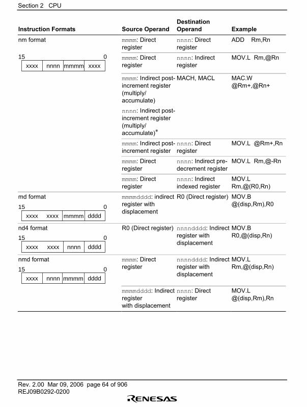
Section 2 CPU
Rev. 2.00 Mar 09, 2006 page 64 of 906REJ09B0292-0200
Instruction Formats Source OperandDestinationOperand Example
nm format mmmm: Directregister
nnnn: Directregister
ADD Rm,Rn
nnnnxxxx xxxx
15 0
mmmmmmmm: Directregister
nnnn: Indirectregister
MOV.L Rm,@Rn
mmmm: Indirect post-increment register(multiply/accumulate)
nnnn: Indirect post-increment register(multiply/accumulate)*
MACH, MACL MAC.W@Rm+,@Rn+
mmmm: Indirect post-increment register
nnnn: Directregister
MOV.L @Rm+,Rn
mmmm: Directregister
nnnn: Indirect pre-decrement register
MOV.L Rm,@-Rn
mmmm: Directregister
nnnn: Indirectindexed register
MOV.LRm,@(R0,Rn)
md format
xxxx dddd
15 0
mmmmxxxx
mmmmdddd: indirectregister withdisplacement
R0 (Direct register) MOV.B@(disp,Rm),R0
nd4 format
ddddnnnnxxxx
15 0
xxxx
R0 (Direct register) nnnndddd: Indirectregister withdisplacement
MOV.BR0,@(disp,Rn)
nmd format
nnnnxxxx dddd
15 0
mmmm
mmmm: Directregister
nnnndddd: Indirectregister withdisplacement
MOV.LRm,@(disp,Rn)
mmmmdddd: Indirectregisterwith displacement
nnnn: Directregister
MOV.L@(disp,Rm),Rn

Section 2 CPU
Rev. 2.00 Mar 09, 2006 page 65 of 906REJ09B0292-0200
Instruction Formats Source OperandDestinationOperand Example
d format
ddddxxxx
15 0
xxxx dddd
dddddddd: IndirectGBR withdisplacement
R0 (Direct register) MOV.L@(disp,GBR),R0
R0(Direct register) dddddddd: IndirectGBR withdisplacement
MOV.LR0,@(disp,GBR)
dddddddd: PCrelative withdisplacement
R0 (Direct register) MOVA@(disp,PC),R0
dddddddd: PCrelative
� BF label
d12 format
ddddxxxx
15 0
dddd dddd
dddddddddddd:PC relative
� BRA label
(label=disp+PC)
nd8 format
ddddnnnnxxxx
15 0
dddd
dddddddd: PCrelative withdisplacement
nnnn: Directregister
MOV.L@(disp,PC),Rn
i format iiiiiiii:Immediate
Indirect indexedGBR
AND.B#imm,@(R0,GBR)
i i i ixxxx
15 0
xxxx i i i i
iiiiiiii:Immediate
R0 (Direct register) AND #imm,R0
iiiiiiii:Immediate
� TRAPA #imm
ni format
nnnn i i i ixxxx
15 0
i i i i
iiiiiiii:Immediate
nnnn: Directregister
ADD #imm,Rn
Note: * In multiply/accumulate instructions, nnnn is the source register.
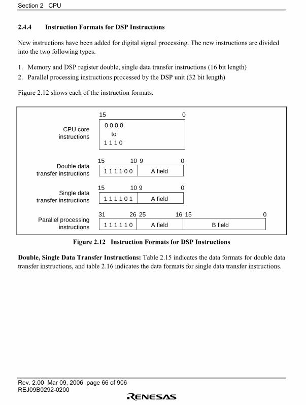
Section 2 CPU
Rev. 2.00 Mar 09, 2006 page 66 of 906REJ09B0292-0200
2.4.4 Instruction Formats for DSP Instructions
New instructions have been added for digital signal processing. The new instructions are dividedinto the two following types.
1. Memory and DSP register double, single data transfer instructions (16 bit length)2. Parallel processing instructions processed by the DSP unit (32 bit length)
Figure 2.12 shows each of the instruction formats.
CPU coreinstructions
0 0 0 0to
1 1 1 0
Double datatransfer instructions
Single datatransfer instructions
Parallel processinginstructions B field
A field
A field
A field
1 1 1 1 0 0
1 1 1 1 0 1
1 1 1 1 1 0
15
15
15
15
0
0
0
031
10
10
9
9
1626 25
Figure 2.12 Instruction Formats for DSP Instructions
Double, Single Data Transfer Instructions: Table 2.15 indicates the data formats for double datatransfer instructions, and table 2.16 indicates the data formats for single data transfer instructions.
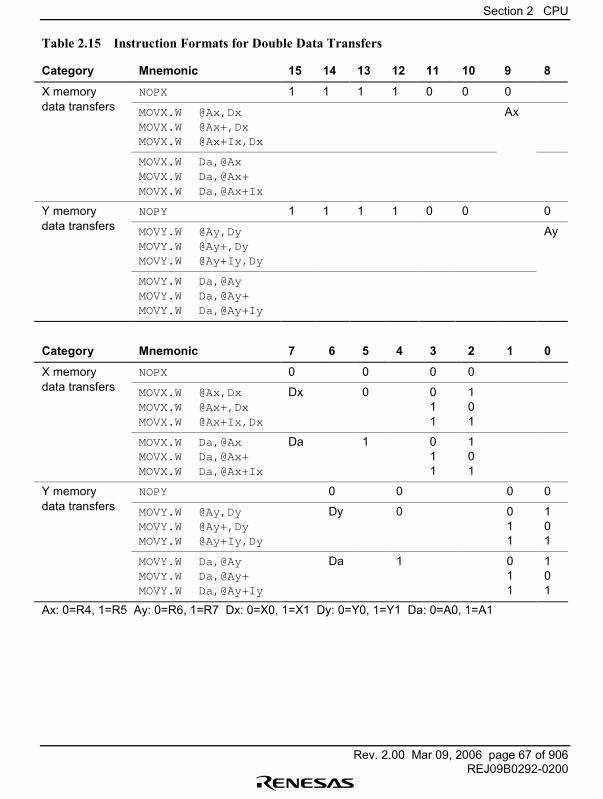
Section 2 CPU
Rev. 2.00 Mar 09, 2006 page 67 of 906REJ09B0292-0200
Table 2.15 Instruction Formats for Double Data Transfers
Category Mnemonic 15 14 13 12 11 10 9 8
X memory NOPX 1 1 1 1 0 0 0data transfers MOVX.W @Ax,Dx
MOVX.W @Ax+,DxMOVX.W @Ax+Ix,Dx
Ax
MOVX.W Da,@AxMOVX.W Da,@Ax+MOVX.W Da,@Ax+Ix
Y memory NOPY 1 1 1 1 0 0 0data transfers MOVY.W @Ay,Dy
MOVY.W @Ay+,DyMOVY.W @Ay+Iy,Dy
Ay
MOVY.W Da,@AyMOVY.W Da,@Ay+MOVY.W Da,@Ay+Iy
Category Mnemonic 7 6 5 4 3 2 1 0
X memory NOPX 0 0 0 0data transfers MOVX.W @Ax,Dx
MOVX.W @Ax+,DxMOVX.W @Ax+Ix,Dx
Dx 0 011
101
MOVX.W Da,@AxMOVX.W Da,@Ax+MOVX.W Da,@Ax+Ix
Da 1 011
101
Y memory NOPY 0 0 0 0data transfers MOVY.W @Ay,Dy
MOVY.W @Ay+,DyMOVY.W @Ay+Iy,Dy
Dy 0 011
101
MOVY.W Da,@AyMOVY.W Da,@Ay+MOVY.W Da,@Ay+Iy
Da 1 011
101
Ax: 0=R4, 1=R5 Ay: 0=R6, 1=R7 Dx: 0=X0, 1=X1 Dy: 0=Y0, 1=Y1 Da: 0=A0, 1=A1
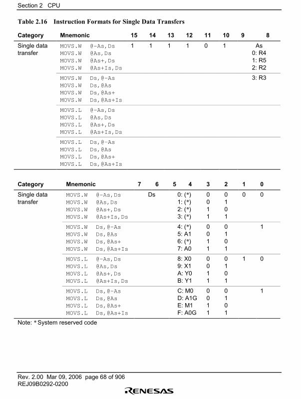
Section 2 CPU
Rev. 2.00 Mar 09, 2006 page 68 of 906REJ09B0292-0200
Table 2.16 Instruction Formats for Single Data Transfers
Category Mnemonic 15 14 13 12 11 10 9 8
Single datatransfer
MOVS.W @–As,DsMOVS.W @As,DsMOVS.W @As+,DsMOVS.W @As+Is,Ds
1 1 1 1 0 1 As0: R41: R52: R2
MOVS.W Ds,@-AsMOVS.W Ds,@AsMOVS.W Ds,@As+MOVS.W Ds,@As+Is
3: R3
MOVS.L @–As,DsMOVS.L @As,DsMOVS.L @As+,DsMOVS.L @As+Is,Ds
MOVS.L Ds,@-AsMOVS.L Ds,@AsMOVS.L Ds,@As+MOVS.L Ds,@As+Is
Category Mnemonic 7 6 5 4 3 2 1 0
Single datatransfer
MOVS.W @–As,DsMOVS.W @As,DsMOVS.W @As+,DsMOVS.W @As+Is,Ds
Ds 0: (*)1: (*)2: (*)3: (*)
0011
0101
0 0
MOVS.W Ds,@-AsMOVS.W Ds,@AsMOVS.W Ds,@As+MOVS.W Ds,@As+Is
4: (*)5: A16: (*)7: A0
0011
0101
1
MOVS.L @–As,DsMOVS.L @As,DsMOVS.L @As+,DsMOVS.L @As+Is,Ds
8: X09: X1A: Y0B: Y1
0011
0101
1 0
MOVS.L Ds,@-AsMOVS.L Ds,@AsMOVS.L Ds,@As+MOVS.L Ds,@As+Is
C: M0D: A1GE: M1F: A0G
0011
0101
1
Note: * System reserved code
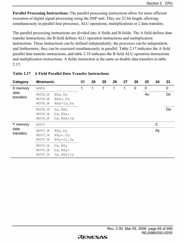
Section 2 CPU
Rev. 2.00 Mar 09, 2006 page 69 of 906REJ09B0292-0200
Parallel Processing Instructions: The parallel processing instructions allow for more efficientexecution of digital signal processing using the DSP unit. They are 32 bit length, allowingsimultaneously in parallel four processes, ALU operations, multiplications or 2 data transfers.
The parallel processing instructions are divided into A fields and B fields. The A field defines datatransfer instructions; the B field defines ALU operation instructions and multiplicationinstructions. These instructions can be defined independently, the processes can be independent,and furthermore, they can be executed simultaneously in parallel. Table 2.17 indicates the A fieldparallel data transfer instructions, and table 2.18 indicates the B field ALU operation instructionsand multiplication instructions. A fields instruction is the same as double data transfers in table2.15.
Table 2.17 A Field Parallel Data Transfer Instructions
Category Mnemonic 31 30 29 28 27 26 25 24 23
X memory NOPX 1 1 1 1 1 0 0 0datatransfers
MOVX.W @Ax,DxMOVX.W @Ax+,DxMOVX.W @Ax+Ix,Dx
Ax Dx
MOVX.W Da,@AxMOVX.W Da,@Ax+MOVX.W Da,@Ax+Ix
Da
Y memory NOPY 0datatransfers
MOVY.W @Ay,DyMOVY.W @Ay+,DyMOVY.W @Ay+Iy,Dy
Ay
MOVY.W Da,@AyMOVY.W Da,@Ay+MOVY.W Da,@Ay+Iy
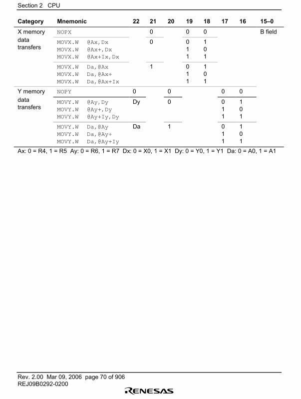
Section 2 CPU
Rev. 2.00 Mar 09, 2006 page 70 of 906REJ09B0292-0200
Category Mnemonic 22 21 20 19 18 17 16 15�0
X memory NOPX 0 0 0 B fielddatatransfers
MOVX.W @Ax,DxMOVX.W @Ax+,DxMOVX.W @Ax+Ix,Dx
0 011
101
MOVX.W Da,@AxMOVX.W Da,@Ax+MOVX.W Da,@Ax+Ix
1 011
101
Y memory NOPY 0 0 0 0datatransfers
MOVY.W @Ay,DyMOVY.W @Ay+,DyMOVY.W @Ay+Iy,Dy
Dy 0 011
101
MOVY.W Da,@AyMOVY.W Da,@Ay+MOVY.W Da,@Ay+Iy
Da 1 011
101
Ax: 0 = R4, 1 = R5 Ay: 0 = R6, 1 = R7 Dx: 0 = X0, 1 = X1 Dy: 0 = Y0, 1 = Y1 Da: 0 = A0, 1 = A1
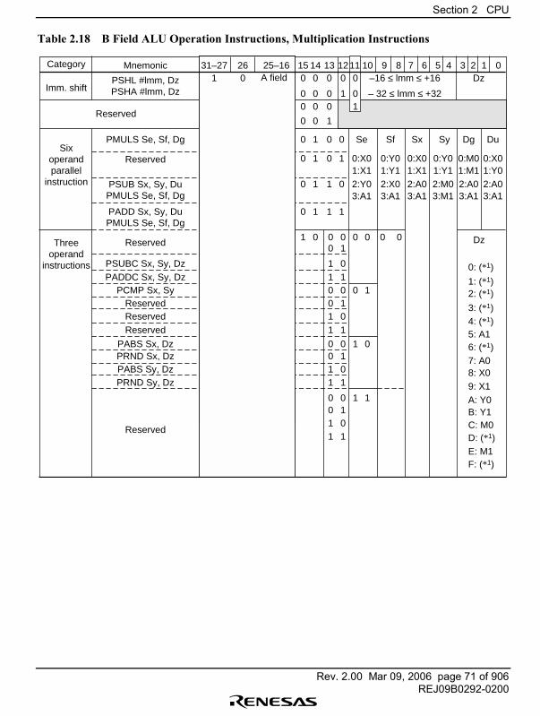
Section 2 CPU
Rev. 2.00 Mar 09, 2006 page 71 of 906REJ09B0292-0200
Table 2.18 B Field ALU Operation Instructions, Multiplication Instructions
Category Mnemonic 14 13 12 10 9 8 7 6 5 4 3 2 1 015Dz0 0 0
0 0 0
–16 ≤ lmm ≤ +16
– 32 ≤ lmm ≤ +32
0
1
0 Se Sf Sx Sy Dg Du
0 0 0
0 0 1
0 1 0
00 1 1
10 1 1
01 0 0 00 0 Dz
0: (*1)
1: (*1)2: (*1)
3: (*1)4: (*1)5: A16: (*1)7: A08: X09: X1A: Y0B: Y1C: M0D: (*1)E: M1F: (*1)
0
00 10
00 01
10
10
10
01
01
01
11
11
11
00 11100111
1 0:X01:X12:Y03:A1
0:X01:X12:A03:A1
0:X00:Y01:Y12:X03:A1
0:Y0 0:M01:Y01:Y1 1:M12:A02:M0 2:A03:A13:M1 3:A1
0 1 0
PSHL #lmm, DzPSHA #lmm, Dz
PMULS Se, Sf, Dg
Reserved
Reserved
Reserved
Reserved
ReservedReserved
PABS Sx, DzPRND Sx, Dz
PRND Sy, DzPABS Sy, Dz
Reserved
PSUBC Sx, Sy, DzPADDC Sx, Sy, Dz
PCMP Sx, Sy
PSUB Sx, Sy, DuPMULS Se, Sf, Dg
PADD Sx, Sy, DuPMULS Se, Sf, Dg
Imm. shift
Sixoperandparallel
instruction
Threeoperand
instructions
31–27 25–16261 0 A field
110
01
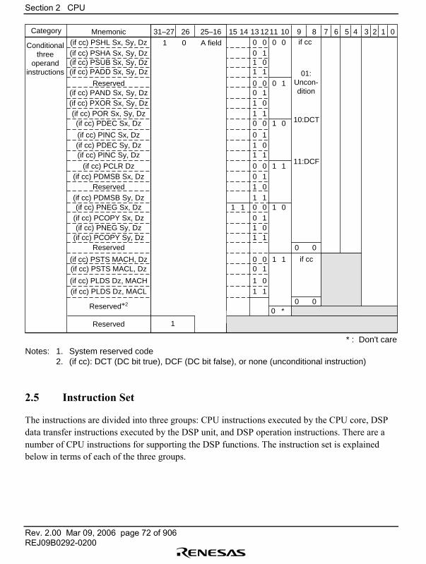
Section 2 CPU
Rev. 2.00 Mar 09, 2006 page 72 of 906REJ09B0292-0200
Category Mnemonic 14 13 12 10 9 8 7 6 5 4 3 2 1 015
1 1
00 00100111
00 1010011100 01
100111
00 111001
1100 01100111
00 1 if cc1
0 * 0 0
10
0111
Reserved
Reserved
Reserved
Reserved*2
Reserved
(if cc) PSHL Sx, Sy, Dz(if cc) PSHA Sx, Sy, Dz(if cc) PSUB Sx, Sy, Dz(if cc) PADD Sx, Sy, Dz
(if cc) PAND Sx, Sy, Dz(if cc) PXOR Sx, Sy, Dz(if cc) POR Sx, Sy, Dz
(if cc) PDEC Sx, Dz
(if cc) PDEC Sy, Dz(if cc) PINC Sx, Dz
(if cc) PINC Sy, Dz
(if cc) PCLR Dz(if cc) PDMSB Sx, Dz
(if cc) PDMSB Sy, Dz(if cc) PNEG Sx, Dz
(if cc) PNEG Sy, Dz(if cc) PCOPY Sx, Dz
(if cc) PCOPY Sy, Dz
(if cc) PSTS MACH, Dz(if cc) PSTS MACL, Dz
(if cc) PLDS Dz, MACL(if cc) PLDS Dz, MACH
Conditionalthree
operandinstructions
0 0
if cc
10:DCT
11:DCF
01:Uncon-dition
31–27 25–1626
1
11
1 0 A field
Notes: 1. System reserved code 2. (if cc): DCT (DC bit true), DCF (DC bit false), or none (unconditional instruction)
* : Don't care
2.5 Instruction Set
The instructions are divided into three groups: CPU instructions executed by the CPU core, DSPdata transfer instructions executed by the DSP unit, and DSP operation instructions. There are anumber of CPU instructions for supporting the DSP functions. The instruction set is explainedbelow in terms of each of the three groups.
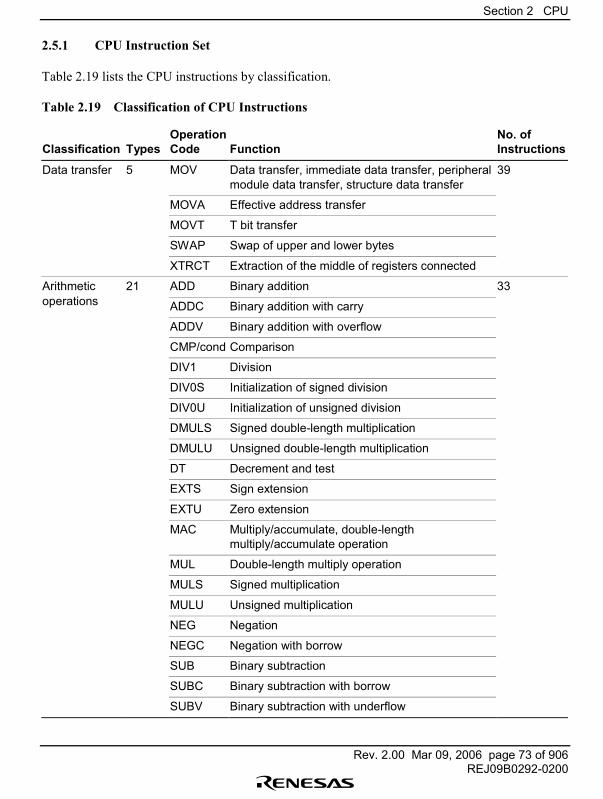
Section 2 CPU
Rev. 2.00 Mar 09, 2006 page 73 of 906REJ09B0292-0200
2.5.1 CPU Instruction Set
Table 2.19 lists the CPU instructions by classification.
Table 2.19 Classification of CPU Instructions
Classification TypesOperationCode Function
No. ofInstructions
Data transfer 5 MOV Data transfer, immediate data transfer, peripheralmodule data transfer, structure data transfer
39
MOVA Effective address transfer
MOVT T bit transfer
SWAP Swap of upper and lower bytes
XTRCT Extraction of the middle of registers connected
Arithmetic 21 ADD Binary addition 33operations ADDC Binary addition with carry
ADDV Binary addition with overflow
CMP/cond Comparison
DIV1 Division
DIV0S Initialization of signed division
DIV0U Initialization of unsigned division
DMULS Signed double-length multiplication
DMULU Unsigned double-length multiplication
DT Decrement and test
EXTS Sign extension
EXTU Zero extension
MAC Multiply/accumulate, double-lengthmultiply/accumulate operation
MUL Double-length multiply operation
MULS Signed multiplication
MULU Unsigned multiplication
NEG Negation
NEGC Negation with borrow
SUB Binary subtraction
SUBC Binary subtraction with borrow
SUBV Binary subtraction with underflow
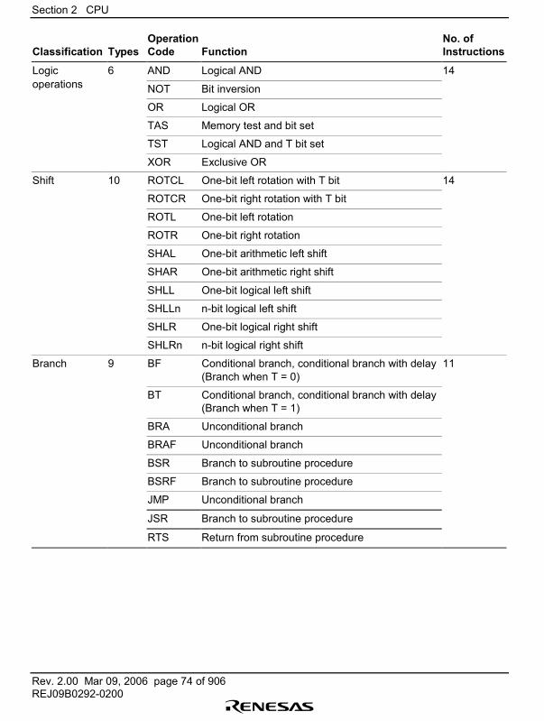
Section 2 CPU
Rev. 2.00 Mar 09, 2006 page 74 of 906REJ09B0292-0200
Classification TypesOperationCode Function
No. ofInstructions
Logic 6 AND Logical AND 14operations NOT Bit inversion
OR Logical OR
TAS Memory test and bit set
TST Logical AND and T bit set
XOR Exclusive OR
Shift 10 ROTCL One-bit left rotation with T bit 14
ROTCR One-bit right rotation with T bit
ROTL One-bit left rotation
ROTR One-bit right rotation
SHAL One-bit arithmetic left shift
SHAR One-bit arithmetic right shift
SHLL One-bit logical left shift
SHLLn n-bit logical left shift
SHLR One-bit logical right shift
SHLRn n-bit logical right shift
Branch 9 BF Conditional branch, conditional branch with delay(Branch when T = 0)
11
BT Conditional branch, conditional branch with delay(Branch when T = 1)
BRA Unconditional branch
BRAF Unconditional branch
BSR Branch to subroutine procedure
BSRF Branch to subroutine procedure
JMP Unconditional branch
JSR Branch to subroutine procedure
RTS Return from subroutine procedure
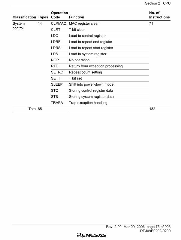
Section 2 CPU
Rev. 2.00 Mar 09, 2006 page 75 of 906REJ09B0292-0200
Classification TypesOperationCode Function
No. ofInstructions
System 14 CLRMAC MAC register clear 71control CLRT T bit clear
LDC Load to control register
LDRE Load to repeat end register
LDRS Load to repeat start register
LDS Load to system register
NOP No operation
RTE Return from exception processing
SETRC Repeat count setting
SETT T bit set
SLEEP Shift into power-down mode
STC Storing control register data
STS Storing system register data
TRAPA Trap exception handling
Total:65 182
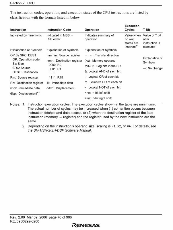
Section 2 CPU
Rev. 2.00 Mar 09, 2006 page 76 of 906REJ09B0292-0200
The instruction codes, operation, and execution states of the CPU instructions are listed byclassification with the formats listed in below.
Instruction Instruction Code OperationExecutionCycles T Bit
Indicated by mnemonic
Explanation of Symbols
OP.Sz SRC, DESTOP: Operation codeSz: SizeSRC: SourceDEST: Destination
Rm: Source register
Rn: Destination register
imm: Immediate data
disp: Displacement*2
Indicated in MSB ↔LSB order
Explanation of Symbols
mmmm: Source register
nnnn: Destination register0000: R00001: R1.........
1111: R15
iiii: Immediate data
dddd: Displacement
Indicates summary ofoperation
Explanation of Symbols
→, ←: Transfer direction
(xx): Memory operand
M/Q/T: Flag bits in the SR
&: Logical AND of each bit
|: Logical OR of each bit
^: Exclusive OR of each bit
~: Logical NOT of each bit
<<n: n-bit left shift
>>n: n-bit right shift
Value whenno waitstates areinserted*1
Value of T bitafterinstruction isexecuted
Explanation ofSymbols
�: No change
Notes: 1. Instruction execution cycles: The execution cycles shown in the table are minimums.The actual number of cycles may be increased when (1) contention occurs betweeninstruction fetches and data access, or (2) when the destination register of the loadinstruction (memory → register) and the register used by the next instruction are thesame.
2. Depending on the instruction�s operand size, scaling is ×1, ×2, or ×4. For details, seethe SH-1/SH-2/SH-DSP Software Manual.
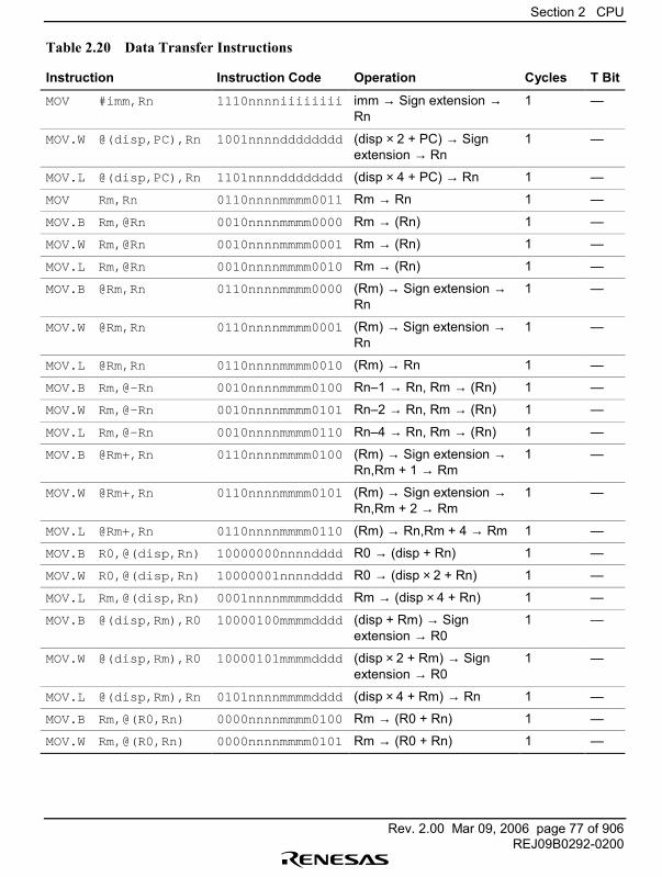
Section 2 CPU
Rev. 2.00 Mar 09, 2006 page 77 of 906REJ09B0292-0200
Table 2.20 Data Transfer Instructions
Instruction Instruction Code Operation Cycles T Bit
MOV #imm,Rn 1110nnnniiiiiiii imm → Sign extension →Rn
1 �
MOV.W @(disp,PC),Rn 1001nnnndddddddd (disp × 2 + PC) → Signextension → Rn
1 �
MOV.L @(disp,PC),Rn 1101nnnndddddddd (disp × 4 + PC) → Rn 1 �
MOV Rm,Rn 0110nnnnmmmm0011 Rm → Rn 1 �
MOV.B Rm,@Rn 0010nnnnmmmm0000 Rm → (Rn) 1 �
MOV.W Rm,@Rn 0010nnnnmmmm0001 Rm → (Rn) 1 �
MOV.L Rm,@Rn 0010nnnnmmmm0010 Rm → (Rn) 1 �
MOV.B @Rm,Rn 0110nnnnmmmm0000 (Rm) → Sign extension →Rn
1 �
MOV.W @Rm,Rn 0110nnnnmmmm0001 (Rm) → Sign extension →Rn
1 �
MOV.L @Rm,Rn 0110nnnnmmmm0010 (Rm) → Rn 1 �
MOV.B Rm,@–Rn 0010nnnnmmmm0100 Rn�1 → Rn, Rm → (Rn) 1 �
MOV.W Rm,@–Rn 0010nnnnmmmm0101 Rn�2 → Rn, Rm → (Rn) 1 �
MOV.L Rm,@–Rn 0010nnnnmmmm0110 Rn�4 → Rn, Rm → (Rn) 1 �
MOV.B @Rm+,Rn 0110nnnnmmmm0100 (Rm) → Sign extension →Rn,Rm + 1 → Rm
1 �
MOV.W @Rm+,Rn 0110nnnnmmmm0101 (Rm) → Sign extension →Rn,Rm + 2 → Rm
1 �
MOV.L @Rm+,Rn 0110nnnnmmmm0110 (Rm) → Rn,Rm + 4 → Rm 1 �
MOV.B R0,@(disp,Rn) 10000000nnnndddd R0 → (disp + Rn) 1 �
MOV.W R0,@(disp,Rn) 10000001nnnndddd R0 → (disp × 2 + Rn) 1 �
MOV.L Rm,@(disp,Rn) 0001nnnnmmmmdddd Rm → (disp × 4 + Rn) 1 �
MOV.B @(disp,Rm),R0 10000100mmmmdddd (disp + Rm) → Signextension → R0
1 �
MOV.W @(disp,Rm),R0 10000101mmmmdddd (disp × 2 + Rm) → Signextension → R0
1 �
MOV.L @(disp,Rm),Rn 0101nnnnmmmmdddd (disp × 4 + Rm) → Rn 1 �
MOV.B Rm,@(R0,Rn) 0000nnnnmmmm0100 Rm → (R0 + Rn) 1 �
MOV.W Rm,@(R0,Rn) 0000nnnnmmmm0101 Rm → (R0 + Rn) 1 �
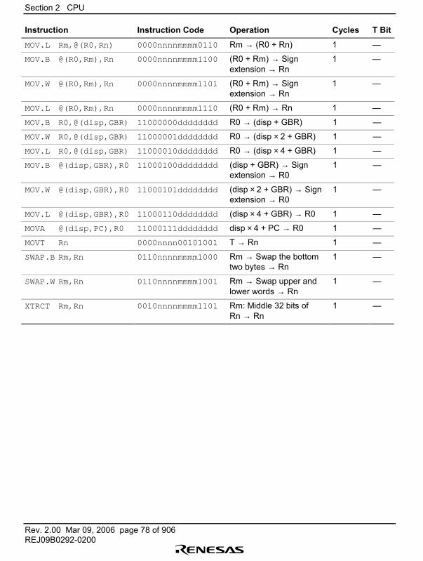
Section 2 CPU
Rev. 2.00 Mar 09, 2006 page 78 of 906REJ09B0292-0200
Instruction Instruction Code Operation Cycles T Bit
MOV.L Rm,@(R0,Rn) 0000nnnnmmmm0110 Rm → (R0 + Rn) 1 �
MOV.B @(R0,Rm),Rn 0000nnnnmmmm1100 (R0 + Rm) → Signextension → Rn
1 �
MOV.W @(R0,Rm),Rn 0000nnnnmmmm1101 (R0 + Rm) → Signextension → Rn
1 �
MOV.L @(R0,Rm),Rn 0000nnnnmmmm1110 (R0 + Rm) → Rn 1 �
MOV.B R0,@(disp,GBR) 11000000dddddddd R0 → (disp + GBR) 1 �
MOV.W R0,@(disp,GBR) 11000001dddddddd R0 → (disp × 2 + GBR) 1 �
MOV.L R0,@(disp,GBR) 11000010dddddddd R0 → (disp × 4 + GBR) 1 �
MOV.B @(disp,GBR),R0 11000100dddddddd (disp + GBR) → Signextension → R0
1 �
MOV.W @(disp,GBR),R0 11000101dddddddd (disp × 2 + GBR) → Signextension → R0
1 �
MOV.L @(disp,GBR),R0 11000110dddddddd (disp × 4 + GBR) → R0 1 �
MOVA @(disp,PC),R0 11000111dddddddd disp × 4 + PC → R0 1 �
MOVT Rn 0000nnnn00101001 T → Rn 1 �
SWAP.B Rm,Rn 0110nnnnmmmm1000 Rm → Swap the bottomtwo bytes → Rn
1 �
SWAP.W Rm,Rn 0110nnnnmmmm1001 Rm → Swap upper andlower words → Rn
1 �
XTRCT Rm,Rn 0010nnnnmmmm1101 Rm: Middle 32 bits ofRn → Rn
1 �
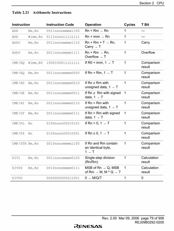
Section 2 CPU
Rev. 2.00 Mar 09, 2006 page 79 of 906REJ09B0292-0200
Table 2.21 Arithmetic Instructions
Instruction Instruction Code Operation Cycles T Bit
ADD Rm,Rn 0011nnnnmmmm1100 Rn + Rm → Rn 1 �
ADD #imm,Rn 0111nnnniiiiiiii Rn + imm → Rn 1 �
ADDC Rm,Rn 0011nnnnmmmm1110 Rn + Rm + T → Rn,Carry → T
1 Carry
ADDV Rm,Rn 0011nnnnmmmm1111 Rn + Rm → Rn,Overflow → T
1 Overflow
CMP/EQ #imm,R0 10001000iiiiiiii If R0 = imm, 1 → T 1 Comparisonresult
CMP/EQ Rm,Rn 0011nnnnmmmm0000 If Rn = Rm, 1 → T 1 Comparisonresult
CMP/HS Rm,Rn 0011nnnnmmmm0010 If Rn ≥ Rm withunsigned data, 1 → T
1 Comparisonresult
CMP/GE Rm,Rn 0011nnnnmmmm0011 If Rn ≥ Rm with signeddata, 1 → T
1 Comparisonresult
CMP/HI Rm,Rn 0011nnnnmmmm0110 If Rn > Rm withunsigned data, 1 → T
1 Comparisonresult
CMP/GT Rm,Rn 0011nnnnmmmm0111 If Rn > Rm with signeddata, 1 → T
1 Comparisonresult
CMP/PL Rn 0100nnnn00010101 If Rn > 0, 1 → T 1 Comparisonresult
CMP/PZ Rn 0100nnnn00010001 If Rn ≥ 0, 1 → T 1 Comparisonresult
CMP/STR Rm,Rn 0010nnnnmmmm1100 If Rn and Rm containan identical byte,1 → T
1 Comparisonresult
DIV1 Rm,Rn 0011nnnnmmmm0100 Single-step division(Rn/Rm)
1 Calculationresult
DIV0S Rm,Rn 0010nnnnmmmm0111 MSB of Rn → Q, MSBof Rm → M, M ^ Q → T
1 Calculationresult
DIV0U 0000000000011001 0 → M/Q/T 1 0
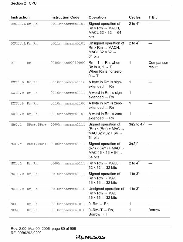
Section 2 CPU
Rev. 2.00 Mar 09, 2006 page 80 of 906REJ09B0292-0200
Instruction Instruction Code Operation Cycles T Bit
DMULS.L Rm,Rn 0011nnnnmmmm1101 Signed operation ofRn × Rm → MACH,MACL 32 × 32 → 64bits
2 to 4* �
DMULU.L Rm,Rn 0011nnnnmmmm0101 Unsigned operation ofRn × Rm → MACH,MACL 32 × 32 →64 bits
2 to 4* �
DT Rn 0100nnnn00010000 Rn � 1 → Rn, whenRn is 0, 1 → TWhen Rn is nonzero,0 → T
1 Comparisonresult
EXTS.B Rm,Rn 0110nnnnmmmm1110 A byte in Rm is sign-extended → Rn
1 �
EXTS.W Rm,Rn 0110nnnnmmmm1111 A word in Rm is sign-extended → Rn
1 �
EXTU.B Rm,Rn 0110nnnnmmmm1100 A byte in Rm is zero-extended → Rn
1 �
EXTU.W Rm,Rn 0110nnnnmmmm1101 A word in Rm is zero-extended → Rn
1 �
MAC.L @Rm+,@Rn+ 0000nnnnmmmm1111 Signed operation of(Rn) × (Rm) + MAC →MAC 32 × 32 + 64 →64 bits
3/(2 to 4)* �
MAC.W @Rm+,@Rn+ 0100nnnnmmmm1111 Signed operation of(Rn) × (Rm) + MAC →MAC 16 × 16 + 64 →64 bits
3/(2)* �
MUL.L Rm,Rn 0000nnnnmmmm0111 Rn × Rm → MACL,32 × 32 → 32 bits
2 to 4* �
MULS.W Rm,Rn 0010nnnnmmmm1111 Signed operation ofRn × Rm → MAC16 × 16 → 32 bits
1 to 3* �
MULU.W Rm,Rn 0010nnnnmmmm1110 Unsigned operation ofRn × Rm → MAC16 × 16 → 32 bits
1 to 3* �
NEG Rm,Rn 0110nnnnmmmm1011 0�Rm → Rn 1 �
NEGC Rm,Rn 0110nnnnmmmm1010 0�Rm�T → Rn,Borrow → T
1 Borrow
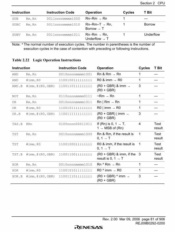
Section 2 CPU
Rev. 2.00 Mar 09, 2006 page 81 of 906REJ09B0292-0200
Instruction Instruction Code Operation Cycles T Bit
SUB Rm,Rn 0011nnnnmmmm1000 Rn�Rm → Rn 1 �
SUBC Rm,Rn 0011nnnnmmmm1010 Rn�Rm�T → Rn,Borrow → T
1 Borrow
SUBV Rm,Rn 0011nnnnmmmm1011 Rn�Rm → Rn,Underflow → T
1 Underflow
Note: * The normal number of execution cycles. The number in parentheses is the number ofexecution cycles in the case of contention with preceding or following instructions.
Table 2.22 Logic Operation Instructions
Instruction Instruction Code Operation Cycles T Bit
AND Rm,Rn 0010nnnnmmmm1001 Rn & Rm → Rn 1 �
AND #imm,R0 11001001iiiiiiii R0 & imm → R0 1 �
AND.B #imm,@(R0,GBR) 11001101iiiiiiii (R0 + GBR) & imm →(R0 + GBR)
3 �
NOT Rm,Rn 0110nnnnmmmm0111 ~Rm → Rn 1 �
OR Rm,Rn 0010nnnnmmmm1011 Rn | Rm → Rn 1 �
OR #imm,R0 11001011iiiiiiii R0 | imm → R0 1 �
OR.B #imm,@(R0,GBR) 11001111iiiiiiii (R0 + GBR) | imm →(R0 + GBR)
3 �
TAS.B @Rn 0100nnnn00011011 If (Rn) is 0, 1 → T,1 → MSB of (Rn)
4 Testresult
TST Rm,Rn 0010nnnnmmmm1000 Rn & Rm, if the result is0, 1 → T
1 Testresult
TST #imm,R0 11001000iiiiiiii R0 & imm, if the result is0, 1 → T
1 Testresult
TST.B #imm,@(R0,GBR) 11001100iiiiiiii (R0 + GBR) & imm, if theresult is 0, 1 → T
3 Testresult
XOR Rm,Rn 0010nnnnmmmm1010 Rn ^ Rm → Rn 1 �
XOR #imm,R0 11001010iiiiiiii R0 ^ imm → R0 1 �
XOR.B #imm,@(R0,GBR) 11001110iiiiiiii (R0 + GBR) ^ imm →(R0 + GBR)
3 �
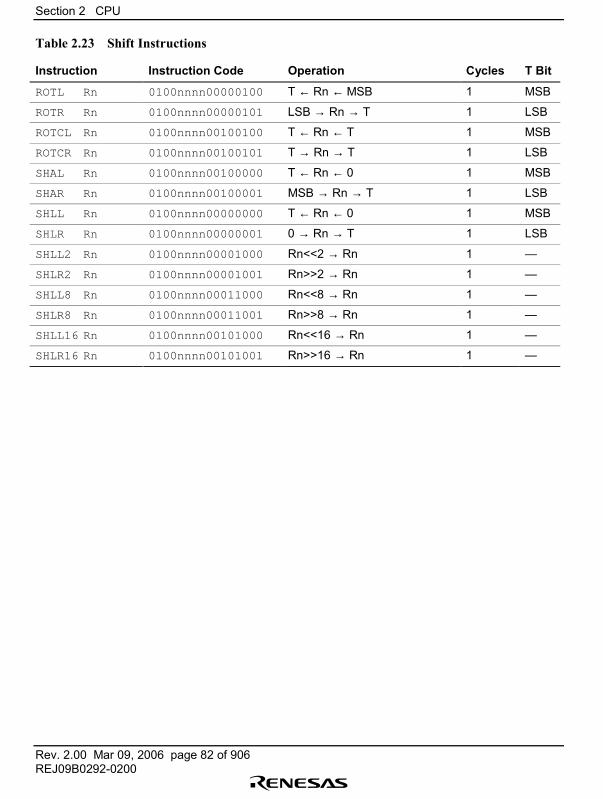
Section 2 CPU
Rev. 2.00 Mar 09, 2006 page 82 of 906REJ09B0292-0200
Table 2.23 Shift Instructions
Instruction Instruction Code Operation Cycles T Bit
ROTL Rn 0100nnnn00000100 T ← Rn ← MSB 1 MSB
ROTR Rn 0100nnnn00000101 LSB → Rn → T 1 LSB
ROTCL Rn 0100nnnn00100100 T ← Rn ← T 1 MSB
ROTCR Rn 0100nnnn00100101 T → Rn → T 1 LSB
SHAL Rn 0100nnnn00100000 T ← Rn ← 0 1 MSB
SHAR Rn 0100nnnn00100001 MSB → Rn → T 1 LSB
SHLL Rn 0100nnnn00000000 T ← Rn ← 0 1 MSB
SHLR Rn 0100nnnn00000001 0 → Rn → T 1 LSB
SHLL2 Rn 0100nnnn00001000 Rn<<2 → Rn 1 �
SHLR2 Rn 0100nnnn00001001 Rn>>2 → Rn 1 �
SHLL8 Rn 0100nnnn00011000 Rn<<8 → Rn 1 �
SHLR8 Rn 0100nnnn00011001 Rn>>8 → Rn 1 �
SHLL16 Rn 0100nnnn00101000 Rn<<16 → Rn 1 �
SHLR16 Rn 0100nnnn00101001 Rn>>16 → Rn 1 �
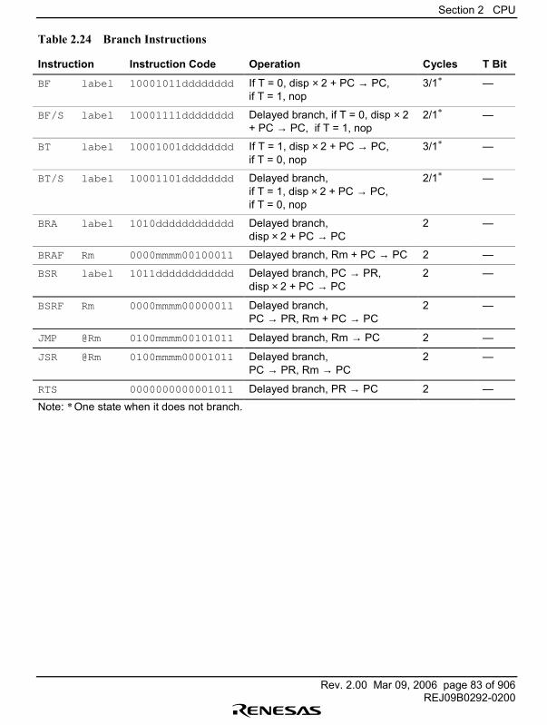
Section 2 CPU
Rev. 2.00 Mar 09, 2006 page 83 of 906REJ09B0292-0200
Table 2.24 Branch Instructions
Instruction Instruction Code Operation Cycles T Bit
BF label 10001011dddddddd If T = 0, disp × 2 + PC → PC,if T = 1, nop
3/1* �
BF/S label 10001111dddddddd Delayed branch, if T = 0, disp × 2+ PC → PC, if T = 1, nop
2/1* �
BT label 10001001dddddddd If T = 1, disp × 2 + PC → PC,if T = 0, nop
3/1* �
BT/S label 10001101dddddddd Delayed branch,if T = 1, disp × 2 + PC → PC,if T = 0, nop
2/1* �
BRA label 1010dddddddddddd Delayed branch,disp × 2 + PC → PC
2 �
BRAF Rm 0000mmmm00100011 Delayed branch, Rm + PC → PC 2 �
BSR label 1011dddddddddddd Delayed branch, PC → PR,disp × 2 + PC → PC
2 �
BSRF Rm 0000mmmm00000011 Delayed branch,PC → PR, Rm + PC → PC
2 �
JMP @Rm 0100mmmm00101011 Delayed branch, Rm → PC 2 �
JSR @Rm 0100mmmm00001011 Delayed branch,PC → PR, Rm → PC
2 �
RTS 0000000000001011 Delayed branch, PR → PC 2 �Note: * One state when it does not branch.
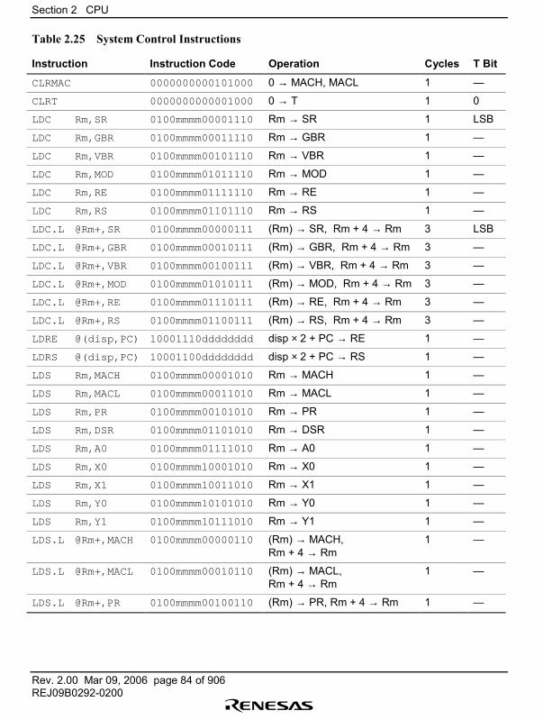
Section 2 CPU
Rev. 2.00 Mar 09, 2006 page 84 of 906REJ09B0292-0200
Table 2.25 System Control Instructions
Instruction Instruction Code Operation Cycles T Bit
CLRMAC 0000000000101000 0 → MACH, MACL 1 �
CLRT 0000000000001000 0 → T 1 0
LDC Rm,SR 0100mmmm00001110 Rm → SR 1 LSB
LDC Rm,GBR 0100mmmm00011110 Rm → GBR 1 �
LDC Rm,VBR 0100mmmm00101110 Rm → VBR 1 �
LDC Rm,MOD 0100mmmm01011110 Rm → MOD 1 �
LDC Rm,RE 0100mmmm01111110 Rm → RE 1 �
LDC Rm,RS 0100mmmm01101110 Rm → RS 1 �
LDC.L @Rm+,SR 0100mmmm00000111 (Rm) → SR, Rm + 4 → Rm 3 LSB
LDC.L @Rm+,GBR 0100mmmm00010111 (Rm) → GBR, Rm + 4 → Rm 3 �
LDC.L @Rm+,VBR 0100mmmm00100111 (Rm) → VBR, Rm + 4 → Rm 3 �
LDC.L @Rm+,MOD 0100mmmm01010111 (Rm) → MOD, Rm + 4 → Rm 3 �
LDC.L @Rm+,RE 0100mmmm01110111 (Rm) → RE, Rm + 4 → Rm 3 �
LDC.L @Rm+,RS 0100mmmm01100111 (Rm) → RS, Rm + 4 → Rm 3 �
LDRE @(disp,PC) 10001110dddddddd disp × 2 + PC → RE 1 �
LDRS @(disp,PC) 10001100dddddddd disp × 2 + PC → RS 1 �
LDS Rm,MACH 0100mmmm00001010 Rm → MACH 1 �
LDS Rm,MACL 0100mmmm00011010 Rm → MACL 1 �
LDS Rm,PR 0100mmmm00101010 Rm → PR 1 �
LDS Rm,DSR 0100mmmm01101010 Rm → DSR 1 �
LDS Rm,A0 0100mmmm01111010 Rm → A0 1 �
LDS Rm,X0 0100mmmm10001010 Rm → X0 1 �
LDS Rm,X1 0100mmmm10011010 Rm → X1 1 �
LDS Rm,Y0 0100mmmm10101010 Rm → Y0 1 �
LDS Rm,Y1 0100mmmm10111010 Rm → Y1 1 �
LDS.L @Rm+,MACH 0100mmmm00000110 (Rm) → MACH,Rm + 4 → Rm
1 �
LDS.L @Rm+,MACL 0100mmmm00010110 (Rm) → MACL,Rm + 4 → Rm
1 �
LDS.L @Rm+,PR 0100mmmm00100110 (Rm) → PR, Rm + 4 → Rm 1 �

Section 2 CPU
Rev. 2.00 Mar 09, 2006 page 85 of 906REJ09B0292-0200
Instruction Instruction Code Operation Cycles T Bit
LDS.L @Rm+,DSR 0100mmmm01100110 (Rm) → DSR, Rm + 4 → Rm 1 �
LDS.L @Rm+,A0 0100mmmm01110110 (Rm) → A0, Rm + 4 → Rm 1 �
LDS.L @Rm+,X0 0100mmmm10000110 (Rm) → X0, Rm + 4 → Rm 1 �
LDS.L @Rm+,X1 0100mmmm10010110 (Rm) → X1, Rm + 4 → Rm 1 �
LDS.L @Rm+,Y0 0100mmmm10100110 (Rm) → Y0, Rm + 4 → Rm 1 �
LDS.L @Rm+,Y1 0100mmmm10110110 (Rm) → Y1, Rm + 4 → Rm 1 �
NOP 0000000000001001 No operation 1 �
RTE 0000000000101011 Delayed branch,stack area → PC/SR
4 LSB
SETRC Rm 0100mmmm00010100 RE�RS operation result(repeat status) → RF1, RF0
Rm[11:0] → RC (SR[27:16])
1 �
SETRC #imm 10000010iiiiiiii RE�RS operation result(repeat status) → RF1, RF0
imm → RC (SR[23:16]),0 → SR[27:24]
1 1
SETT 0000000000011000 1 → T 1 1
SLEEP 0000000000011011 Sleep 3* �
STC SR,Rn 0000nnnn00000010 SR → Rn 1 �
STC GBR,Rn 0000nnnn00010010 GBR → Rn 1 �
STC VBR,Rn 0000nnnn00100010 VBR → Rn 1 �
STC MOD,Rn 0000nnnn01010010 MOD → Rn 1 �
STC RE,Rn 0000nnnn01110010 RE → Rn 1 �
STC RS,Rn 0000nnnn01100010 RS → Rn 1 �
STC.L SR,@–Rn 0100nnnn00000011 Rn�4 → Rn, SR → (Rn) 2 �
STC.L GBR,@–Rn 0100nnnn00010011 Rn�4 → Rn, GBR → (Rn) 2 �
STC.L VBR,@–Rn 0100nnnn00100011 Rn�4 → Rn, VBR → (Rn) 2 �
STC.L MOD,@–Rn 0100nnnn01010011 Rn�4 → Rn, MOD → (Rn) 2 �
STC.L RE,@–Rn 0100nnnn01110011 Rn�4 → Rn, RE → (Rn) 2 �
STC.L RS,@–Rn 0100nnnn01100011 Rn�4 → Rn, RS → (Rn) 2 �
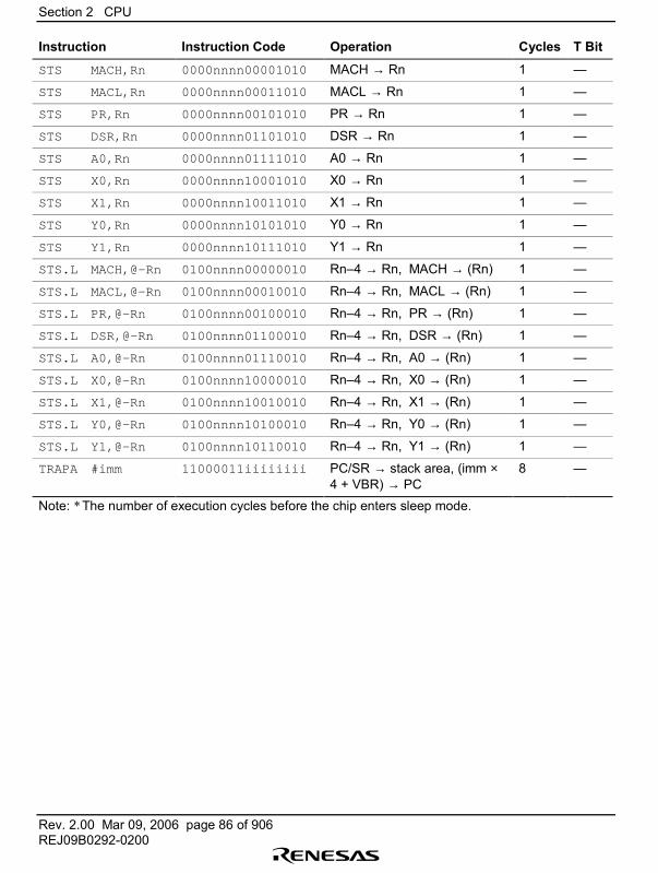
Section 2 CPU
Rev. 2.00 Mar 09, 2006 page 86 of 906REJ09B0292-0200
Instruction Instruction Code Operation Cycles T Bit
STS MACH,Rn 0000nnnn00001010 MACH → Rn 1 �
STS MACL,Rn 0000nnnn00011010 MACL → Rn 1 �
STS PR,Rn 0000nnnn00101010 PR → Rn 1 �
STS DSR,Rn 0000nnnn01101010 DSR → Rn 1 �
STS A0,Rn 0000nnnn01111010 A0 → Rn 1 �
STS X0,Rn 0000nnnn10001010 X0 → Rn 1 �
STS X1,Rn 0000nnnn10011010 X1 → Rn 1 �
STS Y0,Rn 0000nnnn10101010 Y0 → Rn 1 �
STS Y1,Rn 0000nnnn10111010 Y1 → Rn 1 �
STS.L MACH,@–Rn 0100nnnn00000010 Rn�4 → Rn, MACH → (Rn) 1 �
STS.L MACL,@–Rn 0100nnnn00010010 Rn�4 → Rn, MACL → (Rn) 1 �
STS.L PR,@–Rn 0100nnnn00100010 Rn�4 → Rn, PR → (Rn) 1 �
STS.L DSR,@–Rn 0100nnnn01100010 Rn�4 → Rn, DSR → (Rn) 1 �
STS.L A0,@–Rn 0100nnnn01110010 Rn�4 → Rn, A0 → (Rn) 1 �
STS.L X0,@–Rn 0100nnnn10000010 Rn�4 → Rn, X0 → (Rn) 1 �
STS.L X1,@–Rn 0100nnnn10010010 Rn�4 → Rn, X1 → (Rn) 1 �
STS.L Y0,@–Rn 0100nnnn10100010 Rn�4 → Rn, Y0 → (Rn) 1 �
STS.L Y1,@–Rn 0100nnnn10110010 Rn�4 → Rn, Y1 → (Rn) 1 �
TRAPA #imm 11000011iiiiiiii PC/SR → stack area, (imm ×4 + VBR) → PC
8 �
Note: * The number of execution cycles before the chip enters sleep mode.
Section 2 CPU
Rev. 2.00 Mar 09, 2006 page 87 of 906REJ09B0292-0200
Precautions Concerning the Number of Instruction Execution Cycles: The execution cycleslisted in the tables are minimum values. In practice, the number of execution cycles increasesunder such conditions as 1) when the instruction fetch is in contention with a data access, 2) whenthe destination register of a load instruction (memory → register) is the same as the register usedby the next instruction, 3) when the branch destination address of a branch instruction is a 4n + 2address.
CPU Instructions That Support DSP Functions: A number of system control instructions havebeen added to the CPU core instructions to support DSP functions. The RS, RE and MODregisters have been added to support repeat control and modulo addressing, and the repeat counter(RC) has been added to the status register (SR). The LDC and STC instructions have been addedin order to access the aforementioned. The LDS and STS instructions have been added in order toaccess the DSP registers DSR, A0, X0, X1, Y0 and Y1.
The SETRC instruction has been added to set the repeat counter (RC, bits 27 to 16) and repeatflags (RF1, RF0, bits 3 and 2) of the SR register. When the SETRC instruction operand isimmediate, the 8-bit immediate data is stored in bits 23 to 16 of the SR register and bits 27 to 24are cleared to 0. When the operand is a register, bits 11 to 0 (12 bits) of the register are stored inbits 27 to 16 of the SR register. Additionally, the status of 1 instruction repeat (00), 2 instructionrepeat (01), 3 instruction repeat (11) or 4 instruction or greater repeat (10) is set from the RS andRE set values.
In addition to the LDC instruction, the LDRS and LDRE instructions have been added forestablishing the repeat start and repeat end addresses in the RS and RE registers.
The added instructions are listed in table 2.26.
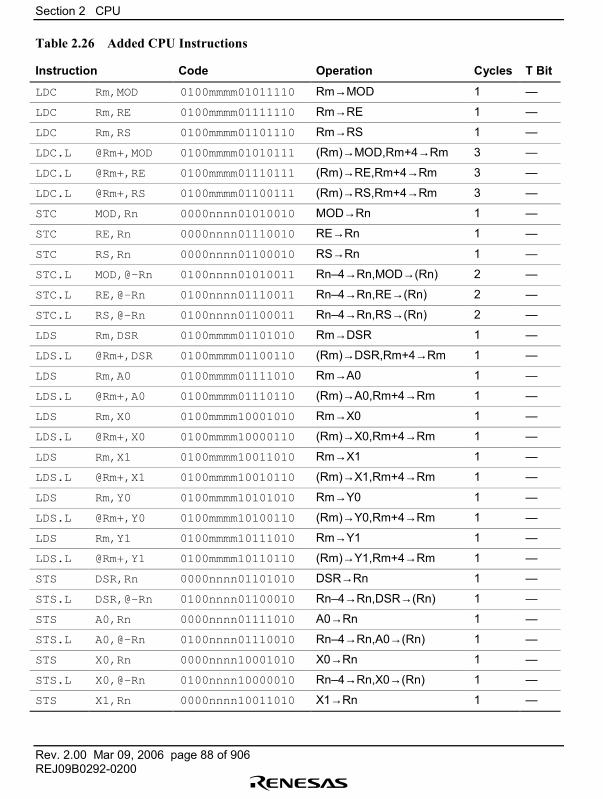
Section 2 CPU
Rev. 2.00 Mar 09, 2006 page 88 of 906REJ09B0292-0200
Table 2.26 Added CPU Instructions
Instruction Code Operation Cycles T Bit
LDC Rm,MOD 0100mmmm01011110 Rm→MOD 1 �
LDC Rm,RE 0100mmmm01111110 Rm→RE 1 �
LDC Rm,RS 0100mmmm01101110 Rm→RS 1 �
LDC.L @Rm+,MOD 0100mmmm01010111 (Rm)→MOD,Rm+4→Rm 3 �
LDC.L @Rm+,RE 0100mmmm01110111 (Rm)→RE,Rm+4→Rm 3 �
LDC.L @Rm+,RS 0100mmmm01100111 (Rm)→RS,Rm+4→Rm 3 �
STC MOD,Rn 0000nnnn01010010 MOD→Rn 1 �
STC RE,Rn 0000nnnn01110010 RE→Rn 1 �
STC RS,Rn 0000nnnn01100010 RS→Rn 1 �
STC.L MOD,@-Rn 0100nnnn01010011 Rn�4→Rn,MOD→(Rn) 2 �
STC.L RE,@-Rn 0100nnnn01110011 Rn�4→Rn,RE→(Rn) 2 �
STC.L RS,@-Rn 0100nnnn01100011 Rn�4→Rn,RS→(Rn) 2 �
LDS Rm,DSR 0100mmmm01101010 Rm→DSR 1 �
LDS.L @Rm+,DSR 0100mmmm01100110 (Rm)→DSR,Rm+4→Rm 1 �
LDS Rm,A0 0100mmmm01111010 Rm→A0 1 �
LDS.L @Rm+,A0 0100mmmm01110110 (Rm)→A0,Rm+4→Rm 1 �
LDS Rm,X0 0100mmmm10001010 Rm→X0 1 �
LDS.L @Rm+,X0 0100mmmm10000110 (Rm)→X0,Rm+4→Rm 1 �
LDS Rm,X1 0100mmmm10011010 Rm→X1 1 �
LDS.L @Rm+,X1 0100mmmm10010110 (Rm)→X1,Rm+4→Rm 1 �
LDS Rm,Y0 0100mmmm10101010 Rm→Y0 1 �
LDS.L @Rm+,Y0 0100mmmm10100110 (Rm)→Y0,Rm+4→Rm 1 �
LDS Rm,Y1 0100mmmm10111010 Rm→Y1 1 �
LDS.L @Rm+,Y1 0100mmmm10110110 (Rm)→Y1,Rm+4→Rm 1 �
STS DSR,Rn 0000nnnn01101010 DSR→Rn 1 �
STS.L DSR,@-Rn 0100nnnn01100010 Rn�4→Rn,DSR→(Rn) 1 �
STS A0,Rn 0000nnnn01111010 A0→Rn 1 �
STS.L A0,@-Rn 0100nnnn01110010 Rn�4→Rn,A0→(Rn) 1 �
STS X0,Rn 0000nnnn10001010 X0→Rn 1 �
STS.L X0,@-Rn 0100nnnn10000010 Rn�4→Rn,X0→(Rn) 1 �
STS X1,Rn 0000nnnn10011010 X1→Rn 1 �
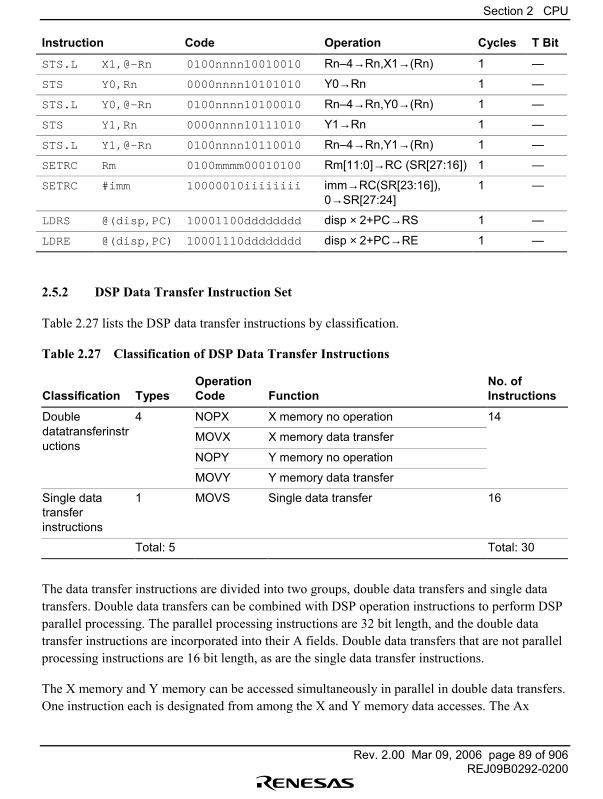
Section 2 CPU
Rev. 2.00 Mar 09, 2006 page 89 of 906REJ09B0292-0200
Instruction Code Operation Cycles T Bit
STS.L X1,@-Rn 0100nnnn10010010 Rn�4→Rn,X1→(Rn) 1 �
STS Y0,Rn 0000nnnn10101010 Y0→Rn 1 �
STS.L Y0,@-Rn 0100nnnn10100010 Rn�4→Rn,Y0→(Rn) 1 �
STS Y1,Rn 0000nnnn10111010 Y1→Rn 1 �
STS.L Y1,@-Rn 0100nnnn10110010 Rn�4→Rn,Y1→(Rn) 1 �
SETRC Rm 0100mmmm00010100 Rm[11:0]→RC (SR[27:16]) 1 �
SETRC #imm 10000010iiiiiiii imm→RC(SR[23:16]),0→SR[27:24]
1 �
LDRS @(disp,PC) 10001100dddddddd disp × 2+PC→RS 1 �
LDRE @(disp,PC) 10001110dddddddd disp × 2+PC→RE 1 �
2.5.2 DSP Data Transfer Instruction Set
Table 2.27 lists the DSP data transfer instructions by classification.
Table 2.27 Classification of DSP Data Transfer Instructions
Classification TypesOperationCode Function
No. ofInstructions
4 NOPX X memory no operation 14
MOVX X memory data transfer
Doubledatatransferinstructions
NOPY Y memory no operation
MOVY Y memory data transfer
Single datatransferinstructions
1 MOVS Single data transfer 16
Total: 5 Total: 30
The data transfer instructions are divided into two groups, double data transfers and single datatransfers. Double data transfers can be combined with DSP operation instructions to perform DSPparallel processing. The parallel processing instructions are 32 bit length, and the double datatransfer instructions are incorporated into their A fields. Double data transfers that are not parallelprocessing instructions are 16 bit length, as are the single data transfer instructions.
The X memory and Y memory can be accessed simultaneously in parallel in double data transfers.One instruction each is designated from among the X and Y memory data accesses. The Ax
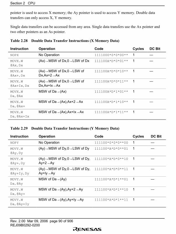
Section 2 CPU
Rev. 2.00 Mar 09, 2006 page 90 of 906REJ09B0292-0200
pointer is used to access X memory; the Ay pointer is used to access Y memory. Double datatransfers can only access X, Y memory.
Single data transfers can be accessed from any area. Single data transfers use the Ax pointer andtwo other pointers as an As pointer.
Table 2.28 Double Data Transfer Instructions (X Memory Data)
Instruction Operation Code Cycles DC Bit
NOPX No Operation 1111000*0*0*00** 1 �
MOVX.W@Ax,Dx
(Ax)→MSW of Dx,0→LSW of Dx 111100A*D*0*01** 1 �
MOVX.W@Ax+,Dx
(Ax)→MSW of Dx,0→LSW ofDx,Ax+2→Ax
111100A*D*0*10** 1 �
MOVX.W@Ax+Ix,Dx
(Ax)→MSW of Dx,0→LSW ofDx,Ax+Ix→Ax
111100A*D*0*11** 1 �
MOVX.WDa,@Ax
MSW of Da→(Ax) 111100A*D*1*01** 1 �
MOVX.WDa,@Ax+
MSW of Da→(Ax),Ax+2→Ax 111100A*D*1*10** 1 �
MOVX.WDa,@Ax+Ix
MSW of Da→(Ax),Ax+Ix→Ax 111100A*D*1*11** 1 �
Table 2.29 Double Data Transfer Instructions (Y Memory Data)
Instruction Operation Code Cycles DC Bit
NOPY No Operation 111100*0*0*0**00 1 �
MOVY.W@Ay,Dy
(Ay)→MSW of Dy,0→LSW of Dy 111100*A*D*0**01 1 �
MOVY.W@Ay+,Dy
(Ay)→MSW of Dy,0→LSW of Dy,Ay+2→Ay
111100*A*D*0**10 1 �
MOVY.W@Ay+Iy,Dy
(Ay)→MSW of Dy,0→LSW of Dy,Ay+Iy→Ay
111100*A*D*0**11 1 �
MOVY.WDa,@Ay
MSW of Da→(Ay) 111100*A*D*1**01 1 �
MOVY.WDa,@Ay+
MSW of Da→(Ay),Ay+2→Ay 111100*A*D*1**10 1 �
MOVY.WDa,@Ay+Iy
MSW of Da→(Ay),Ay+Iy→Ay 111100*A*D*1**11 1 �
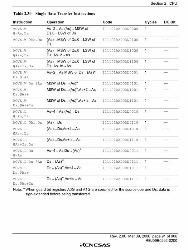
Section 2 CPU
Rev. 2.00 Mar 09, 2006 page 91 of 906REJ09B0292-0200
Table 2.30 Single Data Transfer Instructions
Instruction Operation Code Cycles DC Bit
MOVS.W@-As,Ds
As�2→As,(As)→MSW ofDs,0→LSW of Ds
111101AADDDD0000 1 �
MOVS.W @As,Ds (As)→MSW of Ds,0→LSW ofDs
111101AADDDD0100 1 �
MOVS.W@As+,Ds
(As)→MSW of Ds,0→LSW ofDs, As+2→As
111101AADDDD1000 1 �
MOVS.W@As+Ix,Ds
(As)→MSW of Ds,0→LSW ofDs, As+Ix→As
111101AADDDD1100 1 �
MOVS.WDs,@-As
As�2→As,MSW of Ds→(As)* 111101AADDDD0001 1 �
MOVS.W Ds,@As MSW of Ds→(As)* 111101AADDDD0101 1 �
MOVS.WDs,@As+
MSW of Ds→(As)*,As+2→As 111101AADDDD1001 1 �
MOVS.WDs,@As+Is
MSW of Ds→(As)*,As+Is→As 111101AADDDD1101 1 �
MOVS.L@-As,Ds
As�4→As,(As)→Ds 111101AADDDD0010 1 �
MOVS.L @As,Ds (As)→Ds 111101AADDDD0110 1 �
MOVS.L@As+,Ds
(As)→Ds,As+4→As 111101AADDDD1010 1 �
MOVS.L@As+Is,Ds
(As)→Ds,As+Is→As 111101AADDDD1110 1 �
MOVS.L Ds,@-As
As�4→As,Ds→(As)* 111101AADDDD0011 1 �
MOVS.L Ds,@As Ds→(As)* 111101AADDDD0111 1 �
MOVS.LDs,@As+
Ds→(As)*,As+4→As 111101AADDDD1011 1 �
MOVS.LDs,@As+Is
Ds→(As)*,As+Is→As 111101AADDDD1111 1 �
Note: * When guard bit registers A0G and A1G are specified for the source operand Ds, data issign-extended before being transferred.
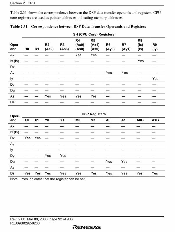
Section 2 CPU
Rev. 2.00 Mar 09, 2006 page 92 of 906REJ09B0292-0200
Table 2.31 shows the correspondence between the DSP data transfer operands and registers. CPUcore registers are used as pointer addresses indicating memory addresses.
Table 2.31 Correspondence between DSP Data Transfer Operands and Registers
SH (CPU Core) Registers
Oper-and R0 R1
R2(As2)
R3(As3)
R4(Ax0)(As0)
R5(Ax1)(As0)
R6(Ay0)
R7(Ay1)
R8(Ix)(Is)
R9(Iy)
Ax � � � � Yes Yes � � � �
Ix (Is) � � � � � � � � Yes �
Dx � � � � � � � � � �
Ay � � � � � � Yes Yes � �
Iy � � � � � � � � � Yes
Dy � � � � � � � � � �
Da � � � � � � � � � �
As � � Yes Yes Yes Yes � � � �
Ds � � � � � � � � � �
Oper- DSP Registers
and X0 X1 Y0 Y1 M0 M1 A0 A1 A0G A1G
Ax � � � � � � � � � �
Ix (Is) � � � � � � � � � �
Dx Yes Yes � � � � � � � �
Ay � � � � � � � � � �
Iy � � � � � � � � � �
Dy � � Yes Yes � � � � � �
Da � � � � � � Yes Yes � �
As � � � � � � � � � �
Ds Yes Yes Yes Yes Yes Yes Yes Yes Yes YesNote: Yes indicates that the register can be set.
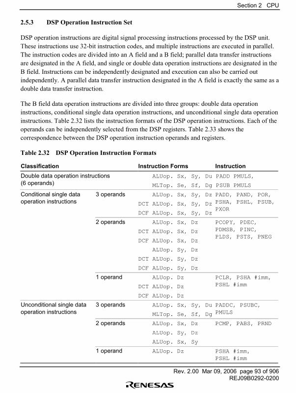
Section 2 CPU
Rev. 2.00 Mar 09, 2006 page 93 of 906REJ09B0292-0200
2.5.3 DSP Operation Instruction Set
DSP operation instructions are digital signal processing instructions processed by the DSP unit.These instructions use 32-bit instruction codes, and multiple instructions are executed in parallel.The instruction codes are divided into an A field and a B field; parallel data transfer instructionsare designated in the A field, and single or double data operation instructions are designated in theB field. Instructions can be independently designated and execution can also be carried outindependently. A parallel data transfer instruction designated in the A field is exactly the same as adouble data transfer instruction.
The B field data operation instructions are divided into three groups: double data operationinstructions, conditional single data operation instructions, and unconditional single data operationinstructions. Table 2.32 lists the instruction formats of the DSP operation instructions. Each of theoperands can be independently selected from the DSP registers. Table 2.33 shows thecorrespondence between the DSP operation instruction operands and registers.
Table 2.32 DSP Operation Instruction Formats
Classification Instruction Forms InstructionDouble data operation instructions(6 operands)
ALUop. Sx, Sy, Du
MLTop. Se, Sf, Dg
PADD PMULS,
PSUB PMULS
Conditional single dataoperation instructions
3 operands ALUop. Sx, Sy, Dz
DCT ALUop. Sx, Sy, Dz
DCF ALUop. Sx, Sy, Dz
PADD, PAND, POR,PSHA, PSHL, PSUB,PXOR
2 operands ALUop. Sx, Dz
DCT ALUop. Sx, Dz
DCF ALUop. Sx, Dz
ALUop. Sy, Dz
DCT ALUop. Sy, Dz
DCF ALUop. Sy, Dz
PCOPY, PDEC,PDMSB, PINC,PLDS, PSTS, PNEG
1 operand ALUop. Dz
DCT ALUop. Dz
DCF ALUop. Dz
PCLR, PSHA #imm,PSHL #imm
Unconditional single dataoperation instructions
3 operands ALUop. Sx, Sy, Du
MLTop. Se, Sf, Dg
PADDC, PSUBC,PMULS
2 operands ALUop. Sx, Dz
ALUop. Sy, Dz
ALUop. Sx, Sy
PCMP, PABS, PRND
1 operand ALUop. Dz PSHA #imm,PSHL #imm
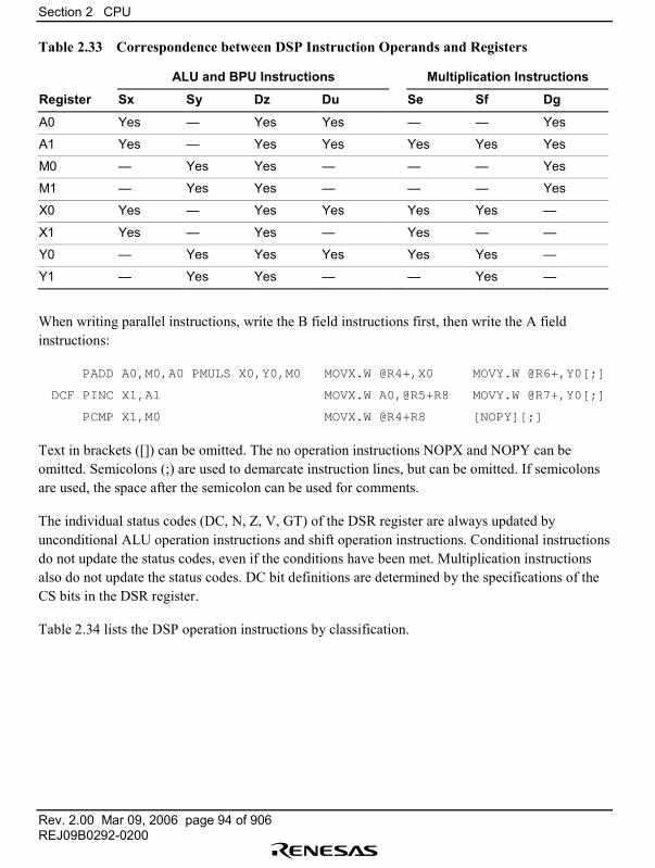
Section 2 CPU
Rev. 2.00 Mar 09, 2006 page 94 of 906REJ09B0292-0200
Table 2.33 Correspondence between DSP Instruction Operands and Registers
ALU and BPU Instructions Multiplication Instructions
Register Sx Sy Dz Du Se Sf Dg
A0 Yes � Yes Yes � � Yes
A1 Yes � Yes Yes Yes Yes Yes
M0 � Yes Yes � � � Yes
M1 � Yes Yes � � � Yes
X0 Yes � Yes Yes Yes Yes �
X1 Yes � Yes � Yes � �
Y0 � Yes Yes Yes Yes Yes �
Y1 � Yes Yes � � Yes �
When writing parallel instructions, write the B field instructions first, then write the A fieldinstructions:
PADD A0,M0,A0 PMULS X0,Y0,M0 MOVX.W @R4+,X0 MOVY.W @R6+,Y0[;]
DCF PINC X1,A1 MOVX.W A0,@R5+R8 MOVY.W @R7+,Y0[;]
PCMP X1,M0 MOVX.W @R4+R8 [NOPY][;]
Text in brackets ([]) can be omitted. The no operation instructions NOPX and NOPY can beomitted. Semicolons (;) are used to demarcate instruction lines, but can be omitted. If semicolonsare used, the space after the semicolon can be used for comments.
The individual status codes (DC, N, Z, V, GT) of the DSR register are always updated byunconditional ALU operation instructions and shift operation instructions. Conditional instructionsdo not update the status codes, even if the conditions have been met. Multiplication instructionsalso do not update the status codes. DC bit definitions are determined by the specifications of theCS bits in the DSR register.
Table 2.34 lists the DSP operation instructions by classification.
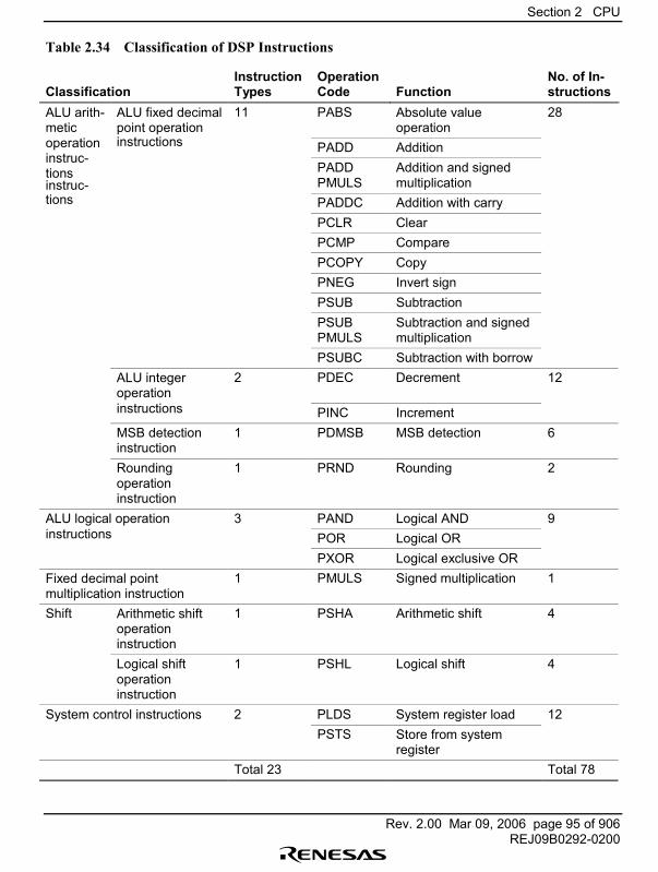
Section 2 CPU
Rev. 2.00 Mar 09, 2006 page 95 of 906REJ09B0292-0200
Table 2.34 Classification of DSP Instructions
ClassificationInstructionTypes
OperationCode Function
No. of In-structions
ALU fixed decimalpoint operation
11 PABS Absolute valueoperation
28
instructions PADD Addition
ALU arith-meticoperationinstruc-tions PADD
PMULSAddition and signedmultiplicationinstruc-
PADDC Addition with carrytions
PCLR ClearPCMP ComparePCOPY CopyPNEG Invert signPSUB SubtractionPSUBPMULS
Subtraction and signedmultiplication
PSUBC Subtraction with borrowALU integeroperation
2 PDEC Decrement 12
instructions PINC IncrementMSB detectioninstruction
1 PDMSB MSB detection 6
Roundingoperationinstruction
1 PRND Rounding 2
ALU logical operation 3 PAND Logical AND 9instructions POR Logical OR
PXOR Logical exclusive ORFixed decimal pointmultiplication instruction
1 PMULS Signed multiplication 1
Shift Arithmetic shiftoperationinstruction
1 PSHA Arithmetic shift 4
Logical shiftoperationinstruction
1 PSHL Logical shift 4
System control instructions 2 PLDS System register load 12PSTS Store from system
registerTotal 23 Total 78
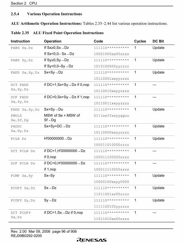
Section 2 CPU
Rev. 2.00 Mar 09, 2006 page 96 of 906REJ09B0292-0200
2.5.4 Various Operation Instructions
ALU Arithmetic Operation Instructions: Tables 2.35�2.44 list various operation instructions.
Table 2.35 ALU Fixed Point Operation Instructions
Instruction Operation Code Cycles DC Bit
PABS Sx,Dz If Sx≥0,Sx→Dz
If Sx<0,0� Sx→Dz
111110**********
10001000xx00zzzz
1 Update
PABS Sy,Dz If Sy≥0,Sy→Dz
If Sy<0,0�Sy→Dz
111110**********
1010100000yyzzzz
1 Update
PADD Sx,Sy,Dz Sx+Sy→Dz 111110**********
10110001xxyyzzzz
1 Update
DCT PADDSx,Sy,Dz
if DC=1,Sx+Sy→Dz if 0,nop 111110**********
10110010xxyyzzzz
1 �
DCF PADDSx,Sy,Dz
if DC=0,Sx+Sy→Dz if 1,nop 111110**********
10110011xxyyzzzz
1 �
PADD Sx,Sy,Du
PMULSSe,Sf,Dg
Sx+Sy→Du
MSW of Se × MSW ofSf→Dg
111110**********
0111eeffxxyygguu
1 Update
PADDCSx,Sy,Dz
Sx+Sy+DC→Dz 111110**********
10110000xxyyzzzz
1 Update
PCLR Dz H'00000000→Dz 111110**********
100011010000zzzz
1 Update
DCT PCLR Dz if DC=1,H'00000000→Dz
if 0,nop
111110**********
100011100000zzzz
1 �
DCF PCLR Dz if DC=0,H'00000000→Dz
if 1,nop
111110**********
100011110000zzzz
1 �
PCMP Sx,Sy Sx�Sy 111110**********
10000100xxyy0000
1 Update
PCOPY Sx,Dz Sx→Dz 111110**********
11011001xx00zzzz
1 Update
PCOPY Sy,Dz Sy→Dz 111110**********
1111100100yyzzzz
1 Update
DCT PCOPYSx,Dz
if DC=1,Sx→Dz if 0,nop 111110**********
11011010xx00zzzz
1 �
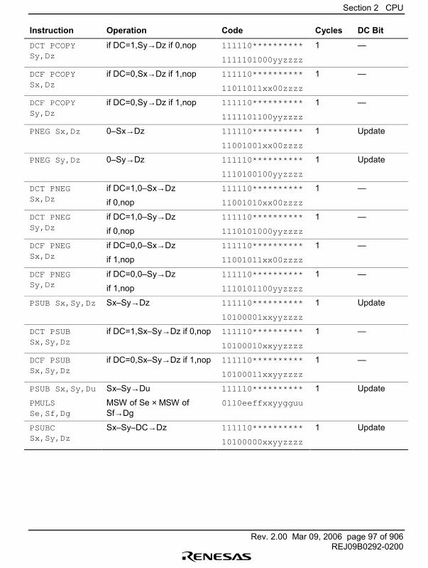
Section 2 CPU
Rev. 2.00 Mar 09, 2006 page 97 of 906REJ09B0292-0200
Instruction Operation Code Cycles DC Bit
DCT PCOPYSy,Dz
if DC=1,Sy→Dz if 0,nop 111110**********
1111101000yyzzzz
1 �
DCF PCOPYSx,Dz
if DC=0,Sx→Dz if 1,nop 111110**********
11011011xx00zzzz
1 �
DCF PCOPYSy,Dz
if DC=0,Sy→Dz if 1,nop 111110**********
1111101100yyzzzz
1 �
PNEG Sx,Dz 0�Sx→Dz 111110**********
11001001xx00zzzz
1 Update
PNEG Sy,Dz 0�Sy→Dz 111110**********
1110100100yyzzzz
1 Update
DCT PNEGSx,Dz
if DC=1,0�Sx→Dz
if 0,nop
111110**********
11001010xx00zzzz
1 �
DCT PNEGSy,Dz
if DC=1,0�Sy→Dz
if 0,nop
111110**********
1110101000yyzzzz
1 �
DCF PNEGSx,Dz
if DC=0,0�Sx→Dz
if 1,nop
111110**********
11001011xx00zzzz
1 �
DCF PNEGSy,Dz
if DC=0,0�Sy→Dz
if 1,nop
111110**********
1110101100yyzzzz
1 �
PSUB Sx,Sy,Dz Sx�Sy→Dz 111110**********
10100001xxyyzzzz
1 Update
DCT PSUBSx,Sy,Dz
if DC=1,Sx�Sy→Dz if 0,nop 111110**********
10100010xxyyzzzz
1 �
DCF PSUBSx,Sy,Dz
if DC=0,Sx�Sy→Dz if 1,nop 111110**********
10100011xxyyzzzz
1 �
PSUB Sx,Sy,Du
PMULSSe,Sf,Dg
Sx�Sy→Du
MSW of Se × MSW ofSf→Dg
111110**********
0110eeffxxyygguu
1 Update
PSUBCSx,Sy,Dz
Sx�Sy�DC→Dz 111110**********
10100000xxyyzzzz
1 Update
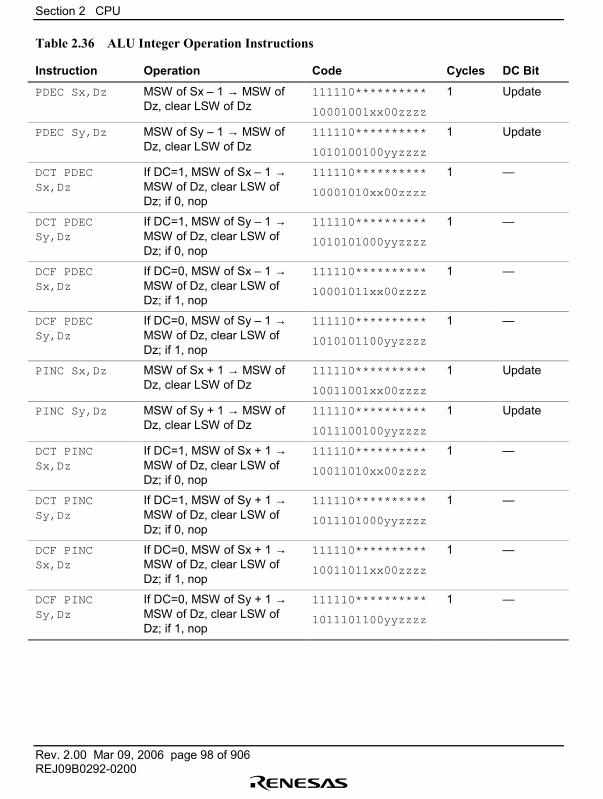
Section 2 CPU
Rev. 2.00 Mar 09, 2006 page 98 of 906REJ09B0292-0200
Table 2.36 ALU Integer Operation Instructions
Instruction Operation Code Cycles DC Bit
PDEC Sx,Dz MSW of Sx � 1 → MSW ofDz, clear LSW of Dz
111110**********
10001001xx00zzzz
1 Update
PDEC Sy,Dz MSW of Sy � 1 → MSW ofDz, clear LSW of Dz
111110**********
1010100100yyzzzz
1 Update
DCT PDECSx,Dz
If DC=1, MSW of Sx � 1 →MSW of Dz, clear LSW ofDz; if 0, nop
111110**********
10001010xx00zzzz
1 �
DCT PDECSy,Dz
If DC=1, MSW of Sy � 1 →MSW of Dz, clear LSW ofDz; if 0, nop
111110**********
1010101000yyzzzz
1 �
DCF PDECSx,Dz
If DC=0, MSW of Sx � 1 →MSW of Dz, clear LSW ofDz; if 1, nop
111110**********
10001011xx00zzzz
1 �
DCF PDECSy,Dz
If DC=0, MSW of Sy � 1 →MSW of Dz, clear LSW ofDz; if 1, nop
111110**********
1010101100yyzzzz
1 �
PINC Sx,Dz MSW of Sx + 1 → MSW ofDz, clear LSW of Dz
111110**********
10011001xx00zzzz
1 Update
PINC Sy,Dz MSW of Sy + 1 → MSW ofDz, clear LSW of Dz
111110**********
1011100100yyzzzz
1 Update
DCT PINCSx,Dz
If DC=1, MSW of Sx + 1 →MSW of Dz, clear LSW ofDz; if 0, nop
111110**********
10011010xx00zzzz
1 �
DCT PINCSy,Dz
If DC=1, MSW of Sy + 1 →MSW of Dz, clear LSW ofDz; if 0, nop
111110**********
1011101000yyzzzz
1 �
DCF PINCSx,Dz
If DC=0, MSW of Sx + 1 →MSW of Dz, clear LSW ofDz; if 1, nop
111110**********
10011011xx00zzzz
1 �
DCF PINCSy,Dz
If DC=0, MSW of Sy + 1 →MSW of Dz, clear LSW ofDz; if 1, nop
111110**********
1011101100yyzzzz
1 �
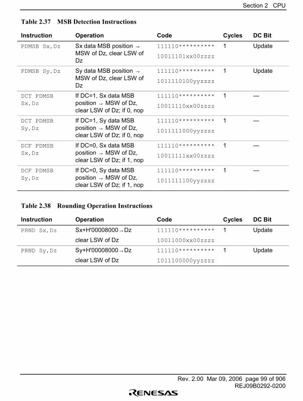
Section 2 CPU
Rev. 2.00 Mar 09, 2006 page 99 of 906REJ09B0292-0200
Table 2.37 MSB Detection Instructions
Instruction Operation Code Cycles DC Bit
PDMSB Sx,Dz Sx data MSB position →MSW of Dz, clear LSW ofDz
111110**********
10011101xx00zzzz
1 Update
PDMSB Sy,Dz Sy data MSB position →MSW of Dz, clear LSW ofDz
111110**********
1011110100yyzzzz
1 Update
DCT PDMSBSx,Dz
If DC=1, Sx data MSBposition → MSW of Dz,clear LSW of Dz; if 0, nop
111110**********
10011110xx00zzzz
1 �
DCT PDMSBSy,Dz
If DC=1, Sy data MSBposition → MSW of Dz,clear LSW of Dz; if 0, nop
111110**********
1011111000yyzzzz
1 �
DCF PDMSBSx,Dz
If DC=0, Sx data MSBposition → MSW of Dz,clear LSW of Dz; if 1, nop
111110**********
10011111xx00zzzz
1 �
DCF PDMSBSy,Dz
If DC=0, Sy data MSBposition → MSW of Dz,clear LSW of Dz; if 1, nop
111110**********
1011111100yyzzzz
1 �
Table 2.38 Rounding Operation Instructions
Instruction Operation Code Cycles DC Bit
PRND Sx,Dz Sx+H'00008000→Dz
clear LSW of Dz
111110**********
10011000xx00zzzz
1 Update
PRND Sy,Dz Sy+H'00008000→Dz
clear LSW of Dz
111110**********
1011100000yyzzzz
1 Update
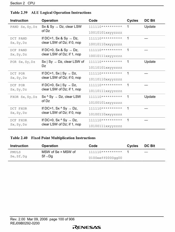
Section 2 CPU
Rev. 2.00 Mar 09, 2006 page 100 of 906REJ09B0292-0200
Table 2.39 ALU Logical Operation Instructions
Instruction Operation Code Cycles DC Bit
PAND Sx,Sy,Dz Sx & Sy → Dz, clear LSWof Dz
111110**********
10010101xxyyzzzz
1 Update
DCT PANDSx,Sy,Dz
If DC=1, Sx & Sy → Dz,clear LSW of Dz; if 0, nop
111110**********
10010110xxyyzzzz
1 �
DCF PANDSx,Sy,Dz
If DC=0, Sx & Sy → Dz,clear LSW of Dz; if 1, nop
111110**********
10010111xxyyzzzz
1 �
POR Sx,Sy,Dz Sx | Sy → Dz, clear LSW ofDz
111110**********
10110101xxyyzzzz
1 Update
DCT PORSx,Sy,Dz
If DC=1, Sx | Sy → Dz,clear LSW of Dz; if 0, nop
111110**********
10110110xxyyzzzz
1 �
DCF PORSx,Sy,Dz
If DC=0, Sx | Sy → Dz,clear LSW of Dz; if 1, nop
111110**********
10110111xxyyzzzz
1 �
PXOR Sx,Sy,Dz Sx ^ Sy → Dz, clear LSWof Dz
111110**********
10100101xxyyzzzz
1 Update
DCT PXORSx,Sy,Dz
If DC=1, Sx ^ Sy → Dz,clear LSW of Dz; if 0, nop
111110**********
10100110xxyyzzzz
1 �
DCF PXORSx,Sy,Dz
If DC=0, Sx ^ Sy → Dz,clear LSW of Dz; if 1, nop
111110**********
10100111xxyyzzzz
1 �
Table 2.40 Fixed Point Multiplication Instructions
Instruction Operation Code Cycles DC Bit
PMULSSe,Sf,Dg
MSW of Se × MSW ofSf→Dg
111110**********
0100eeff0000gg00
1 �
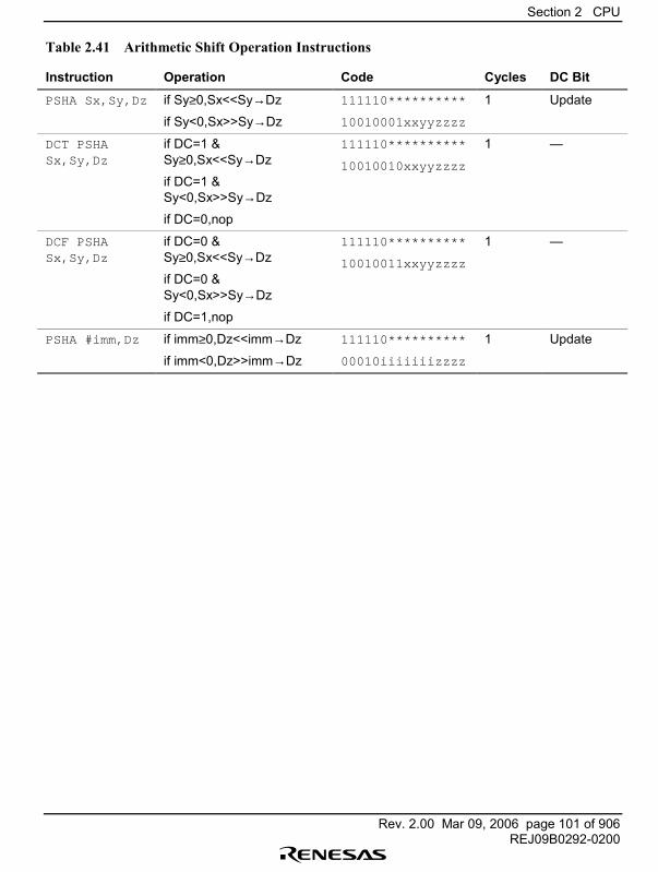
Section 2 CPU
Rev. 2.00 Mar 09, 2006 page 101 of 906REJ09B0292-0200
Table 2.41 Arithmetic Shift Operation Instructions
Instruction Operation Code Cycles DC Bit
PSHA Sx,Sy,Dz if Sy≥0,Sx<<Sy→Dz
if Sy<0,Sx>>Sy→Dz
111110**********
10010001xxyyzzzz
1 Update
DCT PSHASx,Sy,Dz
if DC=1 &Sy≥0,Sx<<Sy→Dz
if DC=1 &Sy<0,Sx>>Sy→Dz
if DC=0,nop
111110**********
10010010xxyyzzzz
1 �
DCF PSHASx,Sy,Dz
if DC=0 &Sy≥0,Sx<<Sy→Dz
if DC=0 &Sy<0,Sx>>Sy→Dz
if DC=1,nop
111110**********
10010011xxyyzzzz
1 �
PSHA #imm,Dz if imm≥0,Dz<<imm→Dz
if imm<0,Dz>>imm→Dz
111110**********
00010iiiiiiizzzz
1 Update
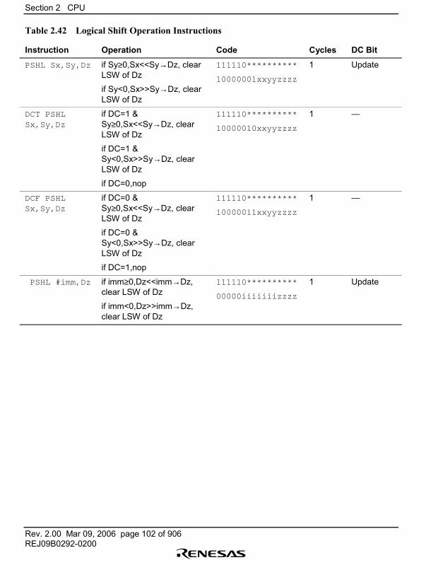
Section 2 CPU
Rev. 2.00 Mar 09, 2006 page 102 of 906REJ09B0292-0200
Table 2.42 Logical Shift Operation Instructions
Instruction Operation Code Cycles DC Bit
PSHL Sx,Sy,Dz if Sy≥0,Sx<<Sy→Dz, clearLSW of Dz
if Sy<0,Sx>>Sy→Dz, clearLSW of Dz
111110**********
10000001xxyyzzzz
1 Update
DCT PSHLSx,Sy,Dz
if DC=1 &Sy≥0,Sx<<Sy→Dz, clearLSW of Dz
if DC=1 &Sy<0,Sx>>Sy→Dz, clearLSW of Dz
if DC=0,nop
111110**********
10000010xxyyzzzz
1 �
DCF PSHLSx,Sy,Dz
if DC=0 &Sy≥0,Sx<<Sy→Dz, clearLSW of Dz
if DC=0 &Sy<0,Sx>>Sy→Dz, clearLSW of Dz
if DC=1,nop
111110**********
10000011xxyyzzzz
1 �
PSHL #imm,Dz if imm≥0,Dz<<imm→Dz,clear LSW of Dz
if imm<0,Dz>>imm→Dz,clear LSW of Dz
111110**********
00000iiiiiiizzzz
1 Update
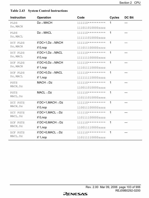
Section 2 CPU
Rev. 2.00 Mar 09, 2006 page 103 of 906REJ09B0292-0200
Table 2.43 System Control Instructions
Instruction Operation Code Cycles DC Bit
PLDSDz,MACH
Dz→MACH 111110**********
111011010000zzzz
1 �
PLDSDz,MACL
Dz→MACL 111110**********
111111010000zzzz
1 �
DCT PLDSDz,MACH
if DC=1,Dz→MACH
if 0,nop
111110**********
111011100000zzzz
1 �
DCT PLDSDz,MACL
if DC=1,Dz→MACL
if 0,nop
111110**********
111111100000zzzz
1 �
DCF PLDSDz,MACH
if DC=0,Dz→MACH
if 1,nop
111110**********
111011110000zzzz
1 �
DCF PLDSDz,MACL
if DC=0,Dz→MACL
if 1,nop
111110**********
111111110000zzzz
1 �
PSTSMACH,Dz
MACH→Dz 111110**********
110011010000zzzz
1 �
PSTSMACL,Dz
MACL→Dz 111110**********
110111010000zzzz
1 �
DCT PSTSMACH,Dz
if DC=1,MACH→Dz
if 0,nop
111110**********
110011100000zzzz
1 �
DCT PSTSMACL,Dz
if DC=1,MACL→Dz
if 0,nop
111110**********
110111100000zzzz
1 �
DCF PSTSMACH,Dz
if DC=0,MACH→Dz
if 1,nop
111110**********
110011110000zzzz
1 �
DCF PSTSMACL,Dz
if DC=0,MACL→Dz
if 1,nop
111110**********
110111110000zzzz
1 �
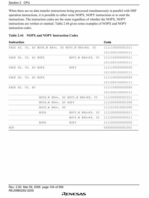
Section 2 CPU
Rev. 2.00 Mar 09, 2006 page 104 of 906REJ09B0292-0200
When there are no data transfer instructions being processed simultaneously in parallel with DSPoperation instructions, it is possible to either write NOPX, NOPY instructions or to omit theinstructions. The instruction codes are the same regardless of whether the NOPX, NOPYinstructions are written or omitted. Table 2.44 gives some examples of NOPX and NOPYinstruction codes.
Table 2.44 NOPX and NOPY Instruction Codes
Instruction Code
PADD X0, Y0, A0 MOVX.W @R4+, X0 MOVY.W @R6+R9, Y0 1111100000001011
1011000100000111
PADD X0, Y0, A0 NOPX MOVY.W @R6+R9, Y0 1111100000000011
1011000100000111
PADD X0, Y0, A0 NOPX NOPY 1111100000000000
1011000100000111
PADD X0, Y0, A0 NOPX 1111100000000000
1011000100000111
PADD X0, Y0, A0 1111100000000000
1011000100000111
MOVX.W @R4+, X0 MOVY.W @R6+R9, Y0 1111000000001011
MOVX.W @R4+, X0 NOPY 1111000000001000
MOVS.W @R4+, X0 1111010010001000
NOPX MOVY.W @R6+R9, Y0 1111000000000011
MOVY.W @R6+R9, Y0 1111000000000011
NOPX NOPY 1111000000000000
NOP 0000000000001001
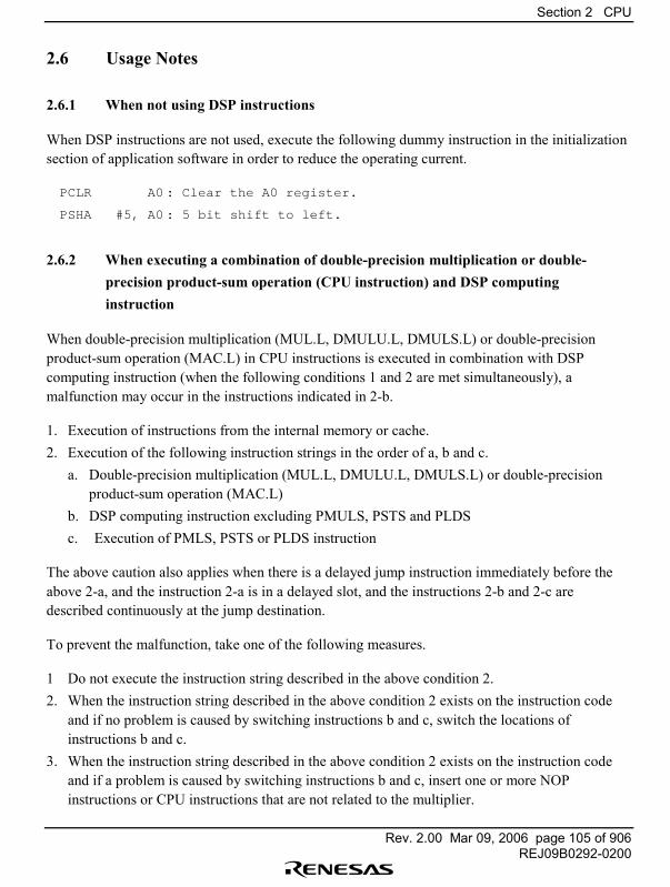
Section 2 CPU
Rev. 2.00 Mar 09, 2006 page 105 of 906REJ09B0292-0200
2.6 Usage Notes
2.6.1 When not using DSP instructions
When DSP instructions are not used, execute the following dummy instruction in the initializationsection of application software in order to reduce the operating current.
PCLR A0 : Clear the A0 register.
PSHA #5, A0 : 5 bit shift to left.
2.6.2 When executing a combination of double-precision multiplication or double-precision product-sum operation (CPU instruction) and DSP computinginstruction
When double-precision multiplication (MUL.L, DMULU.L, DMULS.L) or double-precisionproduct-sum operation (MAC.L) in CPU instructions is executed in combination with DSPcomputing instruction (when the following conditions 1 and 2 are met simultaneously), amalfunction may occur in the instructions indicated in 2-b.
1. Execution of instructions from the internal memory or cache.2. Execution of the following instruction strings in the order of a, b and c.
a. Double-precision multiplication (MUL.L, DMULU.L, DMULS.L) or double-precisionproduct-sum operation (MAC.L)
b. DSP computing instruction excluding PMULS, PSTS and PLDSc. Execution of PMLS, PSTS or PLDS instruction
The above caution also applies when there is a delayed jump instruction immediately before theabove 2-a, and the instruction 2-a is in a delayed slot, and the instructions 2-b and 2-c aredescribed continuously at the jump destination.
To prevent the malfunction, take one of the following measures.
1 Do not execute the instruction string described in the above condition 2.2. When the instruction string described in the above condition 2 exists on the instruction code
and if no problem is caused by switching instructions b and c, switch the locations ofinstructions b and c.
3. When the instruction string described in the above condition 2 exists on the instruction codeand if a problem is caused by switching instructions b and c, insert one or more NOPinstructions or CPU instructions that are not related to the multiplier.
Section 2 CPU
Rev. 2.00 Mar 09, 2006 page 106 of 906REJ09B0292-0200
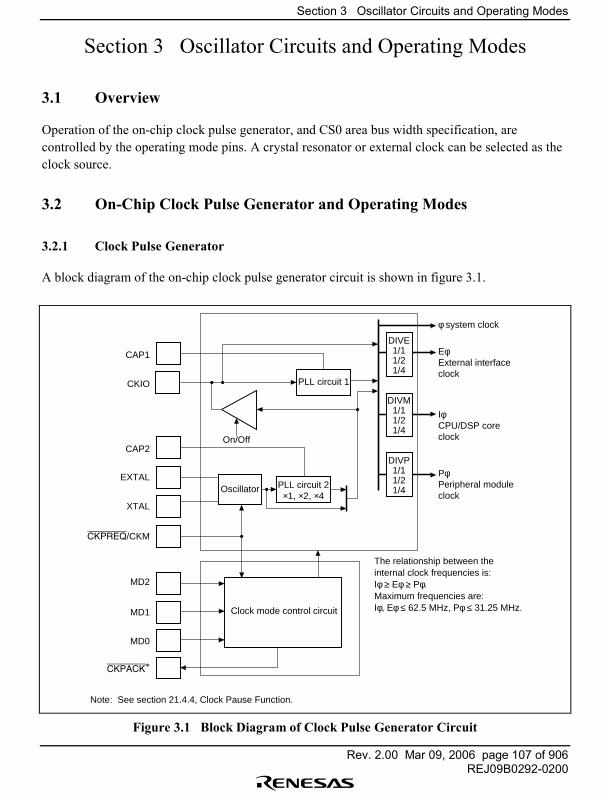
Section 3 Oscillator Circuits and Operating Modes
Rev. 2.00 Mar 09, 2006 page 107 of 906REJ09B0292-0200
Section 3 Oscillator Circuits and Operating Modes
3.1 Overview
Operation of the on-chip clock pulse generator, and CS0 area bus width specification, arecontrolled by the operating mode pins. A crystal resonator or external clock can be selected as theclock source.
3.2 On-Chip Clock Pulse Generator and Operating Modes
3.2.1 Clock Pulse Generator
A block diagram of the on-chip clock pulse generator circuit is shown in figure 3.1.
CAP1
CKIO
MD2
MD0
MD1
CKPACK*
Oscillator
On/Off
PLL circuit 1
PLL circuit 2×1, ×2, ×4
CAP2
EXTAL
XTAL
CKPREQ/CKM
Clock mode control circuit
DIVP1/11/21/4
Note: See section 21.4.4, Clock Pause Function.
Eφ External interface clock
IφCPU/DSP core clock
PφPeripheral module clock
The relationship between the internal clock frequencies is: Iφ ≥ Eφ ≥ Pφ.Maximum frequencies are: Iφ, Eφ ≤ 62.5 MHz, Pφ ≤ 31.25 MHz.
DIVE1/11/21/4
DIVM1/11/21/4
φ system clock
Figure 3.1 Block Diagram of Clock Pulse Generator Circuit
Section 3 Oscillator Circuits and Operating Modes
Rev. 2.00 Mar 09, 2006 page 108 of 906REJ09B0292-0200
Pin Configuration: Table 3.1 lists the functions relating to the pins relating to the oscillatorcircuit.
Table 3.1 Pin Configuration
Pin Name I/O Function
CKIO I/O External clock input pin or internal clock output pin
XTAL O Connects to the crystal resonator
EXTAL I Connects to the crystal resonator or to the external clock input whenusing PLL circuit 2
CAP1 I Connects to capacitance for operating PLL circuit 1
CAP2 I Connects to capacitance for operating PLL circuit 2
MD0 I The level applied to these pins specifies the clock mode
MD1 I
MD2 I
CKPREQ/CKM I Used as the clock pause request pin, or specifies operation of the crystalresonator
CKPACK O Clock pause function
PLL Circuit 1: PLL circuit 1 eliminates phase differences between external clocks and clockssupplied internally within the chip. In high-speed operation, the phase difference between thereference clocks and operating clocks in the chip directly affects the interface margin withperipheral devices. On-chip PLL circuit 1 is provided to eliminate this effect.
PLL Circuit 2: PLL circuit 2 either leaves unchanged, doubles, or quadruples the frequency ofclocks provided from the crystal resonator or the EXTAL pin external clock input for the chipoperating frequency. The frequency modification register sets the clock frequency multiplicationfactor.
Section 3 Oscillator Circuits and Operating Modes
Rev. 2.00 Mar 09, 2006 page 109 of 906REJ09B0292-0200
3.2.2 Clock Operating Mode Settings
Table 3.2 lists the functions and operation of clock modes 0 to 6.
Table 3.2 Operating Modes
Clock Mode Function/Operation Clock Source
0 PLL circuits 1 and 2 operate. A clock is output with the samephase (with the same frequency as Eφ) as the internal clocks(Iφ, Eφ, Pφ) from the CKIO pin
PLL circuits 1 and 2 can be switched between the operatingand halted states by means of control bits in the frequencymodification register (FMR). The CKIO pin can also be placedin the high-impedance state
Normally, mode 0 should be used.
Crystal resonator/external clock input
1 PLL circuits 1 and 2 operate. A clock (with the samefrequency as Eφ) 1/4 φ cycle in advance of the chip's internalsystem clock φ is output from the CKIO pin.
PLL circuits 1 and 2 can be switched between the operatingand halted states by means of control bits in the frequencymodification register (FMR). The CKIO pin can also be placedin the high-impedance state. However, clock phase shifting isnot performed when PLL circuit 1 is halted.
Normally, mode 0 should be used.
2 Only PLL circuit 2 operates. The clock from PLL circuit 2 isoutput from the CKIO pin (having the same frequency as theEφ). As PLL circuit 1 does not operate, phases are notmatched in this mode
PLL circuit 2 can be switched between the operating andhalted states by means of a control bit in the frequencymodification register (FMR). The CKIO pin can also be placedin the high-impedance state
3 Only PLL circuit 2 operates. The CKIO pin is high-impedance
PLL circuit 2 can be switched between the operating andhalted states by means of a control bit in the frequencymodification register (FMR)
4 Only PLL circuit 1 operates. Operate PLL circuit 1 whenoperating with synchronization of the phases of the clockinput from the CKIO pin and the internal clocks (Iφ, Eφ, Pφ).PLL circuit 2 does not operate in this mode
PLL circuit 1 can be switched between the operating andhalted states by means of a control bit in the frequencymodification register (FMR)
External clock input
Section 3 Oscillator Circuits and Operating Modes
Rev. 2.00 Mar 09, 2006 page 110 of 906REJ09B0292-0200
Clock Mode Function/Operation Clock Source
5 Only PLL circuit 1 operates. Operate PLL circuit 1 whenoperating with a 1/4 φ cycle lag of the clock input from theCKIO pin and the internal clocks (Iφ, Eφ, Pφ) with respect tosystem clock φ. PLL circuit 2 does not operate in this mode
PLL circuit 1 can be switched between the operating andhalted states by means of control bits in the frequencymodification register (FMR). However, clock phase shifting isnot performed when PLL circuit 1 is halted.
Normally, mode 4 should be used.
External clock input
6 PLL circuits 1 and 2 do not operate. Set this mode when aclock having a frequency equal to that of clocks the clockinput from the CKIO pin is used
The internal clock frequency can be changed in each clock mode (see section 3.2.5, OperatingFrequency Selection by Register).
In clock modes 4 to 6, the frequency of the clock input from the CKIO pin can be changed, or theclock can be stopped (see section 21.4.4, Clock Pause Function).
Table 3.3 lists the relationship between pins MD2 to MD0 and the clock operating mode. Do notswitch the MD2�MD0 pins while they are operating. Switching will cause operating errors.
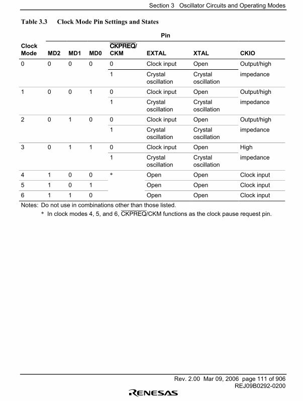
Section 3 Oscillator Circuits and Operating Modes
Rev. 2.00 Mar 09, 2006 page 111 of 906REJ09B0292-0200
Table 3.3 Clock Mode Pin Settings and States
Pin
ClockMode MD2 MD1 MD0
CKPREQCKPREQCKPREQCKPREQ/CKM EXTAL XTAL CKIO
0 0 0 0 0 Clock input Open Output/high
1 Crystaloscillation
Crystaloscillation
impedance
1 0 0 1 0 Clock input Open Output/high
1 Crystaloscillation
Crystaloscillation
impedance
2 0 1 0 0 Clock input Open Output/high
1 Crystaloscillation
Crystaloscillation
impedance
3 0 1 1 0 Clock input Open High
1 Crystaloscillation
Crystaloscillation
impedance
4 1 0 0 * Open Open Clock input
5 1 0 1 Open Open Clock input
6 1 1 0 Open Open Clock inputNotes: Do not use in combinations other than those listed.
* In clock modes 4, 5, and 6, CKPREQ/CKM functions as the clock pause request pin.
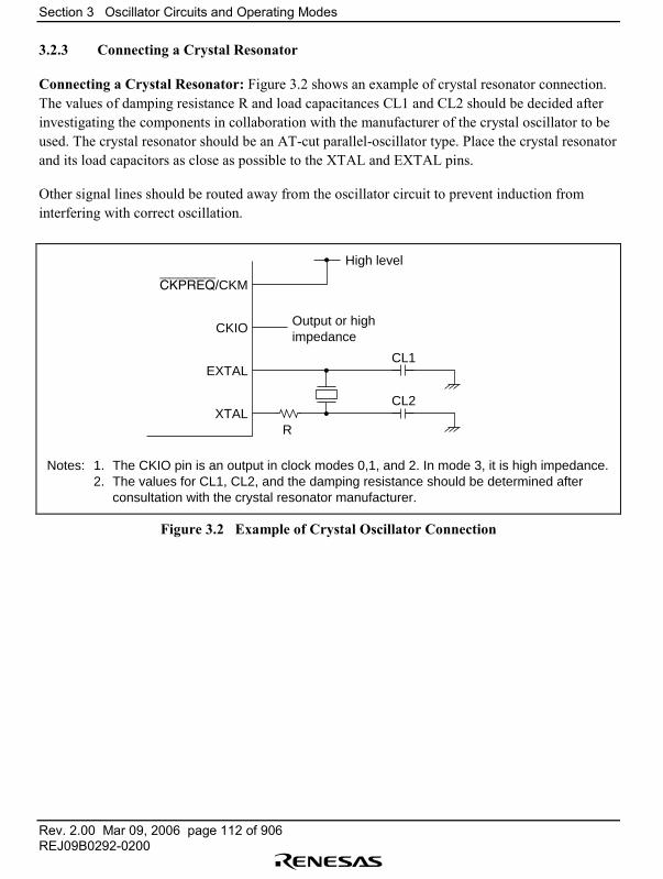
Section 3 Oscillator Circuits and Operating Modes
Rev. 2.00 Mar 09, 2006 page 112 of 906REJ09B0292-0200
3.2.3 Connecting a Crystal Resonator
Connecting a Crystal Resonator: Figure 3.2 shows an example of crystal resonator connection.The values of damping resistance R and load capacitances CL1 and CL2 should be decided afterinvestigating the components in collaboration with the manufacturer of the crystal oscillator to beused. The crystal resonator should be an AT-cut parallel-oscillator type. Place the crystal resonatorand its load capacitors as close as possible to the XTAL and EXTAL pins.
Other signal lines should be routed away from the oscillator circuit to prevent induction frominterfering with correct oscillation.
High level
Notes: 1. The CKIO pin is an output in clock modes 0,1, and 2. In mode 3, it is high impedance. 2. The values for CL1, CL2, and the damping resistance should be determined after consultation with the crystal resonator manufacturer.
CL1
R
CKPREQ/CKM
CKIO
EXTAL
XTAL
Output or highimpedance
CL2
Figure 3.2 Example of Crystal Oscillator Connection
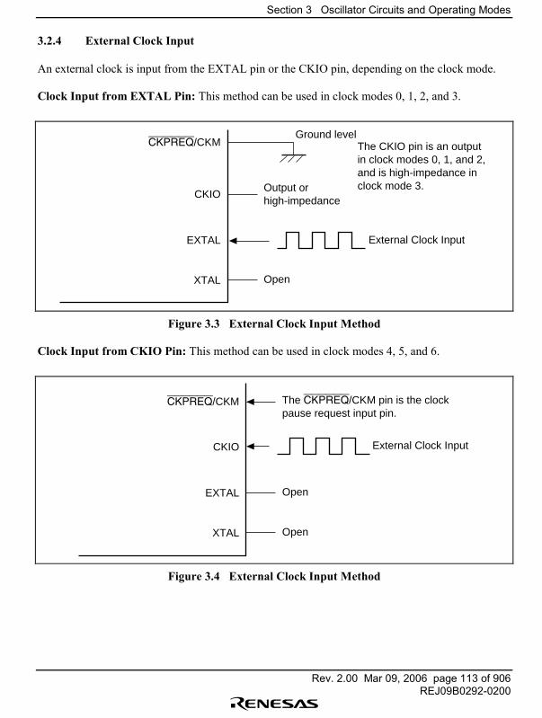
Section 3 Oscillator Circuits and Operating Modes
Rev. 2.00 Mar 09, 2006 page 113 of 906REJ09B0292-0200
3.2.4 External Clock Input
An external clock is input from the EXTAL pin or the CKIO pin, depending on the clock mode.
Clock Input from EXTAL Pin: This method can be used in clock modes 0, 1, 2, and 3.
CKPREQ/CKM
CKIO
EXTAL
XTAL
Output or high-impedance
The CKIO pin is an output in clock modes 0, 1, and 2, and is high-impedance in clock mode 3.
Open
External Clock Input
Ground level
Figure 3.3 External Clock Input Method
Clock Input from CKIO Pin: This method can be used in clock modes 4, 5, and 6.
CKPREQ/CKM
CKIO
EXTAL
XTAL Open
External Clock Input
Open
The CKPREQ/CKM pin is the clock pause request input pin.
Figure 3.4 External Clock Input Method
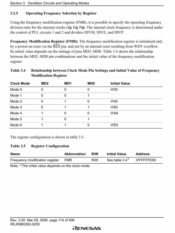
Section 3 Oscillator Circuits and Operating Modes
Rev. 2.00 Mar 09, 2006 page 114 of 906REJ09B0292-0200
3.2.5 Operating Frequency Selection by Register
Using the frequency modification register (FMR), it is possible to specify the operating frequencydivision ratio for the internal clocks (Iφ, Eφ, Pφ). The internal clock frequency is determined underthe control of PLL circuits 1 and 2 and dividers DIVM, DIVE, and DIVP.
Frequency Modification Register (FMR): The frequency modification register is initialized onlyby a power-on reset via the RES pin, and not by an internal reset resulting from WDT overflow.Its initial value depends on the settings of pins MD2�MD0. Table 3.4 shows the relationshipbetween the MD2�MD0 pin combinations and the initial value of the frequency modificationregister.
Table 3.4 Relationship between Clock Mode Pin Settings and Initial Value of FrequencyModification Register
Clock Mode MD2 MD1 MD0 Initial Value
Mode 0 0 0 0 H'00
Mode 1 0 0 1
Mode 2 0 1 0 H'40
Mode 3 0 1 1 H'60
Mode 4 1 0 0 H'A6
Mode 5 1 0 1
Mode 6 1 1 0 H'E0
The register configuration is shown in table 3.5.
Table 3.5 Register Configuration
Name Abbreviation R/W Initial Value Address
Frequency modification register FMR R/W See table 3.4* H'FFFFFE90Note: * The initial value depends on the clock mode.
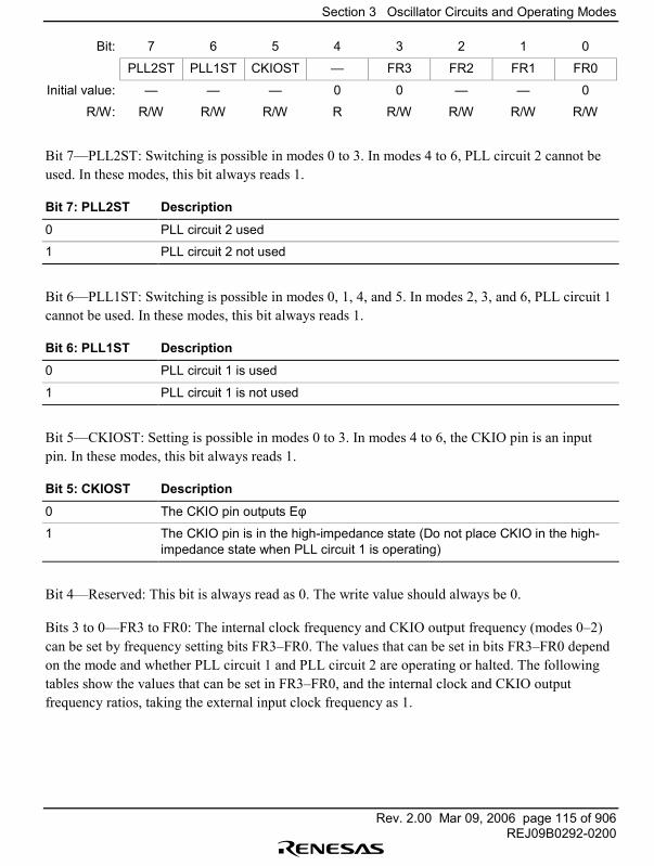
Section 3 Oscillator Circuits and Operating Modes
Rev. 2.00 Mar 09, 2006 page 115 of 906REJ09B0292-0200
Bit: 7 6 5 4 3 2 1 0
PLL2ST PLL1ST CKIOST � FR3 FR2 FR1 FR0
Initial value: � � � 0 0 � � 0
R/W: R/W R/W R/W R R/W R/W R/W R/W
Bit 7�PLL2ST: Switching is possible in modes 0 to 3. In modes 4 to 6, PLL circuit 2 cannot beused. In these modes, this bit always reads 1.
Bit 7: PLL2ST Description
0 PLL circuit 2 used
1 PLL circuit 2 not used
Bit 6�PLL1ST: Switching is possible in modes 0, 1, 4, and 5. In modes 2, 3, and 6, PLL circuit 1cannot be used. In these modes, this bit always reads 1.
Bit 6: PLL1ST Description
0 PLL circuit 1 is used
1 PLL circuit 1 is not used
Bit 5�CKIOST: Setting is possible in modes 0 to 3. In modes 4 to 6, the CKIO pin is an inputpin. In these modes, this bit always reads 1.
Bit 5: CKIOST Description
0 The CKIO pin outputs Eφ
1 The CKIO pin is in the high-impedance state (Do not place CKIO in the high-impedance state when PLL circuit 1 is operating)
Bit 4�Reserved: This bit is always read as 0. The write value should always be 0.
Bits 3 to 0�FR3 to FR0: The internal clock frequency and CKIO output frequency (modes 0�2)can be set by frequency setting bits FR3�FR0. The values that can be set in bits FR3�FR0 dependon the mode and whether PLL circuit 1 and PLL circuit 2 are operating or halted. The followingtables show the values that can be set in FR3�FR0, and the internal clock and CKIO outputfrequency ratios, taking the external input clock frequency as 1.
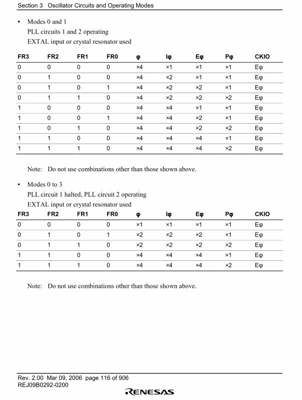
Section 3 Oscillator Circuits and Operating Modes
Rev. 2.00 Mar 09, 2006 page 116 of 906REJ09B0292-0200
• Modes 0 and 1PLL circuits 1 and 2 operatingEXTAL input or crystal resonator used
FR3 FR2 FR1 FR0 φφφφ Iφφφφ Eφφφφ Pφφφφ CKIO
0 0 0 0 ×4 ×1 ×1 ×1 Eφ
0 1 0 0 ×4 ×2 ×1 ×1 Eφ
0 1 0 1 ×4 ×2 ×2 ×1 Eφ
0 1 1 0 ×4 ×2 ×2 ×2 Eφ
1 0 0 0 ×4 ×4 ×1 ×1 Eφ
1 0 0 1 ×4 ×4 ×2 ×1 Eφ
1 0 1 0 ×4 ×4 ×2 ×2 Eφ
1 1 0 0 ×4 ×4 ×4 ×1 Eφ
1 1 1 0 ×4 ×4 ×4 ×2 Eφ
Note: Do not use combinations other than those shown above.
• Modes 0 to 3PLL circuit 1 halted, PLL circuit 2 operatingEXTAL input or crystal resonator used
FR3 FR2 FR1 FR0 φφφφ Iφφφφ Eφφφφ Pφφφφ CKIO
0 0 0 0 ×1 ×1 ×1 ×1 Eφ
0 1 0 1 ×2 ×2 ×2 ×1 Eφ
0 1 1 0 ×2 ×2 ×2 ×2 Eφ
1 1 0 0 ×4 ×4 ×4 ×1 Eφ
1 1 1 0 ×4 ×4 ×4 ×2 Eφ
Note: Do not use combinations other than those shown above.
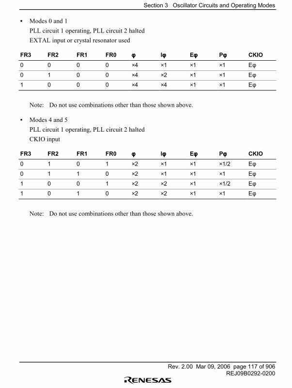
Section 3 Oscillator Circuits and Operating Modes
Rev. 2.00 Mar 09, 2006 page 117 of 906REJ09B0292-0200
• Modes 0 and 1PLL circuit 1 operating, PLL circuit 2 haltedEXTAL input or crystal resonator used
FR3 FR2 FR1 FR0 φφφφ Iφφφφ Eφφφφ Pφφφφ CKIO
0 0 0 0 ×4 ×1 ×1 ×1 Eφ
0 1 0 0 ×4 ×2 ×1 ×1 Eφ
1 0 0 0 ×4 ×4 ×1 ×1 Eφ
Note: Do not use combinations other than those shown above.
• Modes 4 and 5PLL circuit 1 operating, PLL circuit 2 haltedCKIO input
FR3 FR2 FR1 FR0 φφφφ Iφφφφ Eφφφφ Pφφφφ CKIO
0 1 0 1 ×2 ×1 ×1 ×1/2 Eφ
0 1 1 0 ×2 ×1 ×1 ×1 Eφ
1 0 0 1 ×2 ×2 ×1 ×1/2 Eφ
1 0 1 0 ×2 ×2 ×1 ×1 Eφ
Note: Do not use combinations other than those shown above.
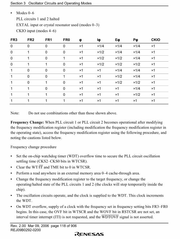
Section 3 Oscillator Circuits and Operating Modes
Rev. 2.00 Mar 09, 2006 page 118 of 906REJ09B0292-0200
• Modes 0�6PLL circuits 1 and 2 haltedEXTAL input or crystal resonator used (modes 0�3)CKIO input (modes 4�6)
FR3 FR2 FR1 FR0 φφφφ Iφφφφ Eφφφφ Pφφφφ CKIO
0 0 0 0 ×1 ×1/4 ×1/4 ×1/4 ×1
0 1 0 0 ×1 ×1/2 ×1/4 ×1/4 ×1
0 1 0 1 ×1 ×1/2 ×1/2 ×1/4 ×1
0 1 1 0 ×1 ×1/2 ×1/2 ×1/2 ×1
1 0 0 0 ×1 ×1 ×1/4 ×1/4 ×1
1 0 0 1 ×1 ×1 ×1/2 ×1/4 ×1
1 0 1 0 ×1 ×1 ×1/2 ×1/2 ×1
1 1 0 0 ×1 ×1 ×1 ×1/4 ×1
1 1 1 0 ×1 ×1 ×1 ×1/2 ×1
1 1 1 1 ×1 ×1 ×1 ×1 ×1
Note: Do not use combinations other than those shown above.
Frequency Change: When PLL circuit 1 or PLL circuit 2 becomes operational after modifyingthe frequency modification register (including modification the frequency modification register inthe operating state), access the frequency modification register using the following procedure, andnoting the cautions listed below.
Frequency change procedure
• Set the on-chip watchdog timer (WDT) overflow time to secure the PLL circuit oscillationsettling time (CKS2�CKS0 bits in WTCSR).
• Clear the WT/IT and TME bit to 0 in WTCSR.• Perform a read anywhere in an external memory area 0�4 cache-through area.• Change the frequency modification register to the target frequency, or change the
operating/halted state of the PLL circuits 1 and 2 (the clocks will stop temporarily inside thechip).
• The oscillation circuits operate, and the clock is supplied to the WDT. This clock incrementsthe WDT.
• On WDT overflow, supply of a clock with the frequency set in frequency setting bits FR3�FR0begins. In this case, the OVF bit in WTSCR and the WOVF bit in RSTCSR are not set, aninterval timer interrupt (ITI) is not requested, and the WDTOVF signal is not asserted.
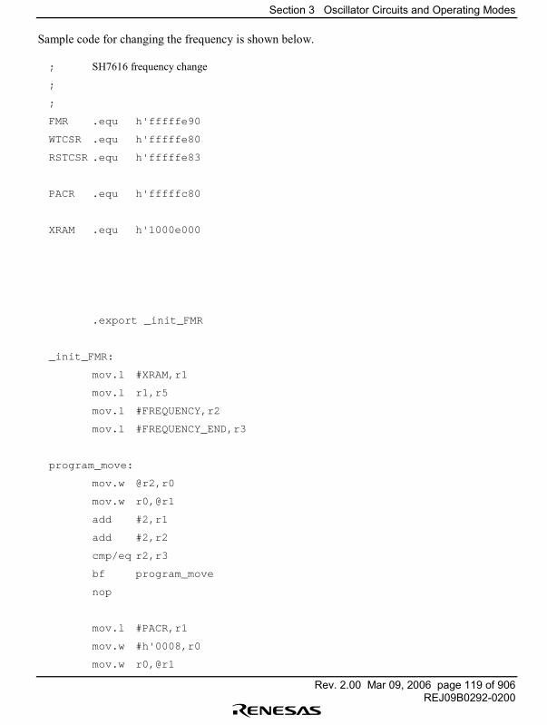
Section 3 Oscillator Circuits and Operating Modes
Rev. 2.00 Mar 09, 2006 page 119 of 906REJ09B0292-0200
Sample code for changing the frequency is shown below.
; SH7616 frequency change
;
;
FMR .equ h'fffffe90
WTCSR .equ h'fffffe80
RSTCSR .equ h'fffffe83
PACR .equ h'fffffc80
XRAM .equ h'1000e000
.export _init_FMR
_init_FMR:
mov.l #XRAM,r1
mov.l r1,r5
mov.l #FREQUENCY,r2
mov.l #FREQUENCY_END,r3
program_move:
mov.w @r2,r0
mov.w r0,@r1
add #2,r1
add #2,r2
cmp/eq r2,r3
bf program_move
nop
mov.l #PACR,r1
mov.w #h'0008,r0
mov.w r0,@r1
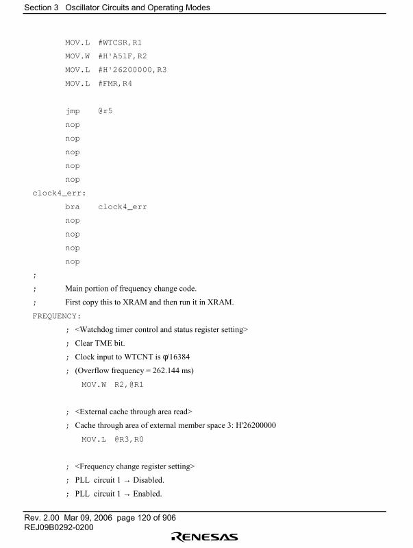
Section 3 Oscillator Circuits and Operating Modes
Rev. 2.00 Mar 09, 2006 page 120 of 906REJ09B0292-0200
MOV.L #WTCSR,R1
MOV.W #H'A51F,R2
MOV.L #H'26200000,R3
MOV.L #FMR,R4
jmp @r5
nop
nop
nop
nop
nop
clock4_err:
bra clock4_err
nop
nop
nop
nop
;
; Main portion of frequency change code.
; First copy this to XRAM and then run it in XRAM.
FREQUENCY:
; <Watchdog timer control and status register setting>
; Clear TME bit.
; Clock input to WTCNT is φ/16384
; (Overflow frequency = 262.144 ms)
MOV.W R2,@R1
; <External cache through area read>
; Cache through area of external member space 3: H'26200000
MOV.L @R3,R0
; <Frequency change register setting>
; PLL circuit 1 → Disabled.
; PLL circuit 1 → Enabled.

Section 3 Oscillator Circuits and Operating Modes
Rev. 2.00 Mar 09, 2006 page 121 of 906REJ09B0292-0200
; Iφ (×4) = 62.5 MHz, Eφ (×4) = 62.5 MHz,
; Pφ (×2) = 31.25 MHz, CKIO (Eφ) = 62.5 MHz,
; MOV #H'4E,R0
; PLL circuits 1 and 2 → Enabled.
; Iφ (×4) = 62.5 MHz, Eφ (×2) = 31.25 MHz,
; Pφ (×2 ) = 31.25 MHz, CKIO (Eφ) = 31.25 MHz,
MOV #H'0A,R0
; PLL circuits 1 and 2 → Enabled.
; Iφ (×4) = 62.5 MHz, Eφ (×1) = 15.625 MHz,
; Pφ (×1) = 15.625 MHz, CKIO (Eφ) = 15.625 MHz,
; MOV #H'08,R0
MOV.B R0,@R4
rts
nop
FREQUENCY_END:
NOP
.END
Cautions
• The read from the external memory space 0�4 cache-through area and the write to thefrequency modification register should be performed in on-chip X/Y memory. After readingfrom the external memory space 0�4 cache-through area, do not perform any write operationsin external memory spaces 0�4 until the write to the frequency modification register.
• When the write access to the frequency modification register is executed, the WDT startsautomatically.
• Do not turn off the CKIO output when PLL circuit 1 is in the operating state.• The CKIO output will be unstable until the PLL circuit stabilizes.• When a frequency is modified, halt the on-chip DMAC (E-DMAC and DMAC) operation
before the frequency modification.
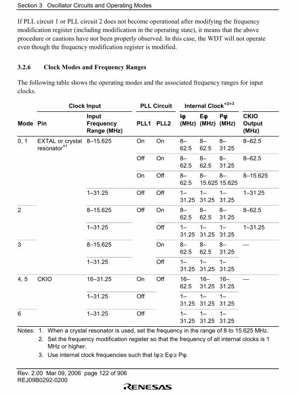
Section 3 Oscillator Circuits and Operating Modes
Rev. 2.00 Mar 09, 2006 page 122 of 906REJ09B0292-0200
If PLL circuit 1 or PLL circuit 2 does not become operational after modifying the frequencymodification register (including modification in the operating state), it means that the aboveprocedure or cautions have not been properly observed. In this case, the WDT will not operateeven though the frequency modification register is modified.
3.2.6 Clock Modes and Frequency Ranges
The following table shows the operating modes and the associated frequency ranges for inputclocks.
Clock Input PLL Circuit Internal Clock*2*3
Mode PinInputFrequencyRange (MHz)
PLL1 PLL2Iφφφφ(MHZ)
Eφφφφ(MHZ)
Pφφφφ(MHZ)
CKIOOutput(MHz)
0, 1 EXTAL or crystalresonator*1
8�15.625 On On 8�62.5
8�62.5
8�31.25
8�62.5
Off On 8�62.5
8�62.5
8�31.25
8�62.5
On Off 8�62.5
8�15.625
8�15.625
8�15.625
1�31.25 Off Off 1�31.25
1�31.25
1�31.25
1�31.25
2 8�15.625 Off On 8�62.5
8�62.5
8�31.25
8�62.5
1�31.25 Off 1�31.25
1�31.25
1�31.25
1�31.25
3 8�15.625 On 8�62.5
8�62.5
8�31.25
�
1�31.25 Off 1�31.25
1�31.25
1�31.25
4, 5 CKIO 16�31.25 On Off 16�62.5
16�31.25
16�31.25
�
1�31.25 Off 1�31.25
1�31.25
1�31.25
6 1�31.25 Off 1�31.25
1�31.25
1�31.25
Notes: 1. When a crystal resonator is used, set the frequency in the range of 8 to 15.625 MHz.2. Set the frequency modification register so that the frequency of all internal clocks is 1
MHz or higher.3. Use internal clock frequencies such that Iφ ≥ Eφ ≥ Pφ.
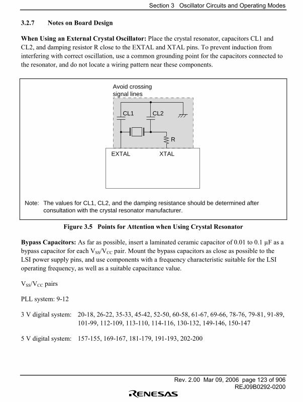
Section 3 Oscillator Circuits and Operating Modes
Rev. 2.00 Mar 09, 2006 page 123 of 906REJ09B0292-0200
3.2.7 Notes on Board Design
When Using an External Crystal Oscillator: Place the crystal resonator, capacitors CL1 andCL2, and damping resistor R close to the EXTAL and XTAL pins. To prevent induction frominterfering with correct oscillation, use a common grounding point for the capacitors connected tothe resonator, and do not locate a wiring pattern near these components.
Note: The values for CL1, CL2, and the damping resistance should be determined after consultation with the crystal resonator manufacturer.
XTALEXTAL
R
CL2CL1
Avoid crossing signal lines
Figure 3.5 Points for Attention when Using Crystal Resonator
Bypass Capacitors: As far as possible, insert a laminated ceramic capacitor of 0.01 to 0.1 µF as abypass capacitor for each VSS/VCC pair. Mount the bypass capacitors as close as possible to theLSI power supply pins, and use components with a frequency characteristic suitable for the LSIoperating frequency, as well as a suitable capacitance value.
VSS/VCC pairs
PLL system: 9-12
3 V digital system: 20-18, 26-22, 35-33, 45-42, 52-50, 60-58, 61-67, 69-66, 78-76, 79-81, 91-89,101-99, 112-109, 113-110, 114-116, 130-132, 149-146, 150-147
5 V digital system: 157-155, 169-167, 181-179, 191-193, 202-200
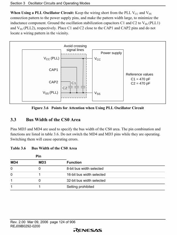
Section 3 Oscillator Circuits and Operating Modes
Rev. 2.00 Mar 09, 2006 page 124 of 906REJ09B0292-0200
When Using a PLL Oscillator Circuit: Keep the wiring short from the PLL VCC and VSS
connection pattern to the power supply pins, and make the pattern width large, to minimize theinductance component. Ground the oscillation stabilization capacitors C1 and C2 to VSS (PLL1)and VSS (PLL2), respectively. Place C1 and C2 close to the CAP1 and CAP2 pins and do notlocate a wiring pattern in the vicinity.
CAP1
VCC (PLL) VCC
C1 = 470 pFC2 = 470 pF
VSS
CAP2
VSS (PLL)
Avoid crossingsignal lines
Power supply
Reference values
C1C2
Figure 3.6 Points for Attention when Using PLL Oscillator Circuit
3.3 Bus Width of the CS0 Area
Pins MD3 and MD4 are used to specify the bus width of the CS0 area. The pin combination andfunctions are listed in table 3.6. Do not switch the MD4 and MD3 pins while they are operating.Switching them will cause operating errors.
Table 3.6 Bus Width of the CS0 Area
Pin
MD4 MD3 Function
0 0 8-bit bus width selected
0 1 16-bit bus width selected
1 0 32-bit bus width selected
1 1 Setting prohibited

Section 4 Exception Handling
Rev. 2.00 Mar 09, 2006 page 125 of 906REJ09B0292-0200
Section 4 Exception Handling
4.1 Overview
4.1.1 Types of Exception Handling and Priority Order
Exception handling is initiated by four sources: resets, address errors, interrupts, and instructions(table 4.1). When several exception sources occur simultaneously, they are accepted and processedaccording to the priority order shown in table 4.1.

Section 4 Exception Handling
Rev. 2.00 Mar 09, 2006 page 126 of 906REJ09B0292-0200
Table 4.1 Types of Exception Handling and Priority Order
Exception Source Priority
Reset Power-on reset High
Manual reset ↑
Address CPU address errorerror DMA address error (DMAC and E-DMAC)
Interrupt NMI
User break
User debug interface (H-UDI)
External interrupts (IRL1�IRL15, IRQ0�IRQ3 (set with IRL3, IRL2, IRL1,IRL0 pins))
On-chip peripheral modules Direct memory access controller (DMAC)
Watchdog timer (WDT)
Compare match interrupt (part of the busstate controller)
Ethernet controller (EtherC) and Ethernetcontroller direct memory access controller(E-DMAC)
16-bit free-running timer (FRT)
Serial communication interface with FIFO(SCIF)
16-bit timer pulse unit (TPU)
Serial I/O with FIFO (SIOF)
Serial I/O (SIO)
Instructions Trap instruction (TRAPA)
General illegal instructions (undefined code) ↓
Illegal slot instructions (undefined code placed directly following a delayedbranch instruction*1 or instructions that rewrite the PC*2)
Low
Notes: 1. Delayed branch instructions: JMP, JSR, BRA, BSR, RTS, RTE, BF/S, BT/S, BSRF,BRAF
2. Instructions that rewrite the PC: JMP, JSR, BRA, BSR, RTS, RTE, BT, BF, TRAPA,BF/S, BT/S, BSRF, BRAF

Section 4 Exception Handling
Rev. 2.00 Mar 09, 2006 page 127 of 906REJ09B0292-0200
4.1.2 Exception Handling Operations
Exception handling sources are detected, and exception handling started, according to the timingshown in table 4.2.
Table 4.2 Timing of Exception Source Detection and Start of Exception Handling
Exception Source Timing of Source Detection and Start of Handling
Reset Power-on reset Starts when the NMI pin is high and the RES pin changes fromlow to high
Manual reset Starts when the NMI pin is low and the RES pin changes fromlow to high
Address error Detected when instruction is decoded and starts when theprevious executing instruction finishes executing
Interrupts Detected when instruction is decoded and starts when theprevious executing instruction finishes executing
Instructions Trap instruction Starts from the execution of a TRAPA instruction
General illegalinstructions
Starts from the decoding of undefined code anytime except aftera delayed branch instruction (delay slot)
Illegal slotinstructions
Starts from the decoding of undefined code placed directlyfollowing a delayed branch instruction (delay slot) or of aninstruction that rewrites the PC
When exception handling starts, the CPU operates as follows:
1. Exception handling triggered by resetThe initial values of the program counter (PC) and stack pointer (SP) are fetched from theexception vector table (PC and SP are respectively addresses H'00000000 and H'00000004 fora power-on reset and addresses H'00000008 and H'0000000C addresses for a manual reset).See section 4.1.3, Exception Vector Table, for more information. 0 is then written to the vectorbase register (VBR) and 1111 is written to the interrupt mask bits (I3�I0) of the status register(SR). The program begins running from the PC address fetched from the exception vectortable.
2. Exception handling triggered by address errors, interrupts, and instructionsSR and PC are saved to the stack address indicated by R15. For interrupt exception handling,the interrupt priority level is written to the SR�s interrupt mask bits (I3�I0). For address errorand instruction exception handling, the I3�I0 bits are not affected. The start address is thenfetched from the exception vector table and the program begins running from that address.
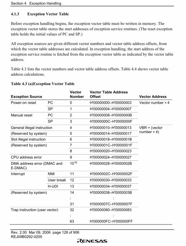
Section 4 Exception Handling
Rev. 2.00 Mar 09, 2006 page 128 of 906REJ09B0292-0200
4.1.3 Exception Vector Table
Before exception handling begins, the exception vector table must be written in memory. Theexception vector table stores the start addresses of exception service routines. (The reset exceptiontable holds the initial values of PC and SP.)
All exception sources are given different vector numbers and vector table address offsets, fromwhich the vector table addresses are calculated. In exception handling, the start address of theexception service routine is fetched from the exception vector table as indicated by the vector tableaddress.
Table 4.3 lists the vector numbers and vector table address offsets. Table 4.4 shows vector tableaddress calculations.
Table 4.3 (a)Exception Vector Table
Exception SourceVectorNumber
Vector Table Address Offset Vector Address
Power-on reset PC 0 H'00000000�H'00000003 Vector number × 4
SP 1 H'00000004�H'00000007
Manual reset PC 2 H'00000008�H'0000000B
SP 3 H'0000000C�H'0000000F
General illegal instruction 4 H'00000010�H'00000013 VBR + (vector(Reserved by system) 5 H'00000014�H'00000017 number × 4)
Slot illegal instruction 6 H'00000018�H'0000001B(Reserved by system) 7 H'0000001C�H'0000001F
8 H'00000020�H'00000023
CPU address error 9 H'00000024�H'00000027
DMA address error (DMAC andE-DMAC)
10*5 H'00000028�H'0000002B
Interrupt NMI 11 H'0000002C�H'0000002F
User break 12 H'00000030�H'00000033
H-UDI 13 H'00000034�H'00000037
(Reserved by system) 14:31
H'00000038�H'0000003B:
H'0000007C�H'0000007FTrap instruction (user vector) 32
:63
H'00000080�H'00000083:
H'000000FC�H'000000FF
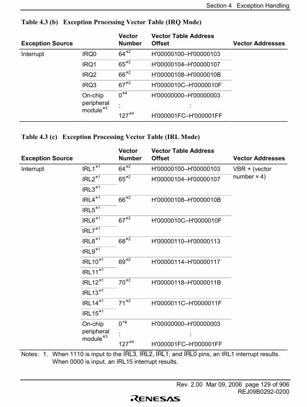
Section 4 Exception Handling
Rev. 2.00 Mar 09, 2006 page 129 of 906REJ09B0292-0200
Table 4.3 (b) Exception Processing Vector Table (IRQ Mode)
Exception SourceVectorNumber
Vector Table Address Offset Vector Addresses
Interrupt IRQ0 64*2 H'00000100�H'00000103
IRQ1 65*2 H'00000104�H'00000107
IRQ2 66*2 H'00000108�H'0000010B
IRQ3 67*2 H'0000010C�H'0000010F
On-chipperipheralmodule*3
0*4
:
127*4
H'00000000�H'00000003
:
H'000001FC�H'000001FF
Table 4.3 (c) Exception Processing Vector Table (IRL Mode)
Exception SourceVectorNumber
Vector Table Address Offset Vector Addresses
Interrupt IRL1*1 64*2 H'00000100�H'00000103 VBR + (vector
IRL2*1 65*2 H'00000104�H'00000107 number × 4)
IRL3*1
IRL4*1 66*2 H'00000108�H'0000010B
IRL5*1
IRL6*1 67*2 H'0000010C�H'0000010F
IRL7*1
IRL8*1 68*2 H'00000110�H'00000113
IRL9*1
IRL10*1 69*2 H'00000114�H'00000117
IRL11*1
IRL12*1 70*2 H'00000118�H'0000011B
IRL13*1
IRL14*1 71*2 H'0000011C�H'0000011F
IRL15*1
On-chipperipheralmodule*3
0*4
:
127*4
H'00000000�H'00000003
:
H'000001FC�H'000001FFNotes: 1. When 1110 is input to the IRL3, IRL2, IRL1, and IRL0 pins, an IRL1 interrupt results.
When 0000 is input, an IRL15 interrupt results.
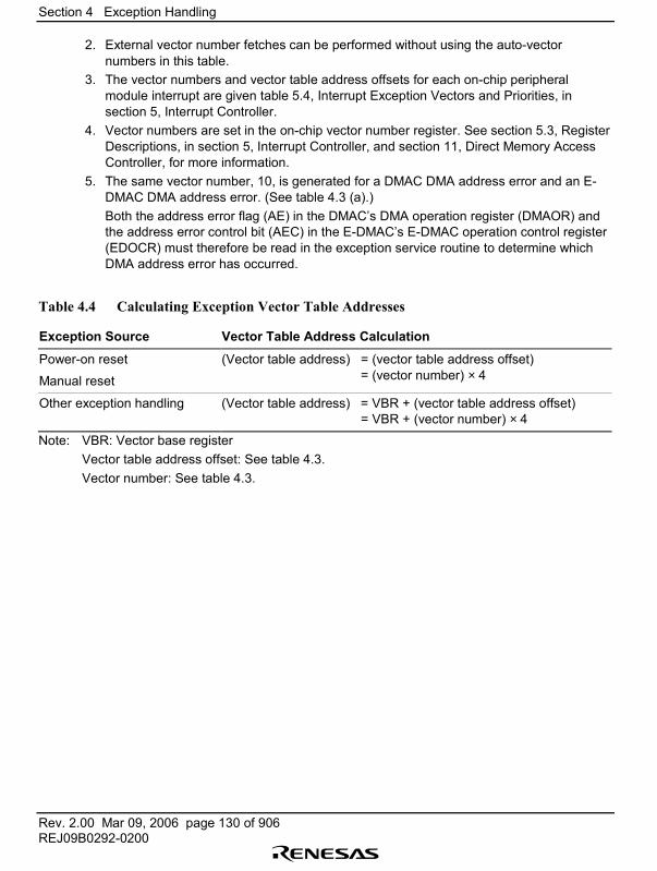
Section 4 Exception Handling
Rev. 2.00 Mar 09, 2006 page 130 of 906REJ09B0292-0200
2. External vector number fetches can be performed without using the auto-vectornumbers in this table.
3. The vector numbers and vector table address offsets for each on-chip peripheralmodule interrupt are given table 5.4, Interrupt Exception Vectors and Priorities, insection 5, Interrupt Controller.
4. Vector numbers are set in the on-chip vector number register. See section 5.3, RegisterDescriptions, in section 5, Interrupt Controller, and section 11, Direct Memory AccessController, for more information.
5. The same vector number, 10, is generated for a DMAC DMA address error and an E-DMAC DMA address error. (See table 4.3 (a).)Both the address error flag (AE) in the DMAC�s DMA operation register (DMAOR) andthe address error control bit (AEC) in the E-DMAC�s E-DMAC operation control register(EDOCR) must therefore be read in the exception service routine to determine whichDMA address error has occurred.
Table 4.4 Calculating Exception Vector Table Addresses
Exception Source Vector Table Address Calculation
Power-on reset
Manual reset
(Vector table address) = (vector table address offset)= (vector number) × 4
Other exception handling (Vector table address) = VBR + (vector table address offset)= VBR + (vector number) × 4
Note: VBR: Vector base registerVector table address offset: See table 4.3.Vector number: See table 4.3.
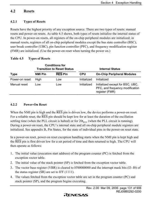
Section 4 Exception Handling
Rev. 2.00 Mar 09, 2006 page 131 of 906REJ09B0292-0200
4.2 Resets
4.2.1 Types of Resets
Resets have the highest priority of any exception source. There are two types of resets: manualresets and power-on resets. As table 4.5 shows, both types of resets initialize the internal status ofthe CPU. In power-on resets, all registers of the on-chip peripheral modules are initialized; inmanual resets, registers of all on-chip peripheral modules except the bus state controller (BSC),user break controller (UBC), pin function controller (PFC), and frequency modification register(FMR) are initialized. (Use the power-on reset when turning the power on.)
Table 4.5 Types of Resets
Conditions forTransition to Reset Status Internal Status
Type NMI Pin RESRESRESRES Pin CPU On-Chip Peripheral Modules
Power-on reset High Low Initialized Initialized
Manual reset Low Low Initialized Initialized except for BSC, UBC,PFC, and frequency modificationregister (FMR)
4.2.2 Power-On Reset
When the NMI pin is high and the RES pin is driven low, the device performs a power-on reset.For a reliable reset, the RES pin should be kept low for at least the duration of the oscillationsettling time (when the PLL circuit is halted) or for 20tpcyc (when the PLL circuit is running).During a power-on reset, the CPU�s internal state and all on-chip peripheral module registers areinitialized. See appendix B, Pin States, for the state of individual pins in the power-on reset state.
In a power-on reset, power-on reset exception handling starts when the NMI pin is kept high andthe RES pin is first driven low for a set period of time and then returned to high. The CPU willthen operate as follows:
1. The initial value (execution start address) of the program counter (PC) is fetched from theexception vector table.
2. The initial value of the stack pointer (SP) is fetched from the exception vector table.3. The vector base register (VBR) is cleared to H'00000000 and the interrupt mask bits (I3�I0) of
the status register (SR) are set to H'F (1111).4. The values fetched from the exception vector table are set in the program counter (PC) and
stack pointer (SP), and the program begins executing.
Section 4 Exception Handling
Rev. 2.00 Mar 09, 2006 page 132 of 906REJ09B0292-0200
4.2.3 Manual Reset
When the NMI pin is low and the RES pin is driven low, the device executes a manual reset. For areliable reset, the RES pin should be kept low for at least 20 clock cycles. During a manual reset,the CPU�s internal state is initialized. All on-chip peripheral module registers are initialized,except for the bus state controller (BSC), user break controller (UBC), and pin function controller(PFC) registers, and the frequency modification register (FMR). When the chip enters the manualreset state in the middle of a bus cycle, manual reset exception handling does not start until the buscycle has ended. Thus, manual resets do not abort bus cycles. See appendix B, Pin States, for thestate of individual pins in the manual reset state.
In a manual reset, manual reset exception handling starts when the NMI pin is kept low and theRES pin is first kept low for a set period of time and then returned to high. The CPU will thenoperate in the same way as for a power-on reset.
4.3 Address Errors
4.3.1 Sources of Address Errors
Address errors occur when instructions are fetched or data read or written, as shown in table 4.6.
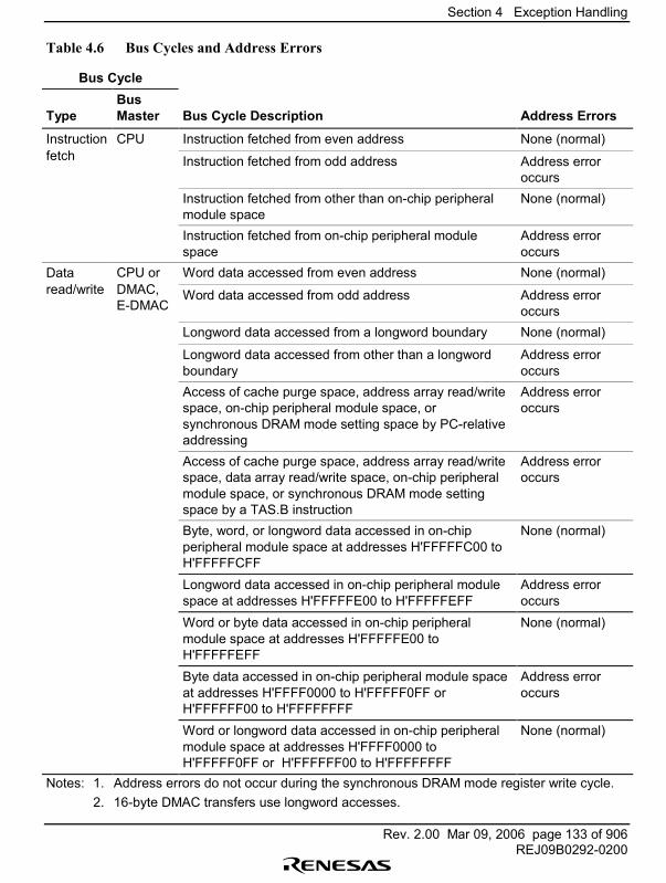
Section 4 Exception Handling
Rev. 2.00 Mar 09, 2006 page 133 of 906REJ09B0292-0200
Table 4.6 Bus Cycles and Address Errors
Bus Cycle
TypeBusMaster Bus Cycle Description Address Errors
Instruction CPU Instruction fetched from even address None (normal)fetch Instruction fetched from odd address Address error
occursInstruction fetched from other than on-chip peripheralmodule space
None (normal)
Instruction fetched from on-chip peripheral modulespace
Address erroroccurs
Data CPU or Word data accessed from even address None (normal)read/write DMAC,
E-DMACWord data accessed from odd address Address error
occursLongword data accessed from a longword boundary None (normal)
Longword data accessed from other than a longwordboundary
Address erroroccurs
Access of cache purge space, address array read/writespace, on-chip peripheral module space, orsynchronous DRAM mode setting space by PC-relativeaddressing
Address erroroccurs
Access of cache purge space, address array read/writespace, data array read/write space, on-chip peripheralmodule space, or synchronous DRAM mode settingspace by a TAS.B instruction
Address erroroccurs
Byte, word, or longword data accessed in on-chipperipheral module space at addresses H'FFFFFC00 toH'FFFFFCFF
None (normal)
Longword data accessed in on-chip peripheral modulespace at addresses H'FFFFFE00 to H'FFFFFEFF
Address erroroccurs
Word or byte data accessed in on-chip peripheralmodule space at addresses H'FFFFFE00 toH'FFFFFEFF
None (normal)
Byte data accessed in on-chip peripheral module spaceat addresses H'FFFF0000 to H'FFFFF0FF orH'FFFFFF00 to H'FFFFFFFF
Address erroroccurs
Word or longword data accessed in on-chip peripheralmodule space at addresses H'FFFF0000 toH'FFFFF0FF or H'FFFFFF00 to H'FFFFFFFF
None (normal)
Notes: 1. Address errors do not occur during the synchronous DRAM mode register write cycle.2. 16-byte DMAC transfers use longword accesses.
Section 4 Exception Handling
Rev. 2.00 Mar 09, 2006 page 134 of 906REJ09B0292-0200
4.3.2 Address Error Exception Handling
When an address error occurs, address error exception handling begins after the end of the buscycle in which the error occurred and completion of the executing instruction. The CPU operatesas follows:
1. The status register (SR) is saved to the stack.2. The program counter (PC) is saved to the stack. The PC value saved is the start address of the
instruction to be executed after the last instruction executed .3. The exception service routine start address is fetched from the exception vector table entry that
corresponds to the address error that occurred, and the program starts executing from thataddress. The jump that occurs is not a delayed branch.
Note: The same vector number, 10, is generated for a DMAC DMA address error and an E-DMAC DMA address error. (See table 4.3 (a).)
Both the address error flag (AE) in the DMAC�s DMA operation register (DMAOR) andthe address error control bit (AEC) in the E-DMAC�s E-DMAC operation control register(EDOCR) must therefore be read in the exception service routine to determine whichDMA address error has occurred.

Section 4 Exception Handling
Rev. 2.00 Mar 09, 2006 page 135 of 906REJ09B0292-0200
4.4 Interrupts
4.4.1 Interrupt Sources
Table 4.7 shows the sources that initiate interrupt exception handling. These are divided into NMI,user breaks, H-UDI, IRL, IRQ, and on-chip peripheral modules.
Table 4.7 Types of Interrupt Sources
Type Request Source Number of Sources
NMI NMI pin (external input) 1
User break User break controller (UBC) 1
H-UDI User debug interface (H-UDI) 1
IRL IRL1�IRL15 (external input) 15
IRQ IRQ0�IRQ3 (external input) 4
On-chip peripheral module Direct memory access controller (DMAC) 2
Ethernet controller (EtherC) and Ethernetcontroller direct memory access controller(E-DMAC)
1
16-bit free-running timer (FRT) 3
Watchdog timer (WDT) 1
Bus state controller (BSC) 1
Serial I/O with FIFO (SIOF) 4
Serial I/O (SIO) 4
Serial communication interface with FIFO(SCIF)
4
16-bit timer pulse unit (TPU) 13
Each interrupt source is allocated a different vector number and vector table address offset. Seetable 5.4, Interrupt Exception Vectors and Priority Order, in section 5, Interrupt Controller, formore information.
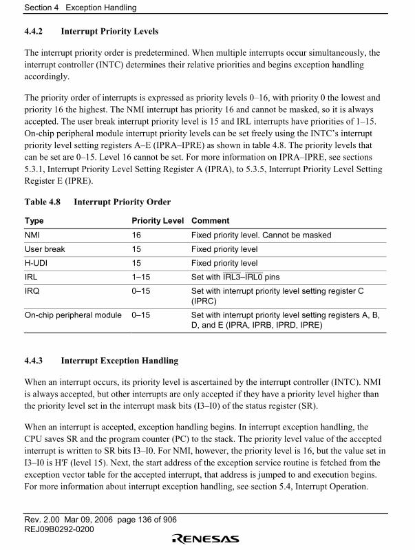
Section 4 Exception Handling
Rev. 2.00 Mar 09, 2006 page 136 of 906REJ09B0292-0200
4.4.2 Interrupt Priority Levels
The interrupt priority order is predetermined. When multiple interrupts occur simultaneously, theinterrupt controller (INTC) determines their relative priorities and begins exception handlingaccordingly.
The priority order of interrupts is expressed as priority levels 0�16, with priority 0 the lowest andpriority 16 the highest. The NMI interrupt has priority 16 and cannot be masked, so it is alwaysaccepted. The user break interrupt priority level is 15 and IRL interrupts have priorities of 1�15.On-chip peripheral module interrupt priority levels can be set freely using the INTC�s interruptpriority level setting registers A�E (IPRA�IPRE) as shown in table 4.8. The priority levels thatcan be set are 0�15. Level 16 cannot be set. For more information on IPRA�IPRE, see sections5.3.1, Interrupt Priority Level Setting Register A (IPRA), to 5.3.5, Interrupt Priority Level SettingRegister E (IPRE).
Table 4.8 Interrupt Priority Order
Type Priority Level Comment
NMI 16 Fixed priority level. Cannot be masked
User break 15 Fixed priority level
H-UDI 15 Fixed priority level
IRL 1�15 Set with IRL3�IRL0 pins
IRQ 0�15 Set with interrupt priority level setting register C(IPRC)
On-chip peripheral module 0�15 Set with interrupt priority level setting registers A, B,D, and E (IPRA, IPRB, IPRD, IPRE)
4.4.3 Interrupt Exception Handling
When an interrupt occurs, its priority level is ascertained by the interrupt controller (INTC). NMIis always accepted, but other interrupts are only accepted if they have a priority level higher thanthe priority level set in the interrupt mask bits (I3�I0) of the status register (SR).
When an interrupt is accepted, exception handling begins. In interrupt exception handling, theCPU saves SR and the program counter (PC) to the stack. The priority level value of the acceptedinterrupt is written to SR bits I3�I0. For NMI, however, the priority level is 16, but the value set inI3�I0 is H'F (level 15). Next, the start address of the exception service routine is fetched from theexception vector table for the accepted interrupt, that address is jumped to and execution begins.For more information about interrupt exception handling, see section 5.4, Interrupt Operation.
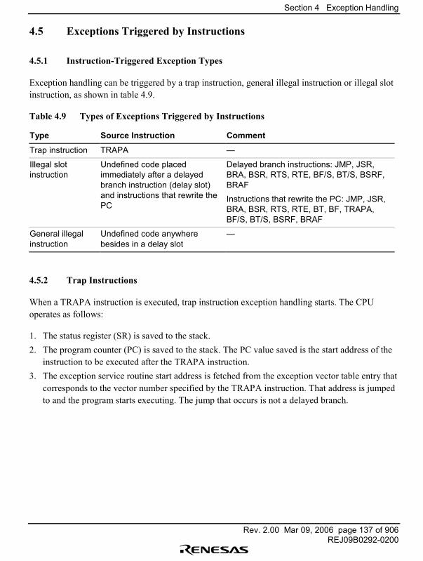
Section 4 Exception Handling
Rev. 2.00 Mar 09, 2006 page 137 of 906REJ09B0292-0200
4.5 Exceptions Triggered by Instructions
4.5.1 Instruction-Triggered Exception Types
Exception handling can be triggered by a trap instruction, general illegal instruction or illegal slotinstruction, as shown in table 4.9.
Table 4.9 Types of Exceptions Triggered by Instructions
Type Source Instruction Comment
Trap instruction TRAPA �
Illegal slotinstruction
Undefined code placedimmediately after a delayedbranch instruction (delay slot)and instructions that rewrite thePC
Delayed branch instructions: JMP, JSR,BRA, BSR, RTS, RTE, BF/S, BT/S, BSRF,BRAF
Instructions that rewrite the PC: JMP, JSR,BRA, BSR, RTS, RTE, BT, BF, TRAPA,BF/S, BT/S, BSRF, BRAF
General illegalinstruction
Undefined code anywherebesides in a delay slot
�
4.5.2 Trap Instructions
When a TRAPA instruction is executed, trap instruction exception handling starts. The CPUoperates as follows:
1. The status register (SR) is saved to the stack.2. The program counter (PC) is saved to the stack. The PC value saved is the start address of the
instruction to be executed after the TRAPA instruction.3. The exception service routine start address is fetched from the exception vector table entry that
corresponds to the vector number specified by the TRAPA instruction. That address is jumpedto and the program starts executing. The jump that occurs is not a delayed branch.
Section 4 Exception Handling
Rev. 2.00 Mar 09, 2006 page 138 of 906REJ09B0292-0200
4.5.3 Illegal Slot Instructions
An instruction placed immediately after a delayed branch instruction is said to be placed in a delayslot. If the instruction placed in the delay slot is undefined code, illegal slot exception handlingbegins when the undefined code is decoded. Illegal slot exception handling is also started when aninstruction that rewrites the program counter (PC) is placed in a delay slot. The exception handlingstarts when the instruction is decoded. The CPU handles an illegal slot instruction as follows:
1. The status register (SR) is saved to the stack.2. The program counter (PC) is saved to the stack. The PC value saved is the jump address of the
delayed branch instruction immediately before the undefined code or the instruction thatrewrites the PC.
3. The exception service routine start address is fetched from the exception vector table entry thatcorresponds to the exception that occurred. That address is jumped to and the program startsexecuting. The jump that occurs is not a delayed branch.
4.5.4 General Illegal Instructions
When undefined code placed anywhere other than immediately after a delayed branch instruction(i.e., in a delay slot) is decoded, general illegal instruction exception handling starts. The CPUhandles general illegal instructions in the same way as illegal slot instructions. Unlike processingof illegal slot instructions, however, the program counter value saved is the start address of theundefined code.
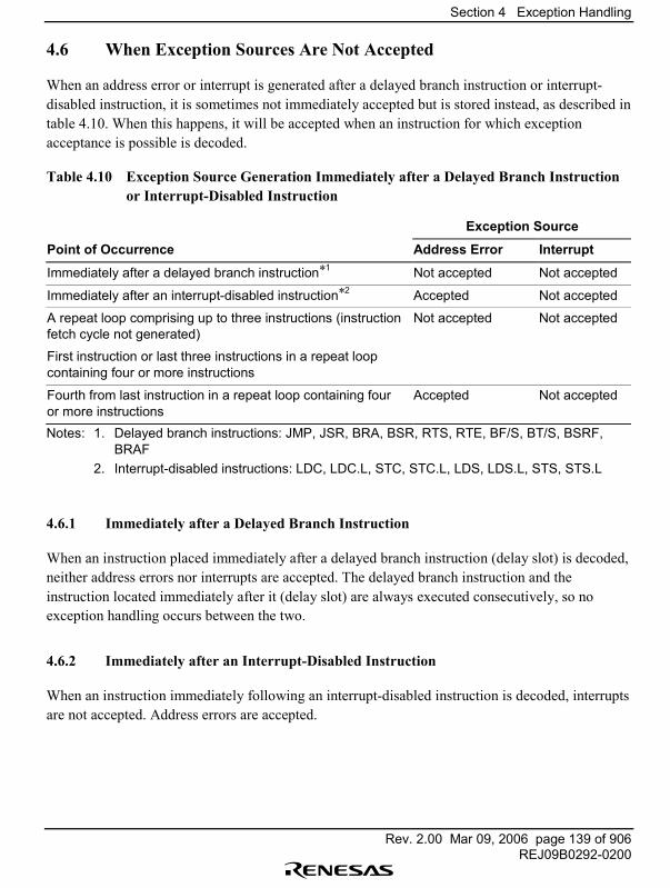
Section 4 Exception Handling
Rev. 2.00 Mar 09, 2006 page 139 of 906REJ09B0292-0200
4.6 When Exception Sources Are Not Accepted
When an address error or interrupt is generated after a delayed branch instruction or interrupt-disabled instruction, it is sometimes not immediately accepted but is stored instead, as described intable 4.10. When this happens, it will be accepted when an instruction for which exceptionacceptance is possible is decoded.
Table 4.10 Exception Source Generation Immediately after a Delayed Branch Instructionor Interrupt-Disabled Instruction
Exception Source
Point of Occurrence Address Error Interrupt
Immediately after a delayed branch instruction*1 Not accepted Not accepted
Immediately after an interrupt-disabled instruction*2 Accepted Not accepted
A repeat loop comprising up to three instructions (instructionfetch cycle not generated)
First instruction or last three instructions in a repeat loopcontaining four or more instructions
Not accepted Not accepted
Fourth from last instruction in a repeat loop containing fouror more instructions
Accepted Not accepted
Notes: 1. Delayed branch instructions: JMP, JSR, BRA, BSR, RTS, RTE, BF/S, BT/S, BSRF,BRAF
2. Interrupt-disabled instructions: LDC, LDC.L, STC, STC.L, LDS, LDS.L, STS, STS.L
4.6.1 Immediately after a Delayed Branch Instruction
When an instruction placed immediately after a delayed branch instruction (delay slot) is decoded,neither address errors nor interrupts are accepted. The delayed branch instruction and theinstruction located immediately after it (delay slot) are always executed consecutively, so noexception handling occurs between the two.
4.6.2 Immediately after an Interrupt-Disabled Instruction
When an instruction immediately following an interrupt-disabled instruction is decoded, interruptsare not accepted. Address errors are accepted.
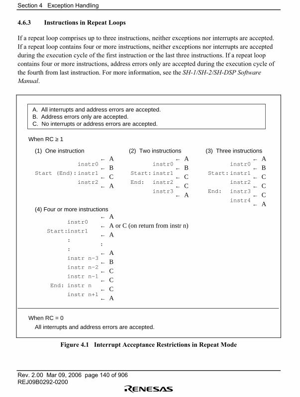
Section 4 Exception Handling
Rev. 2.00 Mar 09, 2006 page 140 of 906REJ09B0292-0200
4.6.3 Instructions in Repeat Loops
If a repeat loop comprises up to three instructions, neither exceptions nor interrupts are accepted.If a repeat loop contains four or more instructions, neither exceptions nor interrupts are acceptedduring the execution cycle of the first instruction or the last three instructions. If a repeat loopcontains four or more instructions, address errors only are accepted during the execution cycle ofthe fourth from last instruction. For more information, see the SH-1/SH-2/SH-DSP SoftwareManual.
A. All interrupts and address errors are accepted.B. Address errors only are accepted.C. No interrupts or address errors are accepted.
When RC ≥ 1
When RC = 0
All interrupts and address errors are accepted.
(1) One instruction← A
← B
← C
← A
instr0
instr1
instr2
Start (End):
(4) Four or more instructions← A
← A or C (on return from instr n)
← A
:
← A
← B
← C
← C
← C
← A
instr0
instr1
:
:
instr n-3
instr n-2
instr n-1
instr n
instr n+1
Start:
End:
(2) Two instructions← A
← B
← C
← C
← A
instr0
instr1
instr2
instr3
Start:
End:
(3) Three instructions← A
← B
← C
← C
← C
← A
instr0
instr1
instr2
instr3
instr4
Start:
End:
Figure 4.1 Interrupt Acceptance Restrictions in Repeat Mode
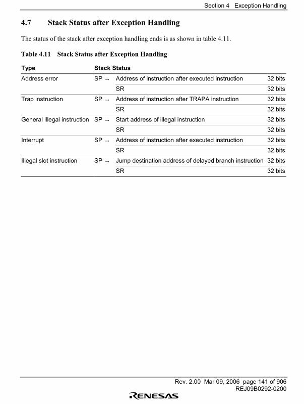
Section 4 Exception Handling
Rev. 2.00 Mar 09, 2006 page 141 of 906REJ09B0292-0200
4.7 Stack Status after Exception Handling
The status of the stack after exception handling ends is as shown in table 4.11.
Table 4.11 Stack Status after Exception Handling
Type Stack Status
Address error SP → Address of instruction after executed instruction 32 bits
SR 32 bits
Trap instruction SP → Address of instruction after TRAPA instruction 32 bits
SR 32 bits
General illegal instruction SP → Start address of illegal instruction 32 bits
SR 32 bits
Interrupt SP → Address of instruction after executed instruction 32 bits
SR 32 bits
Illegal slot instruction SP → Jump destination address of delayed branch instruction 32 bits
SR 32 bits
Section 4 Exception Handling
Rev. 2.00 Mar 09, 2006 page 142 of 906REJ09B0292-0200
4.8 Usage Notes
4.8.1 Value of Stack Pointer (SP)
The value of the stack pointer must always be a multiple of four, otherwise an address error willoccur when the stack is accessed during exception handling.
4.8.2 Value of Vector Base Register (VBR)
The value of the vector base register must always be a multiple of four, otherwise an address errorwill occur when the vector table is accessed during exception handling.
4.8.3 Address Errors Caused by Stacking of Address Error Exception Handling
If the stack pointer value is not a multiple of four, an address error will occur during stacking ofthe exception handling (interrupts, etc.). Address error exception handling will begin after theoriginal exception handling ends, but address errors will continue to occur. To ensure that addresserror exception handling does not go into an endless loop, no address errors are accepted at thatpoint. This allows program control to be shifted to the address error exception service routine andenables error handling to be carried out.
When an address error occurs during exception handling stacking, the stacking bus cycle (write) isexecuted. In stacking of the status register (SR) and program counter (PC), the SP is decrementedby 4 for both, so the value of SP will not be a multiple of four after the stacking either. Theaddress value output during stacking is the SP value, so the address where the error occurred isitself output. This means that the write data stacked will be undefined.
4.8.4 Manual Reset during Register Access
Do not initiate a manual reset during access of a bus state controller (BSC), user break controller(UBC), or pin function controller (PFC) register, or the frequency modification register (FMR),otherwise a write error may result.
Section 5 Interrupt Controller (INTC)
Rev. 2.00 Mar 09, 2006 page 143 of 906REJ09B0292-0200
Section 5 Interrupt Controller (INTC)
5.1 Overview
The interrupt controller (INTC) ascertains the priority order of interrupt sources and controlsinterrupt requests to the CPU. The INTC has registers for setting the priority of each interruptwhich allow the user to set the order of priority in which interrupt requests are handled.
5.1.1 Features
The INTC has the following features:
• Sixteen interrupt priority levels can be setBy setting the five interrupt priority registers, the priorities of on-chip peripheral moduleinterrupts can be selected at 16 levels for different request sources.
• Vector numbers for on-chip peripheral module interrupt can be setBy setting the 24 vector number setting registers, the vector numbers of on-chip peripheralmodule interrupts can be set to values from 0 to 127 for different request sources.
• The IRL interrupt vector number setting method can be selected: Either of two modes can beselected by a register setting: auto-vector mode in which vector numbers are determinedinternally, and external vector mode in which vector numbers are set externally.
• IRQ interrupt settings can be made (low level, rising-, falling-, or both-edge detection)
5.1.2 Block Diagram
Figure 5.1 shows a block diagram of the INTC.
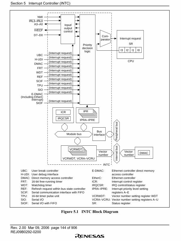
Section 5 Interrupt Controller (INTC)
Rev. 2.00 Mar 09, 2006 page 144 of 906REJ09B0292-0200
CPU
SR
Interrupt requestCom-
parator
Prioritydecision
logic(Interrupt request)
(Interrupt request)
(Interrupt request)
(Interrupt request)
(Interrupt request)
(Interrupt request)
(Interrupt request)
(Interrupt request)
(Interrupt request)
(Interrupt request)
(Interrupt request)
ICR
IRQCSR IPRA–IPRE
VCRWDT, VCRA–VCRU
Module busBus
interface
Inte
rnal
bus
I3 I2 I1 I0
INTC
NMIIRL3–IRL0
A3–A0
IVECF
D7–D0
UBC
H-UDI
DMAC
FRT
WDT
REF
SCIF
TPU
SIO
E-DMAC
Input/outputcontrol
Vector number
Vector number
DMAC
Per
iphe
ral b
us
VCRWDT
IPR
UBC: User break controllerH-UDI: User debug interfaceDMAC: Direct memory access controllerFRT: 16-bit free-running timerWDT: Watchdog timerREF: Refresh request within bus state controllerSCIF: Serial communication interface with FIFOTPU: 16-bit timer pulse unitSIO: Serial I/OSIOF: Serial I/O with FIFO
E-DMAC: Ethernet controller direct memory access controllerEtherC: Ethernet controller ICR: Interrupt control registerIRQCSR: IRQ control/status registerIPRA–IPRE: Interrupt priority level setting registers A–EVCRWDT: Vector number setting register WDTVCRA–VCRU: Vector number setting registers A–USR: Status register
(Including EtherCinterrupt)
SIOF
Figure 5.1 INTC Block Diagram
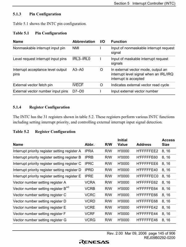
Section 5 Interrupt Controller (INTC)
Rev. 2.00 Mar 09, 2006 page 145 of 906REJ09B0292-0200
5.1.3 Pin Configuration
Table 5.1 shows the INTC pin configuration.
Table 5.1 Pin Configuration
Name Abbreviation I/O Function
Nonmaskable interrupt input pin NMI I Input of nonmaskable interrupt requestsignal
Level request interrupt input pins IRL3�IRL0 I Input of maskable interrupt requestsignals
Interrupt acceptance level outputpins
A3�A0 O In external vector mode, output aninterrupt level signal when an IRL/IRQinterrupt is accepted
External vector fetch pin IVECF O Indicates external vector read cycle
External vector number input pins D7�D0 I Input external vector number
5.1.4 Register Configuration
The INTC has the 31 registers shown in table 5.2. These registers perform various INTC functionsincluding setting interrupt priority, and controlling external interrupt input signal detection.
Table 5.2 Register Configuration
Name Abbr. R/WInitialValue Address
AccessSize
Interrupt priority register setting register A IPRA R/W H'0000 H'FFFFFEE2 8, 16
Interrupt priority register setting register B IPRB R/W H'0000 H'FFFFFE60 8, 16
Interrupt priority register setting register C IPRC R/W H'0000 H'FFFFFEE6 8, 16
Interrupt priority register setting register D IPRD R/W H'0000 H'FFFFFE40 8, 16
Interrupt priority register setting register E IPRE R/W H'0000 H'FFFFFEC0 8, 16
Vector number setting register A VCRA R/W H'0000 H'FFFFFE62 8, 16
Vector number setting register B*3 VCRB R/W H'0000 H'FFFFFE64 8, 16
Vector number setting register C VCRC R/W H'0000 H'FFFFFE66 8, 16
Vector number setting register D VCRD R/W H'0000 H'FFFFFE68 8, 16
Vector number setting register E VCRE R/W H'0000 H'FFFFFE42 8, 16
Vector number setting register F VCRF R/W H'0000 H'FFFFFE44 8, 16
Vector number setting register G VCRG R/W H'0000 H'FFFFFE46 8, 16
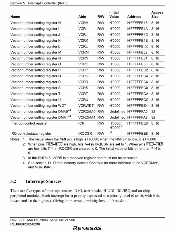
Section 5 Interrupt Controller (INTC)
Rev. 2.00 Mar 09, 2006 page 146 of 906REJ09B0292-0200
Name Abbr. R/WInitialValue Address
AccessSize
Vector number setting register H VCRH R/W H'0000 H'FFFFFE48 8, 16
Vector number setting register I VCRI R/W H'0000 H'FFFFFE4A 8, 16
Vector number setting register J VCRJ R/W H'0000 H'FFFFFE4C 8, 16
Vector number setting register K VCRK R/W H'0000 H'FFFFFE4E 8, 16
Vector number setting register L VCRL R/W H'0000 H'FFFFFE 50 8, 16
Vector number setting register M VCRM R/W H'0000 H'FFFFFE52 8, 16
Vector number setting register N VCRN R/W H'0000 H'FFFFFE54 8, 16
Vector number setting register O VCRO R/W H'0000 H'FFFFFE56 8, 16
Vector number setting register P VCRP R/W H'0000 H'FFFFFEC2 8, 16
Vector number setting register Q VCRQ R/W H'0000 H'FFFFFEC4 8, 16
Vector number setting register R VCRR R/W H'0000 H'FFFFFEC6 8, 16
Vector number setting register S VCRS R/W H'0000 H'FFFFFEC8 8, 16
Vector number setting register T VCRT R/W H'0000 H'FFFFFECA 8, 16
Vector number setting register U VCRU R/W H'0000 H'FFFFFECC 8, 16
Vector number setting register WDT VCRWDT R/W H'0000 H'FFFFFEE4 8, 16
Vector number setting register DMA0*4 VCRDMA0 R/W Undefined H'FFFFFFA0 32
Vector number setting register DMA1*4 VCRDMA1 R/W Undefined H'FFFFFFA8 32
Interrupt control register ICR R/W H'8000/H'0000*1
H'FFFFFEE0 8, 16
IRQ control/status register IRQCSR R/W *2 H'FFFFFEE8 8, 16Notes: 1. The value when the NMI pin is high is H'8000; when the NMI pin is low, it is H'0000.
2. When pins IRL3�IRL0 are high, bits 7�4 in IRQCSR are set to 1. When pins IRL3�IRL0are low, bits 7�4 in IRQCSR are cleared to 0. The initial value of bits other than 7�4 is0.
3. In the SH7616, VCRB is a reserved register and must not be accessed.4. See section 11, Direct Memory Access Controlle for more information on VCRDMA0,
and VCRDMA1.
5.2 Interrupt Sources
There are five types of interrupt sources: NMI, user breaks, H-UDI, IRL/IRQ and on-chipperipheral modules. Each interrupt has a priority expressed as a priority level (0 to 16, with 0 thelowest and 16 the highest). Giving an interrupt a priority level of 0 masks it.
Section 5 Interrupt Controller (INTC)
Rev. 2.00 Mar 09, 2006 page 147 of 906REJ09B0292-0200
5.2.1 NMI Interrupt
The NMI interrupt has priority 16 and is always accepted. Input at the NMI pin is detected byedge. Use the NMI edge select bit (NMIE) in the interrupt control register (ICR) to select eitherthe rising or falling edge. NMI interrupt exception handling sets the interrupt mask level bits (I3�I0) in the status register (SR) to level 15.
5.2.2 User Break Interrupt
A user break interrupt has priority level 15 and occurs when the break condition set in the userbreak controller (UBC) is satisfied. User break interrupt exception handling sets the interrupt masklevel bits (I3�I0) in the status register (SR) to level 15. For more information about the user breakinterrupt, see section 6, User Break Controller.
5.2.3 H-UDI Interrupt
The H-UDI interrupt has a priority level of 15, and is generated when an H-UDI interruptinstruction is serially input. H-UDI interrupt exception processing sets the interrupt mask bits (I3�I0) in the status register (SR) to level 15. See section 18, User Debug Interface, for details of theH-UDI interrupt.
5.2.4 IRL Interrupts
IRL interrupts are requested by input from pins IRL3�IRL0. Fifteen interrupts, IRL15�IRL1, canbe input externally via pins IRL3�IRL0. The priority levels of interrupts IRL15�IRL0 are 15�1,respectively, and their vector numbers are 71�64. Set the vector numbers with the interrupt vectormode select (VECMD) bit of the interrupt control register (ICR) to enable external input. Externalinput of vector numbers consists of vector numbers 0�127 from the external vector input pins(D7�D0). When an external vector is used, 0 is input to D7. Internal vectors are called auto-vectors and vectors input externally are called external vectors. Table 5.3 lists IRL priority levelsand auto vector numbers.
When an IRL interrupt is accepted in external vector mode, the IRL interrupt level is output fromthe interrupt acceptance level output pins (A3�A0). The external vector fetch pin (IVECF) is alsoasserted. The external vector number is read from pins D7�D0 at this time.
IRL interrupt exception processing sets the interrupt mask level bits (I3 to I0) in the status register(SR) to the priority level value of the IRL interrupt that was accepted.
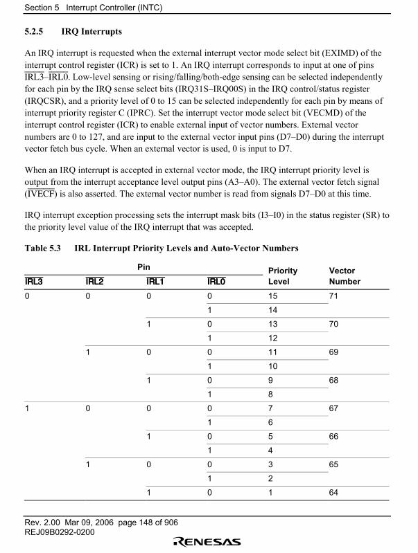
Section 5 Interrupt Controller (INTC)
Rev. 2.00 Mar 09, 2006 page 148 of 906REJ09B0292-0200
5.2.5 IRQ Interrupts
An IRQ interrupt is requested when the external interrupt vector mode select bit (EXIMD) of theinterrupt control register (ICR) is set to 1. An IRQ interrupt corresponds to input at one of pinsIRL3�IRL0. Low-level sensing or rising/falling/both-edge sensing can be selected independentlyfor each pin by the IRQ sense select bits (IRQ31S�IRQ00S) in the IRQ control/status register(IRQCSR), and a priority level of 0 to 15 can be selected independently for each pin by means ofinterrupt priority register C (IPRC). Set the interrupt vector mode select bit (VECMD) of theinterrupt control register (ICR) to enable external input of vector numbers. External vectornumbers are 0 to 127, and are input to the external vector input pins (D7�D0) during the interruptvector fetch bus cycle. When an external vector is used, 0 is input to D7.
When an IRQ interrupt is accepted in external vector mode, the IRQ interrupt priority level isoutput from the interrupt acceptance level output pins (A3�A0). The external vector fetch signal(IVECF) is also asserted. The external vector number is read from signals D7�D0 at this time.
IRQ interrupt exception processing sets the interrupt mask bits (I3�I0) in the status register (SR) tothe priority level value of the IRQ interrupt that was accepted.
Table 5.3 IRL Interrupt Priority Levels and Auto-Vector Numbers
Pin Priority VectorIRL3IRL3IRL3IRL3 IRL2IRL2IRL2IRL2 IRL1IRL1IRL1IRL1 IRL0IRL0IRL0IRL0 Level Number
0 0 0 0 15 71
1 14
1 0 13 70
1 12
1 0 0 11 69
1 10
1 0 9 68
1 8
1 0 0 0 7 67
1 6
1 0 5 66
1 4
1 0 0 3 65
1 2
1 0 1 64
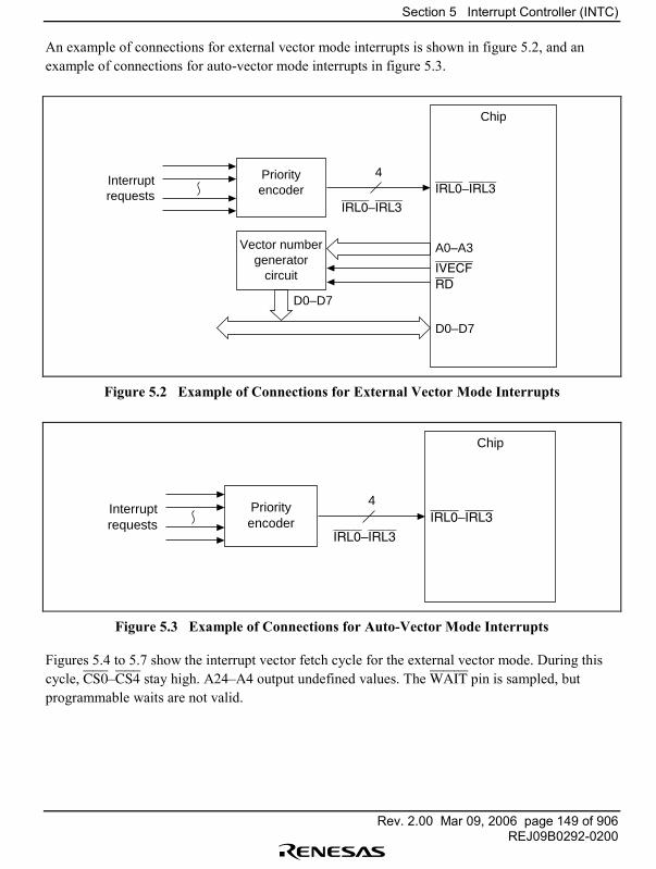
Section 5 Interrupt Controller (INTC)
Rev. 2.00 Mar 09, 2006 page 149 of 906REJ09B0292-0200
An example of connections for external vector mode interrupts is shown in figure 5.2, and anexample of connections for auto-vector mode interrupts in figure 5.3.
Chip
Priorityencoder
Interruptrequests
Vector numbergenerator
circuit
4IRL0–IRL3
IRL0–IRL3
D0–D7
A0–A3
IVECF
RD
D0–D7
Figure 5.2 Example of Connections for External Vector Mode Interrupts
Chip
Priorityencoder
Interruptrequests
4IRL0–IRL3
IRL0–IRL3
Figure 5.3 Example of Connections for Auto-Vector Mode Interrupts
Figures 5.4 to 5.7 show the interrupt vector fetch cycle for the external vector mode. During thiscycle, CS0�CS4 stay high. A24�A4 output undefined values. The WAIT pin is sampled, butprogrammable waits are not valid.
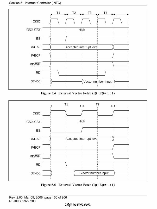
Section 5 Interrupt Controller (INTC)
Rev. 2.00 Mar 09, 2006 page 150 of 906REJ09B0292-0200
T1
CKIO
CS0–CS4
BS
A3–A0
IVECF
RD/WR
RD
D7–D0
T2 T3 T4
Vector number input
High
Accepted interrupt level
Figure 5.4 External Vector Fetch (Iφφφφ : Eφφφφ = 1 : 1)
T1
CKIO
CS0–CS4
BS
A3–A0
IVECF
RD/WR
RD
D7–D0
T2
High
Vector number input
Accepted interrupt level
Figure 5.5 External Vector Fetch (Iφφφφ : Eφφφφ ≠≠≠≠ 1 : 1)
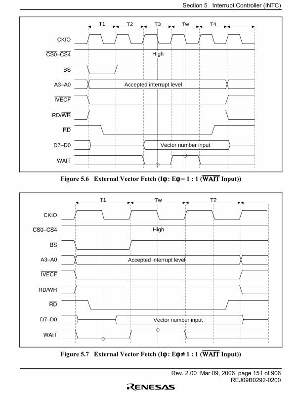
Section 5 Interrupt Controller (INTC)
Rev. 2.00 Mar 09, 2006 page 151 of 906REJ09B0292-0200
CKIO
CS0–CS4
BS
A3–A0
IVECF
RD/WR
RD
D7–D0
WAIT
T1 T2 T3 Tw T4
Vector number input
Accepted interrupt level
High
Figure 5.6 External Vector Fetch (Iφφφφ : Eφφφφ = 1 : 1 (WAITWAITWAITWAIT Input))
CKIO
CS0–CS4
BS
A3–A0
IVECF
RD/WR
RD
D7–D0
WAIT
T1 Tw T2
Accepted interrupt level
High
Vector number input
Figure 5.7 External Vector Fetch (Iφφφφ : Eφφφφ ≠≠≠≠ 1 : 1 (WAITWAITWAITWAIT Input))
Section 5 Interrupt Controller (INTC)
Rev. 2.00 Mar 09, 2006 page 152 of 906REJ09B0292-0200
5.2.6 On-chip Peripheral Module Interrupts
On-chip peripheral module interrupts are interrupts generated by the following 9 on-chipperipheral modules:
• Direct memory access controller (DMAC)• Bus state controller (BSC)• Watchdog timer (WDT)• 16-bit free-running timer (FRT)• Ethernet controller direct memory access controller (E-DMAC) (Including EtherC interrupt)• 16-bit timer pulse unit (TPU)• Serial communication interface with FIFO (SCIF)• Serial I/O with FIFO (SIOF)• Serial I/O (SIO)
A different interrupt vector is assigned to each interrupt source, so the exception service routinedoes not have to decide which interrupt has occurred. Priority levels between 0 and 15 can beassigned to individual on-chip peripheral modules in interrupt priority registers A, B, D, and E(IPRA, IPRB, IPRD, IPRE). On-chip peripheral module interrupt exception handling sets theinterrupt mask level bits (I3�I0) in the status register (SR) to the priority level value of the on-chipperipheral module interrupt that was accepted.
5.2.7 Interrupt Exception Vectors and Priority Order
Table 5.4 lists interrupt sources and their vector numbers, vector table address offsets and interruptpriorities.
Each interrupt source is allocated a different vector number and vector table address offset. Vectortable addresses are calculated from vector numbers and vector table address offsets. In interruptexception handling, the exception service routine start address is fetched from the vector tableentry indicated by the vector table address. See table 4.4, Calculating Exception Vector TableAddresses, in section 4, Exception Handling, for more information on this calculation.
IRL interrupts IRL15�IRL1 have interrupt priority levels of 15�1, respectively. IRQ interrupt andon-chip peripheral module interrupt priorities can be set freely between 0 and 15 for each moduleby setting interrupt priority registers A�E (IPRA�IPRE). The ranking of interrupt sources forIPRA�IPRE, however, must be the order listed under Priority within IPR Setting Unit in table 5.4and cannot be changed. A reset assigns priority level 0 to on-chip peripheral module interrupts. Ifthe same priority level is assigned to two or more interrupt sources and interrupts from those
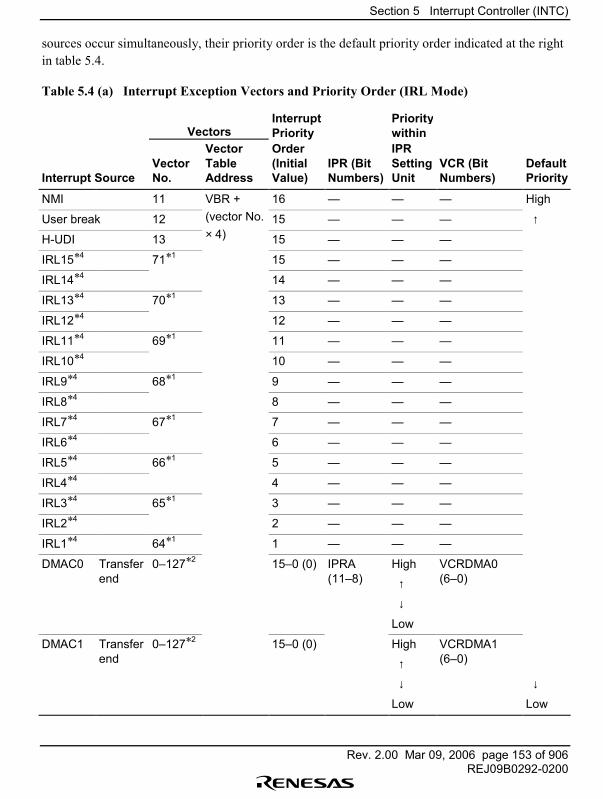
Section 5 Interrupt Controller (INTC)
Rev. 2.00 Mar 09, 2006 page 153 of 906REJ09B0292-0200
sources occur simultaneously, their priority order is the default priority order indicated at the rightin table 5.4.
Table 5.4 (a) Interrupt Exception Vectors and Priority Order (IRL Mode)
VectorsInterruptPriority
Prioritywithin
Interrupt SourceVectorNo.
VectorTableAddress
Order(InitialValue)
IPR (BitNumbers)
IPRSettingUnit
VCR (BitNumbers)
DefaultPriority
NMI 11 VBR + 16 � � � High
User break 12 (vector No. 15 � � � ↑
H-UDI 13 × 4) 15 � � �
IRL15*4 71*1 15 � � �
IRL14*4 14 � � �
IRL13*4 70*1 13 � � �
IRL12*4 12 � � �
IRL11*4 69*1 11 � � �
IRL10*4 10 � � �
IRL9*4 68*1 9 � � �
IRL8*4 8 � � �
IRL7*4 67*1 7 � � �
IRL6*4 6 � � �
IRL5*4 66*1 5 � � �
IRL4*4 4 � � �
IRL3*4 65*1 3 � � �
IRL2*4 2 � � �
IRL1*4 64*1 1 � � �
DMAC0 Transferend
0�127*2 15�0 (0) IPRA(11�8)
High
↑
↓
Low
VCRDMA0(6�0)
DMAC1 Transferend
0�127*2 15�0 (0) High
↑
↓
Low
VCRDMA1(6�0)
↓
Low
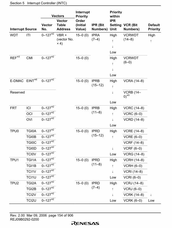
Section 5 Interrupt Controller (INTC)
Rev. 2.00 Mar 09, 2006 page 154 of 906REJ09B0292-0200
VectorsInterruptPriority
Prioritywithin
Interrupt SourceVectorNo.
VectorTableAddress
Order(InitialValue)
IPR (BitNumbers)
IPRSettingUnit
VCR (BitNumbers)
DefaultPriority
WDT ITI 0�127*2 VBR +(vector No.× 4)
15�0 (0) IPRA(7�4)
High
↑
↓
Low
VCRWDT(14�8)
High
↑
REF*3 CMI 0�127*2 15�0 (0) High
↑
↓
Low
VCRWDT(6�0)
E-DMAC EINT*6 0�127*2 15�0 (0) IPRB High VCRA (14�8)(15�12) ↑
Reserved ↓ VCRB (14�0)*5
Low
FRT ICI 0�127*2 15�0 (0) IPRB High VCRC (14�8)
OCI 0�127*2 (11�8) ↑ VCRC (6�0)
OVI 0�127*2 ↓
Low
VCRD (14�8)
TPU0 TGI0A 0�127*2 15�0 (0) IPRD High VCRE (14�8)
TGI0B 0�127*2 (15�12) ↑ VCRE (6�0)
TGI0C 0�127*2 VCRF (14�8)
TGI0D 0�127*2 ↓ VCRF (6�0)
TCI0V 0�127*2 Low VCRG (14�8)
TPU1 TGI1A 0�127*2 15�0 (0) IPRD High VCRH (14�8)
TGI1B 0�127*2 (11�8) ↑ VCRH (6�0)
TCI1V 0�127*2 ↓ VCRI (14�8)
TCI1U 0�127*2 Low VCRI (6�0)
TPU2 TGI2A 0�127*2 15�0 (0) IPRD High VCRJ (14�8)
TGI2B 0�127*2 (7�4) ↑ VCRJ (6�0)
TCI2V 0�127*2 ↓ VCRK (14�8) ↓
TCI2U 0�127*2 Low VCRK (6�0) Low
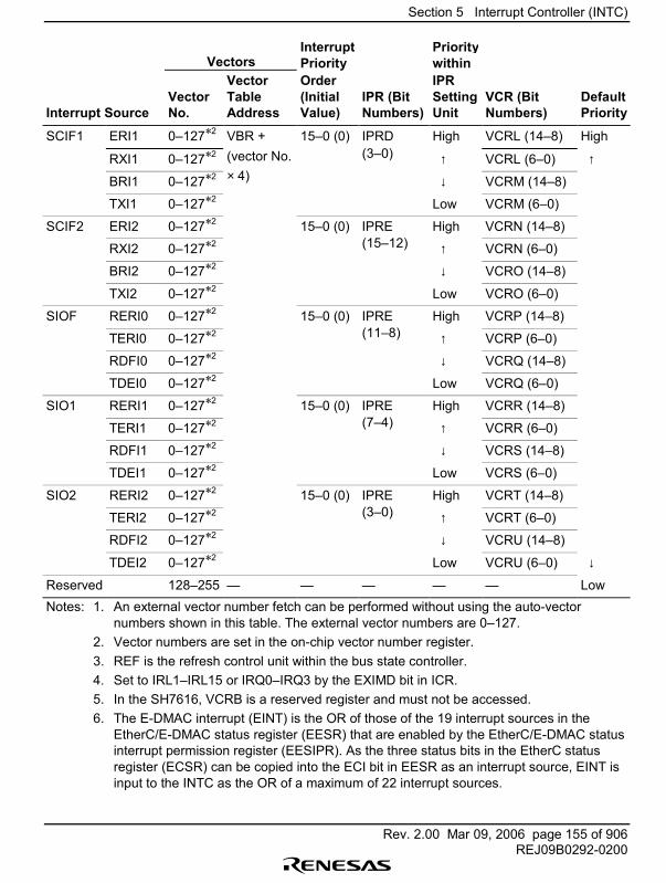
Section 5 Interrupt Controller (INTC)
Rev. 2.00 Mar 09, 2006 page 155 of 906REJ09B0292-0200
VectorsInterruptPriority
Prioritywithin
Interrupt SourceVectorNo.
VectorTableAddress
Order(InitialValue)
IPR (BitNumbers)
IPRSettingUnit
VCR (BitNumbers)
DefaultPriority
SCIF1 ERI1 0�127*2 VBR + 15�0 (0) IPRD High VCRL (14�8) High
RXI1 0�127*2 (vector No. (3�0) ↑ VCRL (6�0) ↑
BRI1 0�127*2 × 4) ↓ VCRM (14�8)
TXI1 0�127*2 Low VCRM (6�0)
SCIF2 ERI2 0�127*2 15�0 (0) IPRE High VCRN (14�8)
RXI2 0�127*2 (15�12) ↑ VCRN (6�0)
BRI2 0�127*2 ↓ VCRO (14�8)
TXI2 0�127*2 Low VCRO (6�0)
SIOF RERI0 0�127*2 15�0 (0) IPRE High VCRP (14�8)
TERI0 0�127*2 (11�8) ↑ VCRP (6�0)
RDFI0 0�127*2 ↓ VCRQ (14�8)
TDEI0 0�127*2 Low VCRQ (6�0)
SIO1 RERI1 0�127*2 15�0 (0) IPRE High VCRR (14�8)
TERI1 0�127*2 (7�4) ↑ VCRR (6�0)
RDFI1 0�127*2 ↓ VCRS (14�8)
TDEI1 0�127*2 Low VCRS (6�0)
SIO2 RERI2 0�127*2 15�0 (0) IPRE High VCRT (14�8)
TERI2 0�127*2 (3�0) ↑ VCRT (6�0)
RDFI2 0�127*2 ↓ VCRU (14�8)
TDEI2 0�127*2 Low VCRU (6�0) ↓
Reserved 128�255 � � � � � LowNotes: 1. An external vector number fetch can be performed without using the auto-vector
numbers shown in this table. The external vector numbers are 0�127.2. Vector numbers are set in the on-chip vector number register.3. REF is the refresh control unit within the bus state controller.4. Set to IRL1�IRL15 or IRQ0�IRQ3 by the EXIMD bit in ICR.5. In the SH7616, VCRB is a reserved register and must not be accessed.6. The E-DMAC interrupt (EINT) is the OR of those of the 19 interrupt sources in the
EtherC/E-DMAC status register (EESR) that are enabled by the EtherC/E-DMAC statusinterrupt permission register (EESIPR). As the three status bits in the EtherC statusregister (ECSR) can be copied into the ECI bit in EESR as an interrupt source, EINT isinput to the INTC as the OR of a maximum of 22 interrupt sources.
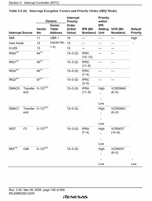
Section 5 Interrupt Controller (INTC)
Rev. 2.00 Mar 09, 2006 page 156 of 906REJ09B0292-0200
Table 5.4 (b) Interrupt Exception Vectors and Priority Order (IRQ Mode)
VectorsInterruptPriority
Prioritywithin
Interrupt SourceVectorNo.
VectorTableAddress
Order(InitialValue)
IPR (BitNumbers)
IPRSettingUnit
VCR (BitNumbers)
DefaultPriority
NMI 11 VBR + 16 � � � High
User break 12 (vector No. 15 � � � ↑
H-UDI 13 × 4) 15 � � �
IRQ0*4 64*1 15�0 (0) IPRC(15�12)
� �
IRQ1*4 65*1 15�0 (0) IPRC(11�8)
� �
IRQ2*4 66*1 15�0 (0) IPRC(7�4)
� �
IRQ3*4 67*1 15�0 (0) IPRC(3�0)
� �
DMAC0 Transferend
0�127*2 15�0 (0) IPRA(11�8)
High
↑
↓
Low
VCRDMA0(6�0)
DMAC1 Transferend
0�127*2 15�0 (0) High
↑
↓
Low
VCRDMA1(6�0)
WDT ITI 0�127*2 15�0 (0) IPRA(7�4)
High
↑
↓
Low
VCRWDT(14�8)
REF*3 CMI 0�127*2 15�0 (0) High
↑
↓
Low
VCRWDT(6�0)
↓
Low
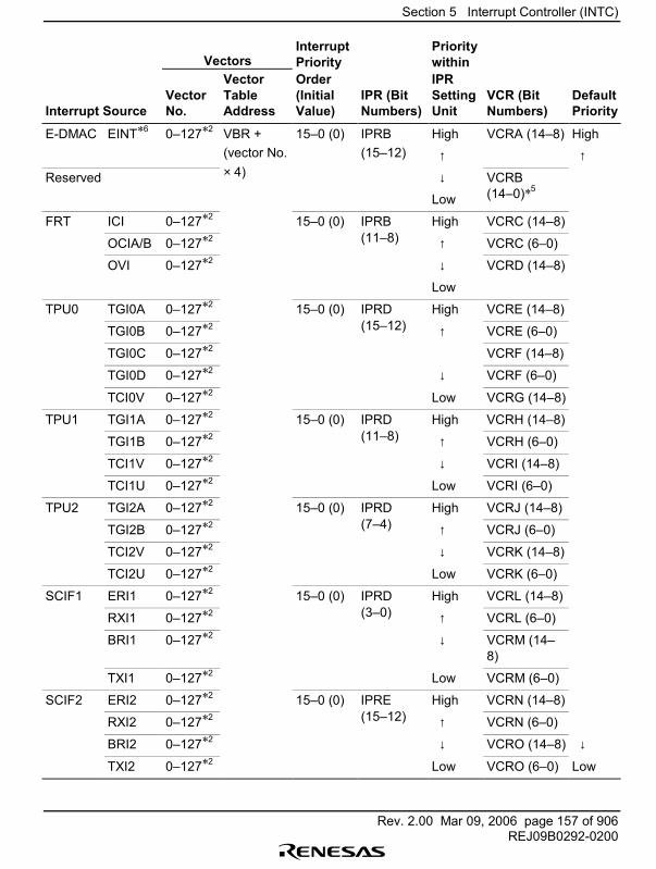
Section 5 Interrupt Controller (INTC)
Rev. 2.00 Mar 09, 2006 page 157 of 906REJ09B0292-0200
VectorsInterruptPriority
Prioritywithin
Interrupt SourceVectorNo.
VectorTableAddress
Order(InitialValue)
IPR (BitNumbers)
IPRSettingUnit
VCR (BitNumbers)
DefaultPriority
E-DMAC EINT*6 0�127*2 VBR + 15�0 (0) IPRB High VCRA (14�8) High(vector No. (15�12) ↑ ↑
Reserved × 4) ↓ VCRB
Low (14�0)*5
FRT ICI 0�127*2 15�0 (0) IPRB High VCRC (14�8)
OCIA/B 0�127*2 (11�8) ↑ VCRC (6�0)
OVI 0�127*2 ↓
Low
VCRD (14�8)
TPU0 TGI0A 0�127*2 15�0 (0) IPRD High VCRE (14�8)
TGI0B 0�127*2 (15�12) ↑ VCRE (6�0)
TGI0C 0�127*2 VCRF (14�8)
TGI0D 0�127*2 ↓ VCRF (6�0)
TCI0V 0�127*2 Low VCRG (14�8)
TPU1 TGI1A 0�127*2 15�0 (0) IPRD High VCRH (14�8)
TGI1B 0�127*2 (11�8) ↑ VCRH (6�0)
TCI1V 0�127*2 ↓ VCRI (14�8)
TCI1U 0�127*2 Low VCRI (6�0)
TPU2 TGI2A 0�127*2 15�0 (0) IPRD High VCRJ (14�8)
TGI2B 0�127*2 (7�4) ↑ VCRJ (6�0)
TCI2V 0�127*2 ↓ VCRK (14�8)
TCI2U 0�127*2 Low VCRK (6�0)
SCIF1 ERI1 0�127*2 15�0 (0) IPRD High VCRL (14�8)
RXI1 0�127*2 (3�0) ↑ VCRL (6�0)
BRI1 0�127*2 ↓ VCRM (14�8)
TXI1 0�127*2 Low VCRM (6�0)
SCIF2 ERI2 0�127*2 15�0 (0) IPRE High VCRN (14�8)
RXI2 0�127*2 (15�12) ↑ VCRN (6�0)
BRI2 0�127*2 ↓ VCRO (14�8) ↓
TXI2 0�127*2 Low VCRO (6�0) Low
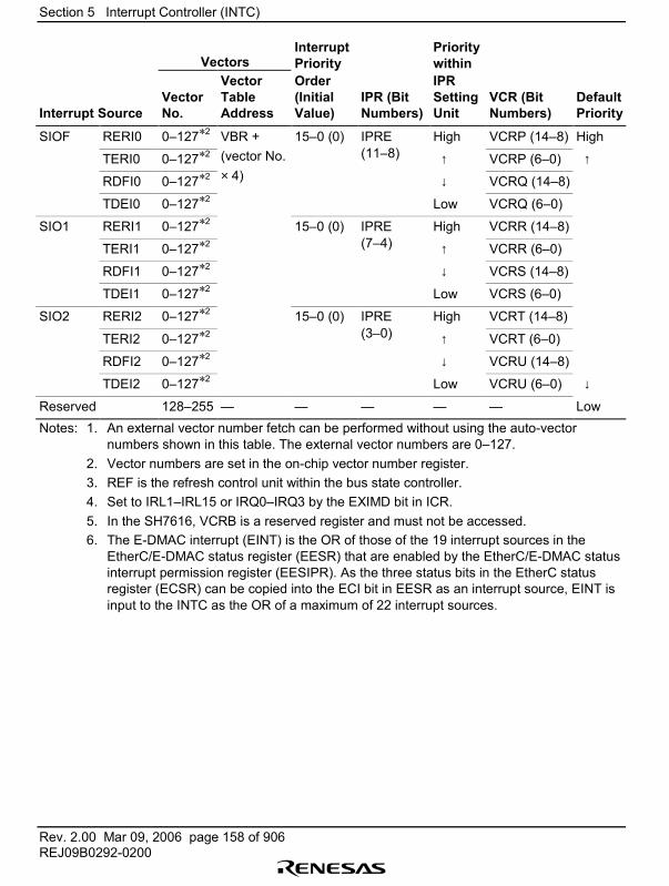
Section 5 Interrupt Controller (INTC)
Rev. 2.00 Mar 09, 2006 page 158 of 906REJ09B0292-0200
VectorsInterruptPriority
Prioritywithin
Interrupt SourceVectorNo.
VectorTableAddress
Order(InitialValue)
IPR (BitNumbers)
IPRSettingUnit
VCR (BitNumbers)
DefaultPriority
SIOF RERI0 0�127*2 VBR + 15�0 (0) IPRE High VCRP (14�8) High
TERI0 0�127*2 (vector No. (11�8) ↑ VCRP (6�0) ↑
RDFI0 0�127*2 × 4) ↓ VCRQ (14�8)
TDEI0 0�127*2 Low VCRQ (6�0)
SIO1 RERI1 0�127*2 15�0 (0) IPRE High VCRR (14�8)
TERI1 0�127*2 (7�4) ↑ VCRR (6�0)
RDFI1 0�127*2 ↓ VCRS (14�8)
TDEI1 0�127*2 Low VCRS (6�0)
SIO2 RERI2 0�127*2 15�0 (0) IPRE High VCRT (14�8)
TERI2 0�127*2 (3�0) ↑ VCRT (6�0)
RDFI2 0�127*2 ↓ VCRU (14�8)
TDEI2 0�127*2 Low VCRU (6�0) ↓
Reserved 128�255 � � � � � LowNotes: 1. An external vector number fetch can be performed without using the auto-vector
numbers shown in this table. The external vector numbers are 0�127.2. Vector numbers are set in the on-chip vector number register.3. REF is the refresh control unit within the bus state controller.4. Set to IRL1�IRL15 or IRQ0�IRQ3 by the EXIMD bit in ICR.5. In the SH7616, VCRB is a reserved register and must not be accessed.6. The E-DMAC interrupt (EINT) is the OR of those of the 19 interrupt sources in the
EtherC/E-DMAC status register (EESR) that are enabled by the EtherC/E-DMAC statusinterrupt permission register (EESIPR). As the three status bits in the EtherC statusregister (ECSR) can be copied into the ECI bit in EESR as an interrupt source, EINT isinput to the INTC as the OR of a maximum of 22 interrupt sources.
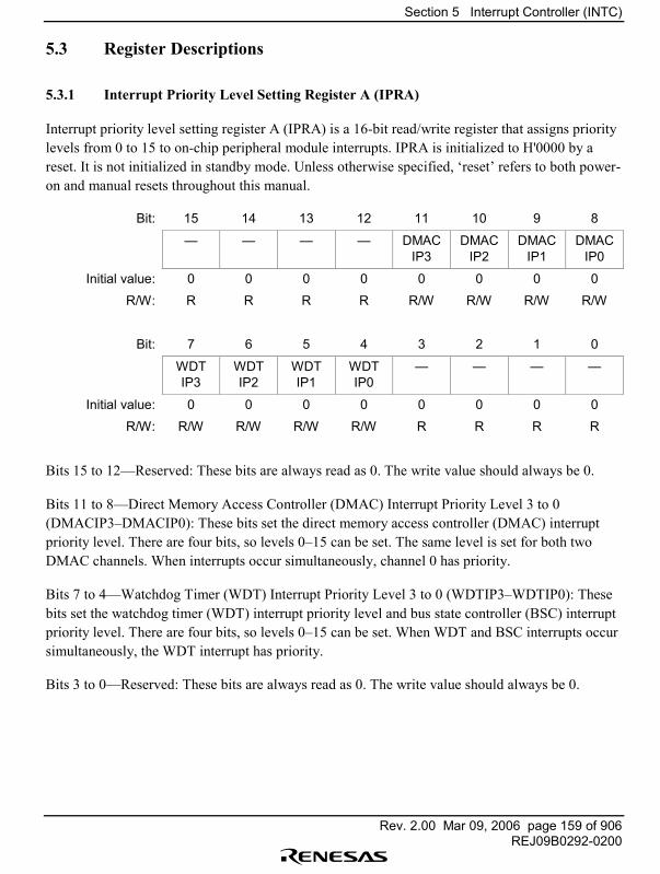
Section 5 Interrupt Controller (INTC)
Rev. 2.00 Mar 09, 2006 page 159 of 906REJ09B0292-0200
5.3 Register Descriptions
5.3.1 Interrupt Priority Level Setting Register A (IPRA)
Interrupt priority level setting register A (IPRA) is a 16-bit read/write register that assigns prioritylevels from 0 to 15 to on-chip peripheral module interrupts. IPRA is initialized to H'0000 by areset. It is not initialized in standby mode. Unless otherwise specified, �reset� refers to both power-on and manual resets throughout this manual.
Bit: 15 14 13 12 11 10 9 8
� � � � DMACIP3
DMACIP2
DMACIP1
DMACIP0
Initial value: 0 0 0 0 0 0 0 0
R/W: R R R R R/W R/W R/W R/W
Bit: 7 6 5 4 3 2 1 0
WDTIP3
WDTIP2
WDTIP1
WDTIP0
� � � �
Initial value: 0 0 0 0 0 0 0 0
R/W: R/W R/W R/W R/W R R R R
Bits 15 to 12�Reserved: These bits are always read as 0. The write value should always be 0.
Bits 11 to 8�Direct Memory Access Controller (DMAC) Interrupt Priority Level 3 to 0(DMACIP3�DMACIP0): These bits set the direct memory access controller (DMAC) interruptpriority level. There are four bits, so levels 0�15 can be set. The same level is set for both twoDMAC channels. When interrupts occur simultaneously, channel 0 has priority.
Bits 7 to 4�Watchdog Timer (WDT) Interrupt Priority Level 3 to 0 (WDTIP3�WDTIP0): Thesebits set the watchdog timer (WDT) interrupt priority level and bus state controller (BSC) interruptpriority level. There are four bits, so levels 0�15 can be set. When WDT and BSC interrupts occursimultaneously, the WDT interrupt has priority.
Bits 3 to 0�Reserved: These bits are always read as 0. The write value should always be 0.
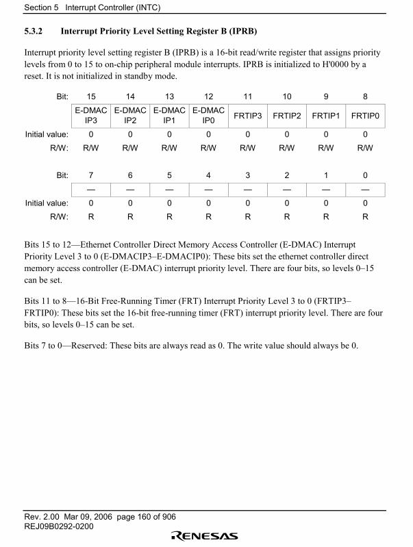
Section 5 Interrupt Controller (INTC)
Rev. 2.00 Mar 09, 2006 page 160 of 906REJ09B0292-0200
5.3.2 Interrupt Priority Level Setting Register B (IPRB)
Interrupt priority level setting register B (IPRB) is a 16-bit read/write register that assigns prioritylevels from 0 to 15 to on-chip peripheral module interrupts. IPRB is initialized to H'0000 by areset. It is not initialized in standby mode.
Bit: 15 14 13 12 11 10 9 8
E-DMACIP3
E-DMACIP2
E-DMACIP1
E-DMACIP0 FRTIP3 FRTIP2 FRTIP1 FRTIP0
Initial value: 0 0 0 0 0 0 0 0
R/W: R/W R/W R/W R/W R/W R/W R/W R/W
Bit: 7 6 5 4 3 2 1 0
� � � � � � � �
Initial value: 0 0 0 0 0 0 0 0
R/W: R R R R R R R R
Bits 15 to 12�Ethernet Controller Direct Memory Access Controller (E-DMAC) InterruptPriority Level 3 to 0 (E-DMACIP3�E-DMACIP0): These bits set the ethernet controller directmemory access controller (E-DMAC) interrupt priority level. There are four bits, so levels 0�15can be set.
Bits 11 to 8�16-Bit Free-Running Timer (FRT) Interrupt Priority Level 3 to 0 (FRTIP3�FRTIP0): These bits set the 16-bit free-running timer (FRT) interrupt priority level. There are fourbits, so levels 0�15 can be set.
Bits 7 to 0�Reserved: These bits are always read as 0. The write value should always be 0.
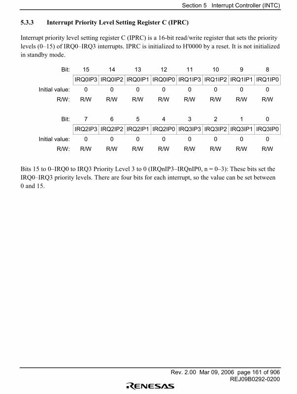
Section 5 Interrupt Controller (INTC)
Rev. 2.00 Mar 09, 2006 page 161 of 906REJ09B0292-0200
5.3.3 Interrupt Priority Level Setting Register C (IPRC)
Interrupt priority level setting register C (IPRC) is a 16-bit read/write register that sets the prioritylevels (0�15) of IRQ0�IRQ3 interrupts. IPRC is initialized to H'0000 by a reset. It is not initializedin standby mode.
Bit: 15 14 13 12 11 10 9 8
IRQ0IP3 IRQ0IP2 IRQ0IP1 IRQ0IP0 IRQ1IP3 IRQ1IP2 IRQ1IP1 IRQ1IP0
Initial value: 0 0 0 0 0 0 0 0
R/W: R/W R/W R/W R/W R/W R/W R/W R/W
Bit: 7 6 5 4 3 2 1 0
IRQ2IP3 IRQ2IP2 IRQ2IP1 IRQ2IP0 IRQ3IP3 IRQ3IP2 IRQ3IP1 IRQ3IP0
Initial value: 0 0 0 0 0 0 0 0
R/W: R/W R/W R/W R/W R/W R/W R/W R/W
Bits 15 to 0�IRQ0 to IRQ3 Priority Level 3 to 0 (IRQnIP3�IRQnIP0, n = 0�3): These bits set theIRQ0�IRQ3 priority levels. There are four bits for each interrupt, so the value can be set between0 and 15.
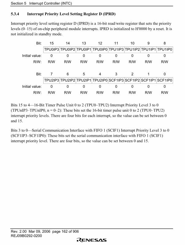
Section 5 Interrupt Controller (INTC)
Rev. 2.00 Mar 09, 2006 page 162 of 906REJ09B0292-0200
5.3.4 Interrupt Priority Level Setting Register D (IPRD)
Interrupt priority level setting register D (IPRD) is a 16-bit read/write register that sets the prioritylevels (0�15) of on-chip peripheral module interrupts. IPRD is initialized to H'0000 by a reset. It isnot initialized in standby mode.
Bit: 15 14 13 12 11 10 9 8
TPU0IP3 TPU0IP2 TPU0IP1 TPU0IP0 TPU1IP3 TPU1IP2 TPU1IP1 TPU1IP0
Initial value: 0 0 0 0 0 0 0 0
R/W: R/W R/W R/W R/W R/W R/W R/W R/W
Bit: 7 6 5 4 3 2 1 0
TPU2IP3 TPU2IP2 TPU2IP1 TPU2IP0 SCF1IP3 SCF1IP2 SCF1IP1 SCF1IP0
Initial value: 0 0 0 0 0 0 0 0
R/W: R/W R/W R/W R/W R/W R/W R/W R/W
Bits 15 to 4�16-Bit Timer Pulse Unit 0 to 2 (TPU0�TPU2) Interrupt Priority Level 3 to 0(TPUnIP3�TPUnIP0, n = 0�2): These bits set the 16-bit timer pulse unit 0 to 2 (TPU0�TPU2)interrupt priority levels. There are four bits for each interrupt, so the value can be set between 0and 15.
Bits 3 to 0�Serial Communication Interface with FIFO 1 (SCIF1) Interrupt Priority Level 3 to 0(SCF1IP3�SCF1IP0): These bits set the serial communication interface with FIFO 1 (SCIF1)interrupt priority level. There are four bits, so the value can be set between 0 and 15.
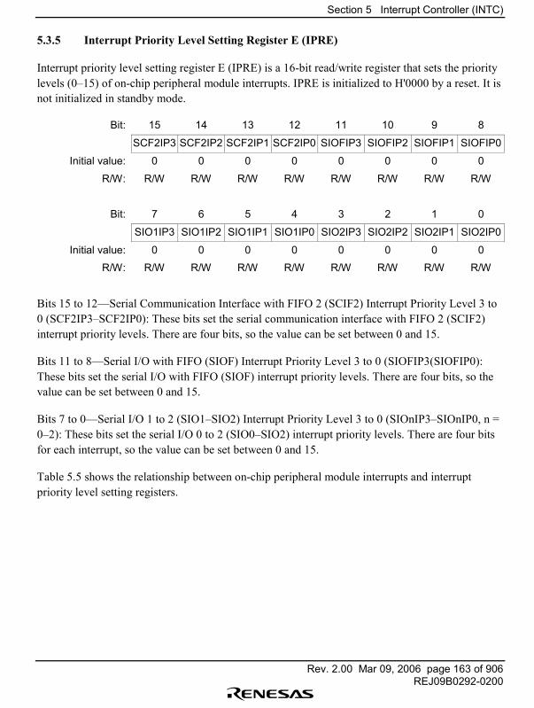
Section 5 Interrupt Controller (INTC)
Rev. 2.00 Mar 09, 2006 page 163 of 906REJ09B0292-0200
5.3.5 Interrupt Priority Level Setting Register E (IPRE)
Interrupt priority level setting register E (IPRE) is a 16-bit read/write register that sets the prioritylevels (0�15) of on-chip peripheral module interrupts. IPRE is initialized to H'0000 by a reset. It isnot initialized in standby mode.
Bit: 15 14 13 12 11 10 9 8
SCF2IP3 SCF2IP2 SCF2IP1 SCF2IP0 SIOFIP3 SIOFIP2 SIOFIP1 SIOFIP0
Initial value: 0 0 0 0 0 0 0 0
R/W: R/W R/W R/W R/W R/W R/W R/W R/W
Bit: 7 6 5 4 3 2 1 0
SIO1IP3 SIO1IP2 SIO1IP1 SIO1IP0 SIO2IP3 SIO2IP2 SIO2IP1 SIO2IP0
Initial value: 0 0 0 0 0 0 0 0
R/W: R/W R/W R/W R/W R/W R/W R/W R/W
Bits 15 to 12�Serial Communication Interface with FIFO 2 (SCIF2) Interrupt Priority Level 3 to0 (SCF2IP3�SCF2IP0): These bits set the serial communication interface with FIFO 2 (SCIF2)interrupt priority levels. There are four bits, so the value can be set between 0 and 15.
Bits 11 to 8��Serial I/O with FIFO (SIOF) Interrupt Priority Level 3 to 0 (SIOFIP3(SIOFIP0):These bits set the serial I/O with FIFO (SIOF) interrupt priority levels. There are four bits, so thevalue can be set between 0 and 15.
Bits 7 to 0�Serial I/O 1 to 2 (SIO1�SIO2) Interrupt Priority Level 3 to 0 (SIOnIP3�SIOnIP0, n =0�2): These bits set the serial I/O 0 to 2 (SIO0�SIO2) interrupt priority levels. There are four bitsfor each interrupt, so the value can be set between 0 and 15.
Table 5.5 shows the relationship between on-chip peripheral module interrupts and interruptpriority level setting registers.
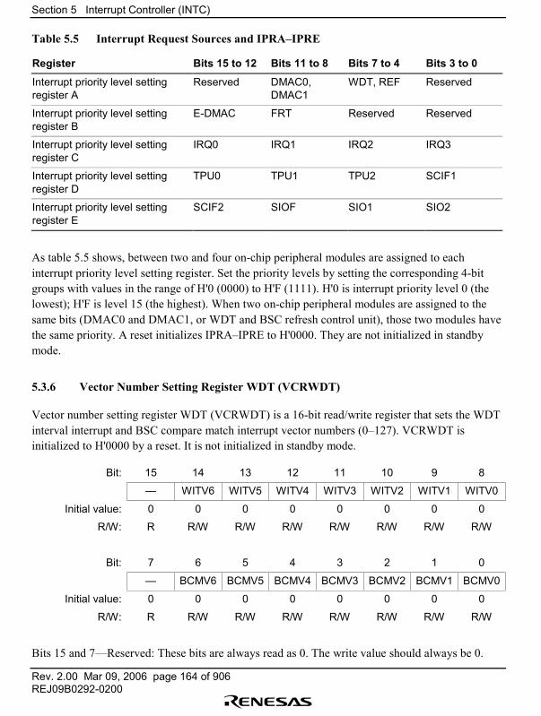
Section 5 Interrupt Controller (INTC)
Rev. 2.00 Mar 09, 2006 page 164 of 906REJ09B0292-0200
Table 5.5 Interrupt Request Sources and IPRA�IPRE
Register Bits 15 to 12 Bits 11 to 8 Bits 7 to 4 Bits 3 to 0
Interrupt priority level settingregister A
Reserved DMAC0,DMAC1
WDT, REF Reserved
Interrupt priority level settingregister B
E-DMAC FRT Reserved Reserved
Interrupt priority level settingregister C
IRQ0 IRQ1 IRQ2 IRQ3
Interrupt priority level settingregister D
TPU0 TPU1 TPU2 SCIF1
Interrupt priority level settingregister E
SCIF2 SIOF SIO1 SIO2
As table 5.5 shows, between two and four on-chip peripheral modules are assigned to eachinterrupt priority level setting register. Set the priority levels by setting the corresponding 4-bitgroups with values in the range of H'0 (0000) to H'F (1111). H'0 is interrupt priority level 0 (thelowest); H'F is level 15 (the highest). When two on-chip peripheral modules are assigned to thesame bits (DMAC0 and DMAC1, or WDT and BSC refresh control unit), those two modules havethe same priority. A reset initializes IPRA�IPRE to H'0000. They are not initialized in standbymode.
5.3.6 Vector Number Setting Register WDT (VCRWDT)
Vector number setting register WDT (VCRWDT) is a 16-bit read/write register that sets the WDTinterval interrupt and BSC compare match interrupt vector numbers (0�127). VCRWDT isinitialized to H'0000 by a reset. It is not initialized in standby mode.
Bit: 15 14 13 12 11 10 9 8
� WITV6 WITV5 WITV4 WITV3 WITV2 WITV1 WITV0
Initial value: 0 0 0 0 0 0 0 0
R/W: R R/W R/W R/W R/W R/W R/W R/W
Bit: 7 6 5 4 3 2 1 0
� BCMV6 BCMV5 BCMV4 BCMV3 BCMV2 BCMV1 BCMV0
Initial value: 0 0 0 0 0 0 0 0
R/W: R R/W R/W R/W R/W R/W R/W R/W
Bits 15 and 7�Reserved: These bits are always read as 0. The write value should always be 0.
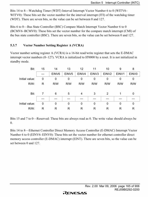
Section 5 Interrupt Controller (INTC)
Rev. 2.00 Mar 09, 2006 page 165 of 906REJ09B0292-0200
Bits 14 to 8�Watchdog Timer (WDT) Interval Interrupt Vector Number 6 to 0 (WITV6�WITV0): These bits set the vector number for the interval interrupt (ITI) of the watchdog timer(WDT). There are seven bits, so the value can be set between 0 and 127.
Bits 6 to 0�Bus State Controller (BSC) Compare Match Interrupt Vector Number 6 to 0(BCMV6�BCMV0): These bits set the vector number for the compare match interrupt (CMI) ofthe bus state controller (BSC). There are seven bits, so the value can be set between 0 and 127.
5.3.7 Vector Number Setting Register A (VCRA)
Vector number setting register A (VCRA) is a 16-bit read/write register that sets the E-DMACinterrupt vector numbers (0�127). VCRA is initialized to H'0000 by a reset. It is not initialized instandby mode.
Bit: 15 14 13 12 11 10 9 8
� EINV6 EINV5 EINV4 EINV3 EINV2 EINV1 EINV0
Initial value: 0 0 0 0 0 0 0 0
R/W: R R/W R/W R/W R/W R/W R/W R/W
Bit: 7 6 5 4 3 2 1 0
� � � � � � � �
Initial value: 0 0 0 0 0 0 0 0
R/W: R R R R R R R R
Bits 15 and 7 to 0�Reserved: These bits are always read as 0. The write value should always be0.
Bits 14 to 8�Ethernet Controller Direct Memory Access Controller (E-DMAC) Interrupt VectorNumber 6 to 0 (EINV6�EINV0): These bits set the vector number for ethernet controller directmemory access controller (E-DMAC) interrupt (EINT). There are seven bits, so the value can beset between 0 and 127.
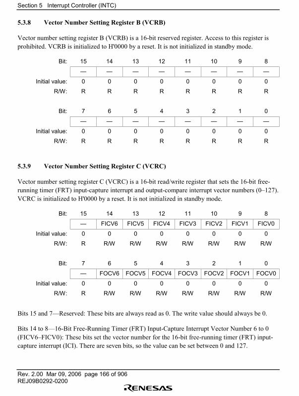
Section 5 Interrupt Controller (INTC)
Rev. 2.00 Mar 09, 2006 page 166 of 906REJ09B0292-0200
5.3.8 Vector Number Setting Register B (VCRB)
Vector number setting register B (VCRB) is a 16-bit reserved register. Access to this register isprohibited. VCRB is initialized to H'0000 by a reset. It is not initialized in standby mode.
Bit: 15 14 13 12 11 10 9 8
� � � � � � � �
Initial value: 0 0 0 0 0 0 0 0
R/W: R R R R R R R R
Bit: 7 6 5 4 3 2 1 0
� � � � � � � �
Initial value: 0 0 0 0 0 0 0 0
R/W: R R R R R R R R
5.3.9 Vector Number Setting Register C (VCRC)
Vector number setting register C (VCRC) is a 16-bit read/write register that sets the 16-bit free-running timer (FRT) input-capture interrupt and output-compare interrupt vector numbers (0�127).VCRC is initialized to H'0000 by a reset. It is not initialized in standby mode.
Bit: 15 14 13 12 11 10 9 8
� FICV6 FICV5 FICV4 FICV3 FICV2 FICV1 FICV0
Initial value: 0 0 0 0 0 0 0 0
R/W: R R/W R/W R/W R/W R/W R/W R/W
Bit: 7 6 5 4 3 2 1 0
� FOCV6 FOCV5 FOCV4 FOCV3 FOCV2 FOCV1 FOCV0
Initial value: 0 0 0 0 0 0 0 0
R/W: R R/W R/W R/W R/W R/W R/W R/W
Bits 15 and 7�Reserved: These bits are always read as 0. The write value should always be 0.
Bits 14 to 8�16-Bit Free-Running Timer (FRT) Input-Capture Interrupt Vector Number 6 to 0(FICV6�FICV0): These bits set the vector number for the 16-bit free-running timer (FRT) input-capture interrupt (ICI). There are seven bits, so the value can be set between 0 and 127.
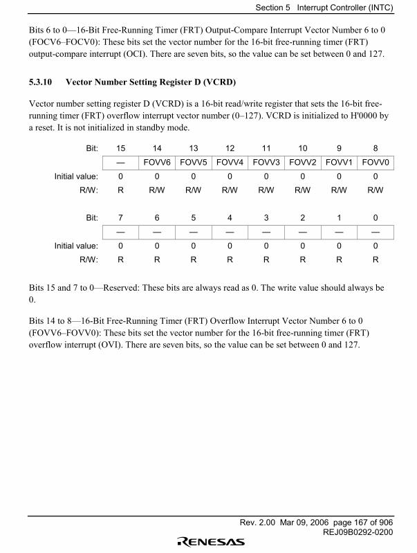
Section 5 Interrupt Controller (INTC)
Rev. 2.00 Mar 09, 2006 page 167 of 906REJ09B0292-0200
Bits 6 to 0�16-Bit Free-Running Timer (FRT) Output-Compare Interrupt Vector Number 6 to 0(FOCV6�FOCV0): These bits set the vector number for the 16-bit free-running timer (FRT)output-compare interrupt (OCI). There are seven bits, so the value can be set between 0 and 127.
5.3.10 Vector Number Setting Register D (VCRD)
Vector number setting register D (VCRD) is a 16-bit read/write register that sets the 16-bit free-running timer (FRT) overflow interrupt vector number (0�127). VCRD is initialized to H'0000 bya reset. It is not initialized in standby mode.
Bit: 15 14 13 12 11 10 9 8
� FOVV6 FOVV5 FOVV4 FOVV3 FOVV2 FOVV1 FOVV0
Initial value: 0 0 0 0 0 0 0 0
R/W: R R/W R/W R/W R/W R/W R/W R/W
Bit: 7 6 5 4 3 2 1 0
� � � � � � � �
Initial value: 0 0 0 0 0 0 0 0
R/W: R R R R R R R R
Bits 15 and 7 to 0�Reserved: These bits are always read as 0. The write value should always be0.
Bits 14 to 8�16-Bit Free-Running Timer (FRT) Overflow Interrupt Vector Number 6 to 0(FOVV6�FOVV0): These bits set the vector number for the 16-bit free-running timer (FRT)overflow interrupt (OVI). There are seven bits, so the value can be set between 0 and 127.
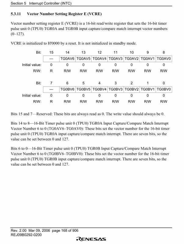
Section 5 Interrupt Controller (INTC)
Rev. 2.00 Mar 09, 2006 page 168 of 906REJ09B0292-0200
5.3.11 Vector Number Setting Register E (VCRE)
Vector number setting register E (VCRE) is a 16-bit read/write register that sets the 16-bit timerpulse unit 0 (TPU0) TGR0A and TGR0B input capture/compare match interrupt vector numbers(0�127).
VCRE is initialized to H'0000 by a reset. It is not initialized in standby mode.
Bit: 15 14 13 12 11 10 9 8
� TG0AV6 TG0AV5 TG0AV4 TG0AV3 TG0AV2 TG0AV1 TG0AV0
Initial value: 0 0 0 0 0 0 0 0
R/W: R R/W R/W R/W R/W R/W R/W R/W
Bit: 7 6 5 4 3 2 1 0
� TG0BV6 TG0BV5 TG0BV4 TG0BV3 TG0BV2 TG0BV1 TG0BV0
Initial value: 0 0 0 0 0 0 0 0
R/W: R R/W R/W R/W R/W R/W R/W R/W
Bits 15 and 7�Reserved: These bits are always read as 0. The write value should always be 0.
Bits 14 to 8�16-Bit Timer pulse unit 0 (TPU0) TGR0A Input Capture/Compare Match InterruptVector Number 6 to 0 (TG0AV6�TG0AV0): These bits set the vector number for the 16-bit timerpulse unit 0 (TPU0) TGR0A input capture/compare match interrupt. There are seven bits, so thevalue can be set between 0 and 127.
Bits 6 to 0�16-Bit Timer pulse unit 0 (TPU0) TGR0B Input Capture/Compare Match InterruptVector Number 6 to 0 (TG0BV6�TG0BV0): These bits set the vector number for the 16-bit timerpulse unit 0 (TPU0) TGR0B input capture/compare match interrupt. There are seven bits, so thevalue can be set between 0 and 127.
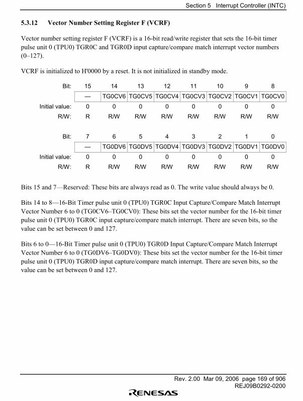
Section 5 Interrupt Controller (INTC)
Rev. 2.00 Mar 09, 2006 page 169 of 906REJ09B0292-0200
5.3.12 Vector Number Setting Register F (VCRF)
Vector number setting register F (VCRF) is a 16-bit read/write register that sets the 16-bit timerpulse unit 0 (TPU0) TGR0C and TGR0D input capture/compare match interrupt vector numbers(0�127).
VCRF is initialized to H'0000 by a reset. It is not initialized in standby mode.
Bit: 15 14 13 12 11 10 9 8
� TG0CV6 TG0CV5 TG0CV4 TG0CV3 TG0CV2 TG0CV1 TG0CV0
Initial value: 0 0 0 0 0 0 0 0
R/W: R R/W R/W R/W R/W R/W R/W R/W
Bit: 7 6 5 4 3 2 1 0
� TG0DV6 TG0DV5 TG0DV4 TG0DV3 TG0DV2 TG0DV1 TG0DV0
Initial value: 0 0 0 0 0 0 0 0
R/W: R R/W R/W R/W R/W R/W R/W R/W
Bits 15 and 7�Reserved: These bits are always read as 0. The write value should always be 0.
Bits 14 to 8�16-Bit Timer pulse unit 0 (TPU0) TGR0C Input Capture/Compare Match InterruptVector Number 6 to 0 (TG0CV6�TG0CV0): These bits set the vector number for the 16-bit timerpulse unit 0 (TPU0) TGR0C input capture/compare match interrupt. There are seven bits, so thevalue can be set between 0 and 127.
Bits 6 to 0�16-Bit Timer pulse unit 0 (TPU0) TGR0D Input Capture/Compare Match InterruptVector Number 6 to 0 (TG0DV6�TG0DV0): These bits set the vector number for the 16-bit timerpulse unit 0 (TPU0) TGR0D input capture/compare match interrupt. There are seven bits, so thevalue can be set between 0 and 127.

Section 5 Interrupt Controller (INTC)
Rev. 2.00 Mar 09, 2006 page 170 of 906REJ09B0292-0200
5.3.13 Vector Number Setting Register G (VCRG)
Vector number setting register G (VCRG) is a 16-bit read/write register that sets the 16-bit timerpulse unit 0 (TPU0) TCNT0 overflow interrupt vector number (0�127).
VCRG is initialized to H'0000 by a reset. It is not initialized in standby mode.
Bit: 15 14 13 12 11 10 9 8
� TC0VV6 TC0VV5 TC0VV4 TC0VV3 TC0VV2 TC0VV1 TC0VV0
Initial value: 0 0 0 0 0 0 0 0
R/W: R R/W R/W R/W R/W R/W R/W R/W
Bit: 7 6 5 4 3 2 1 0
� � � � � � � �
Initial value: 0 0 0 0 0 0 0 0
R/W: R R R R R R R R
Bits 15 and 7 to 0�Reserved: These bits are always read as 0. The write value should always be0.
Bits 14 to 8�16-Bit Timer pulse unit 0 (TPU0) TCNT0 Overflow Interrupt Vector Number 6 to 0(TC0VV6�TV0VV0): These bits set the vector number for the 16-bit timer pulse unit 0 (TPU0)TCNT0 overflow interrupt. There are seven bits, so the value can be set between 0 and 127.

Section 5 Interrupt Controller (INTC)
Rev. 2.00 Mar 09, 2006 page 171 of 906REJ09B0292-0200
5.3.14 Vector Number Setting Register H (VCRH)
Vector number setting register H (VCRH) is a 16-bit read/write register that sets the 16-bit timerpulse unit 1 (TPU1) TGR1A and TGR1B input capture/compare match interrupt vector numbers(0�127).
VCRH is initialized to H'0000 by a reset. It is not initialized in standby mode.
Bit: 15 14 13 12 11 10 9 8
� TG1AV6 TG1AV5 TG1AV4 TG1AV3 TG1AV2 TG1AV1 TG1AV0
Initial value: 0 0 0 0 0 0 0 0
R/W: R R/W R/W R/W R/W R/W R/W R/W
Bit: 7 6 5 4 3 2 1 0
� TG1BV6 TG1BV5 TG1BV4 TG1BV3 TG1BV2 TG1BV1 TG1BV0
Initial value: 0 0 0 0 0 0 0 0
R/W: R R/W R/W R/W R/W R/W R/W R/W
Bits 15 and 7�Reserved: These bits are always read as 0. The write value should always be 0.
Bits 14 to 8�16-Bit Timer pulse unit 1 (TPU1) TGR1A Input Capture/Compare Match InterruptVector Number 6 to 0 (TG1AV6�TG1AV0): These bits set the vector number for the 16-bit timerpulse unit 1 (TPU1) TGR1A input capture/compare match interrupt. There are seven bits, so thevalue can be set between 0 and 127.
Bits 6 to 0�16-Bit Timer pulse unit 1 (TPU1) TGR1B Input Capture/Compare Match InterruptVector Number 6 to 0 (TG1BV6�TG1BV0): These bits set the vector number for the 16-bit timerpulse unit 1 (TPU1) TGR1B input capture/compare match interrupt. There are seven bits, so thevalue can be set between 0 and 127.
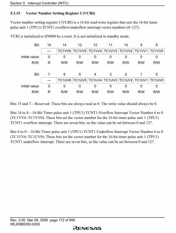
Section 5 Interrupt Controller (INTC)
Rev. 2.00 Mar 09, 2006 page 172 of 906REJ09B0292-0200
5.3.15 Vector Number Setting Register I (VCRI)
Vector number setting register I (VCRI) is a 16-bit read/write register that sets the 16-bit timerpulse unit 1 (TPU1) TCNT1 overflow/underflow interrupt vector numbers (0�127).
VCRI is initialized to H'0000 by a reset. It is not initialized in standby mode.
Bit: 15 14 13 12 11 10 9 8
� TC1VV6 TC1VV5 TC1VV4 TC1VV3 TC1VV2 TC1VV1 TC1VV0
Initial value: 0 0 0 0 0 0 0 0
R/W: R R/W R/W R/W R/W R/W R/W R/W
Bit: 7 6 5 4 3 2 1 0
� TC1UV6 TC1UV5 TC1UV4 TC1UV3 TC1UV2 TC1UV1 TC1UV0
Initial value: 0 0 0 0 0 0 0 0
R/W: R R/W R/W R/W R/W R/W R/W R/W
Bits 15 and 7�Reserved: These bits are always read as 0. The write value should always be 0.
Bits 14 to 8�16-Bit Timer pulse unit 1 (TPU1) TCNT1 Overflow Interrupt Vector Number 6 to 0(TC1VV6�TC1VV0): These bits set the vector number for the 16-bit timer pulse unit 1 (TPU1)TCNT1 overflow interrupt. There are seven bits, so the value can be set between 0 and 127.
Bits 6 to 0�16-Bit Timer pulse unit 1 (TPU1) TCNT1 Underflow Interrupt Vector Number 6 to 0(TC1UV6�TC1UV0): These bits set the vector number for the 16-bit timer pulse unit 1 (TPU1)TCNT1 underflow interrupt. There are seven bits, so the value can be set between 0 and 127.
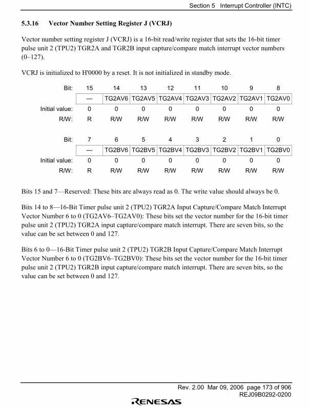
Section 5 Interrupt Controller (INTC)
Rev. 2.00 Mar 09, 2006 page 173 of 906REJ09B0292-0200
5.3.16 Vector Number Setting Register J (VCRJ)
Vector number setting register J (VCRJ) is a 16-bit read/write register that sets the 16-bit timerpulse unit 2 (TPU2) TGR2A and TGR2B input capture/compare match interrupt vector numbers(0�127).
VCRJ is initialized to H'0000 by a reset. It is not initialized in standby mode.
Bit: 15 14 13 12 11 10 9 8
� TG2AV6 TG2AV5 TG2AV4 TG2AV3 TG2AV2 TG2AV1 TG2AV0
Initial value: 0 0 0 0 0 0 0 0
R/W: R R/W R/W R/W R/W R/W R/W R/W
Bit: 7 6 5 4 3 2 1 0
� TG2BV6 TG2BV5 TG2BV4 TG2BV3 TG2BV2 TG2BV1 TG2BV0
Initial value: 0 0 0 0 0 0 0 0
R/W: R R/W R/W R/W R/W R/W R/W R/W
Bits 15 and 7�Reserved: These bits are always read as 0. The write value should always be 0.
Bits 14 to 8�16-Bit Timer pulse unit 2 (TPU2) TGR2A Input Capture/Compare Match InterruptVector Number 6 to 0 (TG2AV6�TG2AV0): These bits set the vector number for the 16-bit timerpulse unit 2 (TPU2) TGR2A input capture/compare match interrupt. There are seven bits, so thevalue can be set between 0 and 127.
Bits 6 to 0�16-Bit Timer pulse unit 2 (TPU2) TGR2B Input Capture/Compare Match InterruptVector Number 6 to 0 (TG2BV6�TG2BV0): These bits set the vector number for the 16-bit timerpulse unit 2 (TPU2) TGR2B input capture/compare match interrupt. There are seven bits, so thevalue can be set between 0 and 127.

Section 5 Interrupt Controller (INTC)
Rev. 2.00 Mar 09, 2006 page 174 of 906REJ09B0292-0200
5.3.17 Vector Number Setting Register K (VCRK)
Vector number setting register K (VCRK) is a 16-bit read/write register that sets the 16-bit timerpulse unit 2 (TPU2) TCNT2 overflow/underflow interrupt vector numbers (0�127).
VCRK is initialized to H'0000 by a reset. It is not initialized in standby mode.
Bit: 15 14 13 12 11 10 9 8
� TC2VV6 TC2VV5 TC2VV4 TC2VV3 TC2VV2 TC2VV1 TC2VV0
Initial value: 0 0 0 0 0 0 0 0
R/W: R R/W R/W R/W R/W R/W R/W R/W
Bit: 7 6 5 4 3 2 1 0
� TC2UV6 TC2UV5 TC2UV4 TC2UV3 TC2UV2 TC2UV1 TC2UV0
Initial value: 0 0 0 0 0 0 0 0
R/W: R R/W R/W R/W R/W R/W R/W R/W
Bits 15 and 7�Reserved: These bits are always read as 0. The write value should always be 0.
Bits 14 to 8�16-Bit Timer pulse unit 2 (TPU2) TCNT2 Overflow Interrupt Vector Number 6 to 0(TC2VV6�TC2VV0): These bits set the vector number for the 16-bit timer pulse unit 2 (TPU2)TCNT2 overflow interrupt. There are seven bits, so the value can be set between 0 and 127.
Bits 6 to 0�16-Bit Timer pulse unit 2 (TPU2) TCNT2 Underflow Interrupt Vector Number 6 to 0(TC2UV6�TC2UV0): These bits set the vector number for the 16-bit timer pulse unit 2 (TPU2)TCNT2 underflow interrupt. There are seven bits, so the value can be set between 0 and 127.
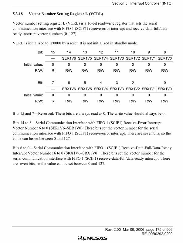
Section 5 Interrupt Controller (INTC)
Rev. 2.00 Mar 09, 2006 page 175 of 906REJ09B0292-0200
5.3.18 Vector Number Setting Register L (VCRL)
Vector number setting register L (VCRL) is a 16-bit read/write register that sets the serialcommunication interface with FIFO 1 (SCIF1) receive-error interrupt and receive-data-full/data-ready interrupt vector numbers (0�127).
VCRL is initialized to H'0000 by a reset. It is not initialized in standby mode.
Bit: 15 14 13 12 11 10 9 8
� SER1V6 SER1V5 SER1V4 SER1V3 SER1V2 SER1V1 SER1V0
Initial value: 0 0 0 0 0 0 0 0
R/W: R R/W R/W R/W R/W R/W R/W R/W
Bit: 7 6 5 4 3 2 1 0
� SRX1V6 SRX1V5 SRX1V4 SRX1V3 SRX1V2 SRX1V1 SRX1V0
Initial value: 0 0 0 0 0 0 0 0
R/W: R R/W R/W R/W R/W R/W R/W R/W
Bits 15 and 7�Reserved: These bits are always read as 0. The write value should always be 0.
Bits 14 to 8�Serial Communication Interface with FIFO 1 (SCIF1) Receive-Error InterruptVector Number 6 to 0 (SER1V6�SER1V0): These bits set the vector number for the serialcommunication interface with FIFO 1 (SCIF1) receive-error interrupt. There are seven bits, so thevalue can be set between 0 and 127.
Bits 6 to 0�Serial Communication Interface with FIFO 1 (SCIF1) Receive-Data-Full/Data-ReadyInterrupt Vector Number 6 to 0 (SRX1V6�SRX1V0): These bits set the vector number for theserial communication interface with FIFO 1 (SCIF1) receive-data-full/data-ready interrupt. Thereare seven bits, so the value can be set between 0 and 127.
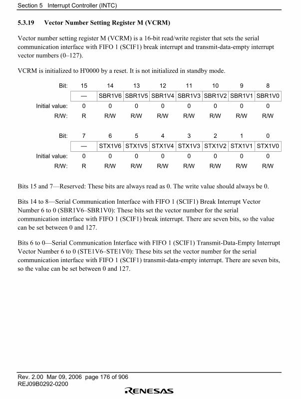
Section 5 Interrupt Controller (INTC)
Rev. 2.00 Mar 09, 2006 page 176 of 906REJ09B0292-0200
5.3.19 Vector Number Setting Register M (VCRM)
Vector number setting register M (VCRM) is a 16-bit read/write register that sets the serialcommunication interface with FIFO 1 (SCIF1) break interrupt and transmit-data-empty interruptvector numbers (0�127).
VCRM is initialized to H'0000 by a reset. It is not initialized in standby mode.
Bit: 15 14 13 12 11 10 9 8
� SBR1V6 SBR1V5 SBR1V4 SBR1V3 SBR1V2 SBR1V1 SBR1V0
Initial value: 0 0 0 0 0 0 0 0
R/W: R R/W R/W R/W R/W R/W R/W R/W
Bit: 7 6 5 4 3 2 1 0
� STX1V6 STX1V5 STX1V4 STX1V3 STX1V2 STX1V1 STX1V0
Initial value: 0 0 0 0 0 0 0 0
R/W: R R/W R/W R/W R/W R/W R/W R/W
Bits 15 and 7�Reserved: These bits are always read as 0. The write value should always be 0.
Bits 14 to 8�Serial Communication Interface with FIFO 1 (SCIF1) Break Interrupt VectorNumber 6 to 0 (SBR1V6�SBR1V0): These bits set the vector number for the serialcommunication interface with FIFO 1 (SCIF1) break interrupt. There are seven bits, so the valuecan be set between 0 and 127.
Bits 6 to 0�Serial Communication Interface with FIFO 1 (SCIF1) Transmit-Data-Empty InterruptVector Number 6 to 0 (STE1V6�STE1V0): These bits set the vector number for the serialcommunication interface with FIFO 1 (SCIF1) transmit-data-empty interrupt. There are seven bits,so the value can be set between 0 and 127.
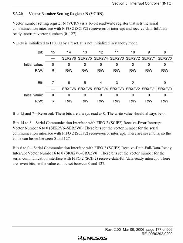
Section 5 Interrupt Controller (INTC)
Rev. 2.00 Mar 09, 2006 page 177 of 906REJ09B0292-0200
5.3.20 Vector Number Setting Register N (VCRN)
Vector number setting register N (VCRN) is a 16-bit read/write register that sets the serialcommunication interface with FIFO 2 (SCIF2) receive-error interrupt and receive-data-full/data-ready interrupt vector numbers (0�127).
VCRN is initialized to H'0000 by a reset. It is not initialized in standby mode.
Bit: 15 14 13 12 11 10 9 8
� SER2V6 SER2V5 SER2V4 SER2V3 SER2V2 SER2V1 SER2V0
Initial value: 0 0 0 0 0 0 0 0
R/W: R R/W R/W R/W R/W R/W R/W R/W
Bit: 7 6 5 4 3 2 1 0
� SRX2V6 SRX2V5 SRX2V4 SRX2V3 SRX2V2 SRX2V1 SRX2V0
Initial value: 0 0 0 0 0 0 0 0
R/W: R R/W R/W R/W R/W R/W R/W R/W
Bits 15 and 7�Reserved: These bits are always read as 0. The write value should always be 0.
Bits 14 to 8�Serial Communication Interface with FIFO 2 (SCIF2) Receive-Error InterruptVector Number 6 to 0 (SER2V6�SER2V0): These bits set the vector number for the serialcommunication interface with FIFO 2 (SCIF2) receive-error interrupt. There are seven bits, so thevalue can be set between 0 and 127.
Bits 6 to 0�Serial Communication Interface with FIFO 2 (SCIF2) Receive-Data-Full/Data-ReadyInterrupt Vector Number 6 to 0 (SRX2V6�SRX2V0): These bits set the vector number for theserial communication interface with FIFO 2 (SCIF2) receive-data-full/data-ready interrupt. Thereare seven bits, so the value can be set between 0 and 127.

Section 5 Interrupt Controller (INTC)
Rev. 2.00 Mar 09, 2006 page 178 of 906REJ09B0292-0200
5.3.21 Vector Number Setting Register O (VCRO)
Vector number setting register O (VCRO) is a 16-bit read/write register that sets the serialcommunication interface with FIFO 2 (SCIF2) break interrupt and transmit-data-empty interruptvector numbers (0�127).
VCRO is initialized to H'0000 by a reset. It is not initialized in standby mode.
Bit: 15 14 13 12 11 10 9 8
� SBR2V6 SBR2V5 SBR2V4 SBR2V3 SBR2V2 SBR2V1 SBR2V0
Initial value: 0 0 0 0 0 0 0 0
R/W: R R/W R/W R/W R/W R/W R/W R/W
Bit: 7 6 5 4 3 2 1 0
� STX2V6 STX2V5 STX2V4 STX2V3 STX2V2 STX2V1 STX2V0
Initial value: 0 0 0 0 0 0 0 0
R/W: R R/W R/W R/W R/W R/W R/W R/W
Bits 15 and 7�Reserved: These bits are always read as 0. The write value should always be 0.
Bits 14 to 8�Serial Communication Interface with FIFO 2 (SCIF2) Break Interrupt VectorNumber 6 to 0 (SBR2V6�SBR2V0): These bits set the vector number for the serialcommunication interface with FIFO 2 (SCIF2) break interrupt. There are seven bits, so the valuecan be set between 0 and 127.
Bits 6 to 0�Serial Communication Interface with FIFO 2 (SCIF2) Transmit-Data-Empty InterruptVector Number 6 to 0 (STE2V6�STE2V0): These bits set the vector number for the serialcommunication interface with FIFO 2 (SCIF2) transmit-data-empty interrupt. There are seven bits,so the value can be set between 0 and 127.

Section 5 Interrupt Controller (INTC)
Rev. 2.00 Mar 09, 2006 page 179 of 906REJ09B0292-0200
5.3.22 Vector Number Setting Register P (VCRP)
Vector number setting register P (VCRP) is a 16-bit read/write register that sets the serial I/O withFIFO (SIOF) receive overrun error interrupt and transmit underrun error interrupt vector numbers(0�127).
VCRP is initialized to H'0000 by a reset. It is not initialized in standby mode.
Bit: 15 14 13 12 11 10 9 8
� RER0V6 RER0V5 RER0V4 RER0V3 RER0V2 RER0V1 RER0V0
Initial value: 0 0 0 0 0 0 0 0
R/W: R R/W R/W R/W R/W R/W R/W R/W
Bit: 7 6 5 4 3 2 1 0
� TER0V6 TER0V5 TER0V4 TER0V3 TER0V2 TER0V1 TER0V0
Initial value: 0 0 0 0 0 0 0 0
R/W: R R/W R/W R/W R/W R/W R/W R/W
Bits 15 and 7�Reserved: These bits are always read as 0. The write value should always be 0.
Bits 14 to 8�Serial I/O with FIFO (SIOF) Receive Overrun Error Interrupt Vector Number 6 to 0(RER0V6�RER0V0): These bits set the vector number for the serial I/O with FIFO (SIOF) receiveoverrun error interrupt. There are seven bits, so the value can be set between 0 and 127.
Bits 6 to 0�Serial I/O with FIFO (SIOF) Transmit Underrun Error Interrupt Vector Number 6 to0 (TER0V6�TER0V0): These bits set the vector number for the serial I/O with FIFO (SIOF)transmit underrun error interrupt. There are seven bits, so the value can be set between 0 and 127.

Section 5 Interrupt Controller (INTC)
Rev. 2.00 Mar 09, 2006 page 180 of 906REJ09B0292-0200
5.3.23 Vector Number Setting Register Q (VCRQ)
Vector number setting register Q (VCRQ) is a 16-bit read/write register that sets the serial I/Owith FIFO (SIOF) receive-data-full interrupt and transmit-data-empty interrupt vector numbers (0�127).
VCRQ is initialized to H'0000 by a reset. It is not initialized in standby mode.
Bit: 15 14 13 12 11 10 9 8
� RDF0V6 RDF0V5 RDF0V4 RDF0V3 RDF0V2 RDF0V1 RDF0V0
Initial value: 0 0 0 0 0 0 0 0
R/W: R R/W R/W R/W R/W R/W R/W R/W
Bit: 7 6 5 4 3 2 1 0
� TDE0V6 TDE0V5 TDE0V4 TDE0V3 TDE0V2 TDE0V1 TDE0V0
Initial value: 0 0 0 0 0 0 0 0
R/W: R R/W R/W R/W R/W R/W R/W R/W
Bits 15 and 7�Reserved: These bits are always read as 0. The write value should always be 0.
Bits 14 to 8�Serial I/O with FIFO (SIOF) Receive-Data-Full Interrupt Vector Number 6 to 0(RDF0V6�RDF0V0): These bits set the vector number for the serial I/O with FIFO (SIOF)receive-data-full interrupt. There are seven bits, so the value can be set between 0 and 127.
Bits 6 to 0�Serial I/O with FIFO (SIOF) Transmit-Data-Empty Interrupt Vector Number 6 to 0(TDE0V6�TDE0V0): These bits set the vector number for the serial I/O with FIFO (SIOF)transmit-data-empty interrupt. There are seven bits, so the value can be set between 0 and 127.
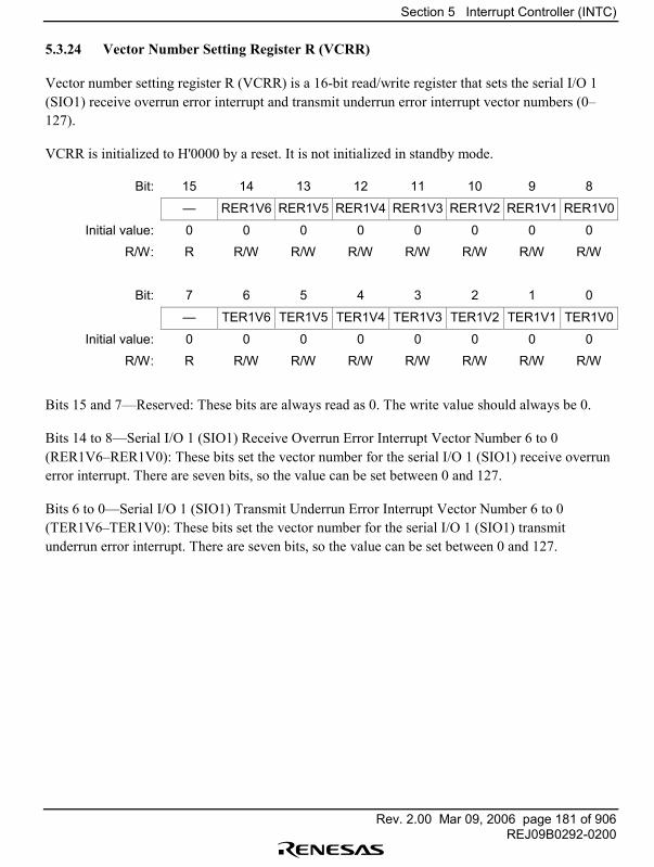
Section 5 Interrupt Controller (INTC)
Rev. 2.00 Mar 09, 2006 page 181 of 906REJ09B0292-0200
5.3.24 Vector Number Setting Register R (VCRR)
Vector number setting register R (VCRR) is a 16-bit read/write register that sets the serial I/O 1(SIO1) receive overrun error interrupt and transmit underrun error interrupt vector numbers (0�127).
VCRR is initialized to H'0000 by a reset. It is not initialized in standby mode.
Bit: 15 14 13 12 11 10 9 8
� RER1V6 RER1V5 RER1V4 RER1V3 RER1V2 RER1V1 RER1V0
Initial value: 0 0 0 0 0 0 0 0
R/W: R R/W R/W R/W R/W R/W R/W R/W
Bit: 7 6 5 4 3 2 1 0
� TER1V6 TER1V5 TER1V4 TER1V3 TER1V2 TER1V1 TER1V0
Initial value: 0 0 0 0 0 0 0 0
R/W: R R/W R/W R/W R/W R/W R/W R/W
Bits 15 and 7�Reserved: These bits are always read as 0. The write value should always be 0.
Bits 14 to 8�Serial I/O 1 (SIO1) Receive Overrun Error Interrupt Vector Number 6 to 0(RER1V6�RER1V0): These bits set the vector number for the serial I/O 1 (SIO1) receive overrunerror interrupt. There are seven bits, so the value can be set between 0 and 127.
Bits 6 to 0�Serial I/O 1 (SIO1) Transmit Underrun Error Interrupt Vector Number 6 to 0(TER1V6�TER1V0): These bits set the vector number for the serial I/O 1 (SIO1) transmitunderrun error interrupt. There are seven bits, so the value can be set between 0 and 127.

Section 5 Interrupt Controller (INTC)
Rev. 2.00 Mar 09, 2006 page 182 of 906REJ09B0292-0200
5.3.25 Vector Number Setting Register S (VCRS)
Vector number setting register S (VCRS) is a 16-bit read/write register that sets the serial I/O 1(SIO1) receive-data-full interrupt and transmit-data-empty interrupt vector numbers (0�127).
VCRS is initialized to H'0000 by a reset. It is not initialized in standby mode.
Bit: 15 14 13 12 11 10 9 8
� RDF1V6 RDF1V5 RDF1V4 RDF1V3 RDF1V2 RDF1V1 RDF1V0
Initial value: 0 0 0 0 0 0 0 0
R/W: R R/W R/W R/W R/W R/W R/W R/W
Bit: 7 6 5 4 3 2 1 0
� TDE1V6 TDE1V5 TDE1V4 TDE1V3 TDE1V2 TDE1V1 TDE1V0
Initial value: 0 0 0 0 0 0 0 0
R/W: R R/W R/W R/W R/W R/W R/W R/W
Bits 15 and 7�Reserved: These bits are always read as 0. The write value should always be 0.
Bits 14 to 8�Serial I/O 1 (SIO1) Receive-Data-Full Interrupt Vector Number 6 to 0 (RDF1V6�RDF1V0): These bits set the vector number for the serial I/O 1 (SIO1) receive-data-full interrupt.There are seven bits, so the value can be set between 0 and 127.
Bits 6 to 0�Serial I/O 1 (SIO1) Transmit-Data-Empty Interrupt Vector Number 6 to 0 (TDE1V6�TDE1V0): These bits set the vector number for the serial I/O 1 (SIO1) transmit-data-emptyinterrupt. There are seven bits, so the value can be set between 0 and 127.
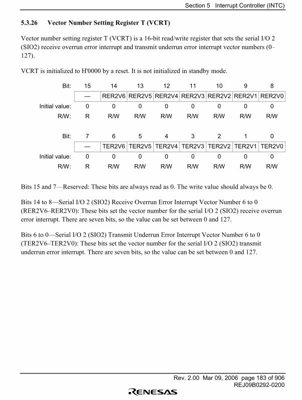
Section 5 Interrupt Controller (INTC)
Rev. 2.00 Mar 09, 2006 page 183 of 906REJ09B0292-0200
5.3.26 Vector Number Setting Register T (VCRT)
Vector number setting register T (VCRT) is a 16-bit read/write register that sets the serial I/O 2(SIO2) receive overrun error interrupt and transmit underrun error interrupt vector numbers (0�127).
VCRT is initialized to H'0000 by a reset. It is not initialized in standby mode.
Bit: 15 14 13 12 11 10 9 8
� RER2V6 RER2V5 RER2V4 RER2V3 RER2V2 RER2V1 RER2V0
Initial value: 0 0 0 0 0 0 0 0
R/W: R R/W R/W R/W R/W R/W R/W R/W
Bit: 7 6 5 4 3 2 1 0
� TER2V6 TER2V5 TER2V4 TER2V3 TER2V2 TER2V1 TER2V0
Initial value: 0 0 0 0 0 0 0 0
R/W: R R/W R/W R/W R/W R/W R/W R/W
Bits 15 and 7�Reserved: These bits are always read as 0. The write value should always be 0.
Bits 14 to 8�Serial I/O 2 (SIO2) Receive Overrun Error Interrupt Vector Number 6 to 0(RER2V6�RER2V0): These bits set the vector number for the serial I/O 2 (SIO2) receive overrunerror interrupt. There are seven bits, so the value can be set between 0 and 127.
Bits 6 to 0�Serial I/O 2 (SIO2) Transmit Underrun Error Interrupt Vector Number 6 to 0(TER2V6�TER2V0): These bits set the vector number for the serial I/O 2 (SIO2) transmitunderrun error interrupt. There are seven bits, so the value can be set between 0 and 127.
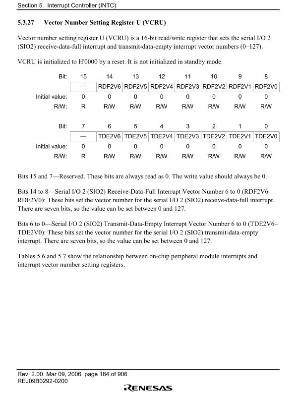
Section 5 Interrupt Controller (INTC)
Rev. 2.00 Mar 09, 2006 page 184 of 906REJ09B0292-0200
5.3.27 Vector Number Setting Register U (VCRU)
Vector number setting register U (VCRU) is a 16-bit read/write register that sets the serial I/O 2(SIO2) receive-data-full interrupt and transmit-data-empty interrupt vector numbers (0�127).
VCRU is initialized to H'0000 by a reset. It is not initialized in standby mode.
Bit: 15 14 13 12 11 10 9 8
� RDF2V6 RDF2V5 RDF2V4 RDF2V3 RDF2V2 RDF2V1 RDF2V0
Initial value: 0 0 0 0 0 0 0 0
R/W: R R/W R/W R/W R/W R/W R/W R/W
Bit: 7 6 5 4 3 2 1 0
� TDE2V6 TDE2V5 TDE2V4 TDE2V3 TDE2V2 TDE2V1 TDE2V0
Initial value: 0 0 0 0 0 0 0 0
R/W: R R/W R/W R/W R/W R/W R/W R/W
Bits 15 and 7�Reserved. These bits are always read as 0. The write value should always be 0.
Bits 14 to 8�Serial I/O 2 (SIO2) Receive-Data-Full Interrupt Vector Number 6 to 0 (RDF2V6�RDF2V0): These bits set the vector number for the serial I/O 2 (SIO2) receive-data-full interrupt.There are seven bits, so the value can be set between 0 and 127.
Bits 6 to 0�Serial I/O 2 (SIO2) Transmit-Data-Empty Interrupt Vector Number 6 to 0 (TDE2V6�TDE2V0): These bits set the vector number for the serial I/O 2 (SIO2) transmit-data-emptyinterrupt. There are seven bits, so the value can be set between 0 and 127.
Tables 5.6 and 5.7 show the relationship between on-chip peripheral module interrupts andinterrupt vector number setting registers.
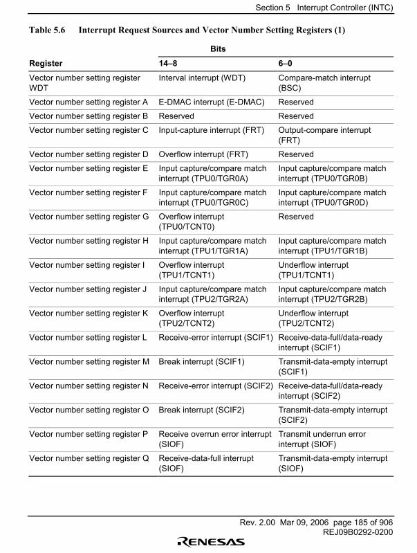
Section 5 Interrupt Controller (INTC)
Rev. 2.00 Mar 09, 2006 page 185 of 906REJ09B0292-0200
Table 5.6 Interrupt Request Sources and Vector Number Setting Registers (1)
Bits
Register 14�8 6�0
Vector number setting registerWDT
Interval interrupt (WDT) Compare-match interrupt(BSC)
Vector number setting register A E-DMAC interrupt (E-DMAC) Reserved
Vector number setting register B Reserved Reserved
Vector number setting register C Input-capture interrupt (FRT) Output-compare interrupt(FRT)
Vector number setting register D Overflow interrupt (FRT) Reserved
Vector number setting register E Input capture/compare matchinterrupt (TPU0/TGR0A)
Input capture/compare matchinterrupt (TPU0/TGR0B)
Vector number setting register F Input capture/compare matchinterrupt (TPU0/TGR0C)
Input capture/compare matchinterrupt (TPU0/TGR0D)
Vector number setting register G Overflow interrupt(TPU0/TCNT0)
Reserved
Vector number setting register H Input capture/compare matchinterrupt (TPU1/TGR1A)
Input capture/compare matchinterrupt (TPU1/TGR1B)
Vector number setting register I Overflow interrupt(TPU1/TCNT1)
Underflow interrupt(TPU1/TCNT1)
Vector number setting register J Input capture/compare matchinterrupt (TPU2/TGR2A)
Input capture/compare matchinterrupt (TPU2/TGR2B)
Vector number setting register K Overflow interrupt(TPU2/TCNT2)
Underflow interrupt(TPU2/TCNT2)
Vector number setting register L Receive-error interrupt (SCIF1) Receive-data-full/data-readyinterrupt (SCIF1)
Vector number setting register M Break interrupt (SCIF1) Transmit-data-empty interrupt(SCIF1)
Vector number setting register N Receive-error interrupt (SCIF2) Receive-data-full/data-readyinterrupt (SCIF2)
Vector number setting register O Break interrupt (SCIF2) Transmit-data-empty interrupt(SCIF2)
Vector number setting register P Receive overrun error interrupt(SIOF)
Transmit underrun errorinterrupt (SIOF)
Vector number setting register Q Receive-data-full interrupt(SIOF)
Transmit-data-empty interrupt(SIOF)
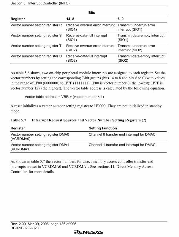
Section 5 Interrupt Controller (INTC)
Rev. 2.00 Mar 09, 2006 page 186 of 906REJ09B0292-0200
Bits
Register 14�8 6�0
Vector number setting register R Receive overrun error interrupt(SIO1)
Transmit underrun errorinterrupt (SIO1)
Vector number setting register S Receive-data-full interrupt(SIO1)
Transmit-data-empty interrupt(SIO1)
Vector number setting register T Receive overrun error interrupt(SIO2)
Transmit underrun errorinterrupt (SIO2)
Vector number setting register U Receive-data-full interrupt(SIO2)
Transmit-data-empty interrupt(SIO2)
As table 5.6 shows, two on-chip peripheral module interrupts are assigned to each register. Set thevector numbers by setting the corresponding 7-bit groups (bits 14 to 8 and bits 6 to 0) with valuesin the range of H'00 (0000000) to H'7F (1111111). H'00 is vector number 0 (the lowest); H'7F isvector number 127 (the highest). The vector table address is calculated by the following equation.
Vector table address = VBR + (vector number × 4)
A reset initializes a vector number setting register to H'0000. They are not initialized in standbymode.
Table 5.7 Interrupt Request Sources and Vector Number Setting Registers (2)
Register Setting Function
Vector number setting register DMA0(VCRDMA0)
Channel 0 transfer end interrupt for DMAC
Vector number setting register DMA1(VCRDMA1)
Channel 1 transfer end interrupt for DMAC
As shown in table 5.7 the vector numbers for direct memory access controller transfer-endinterrupts are set in VCRDMA0 and VCRDMA1. See sections 11, Direct Memory AccessController, for more details.
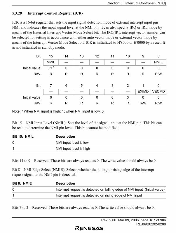
Section 5 Interrupt Controller (INTC)
Rev. 2.00 Mar 09, 2006 page 187 of 906REJ09B0292-0200
5.3.28 Interrupt Control Register (ICR)
ICR is a 16-bit register that sets the input signal detection mode of external interrupt input pinNMI and indicates the input signal level at the NMI pin. It can also specify IRQ or IRL mode bymeans of the External Interrupt Vector Mode Select bit. The IRQ/IRL interrupt vector number canbe selected for setting in accordance with either auto vector mode or external vector mode bymeans of the Interrupt Vector Mode Select bit. ICR is initialized to H'8000 or H'0000 by a reset. Itis not initialized in standby mode.
Bit: 15 14 13 12 11 10 9 8
NMIL � � � � � � NMIE
Initial value: 0/1* 0 0 0 0 0 0 0
R/W: R R R R R R R R/W
Bit: 7 6 5 4 3 2 1 0
� � � � � � EXIMD VECMD
Initial value: 0 0 0 0 0 0 0 0
R/W: R R R R R R R/W R/W
Note: * When NMI input is high: 1; when NMI input is low: 0
Bit 15�NMI Input Level (NMIL): Sets the level of the signal input at the NMI pin. This bit canbe read to determine the NMI pin level. This bit cannot be modified.
Bit 15: NMIL Description
0 NMI input level is low
1 NMI input level is high
Bits 14 to 9�Reserved: These bits are always read as 0. The write value should always be 0.
Bit 8�NMI Edge Select (NMIE): Selects whether the falling or rising edge of the interruptrequest signal to the NMI pin is detected.
Bit 8: NMIE Description
0 Interrupt request is detected on falling edge of NMI input (Initial value)
1 Interrupt request is detected on rising edge of NMI input
Bits 7 to 2�Reserved: These bits are always read as 0. The write value should always be 0.
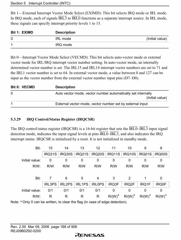
Section 5 Interrupt Controller (INTC)
Rev. 2.00 Mar 09, 2006 page 188 of 906REJ09B0292-0200
Bit 1�External Interrupt Vector Mode Select (EXIMD): This bit selects IRQ mode or IRL mode.In IRQ mode, each of signals IRL3 to IRL0 functions as a separate interrupt source. In IRL mode,these signals can specify interrupt priority levels 1 to 15.
Bit 1: EXIMD Description
0 IRL mode (Initial value)
1 IRQ mode
Bit 0�Interrupt Vector Mode Select (VECMD): This bit selects auto-vector mode or externalvector mode for IRL/IRQ interrupt vector number setting. In auto-vector mode, an internallydetermined vector number is set. The IRL15 and IRL14 interrupt vector numbers are set to 71 andthe IRL1 vector number is set to 64. In external vector mode, a value between 0 and 127 can beinput as the vector number from the external vector number input pins (D7�D0).
Bit 0: VECMD Description
0 Auto vector mode, vector number automatically set internally(Initial value)
1 External vector mode, vector number set by external input
5.3.29 IRQ Control/Status Register (IRQCSR)
The IRQ control/status register (IRQCSR) is a 16-bit register that sets the IRL0�IRL3 input signaldetection mode, indicates the input signal levels at pins IRL0�IRL3, and also indicates the IRQinterrupt status. IRQCSR is initialized by a reset. It is not initialized in standby mode.
Bit: 15 14 13 12 11 10 9 8
IRQ31S IRQ30S IRQ21S IRQ20S IRQ11S IRQ10S IRQ01S IRQ00S
Initial value: 0 0 0 0 0 0 0 0
R/W: R/W R/W R/W R/W R/W R/W R/W R/W
Bit: 7 6 5 4 3 2 1 0
IRL3PS IRL2PS IRL1PS IRL0PS IRQ3F IRQ2F IRQ1F IRQ0F
Initial value: 0/1 0/1 0/1 0/1 0 0 0 0
R/W: R R R R R/(W)* R/(W)* R/(W)* R/(W)*
Note: * Only 0 can be written, to clear the flag (in case of edge detection).
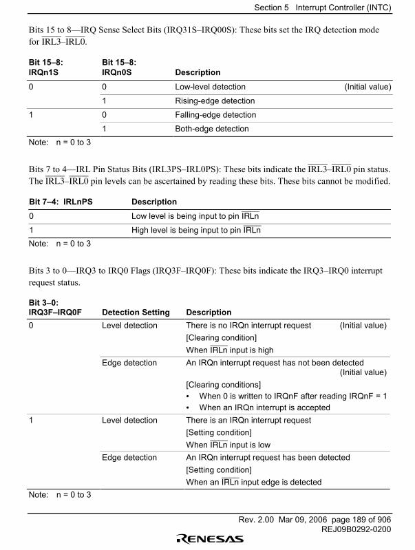
Section 5 Interrupt Controller (INTC)
Rev. 2.00 Mar 09, 2006 page 189 of 906REJ09B0292-0200
Bits 15 to 8�IRQ Sense Select Bits (IRQ31S�IRQ00S): These bits set the IRQ detection modefor IRL3�IRL0.
Bit 15�8:IRQn1S
Bit 15�8:IRQn0S Description
0 0 Low-level detection (Initial value)
1 Rising-edge detection
1 0 Falling-edge detection
1 Both-edge detectionNote: n = 0 to 3
Bits 7 to 4�IRL Pin Status Bits (IRL3PS�IRL0PS): These bits indicate the IRL3�IRL0 pin status.The IRL3�IRL0 pin levels can be ascertained by reading these bits. These bits cannot be modified.
Bit 7�4: IRLnPS Description
0 Low level is being input to pin IRLn
1 High level is being input to pin IRLnNote: n = 0 to 3
Bits 3 to 0�IRQ3 to IRQ0 Flags (IRQ3F�IRQ0F): These bits indicate the IRQ3�IRQ0 interruptrequest status.
Bit 3�0:IRQ3F�IRQ0F Detection Setting Description0 Level detection There is no IRQn interrupt request (Initial value)
[Clearing condition]When IRLn input is high
Edge detection An IRQn interrupt request has not been detected(Initial value)
[Clearing conditions]• When 0 is written to IRQnF after reading IRQnF = 1• When an IRQn interrupt is accepted
1 Level detection There is an IRQn interrupt request[Setting condition]When IRLn input is low
Edge detection An IRQn interrupt request has been detected[Setting condition]When an IRLn input edge is detected
Note: n = 0 to 3
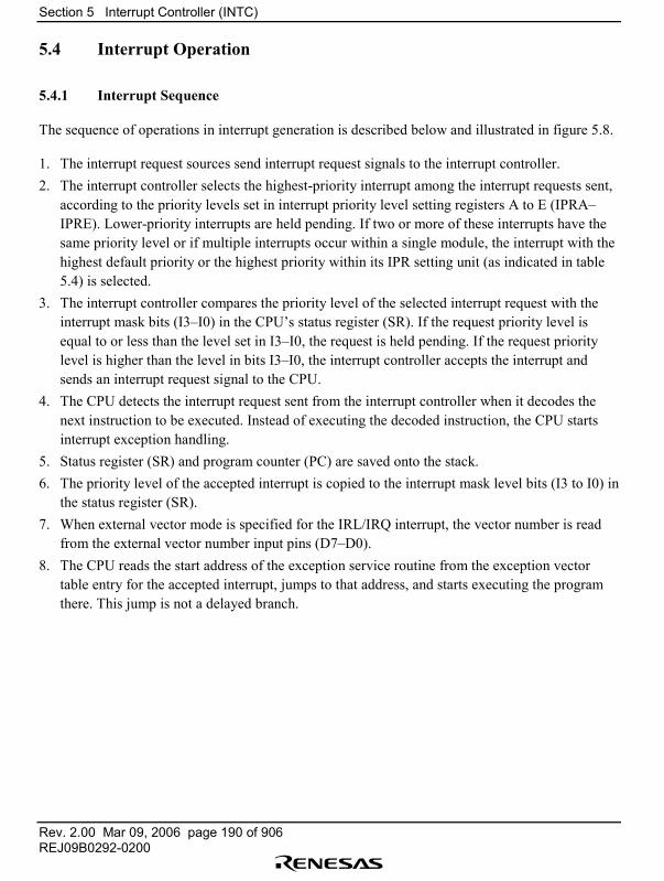
Section 5 Interrupt Controller (INTC)
Rev. 2.00 Mar 09, 2006 page 190 of 906REJ09B0292-0200
5.4 Interrupt Operation
5.4.1 Interrupt Sequence
The sequence of operations in interrupt generation is described below and illustrated in figure 5.8.
1. The interrupt request sources send interrupt request signals to the interrupt controller.2. The interrupt controller selects the highest-priority interrupt among the interrupt requests sent,
according to the priority levels set in interrupt priority level setting registers A to E (IPRA�IPRE). Lower-priority interrupts are held pending. If two or more of these interrupts have thesame priority level or if multiple interrupts occur within a single module, the interrupt with thehighest default priority or the highest priority within its IPR setting unit (as indicated in table5.4) is selected.
3. The interrupt controller compares the priority level of the selected interrupt request with theinterrupt mask bits (I3�I0) in the CPU�s status register (SR). If the request priority level isequal to or less than the level set in I3�I0, the request is held pending. If the request prioritylevel is higher than the level in bits I3�I0, the interrupt controller accepts the interrupt andsends an interrupt request signal to the CPU.
4. The CPU detects the interrupt request sent from the interrupt controller when it decodes thenext instruction to be executed. Instead of executing the decoded instruction, the CPU startsinterrupt exception handling.
5. Status register (SR) and program counter (PC) are saved onto the stack.6. The priority level of the accepted interrupt is copied to the interrupt mask level bits (I3 to I0) in
the status register (SR).7. When external vector mode is specified for the IRL/IRQ interrupt, the vector number is read
from the external vector number input pins (D7�D0).8. The CPU reads the start address of the exception service routine from the exception vector
table entry for the accepted interrupt, jumps to that address, and starts executing the programthere. This jump is not a delayed branch.
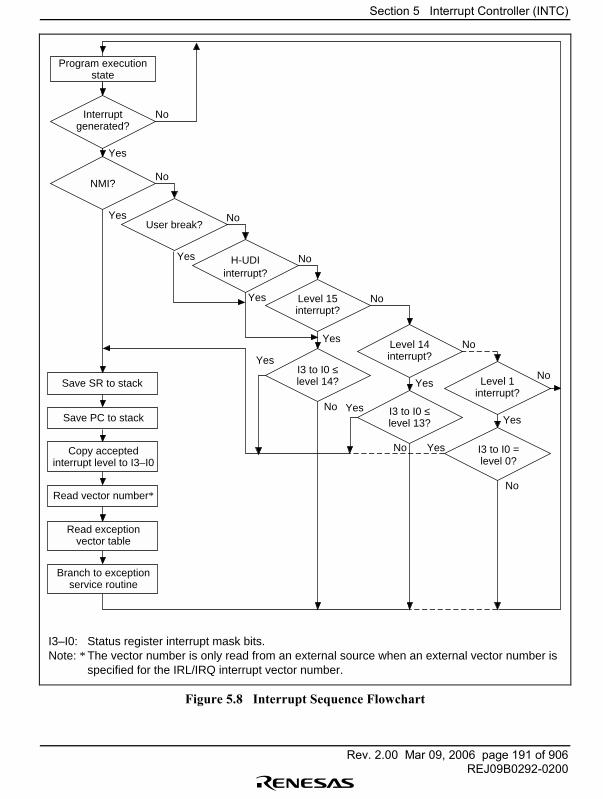
Section 5 Interrupt Controller (INTC)
Rev. 2.00 Mar 09, 2006 page 191 of 906REJ09B0292-0200
No
Yes
NMI?No
YesUser break?
NoYes
No
H-UDIinterrupt?
Yes Level 15interrupt?
No
Yes
I3 to I0 ≤level 14?
No
Yes
Level 14interrupt?
No
Yes
Yes
I3 to I0 ≤level 13?
No
Yes
Level 1interrupt?
No
Yes
I3 to I0 =level 0?
No
Program executionstate
Save SR to stack
Save PC to stack
Read vector number*
Branch to exceptionservice routine
Interruptgenerated?
Copy acceptedinterrupt level to I3–I0
Read exceptionvector table
I3–I0: Status register interrupt mask bits.Note: * The vector number is only read from an external source when an external vector number is specified for the IRL/IRQ interrupt vector number.
Figure 5.8 Interrupt Sequence Flowchart
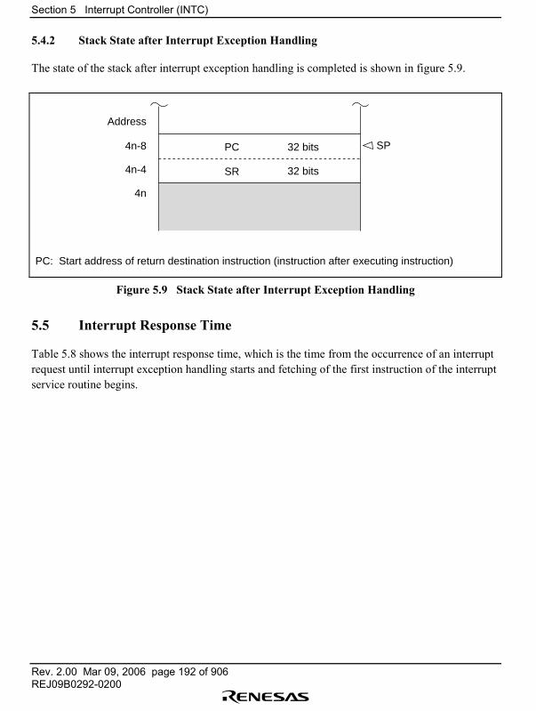
Section 5 Interrupt Controller (INTC)
Rev. 2.00 Mar 09, 2006 page 192 of 906REJ09B0292-0200
5.4.2 Stack State after Interrupt Exception Handling
The state of the stack after interrupt exception handling is completed is shown in figure 5.9.
Address
4n-8
4n-4
4n
PC
PC: Start address of return destination instruction (instruction after executing instruction)
SP32 bits
32 bitsSR
Figure 5.9 Stack State after Interrupt Exception Handling
5.5 Interrupt Response Time
Table 5.8 shows the interrupt response time, which is the time from the occurrence of an interruptrequest until interrupt exception handling starts and fetching of the first instruction of the interruptservice routine begins.
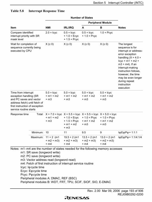
Section 5 Interrupt Controller (INTC)
Rev. 2.00 Mar 09, 2006 page 193 of 906REJ09B0292-0200
Table 5.8 Interrupt Response Time
Number of States
Peripheral Module
Item NMI IRL/IRQ A B Notes
Compare identifiedinterrupt priority with SRmask level
2.0 × Icyc 0.5 × Icyc+ 1.0 × Ecyc+ 1.5 × Pcyc
0.5 × Icyc+ 1.0 × Pcyc
1.0 × Pcyc
Wait for completion ofsequence currently beingexecuted by CPU
X (≥ 0) X (≥ 0) X (≥ 0) X (≥ 0) The longestsequence is forinterrupt or address-error exceptionhandling (X = 4.0 ×Icyc + m1 + m2 +m3 + m4). If aninterrupt-makinginstruction follows,however, the timemay be even longerduring repeatinstructionexecution
Time from interruptexception handling (SRand PC saves and vectoraddress fetch) until fetch offirst instruction of exceptionservice routine starts
5.0 × Icyc+ m1 + m2+ m3
5.0 × Icyc+ m1 + m2+ m3
5.0 × Icyc+ m1 + m2+ m3
5.0 × Icyc+ m1 + m2+ m3
Response time Total: X + 7.0 × Icyc+ m1 + m2+ m3
X + 5.5 × Icyc+ 1.0 × Ecyc+ 1.5 × Pcyc+ m1 + m2+ m3
X + 5.5 × Icyc+ 1.0 × Pcyc+ m1 + m2+ m3
X + 5.0 × Icyc+ 1.0 × Pcyc+ m1 + m2+ m3
Minimum: 10 11 9.5 9 Iφ:Eφ:Pφ = 1:1:1
Maximum: 11 + 2 (m1+ m2 + m3)+ m4
19.5 + 2 (m1+ m2 + m3)+ m4
13.5 + 2 (m1+ m2 + m3)+ m4
13.0 + 2 (m1+ m2 + m3)+ m4
Iφ:Eφ:Pφ = 1:1/4:1/4
Notes: m1�m4 are the number of states needed for the following memory accessesm1: SR save (longword write)m2: PC save (longword write)m3: Vector address read (longword read)m4: Fetch of first instruction of interrupt service routineIcyc: Iφ cycle timeEcyc: Eφ cycle timePcyc: Pφ cycle timePeripheral modules A: DMAC, REF (BSC)Peripheral modules B: WDT, FRT, TPU, SCIF, SIOF, SIO, E-DMAC
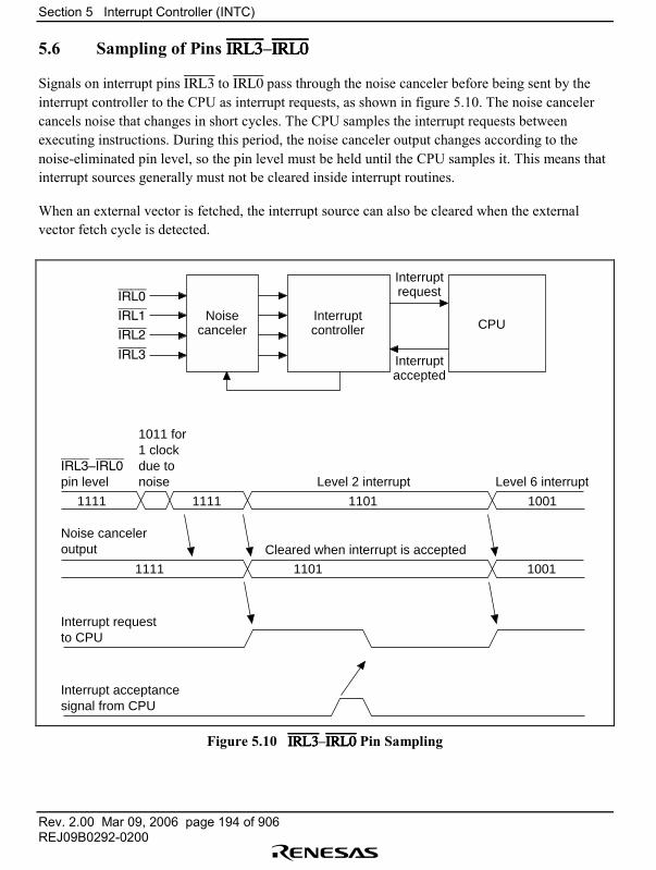
Section 5 Interrupt Controller (INTC)
Rev. 2.00 Mar 09, 2006 page 194 of 906REJ09B0292-0200
5.6 Sampling of Pins IRL3IRL3IRL3IRL3�IRL0IRL0IRL0IRL0
Signals on interrupt pins IRL3 to IRL0 pass through the noise canceler before being sent by theinterrupt controller to the CPU as interrupt requests, as shown in figure 5.10. The noise cancelercancels noise that changes in short cycles. The CPU samples the interrupt requests betweenexecuting instructions. During this period, the noise canceler output changes according to thenoise-eliminated pin level, so the pin level must be held until the CPU samples it. This means thatinterrupt sources generally must not be cleared inside interrupt routines.
When an external vector is fetched, the interrupt source can also be cleared when the externalvector fetch cycle is detected.
Interrupt acceptancesignal from CPU
Interrupt requestto CPU
Noise canceleroutput
Cleared when interrupt is accepted
IRL3–IRL0
pin level
1011 for 1 clock due to noise Level 2 interrupt Level 6 interrupt
1111
1111 1101 1001
1111 1101 1001
IRL0
IRL1
IRL2
IRL3
CPUInterruptcontroller
Noisecanceler
Interruptrequest
Interruptaccepted
Figure 5.10 IRL3IRL3IRL3IRL3�IRL0IRL0IRL0IRL0 Pin Sampling
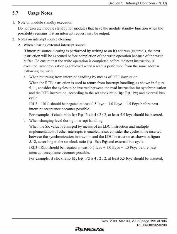
Section 5 Interrupt Controller (INTC)
Rev. 2.00 Mar 09, 2006 page 195 of 906REJ09B0292-0200
5.7 Usage Notes
1. Note on module standby executionDo not execute module standby for modules that have the module standby function when thepossibility remains that an interrupt request may be output.
2. Notes on interrupt source clearingA. When clearing external interrupt source
If interrupt source clearing is performed by writing to an IO address (external), the nextinstruction will be executed before completion of the write operation because of the writebuffer. To ensure that the write operation is completed before the next instruction isexecuted, synchronization is achieved when a read is performed from the same addressfollowing the write.a. When returning from interrupt handling by means of RTE instruction
When the RTE instruction is used to return from interrupt handling, as shown in figure5.11, consider the cycles to be inserted between the read instruction for synchronizationand the RTE instruction, according to the set clock ratio (Iφ : Eφ : Pφ) and external buscycle.IRL3�IRL0 should be negated at least 0.5 Icyc + 1.0 Ecyc + 1.5 Pcyc before nextinterrupt acceptance becomes possible.For example, if clock ratio Iφ : Eφ : Pφ is 4 : 2 : 2, at least 5.5 Icyc should be inserted.
b. When changing level during interrupt handlingWhen the SR value is changed by means of an LDC instruction and multipleimplementation of other interrupts is enabled, also, consider the cycles to be insertedbetween the synchronization instruction and the LDC instruction as shown in figure5.12, according to the set clock ratio (Iφ : Eφ : Pφ) and external bus cycle.IRL3�IRL0 should be negated at least 0.5 Icyc + 1.0 Ecyc + 1.5 Pcyc before nextinterrupt acceptance becomes possible.For example, if clock ratio Iφ : Eφ : Pφ is 4 : 2 : 2, at least 5.5 Icyc should be inserted.
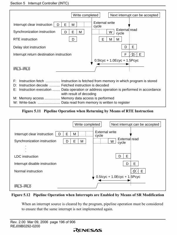
Section 5 Interrupt Controller (INTC)
Rev. 2.00 Mar 09, 2006 page 196 of 906REJ09B0292-0200
Interrupt clear instruction External write cycle
External read cycle
Write completed Next interrupt can be accepted
Synchronization instruction
RTE instruction
IRL3–IRL0
Delay slot instruction
Interrupt return destination instruction
D E M
MD E
ME M
W
D E
EF D
D
0.5Icyc + 1.0Ecyc + 1.5Pcyc
F: Instruction fetch ............... Instruction is fetched from memory in which program is storedD: Instruction decode ........... Fetched instruction is decodedE: Instruction execution ........ Data operation or address operation is performed in accordance with result of decodingM: Memory access ................ Memory data access is performedW: Write-back ....................... Data read from memory is written to register
Figure 5.11 Pipeline Operation when Returning by Means of RTE Instruction
Interrupt clear instructionExternal write cycle
External read cycle
Write completed Next interrupt can be accepted
Synchronization instruction•
•
•
IRL3–IRL0
LDC instruction
Interrupt disable instruction
Normal instruction
D E M
MD E W
D E
D E
D E
0.5Icyc + 1.0Ecyc + 1.5Pcyc
Figure 5.12 Pipeline Operation when Interrupts are Enabled by Means of SR Modification
When an interrupt source is cleared by the program, pipeline operation must be consideredto ensure that the same interrupt is not implemented again.
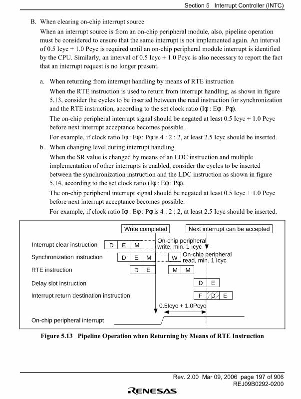
Section 5 Interrupt Controller (INTC)
Rev. 2.00 Mar 09, 2006 page 197 of 906REJ09B0292-0200
B. When clearing on-chip interrupt sourceWhen an interrupt source is from an on-chip peripheral module, also, pipeline operationmust be considered to ensure that the same interrupt is not implemented again. An intervalof 0.5 Icyc + 1.0 Pcyc is required until an on-chip peripheral module interrupt is identifiedby the CPU. Similarly, an interval of 0.5 Icyc + 1.0 Pcyc is also necessary to report the factthat an interrupt request is no longer present.
a. When returning from interrupt handling by means of RTE instructionWhen the RTE instruction is used to return from interrupt handling, as shown in figure5.13, consider the cycles to be inserted between the read instruction for synchronizationand the RTE instruction, according to the set clock ratio (Iφ : Eφ : Pφ).The on-chip peripheral interrupt signal should be negated at least 0.5 Icyc + 1.0 Pcycbefore next interrupt acceptance becomes possible.For example, if clock ratio Iφ : Eφ : Pφ is 4 : 2 : 2, at least 2.5 Icyc should be inserted.
b. When changing level during interrupt handlingWhen the SR value is changed by means of an LDC instruction and multipleimplementation of other interrupts is enabled, consider the cycles to be insertedbetween the synchronization instruction and the LDC instruction as shown in figure5.14, according to the set clock ratio (Iφ : Eφ : Pφ).The on-chip peripheral interrupt signal should be negated at least 0.5 Icyc + 1.0 Pcycbefore next interrupt acceptance becomes possible.For example, if clock ratio Iφ : Eφ : Pφ is 4 : 2 : 2, at least 2.5 Icyc should be inserted.
Interrupt clear instructionOn-chip peripheral write, min. 1 Icyc
Write completed Next interrupt can be accepted
Synchronization instruction
RTE instruction
On-chip peripheral interrupt
Delay slot instruction
Interrupt return destination instruction
D E M
M
E
D E
M M
W
D E
EF D
D
0.5Icyc + 1.0Pcyc
On-chip peripheral read, min. 1 Icyc
Figure 5.13 Pipeline Operation when Returning by Means of RTE Instruction
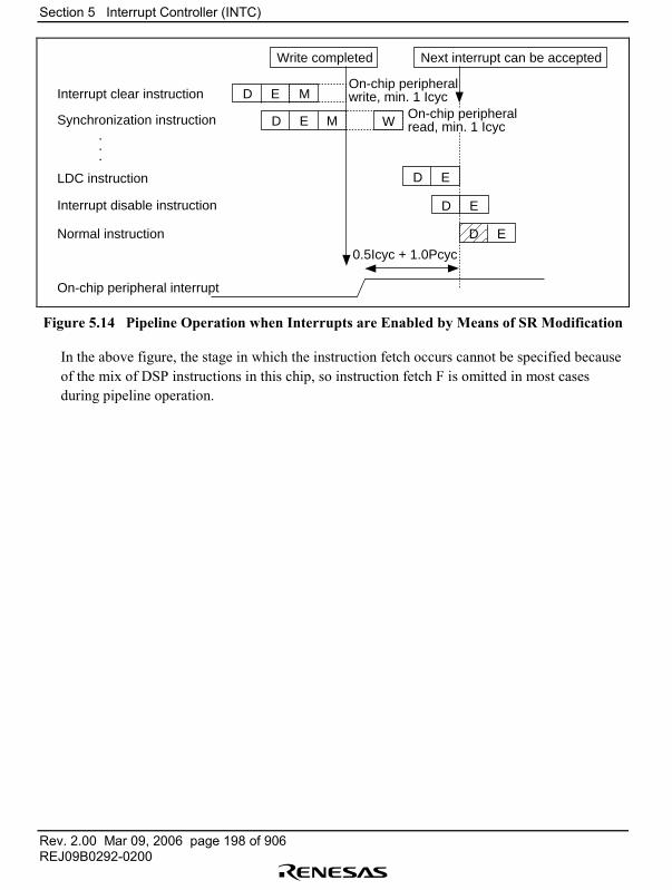
Section 5 Interrupt Controller (INTC)
Rev. 2.00 Mar 09, 2006 page 198 of 906REJ09B0292-0200
Interrupt clear instructionOn-chip peripheral write, min. 1 Icyc
Write completed Next interrupt can be accepted
Synchronization instruction•
•
•
On-chip peripheral interrupt
LDC instruction
Interrupt disable instruction
Normal instruction
D E M
MD E W
D E
D E
D E
0.5Icyc + 1.0Pcyc
On-chip peripheral read, min. 1 Icyc
Figure 5.14 Pipeline Operation when Interrupts are Enabled by Means of SR Modification
In the above figure, the stage in which the instruction fetch occurs cannot be specified becauseof the mix of DSP instructions in this chip, so instruction fetch F is omitted in most casesduring pipeline operation.
Section 6 User Break Controller (UBC)
Rev. 2.00 Mar 09, 2006 page 199 of 906REJ09B0292-0200
Section 6 User Break Controller (UBC)
6.1 Overview
The user break controller (UBC) provides functions that simplify program debugging. When breakconditions are set in the UBC, a user break interrupt is generated according to the conditions of thebus cycle generated by the CPU or on-chip DMAC (DMAC or E-DMAC).
This function makes it easy to design a sophisticated self-monitoring debugger, enabling programsto be debugged with the chip alone, without using an in-circuit emulator.
6.1.1 Features
The UBC has the following features:
• The following can be set as break conditions: Number of break channels: Four (channels A, B, C, and D)
User break interrupts can be generated on independent or sequential conditions forchannels A, B, C, and D.
Sequential break settings• Channel A → channel B → channel C → channel D• Channel B → channel C → channel D• Channel C → channel D
1. Address: 32-bit masking capability, individual address setting possible (cache bus (CPU),internal bus (DMAC, E-DMAC), X/Y bus)
2. Data (channels C and D only,): 32-bit masking capability, individual address settingpossible (cache bus (CPU), internal bus (DMAC, E-DMAC), X/Y bus)
3. Bus master: CPU cycle/on-chip DMAC (DMAC, E-DMAC) cycle4. Bus cycle: Instruction fetch/data access5. Read/write6. Operand cycle: Byte/word/longword
• User break interrupt generation on occurrence of break conditionA user-written user break interrupt exception routine can be executed.
• Processing can be stopped before or after instruction execution in an instruction fetch cycle.• Break with specification of number of executions (channels C and D only)
Settable number of executions: maximum 212 � 1 (4095)• PC trace function
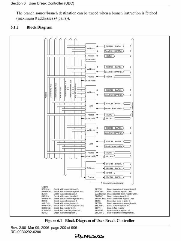
Section 6 User Break Controller (UBC)
Rev. 2.00 Mar 09, 2006 page 200 of 906REJ09B0292-0200
The branch source/branch destination can be traced when a branch instruction is fetched(maximum 8 addresses (4 pairs)).
6.1.2 Block Diagram
Address
Access
Channel A
Address
Access
Channel B
Address
Data
Access
Channel C
Address
Data
Access
PC trace
Control
Channel D
BARAH BARAL
BAMRAH BAMRAL
BBRA
BARBH BARBL
BAMRBH BAMRBL
BARCH BARCL
BAMRCH BAMRCL
BDRCH
BBRC
BETRC
BDRCL
BDMRCH BDMRCL
BARDH BARDL
BAMRDH BAMRDL
BDRDH
BBRD
BETRD
BDRDL
BRSRH BRSRL
BRDRH BRDRL
BRFR
BRCRH BRCRL
BDMRDH BDMRDL
BBRB
Acc
ess
Mod
ule
data
bus
Cac
he d
ata
bus
Inte
rnal
dat
a bu
s
X/Y
dat
a bu
s
Cac
he a
ddre
ss b
us
Inte
rnal
add
ress
bus
X/Y
add
ress
bus
Internal interrupt signal
LegendBARAH/L: Break address register AH/LBAMRAH/L: Break address mask register AH/LBBRA: Break bus cycle register ABARBH/L: Break address register BH/LBAMRBH/L: Break address mask register BH/LBBRB: Break bus cycle register BBARCH/L: Break address register CH/LBAMRCH/L: Break address mask register CH/LBDRCH/L: Break data register CH/LBDMRCH/L: Break data mask register CH/LBBRC: Break bus cycle register C
BETRC: Break execution times register CBARDH/L: Break address register DH/LBAMRDH/L: Break address mask register DH/LBDRDH/L: Break data register DH/LBDMRDH/L: Break data mask register DH/LBBRD: Break bus cycle register DBETRD: Break execution times register DBRCRH/L: Break control register H/LBRFR: Branch flag registerBRSRH/L: Branch source register H/LBRDRH/L: Branch destination register H/L
Figure 6.1 Block Diagram of User Break Controller
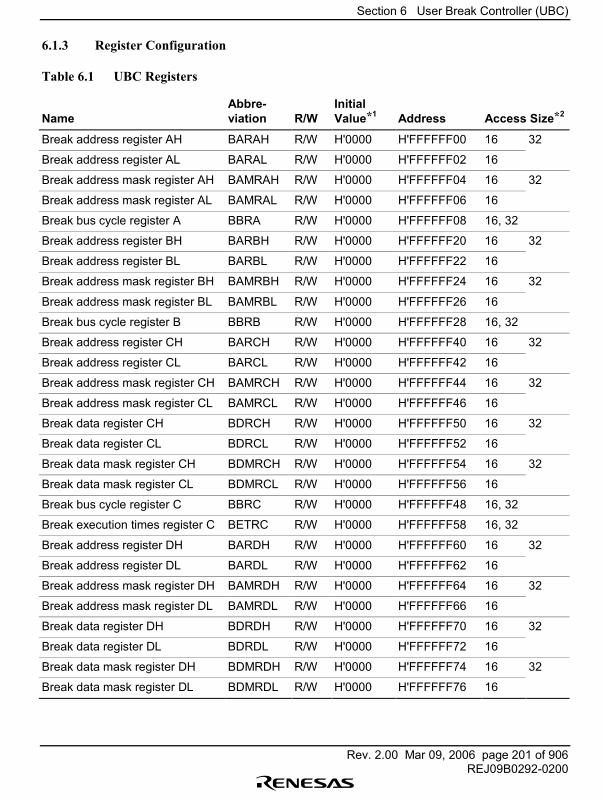
Section 6 User Break Controller (UBC)
Rev. 2.00 Mar 09, 2006 page 201 of 906REJ09B0292-0200
6.1.3 Register Configuration
Table 6.1 UBC Registers
NameAbbre-viation R/W
InitialValue*1 Address Access Size*2
Break address register AH BARAH R/W H'0000 H'FFFFFF00 16 32
Break address register AL BARAL R/W H'0000 H'FFFFFF02 16
Break address mask register AH BAMRAH R/W H'0000 H'FFFFFF04 16 32
Break address mask register AL BAMRAL R/W H'0000 H'FFFFFF06 16
Break bus cycle register A BBRA R/W H'0000 H'FFFFFF08 16, 32
Break address register BH BARBH R/W H'0000 H'FFFFFF20 16 32
Break address register BL BARBL R/W H'0000 H'FFFFFF22 16
Break address mask register BH BAMRBH R/W H'0000 H'FFFFFF24 16 32
Break address mask register BL BAMRBL R/W H'0000 H'FFFFFF26 16
Break bus cycle register B BBRB R/W H'0000 H'FFFFFF28 16, 32
Break address register CH BARCH R/W H'0000 H'FFFFFF40 16 32
Break address register CL BARCL R/W H'0000 H'FFFFFF42 16
Break address mask register CH BAMRCH R/W H'0000 H'FFFFFF44 16 32
Break address mask register CL BAMRCL R/W H'0000 H'FFFFFF46 16
Break data register CH BDRCH R/W H'0000 H'FFFFFF50 16 32
Break data register CL BDRCL R/W H'0000 H'FFFFFF52 16
Break data mask register CH BDMRCH R/W H'0000 H'FFFFFF54 16 32
Break data mask register CL BDMRCL R/W H'0000 H'FFFFFF56 16
Break bus cycle register C BBRC R/W H'0000 H'FFFFFF48 16, 32
Break execution times register C BETRC R/W H'0000 H'FFFFFF58 16, 32
Break address register DH BARDH R/W H'0000 H'FFFFFF60 16 32
Break address register DL BARDL R/W H'0000 H'FFFFFF62 16
Break address mask register DH BAMRDH R/W H'0000 H'FFFFFF64 16 32
Break address mask register DL BAMRDL R/W H'0000 H'FFFFFF66 16
Break data register DH BDRDH R/W H'0000 H'FFFFFF70 16 32
Break data register DL BDRDL R/W H'0000 H'FFFFFF72 16
Break data mask register DH BDMRDH R/W H'0000 H'FFFFFF74 16 32
Break data mask register DL BDMRDL R/W H'0000 H'FFFFFF76 16
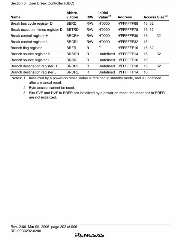
Section 6 User Break Controller (UBC)
Rev. 2.00 Mar 09, 2006 page 202 of 906REJ09B0292-0200
NameAbbre-viation R/W
InitialValue*1 Address Access Size*2
Break bus cycle register D BBRD R/W H'0000 H'FFFFFF68 16, 32
Break execution times register D BETRD R/W H'0000 H'FFFFFF78 16, 32
Break control register H BRCRH R/W H'0000 H'FFFFFF30 16 32
Break control register L BRCRL R/W H'0000 H'FFFFFF32 16
Branch flag register BRFR R *3 H'FFFFFF10 16, 32
Branch source register H BRSRH R Undefined H'FFFFFF14 16 32
Branch source register L BRSRL R Undefined H'FFFFFF16 16
Branch destination register H BRDRH R Undefined H'FFFFFF18 16 32
Branch destination register L BRDRL R Undefined H'FFFFFF1A 16 Notes: 1. Initialized by a power-on reset. Value is retained in standby mode, and is undefined
after a manual reset.2. Byte access cannot be used.3. Bits SVF and DVF in BRFR are initialized by a power-on reset; the other bits in BRFR
are not initialized.
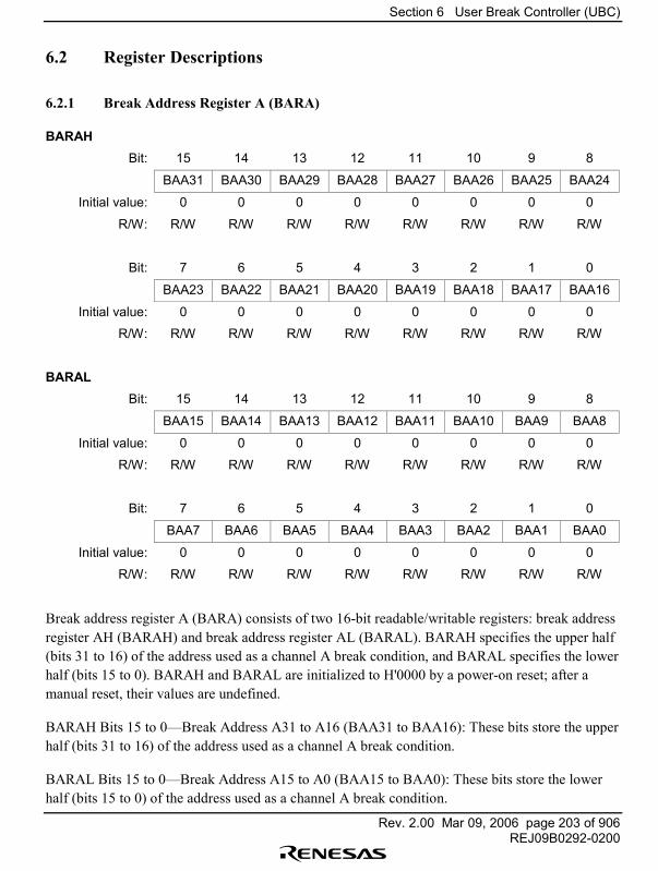
Section 6 User Break Controller (UBC)
Rev. 2.00 Mar 09, 2006 page 203 of 906REJ09B0292-0200
6.2 Register Descriptions
6.2.1 Break Address Register A (BARA)
BARAHBit: 15 14 13 12 11 10 9 8
BAA31 BAA30 BAA29 BAA28 BAA27 BAA26 BAA25 BAA24
Initial value: 0 0 0 0 0 0 0 0
R/W: R/W R/W R/W R/W R/W R/W R/W R/W
Bit: 7 6 5 4 3 2 1 0
BAA23 BAA22 BAA21 BAA20 BAA19 BAA18 BAA17 BAA16
Initial value: 0 0 0 0 0 0 0 0
R/W: R/W R/W R/W R/W R/W R/W R/W R/W
BARALBit: 15 14 13 12 11 10 9 8
BAA15 BAA14 BAA13 BAA12 BAA11 BAA10 BAA9 BAA8
Initial value: 0 0 0 0 0 0 0 0
R/W: R/W R/W R/W R/W R/W R/W R/W R/W
Bit: 7 6 5 4 3 2 1 0
BAA7 BAA6 BAA5 BAA4 BAA3 BAA2 BAA1 BAA0
Initial value: 0 0 0 0 0 0 0 0
R/W: R/W R/W R/W R/W R/W R/W R/W R/W
Break address register A (BARA) consists of two 16-bit readable/writable registers: break addressregister AH (BARAH) and break address register AL (BARAL). BARAH specifies the upper half(bits 31 to 16) of the address used as a channel A break condition, and BARAL specifies the lowerhalf (bits 15 to 0). BARAH and BARAL are initialized to H'0000 by a power-on reset; after amanual reset, their values are undefined.
BARAH Bits 15 to 0�Break Address A31 to A16 (BAA31 to BAA16): These bits store the upperhalf (bits 31 to 16) of the address used as a channel A break condition.
BARAL Bits 15 to 0�Break Address A15 to A0 (BAA15 to BAA0): These bits store the lowerhalf (bits 15 to 0) of the address used as a channel A break condition.
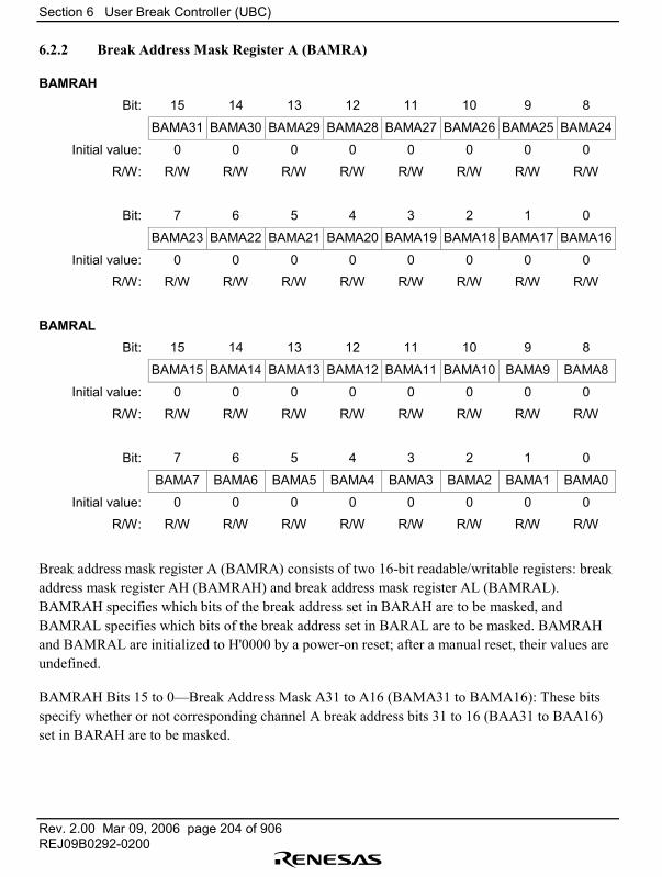
Section 6 User Break Controller (UBC)
Rev. 2.00 Mar 09, 2006 page 204 of 906REJ09B0292-0200
6.2.2 Break Address Mask Register A (BAMRA)
BAMRAHBit: 15 14 13 12 11 10 9 8
BAMA31 BAMA30 BAMA29 BAMA28 BAMA27 BAMA26 BAMA25 BAMA24
Initial value: 0 0 0 0 0 0 0 0
R/W: R/W R/W R/W R/W R/W R/W R/W R/W
Bit: 7 6 5 4 3 2 1 0
BAMA23 BAMA22 BAMA21 BAMA20 BAMA19 BAMA18 BAMA17 BAMA16
Initial value: 0 0 0 0 0 0 0 0
R/W: R/W R/W R/W R/W R/W R/W R/W R/W
BAMRALBit: 15 14 13 12 11 10 9 8
BAMA15 BAMA14 BAMA13 BAMA12 BAMA11 BAMA10 BAMA9 BAMA8
Initial value: 0 0 0 0 0 0 0 0
R/W: R/W R/W R/W R/W R/W R/W R/W R/W
Bit: 7 6 5 4 3 2 1 0
BAMA7 BAMA6 BAMA5 BAMA4 BAMA3 BAMA2 BAMA1 BAMA0
Initial value: 0 0 0 0 0 0 0 0
R/W: R/W R/W R/W R/W R/W R/W R/W R/W
Break address mask register A (BAMRA) consists of two 16-bit readable/writable registers: breakaddress mask register AH (BAMRAH) and break address mask register AL (BAMRAL).BAMRAH specifies which bits of the break address set in BARAH are to be masked, andBAMRAL specifies which bits of the break address set in BARAL are to be masked. BAMRAHand BAMRAL are initialized to H'0000 by a power-on reset; after a manual reset, their values areundefined.
BAMRAH Bits 15 to 0�Break Address Mask A31 to A16 (BAMA31 to BAMA16): These bitsspecify whether or not corresponding channel A break address bits 31 to 16 (BAA31 to BAA16)set in BARAH are to be masked.
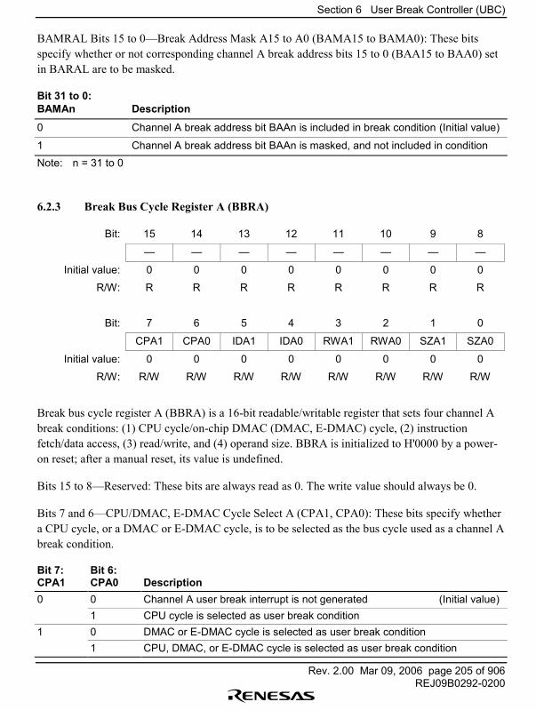
Section 6 User Break Controller (UBC)
Rev. 2.00 Mar 09, 2006 page 205 of 906REJ09B0292-0200
BAMRAL Bits 15 to 0�Break Address Mask A15 to A0 (BAMA15 to BAMA0): These bitsspecify whether or not corresponding channel A break address bits 15 to 0 (BAA15 to BAA0) setin BARAL are to be masked.
Bit 31 to 0:BAMAn Description
0 Channel A break address bit BAAn is included in break condition (Initial value)
1 Channel A break address bit BAAn is masked, and not included in conditionNote: n = 31 to 0
6.2.3 Break Bus Cycle Register A (BBRA)
Bit: 15 14 13 12 11 10 9 8
� � � � � � � �
Initial value: 0 0 0 0 0 0 0 0
R/W: R R R R R R R R
Bit: 7 6 5 4 3 2 1 0
CPA1 CPA0 IDA1 IDA0 RWA1 RWA0 SZA1 SZA0
Initial value: 0 0 0 0 0 0 0 0
R/W: R/W R/W R/W R/W R/W R/W R/W R/W
Break bus cycle register A (BBRA) is a 16-bit readable/writable register that sets four channel Abreak conditions: (1) CPU cycle/on-chip DMAC (DMAC, E-DMAC) cycle, (2) instructionfetch/data access, (3) read/write, and (4) operand size. BBRA is initialized to H'0000 by a power-on reset; after a manual reset, its value is undefined.
Bits 15 to 8�Reserved: These bits are always read as 0. The write value should always be 0.
Bits 7 and 6�CPU/DMAC, E-DMAC Cycle Select A (CPA1, CPA0): These bits specify whethera CPU cycle, or a DMAC or E-DMAC cycle, is to be selected as the bus cycle used as a channel Abreak condition.
Bit 7:CPA1
Bit 6:CPA0 Description
0 0 Channel A user break interrupt is not generated (Initial value)1 CPU cycle is selected as user break condition
1 0 DMAC or E-DMAC cycle is selected as user break condition1 CPU, DMAC, or E-DMAC cycle is selected as user break condition
Section 6 User Break Controller (UBC)
Rev. 2.00 Mar 09, 2006 page 206 of 906REJ09B0292-0200
Bits 5 and 4�Instruction Fetch/Data Access Select A (IDA1, IDA0): These bits specify whetheran instruction fetch cycle or data access cycle is to be selected as the bus cycle used as a channel Abreak condition.
Bit 5:IDA1
Bit 4:IDA0 Description
0 0 Channel A user break interrupt is not generated (Initial value)
1 Instruction fetch cycle is selected as break condition
1 0 Data access cycle is selected as break condition
1 Instruction fetch cycle or data access cycle is selected as break condition
Bits 3 and 2�Read/Write Select A (RWA1, RWA0): These bits specify whether a read cycle orwrite cycle is to be selected as the bus cycle used as a channel A break condition.
Bit 3:RWA1
Bit 2:RWA0 Description
0 0 Channel A user break interrupt is not generated (Initial value)
1 Read cycle is selected as break condition
1 0 Write cycle is selected as break condition
1 Read cycle or write cycle is selected as break condition
Bits 1 and 0�Operand Size Select A (SZA1, SZA0): These bits select the operand size of the buscycle used as a channel A break condition.
Bit 1:SZA1
Bit 0:SZA0 Description
0 0 Operand size is not included in break conditions (Initial value)
1 Byte access is selected as break condition
1 0 Word access is selected as break condition
1 Longword access is selected as break conditionNotes: When a break is to be executed on an instruction fetch, clear the SZA0 bit to 0. All
instructions are regarded as being accessed using word size (instruction fetches are alwaysperformed as longword).In the case of an instruction, the operand size is word; in the case of a CPU/DMAC, E-DMAC data access, it is determined by the specified operand size. Note that the operandsize is not determined by the bus width of the space accessed.
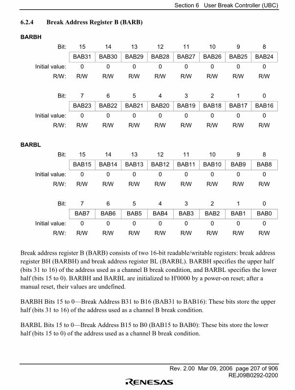
Section 6 User Break Controller (UBC)
Rev. 2.00 Mar 09, 2006 page 207 of 906REJ09B0292-0200
6.2.4 Break Address Register B (BARB)
BARBHBit: 15 14 13 12 11 10 9 8
BAB31 BAB30 BAB29 BAB28 BAB27 BAB26 BAB25 BAB24
Initial value: 0 0 0 0 0 0 0 0
R/W: R/W R/W R/W R/W R/W R/W R/W R/W
Bit: 7 6 5 4 3 2 1 0
BAB23 BAB22 BAB21 BAB20 BAB19 BAB18 BAB17 BAB16
Initial value: 0 0 0 0 0 0 0 0
R/W: R/W R/W R/W R/W R/W R/W R/W R/W
BARBLBit: 15 14 13 12 11 10 9 8
BAB15 BAB14 BAB13 BAB12 BAB11 BAB10 BAB9 BAB8
Initial value: 0 0 0 0 0 0 0 0
R/W: R/W R/W R/W R/W R/W R/W R/W R/W
Bit: 7 6 5 4 3 2 1 0
BAB7 BAB6 BAB5 BAB4 BAB3 BAB2 BAB1 BAB0
Initial value: 0 0 0 0 0 0 0 0
R/W: R/W R/W R/W R/W R/W R/W R/W R/W
Break address register B (BARB) consists of two 16-bit readable/writable registers: break addressregister BH (BARBH) and break address register BL (BARBL). BARBH specifies the upper half(bits 31 to 16) of the address used as a channel B break condition, and BARBL specifies the lowerhalf (bits 15 to 0). BARBH and BARBL are initialized to H'0000 by a power-on reset; after amanual reset, their values are undefined.
BARBH Bits 15 to 0�Break Address B31 to B16 (BAB31 to BAB16): These bits store the upperhalf (bits 31 to 16) of the address used as a channel B break condition.
BARBL Bits 15 to 0�Break Address B15 to B0 (BAB15 to BAB0): These bits store the lowerhalf (bits 15 to 0) of the address used as a channel B break condition.
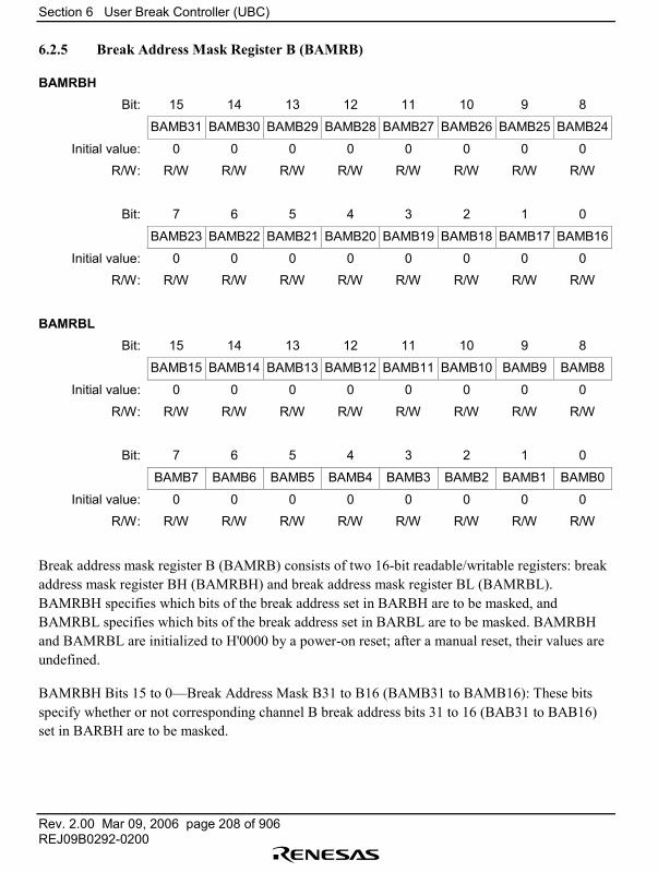
Section 6 User Break Controller (UBC)
Rev. 2.00 Mar 09, 2006 page 208 of 906REJ09B0292-0200
6.2.5 Break Address Mask Register B (BAMRB)
BAMRBHBit: 15 14 13 12 11 10 9 8
BAMB31 BAMB30 BAMB29 BAMB28 BAMB27 BAMB26 BAMB25 BAMB24
Initial value: 0 0 0 0 0 0 0 0
R/W: R/W R/W R/W R/W R/W R/W R/W R/W
Bit: 7 6 5 4 3 2 1 0
BAMB23 BAMB22 BAMB21 BAMB20 BAMB19 BAMB18 BAMB17 BAMB16
Initial value: 0 0 0 0 0 0 0 0
R/W: R/W R/W R/W R/W R/W R/W R/W R/W
BAMRBLBit: 15 14 13 12 11 10 9 8
BAMB15 BAMB14 BAMB13 BAMB12 BAMB11 BAMB10 BAMB9 BAMB8
Initial value: 0 0 0 0 0 0 0 0
R/W: R/W R/W R/W R/W R/W R/W R/W R/W
Bit: 7 6 5 4 3 2 1 0
BAMB7 BAMB6 BAMB5 BAMB4 BAMB3 BAMB2 BAMB1 BAMB0
Initial value: 0 0 0 0 0 0 0 0
R/W: R/W R/W R/W R/W R/W R/W R/W R/W
Break address mask register B (BAMRB) consists of two 16-bit readable/writable registers: breakaddress mask register BH (BAMRBH) and break address mask register BL (BAMRBL).BAMRBH specifies which bits of the break address set in BARBH are to be masked, andBAMRBL specifies which bits of the break address set in BARBL are to be masked. BAMRBHand BAMRBL are initialized to H'0000 by a power-on reset; after a manual reset, their values areundefined.
BAMRBH Bits 15 to 0�Break Address Mask B31 to B16 (BAMB31 to BAMB16): These bitsspecify whether or not corresponding channel B break address bits 31 to 16 (BAB31 to BAB16)set in BARBH are to be masked.
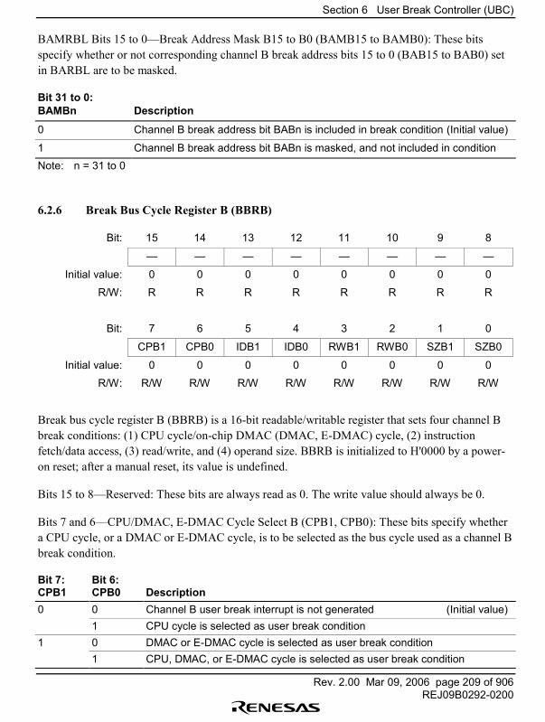
Section 6 User Break Controller (UBC)
Rev. 2.00 Mar 09, 2006 page 209 of 906REJ09B0292-0200
BAMRBL Bits 15 to 0�Break Address Mask B15 to B0 (BAMB15 to BAMB0): These bitsspecify whether or not corresponding channel B break address bits 15 to 0 (BAB15 to BAB0) setin BARBL are to be masked.
Bit 31 to 0:BAMBn Description
0 Channel B break address bit BABn is included in break condition (Initial value)
1 Channel B break address bit BABn is masked, and not included in conditionNote: n = 31 to 0
6.2.6 Break Bus Cycle Register B (BBRB)
Bit: 15 14 13 12 11 10 9 8
� � � � � � � �
Initial value: 0 0 0 0 0 0 0 0
R/W: R R R R R R R R
Bit: 7 6 5 4 3 2 1 0
CPB1 CPB0 IDB1 IDB0 RWB1 RWB0 SZB1 SZB0
Initial value: 0 0 0 0 0 0 0 0
R/W: R/W R/W R/W R/W R/W R/W R/W R/W
Break bus cycle register B (BBRB) is a 16-bit readable/writable register that sets four channel Bbreak conditions: (1) CPU cycle/on-chip DMAC (DMAC, E-DMAC) cycle, (2) instructionfetch/data access, (3) read/write, and (4) operand size. BBRB is initialized to H'0000 by a power-on reset; after a manual reset, its value is undefined.
Bits 15 to 8�Reserved: These bits are always read as 0. The write value should always be 0.
Bits 7 and 6�CPU/DMAC, E-DMAC Cycle Select B (CPB1, CPB0): These bits specify whethera CPU cycle, or a DMAC or E-DMAC cycle, is to be selected as the bus cycle used as a channel Bbreak condition.
Bit 7:CPB1
Bit 6:CPB0 Description
0 0 Channel B user break interrupt is not generated (Initial value)1 CPU cycle is selected as user break condition
1 0 DMAC or E-DMAC cycle is selected as user break condition1 CPU, DMAC, or E-DMAC cycle is selected as user break condition

Section 6 User Break Controller (UBC)
Rev. 2.00 Mar 09, 2006 page 210 of 906REJ09B0292-0200
Bits 5 and 4�Instruction Fetch/Data Access Select B (IDB1, IDB0): These bits specify whetheran instruction fetch cycle or data access cycle is to be selected as the bus cycle used as a channel Bbreak condition.
Bit 5:IDB1
Bit 4:IDB0 Description
0 0 Channel B user break interrupt is not generated (Initial value)
1 Instruction fetch cycle is selected as break condition
1 0 Data access cycle is selected as break condition
1 Instruction fetch cycle or data access cycle is selected as break condition
Bits 3 and 2�Read/Write Select B (RWB1, RWB0): These bits specify whether a read cycle orwrite cycle is to be selected as the bus cycle used as a channel B break condition.
Bit 3:RWB1
Bit 2:RWB0 Description
0 0 Channel B user break interrupt is not generated (Initial value)
1 Read cycle is selected as break condition
1 0 Write cycle is selected as break condition
1 Read cycle or write cycle is selected as break condition
Bits 1 and 0�Operand Size Select B (SZB1, SZB0): These bits select the operand size of the buscycle used as a channel B break condition.
Bit 1:SZB1
Bit 0:SZB0 Description
0 0 Operand size is not included in break conditions (Initial value)
1 Byte access is selected as break condition
1 0 Word access is selected as break condition
1 Longword access is selected as break conditionNotes: When a break is to be executed on an instruction fetch, clear the SZB0 bit to 0. All
instructions are regarded as being accessed using word size (instruction fetches are alwaysperformed as longword).In the case of an instruction, the operand size is word; in the case of a CPU/DMAC, E-DMAC data access, it is determined by the specified operand size. Note that the operandsize is not determined by the bus width of the space accessed.
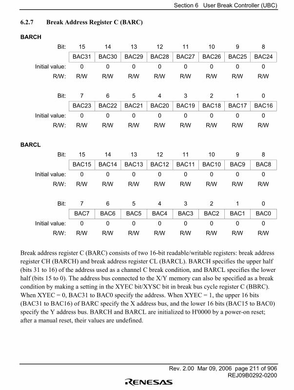
Section 6 User Break Controller (UBC)
Rev. 2.00 Mar 09, 2006 page 211 of 906REJ09B0292-0200
6.2.7 Break Address Register C (BARC)
BARCHBit: 15 14 13 12 11 10 9 8
BAC31 BAC30 BAC29 BAC28 BAC27 BAC26 BAC25 BAC24
Initial value: 0 0 0 0 0 0 0 0
R/W: R/W R/W R/W R/W R/W R/W R/W R/W
Bit: 7 6 5 4 3 2 1 0
BAC23 BAC22 BAC21 BAC20 BAC19 BAC18 BAC17 BAC16
Initial value: 0 0 0 0 0 0 0 0
R/W: R/W R/W R/W R/W R/W R/W R/W R/W
BARCLBit: 15 14 13 12 11 10 9 8
BAC15 BAC14 BAC13 BAC12 BAC11 BAC10 BAC9 BAC8
Initial value: 0 0 0 0 0 0 0 0
R/W: R/W R/W R/W R/W R/W R/W R/W R/W
Bit: 7 6 5 4 3 2 1 0
BAC7 BAC6 BAC5 BAC4 BAC3 BAC2 BAC1 BAC0
Initial value: 0 0 0 0 0 0 0 0
R/W: R/W R/W R/W R/W R/W R/W R/W R/W
Break address register C (BARC) consists of two 16-bit readable/writable registers: break addressregister CH (BARCH) and break address register CL (BARCL). BARCH specifies the upper half(bits 31 to 16) of the address used as a channel C break condition, and BARCL specifies the lowerhalf (bits 15 to 0). The address bus connected to the X/Y memory can also be specified as a breakcondition by making a setting in the XYEC bit/XYSC bit in break bus cycle register C (BBRC).When XYEC = 0, BAC31 to BAC0 specify the address. When XYEC = 1, the upper 16 bits(BAC31 to BAC16) of BARC specify the X address bus, and the lower 16 bits (BAC15 to BAC0)specify the Y address bus. BARCH and BARCL are initialized to H'0000 by a power-on reset;after a manual reset, their values are undefined.

Section 6 User Break Controller (UBC)
Rev. 2.00 Mar 09, 2006 page 212 of 906REJ09B0292-0200
BARC Configuration
Upper 16 Bits(BAC31 to BAC16)
Lower 16 Bits(BAC15 to BAC0)
XYEC = 0 Address Upper 16 bits of address bus Lower 16 bits of address bus
XYEC = 1 X address(when XYSC = 0)
X address(XAB15 to XAB1)*
�
Y address(when XYSC = 1)
� Y address(YAB15 to YAB1)*
Note: * As an X/Y bus access is always a word access, the values of XAB0 and YAB0 is notincluded in the break condition.
6.2.8 Break Address Mask Register C (BAMRC)
BAMRCHBit: 15 14 13 12 11 10 9 8
BAMC31 BAMC30 BAMC29 BAMC28 BAMC27 BAMC26 BAMC25 BAMC24
Initial value: 0 0 0 0 0 0 0 0
R/W: R/W R/W R/W R/W R/W R/W R/W R/W
Bit: 7 6 5 4 3 2 1 0
BAMC23 BAMC22 BAMC21 BAMC20 BAMC19 BAMC18 BAMC17 BAMC16
Initial value: 0 0 0 0 0 0 0 0
R/W: R/W R/W R/W R/W R/W R/W R/W R/W
BAMRCLBit: 15 14 13 12 11 10 9 8
BAMC15 BAMC14 BAMC13 BAMC12 BAMC11 BAMC10 BAMC9 BAMC8
Initial value: 0 0 0 0 0 0 0 0
R/W: R/W R/W R/W R/W R/W R/W R/W R/W
Bit: 7 6 5 4 3 2 1 0
BAMC7 BAMC6 BAMC5 BAMC4 BAMC3 BAMC2 BAMC1 BAMC0
Initial value: 0 0 0 0 0 0 0 0
R/W: R/W R/W R/W R/W R/W R/W R/W R/W

Section 6 User Break Controller (UBC)
Rev. 2.00 Mar 09, 2006 page 213 of 906REJ09B0292-0200
Break address mask register C (BAMRC) consists of two 16-bit readable/writable registers: breakaddress mask register CH (BAMRCH) and break address mask register CL (BAMRCL).BAMRCH specifies which bits of the break address set in BARCH are to be masked, andBAMRCL specifies which bits of the break address set in BARCL are to be masked. Operationalso depends on bits XYEC and XYSC in BBRC as shown below.
BAMRC Configuration
Upper 16 Bits(BAMC31 to BAMC16)
Lower 16 Bits(BAMC15 to BAMC0)
XYEC = 0 Address Upper 16 bits maskable Lower 16 bits maskable
XYEC = 1 X address(when XYSC = 0)
Maskable �
Y address(when XYSC = 1
� Maskable
Bit 31 to 0:BAMCn Description
0 Channel C break address bit BACn is included in break condition (Initial value)
1 Channel C break address bit BACn is masked, and not included in conditionNote: n = 31 to 0
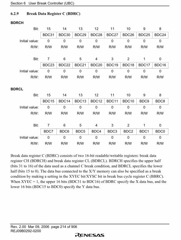
Section 6 User Break Controller (UBC)
Rev. 2.00 Mar 09, 2006 page 214 of 906REJ09B0292-0200
6.2.9 Break Data Register C (BDRC)
BDRCHBit: 15 14 13 12 11 10 9 8
BDC31 BDC30 BDC29 BDC28 BDC27 BDC26 BDC25 BDC24
Initial value: 0 0 0 0 0 0 0 0
R/W: R/W R/W R/W R/W R/W R/W R/W R/W
Bit: 7 6 5 4 3 2 1 0
BDC23 BDC22 BDC21 BDC20 BDC19 BDC18 BDC17 BDC16
Initial value: 0 0 0 0 0 0 0 0
R/W: R/W R/W R/W R/W R/W R/W R/W R/W
BDRCLBit: 15 14 13 12 11 10 9 8
BDC15 BDC14 BDC13 BDC12 BDC11 BDC10 BDC9 BDC8
Initial value: 0 0 0 0 0 0 0 0
R/W: R/W R/W R/W R/W R/W R/W R/W R/W
Bit: 7 6 5 4 3 2 1 0
BDC7 BDC6 BDC5 BDC4 BDC3 BDC2 BDC1 BDC0
Initial value: 0 0 0 0 0 0 0 0
R/W: R/W R/W R/W R/W R/W R/W R/W R/W
Break data register C (BDRC) consists of two 16-bit readable/writable registers: break dataregister CH (BDRCH) and break data register CL (BDRCL). BDRCH specifies the upper half(bits 31 to 16) of the data used as a channel C break condition, and BDRCL specifies the lowerhalf (bits 15 to 0). The data bus connected to the X/Y memory can also be specified as a breakcondition by making a setting in the XYEC bit/XYSC bit in break bus cycle register C (BBRC).When XYEC = 1, the upper 16 bits (BDC31 to BDC16) of BDRC specify the X data bus, and thelower 16 bits (BDC15 to BDC0) specify the Y data bus.
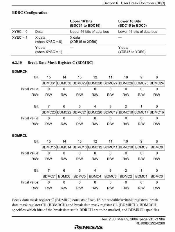
Section 6 User Break Controller (UBC)
Rev. 2.00 Mar 09, 2006 page 215 of 906REJ09B0292-0200
BDRC Configuration
Upper 16 Bits(BDC31 to BDC16)
Lower 16 Bits(BDC15 to BDC0)
XYEC = 0 Data Upper 16 bits of data bus Lower 16 bits of data bus
XYEC = 1 X data(when XYSC = 0)
X data(XDB15 to XDB0)
�
Y data(when XYSC = 1)
� Y data(YDB15 to YDB0)
6.2.10 Break Data Mask Register C (BDMRC)
BDMRCHBit: 15 14 13 12 11 10 9 8
BDMC31 BDMC30 BDMC29 BDMC28 BDMC27 BDMC26 BDMC25 BDMC24
Initial value: 0 0 0 0 0 0 0 0
R/W: R/W R/W R/W R/W R/W R/W R/W R/W
Bit: 7 6 5 4 3 2 1 0
BDMC23 BDMC22 BDMC21 BDMC20 BDMC19 BDMC18 BDMC17 BDMC16
Initial value: 0 0 0 0 0 0 0 0
R/W: R/W R/W R/W R/W R/W R/W R/W R/W
BDMRCLBit: 15 14 13 12 11 10 9 8
BDMC15 BDMC14 BDMC13 BDMC12 BDMC11 BDMC10 BDMC9 BDMC8
Initial value: 0 0 0 0 0 0 0 0
R/W: R/W R/W R/W R/W R/W R/W R/W R/W
Bit: 7 6 5 4 3 2 1 0
BDMC7 BDMC6 BDMC5 BDMC4 BDMC3 BDMC2 BDMC1 BDMC0
Initial value: 0 0 0 0 0 0 0 0
R/W: R/W R/W R/W R/W R/W R/W R/W R/W
Break data mask register C (BDMRC) consists of two 16-bit readable/writable registers: breakdata mask register CH (BDMRCH) and break data mask register CL (BDMRCL). BDMRCHspecifies which bits of the break data set in BDRCH are to be masked, and BDMRCL specifies
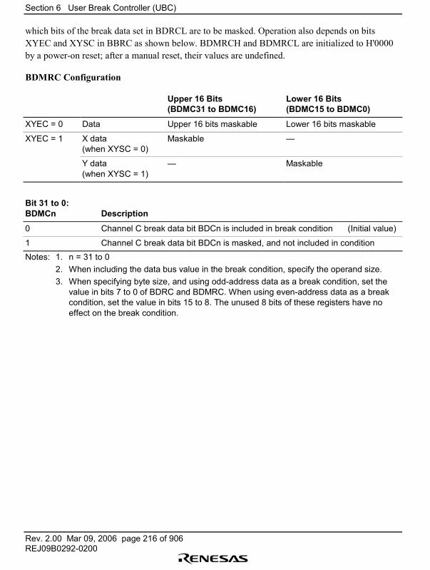
Section 6 User Break Controller (UBC)
Rev. 2.00 Mar 09, 2006 page 216 of 906REJ09B0292-0200
which bits of the break data set in BDRCL are to be masked. Operation also depends on bitsXYEC and XYSC in BBRC as shown below. BDMRCH and BDMRCL are initialized to H'0000by a power-on reset; after a manual reset, their values are undefined.
BDMRC Configuration
Upper 16 Bits(BDMC31 to BDMC16)
Lower 16 Bits(BDMC15 to BDMC0)
XYEC = 0 Data Upper 16 bits maskable Lower 16 bits maskable
XYEC = 1 X data(when XYSC = 0)
Maskable �
Y data(when XYSC = 1)
� Maskable
Bit 31 to 0:BDMCn Description
0 Channel C break data bit BDCn is included in break condition (Initial value)
1 Channel C break data bit BDCn is masked, and not included in conditionNotes: 1. n = 31 to 0
2. When including the data bus value in the break condition, specify the operand size.3. When specifying byte size, and using odd-address data as a break condition, set the
value in bits 7 to 0 of BDRC and BDMRC. When using even-address data as a breakcondition, set the value in bits 15 to 8. The unused 8 bits of these registers have noeffect on the break condition.
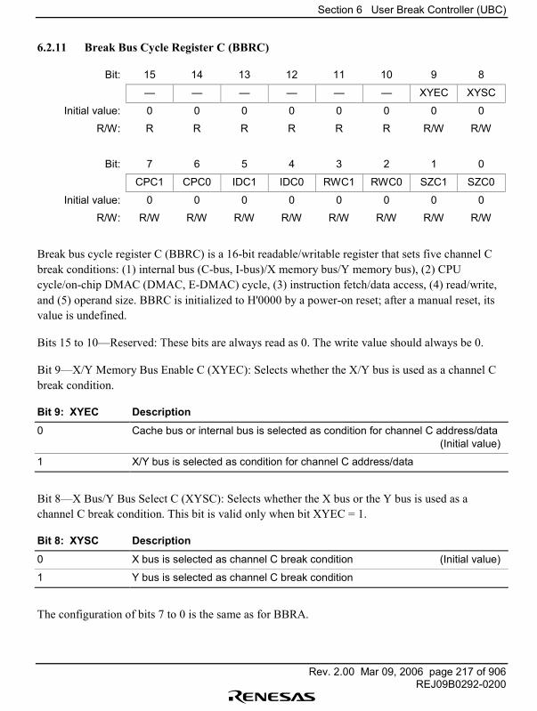
Section 6 User Break Controller (UBC)
Rev. 2.00 Mar 09, 2006 page 217 of 906REJ09B0292-0200
6.2.11 Break Bus Cycle Register C (BBRC)
Bit: 15 14 13 12 11 10 9 8
� � � � � � XYEC XYSC
Initial value: 0 0 0 0 0 0 0 0
R/W: R R R R R R R/W R/W
Bit: 7 6 5 4 3 2 1 0
CPC1 CPC0 IDC1 IDC0 RWC1 RWC0 SZC1 SZC0
Initial value: 0 0 0 0 0 0 0 0
R/W: R/W R/W R/W R/W R/W R/W R/W R/W
Break bus cycle register C (BBRC) is a 16-bit readable/writable register that sets five channel Cbreak conditions: (1) internal bus (C-bus, I-bus)/X memory bus/Y memory bus), (2) CPUcycle/on-chip DMAC (DMAC, E-DMAC) cycle, (3) instruction fetch/data access, (4) read/write,and (5) operand size. BBRC is initialized to H'0000 by a power-on reset; after a manual reset, itsvalue is undefined.
Bits 15 to 10�Reserved: These bits are always read as 0. The write value should always be 0.
Bit 9�X/Y Memory Bus Enable C (XYEC): Selects whether the X/Y bus is used as a channel Cbreak condition.
Bit 9: XYEC Description
0 Cache bus or internal bus is selected as condition for channel C address/data(Initial value)
1 X/Y bus is selected as condition for channel C address/data
Bit 8�X Bus/Y Bus Select C (XYSC): Selects whether the X bus or the Y bus is used as achannel C break condition. This bit is valid only when bit XYEC = 1.
Bit 8: XYSC Description
0 X bus is selected as channel C break condition (Initial value)
1 Y bus is selected as channel C break condition
The configuration of bits 7 to 0 is the same as for BBRA.

Section 6 User Break Controller (UBC)
Rev. 2.00 Mar 09, 2006 page 218 of 906REJ09B0292-0200
6.2.12 Break Execution Times Register C (BETRC)
Bit: 15 14 13 12 11 10 9 8
� � � � ETRC11 ETRC10 ETRC9 ETRC8
Initial value: 0 0 0 0 0 0 0 0
R/W: R R R R R/W R/W R/W R/W
Bit: 7 6 5 4 3 2 1 0
ETRC7 ETRC6 ETRC5 ETRC4 ETRC3 ETRC2 ETRC1 ETRC0
Initial value: 0 0 0 0 0 0 0 0
R/W: R/W R/W R/W R/W R/W R/W R/W R/W
When a channel C execution-times break condition is enabled (by setting the ETBEC bit inBRCR), this 16-bit register specifies the number of times a channel C break condition occursbefore a user break interrupt is requested. The maximum value is 212 � 1 times. Each time achannel C break condition occurs, the value in BETRC is decremented by 1. After the BETRCvalue reaches H'0001, an interrupt is requested when a break condition next occurs.
As exceptions and interrupts cannot be accepted for instructions in a repeat loop comprising nomore than three instructions, BETRC is not decremented by the occurrence of a break conditionfor an instruction in such a repeat loop (see 4.6, When Exception Sources Are Not Accepted).
Bits 15 to 12 are always read as 0, and should only be written with 0.
BETRC is initialized to H'0000 by a power-on reset.

Section 6 User Break Controller (UBC)
Rev. 2.00 Mar 09, 2006 page 219 of 906REJ09B0292-0200
6.2.13 Break Address Register D (BARD)
BARDHBit 15 14 13 12 11 10 9 8
BAD31 BAD30 BAD29 BAD28 BAD27 BAD26 BAD25 BAD24
Initial value 0 0 0 0 0 0 0 0
Read/Write R/W R/W R/W R/W R/W R/W R/W R/W
Bit 7 6 5 4 3 2 1 0
BAD23 BAD22 BAD21 BAD20 BAD19 BAD18 BAD17 BAD16
Initial value 0 0 0 0 0 0 0 0
Read/Write R/W R/W R/W R/W R/W R/W R/W R/W
BARDLBit 15 14 13 12 11 10 9 8
BAD15 BAD14 BAD13 BAD12 BAD11 BAD10 BAD9 BAD8
Initial value 0 0 0 0 0 0 0 0
Read/Write R/W R/W R/W R/W R/W R/W R/W R/W
Bit 7 6 5 4 3 2 1 0
BAD7 BAD6 BAD5 BAD4 BAD3 BAD2 BAD1 BAD0
Initial value 0 0 0 0 0 0 0 0
Read/Write R/W R/W R/W R/W R/W R/W R/W R/W
Break address register D (BARD) consists of two 16-bit readable/writable registers: break addressregister DH (BARDH) and break address register DL (BARDL). BARDH specifies the upper half(bits 31 to 16) of the address used as a channel D break condition, and BARDL specifies the lowerhalf (bits 15 to 0). The address bus connected to the X/Y memory can also be specified as a breakcondition by making a setting in the XYED bit/XYSD bit in break bus cycle register D (BBRD).When XYED = 0, BAD31 to BAD0 specify the address. When XYED = 1, the upper 16 bits(BAD31 to BAD16) of BARD specify the X address bus, and the lower 16 bits (BAD15 to BAD0)specify the Y address bus. BARDH and BARDL are initialized to H'0000 by a power-on reset;after a manual reset, their values are undefined.
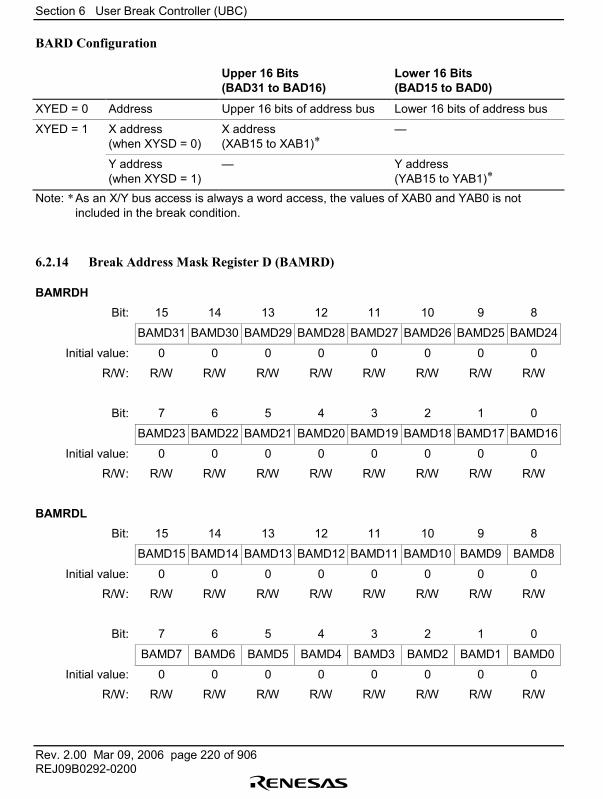
Section 6 User Break Controller (UBC)
Rev. 2.00 Mar 09, 2006 page 220 of 906REJ09B0292-0200
BARD Configuration
Upper 16 Bits(BAD31 to BAD16)
Lower 16 Bits(BAD15 to BAD0)
XYED = 0 Address Upper 16 bits of address bus Lower 16 bits of address bus
XYED = 1 X address(when XYSD = 0)
X address(XAB15 to XAB1)*
�
Y address(when XYSD = 1)
� Y address(YAB15 to YAB1)*
Note: * As an X/Y bus access is always a word access, the values of XAB0 and YAB0 is notincluded in the break condition.
6.2.14 Break Address Mask Register D (BAMRD)
BAMRDHBit: 15 14 13 12 11 10 9 8
BAMD31 BAMD30 BAMD29 BAMD28 BAMD27 BAMD26 BAMD25 BAMD24
Initial value: 0 0 0 0 0 0 0 0
R/W: R/W R/W R/W R/W R/W R/W R/W R/W
Bit: 7 6 5 4 3 2 1 0
BAMD23 BAMD22 BAMD21 BAMD20 BAMD19 BAMD18 BAMD17 BAMD16
Initial value: 0 0 0 0 0 0 0 0
R/W: R/W R/W R/W R/W R/W R/W R/W R/W
BAMRDLBit: 15 14 13 12 11 10 9 8
BAMD15 BAMD14 BAMD13 BAMD12 BAMD11 BAMD10 BAMD9 BAMD8
Initial value: 0 0 0 0 0 0 0 0
R/W: R/W R/W R/W R/W R/W R/W R/W R/W
Bit: 7 6 5 4 3 2 1 0
BAMD7 BAMD6 BAMD5 BAMD4 BAMD3 BAMD2 BAMD1 BAMD0
Initial value: 0 0 0 0 0 0 0 0
R/W: R/W R/W R/W R/W R/W R/W R/W R/W
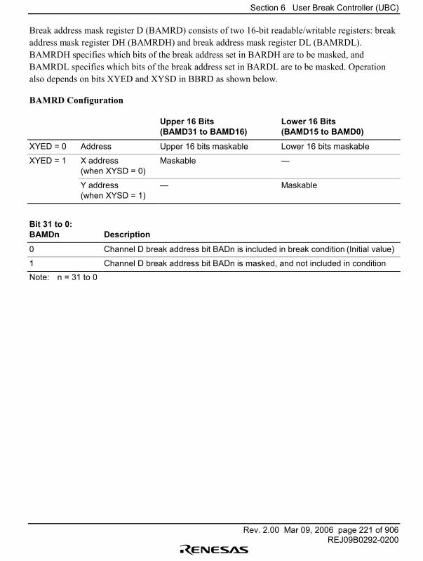
Section 6 User Break Controller (UBC)
Rev. 2.00 Mar 09, 2006 page 221 of 906REJ09B0292-0200
Break address mask register D (BAMRD) consists of two 16-bit readable/writable registers: breakaddress mask register DH (BAMRDH) and break address mask register DL (BAMRDL).BAMRDH specifies which bits of the break address set in BARDH are to be masked, andBAMRDL specifies which bits of the break address set in BARDL are to be masked. Operationalso depends on bits XYED and XYSD in BBRD as shown below.
BAMRD Configuration
Upper 16 Bits(BAMD31 to BAMD16)
Lower 16 Bits(BAMD15 to BAMD0)
XYED = 0 Address Upper 16 bits maskable Lower 16 bits maskable
XYED = 1 X address(when XYSD = 0)
Maskable �
Y address(when XYSD = 1)
� Maskable
Bit 31 to 0:BAMDn Description
0 Channel D break address bit BADn is included in break condition (Initial value)
1 Channel D break address bit BADn is masked, and not included in conditionNote: n = 31 to 0
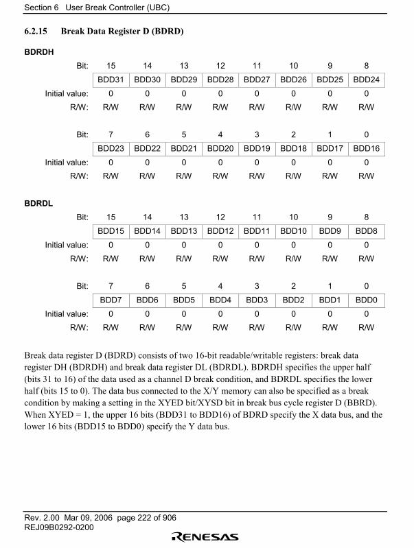
Section 6 User Break Controller (UBC)
Rev. 2.00 Mar 09, 2006 page 222 of 906REJ09B0292-0200
6.2.15 Break Data Register D (BDRD)
BDRDHBit: 15 14 13 12 11 10 9 8
BDD31 BDD30 BDD29 BDD28 BDD27 BDD26 BDD25 BDD24
Initial value: 0 0 0 0 0 0 0 0
R/W: R/W R/W R/W R/W R/W R/W R/W R/W
Bit: 7 6 5 4 3 2 1 0
BDD23 BDD22 BDD21 BDD20 BDD19 BDD18 BDD17 BDD16
Initial value: 0 0 0 0 0 0 0 0
R/W: R/W R/W R/W R/W R/W R/W R/W R/W
BDRDLBit: 15 14 13 12 11 10 9 8
BDD15 BDD14 BDD13 BDD12 BDD11 BDD10 BDD9 BDD8
Initial value: 0 0 0 0 0 0 0 0
R/W: R/W R/W R/W R/W R/W R/W R/W R/W
Bit: 7 6 5 4 3 2 1 0
BDD7 BDD6 BDD5 BDD4 BDD3 BDD2 BDD1 BDD0
Initial value: 0 0 0 0 0 0 0 0
R/W: R/W R/W R/W R/W R/W R/W R/W R/W
Break data register D (BDRD) consists of two 16-bit readable/writable registers: break dataregister DH (BDRDH) and break data register DL (BDRDL). BDRDH specifies the upper half(bits 31 to 16) of the data used as a channel D break condition, and BDRDL specifies the lowerhalf (bits 15 to 0). The data bus connected to the X/Y memory can also be specified as a breakcondition by making a setting in the XYED bit/XYSD bit in break bus cycle register D (BBRD).When XYED = 1, the upper 16 bits (BDD31 to BDD16) of BDRD specify the X data bus, and thelower 16 bits (BDD15 to BDD0) specify the Y data bus.
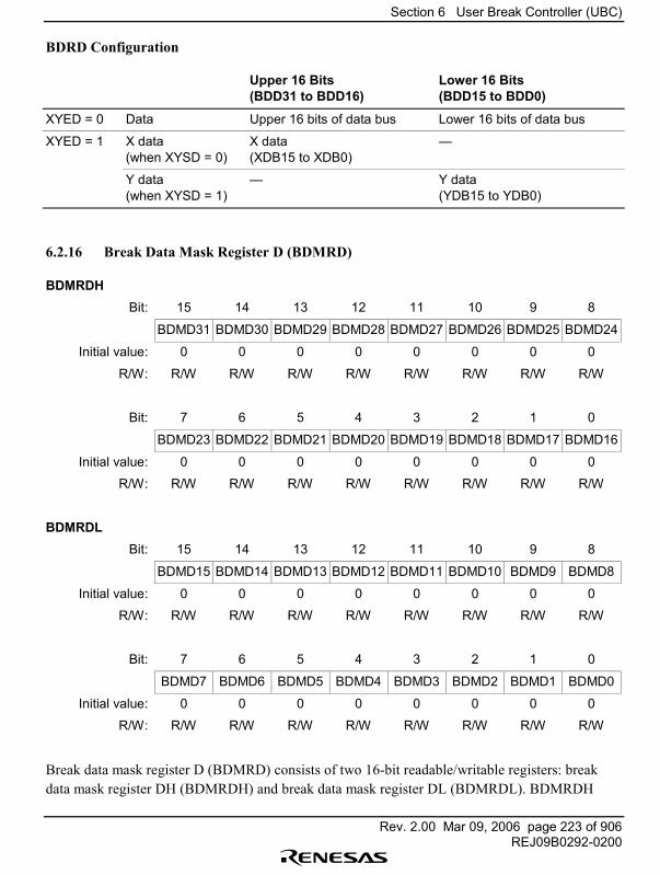
Section 6 User Break Controller (UBC)
Rev. 2.00 Mar 09, 2006 page 223 of 906REJ09B0292-0200
BDRD Configuration
Upper 16 Bits(BDD31 to BDD16)
Lower 16 Bits(BDD15 to BDD0)
XYED = 0 Data Upper 16 bits of data bus Lower 16 bits of data bus
XYED = 1 X data(when XYSD = 0)
X data(XDB15 to XDB0)
�
Y data(when XYSD = 1)
� Y data(YDB15 to YDB0)
6.2.16 Break Data Mask Register D (BDMRD)
BDMRDHBit: 15 14 13 12 11 10 9 8
BDMD31 BDMD30 BDMD29 BDMD28 BDMD27 BDMD26 BDMD25 BDMD24
Initial value: 0 0 0 0 0 0 0 0
R/W: R/W R/W R/W R/W R/W R/W R/W R/W
Bit: 7 6 5 4 3 2 1 0
BDMD23 BDMD22 BDMD21 BDMD20 BDMD19 BDMD18 BDMD17 BDMD16
Initial value: 0 0 0 0 0 0 0 0
R/W: R/W R/W R/W R/W R/W R/W R/W R/W
BDMRDLBit: 15 14 13 12 11 10 9 8
BDMD15 BDMD14 BDMD13 BDMD12 BDMD11 BDMD10 BDMD9 BDMD8
Initial value: 0 0 0 0 0 0 0 0
R/W: R/W R/W R/W R/W R/W R/W R/W R/W
Bit: 7 6 5 4 3 2 1 0
BDMD7 BDMD6 BDMD5 BDMD4 BDMD3 BDMD2 BDMD1 BDMD0
Initial value: 0 0 0 0 0 0 0 0
R/W: R/W R/W R/W R/W R/W R/W R/W R/W
Break data mask register D (BDMRD) consists of two 16-bit readable/writable registers: breakdata mask register DH (BDMRDH) and break data mask register DL (BDMRDL). BDMRDH
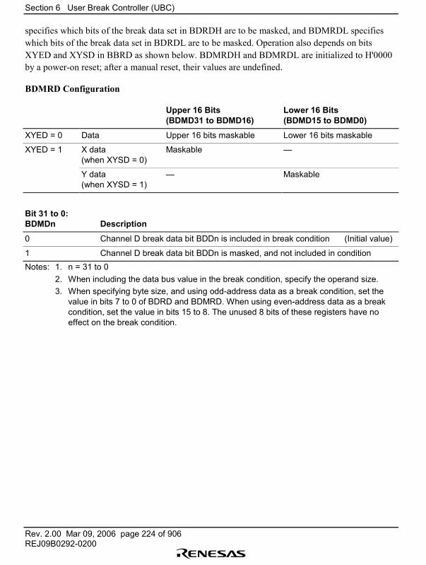
Section 6 User Break Controller (UBC)
Rev. 2.00 Mar 09, 2006 page 224 of 906REJ09B0292-0200
specifies which bits of the break data set in BDRDH are to be masked, and BDMRDL specifieswhich bits of the break data set in BDRDL are to be masked. Operation also depends on bitsXYED and XYSD in BBRD as shown below. BDMRDH and BDMRDL are initialized to H'0000by a power-on reset; after a manual reset, their values are undefined.
BDMRD Configuration
Upper 16 Bits(BDMD31 to BDMD16)
Lower 16 Bits(BDMD15 to BDMD0)
XYED = 0 Data Upper 16 bits maskable Lower 16 bits maskable
XYED = 1 X data(when XYSD = 0)
Maskable �
Y data(when XYSD = 1)
� Maskable
Bit 31 to 0:BDMDn Description
0 Channel D break data bit BDDn is included in break condition (Initial value)
1 Channel D break data bit BDDn is masked, and not included in conditionNotes: 1. n = 31 to 0
2. When including the data bus value in the break condition, specify the operand size.3. When specifying byte size, and using odd-address data as a break condition, set the
value in bits 7 to 0 of BDRD and BDMRD. When using even-address data as a breakcondition, set the value in bits 15 to 8. The unused 8 bits of these registers have noeffect on the break condition.
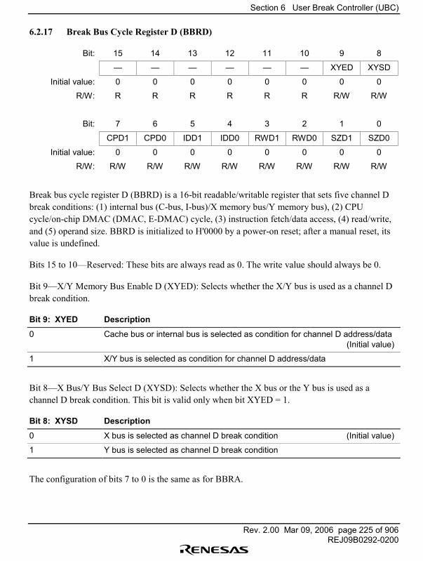
Section 6 User Break Controller (UBC)
Rev. 2.00 Mar 09, 2006 page 225 of 906REJ09B0292-0200
6.2.17 Break Bus Cycle Register D (BBRD)
Bit: 15 14 13 12 11 10 9 8
� � � � � � XYED XYSD
Initial value: 0 0 0 0 0 0 0 0
R/W: R R R R R R R/W R/W
Bit: 7 6 5 4 3 2 1 0
CPD1 CPD0 IDD1 IDD0 RWD1 RWD0 SZD1 SZD0
Initial value: 0 0 0 0 0 0 0 0
R/W: R/W R/W R/W R/W R/W R/W R/W R/W
Break bus cycle register D (BBRD) is a 16-bit readable/writable register that sets five channel Dbreak conditions: (1) internal bus (C-bus, I-bus)/X memory bus/Y memory bus), (2) CPUcycle/on-chip DMAC (DMAC, E-DMAC) cycle, (3) instruction fetch/data access, (4) read/write,and (5) operand size. BBRD is initialized to H'0000 by a power-on reset; after a manual reset, itsvalue is undefined.
Bits 15 to 10�Reserved: These bits are always read as 0. The write value should always be 0.
Bit 9�X/Y Memory Bus Enable D (XYED): Selects whether the X/Y bus is used as a channel Dbreak condition.
Bit 9: XYED Description
0 Cache bus or internal bus is selected as condition for channel D address/data(Initial value)
1 X/Y bus is selected as condition for channel D address/data
Bit 8�X Bus/Y Bus Select D (XYSD): Selects whether the X bus or the Y bus is used as achannel D break condition. This bit is valid only when bit XYED = 1.
Bit 8: XYSD Description
0 X bus is selected as channel D break condition (Initial value)
1 Y bus is selected as channel D break condition
The configuration of bits 7 to 0 is the same as for BBRA.
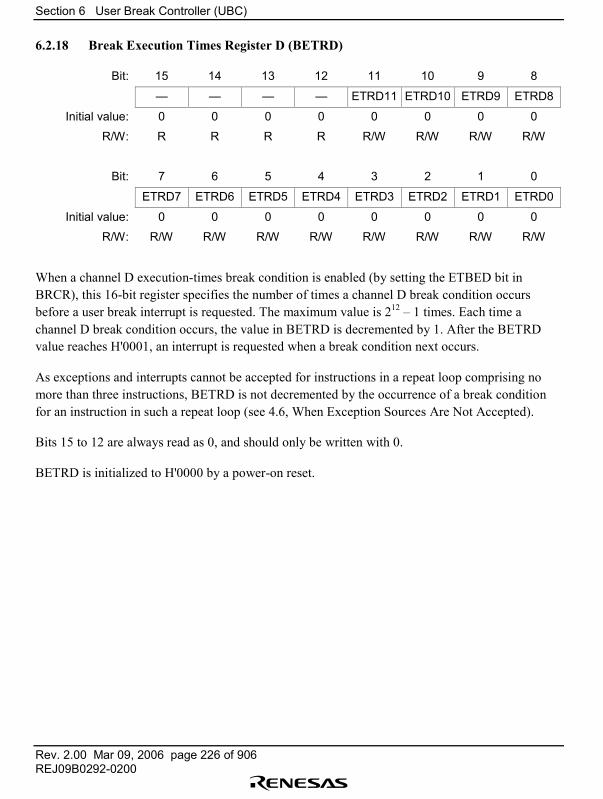
Section 6 User Break Controller (UBC)
Rev. 2.00 Mar 09, 2006 page 226 of 906REJ09B0292-0200
6.2.18 Break Execution Times Register D (BETRD)
Bit: 15 14 13 12 11 10 9 8
� � � � ETRD11 ETRD10 ETRD9 ETRD8
Initial value: 0 0 0 0 0 0 0 0
R/W: R R R R R/W R/W R/W R/W
Bit: 7 6 5 4 3 2 1 0
ETRD7 ETRD6 ETRD5 ETRD4 ETRD3 ETRD2 ETRD1 ETRD0
Initial value: 0 0 0 0 0 0 0 0
R/W: R/W R/W R/W R/W R/W R/W R/W R/W
When a channel D execution-times break condition is enabled (by setting the ETBED bit inBRCR), this 16-bit register specifies the number of times a channel D break condition occursbefore a user break interrupt is requested. The maximum value is 212 � 1 times. Each time achannel D break condition occurs, the value in BETRD is decremented by 1. After the BETRDvalue reaches H'0001, an interrupt is requested when a break condition next occurs.
As exceptions and interrupts cannot be accepted for instructions in a repeat loop comprising nomore than three instructions, BETRD is not decremented by the occurrence of a break conditionfor an instruction in such a repeat loop (see 4.6, When Exception Sources Are Not Accepted).
Bits 15 to 12 are always read as 0, and should only be written with 0.
BETRD is initialized to H'0000 by a power-on reset.
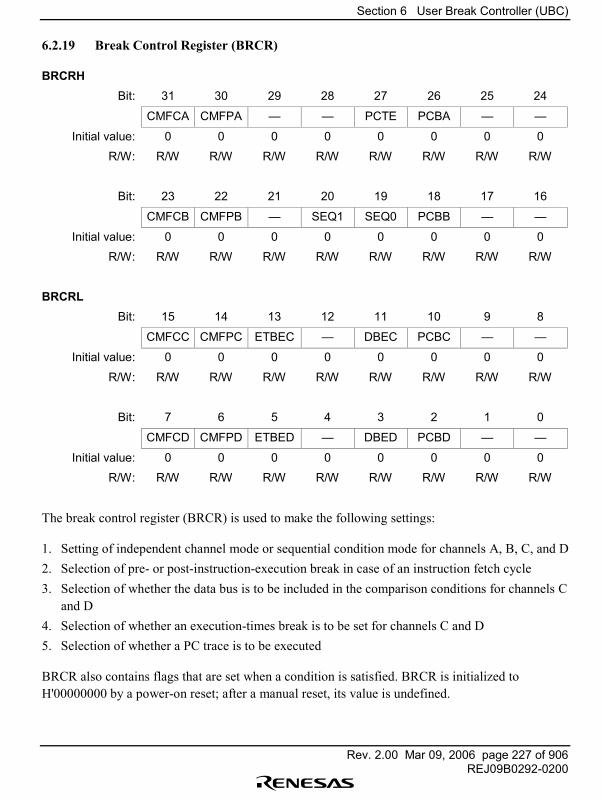
Section 6 User Break Controller (UBC)
Rev. 2.00 Mar 09, 2006 page 227 of 906REJ09B0292-0200
6.2.19 Break Control Register (BRCR)
BRCRHBit: 31 30 29 28 27 26 25 24
CMFCA CMFPA � � PCTE PCBA � �
Initial value: 0 0 0 0 0 0 0 0
R/W: R/W R/W R/W R/W R/W R/W R/W R/W
Bit: 23 22 21 20 19 18 17 16
CMFCB CMFPB � SEQ1 SEQ0 PCBB � �
Initial value: 0 0 0 0 0 0 0 0
R/W: R/W R/W R/W R/W R/W R/W R/W R/W
BRCRLBit: 15 14 13 12 11 10 9 8
CMFCC CMFPC ETBEC � DBEC PCBC � �
Initial value: 0 0 0 0 0 0 0 0
R/W: R/W R/W R/W R/W R/W R/W R/W R/W
Bit: 7 6 5 4 3 2 1 0
CMFCD CMFPD ETBED � DBED PCBD � �
Initial value: 0 0 0 0 0 0 0 0
R/W: R/W R/W R/W R/W R/W R/W R/W R/W
The break control register (BRCR) is used to make the following settings:
1. Setting of independent channel mode or sequential condition mode for channels A, B, C, and D2. Selection of pre- or post-instruction-execution break in case of an instruction fetch cycle3. Selection of whether the data bus is to be included in the comparison conditions for channels C
and D4. Selection of whether an execution-times break is to be set for channels C and D5. Selection of whether a PC trace is to be executed
BRCR also contains flags that are set when a condition is satisfied. BRCR is initialized toH'00000000 by a power-on reset; after a manual reset, its value is undefined.

Section 6 User Break Controller (UBC)
Rev. 2.00 Mar 09, 2006 page 228 of 906REJ09B0292-0200
Bit 31�CPU Condition Match Flag A (CMFCA): This flag is set to 1 when a CPU bus cyclecondition, among the break conditions set for channel A, is satisfied. This flag is not cleared to 0(if the flag setting is to be checked again after it has once been set, the flag must be cleared by awrite).
Bit 31: CMFCA Description
0 User break interrupt has not been generated by a channel A CPU cyclecondition (Initial value)
1 User break interrupt has been generated by a channel A CPU cycle condition
Bit 30�DMAC Condition Match Flag A (CMFPA): This flag is set to 1 when an on-chip DMACbus cycle condition, among the break conditions set for channel A, is satisfied. This flag is notcleared to 0 (if the flag setting is to be checked again after it has once been set, the flag must becleared by a write).
Bit 30: CMFPA Description
0 User break interrupt has not been generated by a channel A on-chip DMACcycle condition (Initial value)
1 User break interrupt has been generated by a channel A on-chip DMAC cyclecondition
Bits 29 and 28�Reserved: These bits are always read as 0. The write value should always be 0.
Bit 27�PC Trace Enable (PCTE): Selects whether a PC trace is to be executed.
Bit 27: PCTE Description
0 PC trace is not executed (Initial value)
1 PC trace is executed
Bit 26�PC Break Select A (PCBA): Selects whether a channel A instruction fetch cycle break iseffected before or after execution of the instruction.
Bit 26: PCBA Description
0 Channel A instruction fetch cycle break is effected before instruction execution(Initial value)
1 Channel A instruction fetch cycle break is effected after instruction execution
Bits 25 and 24�Reserved: These bits are always read as 0. The write value should always be 0.
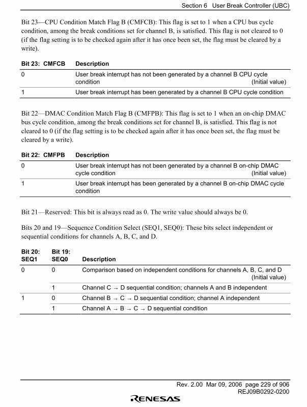
Section 6 User Break Controller (UBC)
Rev. 2.00 Mar 09, 2006 page 229 of 906REJ09B0292-0200
Bit 23�CPU Condition Match Flag B (CMFCB): This flag is set to 1 when a CPU bus cyclecondition, among the break conditions set for channel B, is satisfied. This flag is not cleared to 0(if the flag setting is to be checked again after it has once been set, the flag must be cleared by awrite).
Bit 23: CMFCB Description
0 User break interrupt has not been generated by a channel B CPU cyclecondition (Initial value)
1 User break interrupt has been generated by a channel B CPU cycle condition
Bit 22�DMAC Condition Match Flag B (CMFPB): This flag is set to 1 when an on-chip DMACbus cycle condition, among the break conditions set for channel B, is satisfied. This flag is notcleared to 0 (if the flag setting is to be checked again after it has once been set, the flag must becleared by a write).
Bit 22: CMFPB Description
0 User break interrupt has not been generated by a channel B on-chip DMACcycle condition (Initial value)
1 User break interrupt has been generated by a channel B on-chip DMAC cyclecondition
Bit 21�Reserved: This bit is always read as 0. The write value should always be 0.
Bits 20 and 19�Sequence Condition Select (SEQ1, SEQ0): These bits select independent orsequential conditions for channels A, B, C, and D.
Bit 20:SEQ1
Bit 19:SEQ0 Description
0 0 Comparison based on independent conditions for channels A, B, C, and D(Initial value)
1 Channel C → D sequential condition; channels A and B independent
1 0 Channel B → C → D sequential condition; channel A independent
1 Channel A → B → C → D sequential condition
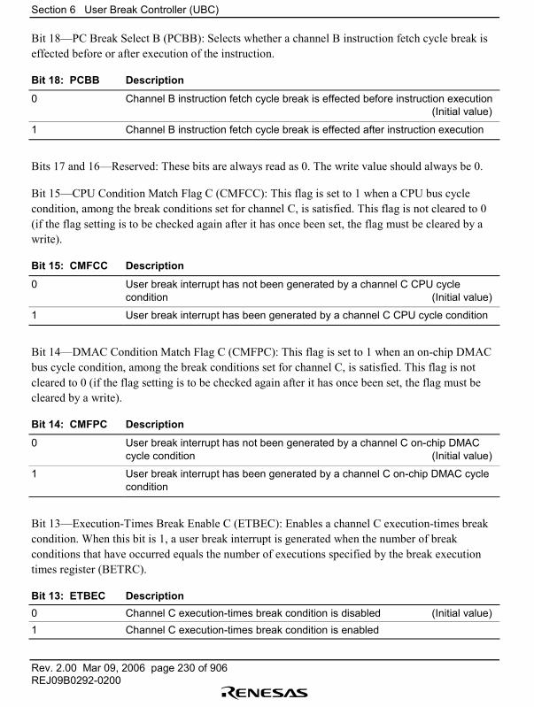
Section 6 User Break Controller (UBC)
Rev. 2.00 Mar 09, 2006 page 230 of 906REJ09B0292-0200
Bit 18�PC Break Select B (PCBB): Selects whether a channel B instruction fetch cycle break iseffected before or after execution of the instruction.
Bit 18: PCBB Description
0 Channel B instruction fetch cycle break is effected before instruction execution(Initial value)
1 Channel B instruction fetch cycle break is effected after instruction execution
Bits 17 and 16�Reserved: These bits are always read as 0. The write value should always be 0.
Bit 15�CPU Condition Match Flag C (CMFCC): This flag is set to 1 when a CPU bus cyclecondition, among the break conditions set for channel C, is satisfied. This flag is not cleared to 0(if the flag setting is to be checked again after it has once been set, the flag must be cleared by awrite).
Bit 15: CMFCC Description
0 User break interrupt has not been generated by a channel C CPU cyclecondition (Initial value)
1 User break interrupt has been generated by a channel C CPU cycle condition
Bit 14�DMAC Condition Match Flag C (CMFPC): This flag is set to 1 when an on-chip DMACbus cycle condition, among the break conditions set for channel C, is satisfied. This flag is notcleared to 0 (if the flag setting is to be checked again after it has once been set, the flag must becleared by a write).
Bit 14: CMFPC Description
0 User break interrupt has not been generated by a channel C on-chip DMACcycle condition (Initial value)
1 User break interrupt has been generated by a channel C on-chip DMAC cyclecondition
Bit 13�Execution-Times Break Enable C (ETBEC): Enables a channel C execution-times breakcondition. When this bit is 1, a user break interrupt is generated when the number of breakconditions that have occurred equals the number of executions specified by the break executiontimes register (BETRC).
Bit 13: ETBEC Description0 Channel C execution-times break condition is disabled (Initial value)1 Channel C execution-times break condition is enabled

Section 6 User Break Controller (UBC)
Rev. 2.00 Mar 09, 2006 page 231 of 906REJ09B0292-0200
Bit 12�Reserved: This bit is always read as 0. The write value should always be 0.
Bit 11�Data Break Enable C (DBEC): Selects whether a data bus condition is to be included inthe channel C break conditions.
Bit 11: DBEC Description
0 Data bus condition is not included in channel C conditions (Initial value)
1 Data bus condition is included in channel C conditions
Bit 10�PC Break Select C (PCBC): Selects whether a channel C instruction fetch cycle break iseffected before or after execution of the instruction.
Bit 10: PCBC Description
0 Channel C instruction fetch cycle break is effected before instruction execution(Initial value)
1 Channel C instruction fetch cycle break is effected after instruction execution
Bits 9 and 8�Reserved: These bits are always read as 0. The write value should always be 0.
Bit 7�CPU Condition Match Flag D (CMFCD): This flag is set to 1 when a CPU bus cyclecondition, among the break conditions set for channel D, is satisfied. This flag is not cleared to 0(if the flag setting is to be checked again after it has once been set, the flag must be cleared by awrite).
Bit 7: CMFCD Description
0 User break interrupt has not been generated by a channel D CPU cyclecondition (Initial value)
1 User break interrupt has been generated by a channel D CPU cycle condition
Bit 6�DMAC Condition Match Flag D (CMFPD): This flag is set to 1 when a DMAC bus cyclecondition, among the break conditions set for channel D, is satisfied. This flag is not cleared to 0(if the flag setting is to be checked again after it has once been set, the flag must be cleared by awrite).
Bit 6: CMFPD Description
0 User break interrupt has not been generated by a channel D on-chip DMACcycle condition (Initial value)
1 User break interrupt has been generated by a channel D on-chip DMAC cyclecondition
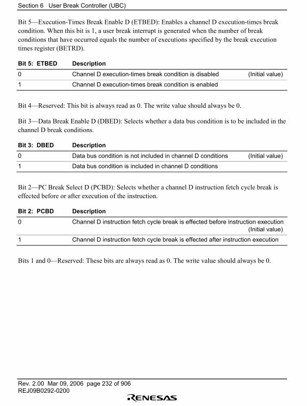
Section 6 User Break Controller (UBC)
Rev. 2.00 Mar 09, 2006 page 232 of 906REJ09B0292-0200
Bit 5�Execution-Times Break Enable D (ETBED): Enables a channel D execution-times breakcondition. When this bit is 1, a user break interrupt is generated when the number of breakconditions that have occurred equals the number of executions specified by the break executiontimes register (BETRD).
Bit 5: ETBED Description
0 Channel D execution-times break condition is disabled (Initial value)
1 Channel D execution-times break condition is enabled
Bit 4�Reserved: This bit is always read as 0. The write value should always be 0.
Bit 3�Data Break Enable D (DBED): Selects whether a data bus condition is to be included in thechannel D break conditions.
Bit 3: DBED Description
0 Data bus condition is not included in channel D conditions (Initial value)
1 Data bus condition is included in channel D conditions
Bit 2�PC Break Select D (PCBD): Selects whether a channel D instruction fetch cycle break iseffected before or after execution of the instruction.
Bit 2: PCBD Description
0 Channel D instruction fetch cycle break is effected before instruction execution(Initial value)
1 Channel D instruction fetch cycle break is effected after instruction execution
Bits 1 and 0�Reserved: These bits are always read as 0. The write value should always be 0.
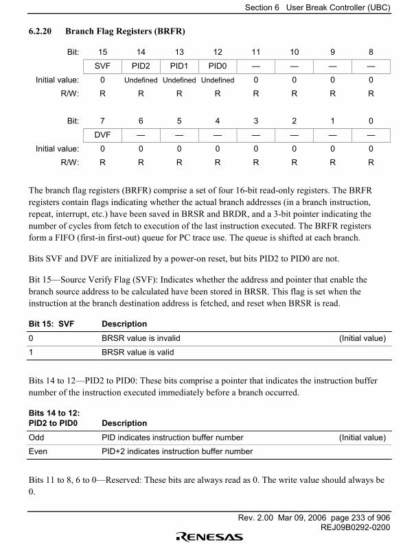
Section 6 User Break Controller (UBC)
Rev. 2.00 Mar 09, 2006 page 233 of 906REJ09B0292-0200
6.2.20 Branch Flag Registers (BRFR)
Bit: 15 14 13 12 11 10 9 8
SVF PID2 PID1 PID0 � � � �
Initial value: 0 Undefined Undefined Undefined 0 0 0 0
R/W: R R R R R R R R
Bit: 7 6 5 4 3 2 1 0
DVF � � � � � � �
Initial value: 0 0 0 0 0 0 0 0
R/W: R R R R R R R R
The branch flag registers (BRFR) comprise a set of four 16-bit read-only registers. The BRFRregisters contain flags indicating whether the actual branch addresses (in a branch instruction,repeat, interrupt, etc.) have been saved in BRSR and BRDR, and a 3-bit pointer indicating thenumber of cycles from fetch to execution of the last instruction executed. The BRFR registersform a FIFO (first-in first-out) queue for PC trace use. The queue is shifted at each branch.
Bits SVF and DVF are initialized by a power-on reset, but bits PID2 to PID0 are not.
Bit 15�Source Verify Flag (SVF): Indicates whether the address and pointer that enable thebranch source address to be calculated have been stored in BRSR. This flag is set when theinstruction at the branch destination address is fetched, and reset when BRSR is read.
Bit 15: SVF Description
0 BRSR value is invalid (Initial value)
1 BRSR value is valid
Bits 14 to 12�PID2 to PID0: These bits comprise a pointer that indicates the instruction buffernumber of the instruction executed immediately before a branch occurred.
Bits 14 to 12:PID2 to PID0 Description
Odd PID indicates instruction buffer number (Initial value)
Even PID+2 indicates instruction buffer number
Bits 11 to 8, 6 to 0�Reserved: These bits are always read as 0. The write value should always be0.

Section 6 User Break Controller (UBC)
Rev. 2.00 Mar 09, 2006 page 234 of 906REJ09B0292-0200
Bit 7�Destination Verify Flag (DVF): Indicates whether the branch source address has beenstored in BRDR. This flag is set when the instruction at the branch destination address is fetched,and reset when BRDR is read.
Bit 7: DVF Description
0 BRDR value is invalid (Initial value)
1 BRDR value is valid
See the PC trace description for the method of executing a PC trace using the branch sourceregisters (BRSR), branch destination registers (BRDR), and branch flag registers (BRFR).
6.2.21 Branch Source Registers (BRSR)
BRSRHBit: 31 30 29 28 27 26 25 24
BSA31 BSA30 BSA29 BSA28 BSA27 BSA26 BSA25 BSA24
Initial value: Undefined Undefined Undefined Undefined Undefined Undefined Undefined Undefined
R/W: R R R R R R R R
Bit: 23 22 21 20 19 18 17 16
BSA23 BSA22 BSA21 BSA20 BSA19 BSA18 BSA17 BSA16
Initial value: Undefined Undefined Undefined Undefined Undefined Undefined Undefined Undefined
R/W: R R R R R R R R
BRSRLBit: 15 14 13 12 11 10 9 8
BSA15 BSA14 BSA13 BSA12 BSA11 BSA10 BSA9 BSA8
Initial value: Undefined Undefined Undefined Undefined Undefined Undefined Undefined Undefined
R/W: R R R R R R R R
Bit: 7 6 5 4 3 2 1 0
BSA7 BSA6 BSA5 BSA4 BSA3 BSA2 BSA1 BSA0
Initial value: Undefined Undefined Undefined Undefined Undefined Undefined Undefined Undefined
R/W: R R R R R R R R
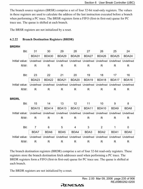
Section 6 User Break Controller (UBC)
Rev. 2.00 Mar 09, 2006 page 235 of 906REJ09B0292-0200
The branch source registers (BRSR) comprise a set of four 32-bit read-only registers. The valuesin these registers are used to calculate the address of the last instruction executed before a branchwhen performing a PC trace. The BRSR registers form a FIFO (first-in first-out) queue for PCtrace use. The queue is shifted at each branch.
The BRSR registers are not initialized by a reset.
6.2.22 Branch Destination Registers (BRDR)
BRDRHBit: 31 30 29 28 27 26 25 24
BDA31 BDA30 BDA29 BDA28 BDA27 BDA26 BDA25 BDA24
Initial value: Undefined Undefined Undefined Undefined Undefined Undefined Undefined Undefined
R/W: R R R R R R R R
Bit: 23 22 21 20 19 18 17 16
BDA23 BDA22 BDA21 BDA20 BDA19 BDA18 BDA17 BDA16
Initial value: Undefined Undefined Undefined Undefined Undefined Undefined Undefined Undefined
R/W: R R R R R R R R
BRDRLBit: 15 14 13 12 11 10 9 8
BDA15 BDA14 BDA13 BDA12 BDA11 BDA10 BDA9 BDA8
Initial value: Undefined Undefined Undefined Undefined Undefined Undefined Undefined Undefined
R/W: R R R R R R R R
Bit: 7 6 5 4 3 2 1 0
BDA7 BDA6 BDA5 BDA4 BDA3 BDA2 BDA1 BDA0
Initial value: Undefined Undefined Undefined Undefined Undefined Undefined Undefined Undefined
R/W: R R R R R R R R
The branch destination registers (BRDR) comprise a set of four 32-bit read-only registers. Theseregisters store the branch destination fetch addresses used when performing a PC trace. TheBRDR registers form a FIFO (first-in first-out) queue for PC trace use. The queue is shifted ateach branch.
The BRDR registers are not initialized by a reset.
Section 6 User Break Controller (UBC)
Rev. 2.00 Mar 09, 2006 page 236 of 906REJ09B0292-0200
6.3 Operation
6.3.1 User Break Operation Sequence
The sequence of operations from setting of break conditions to user break interrupt exceptionhandling is described below.
1. Set the break address in the break address register (BARA/BARB/BARC/BARD), the bits tobe masked in the break address mask register (BAMRA/BAMRB/BAMRC/BAMRD), thebreak bits in the break data register (BDRC/BDRD), and the data to be masked in the breakdata mask register (BDMRC/BDMRD).Set the break bus conditions in the break bus cycle register (BBRA/BBRB/BBRC/BBRD).Make three settings�CPU cycle/on-chip DMAC cycle select, instruction fetch/data accessselect, and read/write select�for each of BBRA, BBRB, BBRC, and BBRD. A user breakinterrupt will not be generated for a channel for which any one of these settings is 00.Set the respective conditions in the corresponding BRCR register bits.
2. When a set condition is satisfied, the UBC sends a user break interrupt request to the interruptcontroller (INTC). The CPU condition match flag (CMFCA/CMFCB/CMFCC/CMFCD) andDMAC condition match flag (CMFPA/CMFPB/CMFPC/CMFPD) is also set for the matchedcondition for the respective channel.
3. The INTC determines the priority of the user break interrupt. As the priority level of a userbreak interrupt is 15, the interrupt is accepted if the level set in the interrupt mask bits (I3 to I0)in the status register (SR) is 14 or less. If the level set in bits I3 to I0 is 15, the user breakinterrupt is not accepted, but is held pending until it can be. For details of prioritydetermination, see section 5, Interrupt Controller (INTC).
4. If the user break interrupt is accepted after its priority is determined, the CPU begins userbreak interrupt exception handling.
5. Whether a set condition is matched or not can be ascertained from the respective conditionmatch flag (CMFCA, CMFPA, CMFCB, CMFPB, CMFCC, CMFPC, CMFCD, or CMFPD).These flags are set by a match with the set condition, but are not reset. Therefore, if the settingof a particular flag is to be checked again, the flag must be cleared by writing 0.When an execution-times break is specified for channel C or D, the CMFCC, CMFPC,CMFCD, or CMFPD flag is set when the number of executions matches the number ofexecutions specified by BETRC or BETRD.
Section 6 User Break Controller (UBC)
Rev. 2.00 Mar 09, 2006 page 237 of 906REJ09B0292-0200
6.3.2 Instruction Fetch Cycle Break
1. If a CPU/instruction fetch/read/word setting is made in the break bus cycle register (BBRA,BBRB, BBRC, or BBRD), a CPU instruction fetch cycle can be selected as a break condition.In this case, it is possible to specify whether the break is to be effected before or afterexecution of the relevant instruction by means of the PCBA/PCBB/PCBC/PCBD bit in thebreak control register (BRCR).
2. In the case of an instruction for which pre-execution is set as the break condition, the break isperformed when it has been confirmed that the instruction has been fetched and is to beexecuted. Consequently, a break cannot be set for an overrun-fetched instruction (aninstruction fetched but not executed in the event of a branch or interrupt transition). If a breakis set for the delay slot of a delayed branch instruction, or for the instruction following aninstruction for which interrupts are prohibited, such as LCD, an interrupt is generated beforeexecution of the next instruction at which interrupts are accepted.
3. With the post-execution condition, an interrupt is generated after execution of the instructionset as the break condition, and before execution of the following instruction. As in 2 above, abreak cannot be set for an overrun-fetched instruction. If a break is set for a delayed branchinstruction, or for an instruction for which interrupts are prohibited, such as LCD, an interruptis generated before execution of the next instruction at which interrupts are accepted.
4. When an instruction fetch cycle is set for channel C or D, break data register C (BDRC) orbreak data register D (BDRD) is ignored. Therefore, break data need not be set for aninstruction fetch cycle break.
5. When an instruction fetch cycle is set, the start address at which that instruction is locatedshould be set for the break. A break will not occur if a different address is set. Also, a breakwill not occur if the address of the lower word of a 32-bit instruction is set.

Section 6 User Break Controller (UBC)
Rev. 2.00 Mar 09, 2006 page 238 of 906REJ09B0292-0200
6.3.3 Data Access Cycle Break
1. Memory cycles for which a CPU data access break can be set are memory cycles due toinstructions and stack operations and vector reads when exception handling is executed. ACPU data access break cannot be set for a vector fetch cycle of an external vector interrupt, forburst write of a synchronous DRAM, or for a dammy access cycle of a single read.
2. Table 6.2 shows the bits of the break address register and the address bus that are compared foreach operand size to determine whether a break condition has been matched.
Table 6.2 Data Access Cycle Address and Operand Size Comparison Conditions
Access Size Compared Address Bits
Longword Bits 31 to 2 of break address register compared with bits 31 to 2 of address bus
Word Bits 31 to 1 of break address register compared with bits 31 to 1 of address bus
Byte Bits 31 to 0 of break address register compared with bits 31 to 0 of address bus
This means, for example, that if address H'00001003 is set without specifying a size condition,bus cycles that satisfy the break conditions are as follows (assuming that all other conditionsare satisfied):Longword access at address H'00001000Word access at address H'00001002Byte access at address H'00001003
3. When data value is included in break condition in channel CWhen the data value is included in the break conditions, specify longword, word, or byte as theoperand size in break bus cycle register C (BBRC). When the data value is included in thebreak conditions, a break interrupt is generated on a match of the address condition and thedata condition.When byte data is specified, set the same data in the two bytes comprising bits 15 to 8 and bits7 to 0 in break data register C (BDRC) and break data mask register C (BDMRC). If word orbyte is designated, bits 31 to 16 of BDRC and BDMRC are ignored.Similar conditions apply when the data value is included in the break conditions for channel D.
Section 6 User Break Controller (UBC)
Rev. 2.00 Mar 09, 2006 page 239 of 906REJ09B0292-0200
6.3.4 Saved Program Counter (PC) Value
1. When instruction fetch (pre-instruction-execution) is set as break conditionThe program counter (PC) value saved to the stack in user break interrupt exception handlingis the address of the instruction for which the break condition matched. In this case, the fetchedinstruction is not executed, a user break interrupt being generated prior to its execution. If asetting is made for an instruction following an instruction for which interrupts are prohibited,the break is effected before execution of the next instruction at which interrupts are accepted,so that the saved PC value is the address at which the break occurs.
2. When instruction fetch (post-instruction-execution) is set as break conditionThe program counter (PC) value saved to the stack in user break interrupt exception handlingis the address of the next instruction to be executed after the instruction for which the breakcondition matched. In this case, the fetched instruction is executed, and a user break interruptis generated before execution of the next instruction. However, if a setting is made for aninstruction for which interrupts are prohibited, the break is effected before execution of thenext instruction at which interrupts are accepted, so that the saved PC value is the address atwhich the break occurs.
3. When data access (CPU/on-chip DMAC) is set as break conditionThe value saved is the start address of the next instruction after the instruction for whichexecution has been completed when user break exception handling is initiated.When data access (CPU/on-chip DMAC) is set as a break condition, the point at which thebreak is to be made cannot be specified. A break is effected before execution of the instructionabout to be fetched around the time of the break data access.
6.3.5 X Memory Bus or Y Memory Bus Cycle Break
A break condition for an X bus cycle or Y bus cycle can only be specified for channel C or D.When XYEC in BBRC or XYED in BBRD is set to 1, break addresses and break data on the Xmemory bus or Y memory bus are selected. Either the X memory bus or the Y memory bus mustbe selected with the XYSC bit in BBRC or the XYSD bit in BBRD; the X and Y memory busescannot both be included in the break conditions at the same time. The break conditions are appliedto X memory bus cycles or Y memory bus cycles by setting the CPU bus master, data accesscycle, read or write access, and word operand size or no operand size specification.
When an X memory address is selected as a break condition, specify the X memory address in theupper 16 bits of BARC and BAMRC or BARD and BAMRD; when a Y memory address isselected, specify the Y memory address in the lower 16 bits of BARC and BAMRC or BARD andBAMRD. The same method is used to specify X memory data or Y memory data for BDRC andBDMRC or BDRD and BMRD.
Section 6 User Break Controller (UBC)
Rev. 2.00 Mar 09, 2006 page 240 of 906REJ09B0292-0200
6.3.6 Sequential Break
Channel C to Channel D: When SEQ1 in BRCR is set to 0 and SEQ0 is set to 1, a sequentialbreak occurs when the conditions are met for channel C and then channel D, in that order. Thiscauses the BRCR condition match flag for each channel to be set to 1.
If the break conditions for channels C and D are met at the same time, and the conditions had notalready been met for channel C, the conditions are considered to be met for channel C alone, in thesame manner as if the conditions were met for channel C first. Also, if the conditions for channelC have already been met when the break conditions for channels C and D are met at the sametime, the conditions for channel D are considered to be met and a break occurs.
Channel B to Channel C to Channel D: When SEQ1 in BRCR is set to 1 and SEQ0 is set to 0, asequential break occurs when the conditions are met for channel B, channel C, and then channelD, in that order. This causes the BRCR condition match flag for each channel to be set to 1.
If the break conditions for channels B and C are met at the same time, and the conditions had notalready been met for channel B, the conditions are considered to be met for channel B. Also, if theconditions for channel B have already been met when the break conditions for channels B and Care met at the same time, the conditions for channel C are considered to be met.
If the break conditions for channels C and D are met at the same time, and the conditions had notalready been met for channel C, the conditions are considered to be met for channel C. Also, if theconditions for channel C have already been met when the break conditions for channels C and Dare met at the same time, the conditions for channel D are considered to be met and a breakoccurs.
Channel A to Channel B to Channel C to Channel D: When SEQ1 in BRCR is set to 1 andSEQ0 is set to 1, a sequential break occurs when the conditions are met for channel A, channel B,channel C, and then channel D, in that order. This causes the BRCR condition match flag for eachchannel to be set to 1.
If the break conditions for channels A and B are met at the same time, and the conditions had notalready been met for channel A, the conditions are considered to be met for channel A. Also, if theconditions for channel A have already been met when the break conditions for channels A and Bare met at the same time, the conditions for channel B are considered to be met.
If the break conditions for channels B and C are met at the same time, and the conditions had notalready been met for channel B, the conditions are considered to be met for channel B. Also, if theconditions for channel B have already been met when the break conditions for channels B and Care met at the same time, the conditions for channel C are considered to be met.
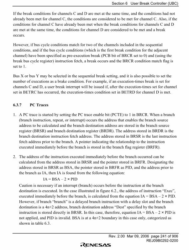
Section 6 User Break Controller (UBC)
Rev. 2.00 Mar 09, 2006 page 241 of 906REJ09B0292-0200
If the break conditions for channels C and D are met at the same time, and the conditions had notalready been met for channel C, the conditions are considered to be met for channel C. Also, if theconditions for channel C have already been met when the break conditions for channels C and Dare met at the same time, the conditions for channel D are considered to be met and a breakoccurs.
However, if bus cycle conditions match for two of the channels included in the sequentialconditions, and if the bus cycle conditions (which is the first break condition for the adjacentchannel) have been specified as pre-execution break (PCB bit of BRCR set to 0) and (using thebreak bus cycle register) instruction fetch, a break occurs and the BRCR condition match flag isset to 1.
Bus X or bus Y may be selected in the sequential break setting, and it is also possible to set thenumber of executions as a brake condition. For example, if an execution-times break is set forchannels C and D, a user break interrupt will be issued if, after the execution-times set for channelset in BETRC has occurred, the execution-times condition set in BETRD for channel D is met.
6.3.7 PC Traces
1. A PC trace is started by setting the PC trace enable bit (PCTE) to 1 in BRCR. When a branch(branch instruction, repeat, or interrupt) occurs the address that enables the branch sourceaddress to be calculated and the branch destination address are stored in the branch sourceregister (BRSR) and branch destination register (BRDR). The address stored in BRDR is thebranch destination instruction fetch address. The address stored in BRSR is the last instructionfetch address prior to the branch. A pointer indicating the relationship to the instructionexecuted immediately before the branch is stored in the branch flag register (BRFR).
2. The address of the instruction executed immediately before the branch occurred can becalculated from the address stored in BRSR and the pointer stored in BRFR. Designating theaddress stored in BRSR as BSA, the pointer stored in BRFR as PID, and the address prior tothe branch as IA, then IA is found from the following equation:
IA = BSA � 2 × PIDCaution is necessary if an interrupt (branch) occurs before the instruction at the branchdestination is executed. In the case illustrated in figure 6.2., the address of instruction �Exec�,executed immediately before the branch, is calculated from the equation IA = BSA � 2 × PID.However, if branch �branch� is a delayed branch instruction with a delay slot and the branchdestination is a 4n+2 address, branch destination address �Dest� specified by the branchinstruction is stored directly in BRSR. In this case, therefore, equation IA = BSA � 2 × PID isnot applied, and PID is invalid. BSA is at a 4n+2 boundary in this case only, categorized asshown in table 6.3.
Section 6 User Break Controller (UBC)
Rev. 2.00 Mar 09, 2006 page 242 of 906REJ09B0292-0200
Exec:
Dest:
Int:
branch Dest
instr; Not executed
Interrupt
interrupt routine
Figure 6.2 When Interrupt Occurs before Branch Instruction Is Executed
Table 6.3 BSA Values Stored in Exception Handling before Execution of BranchDestination Instruction
BranchBranch Destination(Dest) BSA
Branch Source Address Calculable by Meansof BRSR and BRFR
Delay 4n 4n Exec = IA = BSA � 2 × PID
4n + 2 4n + 2 Dest = BSA
No delay 4n or 4n + 2 4n Exec = IA = BSA � 2 × PID
If PID is an odd number, the value incremented by 2 indicates the instruction buffer, but theequations in the table do not take this into account. Therefore, the calculation can be performedusing the values of BSA stored in BRSR and PID stored in BRFR.
3. The location indicated by the address before branch occurrence, IA, differs according to thekind of branch.a. Branch instruction: Branch instruction addressb. Repeat loop: 2nd instruction from last in repeat loop
Repeat_Start: inst (1); → BRDRinst(2);
:
inst (n-1); → Address calculated from BRSR and BRFRRepeat End: inst (n);
c. Interrupt: Instruction executed immediately before interruptThe address of the first instruction in the interrupt routine is stored in BRDR.
In a repeat loop consisting of no more than three instructions, an instruction fetch cycle is notgenerated. As the branch destination address is unknown, a PC trace cannot be performed.
Section 6 User Break Controller (UBC)
Rev. 2.00 Mar 09, 2006 page 243 of 906REJ09B0292-0200
4. BRSR, BRDR, and BRFR have a four-queue structure. When the stored address is read in a PCtrace, the read is performed from the head of the queue. Reads should be performed in theorder BRFR, BRSR, BRDR. After BRDR is read, the queue shifts by one. Use longwordaccess to read BRSR and BRDR.
6.3.8 Examples of Use
CPU Instruction Fetch Cycle Break Condition Settings
A. Register settings: BARA = H'00000404 / BAMRA = H'00000000 / BBRA = H'0054BARB = H'00003080 / BAMRB = H'0000007F / BBRB = H'0054BARC = H'00008010 / BAMRC = H'00000006 / BBRC = H'0054BDRC = H'00000000 / BDMRC = H'00000000BARD =H'0000FF04 / BAMRD = H'00000000 / BBRD = H'0054BDRD = H'00000000 / BDMRD = H'00000000BRCR = H'04000400
Set conditions: All channels independent
Channel A: Address: H'00000404; address mask: H'00000000Bus cycle: CPU, instruction fetch (post-execution),
read (operand size not included in conditions)
Channel B: Address: H'00003080; address mask: H'0000007FBus cycle: CPU, instruction fetch (pre-execution),
read (operand size not included in conditions)
Channel C: Address: H'00008010; address mask: H'00000006Data: H'00000000; data mask: H'00000000Bus cycle: CPU, instruction fetch (post-execution),
read (operand size not included in conditions)
Channel D: Address: H'0000FF04; address mask: H'00000000Data: H'00000000; data mask: H'00000000Bus cycle: CPU, instruction fetch (pre-execution),
read (operand size not included in conditions)
A user break interrupt is generated after execution of the instruction at address H'00000404,before execution of instructions at addresses H'00003080 to H'000030FF, after execution ofinstructions at addresses H'00008010 to H'00008016, or before execution of the instruction ataddress H'0000FF04.
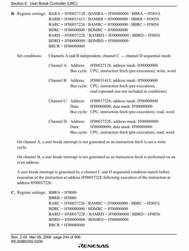
Section 6 User Break Controller (UBC)
Rev. 2.00 Mar 09, 2006 page 244 of 906REJ09B0292-0200
B. Register settings: BARA = H'00027128 / BAMRA = H'00000000 / BBRA = H'005ABARB = H'00031415 / BAMRB = H'00000000 / BBRB = H'0054BARC = H'00037226 / BAMRC = H'00000000 / BBRC = H'0056BDRC = H'00000000 / BDMRC = H'00000000BARD = H'0003722E / BAMRD = H'00000000 / BBRD = H'0056BDRD = H'00000000 / BDMRD = H'00000000BRCR = H'00080000
Set conditions: Channels A and B independent, channel C → channel D sequential mode
Channel A: Address: H'00027128; address mask: H'00000000Bus cycle: CPU, instruction fetch (pre-execution), write, word
Channel B: Address: H'00031415; address mask: H'00000000Bus cycle: CPU, instruction fetch (pre-execution),
read (operand size not included in conditions)
Channel C: Address: H'00037226; address mask: H'00000000Data: H'00000000; data mask: H'00000000Bus cycle: CPU, instruction fetch (pre-execution), read, word
Channel D: Address: H'0003722E; address mask: H'00000000Data: H'00000000; data mask: H'00000000Bus cycle: CPU, instruction fetch (pre-execution), read, word
On channel A, a user break interrupt is not generated as an instruction fetch is not a writecycle.
On channel B, a user break interrupt is not generated as an instruction fetch is performed on aneven address.
A user break interrupt is generated by a channel C and D sequential condition match beforeexecution of the instruction at address H'0003722E following execution of the instruction ataddress H'00037226.
C. Register settings: BBRA = H'0000BBRB = H'0000BARC = H'00037226 / BAMRC = H'00000000 / BBRC = H'005ABDRC = H'00000000 / BDMRC = H'00000000BARD = H'0003722E / BAMRD = H'00000000 / BBRD = H'0056BDRD = H'00000000 / BDMRD = H'00000000BRCR = H'00080000
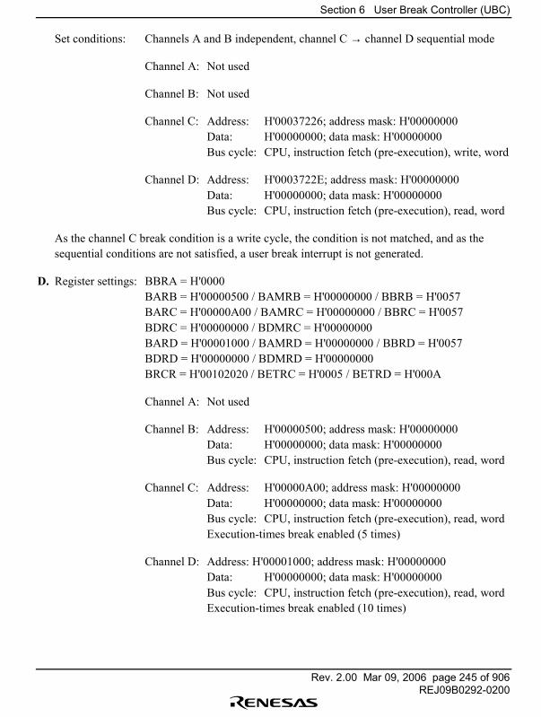
Section 6 User Break Controller (UBC)
Rev. 2.00 Mar 09, 2006 page 245 of 906REJ09B0292-0200
Set conditions: Channels A and B independent, channel C → channel D sequential mode
Channel A: Not used
Channel B: Not used
Channel C: Address: H'00037226; address mask: H'00000000Data: H'00000000; data mask: H'00000000Bus cycle: CPU, instruction fetch (pre-execution), write, word
Channel D: Address: H'0003722E; address mask: H'00000000Data: H'00000000; data mask: H'00000000Bus cycle: CPU, instruction fetch (pre-execution), read, word
As the channel C break condition is a write cycle, the condition is not matched, and as thesequential conditions are not satisfied, a user break interrupt is not generated.
D. Register settings: BBRA = H'0000BARB = H'00000500 / BAMRB = H'00000000 / BBRB = H'0057BARC = H'00000A00 / BAMRC = H'00000000 / BBRC = H'0057BDRC = H'00000000 / BDMRC = H'00000000BARD = H'00001000 / BAMRD = H'00000000 / BBRD = H'0057BDRD = H'00000000 / BDMRD = H'00000000BRCR = H'00102020 / BETRC = H'0005 / BETRD = H'000A
Channel A: Not used
Channel B: Address: H'00000500; address mask: H'00000000Data: H'00000000; data mask: H'00000000Bus cycle: CPU, instruction fetch (pre-execution), read, word
Channel C: Address: H'00000A00; address mask: H'00000000Data: H'00000000; data mask: H'00000000Bus cycle: CPU, instruction fetch (pre-execution), read, wordExecution-times break enabled (5 times)
Channel D: Address: H'00001000; address mask: H'00000000Data: H'00000000; data mask: H'00000000Bus cycle: CPU, instruction fetch (pre-execution), read, wordExecution-times break enabled (10 times)

Section 6 User Break Controller (UBC)
Rev. 2.00 Mar 09, 2006 page 246 of 906REJ09B0292-0200
After the instruction at address H'0000500 is executed, and the instruction at addressH'00000A00 is executed five times, a user break interrupt is generated after the instruction ataddress H'00001000 has been executed nine times, but before it is executed a tenth time.
CPU Data Access Cycle Break Condition Settings
Register settings: BARA = H'00123456 / BAMRA = H'00000000 / BBRA = H'0064BARB = H'01000000 / BAMRB = H'00000000 / BBRB = H'0066BARC = H'000ABCDE / BAMRC = H'000000FF / BBRC = H'006ABDRC = H'0000A512 / BDMRC = H'00000000BARD = H'1001E000 / BAMRD = H'FFFF0000 / BBRD = H'036ABDRD = H'00004567 / BDMRD = H'00000000BRCR = H'00000808
Set conditions: All channels independent
Channel A: Address: H'00123456; address mask: H'00000000Bus cycle: CPU, data access, read (operand size not included
in conditions)
Channel B: Address: H'01000000; address mask: H'00000000Bus cycle: CPU, data access, read, word
Channel C: Address: H'000ABCDE; address mask: H'00000000Data: H'0000A512; data mask: H'00000000Bus cycle: CPU, data access, write, word
Channel D: Y address: H'1001E000; address mask: H'FFFF0000Data: H'00004567; data mask: H'00000000Bus cycle: CPU, data access, write, word
On channel A, a user break interrupt is generated by a longword read at address H'00123456, aword read at address H'00123456, or a byte read at address H'00123456.
On channel B, a user break interrupt is generated by a word read at address H'01000000.
On channel C, a user break interrupt is generated when H'A512 is written by word access to anaddress from H'000ABC00 to H'000ABCFE.
On channel D, a user break interrupt is generated when H'4567 is written by word access toaddress H'1001E000 in Y memory space.
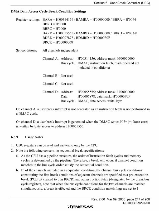
Section 6 User Break Controller (UBC)
Rev. 2.00 Mar 09, 2006 page 247 of 906REJ09B0292-0200
DMA Data Access Cycle Break Condition Settings
Register settings: BARA = H'00314156 / BAMRA = H'00000000 / BBRA = H'0094BBRB = H'0000BBRC = H'0000BARD = H'00055555 / BAMRD = H'00000000 / BBRD = H'00A9BDRD = H'00007878 / BDMRD = H'00000F0FBRCR = H'00000008
Set conditions: All channels independent
Channel A: Address: H'00314156; address mask: H'00000000Bus cycle: DMAC, instruction fetch, read (operand not
included in conditions)
Channel B: Not used
Channel C: Not used
Channel D: Address: H'00055555; address mask: H'00000000Data: H'00007878; data mask: H'00000F0FBus cycle: DMAC, data access, write, byte
On channel A, a user break interrupt is not generated as an instruction fetch is not performed ina DMAC cycle.
On channel D, a user break interrupt is generated when the DMAC writes H'7* (*: Don't care)is written by byte access to address H'00055555.
6.3.9 Usage Notes
1. UBC registers can be read and written to only by the CPU.2. Note the following concerning sequential break specifications:
a. As the CPU has a pipeline structure, the order of instruction fetch cycles and memorycycles is determined by the pipeline. Therefore, a break will occur if channel conditionmatches in the bus cycle order satisfy the sequential condition.
b. If, of the channels included in a sequential condition, the channel bus cycle conditionsconstituting the first break conditions of adjacent channels are specified as a pre-executionbreak (PCB bit cleared to 0 in BRCR) and an instruction fetch (designated by the break buscycle register), note that when the bus cycle conditions for the two channels are matchedsimultaneously, a break is effected and the BRCR condition match flags are set to 1.
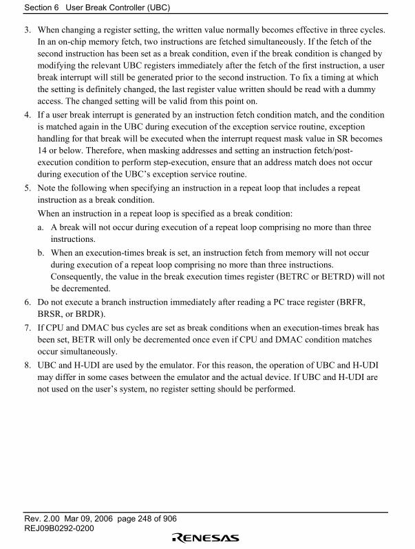
Section 6 User Break Controller (UBC)
Rev. 2.00 Mar 09, 2006 page 248 of 906REJ09B0292-0200
3. When changing a register setting, the written value normally becomes effective in three cycles.In an on-chip memory fetch, two instructions are fetched simultaneously. If the fetch of thesecond instruction has been set as a break condition, even if the break condition is changed bymodifying the relevant UBC registers immediately after the fetch of the first instruction, a userbreak interrupt will still be generated prior to the second instruction. To fix a timing at whichthe setting is definitely changed, the last register value written should be read with a dummyaccess. The changed setting will be valid from this point on.
4. If a user break interrupt is generated by an instruction fetch condition match, and the conditionis matched again in the UBC during execution of the exception service routine, exceptionhandling for that break will be executed when the interrupt request mask value in SR becomes14 or below. Therefore, when masking addresses and setting an instruction fetch/post-execution condition to perform step-execution, ensure that an address match does not occurduring execution of the UBC�s exception service routine.
5. Note the following when specifying an instruction in a repeat loop that includes a repeatinstruction as a break condition.When an instruction in a repeat loop is specified as a break condition:a. A break will not occur during execution of a repeat loop comprising no more than three
instructions.b. When an execution-times break is set, an instruction fetch from memory will not occur
during execution of a repeat loop comprising no more than three instructions.Consequently, the value in the break execution times register (BETRC or BETRD) will notbe decremented.
6. Do not execute a branch instruction immediately after reading a PC trace register (BRFR,BRSR, or BRDR).
7. If CPU and DMAC bus cycles are set as break conditions when an execution-times break hasbeen set, BETR will only be decremented once even if CPU and DMAC condition matchesoccur simultaneously.
8. UBC and H-UDI are used by the emulator. For this reason, the operation of UBC and H-UDImay differ in some cases between the emulator and the actual device. If UBC and H-UDI arenot used on the user�s system, no register setting should be performed.
Section 7 Bus State Controller (BSC)
Rev. 2.00 Mar 09, 2006 page 249 of 906REJ09B0292-0200
Section 7 Bus State Controller (BSC)
7.1 Overview
The bus state controller (BSC) manages the address spaces and outputs control signals to allowoptimum memory accesses to the five spaces. This enables memories like DRAM, and SDRAM,and peripheral chips, to be linked directly.
7.1.1 Features
The BSC has the following features:
• Address space is managed as five spaces Maximum linear 32 Mbytes for each of the address spaces CS0 to CS4 Memory type (DRAM, synchronous DRAM, burst ROM, etc.) can be specified for each
space. Bus width (8, 16, or 32 bits) can be selected for each space. Wait state insertion can be controlled for each space. Control signals are output for each space.
• Cache Cache area and cache-through area can be selected by access address. In cache access, in the event of a cache access miss 16 bytes are read consecutively in 4-
byte units to fill the cache. Write-through mode/write-back mode can be selected forwrites.
In cache-through access, access is performed according to access size.• Refresh
Supports CAS-before-RAS refresh (auto-refresh) and self-refresh. Refresh interval can be set by the refresh counter and clock selection. Intensive refreshing by means of refresh count setting (1, 2, 4, 6, or 8)
• Direct interface to DRAM Row/column address multiplex output. Burst transfer during reads, fast page mode for consecutive accesses. TP cycle generation to secure RAS precharge time. EDO mode
• Direct interface to synchronous DRAM Row/column address multiplex output.
Section 7 Bus State Controller (BSC)
Rev. 2.00 Mar 09, 2006 page 250 of 906REJ09B0292-0200
Selection of burst read, single write mode or burst read, burst write mode Bank active mode
• Bus arbitration All resources are shared with the CPU, and use of the bus is granted on reception of a bus
release request from off-chip.• Refresh counter can be used as an interval timer
Interrupt request generation on compare match (CMI interrupt request signal).
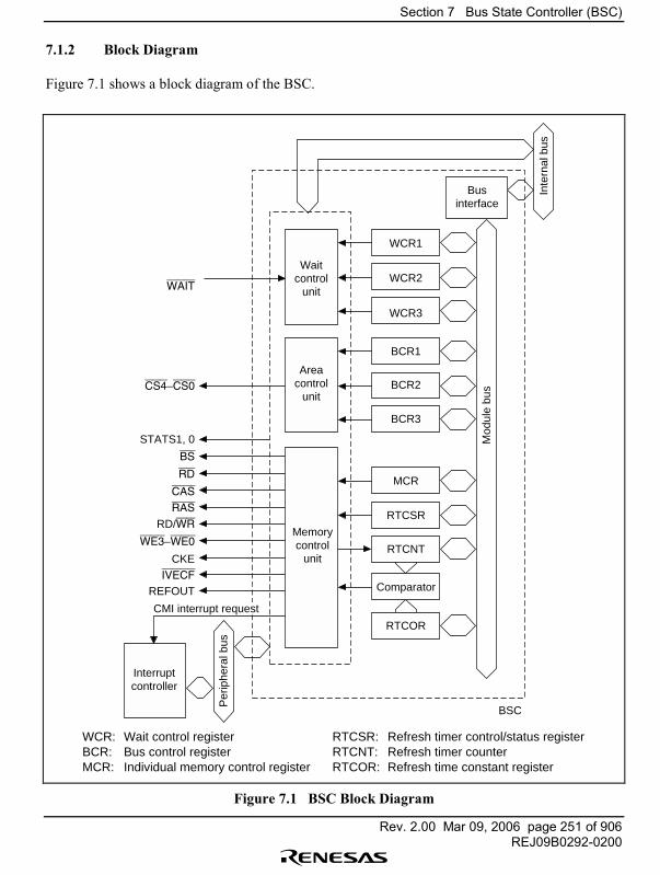
Section 7 Bus State Controller (BSC)
Rev. 2.00 Mar 09, 2006 page 251 of 906REJ09B0292-0200
7.1.2 Block Diagram
Figure 7.1 shows a block diagram of the BSC.
Areacontrol
unit
MCR
BSC
RTCSR
RTCNT
RTCOR
Comparator
Memorycontrol
unit
WCR1
WCR2
WCR3
Waitcontrol
unitWAIT
CS4–CS0
BS
STATS1, 0
RD
CAS
RAS
RD/WR
WE3–WE0
CKE
REFOUTIVECF
Interruptcontroller
Per
iphe
ral b
us
Mod
ule
bus
Inte
rnal
bus
Businterface
WCR: Wait control register RTCSR: Refresh timer control/status registerBCR: Bus control register RTCNT: Refresh timer counterMCR: Individual memory control register RTCOR: Refresh time constant register
CMI interrupt request
BCR1
BCR2
BCR3
Figure 7.1 BSC Block Diagram

Section 7 Bus State Controller (BSC)
Rev. 2.00 Mar 09, 2006 page 252 of 906REJ09B0292-0200
7.1.3 Pin Configuration
Table 7.1 shows the BSC pin configuration.
Table 7.1 Pin Configuration
Signal I/OWith BusReleased Description
A24�A0 O Hi-Z Address bus. 32 Mbytes of memory space can be specified with 25bits
D31�D0 I/O Hi-Z 32-bit data bus. When reading or writing a 16-bit width area, useD15�D0; when reading or writing a 8-bit width area, use D7�D0.With 8-bit accesses that read or write a 32-bit width area, input andoutput the data via the byte position determined by the loweraddress bits of the 32-bit bus
BS O Hi-Z Indicates start of bus cycle or monitor. With the basic interface(device interfaces except for DRAM, synchronous DRAM), signal isasserted for a single clock cycle simultaneous with address output.The start of the bus cycle can be determined by this signal
CS0�CS4 O Hi-Z Chip select. CS3 is not asserted when the CS3 space is DRAMspace
RD/WR O Hi-Z Read/write signal. Signal that indicates access cycle direction(read/write). Connected to WE pin when DRAM/synchronousDRAM is connected
RAS O Hi-Z RAS pin for DRAM/synchronous DRAMCAS/OE O Hi-Z Open when using DRAM
Connected to OE pin when using EDO RAMConnected to CAS pin when using synchronous DRAM
RD O Hi-Z Read pulse signal (read data output enable signal). Normally,connected to the device�s OE pin; when there is an external databuffer, the read cycle data can only be output when this signal islow
WAIT I Don�t care Hardware wait inputBRLS I I Bus release request inputBGR O O Bus grant outputCKE O O Synchronous DRAM clock enable control. Signal for supporting
synchronous DRAM self-refreshIVECF O O Interrupt vector fetchDREQ0 I I DMA request 0DACK0 O O DMA acknowledge 0
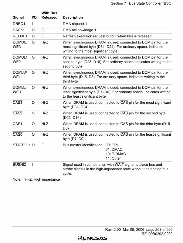
Section 7 Bus State Controller (BSC)
Rev. 2.00 Mar 09, 2006 page 253 of 906REJ09B0292-0200
Signal I/OWith BusReleased Description
DREQ1 I I DMA request 1
DACK1 O O DMA acknowledge 1
REFOUT O O Refresh execution request output when bus is released
DQMUU/WE3
O Hi-Z When synchronous DRAM is used, connected to DQM pin for themost significant byte (D31�D24). For ordinary space, indicateswriting to the most significant byte
DQMUL/WE2
O Hi-Z When synchronous DRAM is used, connected to DQM pin for thesecond byte (D23�D16). For ordinary space, indicates writing to thesecond byte
DQMLU/WE1
O Hi-Z When synchronous DRAM is used, connected to DQM pin for thethird byte (D15�D8). For ordinary space, indicates writing to thethird byte
DQMLL/WE0
O Hi-Z When synchronous DRAM is used, connected to DQM pin for theleast significant byte (D7�D0). For ordinary space, indicates writingto the least significant byte
CAS3 O Hi-Z When DRAM is used, connected to CAS pin for the most significantbyte (D31�D24)
CAS2 O Hi-Z When DRAM is used, connected to CAS pin for the second byte(D23�D16)
CAS1 O Hi-Z When DRAM is used, connected to CAS pin for the third byte (D15�D8)
CAS0 O Hi-Z When DRAM is used, connected to CAS pin for the least significantbyte (D7�D0)
STATS0, 1 O O Bus master identification 00: CPU01: DMAC10: E-DMAC11: Other
BUSHIZ I I Signal used in combination with WAIT signal to place bus andstrobe signals in the high-impedance state without the ending buscycle.
Note: Hi-Z: High impedance
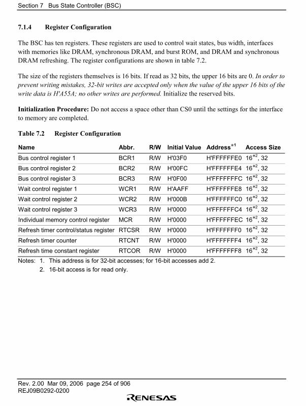
Section 7 Bus State Controller (BSC)
Rev. 2.00 Mar 09, 2006 page 254 of 906REJ09B0292-0200
7.1.4 Register Configuration
The BSC has ten registers. These registers are used to control wait states, bus width, interfaceswith memories like DRAM, synchronous DRAM, and burst ROM, and DRAM and synchronousDRAM refreshing. The register configurations are shown in table 7.2.
The size of the registers themselves is 16 bits. If read as 32 bits, the upper 16 bits are 0. In order toprevent writing mistakes, 32-bit writes are accepted only when the value of the upper 16 bits of thewrite data is H'A55A; no other writes are performed. Initialize the reserved bits.
Initialization Procedure: Do not access a space other than CS0 until the settings for the interfaceto memory are completed.
Table 7.2 Register Configuration
Name Abbr. R/W Initial Value Address*1 Access Size
Bus control register 1 BCR1 R/W H'03F0 H'FFFFFFE0 16*2, 32
Bus control register 2 BCR2 R/W H'00FC H'FFFFFFE4 16*2, 32
Bus control register 3 BCR3 R/W H'0F00 H'FFFFFFFC 16*2, 32
Wait control register 1 WCR1 R/W H'AAFF H'FFFFFFE8 16*2, 32
Wait control register 2 WCR2 R/W H'000B H'FFFFFFC0 16*2, 32
Wait control register 3 WCR3 R/W H'0000 H'FFFFFFC4 16*2, 32
Individual memory control register MCR R/W H'0000 H'FFFFFFEC 16*2, 32
Refresh timer control/status register RTCSR R/W H'0000 H'FFFFFFF0 16*2, 32
Refresh timer counter RTCNT R/W H'0000 H'FFFFFFF4 16*2, 32
Refresh time constant register RTCOR R/W H'0000 H'FFFFFFF8 16*2, 32Notes: 1. This address is for 32-bit accesses; for 16-bit accesses add 2.
2. 16-bit access is for read only.
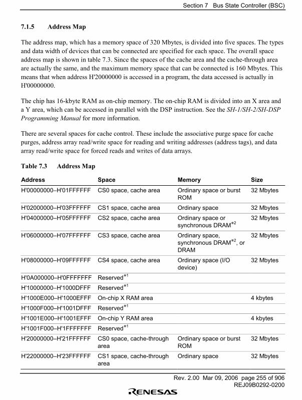
Section 7 Bus State Controller (BSC)
Rev. 2.00 Mar 09, 2006 page 255 of 906REJ09B0292-0200
7.1.5 Address Map
The address map, which has a memory space of 320 Mbytes, is divided into five spaces. The typesand data width of devices that can be connected are specified for each space. The overall spaceaddress map is shown in table 7.3. Since the spaces of the cache area and the cache-through areaare actually the same, and the maximum memory space that can be connected is 160 Mbytes. Thismeans that when address H'20000000 is accessed in a program, the data accessed is actually inH'00000000.
The chip has 16-kbyte RAM as on-chip memory. The on-chip RAM is divided into an X area anda Y area, which can be accessed in parallel with the DSP instruction. See the SH-1/SH-2/SH-DSPProgramming Manual for more information.
There are several spaces for cache control. These include the associative purge space for cachepurges, address array read/write space for reading and writing addresses (address tags), and dataarray read/write space for forced reads and writes of data arrays.
Table 7.3 Address Map
Address Space Memory Size
H'00000000�H'01FFFFFF CS0 space, cache area Ordinary space or burstROM
32 Mbytes
H'02000000�H'03FFFFFF CS1 space, cache area Ordinary space 32 Mbytes
H'04000000�H'05FFFFFF CS2 space, cache area Ordinary space orsynchronous DRAM*2
32 Mbytes
H'06000000�H'07FFFFFF CS3 space, cache area Ordinary space,synchronous DRAM*2, orDRAM
32 Mbytes
H'08000000�H'09FFFFFF CS4 space, cache area Ordinary space (I/Odevice)
32 Mbytes
H'0A000000�H'0FFFFFFF Reserved*1
H'10000000�H'1000DFFF Reserved*1
H'1000E000�H'1000EFFF On-chip X RAM area 4 kbytes
H'1000F000�H'1001DFFF Reserved*1
H'1001E000�H'1001EFFF On-chip Y RAM area 4 kbytes
H'1001F000�H'1FFFFFFF Reserved*1
H'20000000�H'21FFFFFF CS0 space, cache-througharea
Ordinary space or burstROM
32 Mbytes
H'22000000�H'23FFFFFF CS1 space, cache-througharea
Ordinary space 32 Mbytes
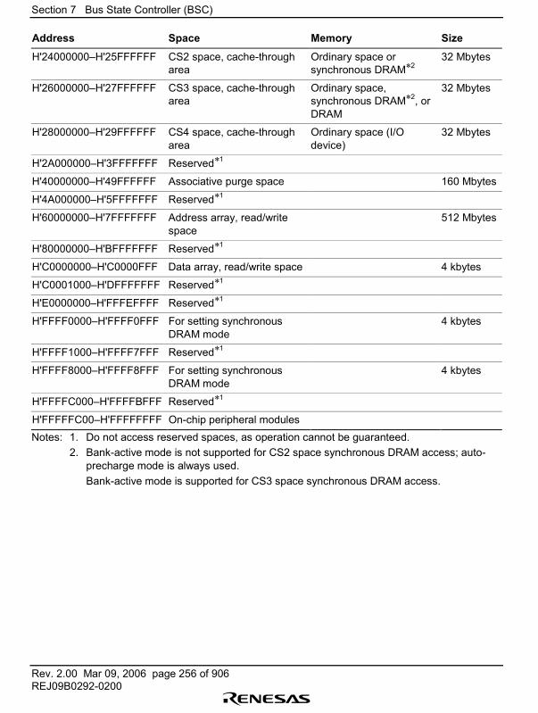
Section 7 Bus State Controller (BSC)
Rev. 2.00 Mar 09, 2006 page 256 of 906REJ09B0292-0200
Address Space Memory Size
H'24000000�H'25FFFFFF CS2 space, cache-througharea
Ordinary space orsynchronous DRAM*2
32 Mbytes
H'26000000�H'27FFFFFF CS3 space, cache-througharea
Ordinary space,synchronous DRAM*2, orDRAM
32 Mbytes
H'28000000�H'29FFFFFF CS4 space, cache-througharea
Ordinary space (I/Odevice)
32 Mbytes
H'2A000000�H'3FFFFFFF Reserved*1
H'40000000�H'49FFFFFF Associative purge space 160 Mbytes
H'4A000000�H'5FFFFFFF Reserved*1
H'60000000�H'7FFFFFFF Address array, read/writespace
512 Mbytes
H'80000000�H'BFFFFFFF Reserved*1
H'C0000000�H'C0000FFF Data array, read/write space 4 kbytes
H'C0001000�H'DFFFFFFF Reserved*1
H'E0000000�H'FFFEFFFF Reserved*1
H'FFFF0000�H'FFFF0FFF For setting synchronousDRAM mode
4 kbytes
H'FFFF1000�H'FFFF7FFF Reserved*1
H'FFFF8000�H'FFFF8FFF For setting synchronousDRAM mode
4 kbytes
H'FFFFC000�H'FFFFBFFF Reserved*1
H'FFFFFC00�H'FFFFFFFF On-chip peripheral modulesNotes: 1. Do not access reserved spaces, as operation cannot be guaranteed.
2. Bank-active mode is not supported for CS2 space synchronous DRAM access; auto-precharge mode is always used.Bank-active mode is supported for CS3 space synchronous DRAM access.
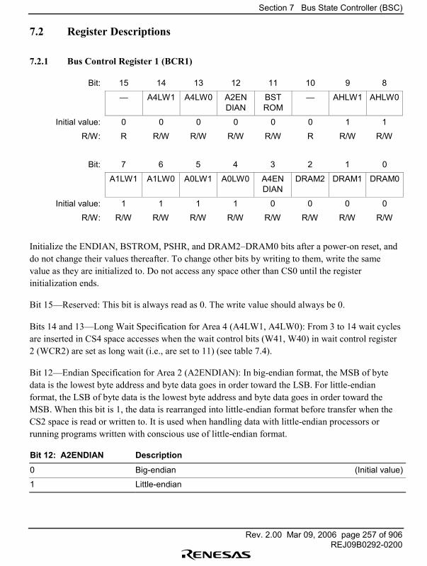
Section 7 Bus State Controller (BSC)
Rev. 2.00 Mar 09, 2006 page 257 of 906REJ09B0292-0200
7.2 Register Descriptions
7.2.1 Bus Control Register 1 (BCR1)
Bit: 15 14 13 12 11 10 9 8
� A4LW1 A4LW0 A2ENDIAN
BSTROM
� AHLW1 AHLW0
Initial value: 0 0 0 0 0 0 1 1
R/W: R R/W R/W R/W R/W R R/W R/W
Bit: 7 6 5 4 3 2 1 0
A1LW1 A1LW0 A0LW1 A0LW0 A4ENDIAN
DRAM2 DRAM1 DRAM0
Initial value: 1 1 1 1 0 0 0 0
R/W: R/W R/W R/W R/W R/W R/W R/W R/W
Initialize the ENDIAN, BSTROM, PSHR, and DRAM2�DRAM0 bits after a power-on reset, anddo not change their values thereafter. To change other bits by writing to them, write the samevalue as they are initialized to. Do not access any space other than CS0 until the registerinitialization ends.
Bit 15�Reserved: This bit is always read as 0. The write value should always be 0.
Bits 14 and 13�Long Wait Specification for Area 4 (A4LW1, A4LW0): From 3 to 14 wait cyclesare inserted in CS4 space accesses when the wait control bits (W41, W40) in wait control register2 (WCR2) are set as long wait (i.e., are set to 11) (see table 7.4).
Bit 12�Endian Specification for Area 2 (A2ENDIAN): In big-endian format, the MSB of bytedata is the lowest byte address and byte data goes in order toward the LSB. For little-endianformat, the LSB of byte data is the lowest byte address and byte data goes in order toward theMSB. When this bit is 1, the data is rearranged into little-endian format before transfer when theCS2 space is read or written to. It is used when handling data with little-endian processors orrunning programs written with conscious use of little-endian format.
Bit 12: A2ENDIAN Description
0 Big-endian (Initial value)
1 Little-endian
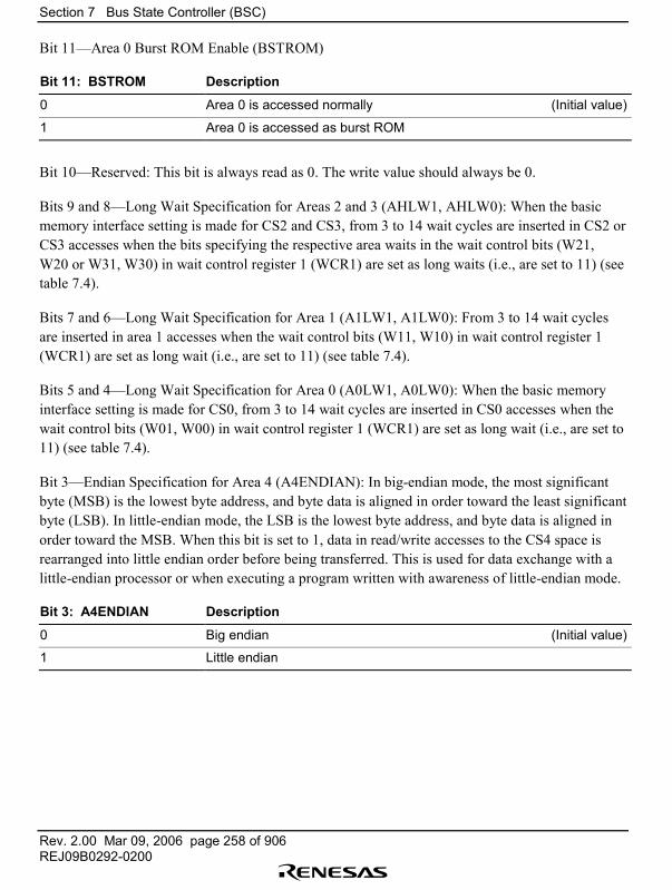
Section 7 Bus State Controller (BSC)
Rev. 2.00 Mar 09, 2006 page 258 of 906REJ09B0292-0200
Bit 11�Area 0 Burst ROM Enable (BSTROM)
Bit 11: BSTROM Description
0 Area 0 is accessed normally (Initial value)
1 Area 0 is accessed as burst ROM
Bit 10�Reserved: This bit is always read as 0. The write value should always be 0.
Bits 9 and 8�Long Wait Specification for Areas 2 and 3 (AHLW1, AHLW0): When the basicmemory interface setting is made for CS2 and CS3, from 3 to 14 wait cycles are inserted in CS2 orCS3 accesses when the bits specifying the respective area waits in the wait control bits (W21,W20 or W31, W30) in wait control register 1 (WCR1) are set as long waits (i.e., are set to 11) (seetable 7.4).
Bits 7 and 6�Long Wait Specification for Area 1 (A1LW1, A1LW0): From 3 to 14 wait cyclesare inserted in area 1 accesses when the wait control bits (W11, W10) in wait control register 1(WCR1) are set as long wait (i.e., are set to 11) (see table 7.4).
Bits 5 and 4�Long Wait Specification for Area 0 (A0LW1, A0LW0): When the basic memoryinterface setting is made for CS0, from 3 to 14 wait cycles are inserted in CS0 accesses when thewait control bits (W01, W00) in wait control register 1 (WCR1) are set as long wait (i.e., are set to11) (see table 7.4).
Bit 3�Endian Specification for Area 4 (A4ENDIAN): In big-endian mode, the most significantbyte (MSB) is the lowest byte address, and byte data is aligned in order toward the least significantbyte (LSB). In little-endian mode, the LSB is the lowest byte address, and byte data is aligned inorder toward the MSB. When this bit is set to 1, data in read/write accesses to the CS4 space isrearranged into little endian order before being transferred. This is used for data exchange with alittle-endian processor or when executing a program written with awareness of little-endian mode.
Bit 3: A4ENDIAN Description
0 Big endian (Initial value)
1 Little endian
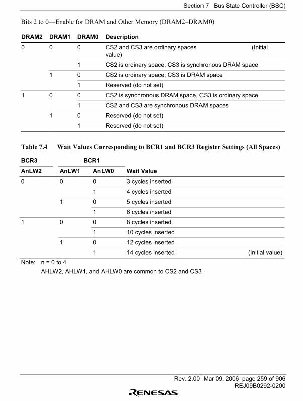
Section 7 Bus State Controller (BSC)
Rev. 2.00 Mar 09, 2006 page 259 of 906REJ09B0292-0200
Bits 2 to 0�Enable for DRAM and Other Memory (DRAM2�DRAM0)
DRAM2 DRAM1 DRAM0 Description
0 0 0 CS2 and CS3 are ordinary spaces (Initialvalue)
1 CS2 is ordinary space; CS3 is synchronous DRAM space
1 0 CS2 is ordinary space; CS3 is DRAM space
1 Reserved (do not set)
1 0 0 CS2 is synchronous DRAM space, CS3 is ordinary space
1 CS2 and CS3 are synchronous DRAM spaces
1 0 Reserved (do not set)
1 Reserved (do not set)
Table 7.4 Wait Values Corresponding to BCR1 and BCR3 Register Settings (All Spaces)
BCR3 BCR1
AnLW2 AnLW1 AnLW0 Wait Value
0 0 0 3 cycles inserted
1 4 cycles inserted
1 0 5 cycles inserted
1 6 cycles inserted
1 0 0 8 cycles inserted
1 10 cycles inserted
1 0 12 cycles inserted
1 14 cycles inserted (Initial value)Note: n = 0 to 4
AHLW2, AHLW1, and AHLW0 are common to CS2 and CS3.
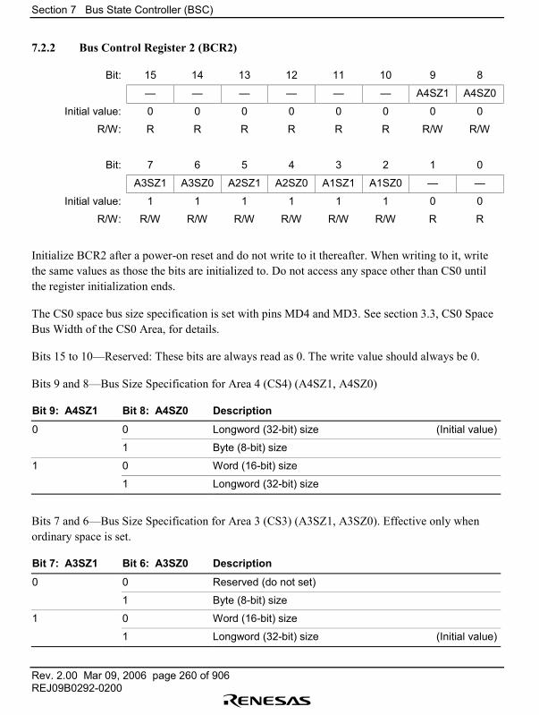
Section 7 Bus State Controller (BSC)
Rev. 2.00 Mar 09, 2006 page 260 of 906REJ09B0292-0200
7.2.2 Bus Control Register 2 (BCR2)
Bit: 15 14 13 12 11 10 9 8
� � � � � � A4SZ1 A4SZ0
Initial value: 0 0 0 0 0 0 0 0
R/W: R R R R R R R/W R/W
Bit: 7 6 5 4 3 2 1 0
A3SZ1 A3SZ0 A2SZ1 A2SZ0 A1SZ1 A1SZ0 � �
Initial value: 1 1 1 1 1 1 0 0
R/W: R/W R/W R/W R/W R/W R/W R R
Initialize BCR2 after a power-on reset and do not write to it thereafter. When writing to it, writethe same values as those the bits are initialized to. Do not access any space other than CS0 untilthe register initialization ends.
The CS0 space bus size specification is set with pins MD4 and MD3. See section 3.3, CS0 SpaceBus Width of the CS0 Area, for details.
Bits 15 to 10�Reserved: These bits are always read as 0. The write value should always be 0.
Bits 9 and 8�Bus Size Specification for Area 4 (CS4) (A4SZ1, A4SZ0)
Bit 9: A4SZ1 Bit 8: A4SZ0 Description
0 0 Longword (32-bit) size (Initial value)
1 Byte (8-bit) size
1 0 Word (16-bit) size
1 Longword (32-bit) size
Bits 7 and 6�Bus Size Specification for Area 3 (CS3) (A3SZ1, A3SZ0). Effective only whenordinary space is set.
Bit 7: A3SZ1 Bit 6: A3SZ0 Description
0 0 Reserved (do not set)
1 Byte (8-bit) size
1 0 Word (16-bit) size
1 Longword (32-bit) size (Initial value)
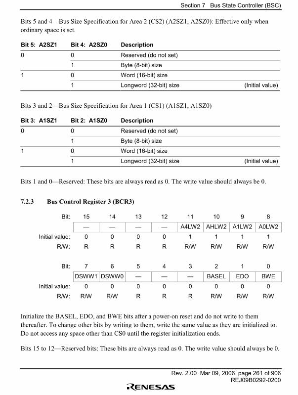
Section 7 Bus State Controller (BSC)
Rev. 2.00 Mar 09, 2006 page 261 of 906REJ09B0292-0200
Bits 5 and 4�Bus Size Specification for Area 2 (CS2) (A2SZ1, A2SZ0): Effective only whenordinary space is set.
Bit 5: A2SZ1 Bit 4: A2SZ0 Description
0 0 Reserved (do not set)
1 Byte (8-bit) size
1 0 Word (16-bit) size
1 Longword (32-bit) size (Initial value)
Bits 3 and 2�Bus Size Specification for Area 1 (CS1) (A1SZ1, A1SZ0)
Bit 3: A1SZ1 Bit 2: A1SZ0 Description
0 0 Reserved (do not set)
1 Byte (8-bit) size
1 0 Word (16-bit) size
1 Longword (32-bit) size (Initial value)
Bits 1 and 0�Reserved: These bits are always read as 0. The write value should always be 0.
7.2.3 Bus Control Register 3 (BCR3)
Bit: 15 14 13 12 11 10 9 8
� � � � A4LW2 AHLW2 A1LW2 A0LW2
Initial value: 0 0 0 0 1 1 1 1
R/W: R R R R R/W R/W R/W R/W
Bit: 7 6 5 4 3 2 1 0
DSWW1 DSWW0 � � � BASEL EDO BWE
Initial value: 0 0 0 0 0 0 0 0
R/W: R/W R/W R R R R/W R/W R/W
Initialize the BASEL, EDO, and BWE bits after a power-on reset and do not write to themthereafter. To change other bits by writing to them, write the same value as they are initialized to.Do not access any space other than CS0 until the register initialization ends.
Bits 15 to 12�Reserved bits: These bits are always read as 0. The write value should always be 0.
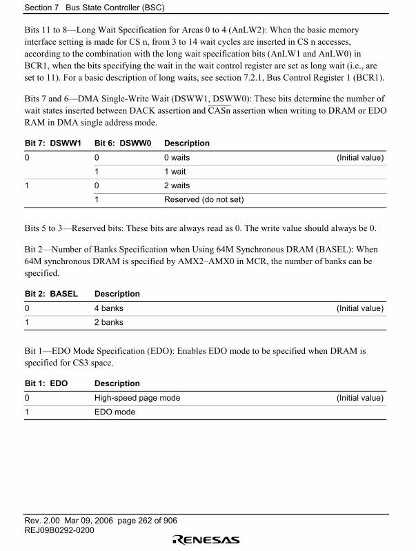
Section 7 Bus State Controller (BSC)
Rev. 2.00 Mar 09, 2006 page 262 of 906REJ09B0292-0200
Bits 11 to 8�Long Wait Specification for Areas 0 to 4 (AnLW2): When the basic memoryinterface setting is made for CS n, from 3 to 14 wait cycles are inserted in CS n accesses,according to the combination with the long wait specification bits (AnLW1 and AnLW0) inBCR1, when the bits specifying the wait in the wait control register are set as long wait (i.e., areset to 11). For a basic description of long waits, see section 7.2.1, Bus Control Register 1 (BCR1).
Bits 7 and 6�DMA Single-Write Wait (DSWW1, DSWW0): These bits determine the number ofwait states inserted between DACK assertion and CASn assertion when writing to DRAM or EDORAM in DMA single address mode.
Bit 7: DSWW1 Bit 6: DSWW0 Description
0 0 0 waits (Initial value)
1 1 wait
1 0 2 waits
1 Reserved (do not set)
Bits 5 to 3�Reserved bits: These bits are always read as 0. The write value should always be 0.
Bit 2�Number of Banks Specification when Using 64M Synchronous DRAM (BASEL): When64M synchronous DRAM is specified by AMX2�AMX0 in MCR, the number of banks can bespecified.
Bit 2: BASEL Description
0 4 banks (Initial value)
1 2 banks
Bit 1�EDO Mode Specification (EDO): Enables EDO mode to be specified when DRAM isspecified for CS3 space.
Bit 1: EDO Description
0 High-speed page mode (Initial value)
1 EDO mode
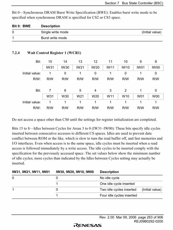
Section 7 Bus State Controller (BSC)
Rev. 2.00 Mar 09, 2006 page 263 of 906REJ09B0292-0200
Bit 0�Synchronous DRAM Burst Write Specification (BWE): Enables burst write mode to bespecified when synchronous DRAM is specified for CS2 or CS3 space.
Bit 0: BWE Description
0 Single write mode (Initial value)
1 Burst write mode
7.2.4 Wait Control Register 1 (WCR1)
Bit: 15 14 13 12 11 10 9 8
IW31 IW30 IW21 IW20 IW11 IW10 IW01 IW00
Initial value: 1 0 1 0 1 0 1 0
R/W: R/W R/W R/W R/W R/W R/W R/W R/W
Bit: 7 6 5 4 3 2 1 0
W31 W30 W21 W20 W11 W10 W01 W00
Initial value: 1 1 1 1 1 1 1 1
R/W: R/W R/W R/W R/W R/W R/W R/W R/W
Do not access a space other than CS0 until the settings for register initialization are completed.
Bits 15 to 8�Idles between Cycles for Areas 3 to 0 (IW31�IW00): These bits specify idle cyclesinserted between consecutive accesses to different CS spaces. Idles are used to prevent dataconflict between ROM or the like, which is slow to turn the read buffer off, and fast memories andI/O interfaces. Even when access is to the same space, idle cycles must be inserted when a readaccess is followed immediately by a write access. The idle cycles to be inserted comply with thespecification for the previously accessed space. The set values below show the minimum numberof idle cycles; more cycles than indicated by the Idles between Cycles setting may actually beinserted.
IW31, IW21, IW11, IW01 IW30, IW20, IW10, IW00 Description
0 0 No idle cycle
1 One idle cycle inserted
1 0 Two idle cycles inserted (Initial value)
1 Four idle cycles inserted
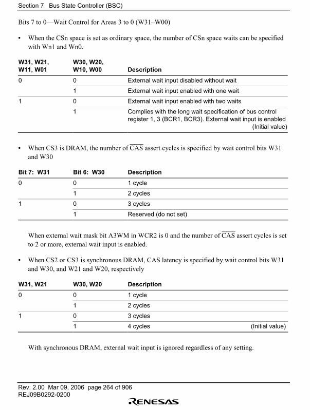
Section 7 Bus State Controller (BSC)
Rev. 2.00 Mar 09, 2006 page 264 of 906REJ09B0292-0200
Bits 7 to 0�Wait Control for Areas 3 to 0 (W31�W00)
• When the CSn space is set as ordinary space, the number of CSn space waits can be specifiedwith Wn1 and Wn0.
W31, W21,W11, W01
W30, W20,W10, W00 Description
0 0 External wait input disabled without wait
1 External wait input enabled with one wait
1 0 External wait input enabled with two waits
1 Complies with the long wait specification of bus controlregister 1, 3 (BCR1, BCR3). External wait input is enabled
(Initial value)
• When CS3 is DRAM, the number of CAS assert cycles is specified by wait control bits W31and W30
Bit 7: W31 Bit 6: W30 Description
0 0 1 cycle
1 2 cycles
1 0 3 cycles
1 Reserved (do not set)
When external wait mask bit A3WM in WCR2 is 0 and the number of CAS assert cycles is setto 2 or more, external wait input is enabled.
• When CS2 or CS3 is synchronous DRAM, CAS latency is specified by wait control bits W31and W30, and W21 and W20, respectively
W31, W21 W30, W20 Description
0 0 1 cycle
1 2 cycles
1 0 3 cycles
1 4 cycles (Initial value)
With synchronous DRAM, external wait input is ignored regardless of any setting.

Section 7 Bus State Controller (BSC)
Rev. 2.00 Mar 09, 2006 page 265 of 906REJ09B0292-0200
7.2.5 Wait Control Register 2 (WCR2)
Bit: 15 14 13 12 11 10 9 8
A4WD1 A4WD0 � A4WM A3WM A2WM A1WM A0WM
Initial value: 0 0 0 0 0 0 0 0
R/W: R/W R/W R R/W R/W R/W R/W R/W
Bit: 7 6 5 4 3 2 1 0
� � � � IW41 IW40 W41 W40
Initial value: 0 0 0 0 1 0 1 1
R/W: R R R R R/W R/W R/W R/W
Bits 15 and 14�Number of External Waits Specification for Area 4 (A4WD1, A4WD0): Thesebits specify the number of cycles between acceptance of CS4 space external wait negation and RDor WEn negation.
Bit 15: A4WD1 Bit 14: A4WD0 Description
0 0 1 cycle (Initial value)
1 2 cycles
1 0 4 cycles
1 Reserved (do not set)
Bit 13�Reserved bit. This bit is always read as 0. The write value should always be 0.
Bits 12 to 8�External Wait Mask Specification for Areas 0 to 4 (A4WM�A0WM): These bitsenable waits to be masked for CS spaces 0 to 4. When a value other than 00 is set in the waitcontrol bits for CS spaces 0 to 4 (W41�W00), external wait input can be enabled, but the waitinput can be masked by setting these bits to 1. With synchronous DRAM, external wait input isignored regardless of the settings.
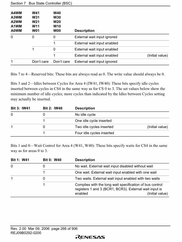
Section 7 Bus State Controller (BSC)
Rev. 2.00 Mar 09, 2006 page 266 of 906REJ09B0292-0200
A4WMA3WMA2WMA1WMA0WM
W41W31W21W11W01
W40W30W20W10W00 Description
0 0 0 External wait input ignored
1 External wait input enabled
1 0 External wait input enabled
1 External wait input enabled (Initial value)
1 Don�t care Don�t care External wait input ignored
Bits 7 to 4�Reserved bits: These bits are always read as 0. The write value should always be 0.
Bits 3 and 2�Idles between Cycles for Area 4 (IW41, IW40): These bits specify idle cyclesinserted between cycles in CS4 in the same way as for CS 0 to 3. The set values below show theminimum number of idle cycles; more cycles than indicated by the Idles between Cycles settingmay actually be inserted.
Bit 3: IW41 Bit 2: IW40 Description
0 0 No idle cycle
1 One idle cycle inserted
1 0 Two idle cycles inserted (Initial value)
1 Four idle cycles inserted
Bits 1 and 0�Wait Control for Area 4 (W41, W40): These bits specify waits for CS4 in the sameway as for areas 0 to 3.
Bit 1: W41 Bit 0: W40 Description
0 0 No wait. External wait input disabled without wait
1 One wait. External wait input enabled with one wait
1 0 Two waits. External wait input enabled with two waits
1 Complies with the long wait specification of bus controlregisters 1 and 3 (BCR1, BCR3). External wait input isenabled (Initial value)
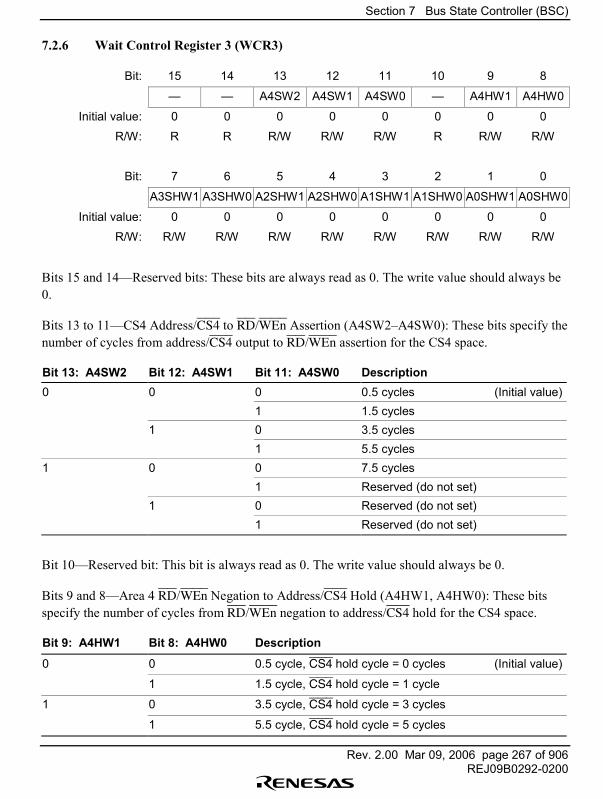
Section 7 Bus State Controller (BSC)
Rev. 2.00 Mar 09, 2006 page 267 of 906REJ09B0292-0200
7.2.6 Wait Control Register 3 (WCR3)
Bit: 15 14 13 12 11 10 9 8
� � A4SW2 A4SW1 A4SW0 � A4HW1 A4HW0
Initial value: 0 0 0 0 0 0 0 0
R/W: R R R/W R/W R/W R R/W R/W
Bit: 7 6 5 4 3 2 1 0
A3SHW1 A3SHW0 A2SHW1 A2SHW0 A1SHW1 A1SHW0 A0SHW1 A0SHW0
Initial value: 0 0 0 0 0 0 0 0
R/W: R/W R/W R/W R/W R/W R/W R/W R/W
Bits 15 and 14�Reserved bits: These bits are always read as 0. The write value should always be0.
Bits 13 to 11�CS4 Address/CS4 to RD/WEn Assertion (A4SW2�A4SW0): These bits specify thenumber of cycles from address/CS4 output to RD/WEn assertion for the CS4 space.
Bit 13: A4SW2 Bit 12: A4SW1 Bit 11: A4SW0 Description0 0 0 0.5 cycles (Initial value)
1 1.5 cycles1 0 3.5 cycles
1 5.5 cycles1 0 0 7.5 cycles
1 Reserved (do not set)1 0 Reserved (do not set)
1 Reserved (do not set)
Bit 10�Reserved bit: This bit is always read as 0. The write value should always be 0.
Bits 9 and 8�Area 4 RD/WEn Negation to Address/CS4 Hold (A4HW1, A4HW0): These bitsspecify the number of cycles from RD/WEn negation to address/CS4 hold for the CS4 space.
Bit 9: A4HW1 Bit 8: A4HW0 Description
0 0 0.5 cycle, CS4 hold cycle = 0 cycles (Initial value)
1 1.5 cycle, CS4 hold cycle = 1 cycle
1 0 3.5 cycle, CS4 hold cycle = 3 cycles
1 5.5 cycle, CS4 hold cycle = 5 cycles
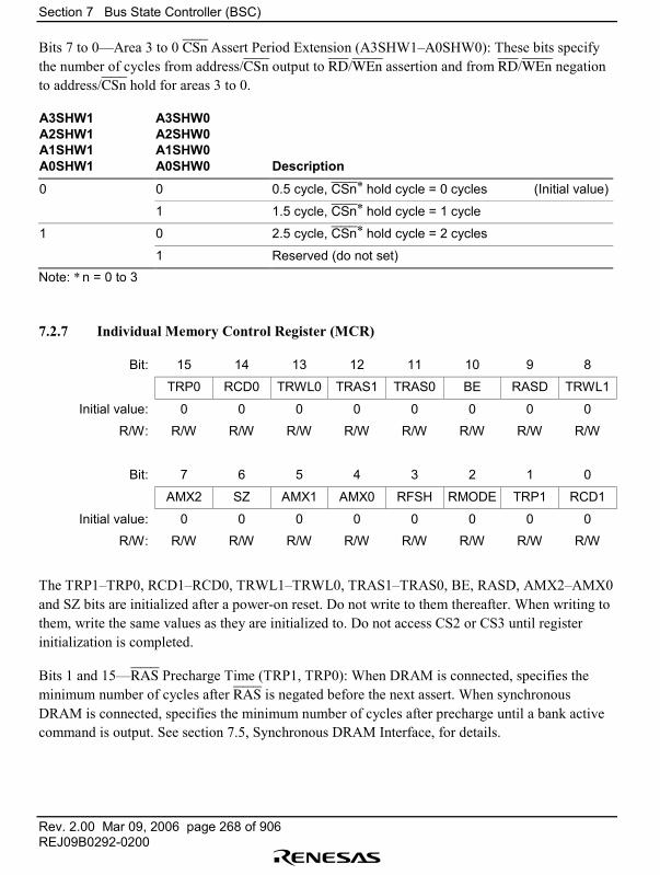
Section 7 Bus State Controller (BSC)
Rev. 2.00 Mar 09, 2006 page 268 of 906REJ09B0292-0200
Bits 7 to 0�Area 3 to 0 CSn Assert Period Extension (A3SHW1�A0SHW0): These bits specifythe number of cycles from address/CSn output to RD/WEn assertion and from RD/WEn negationto address/CSn hold for areas 3 to 0.
A3SHW1A2SHW1A1SHW1A0SHW1
A3SHW0A2SHW0A1SHW0A0SHW0 Description
0 0 0.5 cycle, CSn* hold cycle = 0 cycles (Initial value)
1 1.5 cycle, CSn* hold cycle = 1 cycle
1 0 2.5 cycle, CSn* hold cycle = 2 cycles
1 Reserved (do not set)Note: * n = 0 to 3
7.2.7 Individual Memory Control Register (MCR)
Bit: 15 14 13 12 11 10 9 8
TRP0 RCD0 TRWL0 TRAS1 TRAS0 BE RASD TRWL1
Initial value: 0 0 0 0 0 0 0 0
R/W: R/W R/W R/W R/W R/W R/W R/W R/W
Bit: 7 6 5 4 3 2 1 0
AMX2 SZ AMX1 AMX0 RFSH RMODE TRP1 RCD1
Initial value: 0 0 0 0 0 0 0 0
R/W: R/W R/W R/W R/W R/W R/W R/W R/W
The TRP1�TRP0, RCD1�RCD0, TRWL1�TRWL0, TRAS1�TRAS0, BE, RASD, AMX2�AMX0and SZ bits are initialized after a power-on reset. Do not write to them thereafter. When writing tothem, write the same values as they are initialized to. Do not access CS2 or CS3 until registerinitialization is completed.
Bits 1 and 15�RAS Precharge Time (TRP1, TRP0): When DRAM is connected, specifies theminimum number of cycles after RAS is negated before the next assert. When synchronousDRAM is connected, specifies the minimum number of cycles after precharge until a bank activecommand is output. See section 7.5, Synchronous DRAM Interface, for details.
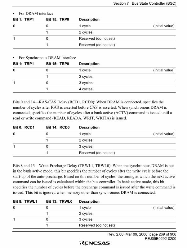
Section 7 Bus State Controller (BSC)
Rev. 2.00 Mar 09, 2006 page 269 of 906REJ09B0292-0200
• For DRAM interfaceBit 1: TRP1 Bit 15: TRP0 Description
0 0 1 cycle (Initial value)
1 2 cycles
1 0 Reserved (do not set)
1 Reserved (do not set)
• For Synchronous DRAM interfaceBit 1: TRP1 Bit 15: TRP0 Description
0 0 1 cycle (Initial value)
1 2 cycles
1 0 3 cycles
1 4 cycles
Bits 0 and 14�RAS-CAS Delay (RCD1, RCD0): When DRAM is connected, specifies thenumber of cycles after RAS is asserted before CAS is asserted. When synchronous DRAM isconnected, specifies the number of cycles after a bank active (ACTV) command is issued until aread or write command (READ, READA, WRIT, WRITA) is issued.
Bit 0: RCD1 Bit 14: RCD0 Description
0 0 1 cycle (Initial value)
1 2 cycles
1 0 3 cycles
1 Reserved (do not set)
Bits 8 and 13�Write-Precharge Delay (TRWL1, TRWL0): When the synchronous DRAM is notin the bank active mode, this bit specifies the number of cycles after the write cycle before thestart-up of the auto-precharge. Based on this number of cycles, the timing at which the next activecommand can be issued is calculated within the bus controller. In bank active mode, this bitspecifies the number of cycles before the precharge command is issued after the write command isissued. This bit is ignored when memory other than synchronous DRAM is connected.
Bit 8: TRWL1 Bit 13: TRWL0 Description0 0 1 cycle (Initial value)
1 2 cycles1 0 3 cycles
1 Reserved (do not set)
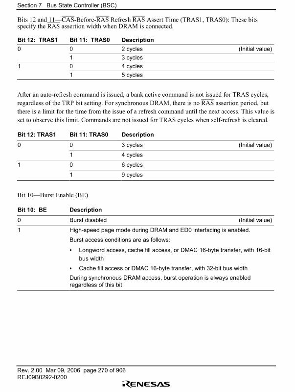
Section 7 Bus State Controller (BSC)
Rev. 2.00 Mar 09, 2006 page 270 of 906REJ09B0292-0200
Bits 12 and 11�CAS-Before-RAS Refresh RAS Assert Time (TRAS1, TRAS0): These bitsspecify the RAS assertion width when DRAM is connected.
Bit 12: TRAS1 Bit 11: TRAS0 Description0 0 2 cycles (Initial value)
1 3 cycles1 0 4 cycles
1 5 cycles
After an auto-refresh command is issued, a bank active command is not issued for TRAS cycles,regardless of the TRP bit setting. For synchronous DRAM, there is no RAS assertion period, butthere is a limit for the time from the issue of a refresh command until the next access. This value isset to observe this limit. Commands are not issued for TRAS cycles when self-refresh is cleared.
Bit 12: TRAS1 Bit 11: TRAS0 Description
0 0 3 cycles (Initial value)
1 4 cycles
1 0 6 cycles
1 9 cycles
Bit 10�Burst Enable (BE)
Bit 10: BE Description
0 Burst disabled (Initial value)
1 High-speed page mode during DRAM and ED0 interfacing is enabled.
Burst access conditions are as follows:
• Longword access, cache fill access, or DMAC 16-byte transfer, with 16-bitbus width
• Cache fill access or DMAC 16-byte transfer, with 32-bit bus widthDuring synchronous DRAM access, burst operation is always enabledregardless of this bit
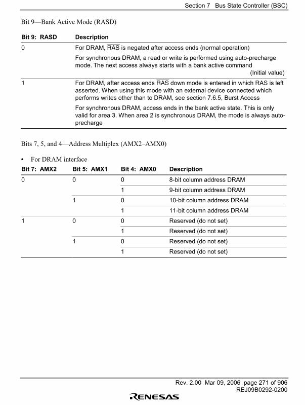
Section 7 Bus State Controller (BSC)
Rev. 2.00 Mar 09, 2006 page 271 of 906REJ09B0292-0200
Bit 9�Bank Active Mode (RASD)
Bit 9: RASD Description
0 For DRAM, RAS is negated after access ends (normal operation)
For synchronous DRAM, a read or write is performed using auto-prechargemode. The next access always starts with a bank active command
(Initial value)
1 For DRAM, after access ends RAS down mode is entered in which RAS is leftasserted. When using this mode with an external device connected whichperforms writes other than to DRAM, see section 7.6.5, Burst Access
For synchronous DRAM, access ends in the bank active state. This is onlyvalid for area 3. When area 2 is synchronous DRAM, the mode is always auto-precharge
Bits 7, 5, and 4�Address Multiplex (AMX2�AMX0)
• For DRAM interfaceBit 7: AMX2 Bit 5: AMX1 Bit 4: AMX0 Description
0 0 0 8-bit column address DRAM
1 9-bit column address DRAM
1 0 10-bit column address DRAM
1 11-bit column address DRAM
1 0 0 Reserved (do not set)
1 Reserved (do not set)
1 0 Reserved (do not set)
1 Reserved (do not set)
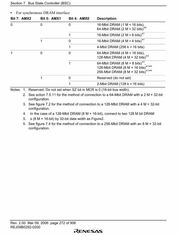
Section 7 Bus State Controller (BSC)
Rev. 2.00 Mar 09, 2006 page 272 of 906REJ09B0292-0200
• For synchronous DRAM interfaceBit 7: AMX2 Bit 5: AMX1 Bit 4: AMX0 Description
0 0 0 16-Mbit DRAM (1 M × 16 bits),64-Mbit DRAM (2 M × 32 bits)*2
1 16-Mbit DRAM (2 M × 8 bits)*1
1 0 16-Mbit DRAM (4 M × 4 bits)*1
1 4-Mbit DRAM (256 k × 16 bits)
1 0 0 64-Mbit DRAM (4 M × 16 bits),128-Mbit DRAM (4 M × 32 bits)*3
1 64-Mbit DRAM (8 M × 8 bits)*1,128-Mbit DRAM (8 M × 16 bits)*1*4
256-Mbit DRAM (8 M × 32 bits)*1*4
1 0 Reserved (do not set)
1 2-Mbit DRAM (128 k × 16 bits)Notes: 1. Reserved. Do not set when SZ bit in MCR is 0 (16-bit bus width).
2. See sction 7.5.11 for the method of connection to a 64-Mbit DRAM with a 2 M × 32-bitconfiguration.
3. See figure 7.2 for the method of connection to a 128-Mbit DRAM with a 4 M × 32-bitconfiguration.
4. In the case of a 128-Mbit DRAM (8 M × 16-bit), connect to two 128 M bit DRAM5. s (8 M × 16-bit) by 32-bit data width as Figure2.5. See figure 7.4 for the method of connection to a 256-Mbit DRAM with an 8 M × 32-bit
configuration.
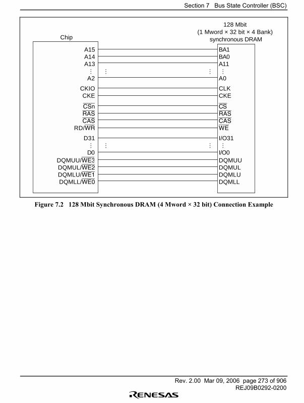
Section 7 Bus State Controller (BSC)
Rev. 2.00 Mar 09, 2006 page 273 of 906REJ09B0292-0200
A15 BA1A14 BA0A13 A11
A2 A0
CKIO CLKCKE CKE
CSn CS
RAS RAS
CAS CAS
RD/WR WE
D31 I/O31
D0 I/O0DQMUU/WE3 DQMUUDQMUL/WE2 DQMULDQMLU/WE1 DQMLUDQMLL/WE0 DQMLL
128 Mbit (1 Mword × 32 bit × 4 Bank)
synchronous DRAMChip
… … … …
… … … …
Figure 7.2 128 Mbit Synchronous DRAM (4 Mword × 32 bit) Connection Example
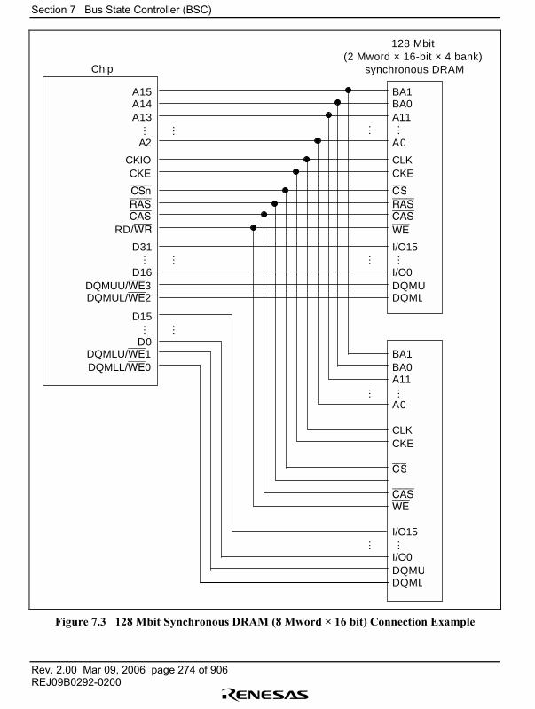
Section 7 Bus State Controller (BSC)
Rev. 2.00 Mar 09, 2006 page 274 of 906REJ09B0292-0200
A15 BA1A14 BA0A13 A11
A2 A0
CKIO CLKCKE CKE
CSn CS
RAS RASCAS CAS
RD/WR
D31 I/O15
D16 I/O0DQMUU/WE3 DQMUDQMUL/WE2 DQML
D15
D0DQMLU/WE1 BA1DQMLL/WE0 BA0
A11
A0
CLKCKE
CS
CASWE
I/O15
I/O0DQMUDQML
WE
Chip
128 Mbit (2 Mword × 16-bit × 4 bank)
synchronous DRAM
……
…………
……
……
……
……
Figure 7.3 128 Mbit Synchronous DRAM (8 Mword × 16 bit) Connection Example
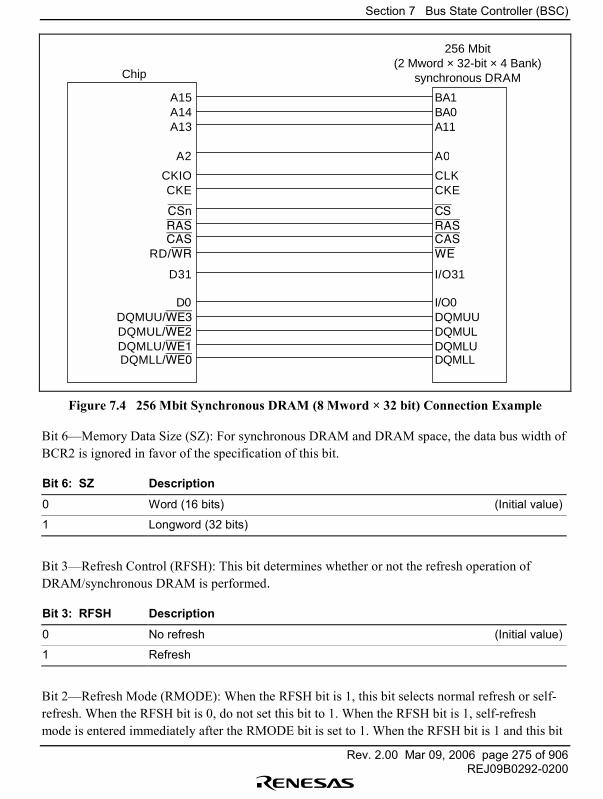
Section 7 Bus State Controller (BSC)
Rev. 2.00 Mar 09, 2006 page 275 of 906REJ09B0292-0200
A15 BA1A14 BA0A13 A11
A2 A0
CKIO CLKCKE CKE
CSn CS
RAS RASCAS CAS
RD/WR WE
D31 I/O31
D0 I/O0DQMUU/WE3 DQMUUDQMUL/WE2 DQMULDQMLU/WE1 DQMLUDQMLL/WE0 DQMLL
256 Mbit(2 Mword × 32-bit × 4 Bank)
synchronous DRAMChip
Figure 7.4 256 Mbit Synchronous DRAM (8 Mword × 32 bit) Connection Example
Bit 6�Memory Data Size (SZ): For synchronous DRAM and DRAM space, the data bus width ofBCR2 is ignored in favor of the specification of this bit.
Bit 6: SZ Description
0 Word (16 bits) (Initial value)
1 Longword (32 bits)
Bit 3�Refresh Control (RFSH): This bit determines whether or not the refresh operation ofDRAM/synchronous DRAM is performed.
Bit 3: RFSH Description
0 No refresh (Initial value)
1 Refresh
Bit 2�Refresh Mode (RMODE): When the RFSH bit is 1, this bit selects normal refresh or self-refresh. When the RFSH bit is 0, do not set this bit to 1. When the RFSH bit is 1, self-refreshmode is entered immediately after the RMODE bit is set to 1. When the RFSH bit is 1 and this bit
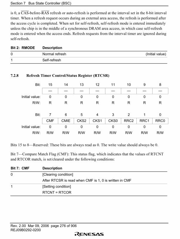
Section 7 Bus State Controller (BSC)
Rev. 2.00 Mar 09, 2006 page 276 of 906REJ09B0292-0200
is 0, a CAS-before-RAS refresh or auto-refresh is performed at the interval set in the 8-bit intervaltimer. When a refresh request occurs during an external area access, the refresh is performed afterthe access cycle is completed. When set for self-refresh, self-refresh mode is entered immediatelyunless the chip is in the middle of a synchronous DRAM area access, in which case self-refreshmode is entered when the access ends. Refresh requests from the interval timer are ignored duringself-refresh.
Bit 2: RMODE Description
0 Normal refresh (Initial value)
1 Self-refresh
7.2.8 Refresh Timer Control/Status Register (RTCSR)
Bit: 15 14 13 12 11 10 9 8
� � � � � � � �
Initial value: 0 0 0 0 0 0 0 0
R/W: R R R R R R R R
Bit: 7 6 5 4 3 2 1 0
CMF CMIE CKS2 CKS1 CKS0 RRC2 RRC1 RRC0
Initial value: 0 0 0 0 0 0 0 0
R/W: R/W R/W R/W R/W R/W R/W R/W R/W
Bits 15 to 8�Reserved: These bits are always read as 0. The write value should always be 0.
Bit 7�Compare Match Flag (CMF): This status flag, which indicates that the values of RTCNTand RTCOR match, is set/cleared under the following conditions:
Bit 7: CMF Description
0 [Clearing condition]
After RTCSR is read when CMF is 1, 0 is written in CMF
1 [Setting condition]
RTCNT = RTCOR
Section 7 Bus State Controller (BSC)
Rev. 2.00 Mar 09, 2006 page 277 of 906REJ09B0292-0200
Bit 6�Compare Match Interrupt Enable (CMIE): Enables or disables an interrupt request causedby the CMF bit of RTCSR when CMF is set to 1.
Bit 6: CMIE Description
0 Interrupt request caused by CMF is disabled (Initial value)
1 Interrupt request caused by CMF is enabled
Bits 5 to 3�Clock Select Bits (CKS2�CKS0)
Bit 5: CKS2 Bit 4: CKS1 Bit 3: CKS0 Description
0 0 0 Count-up disabled (Initial value)
1 Pφ/4
1 0 Pφ/16
1 Pφ/64
1 0 0 Pφ/256
1 Pφ/1024
1 0 Pφ/2048
1 Pφ/4096
Bits 2 to 0�Refresh Count (RRC2�RRC0): These bits specify the number of consecutiverefreshes to be performed when the refresh timer counter (RTCNT) and refresh time constantregister (RTCOR) values match and a refresh request is issued.
Bit 2: RRC2 Bit 1: RRC1 Bit 0: RRC0 Description
0 0 0 1 refresh (Initial value)
1 2 refreshes
1 0 4 refreshes
1 6 refreshes
1 0 0 8 refreshes
1 Reserved (do not set)
1 0 Reserved (do not set)
1 Reserved (do not set)
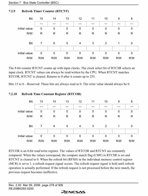
Section 7 Bus State Controller (BSC)
Rev. 2.00 Mar 09, 2006 page 278 of 906REJ09B0292-0200
7.2.9 Refresh Timer Counter (RTCNT)
Bit: 15 14 13 12 11 10 9 8
� � � � � � � �
Initial value: 0 0 0 0 0 0 0 0
R/W: R R R R R R R R
Bit: 7 6 5 4 3 2 1 0
Initial value: 0 0 0 0 0 0 0 0
R/W: R/W R/W R/W R/W R/W R/W R/W R/W
The 8-bit counter RTCNT counts up with input clocks. The clock select bit of RTCSR selects aninput clock. RTCNT values can always be read/written by the CPU. When RTCNT matchesRTCOR, RTCNT is cleared. Returns to 0 after it counts up to 255.
Bits 15 to 8�Reserved: These bits are always read as 0. The write value should always be 0.
7.2.10 Refresh Time Constant Register (RTCOR)
Bit: 15 14 13 12 11 10 9 8
� � � � � � � �
Initial value: 0 0 0 0 0 0 0 0
R/W: R R R R R R R R
Bit: 7 6 5 4 3 2 1 0
Initial value: 0 0 0 0 0 0 0 0
R/W: R/W R/W R/W R/W R/W R/W R/W R/W
RTCOR is an 8-bit read/write register. The values of RTCOR and RTCNT are constantlycompared. When the values correspond, the compare match flag (CMF) in RTCSR is set andRTCNT is cleared to 0. When the refresh bit (RFSH) in the individual memory control register(MCR) is set to 1, a refresh request signal occurs. The refresh request signal is held until refreshoperation is actually performed. If the refresh request is not processed before the next match, theprevious request becomes ineffective.

Section 7 Bus State Controller (BSC)
Rev. 2.00 Mar 09, 2006 page 279 of 906REJ09B0292-0200
When the CMIE bit in RTCSR is set to 1, an interrupt request is sent to the controller by thismatch signal. The interrupt request is output continuously until the CMF bit in RTCSR is cleared.When the CMF bit clears, it only affects the interrupt; the refresh request is not cleared by thisoperation. When a refresh is performed and refresh requests are counted using interrupts, a refreshcan be set simultaneously with the interval timer interrupt.
Bits 15 to 8�Reserved: These bits are always read as 0. The write value should always be 0.
7.3 Access Size and Data Alignment
7.3.1 Connection to Ordinary Devices
Byte, word, and longword are supported as access units. Data is aligned based on the data width ofthe device. Therefore, reading longword data from a byte-width device requires four readoperations. The bus state controller automatically converts data alignment and data length betweeninterfaces. An 8-bit, 16-bit, or 32-bit external device data width can be connected by using themode pins for the CS0 space, or by setting BCR2 for the CS1�CS4 spaces. However, the datawidth of devices connected to the respective spaces is specified statically, and the data widthcannot be changed for each access cycle. Figures 7.5 to 7.7 show the relationship between devicedata widths and access units.
D31
7 0
D23 D15 D7 D0
15 8 7 0
7 07 0
7 0
A24–A0000000000001000002000003000000000002000000
Data input/output pinByte read/write of address 0Byte read/write of address 1Byte read/write of address 2Byte read/write of address 3Word read/write of address 0Word read/write of address 2Longword read/write of address 031 24 23 16
15 8 7 015 8 7 0
32-bit external device (ordinary)
Figure 7.5 32-Bit External Devices and Their Access Units
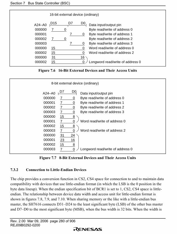
Section 7 Bus State Controller (BSC)
Rev. 2.00 Mar 09, 2006 page 280 of 906REJ09B0292-0200
D15
7 0
D7
16-bit external device (ordinary)
D0
15 0
7 07 0
7 0
A24–A0000000000001000002000003000000000002000000000002
Data input/output pinByte read/write of address 0Byte read/write of address 1Byte read/write of address 2Byte read/write of address 3Word read/write of address 0Word read/write of address 2
Longword read/write of address 0
15 031 1615 0
Figure 7.6 16-Bit External Devices and Their Access Units
D7
8-bit external device (ordinary)
7 0
D0
7 07 07 015 87 015 87 031 2423 1615 87 0
A24–A0000000000001000002000003000000000001000002000003000000000001000002000003
Data input/output pinByte read/write of address 0Byte read/write of address 1Byte read/write of address 2Byte read/write of address 3
Word read/write of address 0
Word read/write of address 2
Longword read/write of address 0
Figure 7.7 8-Bit External Devices and Their Access Units
7.3.2 Connection to Little-Endian Devices
The chip provides a conversion function in CS2, CS4 space for connection to and to maintain datacompatibility with devices that use little-endian format (in which the LSB is the 0 position in thebyte data lineup). When the endian specification bit of BCR1 is set to 1, CS2, CS4 space is little-endian. The relationship between device data width and access unit for little-endian format isshown in figures 7.8, 7.9, and 7.10. When sharing memory or the like with a little-endian busmaster, the SH7616 connects D31�D24 to the least significant byte (LSB) of the other bus masterand D7�D0 to the most significant byte (MSB), when the bus width is 32 bits. When the width is
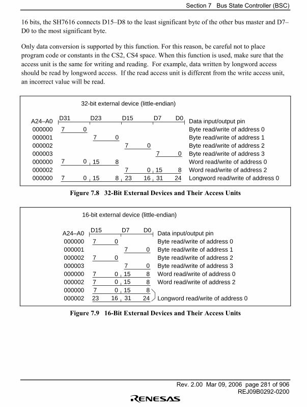
Section 7 Bus State Controller (BSC)
Rev. 2.00 Mar 09, 2006 page 281 of 906REJ09B0292-0200
16 bits, the SH7616 connects D15�D8 to the least significant byte of the other bus master and D7�D0 to the most significant byte.
Only data conversion is supported by this function. For this reason, be careful not to placeprogram code or constants in the CS2, CS4 space. When this function is used, make sure that theaccess unit is the same for writing and reading. For example, data written by longword accessshould be read by longword access. If the read access unit is different from the write access unit,an incorrect value will be read.
D31
7 0
7 0
7 0
D23 D15
32-bit external device (little-endian)
D7 D0
15 8
7 07 0
7 0
A24–A0000000000001000002000003000000000002000000
Data input/output pinByte read/write of address 0Byte read/write of address 1Byte read/write of address 2Byte read/write of address 3Word read/write of address 0Word read/write of address 2Longword read/write of address 015 8
7 0 15 823 16 31 24
Figure 7.8 32-Bit External Devices and Their Access Units
D15
7 0
D7
16-bit external device (little-endian)
D0
7 8
7 07 0
0715
0 150 15
16 31
0
A24–A0000000000001000002000003000000000002000000000002
Data input/output pinByte read/write of address 0Byte read/write of address 1Byte read/write of address 2Byte read/write of address 3Word read/write of address 0Word read/write of address 2
Longword read/write of address 0
7 87 823 24
Figure 7.9 16-Bit External Devices and Their Access Units
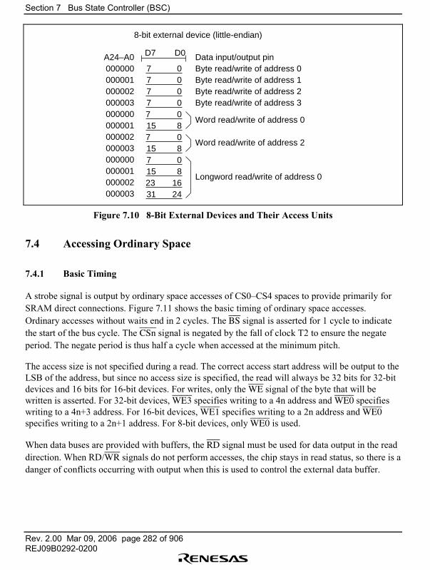
Section 7 Bus State Controller (BSC)
Rev. 2.00 Mar 09, 2006 page 282 of 906REJ09B0292-0200
D7
7 0
D0
7 07 07 07 015 87 015 87 015 823 1631 24
A24–A0000000000001000002000003000000000001000002000003000000000001000002000003
Data input/output pinByte read/write of address 0Byte read/write of address 1Byte read/write of address 2Byte read/write of address 3
Word read/write of address 0
Word read/write of address 2
Longword read/write of address 0
8-bit external device (little-endian)
Figure 7.10 8-Bit External Devices and Their Access Units
7.4 Accessing Ordinary Space
7.4.1 Basic Timing
A strobe signal is output by ordinary space accesses of CS0�CS4 spaces to provide primarily forSRAM direct connections. Figure 7.11 shows the basic timing of ordinary space accesses.Ordinary accesses without waits end in 2 cycles. The BS signal is asserted for 1 cycle to indicatethe start of the bus cycle. The CSn signal is negated by the fall of clock T2 to ensure the negateperiod. The negate period is thus half a cycle when accessed at the minimum pitch.
The access size is not specified during a read. The correct access start address will be output to theLSB of the address, but since no access size is specified, the read will always be 32 bits for 32-bitdevices and 16 bits for 16-bit devices. For writes, only the WE signal of the byte that will bewritten is asserted. For 32-bit devices, WE3 specifies writing to a 4n address and WE0 specifieswriting to a 4n+3 address. For 16-bit devices, WE1 specifies writing to a 2n address and WE0specifies writing to a 2n+1 address. For 8-bit devices, only WE0 is used.
When data buses are provided with buffers, the RD signal must be used for data output in the readdirection. When RD/WR signals do not perform accesses, the chip stays in read status, so there is adanger of conflicts occurring with output when this is used to control the external data buffer.
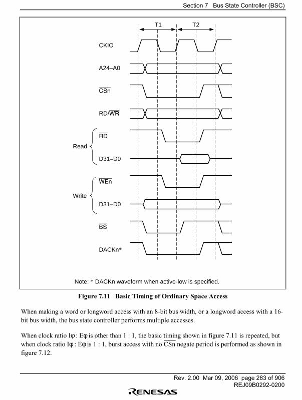
Section 7 Bus State Controller (BSC)
Rev. 2.00 Mar 09, 2006 page 283 of 906REJ09B0292-0200
T1 T2
CKIO
A24–A0
CSn
RD/WR
RD
D31–D0
WEn
D31–D0
BS
DACKn*
Read
Write
Note: * DACKn waveform when active-low is specified.
Figure 7.11 Basic Timing of Ordinary Space Access
When making a word or longword access with an 8-bit bus width, or a longword access with a 16-bit bus width, the bus state controller performs multiple accesses.
When clock ratio Iφ : Eφ is other than 1 : 1, the basic timing shown in figure 7.11 is repeated, butwhen clock ratio Iφ : Eφ is 1 : 1, burst access with no CSn negate period is performed as shown infigure 7.12.
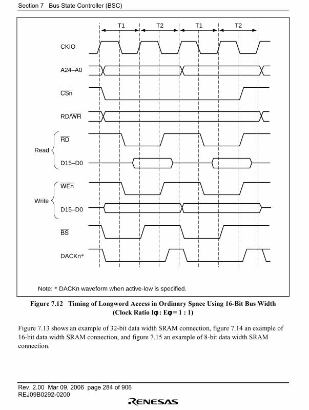
Section 7 Bus State Controller (BSC)
Rev. 2.00 Mar 09, 2006 page 284 of 906REJ09B0292-0200
T1 T2
CKIO
A24–A0
CSn
RD/WR
RD
D15–D0
WEn
D15–D0
BS
DACKn*
Read
Write
T1 T2
Note: * DACKn waveform when active-low is specified.
Figure 7.12 Timing of Longword Access in Ordinary Space Using 16-Bit Bus Width(Clock Ratio Iφφφφ : Eφφφφ = 1 : 1)
Figure 7.13 shows an example of 32-bit data width SRAM connection, figure 7.14 an example of16-bit data width SRAM connection, and figure 7.15 an example of 8-bit data width SRAMconnection.
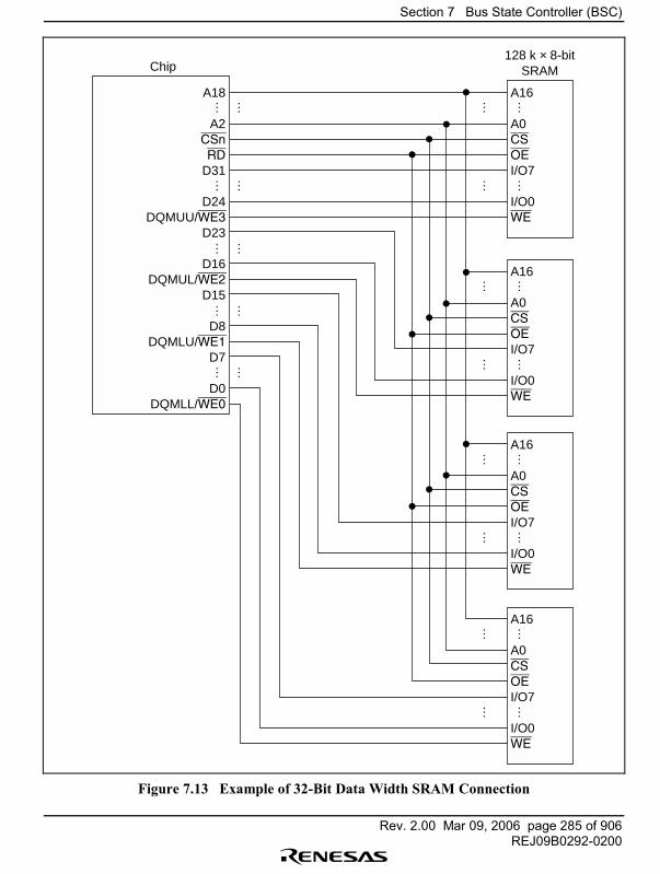
Section 7 Bus State Controller (BSC)
Rev. 2.00 Mar 09, 2006 page 285 of 906REJ09B0292-0200
A18
A2CSn
RD
D31
D24DQMUU/WE3
D23
D16DQMUL/WE2
D15
D8DQMLU/WE1
D7
D0DQMLL/WE0
A16
A0CS
OE
I/O7
I/O0WE
Chip128 k × 8-bit
SRAM
… …
…
……
……
A16
A0CS
OE
I/O7
I/O0WE
……
……
A16
A0CS
OE
I/O7
I/O0WE
……
……
A16
A0CS
OE
I/O7
I/O0WE
……
……
…
… …
… …
… …
Figure 7.13 Example of 32-Bit Data Width SRAM Connection
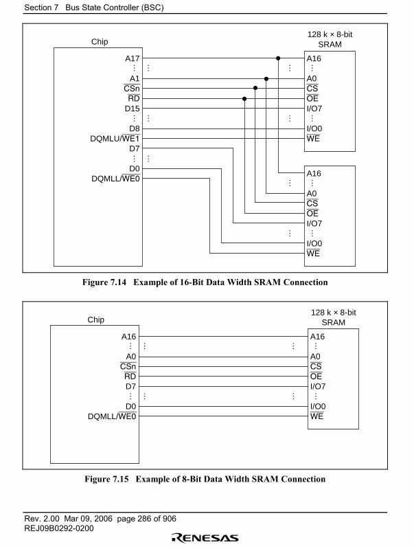
Section 7 Bus State Controller (BSC)
Rev. 2.00 Mar 09, 2006 page 286 of 906REJ09B0292-0200
A17
A1CSn
RD
D15
D8DQMLU/WE1
D7
D0DQMLL/WE0
A16
A0CS
OE
I/O7
I/O0WE
Chip128 k × 8-bit
SRAM
… …
…
……
……
A16
A0CS
OE
I/O7
I/O0WE
……
……
…
… …
Figure 7.14 Example of 16-Bit Data Width SRAM Connection
A16
A0CSn
RD
D7
D0DQMLL/WE0
A16
A0CS
OE
I/O7
I/O0WE
Chip128 k × 8-bit
SRAM
… …
…
……
………
Figure 7.15 Example of 8-Bit Data Width SRAM Connection
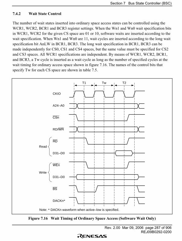
Section 7 Bus State Controller (BSC)
Rev. 2.00 Mar 09, 2006 page 287 of 906REJ09B0292-0200
7.4.2 Wait State Control
The number of wait states inserted into ordinary space access states can be controlled using theWCR1, WCR2, BCR1 and BCR3 register settings. When the Wn1 and Wn0 wait specification bitsin WCR1, WCR2 for the given CS space are 01 or 10, software waits are inserted according to thewait specification. When Wn1 and Wn0 are 11, wait cycles are inserted according to the long waitspecification bit AnLW in BCR1, BCR3. The long wait specification in BCR1, BCR3 can bemade independently for CS0, CS1 and CS4 spaces, but the same value must be specified for CS2and CS3 spaces. All WCR1 specifications are independent. By means of WCR1, WCR2, BCR1,and BCR3, a Tw cycle is inserted as a wait cycle as long as the number of specified cycles at thewait timing for ordinary access space shown in figure 7.16. The names of the control bits thatspecify Tw for each CS space are shown in table 7.5.
T1 Tw
CKIO
A24–A0
CSn
RD/WR
RD
D31–D0
WEn
D31–D0
BS
DACKn*
Read
Write
T2
Note: * DACKn waveform when active–low is specified.
Figure 7.16 Wait Timing of Ordinary Space Access (Software Wait Only)
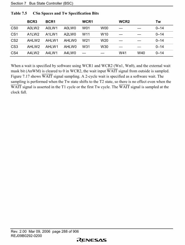
Section 7 Bus State Controller (BSC)
Rev. 2.00 Mar 09, 2006 page 288 of 906REJ09B0292-0200
Table 7.5 CSn Spaces and Tw Specification Bits
BCR3 BCR1 WCR1 WCR2 Tw
CS0 A0LW2 A0LW1 A0LW0 W01 W00 � � 0�14
CS1 A1LW2 A1LW1 A2LW0 W11 W10 � � 0�14
CS2 AHLW2 AHLW1 AHLW0 W21 W20 � � 0�14
CS3 AHLW2 AHLW1 AHLW0 W31 W30 � � 0�14
CS4 A4LW2 A4LW1 A4LW0 � � W41 W40 0�14
When a wait is specified by software using WCR1 and WCR2 (Wn1, Wn0), and the external waitmask bit (AnWM) is cleared to 0 in WCR2, the wait input WAIT signal from outside is sampled.Figure 7.17 shows WAIT signal sampling. A 2-cycle wait is specified as a software wait. Thesampling is performed when the Tw state shifts to the T2 state, so there is no effect even when theWAIT signal is asserted in the T1 cycle or the first Tw cycle. The WAIT signal is sampled at theclock fall.

Section 7 Bus State Controller (BSC)
Rev. 2.00 Mar 09, 2006 page 289 of 906REJ09B0292-0200
T1 Tw
CKIO
A24–A0
CSn
RD/WR
RD
D31–D0
WEn
D31–D0
WAIT
BS
DACKn*
Read
Write
Tw Twx T2
Wait statesfrom WAIT
signal input
Note: * DACKn waveform when active-low is specified.
Figure 7.17 Wait State Timing of Ordinary Space Access(Wait States from WAITWAITWAITWAIT Signal)

Section 7 Bus State Controller (BSC)
Rev. 2.00 Mar 09, 2006 page 290 of 906REJ09B0292-0200
For the CS0�CS3 spaces, CSn, RD, and WEn are negated for one cycle after negation of theexternal wait signal is accepted, as shown in figure 7.17. For the CS4 space, the number of cyclesbefore CSn, RD, and WEn are negated after acceptance of external wait negation can be set as 1,2, or 4 by means of bits A4WD1 and A4WD0 in WCR2. Figure 7.18 shows an example.
T1 Tw
CKIO
A24–A0
CSn
RD/WR
RD
D15–D0
WEn
D15–D0
WAIT
BS
DACKn*
Read
Write
Twx Twx T2
Specified by A4WD1 and A4WD0 in WCR2 (A4WD1, A4WD0 = 01)
Note: * DACKn waveform when active-low is specified.
Figure 7.18 Wait State Timing of Ordinary Space in CS4 Space
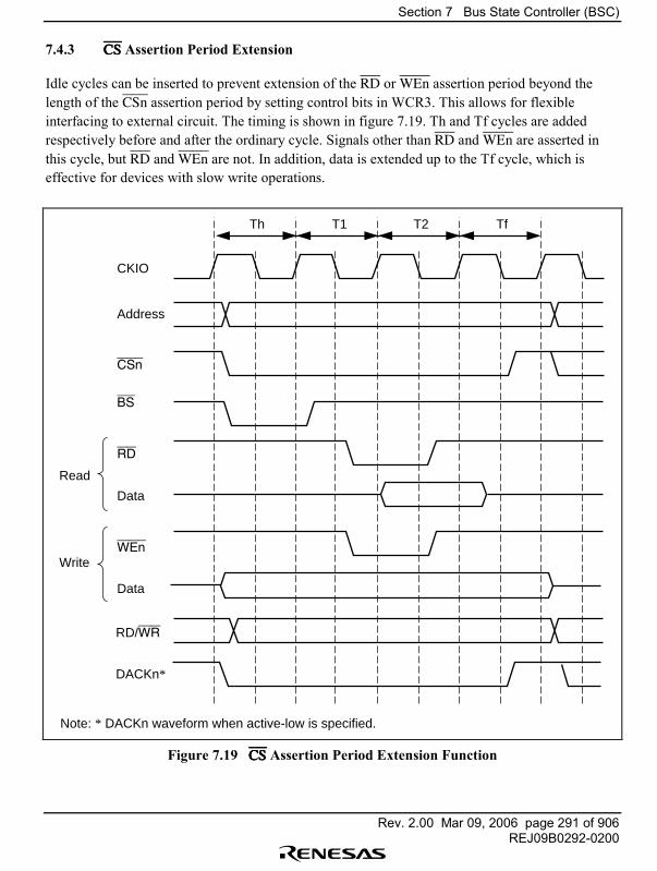
Section 7 Bus State Controller (BSC)
Rev. 2.00 Mar 09, 2006 page 291 of 906REJ09B0292-0200
7.4.3 CSCSCSCS Assertion Period Extension
Idle cycles can be inserted to prevent extension of the RD or WEn assertion period beyond thelength of the CSn assertion period by setting control bits in WCR3. This allows for flexibleinterfacing to external circuit. The timing is shown in figure 7.19. Th and Tf cycles are addedrespectively before and after the ordinary cycle. Signals other than RD and WEn are asserted inthis cycle, but RD and WEn are not. In addition, data is extended up to the Tf cycle, which iseffective for devices with slow write operations.
CKIO
Address
CSn
BS
RD
Data
WEn
Data
Th T1 T2 Tf
DACKn*
RD/WR
Read
Write
Note: * DACKn waveform when active-low is specified.
Figure 7.19 CSCSCSCS Assertion Period Extension Function
Section 7 Bus State Controller (BSC)
Rev. 2.00 Mar 09, 2006 page 292 of 906REJ09B0292-0200
For the CS0�CS4 spaces, For spaces CS0�CS4, Th and Tf can be set as follows.
Th Tf WCR3
CS0�3 0�2 0�2 AnSW1, AnSW0 (Th = Tf) n =0�3
CS4 0�7 0�5 Th: A4SW2�0Tf: A4HW1�0
7.5 Synchronous DRAM Interface
7.5.1 Synchronous DRAM Direct Connection
Seven kinds of synchronous DRAM can be connected: 2-Mbit (128 k × 16), 4-Mbit (256 k × 16),16-Mbit (1 M × 16, 2 M × 8, and 4 M × 4), and 64-Mbit (4 M × 16 and 8 M × 8). This chipsupports 64-Mbit synchronous DRAMs internally divided into two or four banks, and othersynchronous DRAMs internally divided into two banks. Since synchronous DRAM can beselected by the CS signal, CS2 and CS3 spaces can be connected using a common RAS or othercontrol signal. When the memory enable bits for DRAM and other memory (DRAM2�DRAM0)in BCR1 are set to 001, CS2 is ordinary space and CS3 is synchronous DRAM space. When theDRAM2�0 bits are set to 100, CS2 is synchronous DRAM space and CS3 is ordinary space. Whenthe bits are set to 101, both CS2 and CS3 are synchronous DRAM spaces.
Supported synchronous DRAM operating modes are burst read/single write mode (initial setting)and burst read/burst write mode. The burst length depends on the data bus width, comprising 8bursts for a 16-bit width, and 4 bursts for a 32-bit width. The data bus width is specified by the SZbit in MCR. Burst operation is always performed, so the burst enable (BE) bit in MCR is ignored.Switching to burst write mode is performed by means of the BWE bit in BCR3.
Control signals for directly connecting synchronous DRAM are the RAS, CAS/OE, RD/WR, CS2or CS3, DQMUU, DQMUL, DQMLU, DQMLL, and CKE signals. Signals other than CS2 andCS3 are common to every area, and signals other than CKE are valid and fetched only when CS2or CS3 is true. Therefore, synchronous DRAM can be connected in parallel in multiple areas. CKEis negated (to the low level) only when a self-refresh is performed; otherwise it is always asserted(to the high level).
Commands can be specified for synchronous DRAM using the RAS, CAS/OE, RD/WR, andcertain address signals. These commands are NOP, auto-refresh (REF), self-refresh (SELF), all-bank precharge (PALL), specific bank precharge (PRE), row address strobe/bank active (ACTV),read (READ), read with precharge (READA), write (WRIT), write with precharge (WRITA), andmode register write (MRS).
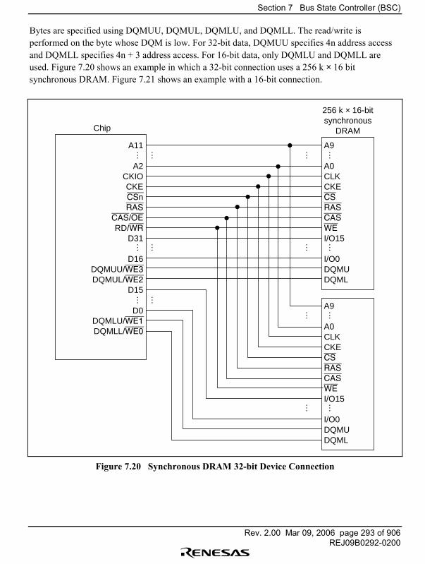
Section 7 Bus State Controller (BSC)
Rev. 2.00 Mar 09, 2006 page 293 of 906REJ09B0292-0200
Bytes are specified using DQMUU, DQMUL, DQMLU, and DQMLL. The read/write isperformed on the byte whose DQM is low. For 32-bit data, DQMUU specifies 4n address accessand DQMLL specifies 4n + 3 address access. For 16-bit data, only DQMLU and DQMLL areused. Figure 7.20 shows an example in which a 32-bit connection uses a 256 k × 16 bitsynchronous DRAM. Figure 7.21 shows an example with a 16-bit connection.
A11
A2CKIOCKECSn
RAS
CAS/OE
RD/WR
D31
D16DQMUU/WE3
DQMUL/WE2
D15
D0DQMLU/WE1
DQMLL/WE0
A9
A0CLKCKECS
RAS
CAS
WE
I/O15
I/O0DQMUDQML
Chip
256 k × 16-bitsynchronous
DRAM… …
… …
… …
……
A9
A0CLKCKECS
RAS
CAS
WE
I/O15
I/O0DQMUDQML
……
……
……
Figure 7.20 Synchronous DRAM 32-bit Device Connection
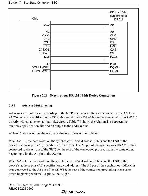
Section 7 Bus State Controller (BSC)
Rev. 2.00 Mar 09, 2006 page 294 of 906REJ09B0292-0200
A10
A1CKIOCKECSn
RAS
CAS/OE
RD/WR
D15
D0DQMLU/WE1
DQMLL/WE0
A9
A0CLKCKECS
RAS
CAS
WE
I/O15
I/O0DQMUDQML
Chip
256 k × 16-bitsynchronous
DRAM
… …
… …
……
……
Figure 7.21 Synchronous DRAM 16-bit Device Connection
7.5.2 Address Multiplexing
Addresses are multiplexed according to the MCR�s address multiplex specification bits AMX2�AMX0 and size specification bit SZ so that synchronous DRAMs can be connected to the SH7616directly without an external multiplex circuit. Table 7.6 shows the relationship between themultiplex specification bits and bit output to the address pins.
A24�A16 always output the original value regardless of multiplexing.
When SZ = 0, the data width on the synchronous DRAM side is 16 bits and the LSB of thedevice�s address pins (A0) specifies word address. The A0 pin of the synchronous DRAM is thusconnected to the A1 pin of the SH7616, the rest of the connection proceeding in the same order,beginning with the A1 pin to the A2 pin.
When SZ = 1, the data width on the synchronous DRAM side is 32 bits and the LSB of thedevice�s address pins (A0) specifies longword address. The A0 pin of the synchronous DRAM isthus connected to the A2 pin of the SH7616, the rest of the connection proceeding in the sameorder, beginning with the A1 pin to the A3 pin.
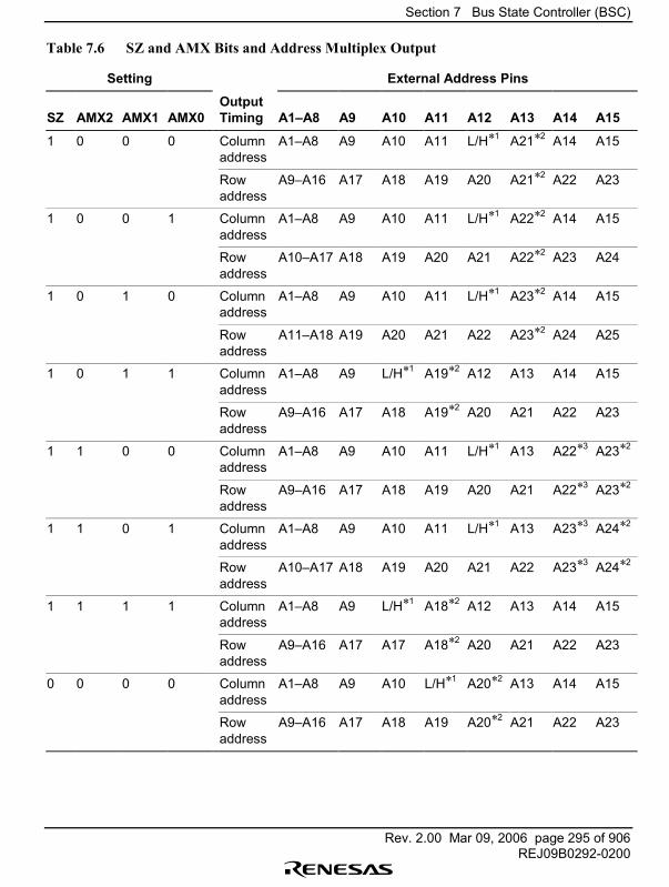
Section 7 Bus State Controller (BSC)
Rev. 2.00 Mar 09, 2006 page 295 of 906REJ09B0292-0200
Table 7.6 SZ and AMX Bits and Address Multiplex Output
Setting External Address Pins
SZ AMX2 AMX1 AMX0OutputTiming A1�A8 A9 A10 A11 A12 A13 A14 A15
1 0 0 0 Columnaddress
A1�A8 A9 A10 A11 L/H*1 A21*2 A14 A15
Rowaddress
A9�A16 A17 A18 A19 A20 A21*2 A22 A23
1 0 0 1 Columnaddress
A1�A8 A9 A10 A11 L/H*1 A22*2 A14 A15
Rowaddress
A10�A17 A18 A19 A20 A21 A22*2 A23 A24
1 0 1 0 Columnaddress
A1�A8 A9 A10 A11 L/H*1 A23*2 A14 A15
Rowaddress
A11�A18 A19 A20 A21 A22 A23*2 A24 A25
1 0 1 1 Columnaddress
A1�A8 A9 L/H*1 A19*2 A12 A13 A14 A15
Rowaddress
A9�A16 A17 A18 A19*2 A20 A21 A22 A23
1 1 0 0 Columnaddress
A1�A8 A9 A10 A11 L/H*1 A13 A22*3 A23*2
Rowaddress
A9�A16 A17 A18 A19 A20 A21 A22*3 A23*2
1 1 0 1 Columnaddress
A1�A8 A9 A10 A11 L/H*1 A13 A23*3 A24*2
Rowaddress
A10�A17 A18 A19 A20 A21 A22 A23*3 A24*2
1 1 1 1 Columnaddress
A1�A8 A9 L/H*1 A18*2 A12 A13 A14 A15
Rowaddress
A9�A16 A17 A17 A18*2 A20 A21 A22 A23
0 0 0 0 Columnaddress
A1�A8 A9 A10 L/H*1 A20*2 A13 A14 A15
Rowaddress
A9�A16 A17 A18 A19 A20*2 A21 A22 A23
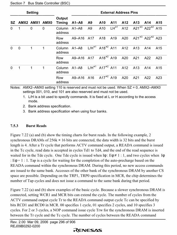
Section 7 Bus State Controller (BSC)
Rev. 2.00 Mar 09, 2006 page 296 of 906REJ09B0292-0200
Setting External Address Pins
SZ AMX2 AMX1 AMX0OutputTiming A1�A8 A9 A10 A11 A12 A13 A14 A15
0 1 0 0 Columnaddress
A1�A8 A9 A10 LH*1 A12 A21*3 A22*2 A15
Rowaddress
A9�A16 A17 A18 A19 A20 A21*3 A22*2 A23
0 0 1 1 Columnaddress
A1�A8 L/H*1 A18*2 A11 A12 A13 A14 A15
Rowaddress
A9�A16 A17 A18*2 A19 A20 A21 A22 A23
0 1 1 1 Columnaddress
A1�A8 L/H*1 A17*2 A11 A12 A13 A14 A15
Rowaddress
A9�A16 A16 A17*2 A19 A20 A21 A22 A23
Notes: AMX2�AMX0 setting 110 is reserved and must not be used. When SZ = 0, AMX2�AMX0settings 001, 010, and 101 are also reserved and must not be used.1. L/H is a bit used to specify commands. It is fixed at L or H according to the access
mode.2. Bank address specification.3. Bank address specification when using four banks.
7.5.3 Burst Reads
Figure 7.22 (a) and (b) show the timing charts for burst reads. In the following example, 2synchronous DRAMs of 256k × 16 bits are connected, the data width is 32 bits and the burstlength is 4. After a Tr cycle that performs ACTV command output, a READA command is issuedin the Tc cycle, read data is accepted in cycles Td1 to Td4, and the end of the read sequence iswaited for in the Tde cycle. One Tde cycle is issued when Iφ : Eφ ≠ 1 : 1, and two cycles when Iφ: Eφ = 1 : 1. Tap is a cycle for waiting for the completion of the auto-precharge based on theREADA command within the synchronous DRAM. During this period, no new access commandsare issued to the same bank. Accesses of the other bank of the synchronous DRAM by another CSspace are possible. Depending on the TRP1, TRP0 specification in MCR, the chip determines thenumber of Tap cycles and does not issue a command to the same bank during that period.
Figure 7.22 (a) and (b) show examples of the basic cycle. Because a slower synchronous DRAM isconnected, setting WCR1 and MCR bits can extend the cycle. The number of cycles from theACTV command output cycle Tr to the READA command output cycle Tc can be specified bybits RCD1 and RCD0 in MCR. 00 specifies 1 cycle, 01 specifies 2 cycles, and 10 specifies 3cycles. For 2 or 3 cycles, a NOP command issue cycle Trw for the synchronous DRAM is insertedbetween the Tr cycle and the Tc cycle. The number of cycles between the READA command
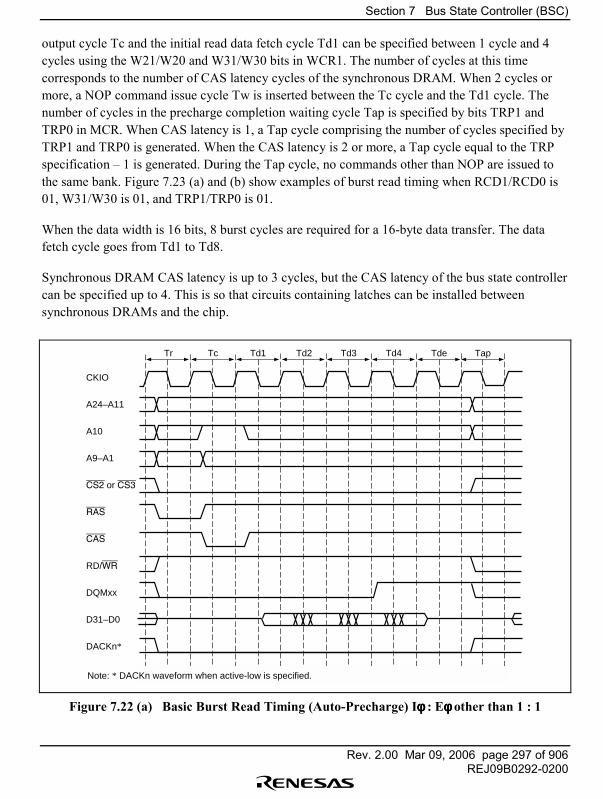
Section 7 Bus State Controller (BSC)
Rev. 2.00 Mar 09, 2006 page 297 of 906REJ09B0292-0200
output cycle Tc and the initial read data fetch cycle Td1 can be specified between 1 cycle and 4cycles using the W21/W20 and W31/W30 bits in WCR1. The number of cycles at this timecorresponds to the number of CAS latency cycles of the synchronous DRAM. When 2 cycles ormore, a NOP command issue cycle Tw is inserted between the Tc cycle and the Td1 cycle. Thenumber of cycles in the precharge completion waiting cycle Tap is specified by bits TRP1 andTRP0 in MCR. When CAS latency is 1, a Tap cycle comprising the number of cycles specified byTRP1 and TRP0 is generated. When the CAS latency is 2 or more, a Tap cycle equal to the TRPspecification � 1 is generated. During the Tap cycle, no commands other than NOP are issued tothe same bank. Figure 7.23 (a) and (b) show examples of burst read timing when RCD1/RCD0 is01, W31/W30 is 01, and TRP1/TRP0 is 01.
When the data width is 16 bits, 8 burst cycles are required for a 16-byte data transfer. The datafetch cycle goes from Td1 to Td8.
Synchronous DRAM CAS latency is up to 3 cycles, but the CAS latency of the bus state controllercan be specified up to 4. This is so that circuits containing latches can be installed betweensynchronous DRAMs and the chip.
Tr Tc
CKIO
A24 –A11
A10
A9–A1
CS2 or CS3
RAS
CAS
RD/WR
DQMxx
D31–D0
DACKn*
Td1 Td2 Td3 Td4 Tde Tap
Note: * DACKn waveform when active-low is specified.
Figure 7.22 (a) Basic Burst Read Timing (Auto-Precharge) Iφφφφ : Eφφφφ other than 1 : 1
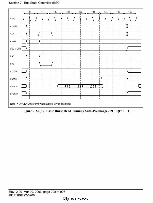
Section 7 Bus State Controller (BSC)
Rev. 2.00 Mar 09, 2006 page 298 of 906REJ09B0292-0200
Tr Tc
CKIO
A24–A11
A10
A9–A1
CS2 or CS3
RAS
CAS
RD/WR
DQMxx
D31–D0
DACKn*
Td1 Td2 Td3 Td4 Tde Tde Tap
Note: * DACKn waveform when active-low is specified.
Figure 7.22 (b) Basic Burst Read Timing (Auto-Precharge) Iφφφφ : Eφφφφ = 1 : 1
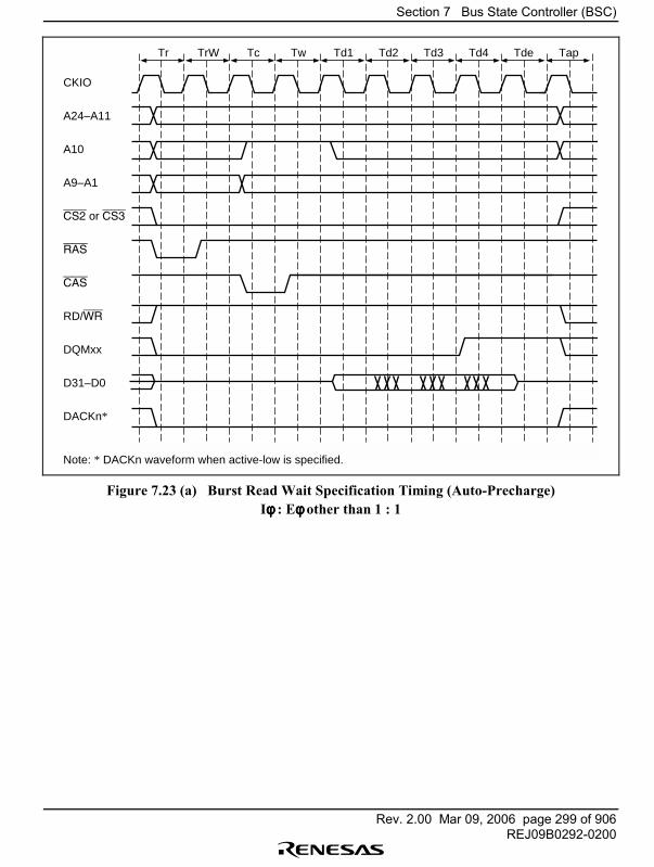
Section 7 Bus State Controller (BSC)
Rev. 2.00 Mar 09, 2006 page 299 of 906REJ09B0292-0200
Tr
CKIO
A24–A11
A10
A9–A1
CS2 or CS3
RAS
CAS
RD/WR
DQMxx
D31–D0
DACKn*
TrW Tc Tw Td1 Td2 Td3 Td4 Tde Tap
Note: * DACKn waveform when active-low is specified.
Figure 7.23 (a) Burst Read Wait Specification Timing (Auto-Precharge)Iφφφφ : Eφφφφ other than 1 : 1
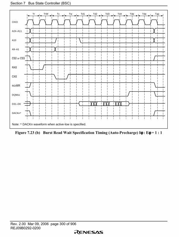
Section 7 Bus State Controller (BSC)
Rev. 2.00 Mar 09, 2006 page 300 of 906REJ09B0292-0200
Tr
CKIO
A24–A11
A10
A9–A1
CS2 or CS3
RAS
CAS
RD/WR
DQMxx
D31–D0
DACKn*
TrW Tc Tw Td1 Td2 Td3 Td4 Tde Tde Tap
Note: * DACKn waveform when active-low is specified.
Figure 7.23 (b) Burst Read Wait Specification Timing (Auto-Precharge) Iφφφφ : Eφφφφ = 1 : 1

Section 7 Bus State Controller (BSC)
Rev. 2.00 Mar 09, 2006 page 301 of 906REJ09B0292-0200
7.5.4 Single Reads
When a cache area is accessed and there is a cache miss, the cache fill cycle is performed in 16-byte units. This means that all the data read in the burst read is valid. On the other hand, when acache-through area is accessed the required data is a maximum length of 32 bits, and theremaining 12 bytes are wasted. The same kind of wasted data access is produced whensynchronous DRAM is specified as the source in a DMA transfer by the DMAC and the transferunit is other than 16 bytes. Figure 7.24 (a) and (b) show the timings of a single address read.Because the synchronous DRAM is set to the burst read mode, the read data output continues afterthe required data is received. To avoid data conflict, an empty read cycle is performed from Td2 toTd4 after the required data is read in Td1 and the device waits for the end of synchronous DRAMoperation.
When the data width is 16 bits, the number of burst transfers during a read is 8. Data is fetched incache-through and other DMA read cycles only in the Td1 and Td2 cycles (of the 8 cycles fromTd1 to Td8) for longword accesses, and only in the Td1 cycle for word or byte accesses.
Empty cycles tend to increase the memory access time, lower the program execution speed, andlower the DMA transfer speed, so it is important to avoid accessing unnecessary cache-throughareas and to use data structures that enable 16-byte unit transfers by placing data on 16-byteboundaries when performing DMA transfers that specify synchronous DRAM as the source.
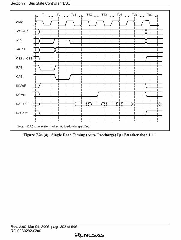
Section 7 Bus State Controller (BSC)
Rev. 2.00 Mar 09, 2006 page 302 of 906REJ09B0292-0200
Tr Tc
CKIO
A24–A11
A10
A9–A1
CS2 or CS3
RAS
CAS
RD/WR
DQMxx
D31–D0
DACKn*
Td1 Td2 Td3 Td4 Tde Tap
Note: * DACKn waveform when active-low is specified.
Figure 7.24 (a) Single Read Timing (Auto-Precharge) Iφφφφ : Eφφφφ other than 1 : 1
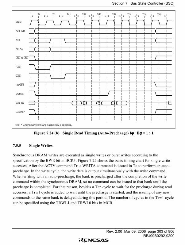
Section 7 Bus State Controller (BSC)
Rev. 2.00 Mar 09, 2006 page 303 of 906REJ09B0292-0200
Tr Tc
CKIO
A24–A11
A10
A9–A1
CS2 or CS3
RAS
CAS
RD/WR
DQMxx
D31–D0
DACKn*
Td1 Td2 Td3 Td4 Tde Tde Tap
Note: * DACKn waveform when active-low is specified.
Figure 7.24 (b) Single Read Timing (Auto-Precharge) Iφφφφ : Eφφφφ = 1 : 1
7.5.5 Single Writes
Synchronous DRAM writes are executed as single writes or burst writes according to thespecification by the BWE bit in BCR3. Figure 7.25 shows the basic timing chart for single writeaccesses. After the ACTV command Tr, a WRITA command is issued in Tc to perform an auto-precharge. In the write cycle, the write data is output simultaneously with the write command.When writing with an auto-precharge, the bank is precharged after the completion of the writecommand within the synchronous DRAM, so no command can be issued to that bank until theprecharge is completed. For that reason, besides a Tap cycle to wait for the precharge during readaccesses, a Trw1 cycle is added to wait until the precharge is started, and the issuing of any newcommands to the same bank is delayed during this period. The number of cycles in the Trw1 cyclecan be specified using the TRWL1 and TRWL0 bits in MCR.

Section 7 Bus State Controller (BSC)
Rev. 2.00 Mar 09, 2006 page 304 of 906REJ09B0292-0200
Tr Tc
CKIO
A24–A11
A10
A9–A1
CS2 or CS3
RAS
CAS
RD/WR
DQMxx
D31–D0
DACKn*
Trwl Tap
Note: * DACKn waveform when active-low is specified.
Figure 7.25 Basic Single Write Cycle Timing (Auto-Precharge)
7.5.6 Burst Write Mode
Burst write mode can be selected by setting the BWE bit to 1 in BCR3. The basic timing charts forburst write access is shown in figure 7.26 (a) and (b). This example assumes a 32-bit bus widthand a burst length of 4. In the burst write cycle, the WRITA command that performs auto-precharge is issued in Tc1 following the ACTV command Tr cycle. The first 4 bytes of write dataare output simultaneously with the WRITA command in Tc1, and the remaining 12 bytes of dataare output consecutively in Tc2, Tc3, and Tc4. In a write with auto-precharge, as with a singlewrite, a Trw1 cycle that provides the waiting time until precharge is started is inserted after outputof the write data, followed by a Tap cycle for the precharge wait in a write access. The Trw1 and
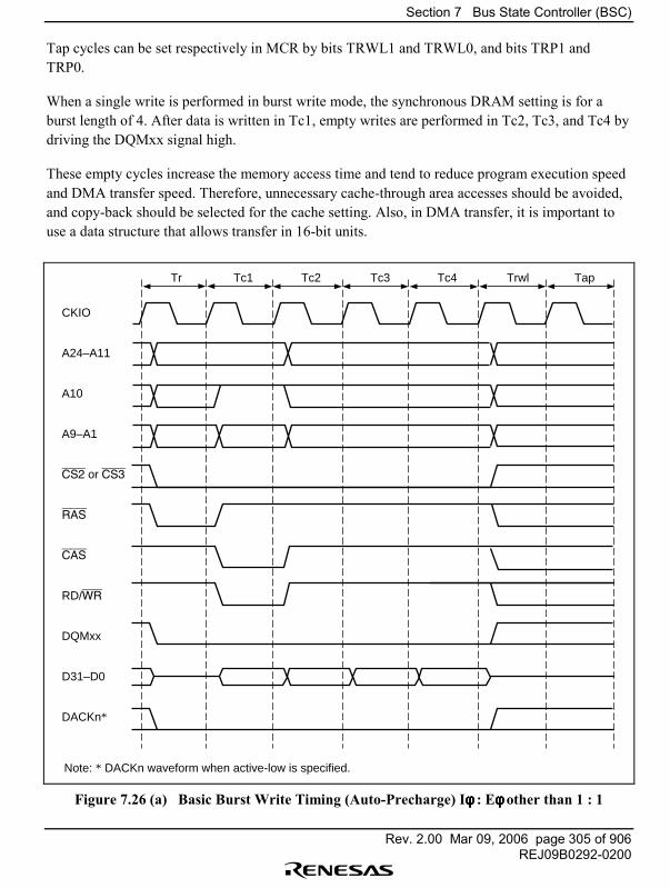
Section 7 Bus State Controller (BSC)
Rev. 2.00 Mar 09, 2006 page 305 of 906REJ09B0292-0200
Tap cycles can be set respectively in MCR by bits TRWL1 and TRWL0, and bits TRP1 andTRP0.
When a single write is performed in burst write mode, the synchronous DRAM setting is for aburst length of 4. After data is written in Tc1, empty writes are performed in Tc2, Tc3, and Tc4 bydriving the DQMxx signal high.
These empty cycles increase the memory access time and tend to reduce program execution speedand DMA transfer speed. Therefore, unnecessary cache-through area accesses should be avoided,and copy-back should be selected for the cache setting. Also, in DMA transfer, it is important touse a data structure that allows transfer in 16-bit units.
Tr Tc1
CKIO
A24–A11
A10
A9–A1
CS2 or CS3
RAS
CAS
RD/WR
DQMxx
D31–D0
DACKn*
Tc2 Tc3 Tc4 Trwl Tap
Note: * DACKn waveform when active-low is specified.
Figure 7.26 (a) Basic Burst Write Timing (Auto-Precharge) Iφφφφ : Eφφφφ other than 1 : 1

Section 7 Bus State Controller (BSC)
Rev. 2.00 Mar 09, 2006 page 306 of 906REJ09B0292-0200
Tr Tc1
CKIO
A24–A11
A10
A9–A1
CS2 or CS3
RAS
CAS
RD/WR
DQMxx
D31–D0
DACKn*
Tc2 Tc3 Tc4 Trwl TapTde
Note: * DACKn waveform when active-low is specified.
Figure 7.26 (b) Basic Burst Write Timing (Auto-Precharge) Iφφφφ : Eφφφφ = 1 : 1
7.5.7 Bank Active Function
A synchronous DRAM bank function is used to support high-speed accesses of the same rowaddress. When the RASD bit in MCR is set to 1, read/write accesses are performed usingcommands without auto-precharge (READ, WRIT). In this case, even when the access iscompleted, no precharge is performed. This function is not supported in the CS2 space. When thebank active function is used, no precharge is performed when the access is completed. Whenaccessing the same row address in the same bank, a READ or WRIT command can be calledimmediately without calling an ACTV command, just like the RAS down mode of the DRAM�shigh-speed page mode. Synchronous DRAM is divided into two banks, so one row address in eachcan stay active. When the next access is to a different row address, a PRE command is called firstto precharge the bank, and access is performed by an ACTV command and READ or WRITcommand in order, after the precharge is completed. With successive accesses to different row
Section 7 Bus State Controller (BSC)
Rev. 2.00 Mar 09, 2006 page 307 of 906REJ09B0292-0200
addresses, the precharge is performed after the access request occurs, so the access time is longer.When writing, performing an auto-precharge means that no command can be called for tRWL +tAP cycles after a WRITA command is called. When the bank active mode is used, READ orWRIT commands can be issued consecutively if the row address is the same. This shortens thenumber of cycles by tRWL + tAP for each write. The number of cycles between the issue of theprecharge command and the row address strobe command is determined by the TRP1, TRP0 inMCR.
Whether execution is faster when the bank active mode is used or when basic access is used isdetermined by the proportion of accesses to the same row address (P1) and the average number ofcycles from the end of one access to the next access (tA). When tA is longer than tAP, the delaywaiting for the precharge during a read becomes invisible. If tA is longer than tRWL + tAP, thedelay waiting for the precharge also becomes invisible during writes. The difference between thebank active mode and basic access speeds in these cases is the number of cycles between the startof access and the issue of the read/write command: (tRP + tRCD) × (1 � P1) and tRCD,respectively.
The time that a bank can be kept active, tRAS, is limited. When the period will be provided byprogram execution, and it is not assured that another row address will be accessed without a hit tothe cache, the synchronous DRAM must be set to auto-refresh and the refresh cycle must be set tothe maximum value tRAS or less. This enables the limit on the maximum active period for eachbank to be ensured. When auto-refresh is not being used, some measure must be taken in theprogram to ensure that the bank does not stay active for longer than the prescribed period.
Figure 7.27 (a) and (b) show burst read cycles that is not an auto-precharge cycle, figure 7.28 (a)and (b) show burst read cycles to a same row address, figure 7.29 (a) and (b) show burst readcycles to different row addresses, figure 7.30 shows a write cycle without auto-precharge, figure7.31 shows a write cycle to a same row address, and figure 7.32 shows a write cycle to differentrow addresses.
In figure 7.28, a cycle that does nothing, Tnop, is inserted before the Tc cycle that issues theREAD command. Synchronous DRAMs have a 2 cycle latency during reads for the DQMxxsignals that specify bytes. If the Tc cycle is performed immediately without inserting a Tnopcycle, the DQMxx signal for the Td1 cycle data output cannot be specified. This is why the Tnopcycle is inserted. When the CAS latency is 2 or more, however, the Tnop cycle is not inserted sothat timing requirements will be met even when a DQMxx signal is set after the Tc cycle.
When the bank active mode is set, the access will start with figure 7.27 or figure 7.30 and repeatfigure 7.28 or figure 7.31 for as long as the same row address continues to be accessed when onlyaccesses to the respective banks of the CS3 space are considered. Accesses to other CS spacesduring this period do not affect this operation. When an access occurs to a different row addresswhile the bank is active, figure 7.29 or figure 7.32 will be substituted for figures 7.28 and 7.31
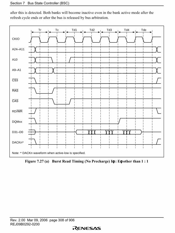
Section 7 Bus State Controller (BSC)
Rev. 2.00 Mar 09, 2006 page 308 of 906REJ09B0292-0200
after this is detected. Both banks will become inactive even in the bank active mode after therefresh cycle ends or after the bus is released by bus arbitration.
Tr Tc
CKIO
A24–A11
A10
A9–A1
CS3
RAS
CAS
RD/WR
DQMxx
D31–D0
DACKn*
Td1 Td2 Td3 Td4 Tde
Note: * DACKn waveform when active-low is specified.
Figure 7.27 (a) Burst Read Timing (No Precharge) Iφφφφ : Eφφφφ other than 1 : 1
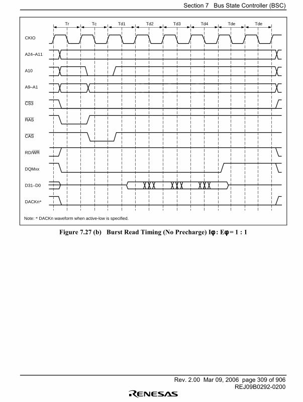
Section 7 Bus State Controller (BSC)
Rev. 2.00 Mar 09, 2006 page 309 of 906REJ09B0292-0200
Tr Tc
CKIO
A24–A11
A10
A9–A1
CS3
RAS
CAS
RD/WR
DQMxx
D31–D0
DACKn*
Td1 Td2 Td3 Td4 Tde Tde
Note: * DACKn waveform when active-low is specified.
Figure 7.27 (b) Burst Read Timing (No Precharge) Iφφφφ : Eφφφφ = 1 : 1
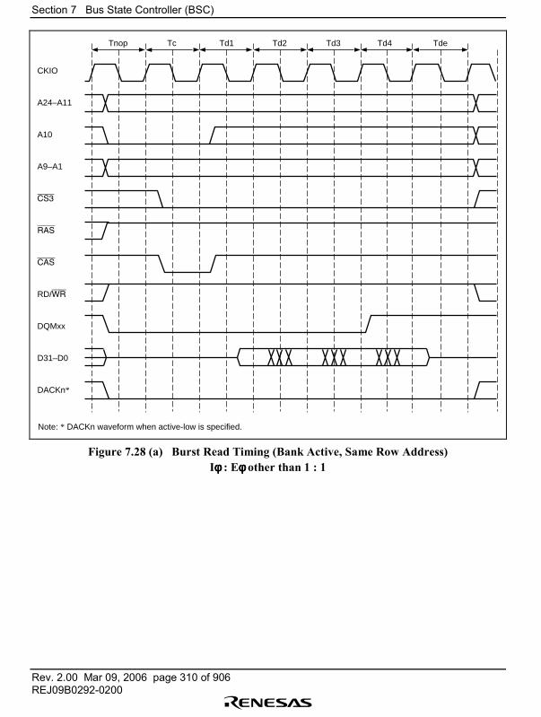
Section 7 Bus State Controller (BSC)
Rev. 2.00 Mar 09, 2006 page 310 of 906REJ09B0292-0200
Tnop
CKIO
A24–A11
A10
A9–A1
CS3
RAS
CAS
RD/WR
DQMxx
D31–D0
DACKn*
Tc Td1 Td2 Td3 Td4 Tde
Note: * DACKn waveform when active-low is specified.
Figure 7.28 (a) Burst Read Timing (Bank Active, Same Row Address)Iφφφφ : Eφφφφ other than 1 : 1
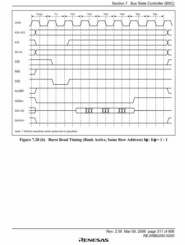
Section 7 Bus State Controller (BSC)
Rev. 2.00 Mar 09, 2006 page 311 of 906REJ09B0292-0200
TcTnop
CKIO
A24–A11
A10
A9–A1
CS3
RAS
CAS
RD/WR
DQMxx
D31–D0
DACKn*
Td1 Td2 Td3 Td4 Tde Tde
Note: * DACKn waveform when active-low is specified.
Figure 7.28 (b) Burst Read Timing (Bank Active, Same Row Address) Iφφφφ : Eφφφφ = 1 : 1
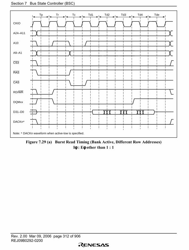
Section 7 Bus State Controller (BSC)
Rev. 2.00 Mar 09, 2006 page 312 of 906REJ09B0292-0200
Tp Tr
CKIO
A24–A11
A10
A9–A1
CS3
RAS
CAS
RD/WR
DQMxx
D31–D0
DACKn*
Tc Td1 Td2 Td3 Td4 Tde
Note: * DACKn waveform when active-low is specified.
Figure 7.29 (a) Burst Read Timing (Bank Active, Different Row Addresses)Iφφφφ : Eφφφφ other than 1 : 1
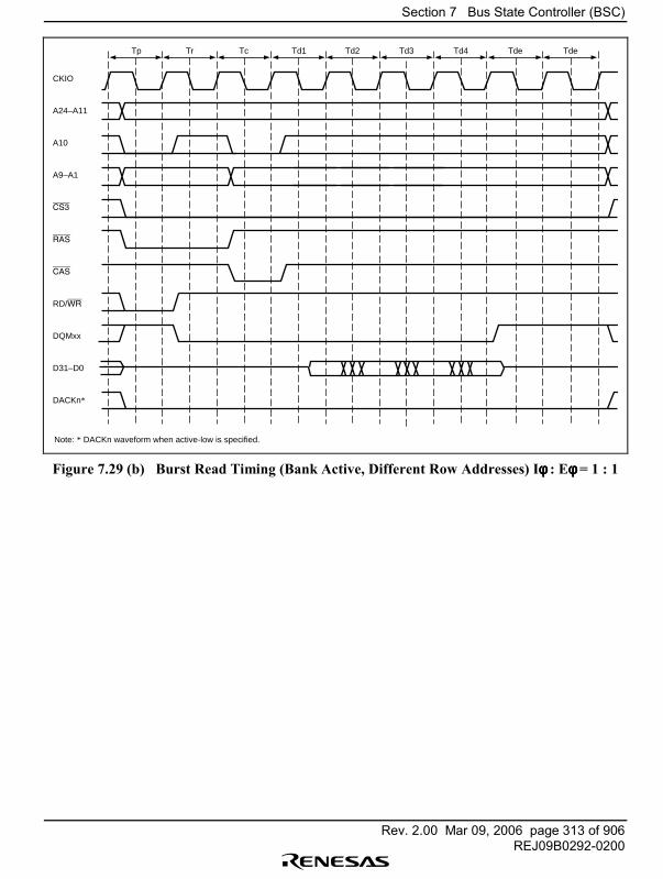
Section 7 Bus State Controller (BSC)
Rev. 2.00 Mar 09, 2006 page 313 of 906REJ09B0292-0200
Tp Tr
CKIO
A24–A11
A10
A9–A1
CS3
RAS
CAS
RD/WR
DQMxx
D31–D0
DACKn*
Tc Td1 Td2 Td3 Td4 Tde Tde
Note: * DACKn waveform when active-low is specified.
Figure 7.29 (b) Burst Read Timing (Bank Active, Different Row Addresses) Iφφφφ : Eφφφφ = 1 : 1
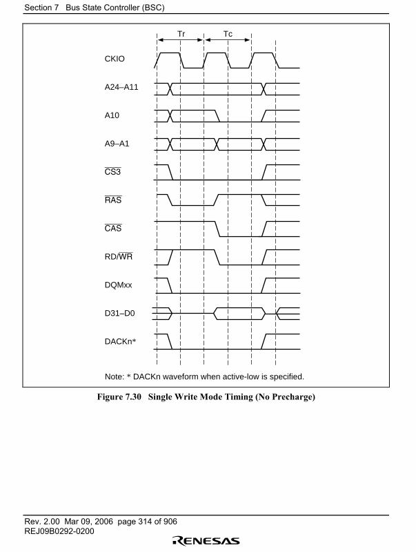
Section 7 Bus State Controller (BSC)
Rev. 2.00 Mar 09, 2006 page 314 of 906REJ09B0292-0200
CKIO
A24–A11
A10
A9–A1
CS3
RAS
CAS
RD/WR
DQMxx
D31–D0
DACKn*
Tr Tc
Note: * DACKn waveform when active-low is specified.
Figure 7.30 Single Write Mode Timing (No Precharge)
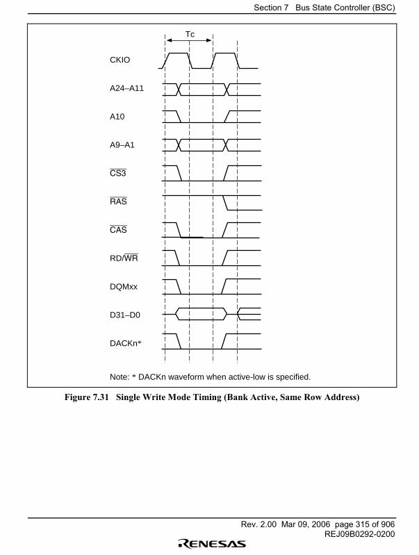
Section 7 Bus State Controller (BSC)
Rev. 2.00 Mar 09, 2006 page 315 of 906REJ09B0292-0200
CKIO
A24–A11
A10
A9–A1
CS3
RAS
CAS
RD/WR
DQMxx
D31–D0
DACKn*
Tc
Note: * DACKn waveform when active-low is specified.
Figure 7.31 Single Write Mode Timing (Bank Active, Same Row Address)
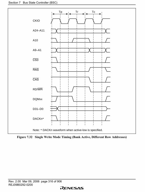
Section 7 Bus State Controller (BSC)
Rev. 2.00 Mar 09, 2006 page 316 of 906REJ09B0292-0200
CKIO
A24–A11
A10
A9–A1
CS3
RAS
CAS
RD/WR
DQMxx
D31–D0
DACKn*
Tp Tr Tc
Note: * DACKn waveform when active-low is specified.
Figure 7.32 Single Write Mode Timing (Bank Active, Different Row Addresses)
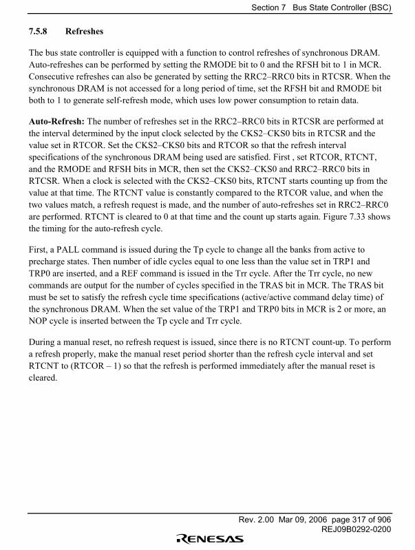
Section 7 Bus State Controller (BSC)
Rev. 2.00 Mar 09, 2006 page 317 of 906REJ09B0292-0200
7.5.8 Refreshes
The bus state controller is equipped with a function to control refreshes of synchronous DRAM.Auto-refreshes can be performed by setting the RMODE bit to 0 and the RFSH bit to 1 in MCR.Consecutive refreshes can also be generated by setting the RRC2�RRC0 bits in RTCSR. When thesynchronous DRAM is not accessed for a long period of time, set the RFSH bit and RMODE bitboth to 1 to generate self-refresh mode, which uses low power consumption to retain data.
Auto-Refresh: The number of refreshes set in the RRC2�RRC0 bits in RTCSR are performed atthe interval determined by the input clock selected by the CKS2�CKS0 bits in RTCSR and thevalue set in RTCOR. Set the CKS2�CKS0 bits and RTCOR so that the refresh intervalspecifications of the synchronous DRAM being used are satisfied. First , set RTCOR, RTCNT,and the RMODE and RFSH bits in MCR, then set the CKS2�CKS0 and RRC2�RRC0 bits inRTCSR. When a clock is selected with the CKS2�CKS0 bits, RTCNT starts counting up from thevalue at that time. The RTCNT value is constantly compared to the RTCOR value, and when thetwo values match, a refresh request is made, and the number of auto-refreshes set in RRC2�RRC0are performed. RTCNT is cleared to 0 at that time and the count up starts again. Figure 7.33 showsthe timing for the auto-refresh cycle.
First, a PALL command is issued during the Tp cycle to change all the banks from active toprecharge states. Then number of idle cycles equal to one less than the value set in TRP1 andTRP0 are inserted, and a REF command is issued in the Trr cycle. After the Trr cycle, no newcommands are output for the number of cycles specified in the TRAS bit in MCR. The TRAS bitmust be set to satisfy the refresh cycle time specifications (active/active command delay time) ofthe synchronous DRAM. When the set value of the TRP1 and TRP0 bits in MCR is 2 or more, anNOP cycle is inserted between the Tp cycle and Trr cycle.
During a manual reset, no refresh request is issued, since there is no RTCNT count-up. To performa refresh properly, make the manual reset period shorter than the refresh cycle interval and setRTCNT to (RTCOR � 1) so that the refresh is performed immediately after the manual reset iscleared.
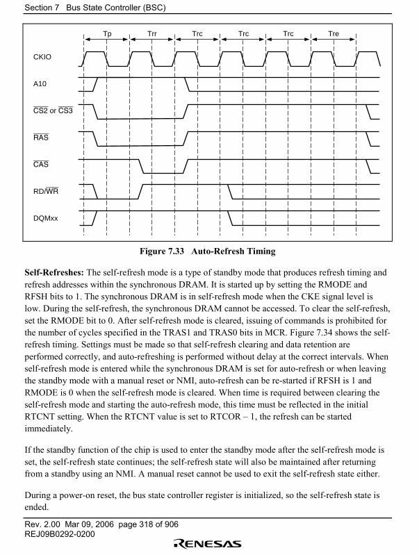
Section 7 Bus State Controller (BSC)
Rev. 2.00 Mar 09, 2006 page 318 of 906REJ09B0292-0200
Tp Trr
CKIO
A10
CS2 or CS3
RAS
CAS
RD/WR
DQMxx
Trc Trc Trc Tre
Figure 7.33 Auto-Refresh Timing
Self-Refreshes: The self-refresh mode is a type of standby mode that produces refresh timing andrefresh addresses within the synchronous DRAM. It is started up by setting the RMODE andRFSH bits to 1. The synchronous DRAM is in self-refresh mode when the CKE signal level islow. During the self-refresh, the synchronous DRAM cannot be accessed. To clear the self-refresh,set the RMODE bit to 0. After self-refresh mode is cleared, issuing of commands is prohibited forthe number of cycles specified in the TRAS1 and TRAS0 bits in MCR. Figure 7.34 shows the self-refresh timing. Settings must be made so that self-refresh clearing and data retention areperformed correctly, and auto-refreshing is performed without delay at the correct intervals. Whenself-refresh mode is entered while the synchronous DRAM is set for auto-refresh or when leavingthe standby mode with a manual reset or NMI, auto-refresh can be re-started if RFSH is 1 andRMODE is 0 when the self-refresh mode is cleared. When time is required between clearing theself-refresh mode and starting the auto-refresh mode, this time must be reflected in the initialRTCNT setting. When the RTCNT value is set to RTCOR � 1, the refresh can be startedimmediately.
If the standby function of the chip is used to enter the standby mode after the self-refresh mode isset, the self-refresh state continues; the self-refresh state will also be maintained after returningfrom a standby using an NMI. A manual reset cannot be used to exit the self-refresh state either.
During a power-on reset, the bus state controller register is initialized, so the self-refresh state isended.
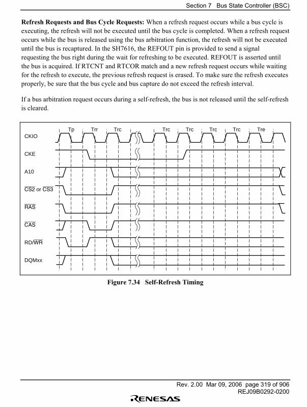
Section 7 Bus State Controller (BSC)
Rev. 2.00 Mar 09, 2006 page 319 of 906REJ09B0292-0200
Refresh Requests and Bus Cycle Requests: When a refresh request occurs while a bus cycle isexecuting, the refresh will not be executed until the bus cycle is completed. When a refresh requestoccurs while the bus is released using the bus arbitration function, the refresh will not be executeduntil the bus is recaptured. In the SH7616, the REFOUT pin is provided to send a signalrequesting the bus right during the wait for refreshing to be executed. REFOUT is asserted untilthe bus is acquired. If RTCNT and RTCOR match and a new refresh request occurs while waitingfor the refresh to execute, the previous refresh request is erased. To make sure the refresh executesproperly, be sure that the bus cycle and bus capture do not exceed the refresh interval.
If a bus arbitration request occurs during a self-refresh, the bus is not released until the self-refreshis cleared.
TpCKIO
CKE
A10
CS2 or CS3
RAS
CAS
RD/WR
DQMxx
Trr Trc Trc Trc Trc Trc Tre
Figure 7.34 Self-Refresh Timing
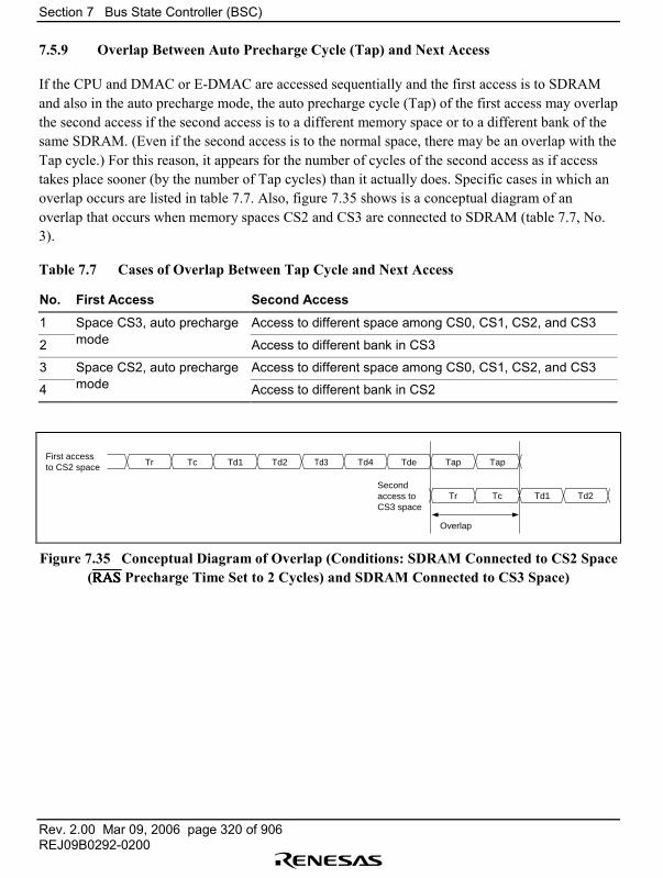
Section 7 Bus State Controller (BSC)
Rev. 2.00 Mar 09, 2006 page 320 of 906REJ09B0292-0200
7.5.9 Overlap Between Auto Precharge Cycle (Tap) and Next Access
If the CPU and DMAC or E-DMAC are accessed sequentially and the first access is to SDRAMand also in the auto precharge mode, the auto precharge cycle (Tap) of the first access may overlapthe second access if the second access is to a different memory space or to a different bank of thesame SDRAM. (Even if the second access is to the normal space, there may be an overlap with theTap cycle.) For this reason, it appears for the number of cycles of the second access as if accesstakes place sooner (by the number of Tap cycles) than it actually does. Specific cases in which anoverlap occurs are listed in table 7.7. Also, figure 7.35 shows is a conceptual diagram of anoverlap that occurs when memory spaces CS2 and CS3 are connected to SDRAM (table 7.7, No.3).
Table 7.7 Cases of Overlap Between Tap Cycle and Next Access
No. First Access Second Access
1 Space CS3, auto precharge Access to different space among CS0, CS1, CS2, and CS3
2 mode Access to different bank in CS3
3 Space CS2, auto precharge Access to different space among CS0, CS1, CS2, and CS3
4 mode Access to different bank in CS2
First accessto CS2 space Tr Tc Td1 Td2 Td4 Tde Tap TapTd3
Tr Tc Td1 Td2
Overlap
Secondaccess toCS3 space
Figure 7.35 Conceptual Diagram of Overlap (Conditions: SDRAM Connected to CS2 Space(RASRASRASRAS Precharge Time Set to 2 Cycles) and SDRAM Connected to CS3 Space)
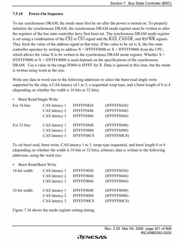
Section 7 Bus State Controller (BSC)
Rev. 2.00 Mar 09, 2006 page 321 of 906REJ09B0292-0200
7.5.10 Power-On Sequence
To use synchronous DRAM, the mode must first be set after the power is turned on. To properlyinitialize the synchronous DRAM, the synchronous DRAM mode register must be written to afterthe registers of the bus state controller have first been set. The synchronous DRAM mode registeris set using a combination of the CS2 or CS3 signal and the RAS, CAS/OE, and RD/WR signals.They fetch the value of the address signal at that time. If the value to be set is X, the bus statecontroller operates by writing to address X + H'FFFF0000 or X + H'FFFF8000 from the CPU,which allows the value X to be written to the synchronous DRAM mode register. Whether X +H'FFFF0000 or X + H'FFFF8000 is used depends on the specifications of the synchronousDRAM. Use a value in the range H'000 to H'FFF for X. Data is ignored at this time, but the modeis written using word as the size.
Write any data in word size to the following addresses to select the burst read single writesupported by the chip, a CAS latency of 1 to 3, a sequential wrap type, and a burst length of 8 or 4(depending on whether the width is 16 bits or 32 bits).
• Burst Read/Single WriteFor 16 bits: CAS latency 1
CAS latency 2CAS latency 3
H'FFFF0426H'FFFF0446H'FFFF0466
(H'FFFF8426)(H'FFFF8446)(H'FFFF8466)
For 32 bits: CAS latency 1CAS latency 2CAS latency 3
H'FFFF0848H'FFFF0888H'FFFF08C8
(H'FFFF8848)(H'FFFF8888)(H'FFFF88C8)
To set burst read, burst write, CAS latency 1 to 3, wrap-type sequential, and burst length 8 or 4(depending on whether the width is 16 bits or 32 bits), arbitrary data is written to the followingaddresses, using the word size.
• Burst Read/Burst Write16-bit width: CAS latency 1
CAS latency 2CAS latency 3
H'FFFF0026H'FFFF0046H'FFFF0066
(H'FFFF8026)(H'FFFF8046)(H'FFFF8066)
32-bit width: CAS latency 1CAS latency 2CAS latency 3
H'FFFF0048H'FFFF0088H'FFFF00C8
(H'FFFF8048)(H'FFFF8088)(H'FFFF80C8)
Figure 7.36 shows the mode register setting timing.
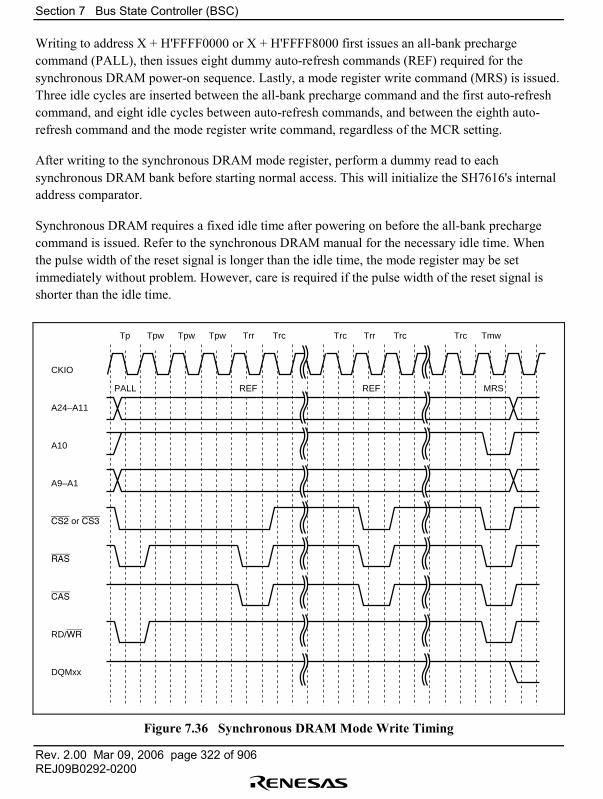
Section 7 Bus State Controller (BSC)
Rev. 2.00 Mar 09, 2006 page 322 of 906REJ09B0292-0200
Writing to address X + H'FFFF0000 or X + H'FFFF8000 first issues an all-bank prechargecommand (PALL), then issues eight dummy auto-refresh commands (REF) required for thesynchronous DRAM power-on sequence. Lastly, a mode register write command (MRS) is issued.Three idle cycles are inserted between the all-bank precharge command and the first auto-refreshcommand, and eight idle cycles between auto-refresh commands, and between the eighth auto-refresh command and the mode register write command, regardless of the MCR setting.
After writing to the synchronous DRAM mode register, perform a dummy read to eachsynchronous DRAM bank before starting normal access. This will initialize the SH7616's internaladdress comparator.
Synchronous DRAM requires a fixed idle time after powering on before the all-bank prechargecommand is issued. Refer to the synchronous DRAM manual for the necessary idle time. Whenthe pulse width of the reset signal is longer than the idle time, the mode register may be setimmediately without problem. However, care is required if the pulse width of the reset signal isshorter than the idle time.
Tp Tpw Tpw Tpw Trr Trc Trc Trr Trc Trc Tmw
CKIO
A24–A11
A10
A9–A1
CS2 or CS3
RAS
CAS
RD/WR
DQMxx
MRSREFREFPALL
Figure 7.36 Synchronous DRAM Mode Write Timing
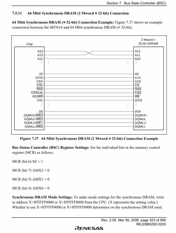
Section 7 Bus State Controller (BSC)
Rev. 2.00 Mar 09, 2006 page 323 of 906REJ09B0292-0200
7.5.11 64 Mbit Synchronous DRAM (2 Mword ×××× 32-bit) Connection
64 Mbit Synchronous DRAM (×××× 32-bit) Connection Example: Figure 7.37 shows an exampleconnection between the SH7616 and 64 Mbit synchronous DRAM (× 32-bit).
A22A13A12
A2CKIOCKECSn
RAS
CAS/OERD/WR
D31
D0DQMUU/WE3
DQMUL/WE2
DQMLU/WE1
DQMLL/WE0
Chip2 Mword ×
32-bit SDRAM
A12A11A10 A0CLKCKECS
RAS
CAS
WE
I/O31
I/O0DQMUUDQMULDQMLUDQMLL
Figure 7.37 64 Mbit Synchronous DRAM (2 Mword ×××× 32-bit) Connection Example
Bus Status Controller (BSC) Register Settings: Set the individual bits in the memory controlregister (MCR) as follows.
MCR (bit 6) SZ = 1
MCR (bit 7) AMX2 = 0
MCR (bit 5) AMX1 = 0
MCR (bit 4) AMX0 = 0
Synchronous DRAM Mode Settings: To make mode settings for the synchronous DRAM, writeto address X+H'FFFF0000 or X+H'FFFF8000 from the CPU. (X represents the setting value.)Whether to use X+H'FFFF0000 or X+H'FFFF8000 determines on the synchronous DRAM used.
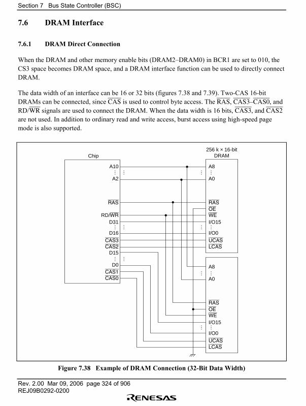
Section 7 Bus State Controller (BSC)
Rev. 2.00 Mar 09, 2006 page 324 of 906REJ09B0292-0200
7.6 DRAM Interface
7.6.1 DRAM Direct Connection
When the DRAM and other memory enable bits (DRAM2�DRAM0) in BCR1 are set to 010, theCS3 space becomes DRAM space, and a DRAM interface function can be used to directly connectDRAM.
The data width of an interface can be 16 or 32 bits (figures 7.38 and 7.39). Two-CAS 16-bitDRAMs can be connected, since CAS is used to control byte access. The RAS, CAS3�CAS0, andRD/WR signals are used to connect the DRAM. When the data width is 16 bits, CAS3, and CAS2are not used. In addition to ordinary read and write access, burst access using high-speed pagemode is also supported.
A10
A2
D15
D0
RAS
RD/WR
D31
D16CAS3
CAS2
A8
A0
RAS
OE
WE
I/O15
I/O0UCAS
LCAS
CAS1
CAS0
A8
A0
RAS
OE
WE
I/O15
I/O0UCAS
LCAS
Chip256 k × 16-bit
DRAM
……
……
… …
……
…
…
………
…
Figure 7.38 Example of DRAM Connection (32-Bit Data Width)
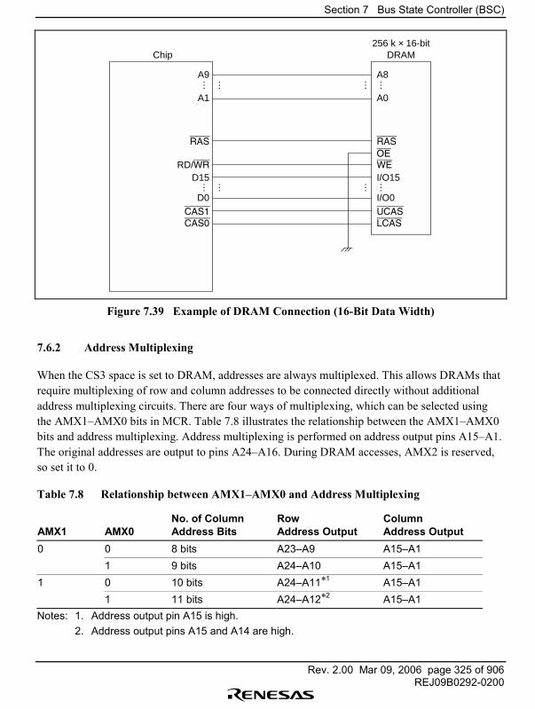
Section 7 Bus State Controller (BSC)
Rev. 2.00 Mar 09, 2006 page 325 of 906REJ09B0292-0200
A9
A1
RAS
RD/WR
D15
D0CAS1
CAS0
A8
A0
RAS
OE
WE
I/O15
I/O0UCAS
LCAS
Chip256 k × 16-bit
DRAM
……
……
……
……
Figure 7.39 Example of DRAM Connection (16-Bit Data Width)
7.6.2 Address Multiplexing
When the CS3 space is set to DRAM, addresses are always multiplexed. This allows DRAMs thatrequire multiplexing of row and column addresses to be connected directly without additionaladdress multiplexing circuits. There are four ways of multiplexing, which can be selected usingthe AMX1�AMX0 bits in MCR. Table 7.8 illustrates the relationship between the AMX1�AMX0bits and address multiplexing. Address multiplexing is performed on address output pins A15�A1.The original addresses are output to pins A24�A16. During DRAM accesses, AMX2 is reserved,so set it to 0.
Table 7.8 Relationship between AMX1�AMX0 and Address Multiplexing
AMX1 AMX0No. of ColumnAddress Bits
RowAddress Output
ColumnAddress Output
0 0 8 bits A23�A9 A15�A11 9 bits A24�A10 A15�A1
1 0 10 bits A24�A11*1 A15�A11 11 bits A24�A12*2 A15�A1
Notes: 1. Address output pin A15 is high.2. Address output pins A15 and A14 are high.
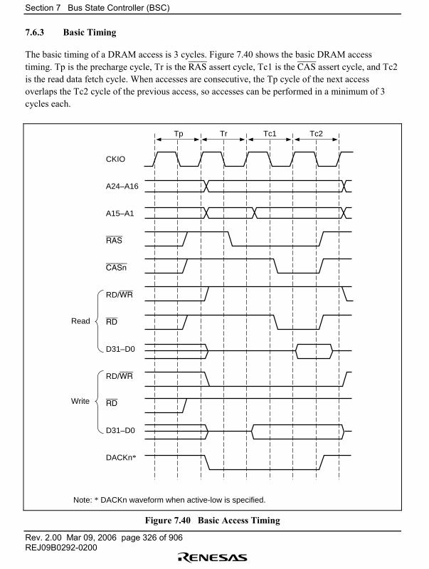
Section 7 Bus State Controller (BSC)
Rev. 2.00 Mar 09, 2006 page 326 of 906REJ09B0292-0200
7.6.3 Basic Timing
The basic timing of a DRAM access is 3 cycles. Figure 7.40 shows the basic DRAM accesstiming. Tp is the precharge cycle, Tr is the RAS assert cycle, Tc1 is the CAS assert cycle, and Tc2is the read data fetch cycle. When accesses are consecutive, the Tp cycle of the next accessoverlaps the Tc2 cycle of the previous access, so accesses can be performed in a minimum of 3cycles each.
Tp Tr
CKIO
A24–A16
A15–A1
RAS
CASn
RD/WR
RD
D31–D0
RD/WR
RD
D31–D0
DACKn*
Read
Write
Tc1 Tc2
Note: * DACKn waveform when active-low is specified.
Figure 7.40 Basic Access Timing
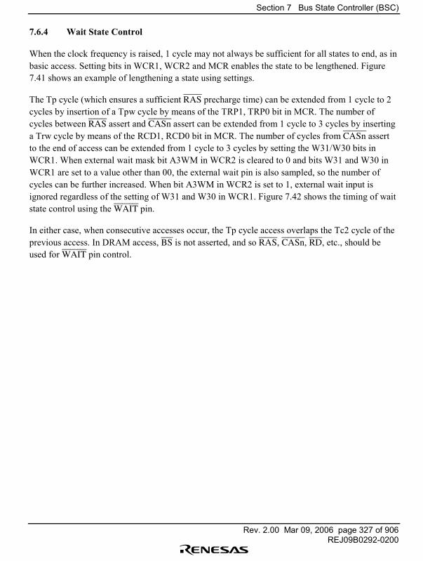
Section 7 Bus State Controller (BSC)
Rev. 2.00 Mar 09, 2006 page 327 of 906REJ09B0292-0200
7.6.4 Wait State Control
When the clock frequency is raised, 1 cycle may not always be sufficient for all states to end, as inbasic access. Setting bits in WCR1, WCR2 and MCR enables the state to be lengthened. Figure7.41 shows an example of lengthening a state using settings.
The Tp cycle (which ensures a sufficient RAS precharge time) can be extended from 1 cycle to 2cycles by insertion of a Tpw cycle by means of the TRP1, TRP0 bit in MCR. The number ofcycles between RAS assert and CASn assert can be extended from 1 cycle to 3 cycles by insertinga Trw cycle by means of the RCD1, RCD0 bit in MCR. The number of cycles from CASn assertto the end of access can be extended from 1 cycle to 3 cycles by setting the W31/W30 bits inWCR1. When external wait mask bit A3WM in WCR2 is cleared to 0 and bits W31 and W30 inWCR1 are set to a value other than 00, the external wait pin is also sampled, so the number ofcycles can be further increased. When bit A3WM in WCR2 is set to 1, external wait input isignored regardless of the setting of W31 and W30 in WCR1. Figure 7.42 shows the timing of waitstate control using the WAIT pin.
In either case, when consecutive accesses occur, the Tp cycle access overlaps the Tc2 cycle of theprevious access. In DRAM access, BS is not asserted, and so RAS, CASn, RD, etc., should beused for WAIT pin control.
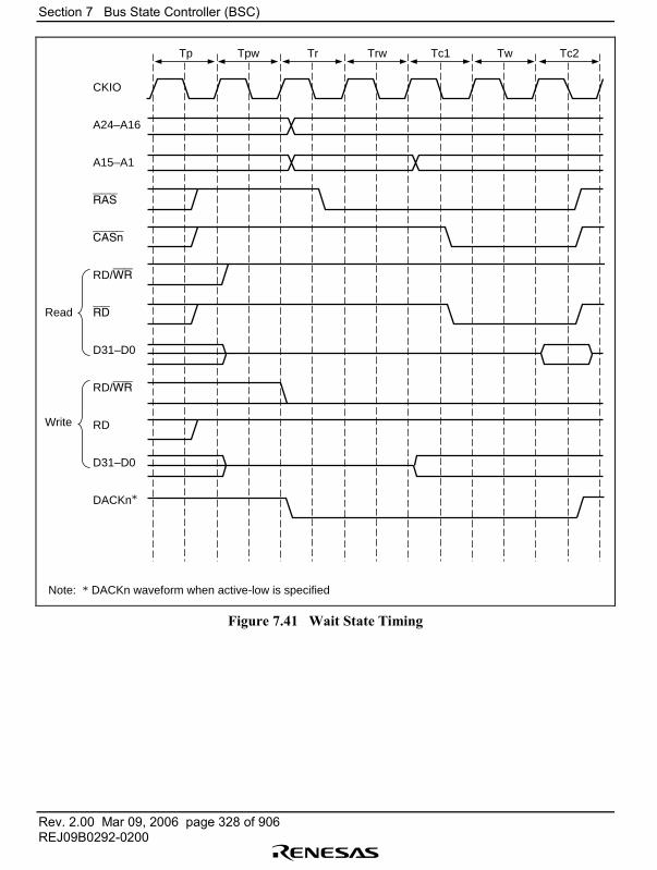
Section 7 Bus State Controller (BSC)
Rev. 2.00 Mar 09, 2006 page 328 of 906REJ09B0292-0200
Tp Tpw
CKIO
A24–A16
A15–A1
RAS
CASn
RD/WR
RD
D31–D0
RD/WR
RD
D31–D0
DACKn*
Read
Write
Note: * DACKn waveform when active-low is specified
Tr Trw Tc1 Tw Tc2
Figure 7.41 Wait State Timing
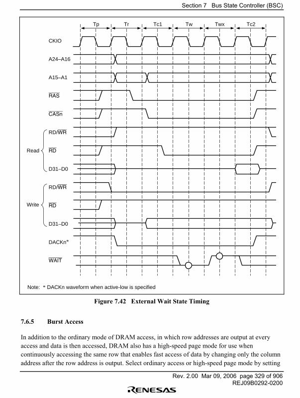
Section 7 Bus State Controller (BSC)
Rev. 2.00 Mar 09, 2006 page 329 of 906REJ09B0292-0200
Tp Tr
CKIO
A24–A16
A15–A1
RAS
CASn
RD/WR
RD
D31–D0
RD/WR
RD
D31–D0
DACKn*
WAIT
Read
Write
Tc1 Tw Twx Tc2
Note: * DACKn waveform when active-low is specified
Figure 7.42 External Wait State Timing
7.6.5 Burst Access
In addition to the ordinary mode of DRAM access, in which row addresses are output at everyaccess and data is then accessed, DRAM also has a high-speed page mode for use whencontinuously accessing the same row that enables fast access of data by changing only the columnaddress after the row address is output. Select ordinary access or high-speed page mode by setting
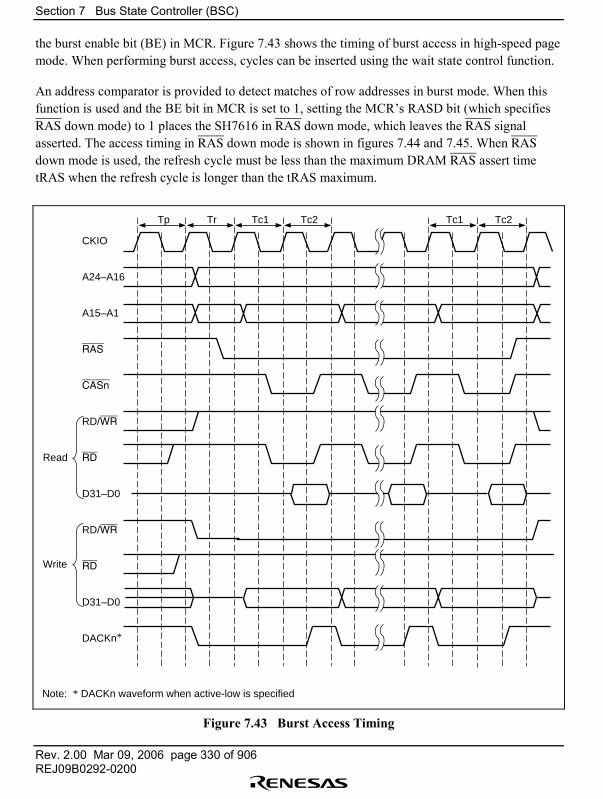
Section 7 Bus State Controller (BSC)
Rev. 2.00 Mar 09, 2006 page 330 of 906REJ09B0292-0200
the burst enable bit (BE) in MCR. Figure 7.43 shows the timing of burst access in high-speed pagemode. When performing burst access, cycles can be inserted using the wait state control function.
An address comparator is provided to detect matches of row addresses in burst mode. When thisfunction is used and the BE bit in MCR is set to 1, setting the MCR�s RASD bit (which specifiesRAS down mode) to 1 places the SH7616 in RAS down mode, which leaves the RAS signalasserted. The access timing in RAS down mode is shown in figures 7.44 and 7.45. When RASdown mode is used, the refresh cycle must be less than the maximum DRAM RAS assert timetRAS when the refresh cycle is longer than the tRAS maximum.
Tp
CKIO
A24–A16
A15–A1
RAS
CASn
RD/WR
RD
D31–D0
RD/WR
RD
D31–D0
DACKn*
Read
Write
Tr Tc1 Tc2 Tc1 Tc2
Note: * DACKn waveform when active-low is specified
Figure 7.43 Burst Access Timing
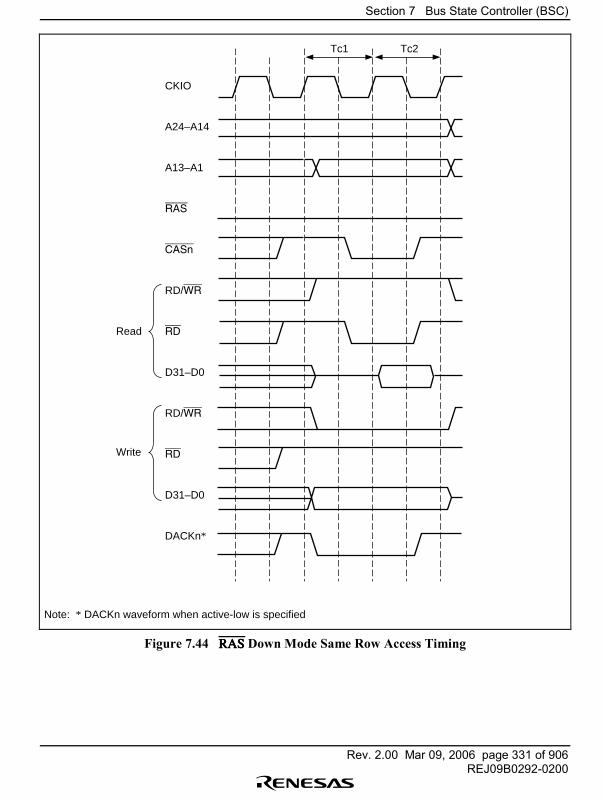
Section 7 Bus State Controller (BSC)
Rev. 2.00 Mar 09, 2006 page 331 of 906REJ09B0292-0200
CKIO
A24–A14
A13–A1
RAS
CASn
RD/WR
RD
D31–D0
RD/WR
RD
D31–D0
DACKn*
Read
Write
Tc1 Tc2
Note: * DACKn waveform when active-low is specified
Figure 7.44 RASRASRASRAS Down Mode Same Row Access Timing
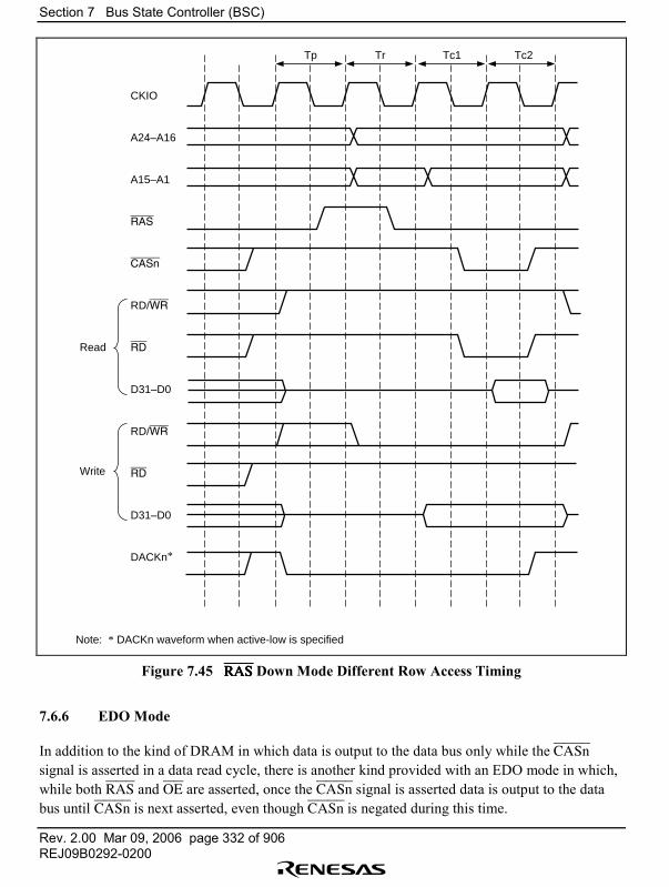
Section 7 Bus State Controller (BSC)
Rev. 2.00 Mar 09, 2006 page 332 of 906REJ09B0292-0200
Tp Tr
CKIO
A24–A16
A15–A1
RAS
CASn
RD/WR
RD
D31–D0
RD/WR
RD
D31–D0
DACKn*
Read
Write
Tc1 Tc2
Note: * DACKn waveform when active-low is specified
Figure 7.45 RASRASRASRAS Down Mode Different Row Access Timing
7.6.6 EDO Mode
In addition to the kind of DRAM in which data is output to the data bus only while the CASnsignal is asserted in a data read cycle, there is another kind provided with an EDO mode in which,while both RAS and OE are asserted, once the CASn signal is asserted data is output to the databus until CASn is next asserted, even though CASn is negated during this time.
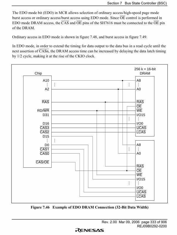
Section 7 Bus State Controller (BSC)
Rev. 2.00 Mar 09, 2006 page 333 of 906REJ09B0292-0200
The EDO mode bit (EDO) in MCR allows selection of ordinary access/high-speed page modeburst access or ordinary access/burst access using EDO mode. Since OE control is performed inEDO mode DRAM access, the CAS and OE pins of the SH7616 must be connected to the OE pinof the DRAM.
Ordinary access in EDO mode is shown in figure 7.48, and burst access in figure 7.49.
In EDO mode, in order to extend the timing for data output to the data bus in a read cycle until thenext assertion of CASn, the DRAM access time can be increased by delaying the data latch timingby 1/2 cycle, making it at the rise of the CKIO clock.
A8
A0
RAS
OE
WE
I/O15
I/O0UCAS
LCAS
A8
A0
RAS
OE
WE
I/O15
I/O0UCAS
LCAS
A10
A2
RAS
RD/WR
D31
D16CAS3
CAS2
D15
D0CAS1
CAS0
CAS/OE
........
........
........
........
........
........
256 k × 16-bitDRAMChip
Figure 7.46 Example of EDO DRAM Connection (32-Bit Data Width)
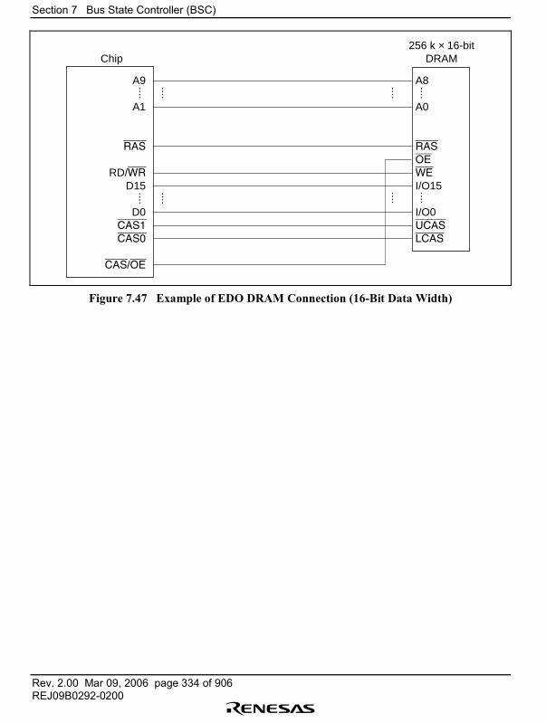
Section 7 Bus State Controller (BSC)
Rev. 2.00 Mar 09, 2006 page 334 of 906REJ09B0292-0200
A8
A0
RAS
OE
WE
I/O15
I/O0UCAS
LCAS
A9
A1
RAS
RD/WR
D15
D0CAS1
CAS0
CAS/OE
........
........
........
........
256 k × 16-bitDRAMChip
Figure 7.47 Example of EDO DRAM Connection (16-Bit Data Width)
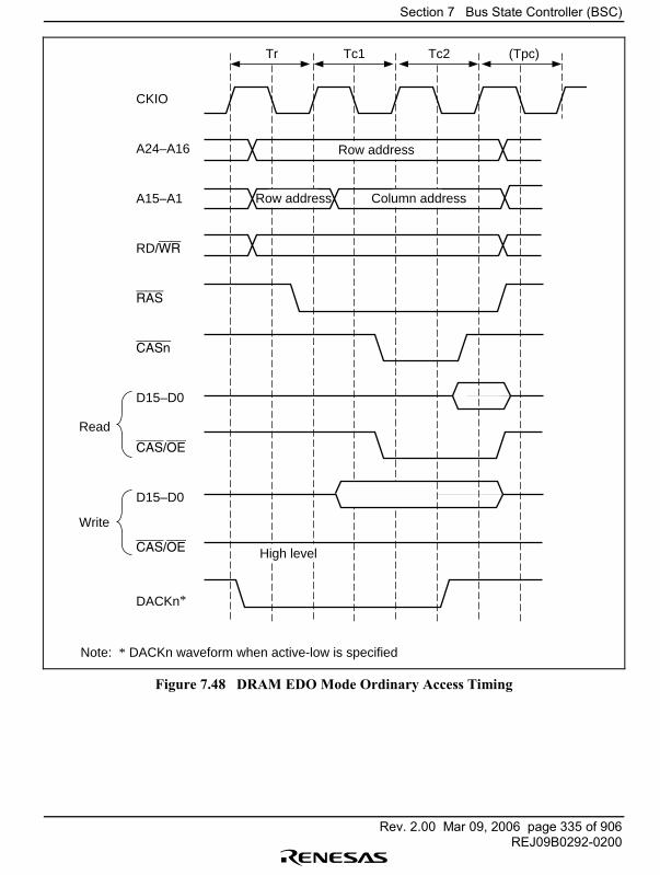
Section 7 Bus State Controller (BSC)
Rev. 2.00 Mar 09, 2006 page 335 of 906REJ09B0292-0200
Tr Tc1
CKIO
A24–A16
A15–A1
RD/WR
RAS
CASn
D15–D0
CAS/OE
D15–D0
CAS/OE
DACKn*
Read
Note: * DACKn waveform when active-low is specified
Write
Tc2 (Tpc)
Row address
Column addressRow address
High level
Figure 7.48 DRAM EDO Mode Ordinary Access Timing
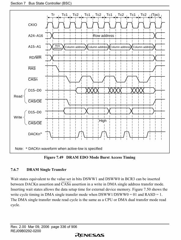
Section 7 Bus State Controller (BSC)
Rev. 2.00 Mar 09, 2006 page 336 of 906REJ09B0292-0200
Tr
CKIO
A24–A16
A15–A1
RD/WR
RAS
CASn
D15–D0
CAS/OE
D15–D0
CAS/OE
DACKn*
Tc1 Tc2 Tc1 Tc2 Tc1 Tc2 Tc1 Tc2 (Tpc)
Read
Note: * DACKn waveform when active-low is specified
Write
Column addressColumn addressColumn addressColumn addressRowaddress
Row address
High
Figure 7.49 DRAM EDO Mode Burst Access Timing
7.6.7 DRAM Single Transfer
Wait states equivalent to the value set in bits DSWW1 and DSWW0 in BCR3 can be insertedbetween DACKn assertion and CASn assertion in a write in DMA single address transfer mode.Inserting wait states allows the data setup time for external device memory. Figure 7.50 shows thewrite cycle timing in DMA single transfer mode when DSWW1/DSWW0 = 01 and RASD = 1.The DMA single transfer mode read cycle is the same as a CPU or DMA dual transfer mode readcycle.

Section 7 Bus State Controller (BSC)
Rev. 2.00 Mar 09, 2006 page 337 of 906REJ09B0292-0200
Tdsww Tc1
CKIO
A24–A16
A15–A1
RAS
CASn
RD/WR
D31–D0
DACKn*
Tc2
Low level
Note: * DACKn waveform when active-low is specified
Figure 7.50 DMA Single Transfer Mode Write Cycle Timing(RASRASRASRAS Down Mode, Same Row Address)
7.6.8 Refreshing
The bus state controller includes a function for controlling DRAM refreshing. Distributedrefreshing using a CAS-before-RAS refresh cycle can be performed by clearing the RMODE bit to0 and setting the RFSH bit to 1 in MCR. Consecutive refreshes can be generated by setting bitsRRC2�RRC0 in RTCSR. If DRAM is not accessed for a long period, self-refresh mode, whichuses little power consumption for data retention, can be activated by setting both the RMODE andRFSH bits to 1.
CASCASCASCAS-Before-RASRASRASRAS Refreshing: Refreshing is performed at intervals determined by the input clockselected by bits CKS2�CKS0 in RTCSR, and the value set in RTCOR. The RTCOR value and thevalue of bits CKS2�CKS0 in RTCSR should be set so as to satisfy the refresh interval
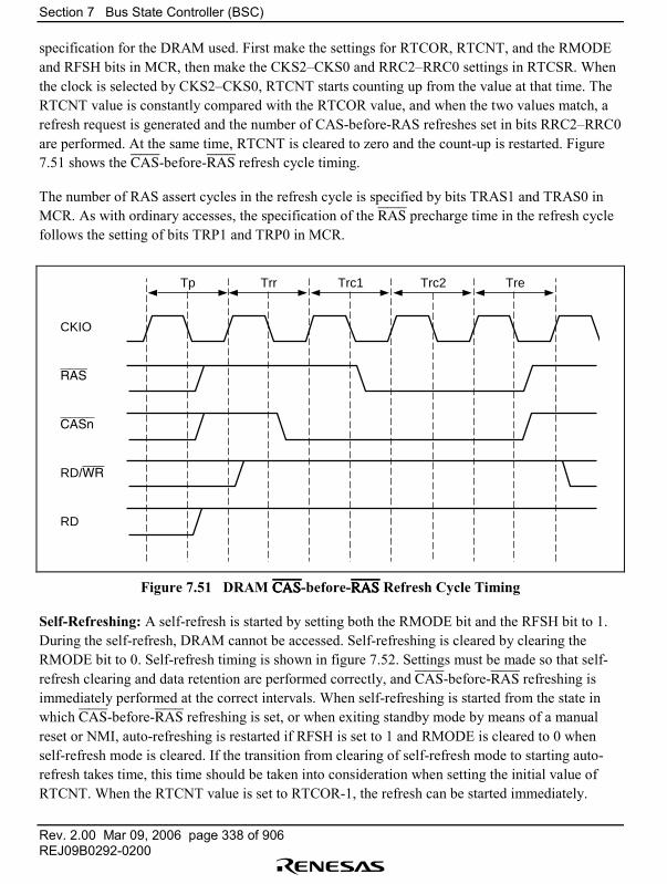
Section 7 Bus State Controller (BSC)
Rev. 2.00 Mar 09, 2006 page 338 of 906REJ09B0292-0200
specification for the DRAM used. First make the settings for RTCOR, RTCNT, and the RMODEand RFSH bits in MCR, then make the CKS2�CKS0 and RRC2�RRC0 settings in RTCSR. Whenthe clock is selected by CKS2�CKS0, RTCNT starts counting up from the value at that time. TheRTCNT value is constantly compared with the RTCOR value, and when the two values match, arefresh request is generated and the number of CAS-before-RAS refreshes set in bits RRC2�RRC0are performed. At the same time, RTCNT is cleared to zero and the count-up is restarted. Figure7.51 shows the CAS-before-RAS refresh cycle timing.
The number of RAS assert cycles in the refresh cycle is specified by bits TRAS1 and TRAS0 inMCR. As with ordinary accesses, the specification of the RAS precharge time in the refresh cyclefollows the setting of bits TRP1 and TRP0 in MCR.
Tp Trr
CKIO
RAS
CASn
RD/WR
RD
Trc1 Trc2 Tre
Figure 7.51 DRAM CASCASCASCAS-before-RASRASRASRAS Refresh Cycle Timing
Self-Refreshing: A self-refresh is started by setting both the RMODE bit and the RFSH bit to 1.During the self-refresh, DRAM cannot be accessed. Self-refreshing is cleared by clearing theRMODE bit to 0. Self-refresh timing is shown in figure 7.52. Settings must be made so that self-refresh clearing and data retention are performed correctly, and CAS-before-RAS refreshing isimmediately performed at the correct intervals. When self-refreshing is started from the state inwhich CAS-before-RAS refreshing is set, or when exiting standby mode by means of a manualreset or NMI, auto-refreshing is restarted if RFSH is set to 1 and RMODE is cleared to 0 whenself-refresh mode is cleared. If the transition from clearing of self-refresh mode to starting auto-refresh takes time, this time should be taken into consideration when setting the initial value ofRTCNT. When the RTCNT value is set to RTCOR-1, the refresh can be started immediately.
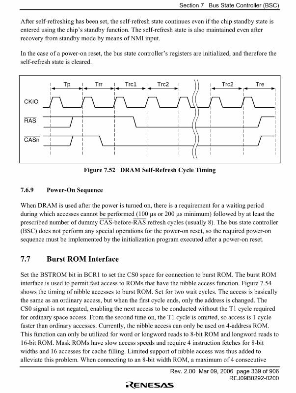
Section 7 Bus State Controller (BSC)
Rev. 2.00 Mar 09, 2006 page 339 of 906REJ09B0292-0200
After self-refreshing has been set, the self-refresh state continues even if the chip standby state isentered using the chip�s standby function. The self-refresh state is also maintained even afterrecovery from standby mode by means of NMI input.
In the case of a power-on reset, the bus state controller�s registers are initialized, and therefore theself-refresh state is cleared.
Tp Trr
CKIO
RAS
CASn
Trc1 Trc2 Trc2 Tre
Figure 7.52 DRAM Self-Refresh Cycle Timing
7.6.9 Power-On Sequence
When DRAM is used after the power is turned on, there is a requirement for a waiting periodduring which accesses cannot be performed (100 µs or 200 µs minimum) followed by at least theprescribed number of dummy CAS-before-RAS refresh cycles (usually 8). The bus state controller(BSC) does not perform any special operations for the power-on reset, so the required power-onsequence must be implemented by the initialization program executed after a power-on reset.
7.7 Burst ROM Interface
Set the BSTROM bit in BCR1 to set the CS0 space for connection to burst ROM. The burst ROMinterface is used to permit fast access to ROMs that have the nibble access function. Figure 7.54shows the timing of nibble accesses to burst ROM. Set for two wait cycles. The access is basicallythe same as an ordinary access, but when the first cycle ends, only the address is changed. TheCS0 signal is not negated, enabling the next access to be conducted without the T1 cycle requiredfor ordinary space access. From the second time on, the T1 cycle is omitted, so access is 1 cyclefaster than ordinary accesses. Currently, the nibble access can only be used on 4-address ROM.This function can only be utilized for word or longword reads to 8-bit ROM and longword reads to16-bit ROM. Mask ROMs have slow access speeds and require 4 instruction fetches for 8-bitwidths and 16 accesses for cache filling. Limited support of nibble access was thus added toalleviate this problem. When connecting to an 8-bit width ROM, a maximum of 4 consecutive
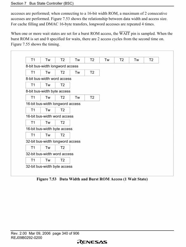
Section 7 Bus State Controller (BSC)
Rev. 2.00 Mar 09, 2006 page 340 of 906REJ09B0292-0200
accesses are performed; when connecting to a 16-bit width ROM, a maximum of 2 consecutiveaccesses are performed. Figure 7.53 shows the relationship between data width and access size.For cache filling and DMAC 16-byte transfers, longword accesses are repeated 4 times.
When one or more wait states are set for a burst ROM access, the WAIT pin is sampled. When theburst ROM is set and 0 specified for waits, there are 2 access cycles from the second time on.Figure 7.55 shows the timing.
T1 Tw T2 Tw T2 Tw T2 Tw T2
8-bit bus-width longword access
T1 Tw T2 Tw T2
8-bit bus-width word access
T1 Tw T2
8-bit bus-width byte access
T1 Tw T2 Tw T2
16-bit bus-width longword access
T1 Tw T2
16-bit bus-width word access
T1 Tw T2
16-bit bus-width byte access
T1 Tw T2
32-bit bus-width longword access
T1 Tw T2
32-bit bus-width word access
T1 Tw T2
32-bit bus-width byte access
Figure 7.53 Data Width and Burst ROM Access (1 Wait State)
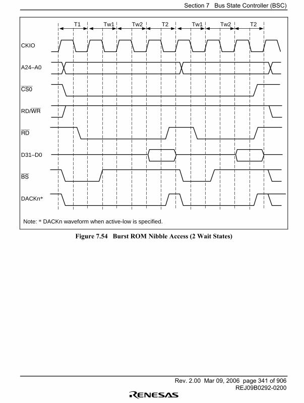
Section 7 Bus State Controller (BSC)
Rev. 2.00 Mar 09, 2006 page 341 of 906REJ09B0292-0200
T1 Tw1
CKIO
A24–A0
CS0
RD/WR
RD
D31–D0
BS
DACKn*
Tw2 T2 Tw1 Tw2 T2
Note: * DACKn waveform when active-low is specified.
Figure 7.54 Burst ROM Nibble Access (2 Wait States)
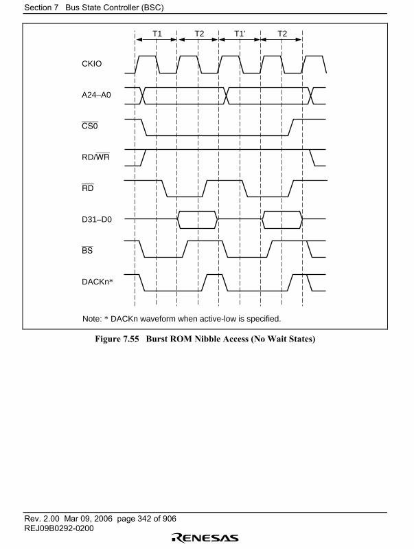
Section 7 Bus State Controller (BSC)
Rev. 2.00 Mar 09, 2006 page 342 of 906REJ09B0292-0200
T1 T2
CKIO
A24–A0
CS0
RD/WR
RD
D31–D0
BS
DACKn*
T1' T2
Note: * DACKn waveform when active-low is specified.
Figure 7.55 Burst ROM Nibble Access (No Wait States)
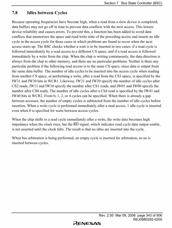
Section 7 Bus State Controller (BSC)
Rev. 2.00 Mar 09, 2006 page 343 of 906REJ09B0292-0200
7.8 Idles between Cycles
Because operating frequencies have become high, when a read from a slow device is completed,data buffers may not go off in time to prevent data conflicts with the next access. This lowersdevice reliability and causes errors. To prevent this, a function has been added to avoid dataconflicts that memorizes the space and read/write state of the preceding access and inserts an idlecycle in the access cycle for those cases in which problems are found to occur when the nextaccess starts up. The BSC checks whether a wait is to be inserted in two cases: if a read cycle isfollowed immediately by a read access to a different CS space, and if a read access is followedimmediately by a write from the chip. When the chip is writing continuously, the data direction isalways from the chip to other memory, and there are no particular problems. Neither is there anyparticular problem if the following read access is to the same CS space, since data is output fromthe same data buffer. The number of idle cycles to be inserted into the access cycle when readingfrom another CS space, or performing a write, after a read from the CS3 space, is specified by theIW31 and IW30 bits in WCR1. Likewise, IW21 and IW20 specify the number of idle cycles afterCS2 reads, IW11 and IW10 specify the number after CS1 reads, and IW01 and IW00 specify thenumber after CS0 reads. The number of idle cycles after a CS4 read is specified by the IW41 andIW40 bits in WCR2. From 0, 1, 2, or 4 cycles can be specified. When there is already a gapbetween accesses, the number of empty cycles is subtracted from the number of idle cycles beforeinsertion. When a write cycle is performed immediately after a read access, 1 idle cycle is insertedeven when 0 is specified for waits between access cycles.
When the chip shifts to a read cycle immediately after a write, the write data becomes highimpedance when the clock rises, but the RD signal, which indicates read cycle data output enable,is not asserted until the clock falls. The result is that no idles are inserted into the cycle.
When bus arbitration is being performed, an empty cycle is inserted for arbitration, so no isinserted between cycles.
Section 7 Bus State Controller (BSC)
Rev. 2.00 Mar 09, 2006 page 344 of 906REJ09B0292-0200
T1 T2
CKIO
A24–A0
CSm
CSn
BS
RD/WR
RD
D31–D0
Twait T1 T2 Twait T1 T2
CSm space read CSn space read CSn space write
Specification of waitsbetween CSm accesses
(reading different spaces)
Specification of waitsbetween CSn accesses(read followed by write)
Figure 7.56 Idles between Cycles
Section 7 Bus State Controller (BSC)
Rev. 2.00 Mar 09, 2006 page 345 of 906REJ09B0292-0200
7.9 Bus Arbitration
The chip has a bus arbitration function that, when a bus release request is received from anexternal device, releases the bus to that device after the bus cycle being executed is completed.
The chip keeps the bus under normal conditions and permits other devices to use the bus byreleasing it when they request its use.
In the following explanation, external devices requesting the bus are called slaves.
The chip has three internal bus masters, the CPU, the DMAC and the E-DMAC. Whensynchronous DRAM or DRAM is connected and refresh control is performed, the refresh requestbecomes a fourth master. In addition to these, there are also bus requests from external devices.The priority for bus requests when they occur simultaneously is as follows.
Refresh request External device E-DMAC DMAC CPU
However, only one E-DMAC channel can hold the bus during one bus-mastership cycle.
The E-DMAC has two channels to handle both transmission and reception. Arbitration betweenthe channels is performed automatically within the E-DMAC module, with bus mastershipalternating between the transmit channel and the receive channel. For arbitration between the twoDMAC channels, either fixed priority mode or round robin mode can be selected by means of thepriority mode bit (PR) in the DMA operation register (DMAOR).
When the bus is being passed between slave and master, all bus control signals are negated beforethe bus is released to prevent erroneous operation of the connected devices. When the bus istransferred, also, the bus control signals begin bus driving from the negated state. The master andslave passing the bus between them drive the same signal values, so output buffer conflict isavoided. A pull-up resistance is required for the bus control signals to prevent malfunction causedby external noise when they are at high impedance.
Bus permission is granted at the end of the bus cycle. When the bus is requested, the bus isreleased immediately if there is no ongoing bus cycle. If there is a current bus cycle, the bus is notreleased until the bus cycle ends. Even when a bus cycle does not appear to be in progress whenviewed from off-chip, it is not possible to determine immediately whether the bus has beenreleased by looking at CSn or other control signals, since a bus cycle (such as wait insertionbetween access cycles) may have been started internally. The bus cannot be released during bursttransfers for cache filling, DMAC 16-byte block transfers (16 + 16 = 32-byte transfers in dualaddress mode), or E-DMAC 16-byte block transfers. Likewise, the bus cannot be released betweenthe read and write cycles of a TAS instruction. Arbitration is also not performed between multiple
Section 7 Bus State Controller (BSC)
Rev. 2.00 Mar 09, 2006 page 346 of 906REJ09B0292-0200
bus cycles produced by a data width smaller than the access size, such as a longword access to an8-bit data width memory. Bus arbitration is performed between external vector fetch, PC save, andSR save cycles during interrupt handling, which are all independent accesses.
Because the CPU is connected to cache memory by a dedicated internal bus, cache memory can beread even when the bus is being used by another bus master on the chip or externally. Whenwriting from the CPU, an external write cycle is produced. Since the internal bus that connects theCPU, DMAC, and on-chip peripheral modules can operate in parallel to the external bus, both readand write accesses from the CPU to on-chip peripheral modules and from the DMAC to on-chipperipheral modules are possible even if the external bus is not held.
Figures 7.57 (a) and 7.57 (b) show the timing charts in the cases that bus requests occursimultaneously from the E-DMAC, DMAC, and CPU. These cases are based on the followingsettings:
• The CS2 and CS3 spaces are set for synchronous DRAM.• The CAS latency is one cycle.• The E-DMAC is enabled at both the transmitter and receiver (the buffer and descriptor use the
CS3 space).• The DMAC is enabled in only one channel that is set to auto-request mode, cycle-steal mode,
and 16-byte dual-address transmission (CS2 space).• Burst read and single write are set to synchronous DRAM.
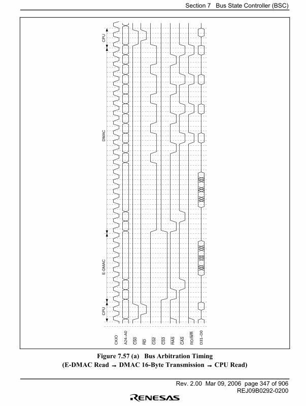
Section 7 Bus State Controller (BSC)
Rev. 2.00 Mar 09, 2006 page 347 of 906REJ09B0292-0200
CP
UD
MA
CE
-DM
AC
CP
U
CK
IO
A24
–A0
CS
0
RD
CS
2
CS
3
RA
S
CA
S
RD
/WR
D31
–D0
Figure 7.57 (a) Bus Arbitration Timing(E-DMAC Read →→→→ DMAC 16-Byte Transmission →→→→ CPU Read)
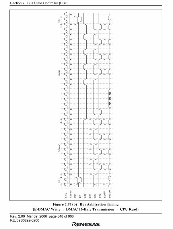
Section 7 Bus State Controller (BSC)
Rev. 2.00 Mar 09, 2006 page 348 of 906REJ09B0292-0200
CP
UD
MA
CE
-DM
AC
CP
U
CK
IO
A24
–A0
CS
0
RD
CS
2
CS
3
RA
S
CA
S
RD
/WR
D31
–D0
Figure 7.57 (b) Bus Arbitration Timing(E-DMAC Write →→→→ DMAC 16-Byte Transmission →→→→ CPU Read)
Section 7 Bus State Controller (BSC)
Rev. 2.00 Mar 09, 2006 page 349 of 906REJ09B0292-0200
7.9.1 Master Mode
The chip keeps the bus unless it receives a bus request. When a bus release request (BRLS)assertion (low level) is received from an external device, buses are released and a bus grant (BGR)is asserted (low level) as soon as the bus cycle being executed is completed. When it receives anegated (high level) BRLS signal, indicating that the slave has released the bus, it negates theBGR (to high level) and begins using the bus. When the bus is released, all output and I/O signalsrelated to the bus interface are changed to high impedance, except for the CKE signal for thesynchronous DRAM interface, the BGR signal for bus arbitration, and DMA transfer controlsignals DACK0 and DACK1.
When the DRAM has finished precharging, the bus is released. The synchronous DRAM alsoissues a precharge command to the active bank. After this is completed, the bus is released.
The specific bus release sequence is as follows. First, the address bus and data bus become highimpedance synchronously with a rise of the clock. Half a cycle later, the bus use enable signal isasserted synchronously with a fall of the clock. Thereafter the bus control signals (BS, CSn, RAS,CASn, WEn, RD, RD/WR) become high impedance at a rise of the clock. These bus controlsignals are driven high at least 2 cycles before they become high impedance. Sampling for busrequest signals occurs at the clock fall.
The sequence when the bus is taken back from the slave is as follows. When the negation of BRLSis detected at a clock fall, high-level driving of the bus control signals starts half a cycle later. Thebus use enable signal is then negated at the next clock fall. The address bus and data bus are drivenstarting at the next clock rise. The bus control signals are asserted and the bus cycle actually startsfrom the same clock rise at which the address and data signals are driven, at the earliest. Figure7.58 shows the timing of bus arbitration.
To reduce the overhead due to arbitration with a user-designed slave, a number of consecutive busaccesses may be attempted. In this case, to insure dependable refreshing, the design must providefor the slave to release the bus before it has held it for a period exceeding the refresh cycle. TheSH7616 is provided with the REFOUT pin to send a signal requesting the bus while refreshexecution is being kept waiting. REFOUT is asserted while refresh execution is being kept waitinguntil the bus is acquired. When the external slave device receives this signal and releases the bus,the bus is returned to the chip and refreshing can be executed.
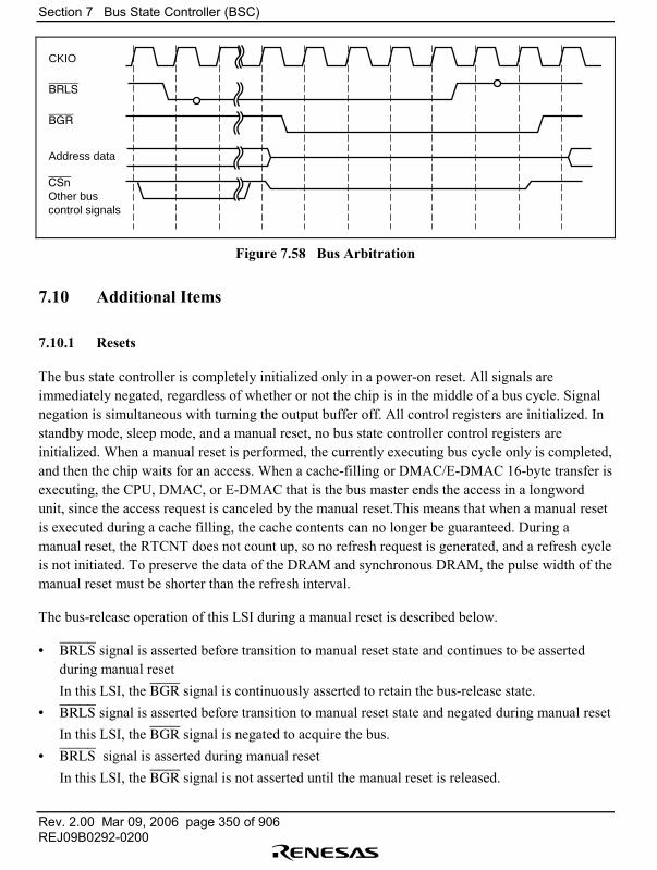
Section 7 Bus State Controller (BSC)
Rev. 2.00 Mar 09, 2006 page 350 of 906REJ09B0292-0200
CKIO
BRLS
BGR
Address data
CSn
Other buscontrol signals
Figure 7.58 Bus Arbitration
7.10 Additional Items
7.10.1 Resets
The bus state controller is completely initialized only in a power-on reset. All signals areimmediately negated, regardless of whether or not the chip is in the middle of a bus cycle. Signalnegation is simultaneous with turning the output buffer off. All control registers are initialized. Instandby mode, sleep mode, and a manual reset, no bus state controller control registers areinitialized. When a manual reset is performed, the currently executing bus cycle only is completed,and then the chip waits for an access. When a cache-filling or DMAC/E-DMAC 16-byte transfer isexecuting, the CPU, DMAC, or E-DMAC that is the bus master ends the access in a longwordunit, since the access request is canceled by the manual reset.This means that when a manual resetis executed during a cache filling, the cache contents can no longer be guaranteed. During amanual reset, the RTCNT does not count up, so no refresh request is generated, and a refresh cycleis not initiated. To preserve the data of the DRAM and synchronous DRAM, the pulse width of themanual reset must be shorter than the refresh interval.
The bus-release operation of this LSI during a manual reset is described below.
• BRLS signal is asserted before transition to manual reset state and continues to be assertedduring manual resetIn this LSI, the BGR signal is continuously asserted to retain the bus-release state.
• BRLS signal is asserted before transition to manual reset state and negated during manual resetIn this LSI, the BGR signal is negated to acquire the bus.
• BRLS signal is asserted during manual resetIn this LSI, the BGR signal is not asserted until the manual reset is released.
Section 7 Bus State Controller (BSC)
Rev. 2.00 Mar 09, 2006 page 351 of 906REJ09B0292-0200
7.10.2 Access as Viewed from CPU, DMAC or E-DMAC
The chip is internally divided into three buses: cache, internal, and peripheral. The CPU and cachememory are connected to the cache bus, the DMAC, E-DMAC and bus state controller areconnected to the internal bus, and the low-speed peripheral devices and mode registers areconnected to the peripheral bus. On-chip memory other than cache memory and the user breakcontroller are connected to both the cache bus and the internal bus. The internal bus can beaccessed from the cache bus, but not the other way around. The peripheral bus can be accessedfrom the internal bus, but not the other way around. This results in the following.
The DMAC can access on-chip memory other than cache memory, but cannot access cachememory. When the DMAC causes a write to external memory, the external memory contents andthe cache contents may be different. When external memory contents are rewritten by a DMAtransfer, the cache memory must be purged by software if there is a possibility that the data forthat address is present in the cache.
When the CPU starts a read access, if the access is to a cache area, a cache search is firstperformed. This takes one cycle. If there is data in the cache, it fetches it and completes the access.If there is no data in the cache, a cache filling is performed via the internal bus, so fourconsecutive longword reads occur. For misses that occur when byte or word operands are accessedor branches occur to odd word boundaries (4n + 2 addresses), the filling is always performed bylongword accesses on the chip-external interface. In the cache-through area, the access is to theactual access address. When the access is an instruction fetch, the access size is always longword.
For cache-through areas and on-chip peripheral module read cycles, after an extra cycle is addedto determine the cycle, the read cycle is started through the internal bus. Read data is sent to theCPU through the cache bus.
When write cycles access the cache area, the cache is searched. When the data of the relevantaddress is found, it is written here. The actual write occurs in parallel to this via the internal bus inwrite-through mode. In write-back mode, the actual write is not performed until a replaceoperation occurs for the relevant address. When the right to use the internal bus is held, the CPU isnotified that the write is completed without waiting for the end of the actual off-chip write. Whenthe right to use the internal bus is not held, as when it is being used by the DMAC or the like, thereis a wait until the bus is acquired before the CPU is notified of completion.
Accesses to cache-through areas and on-chip peripheral modules work the same as in the cachearea, except for the cache search and write.
Because the bus state controller has one level of write buffer, the internal bus can be used foranother access even when the chip-external bus cycle has not ended. After a write has beenperformed to low-speed memory off the chip, performing a read or write with an on-chip
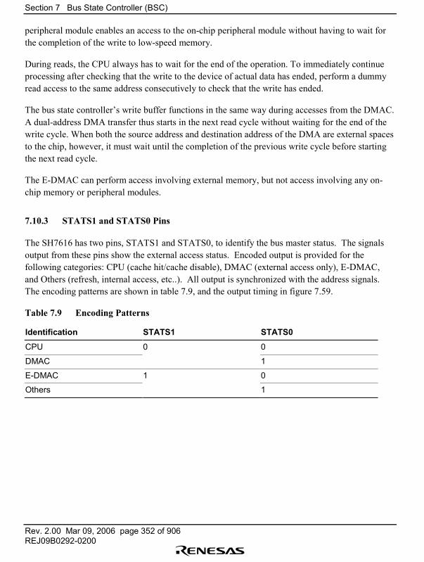
Section 7 Bus State Controller (BSC)
Rev. 2.00 Mar 09, 2006 page 352 of 906REJ09B0292-0200
peripheral module enables an access to the on-chip peripheral module without having to wait forthe completion of the write to low-speed memory.
During reads, the CPU always has to wait for the end of the operation. To immediately continueprocessing after checking that the write to the device of actual data has ended, perform a dummyread access to the same address consecutively to check that the write has ended.
The bus state controller�s write buffer functions in the same way during accesses from the DMAC.A dual-address DMA transfer thus starts in the next read cycle without waiting for the end of thewrite cycle. When both the source address and destination address of the DMA are external spacesto the chip, however, it must wait until the completion of the previous write cycle before startingthe next read cycle.
The E-DMAC can perform access involving external memory, but not access involving any on-chip memory or peripheral modules.
7.10.3 STATS1 and STATS0 Pins
The SH7616 has two pins, STATS1 and STATS0, to identify the bus master status. The signalsoutput from these pins show the external access status. Encoded output is provided for thefollowing categories: CPU (cache hit/cache disable), DMAC (external access only), E-DMAC,and Others (refresh, internal access, etc..). All output is synchronized with the address signals.The encoding patterns are shown in table 7.9, and the output timing in figure 7.59.
Table 7.9 Encoding Patterns
Identification STATS1 STATS0
CPU 0 0
DMAC 1
E-DMAC 1 0
Others 1
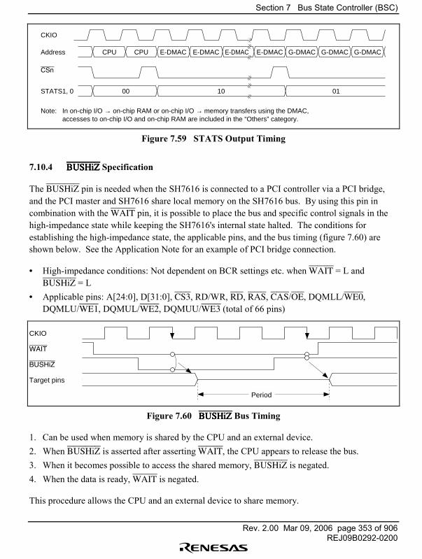
Section 7 Bus State Controller (BSC)
Rev. 2.00 Mar 09, 2006 page 353 of 906REJ09B0292-0200
CKIO
Address CPU CPU E-DMAC E-DMAC E-DMAC G-DMAC G-DMAC G-DMACE-DMAC
STATS1, 0 00 10 01
CSn
Note: In on-chip I/O → on-chip RAM or on-chip I/O → memory transfers using the DMAC, accesses to on-chip I/O and on-chip RAM are included in the “Others” category.
Figure 7.59 STATS Output Timing
7.10.4 BUSHiZBUSHiZBUSHiZBUSHiZ Specification
The BUSHiZ pin is needed when the SH7616 is connected to a PCI controller via a PCI bridge,and the PCI master and SH7616 share local memory on the SH7616 bus. By using this pin incombination with the WAIT pin, it is possible to place the bus and specific control signals in thehigh-impedance state while keeping the SH7616's internal state halted. The conditions forestablishing the high-impedance state, the applicable pins, and the bus timing (figure 7.60) areshown below. See the Application Note for an example of PCI bridge connection.
• High-impedance conditions: Not dependent on BCR settings etc. when WAIT = L andBUSHiZ = L
• Applicable pins: A[24:0], D[31:0], CS3, RD/WR, RD, RAS, CAS/OE, DQMLL/WE0,DQMLU/WE1, DQMUL/WE2, DQMUU/WE3 (total of 66 pins)
CKIO
WAIT
BUSHiZ
Target pins
Period
Figure 7.60 BUSHiZBUSHiZBUSHiZBUSHiZ Bus Timing
1. Can be used when memory is shared by the CPU and an external device.2. When BUSHiZ is asserted after asserting WAIT, the CPU appears to release the bus.3. When it becomes possible to access the shared memory, BUSHiZ is negated.4. When the data is ready, WAIT is negated.
This procedure allows the CPU and an external device to share memory.
Section 7 Bus State Controller (BSC)
Rev. 2.00 Mar 09, 2006 page 354 of 906REJ09B0292-0200
7.11 Usage Notes
7.11.1 Normal Space Access after Synchronous DRAM Write when Using DMAC
Negation of the DQMn/WEn signal in a synchronous DRAM write and CSn assertion in animmediately following normal space access both occur at the same rising edge of CKIO (figure7.61). As there is a risk of an erroneous write to normal space in this case, when synchronousDRAM or a high-speed device is connected to normal space, it is recommended that CSn bedelayed on the system side.
Cases in which a synchronous DRAM write and normal space access occur consecutively areshown in table 7.10.
Table 7.10 access sequence
Write to Synchronous DRAM Normal Space Access
CPU DMA
DMA CPU
DMA DMANote: When an access by the CPU is performed immediately after a write by the CPU, internally
the accesses are not consecutive.
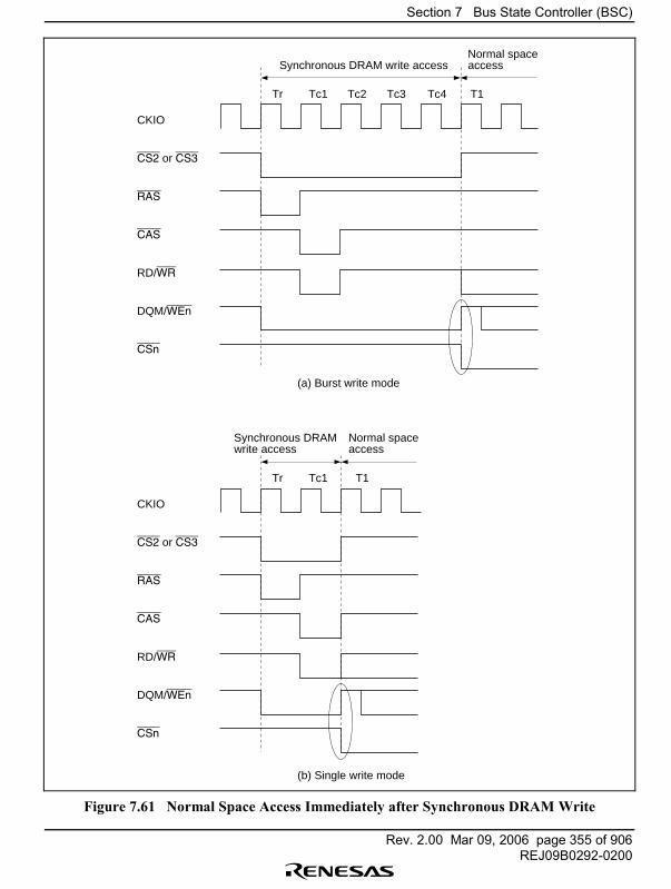
Section 7 Bus State Controller (BSC)
Rev. 2.00 Mar 09, 2006 page 355 of 906REJ09B0292-0200
Tr Tc1 Tc2 Tc3 Tc4 T1
CKIO
CS2 or CS3
RAS
CAS
RD/WR
DQM/WEn
CSn
Tr Tc1 T1
CKIO
CS2 or CS3
RAS
CAS
RD/WR
DQM/WEn
CSn
(a) Burst write mode
(b) Single write mode
Synchronous DRAM write access
Synchronous DRAM write access
Normal space access
Normal space access
Figure 7.61 Normal Space Access Immediately after Synchronous DRAM Write
Section 7 Bus State Controller (BSC)
Rev. 2.00 Mar 09, 2006 page 356 of 906REJ09B0292-0200
7.11.2 When Using Iφφφφ: Eφφφφ Clock Ratio of 1: 1, 8-Bit Bus Width, and External Wait Input
When using an Iφ: Eφ clock ratio of 1: 1 and an 8-bit bus width, at least 1.5 address hold cyclesshould be set.
Set a value other than the initial value in bits AnSHW1, AnSHW0, A4HW1, and A4HW0 for therelevant space.
7.11.3 When connecting external device to synchronous DRAM
When connecting an external device to the synchronous DRAM, not only CSnN and DACKn butalso other instructions for the synchronous DRAM such as CSnN, RASN, CASN and RDWRNmust be recognized for the estimation of an access sequence.
In some cases, it is difficult to specify read and write cycles only with CSnN and DACKn.
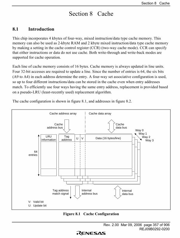
Section 8 Cache
Rev. 2.00 Mar 09, 2006 page 357 of 906REJ09B0292-0200
Section 8 Cache
8.1 Introduction
This chip incorporates 4 kbytes of four-way, mixed instruction/data type cache memory. Thismemory can also be used as 2-kbyte RAM and 2 kbyte mixed instruction/data type cache memoryby making a setting in the cache control register (CCR) (two-way cache mode). CCR can specifythat either instructions or data do not use cache. Both write-through and write-back modes aresupported for cache operation.
Each line of cache memory consists of 16 bytes. Cache memory is always updated in line units.Four 32-bit accesses are required to update a line. Since the number of entries is 64, the six bits(A9 to A4) in each address determine the entry. A four-way set associative configuration is used,so up to four different instructions/data can be stored in the cache even when entry addressesmatch. To efficiently use four ways having the same entry address, replacement is provided basedon a pseudo-LRU (least-recently used) replacement algorithm.
The cache configuration is shown in figure 8.1, and addresses in figure 8.2.
64entries
Internaldata bus
Internaladdress bus
Tag addressmatch signal
Cachedata bus
Way 0Way 1
Way 2Way 3
Cacheaddress bus
Cache data arrayCache address array
Tagaddress
LRUinformation Data (16 bytes/line)U V
V: Valid bitU: Update bit
Figure 8.1 Cache Configuration

Section 8 Cache
Rev. 2.00 Mar 09, 2006 page 358 of 906REJ09B0292-0200
31 28 9 3
3 19 6 4
0
Byte addressin line
Entry addressTag addressAccess spacespecification address
Address
Bit
Number of bits
Figure 8.2 Address Configuration
8.1.1 Register Configuration
Table 8.1 shows the cache register configuration.
Table 8.1 Register Configuration
Name Abbrev. R/W Initial Value Address
Cache control register CCR R/W H'00 H'FFFFFE92
8.2 Register Description
8.2.1 Cache Control Register (CCR)
The cache control register (CCR) is used for cache control. CCR must be set and the cache mustbe initialized before use. CCR is initialized to H'00 by a power-on reset or manual reset.
Bit: 7 6 5 4 3 2 1 0
W1 W0 WB CP TW OD ID CE
Initial value: 0 0 0 0 0 0 0 0
R/W: R/W R/W R/W R/W R/W R/W R/W R/W
Bits 7 and 6�Way Specification Bit (W1, W0): W1 and W0 specify the way when an addressarray is directly accessed by address specification.
Bit 7: W1 Bit 6: W0 Description
0 0 Way 0 (Initial value)
1 Way 1
1 0 Way 2
1 Way 3
Section 8 Cache
Rev. 2.00 Mar 09, 2006 page 359 of 906REJ09B0292-0200
Bit 5�Write-Back Bit (WB): Specifies the cache operation method when the cache area isaccessed.
Bit 5: WB Description
0 Write-through (Initial value)
1 Write-back
Bit 4�Cache Purge Bit (CP): When 1 is written to the CP bit, all cache entries and the valid bits,and LRU information of all ways are initialized to 0. After initialization is completed, the CP bitreverts to 0. The CP bit always reads 0.
Bit 4: CP Description
0 Normal operation (Initial value)
1 Cache purgeNote: Always read 0.
Bit 3�Two-Way Mode (TW): TW is the two-way mode bit. The cache operates as a four-way setassociative cache when TW is 0 and as a two-way set associative cache and 2-kbyte RAM whenTW is 1. In the two-way mode, ways 2 and 3 are cache and ways 0 and 1 are RAM. Ways 0 and 1are read or written by direct access of the data array according to address space specification.
Bit 3: TW Description
0 Four-way mode (Initial value)
1 Two-way mode
Bit 2�Data Replacement Disable Bit (OD): OD is the bit for disabling data replacement. Whenthis bit is 1, data fetched from external memory is not written to the cache even if there is a cachemiss. Cache data is, however, read or updated during cache hits. OD is valid only when CE is 1.
Bit 2: OD Description
0 Normal operation (Initial value)
1 Data not replaced even when cache miss occurs in data access
Section 8 Cache
Rev. 2.00 Mar 09, 2006 page 360 of 906REJ09B0292-0200
Bit 1�Instruction Replacement Disable Bit (ID): ID is the bit for disabling instructionreplacement. When this bit is 1, an instruction fetched from external memory is not written to thecache even if there is a cache miss. Cache data is, however, read or updated during cache hits. IDis valid only when CE is 1.
Bit 1: ID Description
0 Normal operation (Initial value)
1 Data not replaced even when cache miss occurs in instruction fetch
Bit 0�Cache Enable Bit (CE): CE is the cache enable bit. Cache can be used when CE is set to 1.
Bit 0: CE Description
0 Cache disabled (Initial value)
1 Cache enabled
8.3 Address Space and the Cache
The address space is divided into six partitions. The cache access operation is specified byaddresses. Table 8.2 lists the partitions and their cache operations. For more information onaddress spaces, see section 7, Bus State Controller. Note that the spaces of the cache area andcache-through area are the same.
Table 8.2 Address Space and Cache Operation
AddressesA31�A29 Partition Cache Operation
000 Cache area Cache is used when the CE bit in CCR is 1
001 Cache-through area Cache is not used
010 Associative purge area Cache line of the specified address is purged(disabled)
011 Address array read/write area Cache address array is accessed directly
110 Data array read/write area Cache data array is accessed directly
111 I/O area Cache is not used
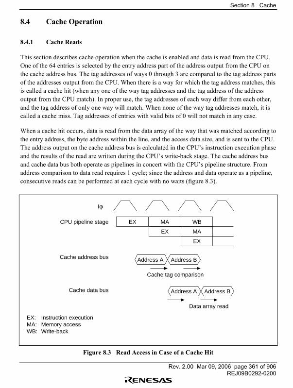
Section 8 Cache
Rev. 2.00 Mar 09, 2006 page 361 of 906REJ09B0292-0200
8.4 Cache Operation
8.4.1 Cache Reads
This section describes cache operation when the cache is enabled and data is read from the CPU.One of the 64 entries is selected by the entry address part of the address output from the CPU onthe cache address bus. The tag addresses of ways 0 through 3 are compared to the tag address partsof the addresses output from the CPU. When there is a way for which the tag address matches, thisis called a cache hit (when any one of the way tag addresses and the tag address of the addressoutput from the CPU match). In proper use, the tag addresses of each way differ from each other,and the tag address of only one way will match. When none of the way tag addresses match, it iscalled a cache miss. Tag addresses of entries with valid bits of 0 will not match in any case.
When a cache hit occurs, data is read from the data array of the way that was matched according tothe entry address, the byte address within the line, and the access data size, and is sent to the CPU.The address output on the cache address bus is calculated in the CPU�s instruction execution phaseand the results of the read are written during the CPU�s write-back stage. The cache address busand cache data bus both operate as pipelines in concert with the CPU�s pipeline structure. Fromaddress comparison to data read requires 1 cycle; since the address and data operate as a pipeline,consecutive reads can be performed at each cycle with no waits (figure 8.3).
EXCPU pipeline stage
Iφ
Cache address bus
Cache data bus
MA WB
EX
Address A
Cache tag comparison
Address B
MA
EX
Address A
Data array read
Address B
EX: Instruction executionMA: Memory accessWB: Write-back
Figure 8.3 Read Access in Case of a Cache Hit
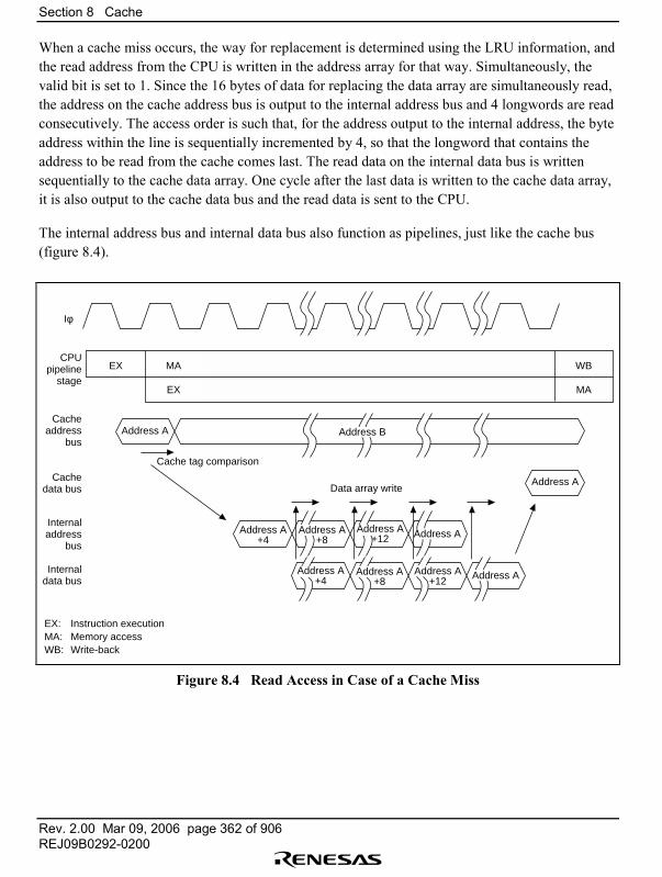
Section 8 Cache
Rev. 2.00 Mar 09, 2006 page 362 of 906REJ09B0292-0200
When a cache miss occurs, the way for replacement is determined using the LRU information, andthe read address from the CPU is written in the address array for that way. Simultaneously, thevalid bit is set to 1. Since the 16 bytes of data for replacing the data array are simultaneously read,the address on the cache address bus is output to the internal address bus and 4 longwords are readconsecutively. The access order is such that, for the address output to the internal address, the byteaddress within the line is sequentially incremented by 4, so that the longword that contains theaddress to be read from the cache comes last. The read data on the internal data bus is writtensequentially to the cache data array. One cycle after the last data is written to the cache data array,it is also output to the cache data bus and the read data is sent to the CPU.
The internal address bus and internal data bus also function as pipelines, just like the cache bus(figure 8.4).
Address A
MA
EX
EX WB
MA
Data array write
Address B
Address A+12 Address AAddress A
+8Address A
+4
Address A+4
Address A+8
Address A+12 Address A
Cache tag comparison
CPUpipeline
stage
Iφ
Cacheaddress
bus
Cachedata bus
Internaladdress
bus
Internaldata bus
EX: Instruction executionMA: Memory accessWB: Write-back
Address A
Figure 8.4 Read Access in Case of a Cache Miss
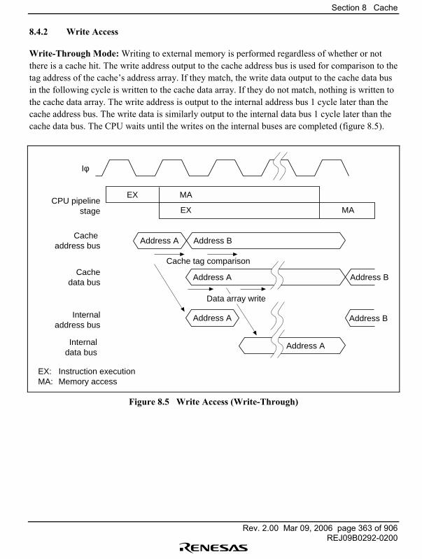
Section 8 Cache
Rev. 2.00 Mar 09, 2006 page 363 of 906REJ09B0292-0200
8.4.2 Write Access
Write-Through Mode: Writing to external memory is performed regardless of whether or notthere is a cache hit. The write address output to the cache address bus is used for comparison to thetag address of the cache�s address array. If they match, the write data output to the cache data busin the following cycle is written to the cache data array. If they do not match, nothing is written tothe cache data array. The write address is output to the internal address bus 1 cycle later than thecache address bus. The write data is similarly output to the internal data bus 1 cycle later than thecache data bus. The CPU waits until the writes on the internal buses are completed (figure 8.5).
Address A
CPU pipelinestage
Iφ
Cache address bus
Cachedata bus
MAEX
Internaldata bus
EX MA
Address B
Address A
Address A
Address A Address B
Address BInternaladdress bus
Cache tag comparison
Data array write
EX: Instruction executionMA: Memory access
Figure 8.5 Write Access (Write-Through)

Section 8 Cache
Rev. 2.00 Mar 09, 2006 page 364 of 906REJ09B0292-0200
Write-Back Mode: When a cache hit occurs, the data is written to the data array of the matchingway according to the entry address, byte address in the line, and access data size, and the updatebit of that entry is set to 1. A write is performed only to the data array, not to external memory. Awrite hit is completed in 2 cycles (figure 8.6).
EX MA
EX MA
EX
Address A Address B Address C
Address A Address B
CPU pipelinestage
Iφ
Cacheaddress bus
Cachedata bus
EX: Instruction executionMA: Memory access
Cache tag comparison Cache tag comparison
Data array write
Figure 8.6 Write Access in Case of a Cache Hit (Write-Back)
When a cache miss occurs, the way for replacement is determined using the LRU information, andthe write address from the CPU is written in the address array for that way. Simultaneously, thevalid bit and update bit are set to 1. Since the 16 bytes of data for replacing the data array aresimultaneously read when the data on the cache bus is written to the cache, the address on thecache address bus is output to the internal address bus and 4 longwords are read consecutively.The access order is such that, for the address output to the internal address, the byte address withinthe line is sequentially incremented by 4, so that the longword that contains the address to be readfrom the cache comes last. The read data on the internal data bus is written sequentially to thecache data array.
The internal address bus and internal data bus also function as pipelines, just like the cache bus(figure 8.7).
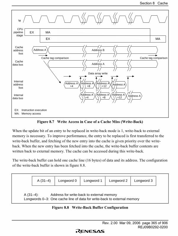
Section 8 Cache
Rev. 2.00 Mar 09, 2006 page 365 of 906REJ09B0292-0200
Address A
MA
EX
EX
MA
Cache tag comparison Cache tag comparison
Data array write
Address AAddress A +12
Address A +8
Address A+4
Address AAddress A +12
Address A +8
Address A+4
Address B
Address A
CPUpipeline
stage
Iφ
Cacheaddress
bus
Cachedata bus
Internaladdress
bus
EX: Instruction executionMA: Memory access
Internaldata bus
Figure 8.7 Write Access in Case of a Cache Miss (Write-Back)
When the update bit of an entry to be replaced in write-back mode is 1, write-back to externalmemory is necessary. To improve performance, the entry to be replaced is first transferred to thewrite-back buffer, and fetching of the new entry into the cache is given priority over the write-back. When the new entry has been fetched into the cache, the write-back buffer contents arewritten back to external memory. The cache can be accessed during this write-back.
The write-back buffer can hold one cache line (16 bytes) of data and its address. The configurationof the write-back buffer is shown in figure 8.8.
A (31–4): Address for write-back to external memoryLongwords 0–3: One cache line of data for write-back to external memory
A (31–4) Longword 0 Longword 1 Longword 2 Longword 3
Figure 8.8 Write-Back Buffer Configuration
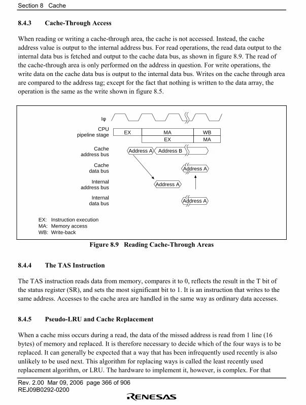
Section 8 Cache
Rev. 2.00 Mar 09, 2006 page 366 of 906REJ09B0292-0200
8.4.3 Cache-Through Access
When reading or writing a cache-through area, the cache is not accessed. Instead, the cacheaddress value is output to the internal address bus. For read operations, the read data output to theinternal data bus is fetched and output to the cache data bus, as shown in figure 8.9. The read ofthe cache-through area is only performed on the address in question. For write operations, thewrite data on the cache data bus is output to the internal data bus. Writes on the cache through areaare compared to the address tag; except for the fact that nothing is written to the data array, theoperation is the same as the write shown in figure 8.5.
EXCPU
pipeline stage
Iφ
Cacheaddress bus
Cachedata bus
Internaladdress bus
Internaldata bus
MA WBEX MA
Address A
Address A
Address B
Address A
Address A
EX: Instruction executionMA: Memory accessWB: Write-back
Figure 8.9 Reading Cache-Through Areas
8.4.4 The TAS Instruction
The TAS instruction reads data from memory, compares it to 0, reflects the result in the T bit ofthe status register (SR), and sets the most significant bit to 1. It is an instruction that writes to thesame address. Accesses to the cache area are handled in the same way as ordinary data accesses.
8.4.5 Pseudo-LRU and Cache Replacement
When a cache miss occurs during a read, the data of the missed address is read from 1 line (16bytes) of memory and replaced. It is therefore necessary to decide which of the four ways is to bereplaced. It can generally be expected that a way that has been infrequently used recently is alsounlikely to be used next. This algorithm for replacing ways is called the least recently usedreplacement algorithm, or LRU. The hardware to implement it, however, is complex. For that
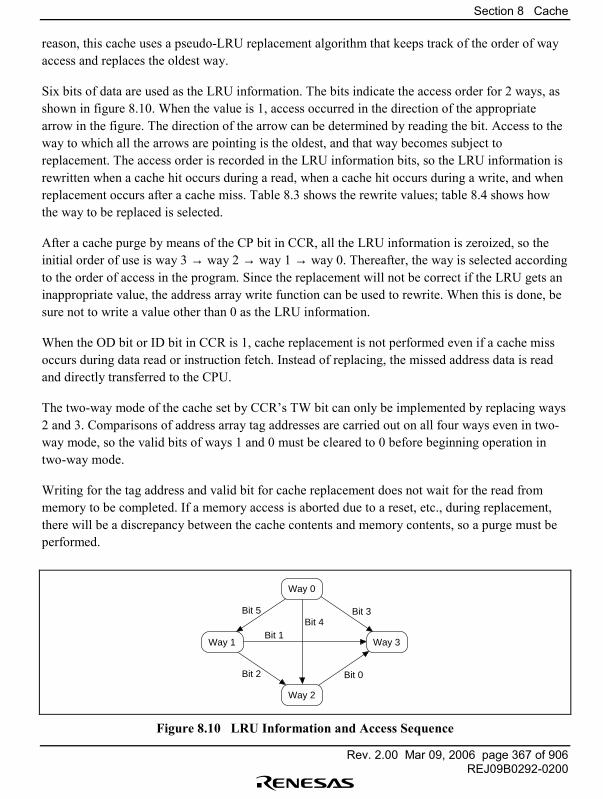
Section 8 Cache
Rev. 2.00 Mar 09, 2006 page 367 of 906REJ09B0292-0200
reason, this cache uses a pseudo-LRU replacement algorithm that keeps track of the order of wayaccess and replaces the oldest way.
Six bits of data are used as the LRU information. The bits indicate the access order for 2 ways, asshown in figure 8.10. When the value is 1, access occurred in the direction of the appropriatearrow in the figure. The direction of the arrow can be determined by reading the bit. Access to theway to which all the arrows are pointing is the oldest, and that way becomes subject toreplacement. The access order is recorded in the LRU information bits, so the LRU information isrewritten when a cache hit occurs during a read, when a cache hit occurs during a write, and whenreplacement occurs after a cache miss. Table 8.3 shows the rewrite values; table 8.4 shows howthe way to be replaced is selected.
After a cache purge by means of the CP bit in CCR, all the LRU information is zeroized, so theinitial order of use is way 3 → way 2 → way 1 → way 0. Thereafter, the way is selected accordingto the order of access in the program. Since the replacement will not be correct if the LRU gets aninappropriate value, the address array write function can be used to rewrite. When this is done, besure not to write a value other than 0 as the LRU information.
When the OD bit or ID bit in CCR is 1, cache replacement is not performed even if a cache missoccurs during data read or instruction fetch. Instead of replacing, the missed address data is readand directly transferred to the CPU.
The two-way mode of the cache set by CCR�s TW bit can only be implemented by replacing ways2 and 3. Comparisons of address array tag addresses are carried out on all four ways even in two-way mode, so the valid bits of ways 1 and 0 must be cleared to 0 before beginning operation intwo-way mode.
Writing for the tag address and valid bit for cache replacement does not wait for the read frommemory to be completed. If a memory access is aborted due to a reset, etc., during replacement,there will be a discrepancy between the cache contents and memory contents, so a purge must beperformed.
Way 0
Way 2
Way 1 Way 3
Bit 5
Bit 2
Bit 3Bit 4
Bit 1
Bit 0
Figure 8.10 LRU Information and Access Sequence
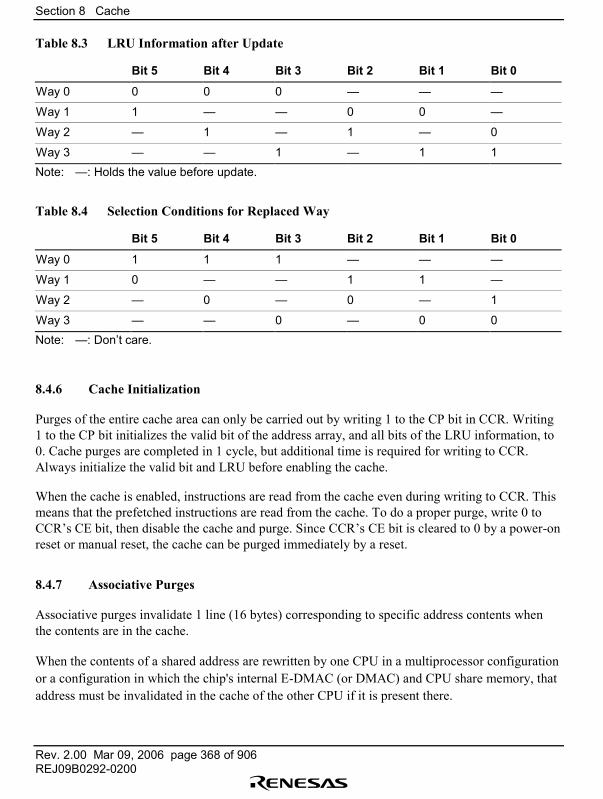
Section 8 Cache
Rev. 2.00 Mar 09, 2006 page 368 of 906REJ09B0292-0200
Table 8.3 LRU Information after Update
Bit 5 Bit 4 Bit 3 Bit 2 Bit 1 Bit 0
Way 0 0 0 0 � � �
Way 1 1 � � 0 0 �
Way 2 � 1 � 1 � 0
Way 3 � � 1 � 1 1Note: �: Holds the value before update.
Table 8.4 Selection Conditions for Replaced Way
Bit 5 Bit 4 Bit 3 Bit 2 Bit 1 Bit 0
Way 0 1 1 1 � � �
Way 1 0 � � 1 1 �
Way 2 � 0 � 0 � 1
Way 3 � � 0 � 0 0Note: �: Don�t care.
8.4.6 Cache Initialization
Purges of the entire cache area can only be carried out by writing 1 to the CP bit in CCR. Writing1 to the CP bit initializes the valid bit of the address array, and all bits of the LRU information, to0. Cache purges are completed in 1 cycle, but additional time is required for writing to CCR.Always initialize the valid bit and LRU before enabling the cache.
When the cache is enabled, instructions are read from the cache even during writing to CCR. Thismeans that the prefetched instructions are read from the cache. To do a proper purge, write 0 toCCR�s CE bit, then disable the cache and purge. Since CCR�s CE bit is cleared to 0 by a power-onreset or manual reset, the cache can be purged immediately by a reset.
8.4.7 Associative Purges
Associative purges invalidate 1 line (16 bytes) corresponding to specific address contents whenthe contents are in the cache.
When the contents of a shared address are rewritten by one CPU in a multiprocessor configurationor a configuration in which the chip's internal E-DMAC (or DMAC) and CPU share memory, thataddress must be invalidated in the cache of the other CPU if it is present there.
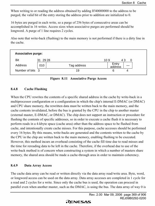
Section 8 Cache
Rev. 2.00 Mar 09, 2006 page 369 of 906REJ09B0292-0200
When writing to or reading the address obtained by adding H'40000000 to the address to bepurged, the valid bit of the entry storing the address prior to addition are initialized to 0.
16 bytes are purged in each write, so a purge of 256 bytes of consecutive areas can beaccomplished in 16 writes. Access sizes when associative purges are performed should belongword. A purge of 1 line requires 2 cycles.
Also note that write-back (flushing) to the main memory is not performed if there is a dirty line inthe cache.
Tag address010 Entryaddress —
31 10 9 4 3 0
19 63 4
29 28
Associative purge:
Address
Bit
Number of bits
Figure 8.11 Associative Purge Access
8.4.8 Cache Flushing
When the CPU rewrites the contents of a specific shared address in the cache by write-back in amultiprocessor configuration or a configuration in which the chip's internal E-DMAC (or DMAC)and CPU share memory, the rewritten data must be written back to the main memory, and thecache contents invalidated, before the bus is granted by the CPU in the chip to another master(external master, E-DMAC, or DMAC). The chip does not support an instruction or procedure forflushing the contents of specific addresses, so in order to execute a cache flush it is necessary toperform reads in a 4-kbyte space (cache area) other than the address space to be flushed fromcache, and intentionally create cache misses. For this purpose, cache accesses should be performedevery 16 bytes. By this means, write-backs are generated and the contents written to the cache bythe CPU in the chip are written back to the main memory, enabling flushing to be executed.However, this method incurs an overhead consisting of the cache fill time due to read misses andthe time for rereading data to be left in the cache. Therefore, if the overhead due to use of thewrite-back method is of concern when constructing a system in which a number of masters sharememory, the shared area should be made a cache-through area in order to maintain coherency.
8.4.9 Data Array Access
The cache data array can be read or written directly via the data array read/write area. Byte, word,or longword access can be used on the data array. Data array accesses are completed in 1 cycle fora read and 2 cycles for a write. Since only the cache bus is used, the operation can proceed inparallel even when another master, such as the DMAC, is using the bus. The data array of way 0 is
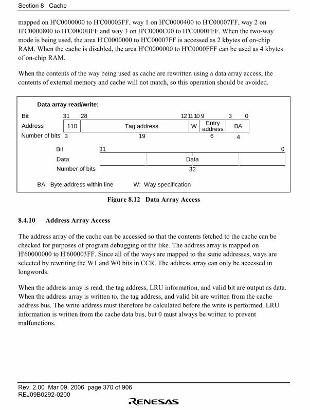
Section 8 Cache
Rev. 2.00 Mar 09, 2006 page 370 of 906REJ09B0292-0200
mapped on H'C0000000 to H'C00003FF, way 1 on H'C0000400 to H'C00007FF, way 2 onH'C0000800 to H'C0000BFF and way 3 on H'C0000C00 to H'C0000FFF. When the two-waymode is being used, the area H'C0000000 to H'C00007FF is accessed as 2 kbytes of on-chipRAM. When the cache is disabled, the area H'C0000000 to H'C0000FFF can be used as 4 kbytesof on-chip RAM.
When the contents of the way being used as cache are rewritten using a data array access, thecontents of external memory and cache will not match, so this operation should be avoided.
Tag address110 Entryaddress BAW
31 28 9101112 3 0
19
Data
31 0
32
63 4
Data
Data array read/write:
BA: Byte address within line W: Way specification
Address
Bit
Number of bits
Bit
Number of bits
Figure 8.12 Data Array Access
8.4.10 Address Array Access
The address array of the cache can be accessed so that the contents fetched to the cache can bechecked for purposes of program debugging or the like. The address array is mapped onH'60000000 to H'600003FF. Since all of the ways are mapped to the same addresses, ways areselected by rewriting the W1 and W0 bits in CCR. The address array can only be accessed inlongwords.
When the address array is read, the tag address, LRU information, and valid bit are output as data.When the address array is written to, the tag address, and valid bit are written from the cacheaddress bus. The write address must therefore be calculated before the write is performed. LRUinformation is written from the cache data bus, but 0 must always be written to preventmalfunctions.
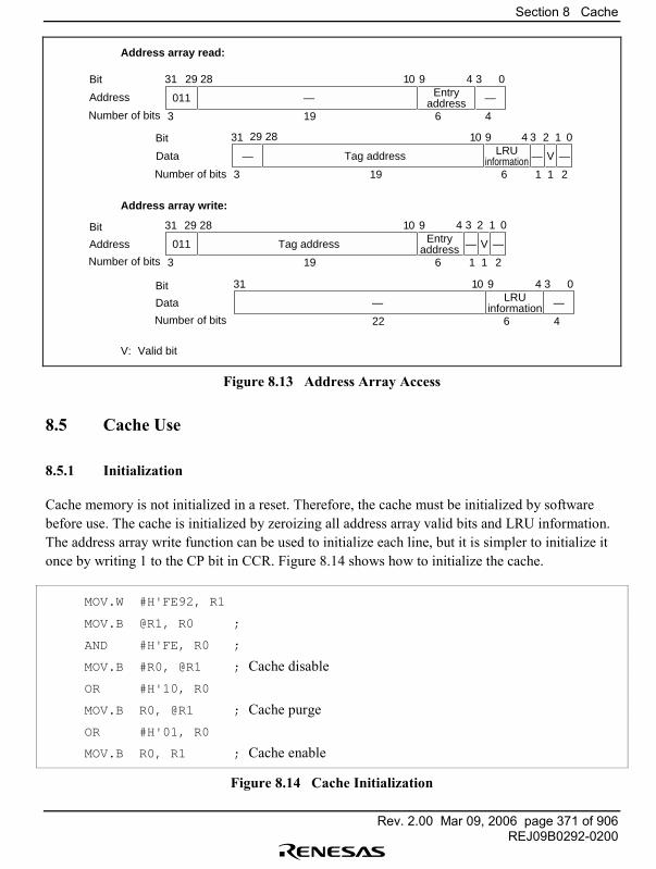
Section 8 Cache
Rev. 2.00 Mar 09, 2006 page 371 of 906REJ09B0292-0200
—011 Entryaddress —
31 2829 910 34 0
19 63 4
Tag address—Data LRUinformation —— V
31 910 34 2 0
19 63 1 1 2
— LRUinformation —
31 910 34 0
22 6 4
Data
Tag address011 Entryaddress —— V
31 2829 910
19 63 1 1 2
Address array read:
Address array write:
V: Valid bit
1
34 2 01
2829
Address
Bit
Number of bits
Bit
Number of bits
Address
Bit
Number of bits
Bit
Number of bits
Figure 8.13 Address Array Access
8.5 Cache Use
8.5.1 Initialization
Cache memory is not initialized in a reset. Therefore, the cache must be initialized by softwarebefore use. The cache is initialized by zeroizing all address array valid bits and LRU information.The address array write function can be used to initialize each line, but it is simpler to initialize itonce by writing 1 to the CP bit in CCR. Figure 8.14 shows how to initialize the cache.
MOV.W #H'FE92, R1
MOV.B @R1, R0 ;
AND #H'FE, R0 ;
MOV.B #R0, @R1 ; Cache disable OR #H'10, R0
MOV.B R0, @R1 ; Cache purge OR #H'01, R0
MOV.B R0, R1 ; Cache enable
Figure 8.14 Cache Initialization
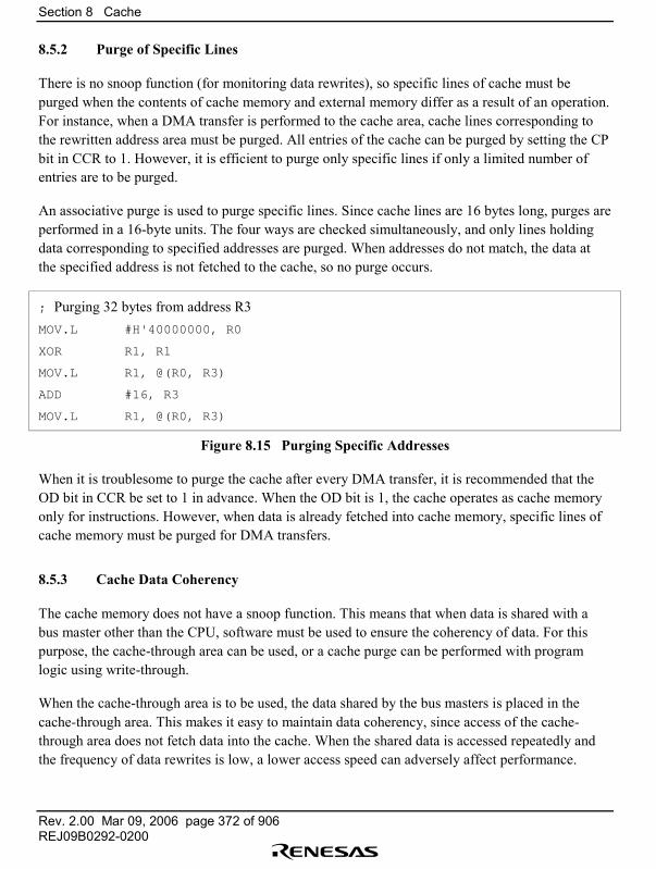
Section 8 Cache
Rev. 2.00 Mar 09, 2006 page 372 of 906REJ09B0292-0200
8.5.2 Purge of Specific Lines
There is no snoop function (for monitoring data rewrites), so specific lines of cache must bepurged when the contents of cache memory and external memory differ as a result of an operation.For instance, when a DMA transfer is performed to the cache area, cache lines corresponding tothe rewritten address area must be purged. All entries of the cache can be purged by setting the CPbit in CCR to 1. However, it is efficient to purge only specific lines if only a limited number ofentries are to be purged.
An associative purge is used to purge specific lines. Since cache lines are 16 bytes long, purges areperformed in a 16-byte units. The four ways are checked simultaneously, and only lines holdingdata corresponding to specified addresses are purged. When addresses do not match, the data atthe specified address is not fetched to the cache, so no purge occurs.
; Purging 32 bytes from address R3MOV.L #H'40000000, R0
XOR R1, R1
MOV.L R1, @(R0, R3)
ADD #16, R3
MOV.L R1, @(R0, R3)
Figure 8.15 Purging Specific Addresses
When it is troublesome to purge the cache after every DMA transfer, it is recommended that theOD bit in CCR be set to 1 in advance. When the OD bit is 1, the cache operates as cache memoryonly for instructions. However, when data is already fetched into cache memory, specific lines ofcache memory must be purged for DMA transfers.
8.5.3 Cache Data Coherency
The cache memory does not have a snoop function. This means that when data is shared with abus master other than the CPU, software must be used to ensure the coherency of data. For thispurpose, the cache-through area can be used, or a cache purge can be performed with programlogic using write-through.
When the cache-through area is to be used, the data shared by the bus masters is placed in thecache-through area. This makes it easy to maintain data coherency, since access of the cache-through area does not fetch data into the cache. When the shared data is accessed repeatedly andthe frequency of data rewrites is low, a lower access speed can adversely affect performance.

Section 8 Cache
Rev. 2.00 Mar 09, 2006 page 373 of 906REJ09B0292-0200
To purge the cache using program logic, the data updates are detected by the program flow and thecache is then purged. For example, if the program inputs data from a disk, whenever reading of aunit (such as a sector) is completed, the buffer address used for reading or the entire cache ispurged, thereby maintaining coherency. When data is to be exchanged between two processors,only flags that provide mutual notification of completion of data preparation or completion of afetch are placed in the cache-through area. The data actually to be transferred is placed in thecache area and the cache is purged before the first data read to maintain the coherency of the data.When semaphores are used as the means of communication, data coherency can be maintainedeven when the cache is not purged by utilizing the TAS instruction. Direct external access mustalways be used for a TAS instruction read.
When the update unit is small, specific addresses can be purged, so only the relevant addresses arepurged. When the update unit is larger, it is faster to purge the entire cache rather than purging allthe addresses in order, and then read the data that previously existed in the cache again fromexternal memory.
When write-back is used, coherency can be maintained by executing write-backs (flushing) tomemory by means of intentional cache miss reads, but since executing flushing incurs anoverhead, use of write-through or accessing the cache-through area is recommended in a system inwhich a number of masters share memory.
8.5.4 Two-Way Cache Mode
The 4-kbyte cache can be used as 2-kbyte RAM and 2-kbyte mixed instruction/data cache memoryby setting the TW bit in CCR to 1. Ways 2 and 3 become cache, and ways 0 and 1 become RAM.
Initialization is performed by writing 1 to the CP bit in CCR, in the same way as with 4 ways. Thevalid bit, and LRU bits are cleared to 0.
When LRU information is initialized to zero, the initial order of use is way 3 → way 2. Thereafter,way 3 or way 2 is selected for replacement in accordance with the LRU information. Theconditions for updating the LRU information are the same as for four-way mode, except that thenumber of ways is two.
When designated as 2-kbyte RAM, ways 0 and 1 are accessed by data array access. Figure 8.16shows the address mapping.
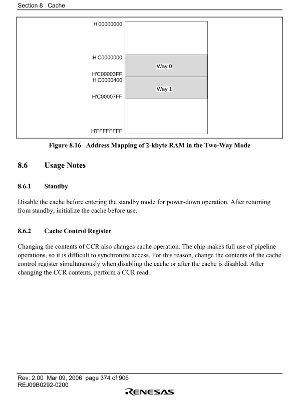
Section 8 Cache
Rev. 2.00 Mar 09, 2006 page 374 of 906REJ09B0292-0200
H'C0000000
H'C00003FFH'C0000400
H'C00007FF
Way 0
Way 1
H'00000000
H'FFFFFFFF
Figure 8.16 Address Mapping of 2-kbyte RAM in the Two-Way Mode
8.6 Usage Notes
8.6.1 Standby
Disable the cache before entering the standby mode for power-down operation. After returningfrom standby, initialize the cache before use.
8.6.2 Cache Control Register
Changing the contents of CCR also changes cache operation. The chip makes full use of pipelineoperations, so it is difficult to synchronize access. For this reason, change the contents of the cachecontrol register simultaneously when disabling the cache or after the cache is disabled. Afterchanging the CCR contents, perform a CCR read.
Section 9 Ethernet Controller (EtherC)
Rev. 2.00 Mar 09, 2006 page 375 of 906REJ09B0292-0200
Section 9 Ethernet Controller (EtherC)
9.1 Overview
The SH7616 has an on-chip Ethernet controller (EtherC) conforming to the IEEE802.3 MAC(Media Access Control) layer standard. Connecting a physical-layer LSI (PHY-LSI) complyingwith this standard enables the Ethernet controller (EtherC) to perform transmission and receptionof Ethernet/IEEE802.3 frames. The Ethernet controller is connected to dedicated transmit andreceive Ethernet DMACs (E-DMACs) in the SH7616, and carries out high-speed data transfer toand from memory.
9.1.1 Features
The EtherC has the following features:
• Transmission and reception of Ethernet/IEEE802.3 frames• Supports 10/100 Mbps transfer• Supports full-duplex and half-duplex modes• Conforms to IEEE802.3u standard MII (Media Independent Interface)• Magic Packet detection and Wake On LAN (WOL) signal output• CAM (Content Addressable Memory) match signal input function
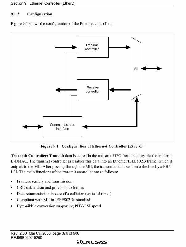
Section 9 Ethernet Controller (EtherC)
Rev. 2.00 Mar 09, 2006 page 376 of 906REJ09B0292-0200
9.1.2 Configuration
Figure 9.1 shows the configuration of the Ethernet controller.
Transmitcontroller
Receivecontroller
Command statusinterface
MII
Figure 9.1 Configuration of Ethernet Controller (EtherC)
Transmit Controller: Transmit data is stored in the transmit FIFO from memory via the transmitE-DMAC. The transmit controller assembles this data into an Ethernet/IEEE802.3 frame, which itoutputs to the MII. After passing through the MII, the transmit data is sent onto the line by a PHY-LSI. The main functions of the transmit controller are as follows:
• Frame assembly and transmission• CRC calculation and provision to frames• Data retransmission in case of a collision (up to 15 times)• Compliant with MII in IEEE802.3u standard• Byte-nibble conversion supporting PHY-LSI speed
Section 9 Ethernet Controller (EtherC)
Rev. 2.00 Mar 09, 2006 page 377 of 906REJ09B0292-0200
Receive Controller: After a frame is received via the MII, the receive controller carries outaddress information, frame length, CRC, and other checks, and the receive data is transferred tomemory by the receive E-DMAC. The main functions of the receive controller are as follows:
• Checking received frame format• Checking receive frame CRC and frame length• Transfer of own-address, multicast, or broadcast receive frames to memory• Compliant with MII in IEEE802.3u standard• Nibble-byte conversion supporting PHY-LSI speed• Magic Packet monitoring• CAM (Content Addressable Memory) match signal input function
Command/Status Interface: This interface provides various command/status registers to controlthe EtherC, and performs access to PHY-LSI internal registers via the MII.
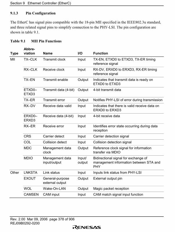
Section 9 Ethernet Controller (EtherC)
Rev. 2.00 Mar 09, 2006 page 378 of 906REJ09B0292-0200
9.1.3 Pin Configuration
The EtherC has signal pins compatible with the 18-pin MII specified in the IEEE802.3u standard,and three related signal pins to simplify connection to the PHY-LSI. The pin configuration areshown in table 9.1.
Table 9.1 MII Pin Functions
TypeAbbre-viation Name I/O Function
MII TX�CLK Transmit clock Input TX-EN, ETXD0 to ETXD3, TX-ER timingreference signal
RX�CLK Receive clock Input RX-DV, ERXD0 to ERXD3, RX-ER timingreference signal
TX�EN Transmit enable Output Indicates that transmit data is ready onETXD0 to ETXD3
ETXD0�ETXD3
Transmit data (4-bit) Output 4-bit transmit data
TX�ER Transmit error Output Notifies PHY-LSI of error during transmission
RX�DV Receive data valid Input Indicates that there is valid receive data onERXD0 to ERXD3
ERXD0�ERXD3
Receive data (4-bit) Input 4-bit receive data
RX�ER Receive error Input Identifies error state occurring during datareception
CRS Carrier detect Input Carrier detection signal
COL Collision detect Input Collision detection signal
MDC Management dataclock
Output Reference clock signal for informationtransfer via MDIO
MDIO Management datainput/output
Input/output
Bidirectional signal for exchange ofmanagement information between STA andPHY
Other LNKSTA Link status Input Inputs link status from PHY-LSI
EXOUT General-purposeexternal output
Output External output pin
WOL Wake-On-LAN Output Magic packet reception
CAMSEN CAM input Input CAM match signal input function
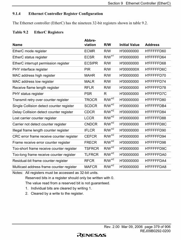
Section 9 Ethernet Controller (EtherC)
Rev. 2.00 Mar 09, 2006 page 379 of 906REJ09B0292-0200
9.1.4 Ethernet Controller Register Configuration
The Ethernet controller (EtherC) has the nineteen 32-bit registers shown in table 9.2.
Table 9.2 EtherC Registers
NameAbbre-viation R/W Initial Value Address
EtherC mode register ECMR R/W H'00000000 H'FFFFFD60
EtherC status register ECSR R/W*1 H'00000000 H'FFFFFD64
EtherC interrupt permission register ECSIPR R/W H'00000000 H'FFFFFD68
PHY interface register PIR R/W H'0000000X H'FFFFFD6C
MAC address high register MAHR R/W H'00000000 H'FFFFFD70
MAC address low register MALR R/W H'00000000 H'FFFFFD74
Receive flame length register RFLR R/W H'00000000 H'FFFFFD78
PHY status register PSR R H'00000000 H'FFFFFD7C
Transmit retry over counter register TROCR R/W*2 H'00000000 H'FFFFFD80
Single Collision detect counter register SCDCR R/W*2 H'00000000 H'FFFFFDB4
Delay Collision detect counter register CDCR R/W*2 H'00000000 H'FFFFFD84
Lost carrier counter register LCCR R/W*2 H'00000000 H'FFFFFD88
Carrier not detect counter register CNDCR R/W*2 H'00000000 H'FFFFFD8C
Illegal frame length counter register IFLCR R/W*2 H'00000000 H'FFFFFD90
CRC error frame receive counter register CEFCR R/W*2 H'00000000 H'FFFFFD94
Frame receive error counter register FRECR R/W*2 H'00000000 H'FFFFFD98
Too-short frame receive counter register TSFRCR R/W*2 H'00000000 H'FFFFFD9C
Too-long frame receive counter register TLFRCR R/W*2 H'00000000 H'FFFFFDA0
Residual-bit frame counter register RFCR R/W*2 H'00000000 H'FFFFFDA4
Multicast address frame counter register MAFCR R/W*2 H'00000000 H'FFFFFDA8Notes: All registers must be accessed as 32-bit units.
Reserved bits in a register should only be written with 0.The value read from a reserved bit is not guaranteed.1. Individual bits are cleared by writing 1.2. Cleared by a write to the register.
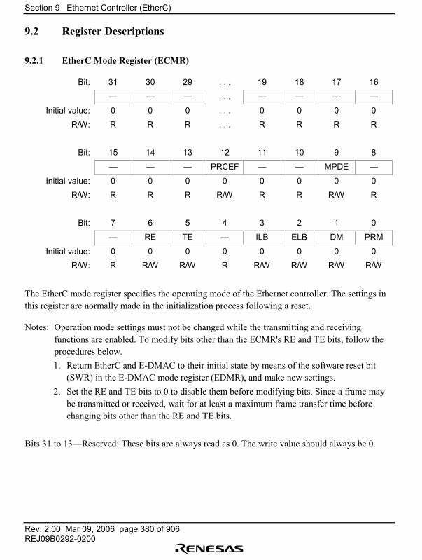
Section 9 Ethernet Controller (EtherC)
Rev. 2.00 Mar 09, 2006 page 380 of 906REJ09B0292-0200
9.2 Register Descriptions
9.2.1 EtherC Mode Register (ECMR)
Bit: 31 30 29 . . . 19 18 17 16
� � � . . . � � � �
Initial value: 0 0 0 . . . 0 0 0 0
R/W: R R R . . . R R R R
Bit: 15 14 13 12 11 10 9 8
� � � PRCEF � � MPDE �
Initial value: 0 0 0 0 0 0 0 0
R/W: R R R R/W R R R/W R
Bit: 7 6 5 4 3 2 1 0
� RE TE � ILB ELB DM PRM
Initial value: 0 0 0 0 0 0 0 0
R/W: R R/W R/W R R/W R/W R/W R/W
The EtherC mode register specifies the operating mode of the Ethernet controller. The settings inthis register are normally made in the initialization process following a reset.
Notes: Operation mode settings must not be changed while the transmitting and receivingfunctions are enabled. To modify bits other than the ECMR's RE and TE bits, follow theprocedures below.1. Return EtherC and E-DMAC to their initial state by means of the software reset bit
(SWR) in the E-DMAC mode register (EDMR), and make new settings.2. Set the RE and TE bits to 0 to disable them before modifying bits. Since a frame may
be transmitted or received, wait for at least a maximum frame transfer time beforechanging bits other than the RE and TE bits.
Bits 31 to 13�Reserved: These bits are always read as 0. The write value should always be 0.
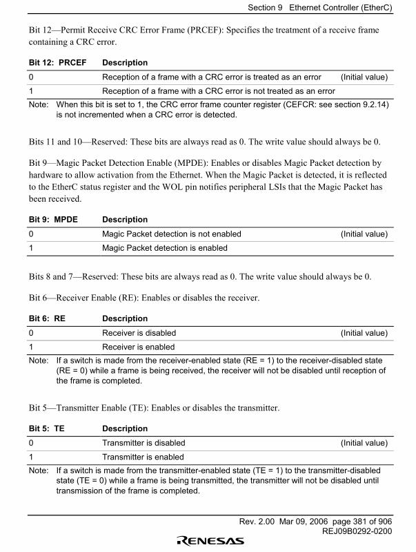
Section 9 Ethernet Controller (EtherC)
Rev. 2.00 Mar 09, 2006 page 381 of 906REJ09B0292-0200
Bit 12�Permit Receive CRC Error Frame (PRCEF): Specifies the treatment of a receive framecontaining a CRC error.
Bit 12: PRCEF Description
0 Reception of a frame with a CRC error is treated as an error (Initial value)
1 Reception of a frame with a CRC error is not treated as an errorNote: When this bit is set to 1, the CRC error frame counter register (CEFCR: see section 9.2.14)
is not incremented when a CRC error is detected.
Bits 11 and 10�Reserved: These bits are always read as 0. The write value should always be 0.
Bit 9�Magic Packet Detection Enable (MPDE): Enables or disables Magic Packet detection byhardware to allow activation from the Ethernet. When the Magic Packet is detected, it is reflectedto the EtherC status register and the WOL pin notifies peripheral LSIs that the Magic Packet hasbeen received.
Bit 9: MPDE Description
0 Magic Packet detection is not enabled (Initial value)
1 Magic Packet detection is enabled
Bits 8 and 7�Reserved: These bits are always read as 0. The write value should always be 0.
Bit 6�Receiver Enable (RE): Enables or disables the receiver.
Bit 6: RE Description
0 Receiver is disabled (Initial value)
1 Receiver is enabledNote: If a switch is made from the receiver-enabled state (RE = 1) to the receiver-disabled state
(RE = 0) while a frame is being received, the receiver will not be disabled until reception ofthe frame is completed.
Bit 5�Transmitter Enable (TE): Enables or disables the transmitter.
Bit 5: TE Description
0 Transmitter is disabled (Initial value)
1 Transmitter is enabledNote: If a switch is made from the transmitter-enabled state (TE = 1) to the transmitter-disabled
state (TE = 0) while a frame is being transmitted, the transmitter will not be disabled untiltransmission of the frame is completed.
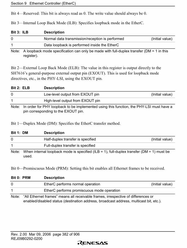
Section 9 Ethernet Controller (EtherC)
Rev. 2.00 Mar 09, 2006 page 382 of 906REJ09B0292-0200
Bit 4�Reserved: This bit is always read as 0. The write value should always be 0.
Bit 3�Internal Loop Back Mode (ILB): Specifies loopback mode in the EtherC.
Bit 3: ILB Description
0 Normal data transmission/reception is performed (Initial value)
1 Data loopback is performed inside the EtherCNote: A loopback mode specification can only be made with full-duplex transfer (DM = 1 in this
register).
Bit 2�External Loop Back Mode (ELB): The value in this register is output directly to theSH7616�s general-purpose external output pin (EXOUT). This is used for loopback modedirectives, etc., in the PHY-LSI, using the EXOUT pin.
Bit 2: ELB Description
0 Low-level output from EXOUT pin (Initial value)
1 High-level output from EXOUT pinNote: In order for PHY loopback to be implemented using this function, the PHY-LSI must have a
pin corresponding to the EXOUT pin.
Bit 1�Duplex Mode (DM): Specifies the EtherC transfer method.
Bit 1: DM Description
0 Half-duplex transfer is specified (Initial value)
1 Full-duplex transfer is specifiedNote: When internal loopback mode is specified (ILB = 1), full-duplex transfer (DM = 1) must be
used.
Bit 0�Promiscuous Mode (PRM): Setting this bit enables all Ethernet frames to be received.
Bit 0: PRM Description
0 EtherC performs normal operation (Initial value)
1 EtherC performs promiscuous mode operationNote: �All Ethernet frames� means all receivable frames, irrespective of differences or
enabled/disabled status (destination address, broadcast address, multicast bit, etc.).
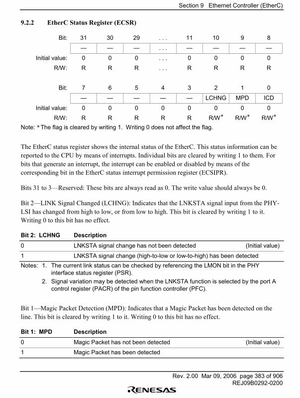
Section 9 Ethernet Controller (EtherC)
Rev. 2.00 Mar 09, 2006 page 383 of 906REJ09B0292-0200
9.2.2 EtherC Status Register (ECSR)
Bit: 31 30 29 . . . 11 10 9 8
� � � . . . � � � �
Initial value: 0 0 0 . . . 0 0 0 0
R/W: R R R . . . R R R R
Bit: 7 6 5 4 3 2 1 0
� � � � � LCHNG MPD ICD
Initial value: 0 0 0 0 0 0 0 0
R/W: R R R R R R/W* R/W* R/W*
Note: * The flag is cleared by writing 1. Writing 0 does not affect the flag.
The EtherC status register shows the internal status of the EtherC. This status information can bereported to the CPU by means of interrupts. Individual bits are cleared by writing 1 to them. Forbits that generate an interrupt, the interrupt can be enabled or disabled by means of thecorresponding bit in the EtherC status interrupt permission register (ECSIPR).
Bits 31 to 3�Reserved: These bits are always read as 0. The write value should always be 0.
Bit 2�LINK Signal Changed (LCHNG): Indicates that the LNKSTA signal input from the PHY-LSI has changed from high to low, or from low to high. This bit is cleared by writing 1 to it.Writing 0 to this bit has no effect.
Bit 2: LCHNG Description
0 LNKSTA signal change has not been detected (Initial value)
1 LNKSTA signal change (high-to-low or low-to-high) has been detectedNotes: 1. The current link status can be checked by referencing the LMON bit in the PHY
interface status register (PSR).2. Signal variation may be detected when the LNKSTA function is selected by the port A
control register (PACR) of the pin function controller (PFC).
Bit 1�Magic Packet Detection (MPD): Indicates that a Magic Packet has been detected on theline. This bit is cleared by writing 1 to it. Writing 0 to this bit has no effect.
Bit 1: MPD Description
0 Magic Packet has not been detected (Initial value)
1 Magic Packet has been detected
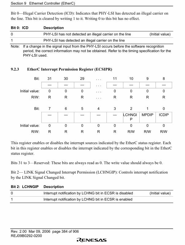
Section 9 Ethernet Controller (EtherC)
Rev. 2.00 Mar 09, 2006 page 384 of 906REJ09B0292-0200
Bit 0�Illegal Carrier Detection (ICD): Indicates that PHY-LSI has detected an illegal carrier onthe line. This bit is cleared by writing 1 to it. Writing 0 to this bit has no effect.
Bit 0: ICD Description
0 PHY-LSI has not detected an illegal carrier on the line (Initial value)
1 PHY-LSI has detected an illegal carrier on the lineNote: If a change in the signal input from the PHY-LSI occurs before the software recognition
period, the correct information may not be obtained. Refer to the timing specification for thePHY-LSI used.
9.2.3 EtherC Interrupt Permission Register (ECSIPR)
Bit: 31 30 29 . . . 11 10 9 8
� � � . . . � � � �
Initial value: 0 0 0 . . . 0 0 0 0
R/W: R R R . . . R R R R
Bit: 7 6 5 4 3 2 1 0
� � � � � LCHNGIP
MPDIP ICDIP
Initial value: 0 0 0 0 0 0 0 0
R/W: R R R R R R/W R/W R/W
This register enables or disables the interrupt sources indicated by the EtherC status register. Eachbit in this register enables or disables the interrupt indicated by the corresponding bit in the EtherCstatus register.
Bits 31 to 3�Reserved: These bits are always read as 0. The write value should always be 0.
Bit 2� LINK Signal Changed Interrupt Permission (LCHNGIP): Controls interrupt notificationby the LINK Signal Changed bit.
Bit 2: LCHNGIP Description
0 Interrupt notification by LCHNG bit in ECSR is disabled (Initial value)
1 Interrupt notification by LCHNG bit in ECSR is enabled
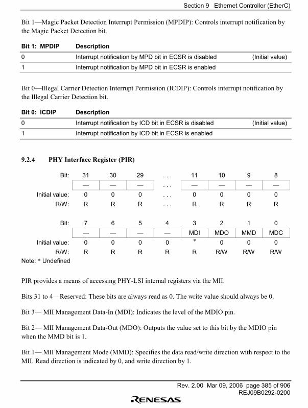
Section 9 Ethernet Controller (EtherC)
Rev. 2.00 Mar 09, 2006 page 385 of 906REJ09B0292-0200
Bit 1�Magic Packet Detection Interrupt Permission (MPDIP): Controls interrupt notification bythe Magic Packet Detection bit.
Bit 1: MPDIP Description
0 Interrupt notification by MPD bit in ECSR is disabled (Initial value)
1 Interrupt notification by MPD bit in ECSR is enabled
Bit 0�Illegal Carrier Detection Interrupt Permission (ICDIP): Controls interrupt notification bythe Illegal Carrier Detection bit.
Bit 0: ICDIP Description
0 Interrupt notification by ICD bit in ECSR is disabled (Initial value)
1 Interrupt notification by ICD bit in ECSR is enabled
9.2.4 PHY Interface Register (PIR)
Bit: 31 30 29 . . . 11 10 9 8� � � . . . � � � �
Initial value: 0 0 0 . . . 0 0 0 0R/W: R R R . . . R R R R
Bit: 7 6 5 4 3 2 1 0� � � � MDI MDO MMD MDC
Initial value: 0 0 0 0 * 0 0 0R/W: R R R R R R/W R/W R/W
Note: * Undefined
PIR provides a means of accessing PHY-LSI internal registers via the MII.
Bits 31 to 4�Reserved: These bits are always read as 0. The write value should always be 0.
Bit 3� MII Management Data-In (MDI): Indicates the level of the MDIO pin.
Bit 2� MII Management Data-Out (MDO): Outputs the value set to this bit by the MDIO pinwhen the MMD bit is 1.
Bit 1� MII Management Mode (MMD): Specifies the data read/write direction with respect to theMII. Read direction is indicated by 0, and write direction by 1.
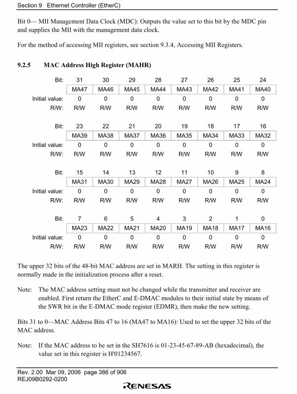
Section 9 Ethernet Controller (EtherC)
Rev. 2.00 Mar 09, 2006 page 386 of 906REJ09B0292-0200
Bit 0� MII Management Data Clock (MDC): Outputs the value set to this bit by the MDC pinand supplies the MII with the management data clock.
For the method of accessing MII registers, see section 9.3.4, Accessing MII Registers.
9.2.5 MAC Address High Register (MAHR)
Bit: 31 30 29 28 27 26 25 24MA47 MA46 MA45 MA44 MA43 MA42 MA41 MA40
Initial value: 0 0 0 0 0 0 0 0R/W: R/W R/W R/W R/W R/W R/W R/W R/W
Bit: 23 22 21 20 19 18 17 16MA39 MA38 MA37 MA36 MA35 MA34 MA33 MA32
Initial value: 0 0 0 0 0 0 0 0R/W: R/W R/W R/W R/W R/W R/W R/W R/W
Bit: 15 14 13 12 11 10 9 8MA31 MA30 MA29 MA28 MA27 MA26 MA25 MA24
Initial value: 0 0 0 0 0 0 0 0R/W: R/W R/W R/W R/W R/W R/W R/W R/W
Bit: 7 6 5 4 3 2 1 0MA23 MA22 MA21 MA20 MA19 MA18 MA17 MA16
Initial value: 0 0 0 0 0 0 0 0R/W: R/W R/W R/W R/W R/W R/W R/W R/W
The upper 32 bits of the 48-bit MAC address are set in MARH. The setting in this register isnormally made in the initialization process after a reset.
Note: The MAC address setting must not be changed while the transmitter and receiver areenabled. First return the EtherC and E-DMAC modules to their initial state by means ofthe SWR bit in the E-DMAC mode register (EDMR), then make the new setting.
Bits 31 to 0�MAC Address Bits 47 to 16 (MA47 to MA16): Used to set the upper 32 bits of theMAC address.
Note: If the MAC address to be set in the SH7616 is 01-23-45-67-89-AB (hexadecimal), thevalue set in this register is H'01234567.
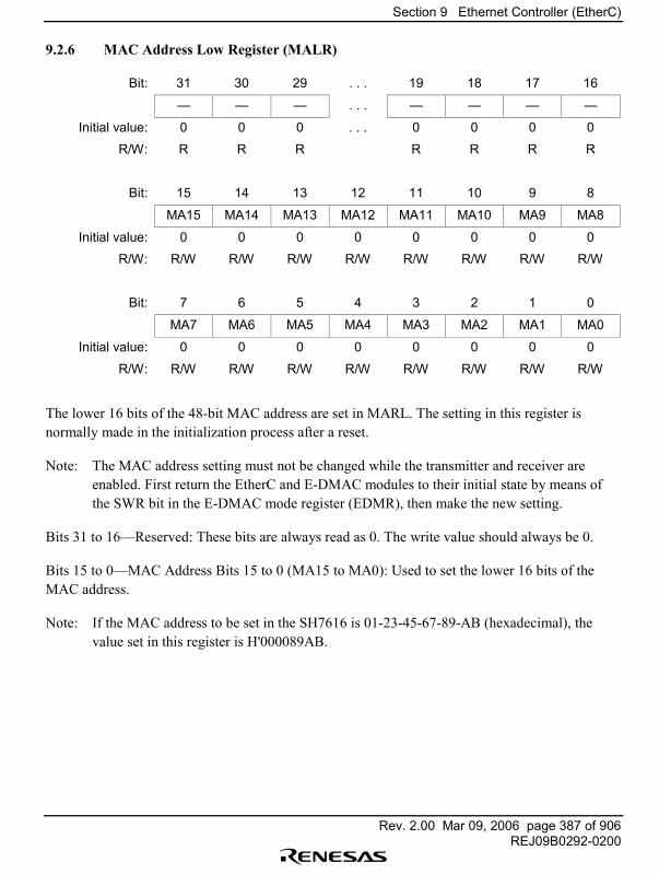
Section 9 Ethernet Controller (EtherC)
Rev. 2.00 Mar 09, 2006 page 387 of 906REJ09B0292-0200
9.2.6 MAC Address Low Register (MALR)
Bit: 31 30 29 . . . 19 18 17 16
� � � . . . � � � �
Initial value: 0 0 0 . . . 0 0 0 0
R/W: R R R R R R R
Bit: 15 14 13 12 11 10 9 8
MA15 MA14 MA13 MA12 MA11 MA10 MA9 MA8
Initial value: 0 0 0 0 0 0 0 0
R/W: R/W R/W R/W R/W R/W R/W R/W R/W
Bit: 7 6 5 4 3 2 1 0
MA7 MA6 MA5 MA4 MA3 MA2 MA1 MA0
Initial value: 0 0 0 0 0 0 0 0
R/W: R/W R/W R/W R/W R/W R/W R/W R/W
The lower 16 bits of the 48-bit MAC address are set in MARL. The setting in this register isnormally made in the initialization process after a reset.
Note: The MAC address setting must not be changed while the transmitter and receiver areenabled. First return the EtherC and E-DMAC modules to their initial state by means ofthe SWR bit in the E-DMAC mode register (EDMR), then make the new setting.
Bits 31 to 16�Reserved: These bits are always read as 0. The write value should always be 0.
Bits 15 to 0�MAC Address Bits 15 to 0 (MA15 to MA0): Used to set the lower 16 bits of theMAC address.
Note: If the MAC address to be set in the SH7616 is 01-23-45-67-89-AB (hexadecimal), thevalue set in this register is H'000089AB.
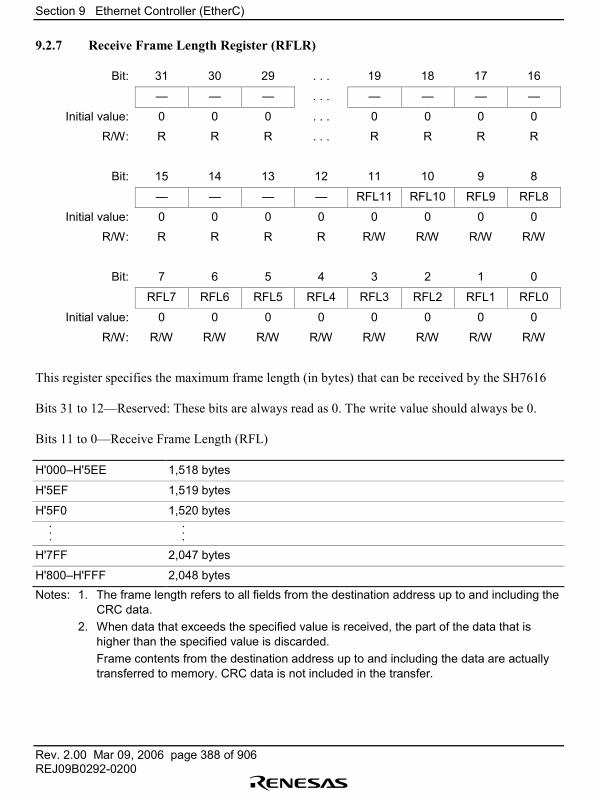
Section 9 Ethernet Controller (EtherC)
Rev. 2.00 Mar 09, 2006 page 388 of 906REJ09B0292-0200
9.2.7 Receive Frame Length Register (RFLR)
Bit: 31 30 29 . . . 19 18 17 16
� � � . . . � � � �
Initial value: 0 0 0 . . . 0 0 0 0
R/W: R R R . . . R R R R
Bit: 15 14 13 12 11 10 9 8
� � � � RFL11 RFL10 RFL9 RFL8
Initial value: 0 0 0 0 0 0 0 0
R/W: R R R R R/W R/W R/W R/W
Bit: 7 6 5 4 3 2 1 0
RFL7 RFL6 RFL5 RFL4 RFL3 RFL2 RFL1 RFL0
Initial value: 0 0 0 0 0 0 0 0
R/W: R/W R/W R/W R/W R/W R/W R/W R/W
This register specifies the maximum frame length (in bytes) that can be received by the SH7616
Bits 31 to 12�Reserved: These bits are always read as 0. The write value should always be 0.
Bits 11 to 0�Receive Frame Length (RFL)
H'000�H'5EE 1,518 bytes
H'5EF 1,519 bytes
H'5F0 1,520 bytes . . .
. . .H'7FF 2,047 bytes
H'800�H'FFF 2,048 bytesNotes: 1. The frame length refers to all fields from the destination address up to and including the
CRC data.2. When data that exceeds the specified value is received, the part of the data that is
higher than the specified value is discarded.Frame contents from the destination address up to and including the data are actuallytransferred to memory. CRC data is not included in the transfer.
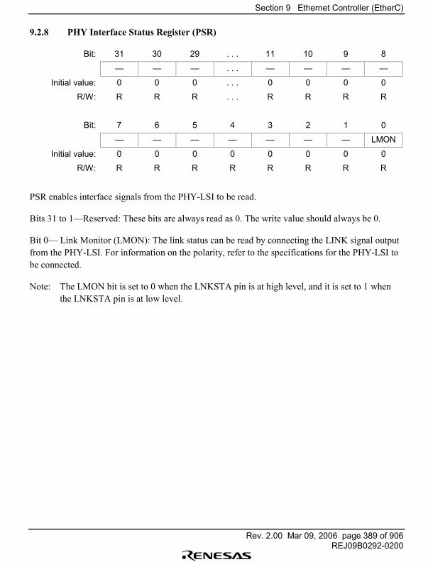
Section 9 Ethernet Controller (EtherC)
Rev. 2.00 Mar 09, 2006 page 389 of 906REJ09B0292-0200
9.2.8 PHY Interface Status Register (PSR)
Bit: 31 30 29 . . . 11 10 9 8
� � � . . . � � � �
Initial value: 0 0 0 . . . 0 0 0 0
R/W: R R R . . . R R R R
Bit: 7 6 5 4 3 2 1 0
� � � � � � � LMON
Initial value: 0 0 0 0 0 0 0 0
R/W: R R R R R R R R
PSR enables interface signals from the PHY-LSI to be read.
Bits 31 to 1�Reserved: These bits are always read as 0. The write value should always be 0.
Bit 0� Link Monitor (LMON): The link status can be read by connecting the LINK signal outputfrom the PHY-LSI. For information on the polarity, refer to the specifications for the PHY-LSI tobe connected.
Note: The LMON bit is set to 0 when the LNKSTA pin is at high level, and it is set to 1 whenthe LNKSTA pin is at low level.
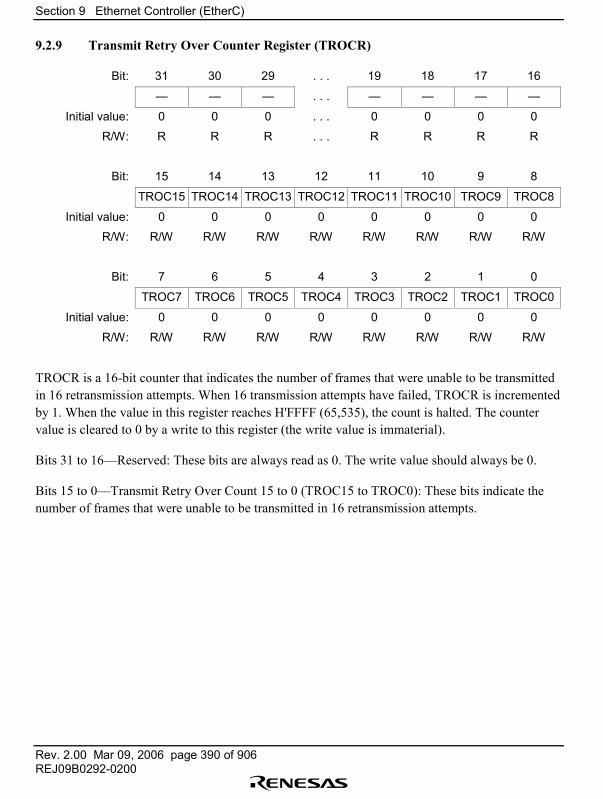
Section 9 Ethernet Controller (EtherC)
Rev. 2.00 Mar 09, 2006 page 390 of 906REJ09B0292-0200
9.2.9 Transmit Retry Over Counter Register (TROCR)
Bit: 31 30 29 . . . 19 18 17 16
� � � . . . � � � �
Initial value: 0 0 0 . . . 0 0 0 0
R/W: R R R . . . R R R R
Bit: 15 14 13 12 11 10 9 8
TROC15 TROC14 TROC13 TROC12 TROC11 TROC10 TROC9 TROC8
Initial value: 0 0 0 0 0 0 0 0
R/W: R/W R/W R/W R/W R/W R/W R/W R/W
Bit: 7 6 5 4 3 2 1 0
TROC7 TROC6 TROC5 TROC4 TROC3 TROC2 TROC1 TROC0
Initial value: 0 0 0 0 0 0 0 0
R/W: R/W R/W R/W R/W R/W R/W R/W R/W
TROCR is a 16-bit counter that indicates the number of frames that were unable to be transmittedin 16 retransmission attempts. When 16 transmission attempts have failed, TROCR is incrementedby 1. When the value in this register reaches H'FFFF (65,535), the count is halted. The countervalue is cleared to 0 by a write to this register (the write value is immaterial).
Bits 31 to 16�Reserved: These bits are always read as 0. The write value should always be 0.
Bits 15 to 0�Transmit Retry Over Count 15 to 0 (TROC15 to TROC0): These bits indicate thenumber of frames that were unable to be transmitted in 16 retransmission attempts.
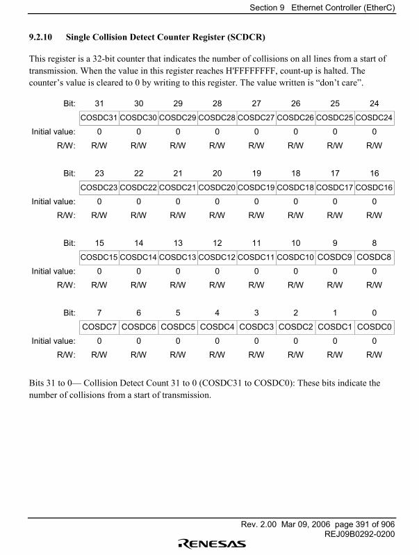
Section 9 Ethernet Controller (EtherC)
Rev. 2.00 Mar 09, 2006 page 391 of 906REJ09B0292-0200
9.2.10 Single Collision Detect Counter Register (SCDCR)
This register is a 32-bit counter that indicates the number of collisions on all lines from a start oftransmission. When the value in this register reaches H'FFFFFFFF, count-up is halted. Thecounter�s value is cleared to 0 by writing to this register. The value written is �don�t care�.
Bit: 31 30 29 28 27 26 25 24
COSDC31 COSDC30 COSDC29 COSDC28 COSDC27 COSDC26 COSDC25 COSDC24
Initial value: 0 0 0 0 0 0 0 0
R/W: R/W R/W R/W R/W R/W R/W R/W R/W
Bit: 23 22 21 20 19 18 17 16
COSDC23 COSDC22 COSDC21 COSDC20 COSDC19 COSDC18 COSDC17 COSDC16
Initial value: 0 0 0 0 0 0 0 0
R/W: R/W R/W R/W R/W R/W R/W R/W R/W
Bit: 15 14 13 12 11 10 9 8
COSDC15 COSDC14 COSDC13 COSDC12 COSDC11 COSDC10 COSDC9 COSDC8
Initial value: 0 0 0 0 0 0 0 0
R/W: R/W R/W R/W R/W R/W R/W R/W R/W
Bit: 7 6 5 4 3 2 1 0
COSDC7 COSDC6 COSDC5 COSDC4 COSDC3 COSDC2 COSDC1 COSDC0
Initial value: 0 0 0 0 0 0 0 0
R/W: R/W R/W R/W R/W R/W R/W R/W R/W
Bits 31 to 0�� Collision Detect Count 31 to 0 (COSDC31 to COSDC0): These bits indicate thenumber of collisions from a start of transmission.
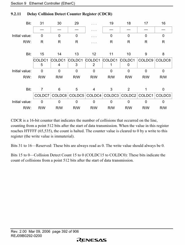
Section 9 Ethernet Controller (EtherC)
Rev. 2.00 Mar 09, 2006 page 392 of 906REJ09B0292-0200
9.2.11 Delay Collision Detect Counter Register (CDCR)
Bit: 31 30 29 . . . 19 18 17 16
� � � . . . � � � �
Initial value: 0 0 0 . . . 0 0 0 0
R/W: R R R . . . R R R R
Bit: 15 14 13 12 11 10 9 8
COLDC15
COLDC14
COLDC13
COLDC12
COLDC11
COLDC10
COLDC9 COLDC8
Initial value: 0 0 0 0 0 0 0 0
R/W: R/W R/W R/W R/W R/W R/W R/W R/W
Bit: 7 6 5 4 3 2 1 0
COLDC7 COLDC6 COLDC5 COLDC4 COLDC3 COLDC2 COLDC1 COLDC0
Initial value: 0 0 0 0 0 0 0 0
R/W: R/W R/W R/W R/W R/W R/W R/W R/W
CDCR is a 16-bit counter that indicates the number of collisions that occurred on the line,counting from a point 512 bits after the start of data transmission. When the value in this registerreaches H'FFFF (65,535), the count is halted. The counter value is cleared to 0 by a write to thisregister (the write value is immaterial).
Bits 31 to 16�Reserved: These bits are always read as 0. The write value should always be 0.
Bits 15 to 0�Collision Detect Count 15 to 0 (COLDC15 to COLDC0): These bits indicate thecount of collisions from a point 512 bits after the start of data transmission.

Section 9 Ethernet Controller (EtherC)
Rev. 2.00 Mar 09, 2006 page 393 of 906REJ09B0292-0200
9.2.12 Lost Carrier Counter Register (LCCR)
Bit: 31 30 29 . . . 19 18 17 16
� � � . . . � � � �
Initial value: 0 0 0 . . . 0 0 0 0
R/W: R R R . . . R R R R
Bit: 15 14 13 12 11 10 9 8
LCC15 LCC14 LCC13 LCC12 LCC11 LCC10 LCC9 LCC8
Initial value: 0 0 0 0 0 0 0 0
R/W: R/W R/W R/W R/W R/W R/W R/W R/W
Bit: 7 6 5 4 3 2 1 0
LCC7 LCC6 LCC5 LCC4 LCC3 LCC2 LCC1 LCC0
Initial value: 0 0 0 0 0 0 0 0
R/W: R/W R/W R/W R/W R/W R/W R/W R/W
LCCR is a 16-bit counter that indicates the number of times the carrier was lost during datatransmission. When the value in this register reaches H'FFFF (65,535), the count is halted. Thecounter value is cleared to 0 by a write to this register (the write value is immaterial).
Bits 31 to 16�Reserved: These bits are always read as 0. The write value should always be 0.
Bits 15 to 0�Lost Carrier Count 15 to 0 (LCC15 to LCC0): These bits indicate the number oftimes the carrier was lost during data transmission.
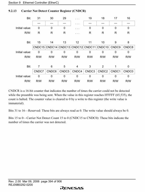
Section 9 Ethernet Controller (EtherC)
Rev. 2.00 Mar 09, 2006 page 394 of 906REJ09B0292-0200
9.2.13 Carrier Not Detect Counter Register (CNDCR)
Bit: 31 30 29 . . . 19 18 17 16
� � � . . . � � � �
Initial value: 0 0 0 . . . 0 0 0 0
R/W: R R R . . . R R R R
Bit: 15 14 13 12 11 10 9 8
CNDC15 CNDC14 CNDC13 CNDC12 CNDC11 CNDC10 CNDC9 CNDC8
Initial value: 0 0 0 0 0 0 0 0
R/W: R/W R/W R/W R/W R/W R/W R/W R/W
Bit: 7 6 5 4 3 2 1 0
CNDC7 CNDC6 CNDC5 CNDC4 CNDC3 CNDC2 CNDC1 CNDC0
Initial value: 0 0 0 0 0 0 0 0
R/W: R/W R/W R/W R/W R/W R/W R/W R/W
CNDCR is a 16-bit counter that indicates the number of times the carrier could not be detectedwhile the preamble was being sent. When the value in this register reaches H'FFFF (65,535), thecount is halted. The counter value is cleared to 0 by a write to this register (the write value isimmaterial).
Bits 31 to 16�Reserved: These bits are always read as 0. The write value should always be 0.
Bits 15 to 0�Carrier Not Detect Count 15 to 0 (CNDC15 to CNDC0): These bits indicate thenumber of times the carrier was not detected.
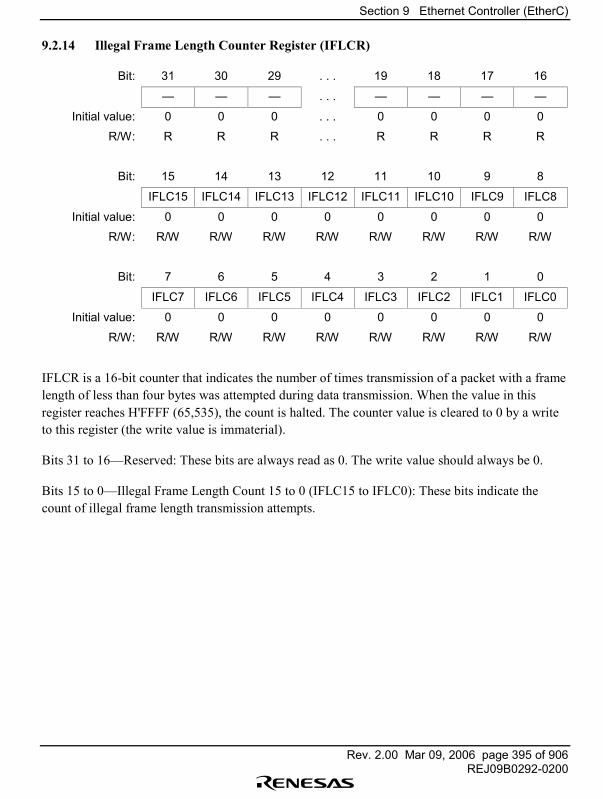
Section 9 Ethernet Controller (EtherC)
Rev. 2.00 Mar 09, 2006 page 395 of 906REJ09B0292-0200
9.2.14 Illegal Frame Length Counter Register (IFLCR)
Bit: 31 30 29 . . . 19 18 17 16
� � � . . . � � � �
Initial value: 0 0 0 . . . 0 0 0 0
R/W: R R R . . . R R R R
Bit: 15 14 13 12 11 10 9 8
IFLC15 IFLC14 IFLC13 IFLC12 IFLC11 IFLC10 IFLC9 IFLC8
Initial value: 0 0 0 0 0 0 0 0
R/W: R/W R/W R/W R/W R/W R/W R/W R/W
Bit: 7 6 5 4 3 2 1 0
IFLC7 IFLC6 IFLC5 IFLC4 IFLC3 IFLC2 IFLC1 IFLC0
Initial value: 0 0 0 0 0 0 0 0
R/W: R/W R/W R/W R/W R/W R/W R/W R/W
IFLCR is a 16-bit counter that indicates the number of times transmission of a packet with a framelength of less than four bytes was attempted during data transmission. When the value in thisregister reaches H'FFFF (65,535), the count is halted. The counter value is cleared to 0 by a writeto this register (the write value is immaterial).
Bits 31 to 16�Reserved: These bits are always read as 0. The write value should always be 0.
Bits 15 to 0�Illegal Frame Length Count 15 to 0 (IFLC15 to IFLC0): These bits indicate thecount of illegal frame length transmission attempts.
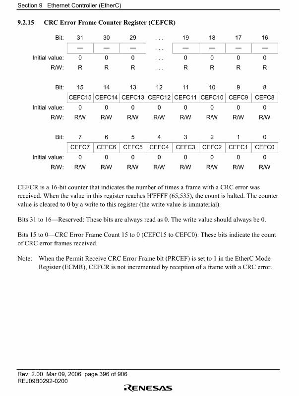
Section 9 Ethernet Controller (EtherC)
Rev. 2.00 Mar 09, 2006 page 396 of 906REJ09B0292-0200
9.2.15 CRC Error Frame Counter Register (CEFCR)
Bit: 31 30 29 . . . 19 18 17 16
� � � . . . � � � �
Initial value: 0 0 0 . . . 0 0 0 0
R/W: R R R . . . R R R R
Bit: 15 14 13 12 11 10 9 8
CEFC15 CEFC14 CEFC13 CEFC12 CEFC11 CEFC10 CEFC9 CEFC8
Initial value: 0 0 0 0 0 0 0 0
R/W: R/W R/W R/W R/W R/W R/W R/W R/W
Bit: 7 6 5 4 3 2 1 0
CEFC7 CEFC6 CEFC5 CEFC4 CEFC3 CEFC2 CEFC1 CEFC0
Initial value: 0 0 0 0 0 0 0 0
R/W: R/W R/W R/W R/W R/W R/W R/W R/W
CEFCR is a 16-bit counter that indicates the number of times a frame with a CRC error wasreceived. When the value in this register reaches H'FFFF (65,535), the count is halted. The countervalue is cleared to 0 by a write to this register (the write value is immaterial).
Bits 31 to 16�Reserved: These bits are always read as 0. The write value should always be 0.
Bits 15 to 0�CRC Error Frame Count 15 to 0 (CEFC15 to CEFC0): These bits indicate the countof CRC error frames received.
Note: When the Permit Receive CRC Error Frame bit (PRCEF) is set to 1 in the EtherC ModeRegister (ECMR), CEFCR is not incremented by reception of a frame with a CRC error.

Section 9 Ethernet Controller (EtherC)
Rev. 2.00 Mar 09, 2006 page 397 of 906REJ09B0292-0200
9.2.16 Frame Receive Error Counter Register (FRECR )
Bit: 31 30 29 . . . 19 18 17 16
� � � . . . � � � �
Initial value: 0 0 0 . . . 0 0 0 0
R/W: R R R . . . R R R R
Bit: 15 14 13 12 11 10 9 8
FREC15 FREC14 FREC13 FREC12 FREC11 FREC10 FREC9 FREC8
Initial value: 0 0 0 0 0 0 0 0
R/W: R/W R/W R/W R/W R/W R/W R/W R/W
Bit: 7 6 5 4 3 2 1 0
FREC7 FREC6 FREC5 FREC4 FREC3 FREC2 FREC1 FREC0
Initial value: 0 0 0 0 0 0 0 0
R/W: R/W R/W R/W R/W R/W R/W R/W R/W
FRECR is a 16-bit counter that indicates the number of frames input from the PHY-LSI for whicha receive error was indicated by the RX-ER pin. FRECR is incremented each time this pinbecomes active. When the value in this register reaches H'FFFF (65,535), the count is halted. Thecounter value is cleared to 0 by a write to this register (the write value is immaterial).
Bits 31 to 16�Reserved: These bits are always read as 0. The write value should always be 0.
Bits 15 to 0�Frame Receive Error Count 15 to 0 (FREC15 to FREC0): These bits indicate thecount of errors during frame reception.
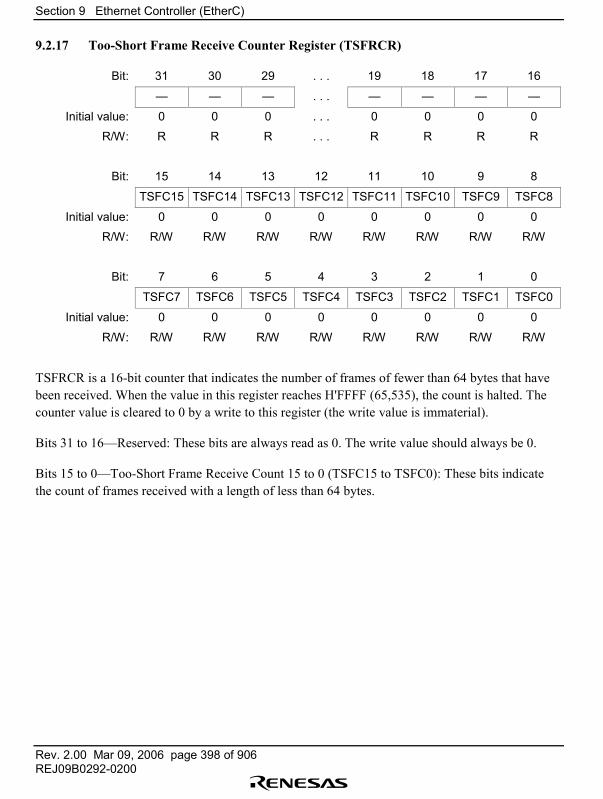
Section 9 Ethernet Controller (EtherC)
Rev. 2.00 Mar 09, 2006 page 398 of 906REJ09B0292-0200
9.2.17 Too-Short Frame Receive Counter Register (TSFRCR)
Bit: 31 30 29 . . . 19 18 17 16
� � � . . . � � � �
Initial value: 0 0 0 . . . 0 0 0 0
R/W: R R R . . . R R R R
Bit: 15 14 13 12 11 10 9 8
TSFC15 TSFC14 TSFC13 TSFC12 TSFC11 TSFC10 TSFC9 TSFC8
Initial value: 0 0 0 0 0 0 0 0
R/W: R/W R/W R/W R/W R/W R/W R/W R/W
Bit: 7 6 5 4 3 2 1 0
TSFC7 TSFC6 TSFC5 TSFC4 TSFC3 TSFC2 TSFC1 TSFC0
Initial value: 0 0 0 0 0 0 0 0
R/W: R/W R/W R/W R/W R/W R/W R/W R/W
TSFRCR is a 16-bit counter that indicates the number of frames of fewer than 64 bytes that havebeen received. When the value in this register reaches H'FFFF (65,535), the count is halted. Thecounter value is cleared to 0 by a write to this register (the write value is immaterial).
Bits 31 to 16�Reserved: These bits are always read as 0. The write value should always be 0.
Bits 15 to 0�Too-Short Frame Receive Count 15 to 0 (TSFC15 to TSFC0): These bits indicatethe count of frames received with a length of less than 64 bytes.

Section 9 Ethernet Controller (EtherC)
Rev. 2.00 Mar 09, 2006 page 399 of 906REJ09B0292-0200
9.2.18 Too-Long Frame Receive Counter Register (TLFRCR)
Bit: 31 30 29 . . . 19 18 17 16
� � � . . . � � � �
Initial value: 0 0 0 . . . 0 0 0 0
R/W: R R R . . . R R R R
Bit: 15 14 13 12 11 10 9 8
TLFC15 TLFC14 TLFC13 TLFC12 TLFC11 TLFC10 TLFC9 TLFC8
Initial value: 0 0 0 0 0 0 0 0
R/W: R/W R/W R/W R/W R/W R/W R/W R/W
Bit: 7 6 5 4 3 2 1 0
TLFC7 TLFC6 TLFC5 TLFC4 TLFC3 TLFC2 TLFC1 TLFC0
Initial value: 0 0 0 0 0 0 0 0
R/W: R/W R/W R/W R/W R/W R/W R/W R/W
TLFRCR is a 16-bit counter that indicates the number of frames received with a length exceedingthe value specified by the receive frame length register (RFLR). When the value in this registerreaches H'FFFF (65,535), the count is halted. The counter value is cleared to 0 by a write to thisregister (the write value is immaterial).
Bits 31 to 16�Reserved: These bits are always read as 0. The write value should always be 0.
Bits 15 to 0�Too-Long Frame Receive Count 15 to 0 (TLFC15 to TLFC0): These bits indicatethe count of frames received with a length exceeding the value in RFLR.
Notes: If the value specified by RFLR is 1518 bytes, TLFRCR is incremented by reception of aframe with a length of 1519 bytes or more.
TLFRCR is not incremented when a frame containing residual bits is received. In thiscase, the reception of the frame is indicated in the residual-bit frame counter register(RFCR).
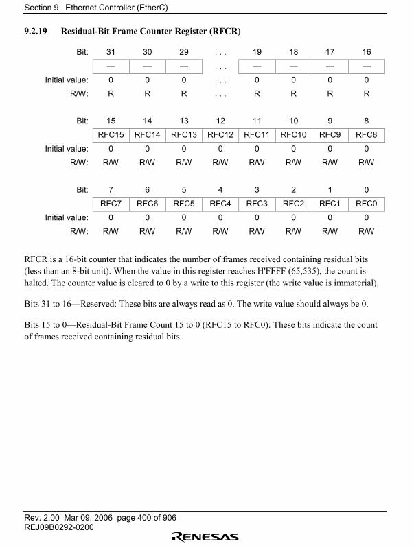
Section 9 Ethernet Controller (EtherC)
Rev. 2.00 Mar 09, 2006 page 400 of 906REJ09B0292-0200
9.2.19 Residual-Bit Frame Counter Register (RFCR)
Bit: 31 30 29 . . . 19 18 17 16
� � � . . . � � � �
Initial value: 0 0 0 . . . 0 0 0 0
R/W: R R R . . . R R R R
Bit: 15 14 13 12 11 10 9 8
RFC15 RFC14 RFC13 RFC12 RFC11 RFC10 RFC9 RFC8
Initial value: 0 0 0 0 0 0 0 0
R/W: R/W R/W R/W R/W R/W R/W R/W R/W
Bit: 7 6 5 4 3 2 1 0
RFC7 RFC6 RFC5 RFC4 RFC3 RFC2 RFC1 RFC0
Initial value: 0 0 0 0 0 0 0 0
R/W: R/W R/W R/W R/W R/W R/W R/W R/W
RFCR is a 16-bit counter that indicates the number of frames received containing residual bits(less than an 8-bit unit). When the value in this register reaches H'FFFF (65,535), the count ishalted. The counter value is cleared to 0 by a write to this register (the write value is immaterial).
Bits 31 to 16�Reserved: These bits are always read as 0. The write value should always be 0.
Bits 15 to 0�Residual-Bit Frame Count 15 to 0 (RFC15 to RFC0): These bits indicate the countof frames received containing residual bits.
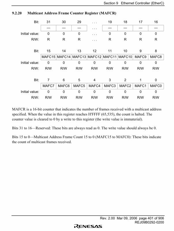
Section 9 Ethernet Controller (EtherC)
Rev. 2.00 Mar 09, 2006 page 401 of 906REJ09B0292-0200
9.2.20 Multicast Address Frame Counter Register (MAFCR)
Bit: 31 30 29 . . . 19 18 17 16
� � � . . . � � � �
Initial value: 0 0 0 . . . 0 0 0 0
R/W: R R R . . . R R R R
Bit: 15 14 13 12 11 10 9 8
MAFC15 MAFC14 MAFC13 MAFC12 MAFC11 MAFC10 MAFC9 MAFC8
Initial value: 0 0 0 0 0 0 0 0
R/W: R/W R/W R/W R/W R/W R/W R/W R/W
Bit: 7 6 5 4 3 2 1 0
MAFC7 MAFC6 MAFC5 MAFC4 MAFC3 MAFC2 MAFC1 MAFC0
Initial value: 0 0 0 0 0 0 0 0
R/W: R/W R/W R/W R/W R/W R/W R/W R/W
MAFCR is a 16-bit counter that indicates the number of frames received with a multicast addressspecified. When the value in this register reaches H'FFFF (65,535), the count is halted. Thecounter value is cleared to 0 by a write to this register (the write value is immaterial).
Bits 31 to 16�Reserved: These bits are always read as 0. The write value should always be 0.
Bits 15 to 0�Multicast Address Frame Count 15 to 0 (MAFC15 to MAFC0): These bits indicatethe count of multicast frames received.
Section 9 Ethernet Controller (EtherC)
Rev. 2.00 Mar 09, 2006 page 402 of 906REJ09B0292-0200
9.3 Operation
When a transmit command is issued from the transmit E-DMAC, the EtherC starts transmission inaccordance with a predetermined transmission procedure. When the specified number of wordshave been transferred, transmission of one frame is terminated.
When an own-address frame (including a broadcast frame) is received, the EtherC transfers theframe to the receive E-DMAC while carrying out format checks. At the end of frame reception theEtherC carries out a CRC check, completing reception of one frame.
Notes: 1. In actual EtherC operation, frame transmission and reception is performedcontinuously in combination with the E-DMACs. For details of continuous operation,see the description of E-DMAC operation.
2. The receive data transferred to memory by the receive data E-DMAC does not includeCRC data.
9.3.1 Transmission
The main transmit functions of the EtherC are as follows:
• Frame generation and transmission: Monitors the line status, then adds the preamble, SFD, andCRC to the data to be transmitted, and sends it to the MII
• CRC generation: Generates the CRC for the data field, and adds it to the transmit frame• Transmission retry: when a collision is detected in the collision window (during the
transmission of the 512-bit data that includes the preamble and SFD from the start oftransmission), transmission is retried up to 15 times based on the back-off algorithm
The state transitions of the EtherC transmitter are shown in figure 9.2.
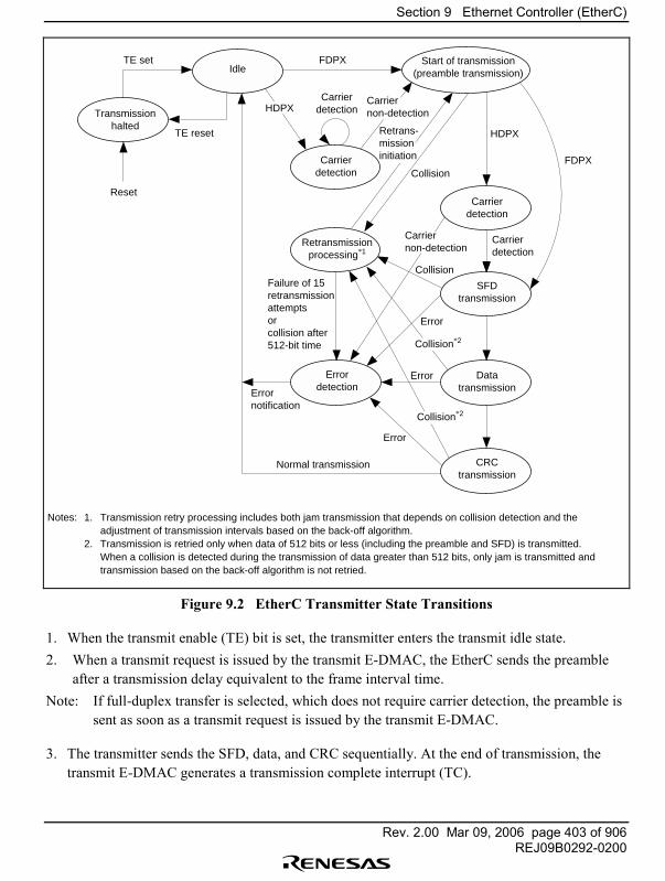
Section 9 Ethernet Controller (EtherC)
Rev. 2.00 Mar 09, 2006 page 403 of 906REJ09B0292-0200
Reset
TE set FDPX
FDPX
TE reset
Failure of 15 retransmission attempts or collision after 512-bit time
Collision
Collision
Normal transmission
Carrierdetection
Carrierdetection
SFDtransmission
Datatransmission
CRCtransmission
Retransmissionprocessing*1
Carrierdetection
Start of transmission(preamble transmission)Idle
Carrier non-detection
Carrier non-detection
Carrierdetection
HDPX
HDPXRetrans-missioninitiation
Transmissionhalted
Errordetection
Error
Error
Error
Error notification
Notes: 1. Transmission retry processing includes both jam transmission that depends on collision detection and the adjustment of transmission intervals based on the back-off algorithm.
2. Transmission is retried only when data of 512 bits or less (including the preamble and SFD) is transmitted. When a collision is detected during the transmission of data greater than 512 bits, only jam is transmitted and
transmission based on the back-off algorithm is not retried.
Collision*2
Collision*2
Figure 9.2 EtherC Transmitter State Transitions
1. When the transmit enable (TE) bit is set, the transmitter enters the transmit idle state.2. When a transmit request is issued by the transmit E-DMAC, the EtherC sends the preamble
after a transmission delay equivalent to the frame interval time.Note: If full-duplex transfer is selected, which does not require carrier detection, the preamble is
sent as soon as a transmit request is issued by the transmit E-DMAC.
3. The transmitter sends the SFD, data, and CRC sequentially. At the end of transmission, thetransmit E-DMAC generates a transmission complete interrupt (TC).
Section 9 Ethernet Controller (EtherC)
Rev. 2.00 Mar 09, 2006 page 404 of 906REJ09B0292-0200
Note: If a collision or the carrier-not-detected state occurs during data transmission, these arereported as interrupt sources.
4. After waiting for the frame interval time, the transmitter enters the idle state, and if there ismore transmit data, continues transmitting.
9.3.2 Reception
The EtherC receiver separates a received frame into preamble, SFD, data, and CRC, and the fieldsfrom DA (destination address) to the CRC data are transferred to the receive E-DMAC. The mainreceive functions of the EtherC are as follows:
• Receive frame header check: Checks the preamble and SFD, and discards a frame with aninvalid pattern
• Receive frame data check: Checks the data length in the header, and reports an error status ifthe data length is less than 64 bytes or greater than the specified number of bytes
• Receive CRC check: Performs a CRC check on the frame data field, and reports an error statusin the case of an abnormality
• Line status monitoring: Reports an error status if an illegal carrier is detected by means of thefault detection signal from the PHY-LSI
• Magic Packet monitoring: Detects a Magic Packet from all receive frames
The state transitions of the EtherC receiver are shown in figure 9.3.
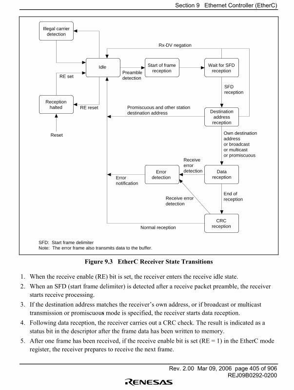
Section 9 Ethernet Controller (EtherC)
Rev. 2.00 Mar 09, 2006 page 405 of 906REJ09B0292-0200
Reset
RE set
RE reset
SFD: Start frame delimiter Note: The error frame also transmits data to the buffer.
Preamble detection
Rx-DV negation
Promiscuous and other station destination address
SFD reception
Own destination addressor broadcast or multicastor promiscuous
End of reception
Error notification
Receive error detection
Receive error detection
Normal reception
Receptionhalted
Illegal carrierdetection
Idle Start of framereception
Destinationaddress
reception
Errordetection
Datareception
CRCreception
Wait for SFDreception
Figure 9.3 EtherC Receiver State Transitions
1. When the receive enable (RE) bit is set, the receiver enters the receive idle state.2. When an SFD (start frame delimiter) is detected after a receive packet preamble, the receiver
starts receive processing.3. If the destination address matches the receiver�s own address, or if broadcast or multicast
transmission or promiscuous mode is specified, the receiver starts data reception.4. Following data reception, the receiver carries out a CRC check. The result is indicated as a
status bit in the descriptor after the frame data has been written to memory.5. After one frame has been received, if the receive enable bit is set (RE = 1) in the EtherC mode
register, the receiver prepares to receive the next frame.
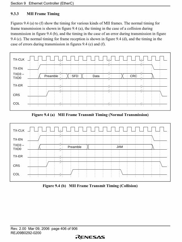
Section 9 Ethernet Controller (EtherC)
Rev. 2.00 Mar 09, 2006 page 406 of 906REJ09B0292-0200
9.3.3 MII Frame Timing
Figures 9.4 (a) to (f) show the timing for various kinds of MII frames. The normal timing forframe transmission is shown in figure 9.4 (a), the timing in the case of a collision duringtransmission in figure 9.4 (b), and the timing in the case of an error during transmission in figure9.4 (c). The normal timing for frame reception is shown in figure 9.4 (d), and the timing in thecase of errors during transmission in figures 9.4 (e) and (f).
TX-CLK
TX-EN
TXD3 –TXD0
TX-ER
CRS
COL
SFDPreamble Data CRC
Figure 9.4 (a) MII Frame Transmit Timing (Normal Transmission)
TX-CLK
TX-EN
TXD3 –TXD0
TX-ER
CRS
COL
Preamble JAM
Figure 9.4 (b) MII Frame Transmit Timing (Collision)
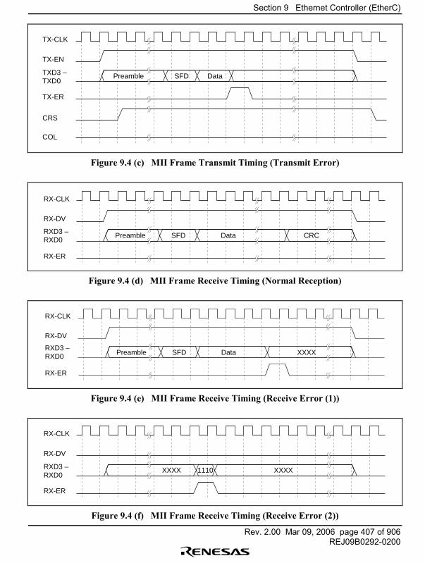
Section 9 Ethernet Controller (EtherC)
Rev. 2.00 Mar 09, 2006 page 407 of 906REJ09B0292-0200
TX-CLK
TX-EN
TXD3 –TXD0
TX-ER
CRS
COL
SFDPreamble Data
Figure 9.4 (c) MII Frame Transmit Timing (Transmit Error)
RX-CLK
RX-DV
RXD3 –RXD0
RX-ER
Preamble Data CRCSFD
Figure 9.4 (d) MII Frame Receive Timing (Normal Reception)
RX-CLK
RX-DV
RXD3 –RXD0
RX-ER
Preamble Data XXXXSFD
Figure 9.4 (e) MII Frame Receive Timing (Receive Error (1))
RX-CLK
RX-DV
RXD3 –RXD0
RX-ER
XXXX 1110 XXXX
Figure 9.4 (f) MII Frame Receive Timing (Receive Error (2))
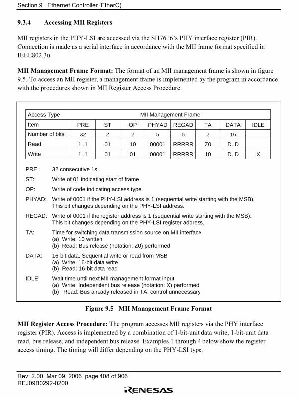
Section 9 Ethernet Controller (EtherC)
Rev. 2.00 Mar 09, 2006 page 408 of 906REJ09B0292-0200
9.3.4 Accessing MII Registers
MII registers in the PHY-LSI are accessed via the SH7616�s PHY interface register (PIR).Connection is made as a serial interface in accordance with the MII frame format specified inIEEE802.3u.
MII Management Frame Format: The format of an MII management frame is shown in figure9.5. To access an MII register, a management frame is implemented by the program in accordancewith the procedures shown in MII Register Access Procedure.
Access Type MII Management Frame
Item
Number of bits
Read
Write
PRE
32
1..1
1..1
ST
2
01
01
OP
2
10
01
PHYAD
5
00001
00001
REGAD
5
RRRRR
RRRRR
TA
2
Z0
10
DATA
16
D..D
D..D
IDLE
X
PRE: 32 consecutive 1s
ST: Write of 01 indicating start of frame
OP: Write of code indicating access type
PHYAD: Write of 0001 if the PHY-LSI address is 1 (sequential write starting with the MSB). This bit changes depending on the PHY-LSI address.
REGAD: Write of 0001 if the register address is 1 (sequential write starting with the MSB). This bit changes depending on the PHY-LSI register address.
TA: Time for switching data transmission source on MII interface (a) Write: 10 written (b) Read: Bus release (notation: Z0) performed
DATA: 16-bit data. Sequential write or read from MSB (a) Write: 16-bit data write (b) Read: 16-bit data read
IDLE: Wait time until next MII management format input (a) Write: Independent bus release (notation: X) performed (b) Read: Bus already released in TA; control unnecessary
Figure 9.5 MII Management Frame Format
MII Register Access Procedure: The program accesses MII registers via the PHY interfaceregister (PIR). Access is implemented by a combination of 1-bit-unit data write, 1-bit-unit dataread, bus release, and independent bus release. Examples 1 through 4 below show the registeraccess timing. The timing will differ depending on the PHY-LSI type.
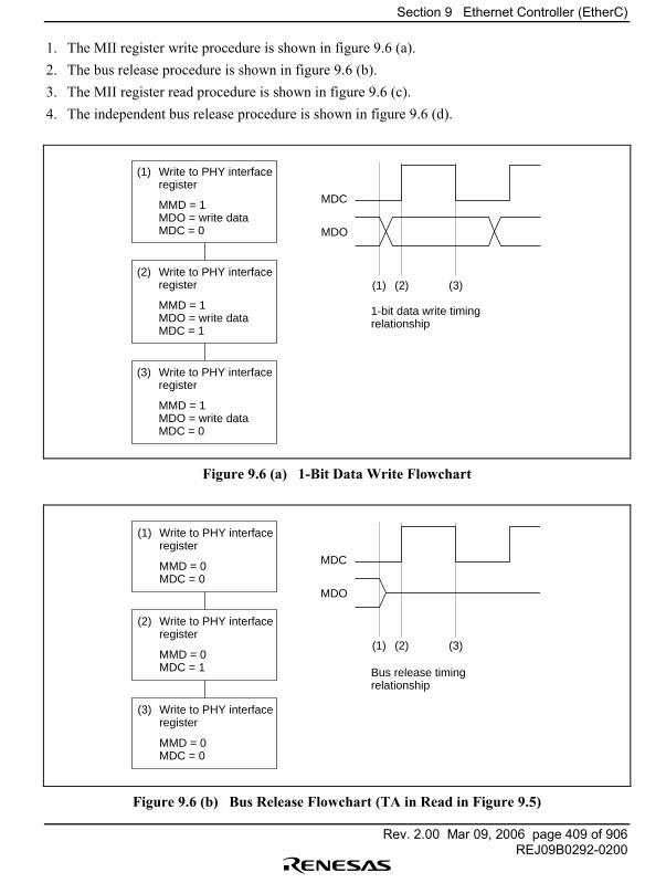
Section 9 Ethernet Controller (EtherC)
Rev. 2.00 Mar 09, 2006 page 409 of 906REJ09B0292-0200
1. The MII register write procedure is shown in figure 9.6 (a).2. The bus release procedure is shown in figure 9.6 (b).3. The MII register read procedure is shown in figure 9.6 (c).4. The independent bus release procedure is shown in figure 9.6 (d).
MDC
MDO
1-bit data write timing relationship
(1) Write to PHY interface register
MMD = 1 MDO = write data MDC = 0
(2) Write to PHY interface register
MMD = 1 MDO = write data MDC = 1
(3) Write to PHY interface register
MMD = 1 MDO = write data MDC = 0
(1) (2) (3)
Figure 9.6 (a) 1-Bit Data Write Flowchart
MDC
MDO
Bus release timing relationship
(1) Write to PHY interface register
MMD = 0 MDC = 0
(2) Write to PHY interface register
MMD = 0 MDC = 1
(3) Write to PHY interface register
MMD = 0 MDC = 0
(1) (2) (3)
Figure 9.6 (b) Bus Release Flowchart (TA in Read in Figure 9.5)
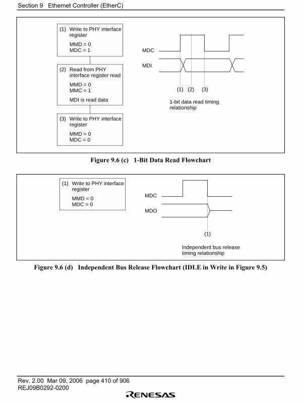
Section 9 Ethernet Controller (EtherC)
Rev. 2.00 Mar 09, 2006 page 410 of 906REJ09B0292-0200
1-bit data read timing relationship
(1) Write to PHY interface register
MMD = 0 MDC = 1
(2) Read from PHY interface register read
MMD = 0 MMC = 1
MDI is read data
(3) Write to PHY interface register
MMD = 0 MDC = 0
MDC
MDI
(1) (3)(2)
Figure 9.6 (c) 1-Bit Data Read Flowchart
Independent bus release timing relationship
(1) Write to PHY interface register
MMD = 0 MDC = 0
MDC
MDO
(1)
Figure 9.6 (d) Independent Bus Release Flowchart (IDLE in Write in Figure 9.5)

Section 9 Ethernet Controller (EtherC)
Rev. 2.00 Mar 09, 2006 page 411 of 906REJ09B0292-0200
9.3.5 Magic Packet Detection
The EtherC has a Magic Packet detection function. This function provides a Wake-On-LAN(WOL) facility that activates various peripheral devices connected to a LAN from the host deviceor other source. This makes it possible to construct a system in which a peripheral device receivesa Magic Packet sent from the host device or other source, and activates itself. Further informationon Magic Packets can be found in the technical documentation published by AMD Corporation.
The procedure for using the WOL function with the SH7616 is as follows.
1. Disable interrupt source output by means of the various interrupt enable/mask registers.2. Set the Magic Packet detection enable bit (MPDE) in the EtherC mode register (ECMR).3. Set the Magic Packet detection interrupt enable bit (MPDIP) in the EtherC interrupt enable
register (ECSIPR) to the enable setting.4. If necessary, set the CPU operating mode to sleep mode or set supporting functions to module
standby mode.5. When a Magic Packet is detected, an interrupt is sent to the CPU. The WOL pin notifies
peripheral LSIs that the Magic Packet has been detected.
Notes: 1. When the Magic Packet is detected, data is stored in the receive FIFO by the broadcastpacket that has received data previously and the EtherC is notified of the receivingstatus. To return to normal operation from the interrupt processing, initialize the EtherCand E-DMAC by using the software reset bit (SWR) in the E-DMAC mode register(EDMR).
2. With a Magic Packet, reception is performed regardless of the destination address. As aresult, this function is valid, and the WOL pin enabled, only in the case of a match withthe destination address specified by the format in the Magic Packet.
Section 9 Ethernet Controller (EtherC)
Rev. 2.00 Mar 09, 2006 page 412 of 906REJ09B0292-0200
9.3.6 CPU Operating Mode and Ethernet Controller Operation
The SH7616 enables a low-power-consumption system to be constructed by selecting orcombining three functions: a module standby function that halts the operation of unnecessary on-chip modules, a sleep mode that halts CPU functions, and a standby function that halts all thechip�s functions. Details of each operating mode are given in section 21, Power-Down State. Here,features and points for attention when these functions are used in combination with the Ethernetcontroller are described.
Sleep Mode: In sleep mode, the operation of the CPU and DSP is halted. The EtherC, on-chipsupporting functions, and external pins continue to operate. Recovery from sleep mode can becarried out by means of an interrupt from the EtherC or a supporting module, or a reset. In order tocontrol external pins and the WOL pin by means of Magic Packet reception, the relevant pins mustbe set beforehand.
Note: In order to specify recovery by means of a magic packet, supporting function interruptsources should be masked before sleep mode is entered. See section 9.3.5, Magic PacketDetection, for the setting procedure.
Standby Mode: In standby mode, the on-chip oscillation circuit is halted. Consequently, the clockis not supplied to the EtherC, and interrupts from the EtherC and other supporting modules cannotbe reported. It is therefore not possible to restore normal operation by these means, and so theWOL function cannot be used.
Notes: This mode can be selected to halt all functions including the EtherC. However, an NMIinterrupt, power-on reset, or manual reset is necessary in order to restore normal operation.
When the SH7616 has been placed in standby mode, the CPU, DSP, and bus statecontroller are among the functions halted. When DRAM is connected, refreshing is alsohalted, and therefore initialization of memory, etc., is necessary after recovery, in the sameway as in a reset.
Module Standby Mode: Module standby mode allows individual supporting modules to be run orhalted. However, due to the nature of its function, the operation of the EtherC cannot be stopped.During normal operation, module standby mode can be used to halt unnecessary supportingfunctions. The CPU and DSP continue to operate in this mode.
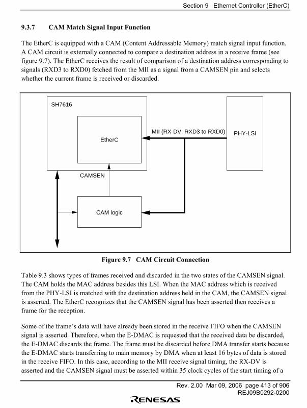
Section 9 Ethernet Controller (EtherC)
Rev. 2.00 Mar 09, 2006 page 413 of 906REJ09B0292-0200
9.3.7 CAM Match Signal Input Function
The EtherC is equipped with a CAM (Content Addressable Memory) match signal input function.A CAM circuit is externally connected to compare a destination address in a receive frame (seefigure 9.7). The EtherC receives the result of comparison of a destination address corresponding tosignals (RXD3 to RXD0) fetched from the MII as a signal from a CAMSEN pin and selectswhether the current frame is received or discarded.
SH7616
EtherC
CAMSEN
CAM logic
MII (RX-DV, RXD3 to RXD0) PHY-LSI
Figure 9.7 CAM Circuit Connection
Table 9.3 shows types of frames received and discarded in the two states of the CAMSEN signal.The CAM holds the MAC address besides this LSI. When the MAC address which is receivedfrom the PHY-LSI is matched with the destination address held in the CAM, the CAMSEN signalis asserted. The EtherC recognizes that the CAMSEN signal has been asserted then receives aframe for the reception.
Some of the frame�s data will have already been stored in the receive FIFO when the CAMSENsignal is asserted. Therefore, when the E-DMAC is requested that the received data be discarded,the E-DMAC discards the frame. The frame must be discarded before DMA transfer starts becausethe E-DMAC starts transferring to main memory by DMA when at least 16 bytes of data is storedin the receive FIFO. In this case, according to the MII receive signal timing, the RX-DV isasserted and the CAMSEN signal must be asserted within 35 clock cycles of the start timing of a
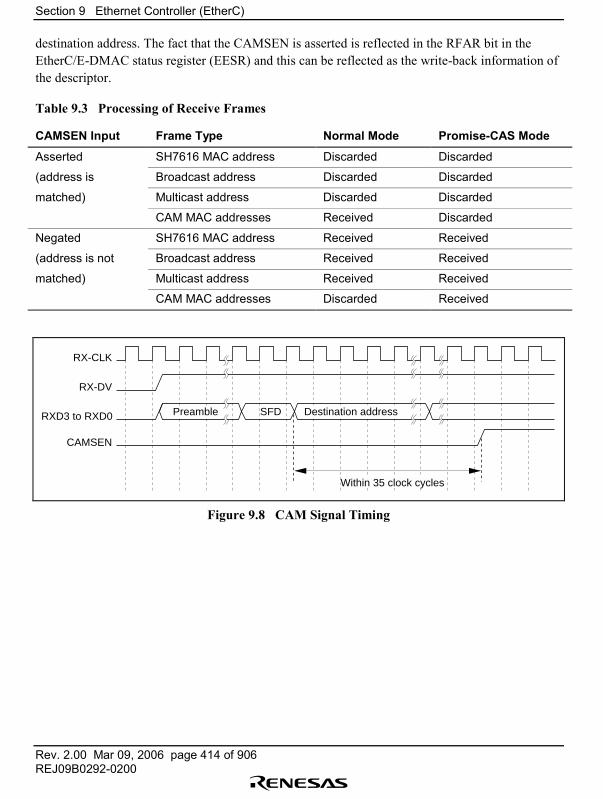
Section 9 Ethernet Controller (EtherC)
Rev. 2.00 Mar 09, 2006 page 414 of 906REJ09B0292-0200
destination address. The fact that the CAMSEN is asserted is reflected in the RFAR bit in theEtherC/E-DMAC status register (EESR) and this can be reflected as the write-back information ofthe descriptor.
Table 9.3 Processing of Receive Frames
CAMSEN Input Frame Type Normal Mode Promise-CAS Mode
Asserted SH7616 MAC address Discarded Discarded
(address is Broadcast address Discarded Discarded
matched) Multicast address Discarded Discarded
CAM MAC addresses Received Discarded
Negated SH7616 MAC address Received Received
(address is not Broadcast address Received Received
matched) Multicast address Received Received
CAM MAC addresses Discarded Received
RX-CLK
RX-DV
RXD3 to RXD0
CAMSEN
SFDPreamble Destination address
Within 35 clock cycles
Figure 9.8 CAM Signal Timing
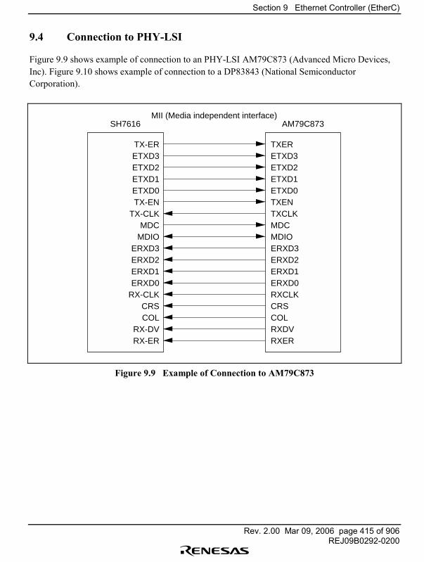
Section 9 Ethernet Controller (EtherC)
Rev. 2.00 Mar 09, 2006 page 415 of 906REJ09B0292-0200
9.4 Connection to PHY-LSI
Figure 9.9 shows example of connection to an PHY-LSI AM79C873 (Advanced Micro Devices,Inc). Figure 9.10 shows example of connection to a DP83843 (National SemiconductorCorporation).
TX-ERETXD3ETXD2ETXD1ETXD0TX-EN
TX-CLKMDC
MDIOERXD3ERXD2ERXD1ERXD0
RX-CLKCRSCOL
RX-DVRX-ER
TXERETXD3ETXD2ETXD1ETXD0TXENTXCLKMDCMDIOERXD3ERXD2ERXD1ERXD0RXCLKCRSCOLRXDVRXER
SH7616 AM79C873MII (Media independent interface)
Figure 9.9 Example of Connection to AM79C873
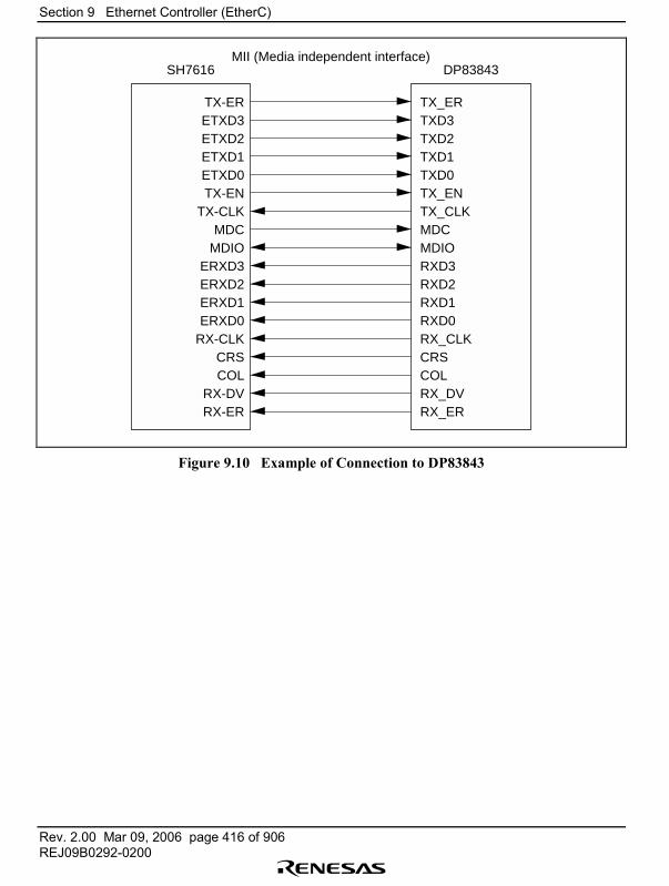
Section 9 Ethernet Controller (EtherC)
Rev. 2.00 Mar 09, 2006 page 416 of 906REJ09B0292-0200
TX-ERETXD3ETXD2ETXD1ETXD0TX-EN
TX-CLKMDC
MDIOERXD3ERXD2ERXD1ERXD0
RX-CLKCRSCOL
RX-DVRX-ER
TX_ERTXD3TXD2TXD1TXD0TX_ENTX_CLKMDCMDIORXD3RXD2RXD1RXD0RX_CLKCRSCOLRX_DVRX_ER
SH7616 DP83843MII (Media independent interface)
Figure 9.10 Example of Connection to DP83843
Section 10 Ethernet Controller Direct Memory Access Controller (E-DMAC)
Rev. 2.00 Mar 09, 2006 page 417 of 906REJ09B0292-0200
Section 10 Ethernet Controller Direct Memory AccessController (E-DMAC)
10.1 Overview
The SH7616 has an on-chip two-channel direct memory access controller (E-DMAC) directlyconnected to the Ethernet controller (EtherC). A large proportion of buffer management iscontrolled by the E-DMAC itself using descriptors. This lightens the load on the CPU and enablesefficient data transfer control to be achieved.
10.1.1 Features
The E-DMAC has the following features:
• The load on the CPU is reduced by means of a descriptor management system• Transmit/receive frame status information is indicated in descriptors• Achieves efficient system bus utilization through the use of block transfer (16-byte units)• Supports single-frame/multi-buffer operation
Note: The E-DMAC cannot access peripheral modules.

Section 10 Ethernet Controller Direct Memory Access Controller (E-DMAC)
Rev. 2.00 Mar 09, 2006 page 418 of 906REJ09B0292-0200
10.1.2 Configuration
Figure 10.1 shows the configuration of the E-DMAC, and the descriptors and transmit/receivebuffers in memory.
SH7616 E-DMAC
Internalbus
interface EtherC
Descriptorinformation
Transmit DMAC
Descriptorinformation
Receive DMAC
External bus interface
Tx FIFO
Rx FIFO
Transmitdescriptors
Transmitbuffer
Receivedescriptors
Receivebuffer
Memory
Figure 10.1 Configuration of E-DMAC, and Descriptors and Buffers
Section 10 Ethernet Controller Direct Memory Access Controller (E-DMAC)
Rev. 2.00 Mar 09, 2006 page 419 of 906REJ09B0292-0200
10.1.3 Descriptor Management System
The E-DMAC manages the transmit/receive buffers by means of corresponding transmit/receivedescriptor lists.
Transmission: The transmit E-DMAC fetches a transmit buffer address from the top of thetransmit descriptor list, and transfers the transmit data in the buffer to the transmit FIFO. If atransmit directive follows in the descriptor, the E-DMAC reads the next descriptor and transfersthe data in the corresponding buffer to the transmit FIFO. In this way, continuous datatransmission can be carried out.
Reception: For each start of a receive DMA transfer, the receive E-DMAC fetches a receivebuffer address from the top of the receive descriptor list. When receive data is stored in the receiveFIFO, the E-DMAC transfers this data to the receive buffer. When reception of one frame isfinished, the E-DMAC performs a receive status write and fetches the receive buffer address fromthe next descriptor. By repeating this sequence, consecutive frames can be received.
10.1.4 Register Configuration
The E-DMAC has the seventeen 32-bit registers shown in table 10.1.
Notes: 1. All registers must be accessed as 32-bit units.2. Reserved bits in a register should only be written with 0.3. The value read from a reserved bit is not guaranteed.
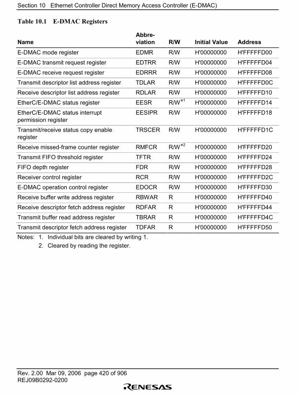
Section 10 Ethernet Controller Direct Memory Access Controller (E-DMAC)
Rev. 2.00 Mar 09, 2006 page 420 of 906REJ09B0292-0200
Table 10.1 E-DMAC Registers
NameAbbre-viation R/W Initial Value Address
E-DMAC mode register EDMR R/W H'00000000 H'FFFFFD00
E-DMAC transmit request register EDTRR R/W H'00000000 H'FFFFFD04
E-DMAC receive request register EDRRR R/W H'00000000 H'FFFFFD08
Transmit descriptor list address register TDLAR R/W H'00000000 H'FFFFFD0C
Receive descriptor list address register RDLAR R/W H'00000000 H'FFFFFD10
EtherC/E-DMAC status register EESR R/W*1 H'00000000 H'FFFFFD14
EtherC/E-DMAC status interruptpermission register
EESIPR R/W H'00000000 H'FFFFFD18
Transmit/receive status copy enableregister
TRSCER R/W H'00000000 H'FFFFFD1C
Receive missed-frame counter register RMFCR R/W*2 H'00000000 H'FFFFFD20
Transmit FIFO threshold register TFTR R/W H'00000000 H'FFFFFD24
FIFO depth register FDR R/W H'00000000 H'FFFFFD28
Receiver control register RCR R/W H'00000000 H'FFFFFD2C
E-DMAC operation control register EDOCR R/W H'00000000 H'FFFFFD30
Receive buffer write address register RBWAR R H'00000000 H'FFFFFD40
Receive descriptor fetch address register RDFAR R H'00000000 H'FFFFFD44
Transmit buffer read address register TBRAR R H'00000000 H'FFFFFD4C
Transmit descriptor fetch address register TDFAR R H'00000000 H'FFFFFD50Notes: 1. Individual bits are cleared by writing 1.
2. Cleared by reading the register.
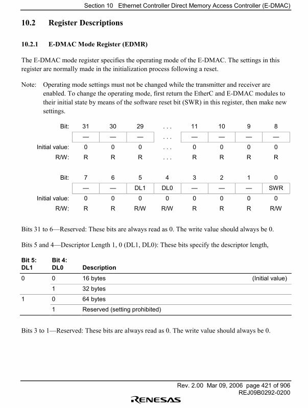
Section 10 Ethernet Controller Direct Memory Access Controller (E-DMAC)
Rev. 2.00 Mar 09, 2006 page 421 of 906REJ09B0292-0200
10.2 Register Descriptions
10.2.1 E-DMAC Mode Register (EDMR)
The E-DMAC mode register specifies the operating mode of the E-DMAC. The settings in thisregister are normally made in the initialization process following a reset.
Note: Operating mode settings must not be changed while the transmitter and receiver areenabled. To change the operating mode, first return the EtherC and E-DMAC modules totheir initial state by means of the software reset bit (SWR) in this register, then make newsettings.
Bit: 31 30 29 . . . 11 10 9 8
� � � . . . � � � �
Initial value: 0 0 0 . . . 0 0 0 0
R/W: R R R . . . R R R R
Bit: 7 6 5 4 3 2 1 0
� � DL1 DL0 � � � SWR
Initial value: 0 0 0 0 0 0 0 0
R/W: R R R/W R/W R R R R/W
Bits 31 to 6�Reserved: These bits are always read as 0. The write value should always be 0.
Bits 5 and 4�Descriptor Length 1, 0 (DL1, DL0): These bits specify the descriptor length,
Bit 5:DL1
Bit 4:DL0 Description
0 0 16 bytes (Initial value)
1 32 bytes
1 0 64 bytes
1 Reserved (setting prohibited)
Bits 3 to 1�Reserved: These bits are always read as 0. The write value should always be 0.
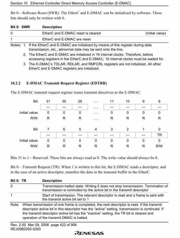
Section 10 Ethernet Controller Direct Memory Access Controller (E-DMAC)
Rev. 2.00 Mar 09, 2006 page 422 of 906REJ09B0292-0200
Bit 0�Software Reset (SWR): The EtherC and E-DMAC can be initialized by software. Thesebits should only be written with 0.
Bit 0: SWR Description
0 EtherC and E-DMAC reset is cleared (Initial value)
1 EtherC and E-DMAC are resetNotes: 1. If the EtherC and E-DMAC are initialized by means of this register during data
transmission, etc., abnormal data may be sent onto the line.2. The EtherC and E-DMAC are initialized in 16 internal clocks. Therefore, before
accessing registers in the EtherC and E-DMAC, 16 internal clocks must be waited for.3. The E-DMAC�s TDLAR, RDLAR, and RMFCRL registers are not initialized. All other
EtherC and E-DMAC registers are initialized.
10.2.2 E-DMAC Transmit Request Register (EDTRR)
The E-DMAC transmit request register issues transmit directives to the E-DMAC.
Bit: 31 30 29 . . . 11 10 9 8� � � . . . � � � �
Initial value: 0 0 0 . . . 0 0 0 0R/W: R R R . . . R R R R
Bit: 7 6 5 4 3 2 1 0� � � � � � � TR
Initial value: 0 0 0 0 0 0 0 0R/W: R R R R R R R R/W
Bits 31 to 1�Reserved: These bits are always read as 0. The write value should always be 0.
Bit 0�Transmit Request (TR): When 1 is written to this bit, the E-DMAC reads a descriptor, andin the case of an active descriptor, transfers the data in the transmit buffer to the EtherC.
Bit 0: TR Description0 Transmission-halted state. Writing 0 does not stop transmission. Termination of
transmission is controlled by the active bit in the transmit descriptor1 Start of transmission. The relevant descriptor is read and a frame is sent with
the transmit active bit set to 1Note: When transmission of one frame is completed, the next descriptor is read. If the transmit
descriptor active bit in this descriptor has the �active� setting, transmission is continued. Ifthe transmit descriptor active bit has the �inactive� setting, the TR bit is cleared andoperation of the transmit DMAC is halted.
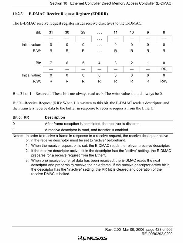
Section 10 Ethernet Controller Direct Memory Access Controller (E-DMAC)
Rev. 2.00 Mar 09, 2006 page 423 of 906REJ09B0292-0200
10.2.3 E-DMAC Receive Request Register (EDRRR)
The E-DMAC receive request register issues receive directives to the E-DMAC.
Bit: 31 30 29 . . . 11 10 9 8
� � � . . . � � � �
Initial value: 0 0 0 . . . 0 0 0 0
R/W: R R R . . . R R R R
Bit: 7 6 5 4 3 2 1 0
� � � � � � � RR
Initial value: 0 0 0 0 0 0 0 0
R/W: R R R R R R R R/W
Bits 31 to 1�Reserved: These bits are always read as 0. The write value should always be 0.
Bit 0�Receive Request (RR): When 1 is written to this bit, the E-DMAC reads a descriptor, andthen transfers receive data to the buffer in response to receive requests from the EtherC.
Bit 0: RR Description
0 After frame reception is completed, the receiver is disabled
1 A receive descriptor is read, and transfer is enabledNotes: In order to receive a frame in response to a receive request, the receive descriptor active
bit in the receive descriptor must be set to �active� beforehand.1. When the receive request bit is set, the E-DMAC reads the relevant receive descriptor.2. If the receive descriptor active bit in the descriptor has the �active� setting, the E-DMAC
prepares for a receive request from the EtherC.3. When one receive buffer of data has been received, the E-DMAC reads the next
descriptor and prepares to receive the next frame. If the receive descriptor active bit inthe descriptor has the �inactive� setting, the RR bit is cleared and operation of thereceive DMAC is halted.
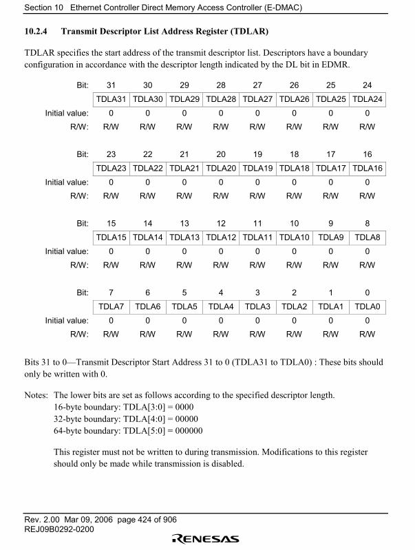
Section 10 Ethernet Controller Direct Memory Access Controller (E-DMAC)
Rev. 2.00 Mar 09, 2006 page 424 of 906REJ09B0292-0200
10.2.4 Transmit Descriptor List Address Register (TDLAR)
TDLAR specifies the start address of the transmit descriptor list. Descriptors have a boundaryconfiguration in accordance with the descriptor length indicated by the DL bit in EDMR.
Bit: 31 30 29 28 27 26 25 24
TDLA31 TDLA30 TDLA29 TDLA28 TDLA27 TDLA26 TDLA25 TDLA24
Initial value: 0 0 0 0 0 0 0 0
R/W: R/W R/W R/W R/W R/W R/W R/W R/W
Bit: 23 22 21 20 19 18 17 16
TDLA23 TDLA22 TDLA21 TDLA20 TDLA19 TDLA18 TDLA17 TDLA16
Initial value: 0 0 0 0 0 0 0 0
R/W: R/W R/W R/W R/W R/W R/W R/W R/W
Bit: 15 14 13 12 11 10 9 8
TDLA15 TDLA14 TDLA13 TDLA12 TDLA11 TDLA10 TDLA9 TDLA8
Initial value: 0 0 0 0 0 0 0 0
R/W: R/W R/W R/W R/W R/W R/W R/W R/W
Bit: 7 6 5 4 3 2 1 0
TDLA7 TDLA6 TDLA5 TDLA4 TDLA3 TDLA2 TDLA1 TDLA0
Initial value: 0 0 0 0 0 0 0 0
R/W: R/W R/W R/W R/W R/W R/W R/W R/W
Bits 31 to 0�Transmit Descriptor Start Address 31 to 0 (TDLA31 to TDLA0) : These bits shouldonly be written with 0.
Notes: The lower bits are set as follows according to the specified descriptor length.16-byte boundary: TDLA[3:0] = 000032-byte boundary: TDLA[4:0] = 0000064-byte boundary: TDLA[5:0] = 000000
This register must not be written to during transmission. Modifications to this registershould only be made while transmission is disabled.
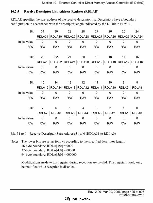
Section 10 Ethernet Controller Direct Memory Access Controller (E-DMAC)
Rev. 2.00 Mar 09, 2006 page 425 of 906REJ09B0292-0200
10.2.5 Receive Descriptor List Address Register (RDLAR)
RDLAR specifies the start address of the receive descriptor list. Descriptors have a boundaryconfiguration in accordance with the descriptor length indicated by the DL bit in EDMR.
Bit: 31 30 29 28 27 26 25 24
RDLA31 RDLA30 RDLA29 RDLA28 RDLA27 RDLA26 RDLA25 RDLA24
Initial value: 0 0 0 0 0 0 0 0
R/W: R/W R/W R/W R/W R/W R/W R/W R/W
Bit: 23 22 21 20 19 18 17 16
RDLA23 RDLA22 RDLA21 RDLA20 RDLA19 RDLA18 RDLA17 RDLA16
Initial value: 0 0 0 0 0 0 0 0
R/W: R/W R/W R/W R/W R/W R/W R/W R/W
Bit: 15 14 13 12 11 10 9 8
RDLA15 RDLA14 RDLA13 RDLA12 RDLA11 RDLA10 RDLA9 RDLA8
Initial value: 0 0 0 0 0 0 0 0
R/W: R/W R/W R/W R/W R/W R/W R/W R/W
Bit: 7 6 5 4 3 2 1 0
RDLA7 RDLA6 RDLA5 RDLA4 RDLA3 RDLA2 RDLA1 RDLA0
Initial value: 0 0 0 0 0 0 0 0
R/W: R/W R/W R/W R/W R/W R/W R/W R/W
Bits 31 to 0�Receive Descriptor Start Address 31 to 0 (RDLA31 to RDLA0)
Notes: The lower bits are set as follows according to the specified descriptor length.16-byte boundary: RDLA[3:0] = 000032-byte boundary: RDLA[4:0] = 0000064-byte boundary: RDLA[5:0] = 000000
Modifications made to this register during reception are invalid. This register should onlybe modified while reception is disabled.
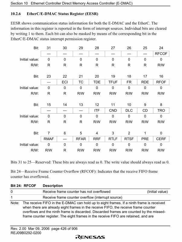
Section 10 Ethernet Controller Direct Memory Access Controller (E-DMAC)
Rev. 2.00 Mar 09, 2006 page 426 of 906REJ09B0292-0200
10.2.6 EtherC/E-DMAC Status Register (EESR)
EESR shows communication status information for both the E-DMAC and the EtherC. Theinformation in this register is reported in the form of interrupt sources. Individual bits are clearedby writing 1 to them. Each bit can also be masked by means of the corresponding bit in theEtherC/E-DMAC status interrupt permission register.
Bit: 31 30 29 28 27 26 25 24� � � � � � � RFCOF
Initial value: 0 0 0 0 0 0 0 0R/W: R R R R R R R R/W
Bit: 23 22 21 20 19 18 17 16� ECI TC TDE TFUF FR RDE RFOF
Initial value: 0 0 0 0 0 0 0 0R/W: R R R/W R/W R/W R/W R/W R/W
Bit: 15 14 13 12 11 10 9 8� � � ITF CND DLC CD TRO
Initial value: 0 0 0 0 0 0 0 0R/W: R R R R/W R/W R/W R/W R/W
Bit: 7 6 5 4 3 2 1 0RMAF � RFAR RRF RTLF RTSF PRE CERF
Initial value: 0 0 0 0 0 0 0 0R/W: R/W R R/W R/W R/W R/W R/W R/W
Bits 31 to 25�Reserved: These bits are always read as 0. The write value should always read as 0.
Bit 24�Receive Frame Counter Overflow (RFCOF): Indicates that the receive FIFO framecounter has overflowed.
Bit 24: RFCOF Description0 Receive frame counter has not overflowed (Initial value)1 Receive frame counter overflow (interrupt source)Note: The receive FIFO in the E-DMAC can hold up to eight frames. If a ninth frame is received
when there are already eight frames in the receive FIFO, the receive frame counteroverflows and the ninth frame is discarded. Discarded frames are counted by the missed-frame counter register. The eight frames in the receive FIFO are retained, and are
Section 10 Ethernet Controller Direct Memory Access Controller (E-DMAC)
Rev. 2.00 Mar 09, 2006 page 427 of 906REJ09B0292-0200
transferred to memory when DMA transfer becomes possible. When the frame countervalue falls below 8, another frame is received.
Bit 23�Reserved: These bits are always read as 0. The write value should always be 0.
Bit 22�EtherC States Register Interrupt (ECI): Indicates that an interrupt due to an EtherC statusregister (ECSR) source has been detected.
Bit 22: ECI Description
0 EtherC status interrupt source not detected (Initial value)
1 EtherC status interrupt source detected (interrupt source)Note: EESR is a read-only register. When this register is cleared by a source in ECSR in the
EtherC, this bit is also cleared.
Bit 21�Frame Transmit Complete (TC): Indicates that all the data specified by the transmitdescriptor has been transmitted to the EtherC. The transfer status is written back to the relevantdescriptor. When 1-frame transmission is completed for 1-frame/1-buffer processing, or when thelast data in the frame is transmitted and the transmission descriptor valid bit (TACT) in the nextdescriptor is not set for multiple-frame buffer processing, transmission is completed and this bit isset to 1. After frame transmission, the E-DMAC writes the transmission status back to thedescriptor.
Bit 21: TC Description
0 Transfer not complete, or no transfer directive (Initial value)
1 Transfer complete (interrupt source)Note: As data is sent onto the line by the PHY-LSI from the EtherC via the MII, the actual
transmission completion time is longer.
Bit 20�Transmit Descriptor Exhausted (TDE): Indicates that the transmission descriptor valid bit(TACT) in the descriptor is not set when the E-DMAC reads the transmission descriptor when theprevious descriptor is not the last one of the frame for multiple- buffer frame processing. As aresult, an incomplete frame may be transmitted.
Bit 20: TDE Description
0 �1� transmit descriptor active bit (TACT) detected (Initial value)
1 �0� transmit descriptor active bit (TACT) detected (interrupt source)Note: When transmission descriptor empty (TDE = 1) occurs, execute a software reset and initiate
transmission. In this case, the address that is stored in the transmit descriptor list addressregister (TDLAR) is transmitted first.

Section 10 Ethernet Controller Direct Memory Access Controller (E-DMAC)
Rev. 2.00 Mar 09, 2006 page 428 of 906REJ09B0292-0200
Bit 19�Transmit FIFO Underflow (TFUF): Indicates that underflow has occurred in the transmitFIFO during frame transmission. Incomplete data is sent onto the line.
Bit 19: TFUF Description
0 Underflow has not occurred (Initial value)
1 Underflow has occurred (interrupt source)Note: Whether E-DMAC operation continues or halts after underflow is controlled by the E-DMAC
operation control register (EDOCR).
Bit 18�Frame Received (FR): Indicates that a frame has been received and the receive descriptorhas been updated. This bit is set to 1 each time a frame is received.
Note: The actual receive frame status is indicated in the receive status field in the descriptor.
Bit 18: FR Description
0 Frame not received (Initial value)
1 Frame received (interrupt source)
Bit 17�Receive Descriptor Exhausted (RDE): This bit is set if the receive descriptor active bit(RACT) setting is �inactive� (RACT = 0) when the E-DMAC reads a receive descriptor.
Bit 17: RDE Description
0 �1� receive descriptor active bit (RACT) detected (Initial value)
1 �0� receive descriptor active bit (RACT) detected (interrupt source)Note: When receive descriptor empty (RDE = 1) occurs, receiving can be restarted by setting
RACT = 1 in the receive descriptor and initiating receiving.
Bit 16�Receive FIFO Overflow (RFOF): Indicates that the receive FIFO has overflowed duringframe reception.
Bit 16: RFOF Description
0 Overflow has not occurred (Initial value)
1 Overflow has occurred (interrupt source)Notes: 1. If there are a number of receive frames in the receive FIFO, they will not be sent to
memory correctly. The status of the frame that caused the overflow is written back tothe receive descriptor.
2. Whether E-DMAC operation continues or halts after overflow is controlled by the E-DMAC operation control register (EDOCR).
Section 10 Ethernet Controller Direct Memory Access Controller (E-DMAC)
Rev. 2.00 Mar 09, 2006 page 429 of 906REJ09B0292-0200
Bits 15 to 13�Reserved: These bits are always read as 0. The write value should always be 0.
Bit 12�Illegal Transmit Frame (ITF): Indicates that the transmit frame length specification is lessthan four bytes.
Bit 12: ITF Description
0 Normal transmit frame length (Initial value)
1 Illegal transmit frame length (interrupt source)
Bit 11�Carrier Not Detect (CND): Indicates the carrier detection status.
Bit 11: CND Description
0 A carrier is detected when transmission starts (Initial value)
1 Carrier not detected (interrupt source)
Bit 10�Detect Loss of Carrier (DLC): Indicates that loss of the carrier has been detected duringframe transmission.
Bit 10: DLC Description
0 Loss of carrier not detected (Initial value)
1 Loss of carrier detected (interrupt source)
Bit 9�Collision Detect (CD): Indicates that a collision has been detected during frametransmission.
Bit 9: CD Description
0 Collision not detected (Initial value)
1 Collision detected (interrupt source)
Bit 8�Transmit Retry Over (TRO): Indicates that a retry-over condition has occurred duringframe transmission. Total 16 transmission retries including 15 retries based on the back-offalgorithm are failed after the EtherC transmission starts.
Bit 8: TRO Description
0 Transmit retry-over condition not detected (Initial value)
1 Transmit retry-over condition detected (interrupt source)
Section 10 Ethernet Controller Direct Memory Access Controller (E-DMAC)
Rev. 2.00 Mar 09, 2006 page 430 of 906REJ09B0292-0200
Bit 7�Receive Multicast Address Frame (RMAF): Indicates that a multicast address frame hasbeen received.
Bit 7: RMAF Description
0 Multicast address frame has not been received (Initial value)
1 Multicast address frame has been received (interrupt source)
Bits 6�Reserved: This bit should only be written with 0.
Bit 5��Receive Frame Discard Request Assertion (RFAR): Indicates that a frame discard requesthas been asserted by the EtherC as a result of a signal from the CAM, however, it is not possible todiscard the frame in the E-DMAC.
Bit 5: RFAR Description
0 Receive frame discard request assertion has not been received (Initial value)
1 Receive frame discard request assertion has been received (interrupt source)
Bit 4�Receive Residual-Bit Frame (RRF): Indicates that a residual-bit frame has been received.
Bit 4: RRF Description
0 Residual-bit frame has not been received (Initial value)
1 Residual-bit frame has been received (interrupt source)
Bit 3�Receive Too-Long Frame (RTLF): Indicates that a frame of 1519 bytes or longer has beenreceived.
Bit 3: RTLF Description
0 Too-long frame has not been received (Initial value)
1 Too-long frame has been received (interrupt source)
Bit 2�Receive Too-Short Frame (RTSF): Indicates that a frame of fewer than 64 bytes has beenreceived.
Bit 2: RTSF Description
0 Too-short frame has not been received (Initial value)
1 Too-short frame has been received (interrupt source)
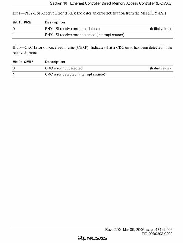
Section 10 Ethernet Controller Direct Memory Access Controller (E-DMAC)
Rev. 2.00 Mar 09, 2006 page 431 of 906REJ09B0292-0200
Bit 1�PHY-LSI Receive Error (PRE): Indicates an error notification from the MII (PHY-LSI)
Bit 1: PRE Description
0 PHY-LSI receive error not detected (Initial value)
1 PHY-LSI receive error detected (interrupt source)
Bit 0�CRC Error on Received Frame (CERF): Indicates that a CRC error has been detected in thereceived frame.
Bit 0: CERF Description
0 CRC error not detected (Initial value)
1 CRC error detected (interrupt source)
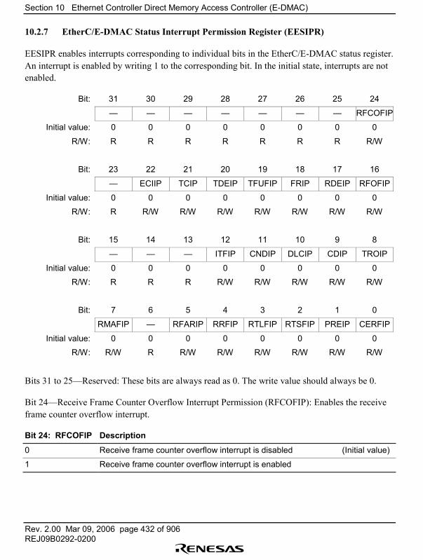
Section 10 Ethernet Controller Direct Memory Access Controller (E-DMAC)
Rev. 2.00 Mar 09, 2006 page 432 of 906REJ09B0292-0200
10.2.7 EtherC/E-DMAC Status Interrupt Permission Register (EESIPR)
EESIPR enables interrupts corresponding to individual bits in the EtherC/E-DMAC status register.An interrupt is enabled by writing 1 to the corresponding bit. In the initial state, interrupts are notenabled.
Bit: 31 30 29 28 27 26 25 24
� � � � � � � RFCOFIP
Initial value: 0 0 0 0 0 0 0 0
R/W: R R R R R R R R/W
Bit: 23 22 21 20 19 18 17 16
� ECIIP TCIP TDEIP TFUFIP FRIP RDEIP RFOFIP
Initial value: 0 0 0 0 0 0 0 0
R/W: R R/W R/W R/W R/W R/W R/W R/W
Bit: 15 14 13 12 11 10 9 8
� � � ITFIP CNDIP DLCIP CDIP TROIP
Initial value: 0 0 0 0 0 0 0 0
R/W: R R R R/W R/W R/W R/W R/W
Bit: 7 6 5 4 3 2 1 0
RMAFIP � RFARIP RRFIP RTLFIP RTSFIP PREIP CERFIP
Initial value: 0 0 0 0 0 0 0 0
R/W: R/W R R/W R/W R/W R/W R/W R/W
Bits 31 to 25�Reserved: These bits are always read as 0. The write value should always be 0.
Bit 24�Receive Frame Counter Overflow Interrupt Permission (RFCOFIP): Enables the receiveframe counter overflow interrupt.
Bit 24: RFCOFIP Description
0 Receive frame counter overflow interrupt is disabled (Initial value)
1 Receive frame counter overflow interrupt is enabled
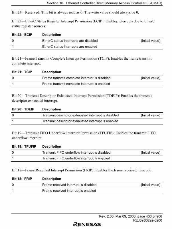
Section 10 Ethernet Controller Direct Memory Access Controller (E-DMAC)
Rev. 2.00 Mar 09, 2006 page 433 of 906REJ09B0292-0200
Bit 23�Reserved: This bit is always read as 0. The write value should always be 0.
Bit 22�EtherC Status Register Interrupt Permission (ECIP): Enables interrupts due to EtherCstatus register sources.
Bit 22: ECIP Description
0 EtherC status interrupts are disabled (Initial value)
1 EtherC status interrupts are enabled
Bit 21�Frame Transmit Complete Interrupt Permission (TCIP): Enables the frame transmitcomplete interrupt.
Bit 21: TCIP Description
0 Frame transmit complete interrupt is disabled (Initial value)
1 Frame transmit complete interrupt is enabled
Bit 20�Transmit Descriptor Exhausted Interrupt Permission (TDEIP): Enables the transmitdescriptor exhausted interrupt.
Bit 20: TDEIP Description
0 Transmit descriptor exhausted interrupt is disabled (Initial value)
1 Transmit descriptor exhausted interrupt is enabled
Bit 19�Transmit FIFO Underflow Interrupt Permission (TFUFIP): Enables the transmit FIFOunderflow interrupt.
Bit 19: TFUFIP Description
0 Transmit FIFO underflow interrupt is disabled (Initial value)
1 Transmit FIFO underflow interrupt is enabled
Bit 18�Frame Received Interrupt Permission (FRIP): Enables the frame received interrupt.
Bit 18: FRIP Description
0 Frame received interrupt is disabled (Initial value)
1 Frame received interrupt is enabled
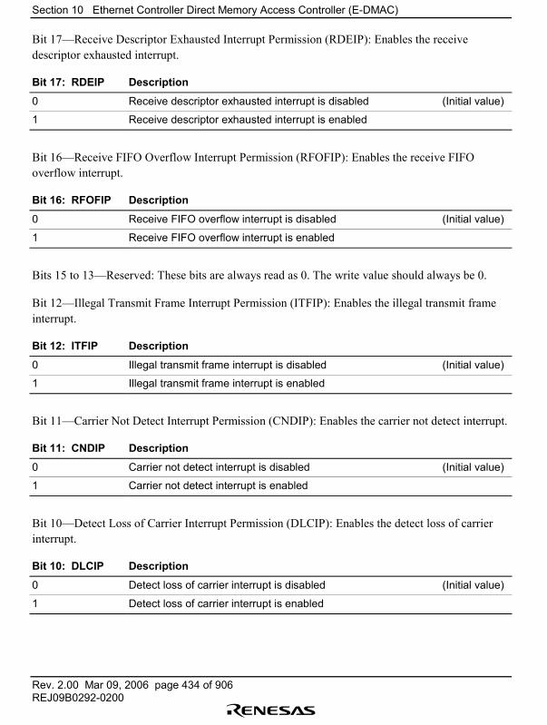
Section 10 Ethernet Controller Direct Memory Access Controller (E-DMAC)
Rev. 2.00 Mar 09, 2006 page 434 of 906REJ09B0292-0200
Bit 17�Receive Descriptor Exhausted Interrupt Permission (RDEIP): Enables the receivedescriptor exhausted interrupt.
Bit 17: RDEIP Description
0 Receive descriptor exhausted interrupt is disabled (Initial value)
1 Receive descriptor exhausted interrupt is enabled
Bit 16�Receive FIFO Overflow Interrupt Permission (RFOFIP): Enables the receive FIFOoverflow interrupt.
Bit 16: RFOFIP Description
0 Receive FIFO overflow interrupt is disabled (Initial value)
1 Receive FIFO overflow interrupt is enabled
Bits 15 to 13�Reserved: These bits are always read as 0. The write value should always be 0.
Bit 12�Illegal Transmit Frame Interrupt Permission (ITFIP): Enables the illegal transmit frameinterrupt.
Bit 12: ITFIP Description
0 Illegal transmit frame interrupt is disabled (Initial value)
1 Illegal transmit frame interrupt is enabled
Bit 11�Carrier Not Detect Interrupt Permission (CNDIP): Enables the carrier not detect interrupt.
Bit 11: CNDIP Description
0 Carrier not detect interrupt is disabled (Initial value)
1 Carrier not detect interrupt is enabled
Bit 10�Detect Loss of Carrier Interrupt Permission (DLCIP): Enables the detect loss of carrierinterrupt.
Bit 10: DLCIP Description
0 Detect loss of carrier interrupt is disabled (Initial value)
1 Detect loss of carrier interrupt is enabled
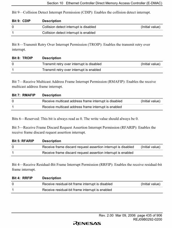
Section 10 Ethernet Controller Direct Memory Access Controller (E-DMAC)
Rev. 2.00 Mar 09, 2006 page 435 of 906REJ09B0292-0200
Bit 9�Collision Detect Interrupt Permission (CDIP): Enables the collision detect interrupt.
Bit 9: CDIP Description
0 Collision detect interrupt is disabled (Initial value)
1 Collision detect interrupt is enabled
Bit 8�Transmit Retry Over Interrupt Permission (TROIP): Enables the transmit retry overinterrupt.
Bit 8: TROIP Description
0 Transmit retry over interrupt is disabled (Initial value)
1 Transmit retry over interrupt is enabled
Bit 7�Receive Multicast Address Frame Interrupt Permission (RMAFIP): Enables the receivemulticast address frame interrupt.
Bit 7: RMAFIP Description
0 Receive multicast address frame interrupt is disabled (Initial value)
1 Receive multicast address frame interrupt is enabled
Bits 6�Reserved: This bit is always read as 0. The write value should always be 0.
Bit 5��Receive Frame Discard Request Assertion Interrupt Permission (RFARIP): Enables thereceive frame discard request assertion interrupt.
Bit 5: RFARIP Description
0 Receive frame discard request assertion interrupt is disabled (Initial value)
1 Receive frame discard request assertion interrupt is enabled
Bit 4�Receive Residual-Bit Frame Interrupt Permission (RRFIP): Enables the receive residual-bitframe interrupt.
Bit 4: RRFIP Description
0 Receive residual-bit frame interrupt is disabled (Initial value)
1 Receive residual-bit frame interrupt is enabled
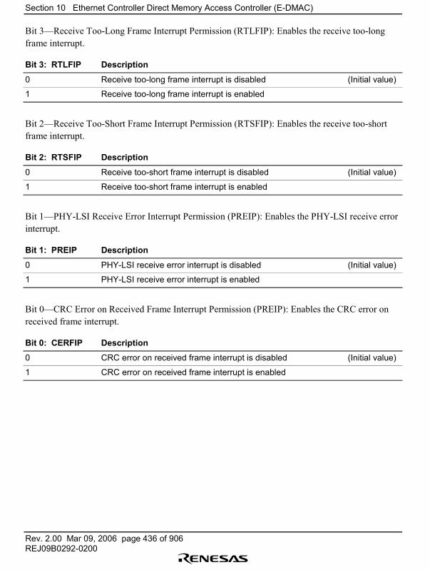
Section 10 Ethernet Controller Direct Memory Access Controller (E-DMAC)
Rev. 2.00 Mar 09, 2006 page 436 of 906REJ09B0292-0200
Bit 3�Receive Too-Long Frame Interrupt Permission (RTLFIP): Enables the receive too-longframe interrupt.
Bit 3: RTLFIP Description
0 Receive too-long frame interrupt is disabled (Initial value)
1 Receive too-long frame interrupt is enabled
Bit 2�Receive Too-Short Frame Interrupt Permission (RTSFIP): Enables the receive too-shortframe interrupt.
Bit 2: RTSFIP Description
0 Receive too-short frame interrupt is disabled (Initial value)
1 Receive too-short frame interrupt is enabled
Bit 1�PHY-LSI Receive Error Interrupt Permission (PREIP): Enables the PHY-LSI receive errorinterrupt.
Bit 1: PREIP Description
0 PHY-LSI receive error interrupt is disabled (Initial value)
1 PHY-LSI receive error interrupt is enabled
Bit 0�CRC Error on Received Frame Interrupt Permission (PREIP): Enables the CRC error onreceived frame interrupt.
Bit 0: CERFIP Description
0 CRC error on received frame interrupt is disabled (Initial value)
1 CRC error on received frame interrupt is enabled
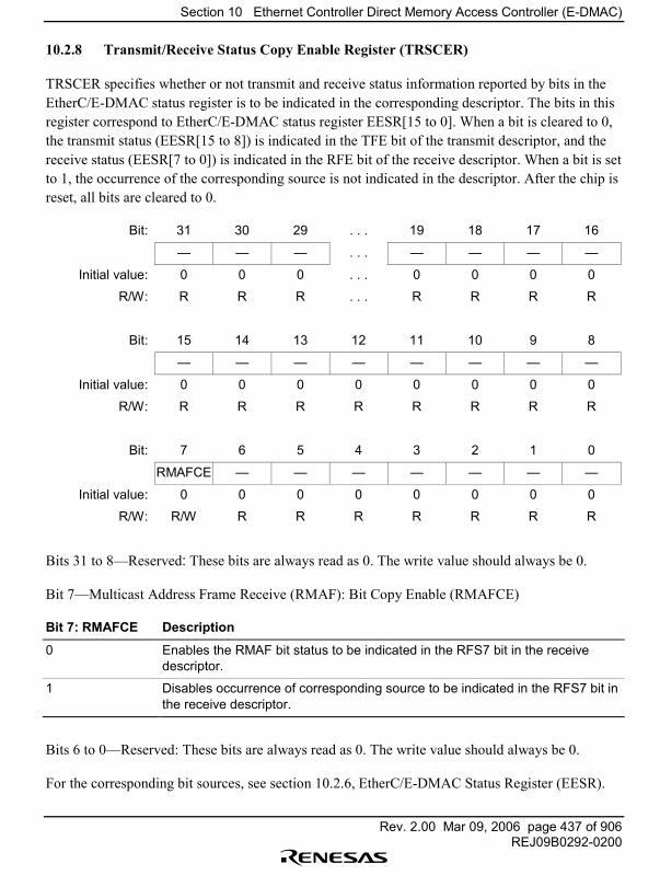
Section 10 Ethernet Controller Direct Memory Access Controller (E-DMAC)
Rev. 2.00 Mar 09, 2006 page 437 of 906REJ09B0292-0200
10.2.8 Transmit/Receive Status Copy Enable Register (TRSCER)
TRSCER specifies whether or not transmit and receive status information reported by bits in theEtherC/E-DMAC status register is to be indicated in the corresponding descriptor. The bits in thisregister correspond to EtherC/E-DMAC status register EESR[15 to 0]. When a bit is cleared to 0,the transmit status (EESR[15 to 8]) is indicated in the TFE bit of the transmit descriptor, and thereceive status (EESR[7 to 0]) is indicated in the RFE bit of the receive descriptor. When a bit is setto 1, the occurrence of the corresponding source is not indicated in the descriptor. After the chip isreset, all bits are cleared to 0.
Bit: 31 30 29 . . . 19 18 17 16
� � � . . . � � � �
Initial value: 0 0 0 . . . 0 0 0 0
R/W: R R R . . . R R R R
Bit: 15 14 13 12 11 10 9 8
� � � � � � � �
Initial value: 0 0 0 0 0 0 0 0
R/W: R R R R R R R R
Bit: 7 6 5 4 3 2 1 0
RMAFCE � � � � � � �
Initial value: 0 0 0 0 0 0 0 0
R/W: R/W R R R R R R R
Bits 31 to 8�Reserved: These bits are always read as 0. The write value should always be 0.
Bit 7�Multicast Address Frame Receive (RMAF): Bit Copy Enable (RMAFCE)
Bit 7: RMAFCE Description
0 Enables the RMAF bit status to be indicated in the RFS7 bit in the receivedescriptor.
1 Disables occurrence of corresponding source to be indicated in the RFS7 bit inthe receive descriptor.
Bits 6 to 0�Reserved: These bits are always read as 0. The write value should always be 0.
For the corresponding bit sources, see section 10.2.6, EtherC/E-DMAC Status Register (EESR).
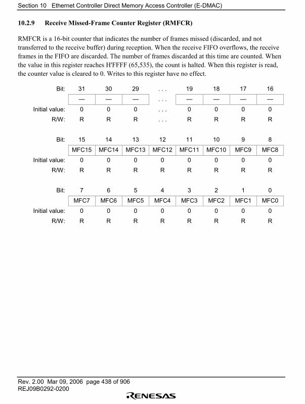
Section 10 Ethernet Controller Direct Memory Access Controller (E-DMAC)
Rev. 2.00 Mar 09, 2006 page 438 of 906REJ09B0292-0200
10.2.9 Receive Missed-Frame Counter Register (RMFCR)
RMFCR is a 16-bit counter that indicates the number of frames missed (discarded, and nottransferred to the receive buffer) during reception. When the receive FIFO overflows, the receiveframes in the FIFO are discarded. The number of frames discarded at this time are counted. Whenthe value in this register reaches H'FFFF (65,535), the count is halted. When this register is read,the counter value is cleared to 0. Writes to this register have no effect.
Bit: 31 30 29 . . . 19 18 17 16
� � � . . . � � � �
Initial value: 0 0 0 . . . 0 0 0 0
R/W: R R R . . . R R R R
Bit: 15 14 13 12 11 10 9 8
MFC15 MFC14 MFC13 MFC12 MFC11 MFC10 MFC9 MFC8
Initial value: 0 0 0 0 0 0 0 0
R/W: R R R R R R R R
Bit: 7 6 5 4 3 2 1 0
MFC7 MFC6 MFC5 MFC4 MFC3 MFC2 MFC1 MFC0
Initial value: 0 0 0 0 0 0 0 0
R/W: R R R R R R R R
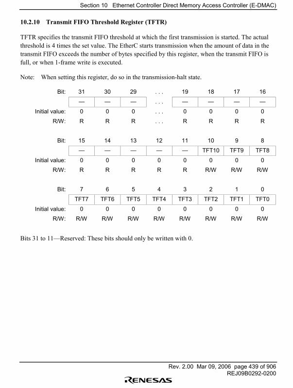
Section 10 Ethernet Controller Direct Memory Access Controller (E-DMAC)
Rev. 2.00 Mar 09, 2006 page 439 of 906REJ09B0292-0200
10.2.10 Transmit FIFO Threshold Register (TFTR)
TFTR specifies the transmit FIFO threshold at which the first transmission is started. The actualthreshold is 4 times the set value. The EtherC starts transmission when the amount of data in thetransmit FIFO exceeds the number of bytes specified by this register, when the transmit FIFO isfull, or when 1-frame write is executed.
Note: When setting this register, do so in the transmission-halt state.
Bit: 31 30 29 . . . 19 18 17 16
� � � . . . � � � �
Initial value: 0 0 0 . . . 0 0 0 0
R/W: R R R . . . R R R R
Bit: 15 14 13 12 11 10 9 8
� � � � � TFT10 TFT9 TFT8
Initial value: 0 0 0 0 0 0 0 0
R/W: R R R R R R/W R/W R/W
Bit: 7 6 5 4 3 2 1 0
TFT7 TFT6 TFT5 TFT4 TFT3 TFT2 TFT1 TFT0
Initial value: 0 0 0 0 0 0 0 0
R/W: R/W R/W R/W R/W R/W R/W R/W R/W
Bits 31 to 11�Reserved: These bits should only be written with 0.
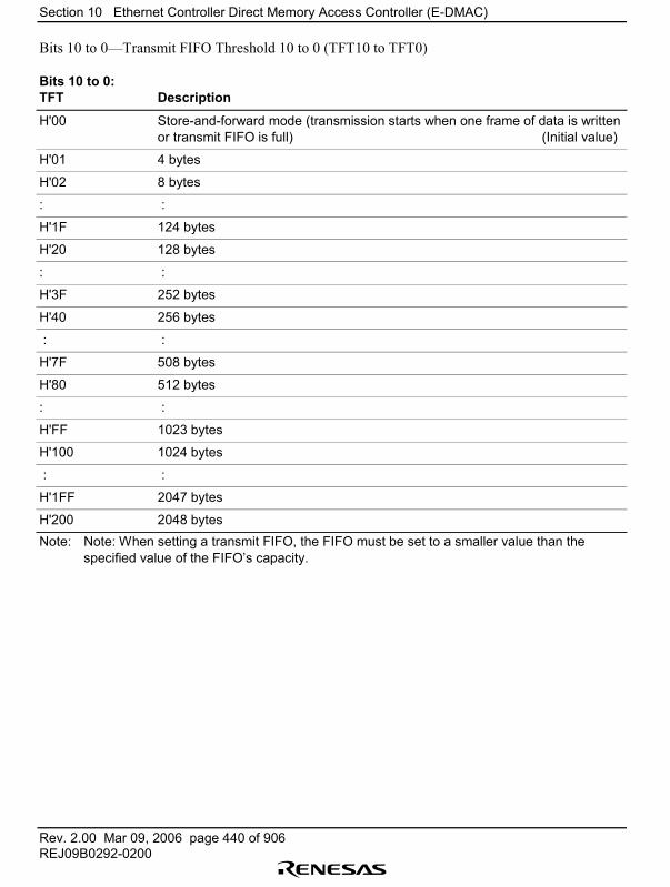
Section 10 Ethernet Controller Direct Memory Access Controller (E-DMAC)
Rev. 2.00 Mar 09, 2006 page 440 of 906REJ09B0292-0200
Bits 10 to 0�Transmit FIFO Threshold 10 to 0 (TFT10 to TFT0)
Bits 10 to 0:TFT Description
H'00 Store-and-forward mode (transmission starts when one frame of data is writtenor transmit FIFO is full) (Initial value)
H'01 4 bytes
H'02 8 bytes
: :
H'1F 124 bytes
H'20 128 bytes
: :
H'3F 252 bytes
H'40 256 bytes
: :
H'7F 508 bytes
H'80 512 bytes
: :
H'FF 1023 bytes
H'100 1024 bytes
: :
H'1FF 2047 bytes
H'200 2048 bytesNote: Note: When setting a transmit FIFO, the FIFO must be set to a smaller value than the
specified value of the FIFO�s capacity.
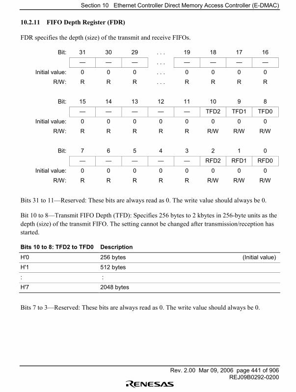
Section 10 Ethernet Controller Direct Memory Access Controller (E-DMAC)
Rev. 2.00 Mar 09, 2006 page 441 of 906REJ09B0292-0200
10.2.11 FIFO Depth Register (FDR)
FDR specifies the depth (size) of the transmit and receive FIFOs.
Bit: 31 30 29 . . . 19 18 17 16
� � � . . . � � � �
Initial value: 0 0 0 . . . 0 0 0 0
R/W: R R R . . . R R R R
Bit: 15 14 13 12 11 10 9 8
� � � � � TFD2 TFD1 TFD0
Initial value: 0 0 0 0 0 0 0 0
R/W: R R R R R R/W R/W R/W
Bit: 7 6 5 4 3 2 1 0
� � � � � RFD2 RFD1 RFD0
Initial value: 0 0 0 0 0 0 0 0
R/W: R R R R R R/W R/W R/W
Bits 31 to 11�Reserved: These bits are always read as 0. The write value should always be 0.
Bit 10 to 8�Transmit FIFO Depth (TFD): Specifies 256 bytes to 2 kbytes in 256-byte units as thedepth (size) of the transmit FIFO. The setting cannot be changed after transmission/reception hasstarted.
Bits 10 to 8: TFD2 to TFD0 Description
H'0 256 bytes (Initial value)
H'1 512 bytes
: :
H'7 2048 bytes
Bits 7 to 3�Reserved: These bits are always read as 0. The write value should always be 0.
Section 10 Ethernet Controller Direct Memory Access Controller (E-DMAC)
Rev. 2.00 Mar 09, 2006 page 442 of 906REJ09B0292-0200
Bit 2 to 0�Receive FIFO Depth (RFD): Specifies 256 bytes to 2 kbytes in 256-byte units as thedepth (size) of the receive FIFO. The actual FIFO depth is 256 times the set value. The settingcannot be changed after transmission/reception has started.
Bits 2 to 0: RFD2 to RFD0 Description
H'0 256 bytes (Initial value)
H'1 512 bytes
: :
H'7 2048 bytes
10.2.12 Receiver Control Register (RCR)
RCR specifies the control method for the RE bit in ECMR when a frame is received.
Note: When setting this register, do so in the receiving-halt state.
Bit: 31 30 29 . . . 11 10 9 8
� � � . . . � � � �
Initial value: 0 0 0 . . . 0 0 0 0
R/W: R R R . . . R R R R
Bit: 7 6 5 4 3 2 1 0
� � � � � � � RNC
Initial value: 0 0 0 0 0 0 0 0
R/W: R R R R R R R R/W
Bits 31 to 1�Reserved: These bits are always read as 0. The write value should always be 0.
Bit 0�Receive Enable Control (RNC)
Bit 0: RNC Description
0 When reception of one frame is completed, the E-DMAC writes the receivestatus into the descriptor and clears the RR bit in EDRRR (Initial value)
1 When reception of one frame is completed, the E-DMAC writes the receivestatus into the descriptor, reads the next descriptor, and prepares to receivethe next frame*
Note: * This setting is normally used for continuous frame reception.
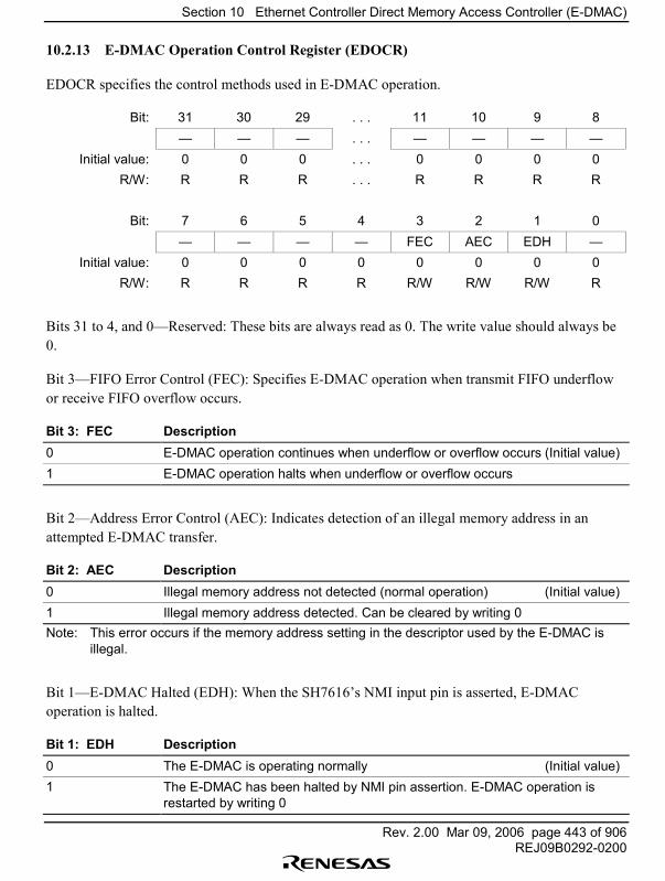
Section 10 Ethernet Controller Direct Memory Access Controller (E-DMAC)
Rev. 2.00 Mar 09, 2006 page 443 of 906REJ09B0292-0200
10.2.13 E-DMAC Operation Control Register (EDOCR)
EDOCR specifies the control methods used in E-DMAC operation.
Bit: 31 30 29 . . . 11 10 9 8� � � . . . � � � �
Initial value: 0 0 0 . . . 0 0 0 0R/W: R R R . . . R R R R
Bit: 7 6 5 4 3 2 1 0� � � � FEC AEC EDH �
Initial value: 0 0 0 0 0 0 0 0R/W: R R R R R/W R/W R/W R
Bits 31 to 4, and 0�Reserved: These bits are always read as 0. The write value should always be0.
Bit 3�FIFO Error Control (FEC): Specifies E-DMAC operation when transmit FIFO underflowor receive FIFO overflow occurs.
Bit 3: FEC Description0 E-DMAC operation continues when underflow or overflow occurs (Initial value)1 E-DMAC operation halts when underflow or overflow occurs
Bit 2�Address Error Control (AEC): Indicates detection of an illegal memory address in anattempted E-DMAC transfer.
Bit 2: AEC Description0 Illegal memory address not detected (normal operation) (Initial value)1 Illegal memory address detected. Can be cleared by writing 0Note: This error occurs if the memory address setting in the descriptor used by the E-DMAC is
illegal.
Bit 1�E-DMAC Halted (EDH): When the SH7616�s NMI input pin is asserted, E-DMACoperation is halted.
Bit 1: EDH Description0 The E-DMAC is operating normally (Initial value)1 The E-DMAC has been halted by NMI pin assertion. E-DMAC operation is
restarted by writing 0
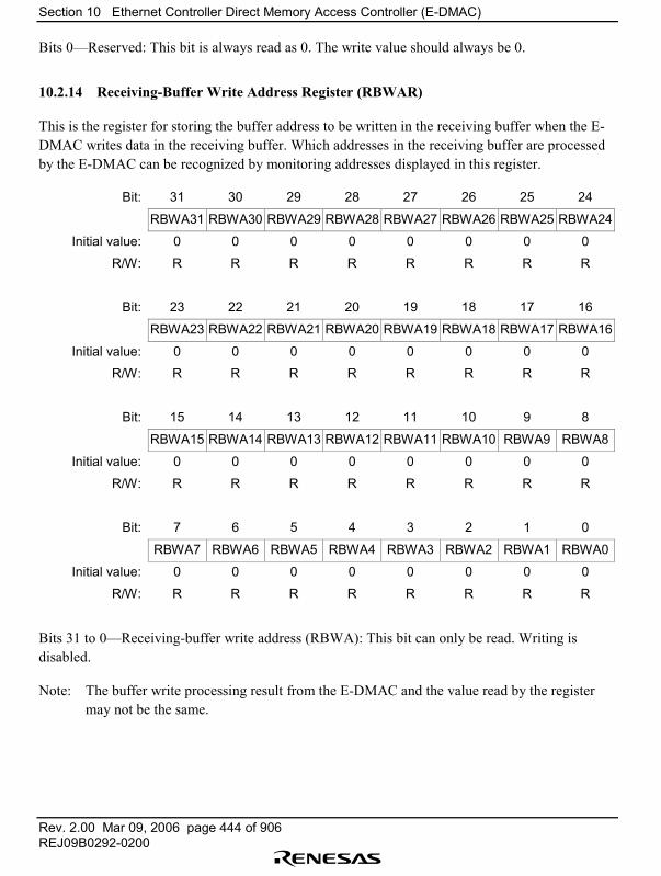
Section 10 Ethernet Controller Direct Memory Access Controller (E-DMAC)
Rev. 2.00 Mar 09, 2006 page 444 of 906REJ09B0292-0200
Bits 0�Reserved: This bit is always read as 0. The write value should always be 0.
10.2.14 Receiving-Buffer Write Address Register (RBWAR)
This is the register for storing the buffer address to be written in the receiving buffer when the E-DMAC writes data in the receiving buffer. Which addresses in the receiving buffer are processedby the E-DMAC can be recognized by monitoring addresses displayed in this register.
Bit: 31 30 29 28 27 26 25 24
RBWA31 RBWA30 RBWA29 RBWA28 RBWA27 RBWA26 RBWA25 RBWA24
Initial value: 0 0 0 0 0 0 0 0
R/W: R R R R R R R R
Bit: 23 22 21 20 19 18 17 16
RBWA23 RBWA22 RBWA21 RBWA20 RBWA19 RBWA18 RBWA17 RBWA16
Initial value: 0 0 0 0 0 0 0 0
R/W: R R R R R R R R
Bit: 15 14 13 12 11 10 9 8
RBWA15 RBWA14 RBWA13 RBWA12 RBWA11 RBWA10 RBWA9 RBWA8
Initial value: 0 0 0 0 0 0 0 0
R/W: R R R R R R R R
Bit: 7 6 5 4 3 2 1 0
RBWA7 RBWA6 RBWA5 RBWA4 RBWA3 RBWA2 RBWA1 RBWA0
Initial value: 0 0 0 0 0 0 0 0
R/W: R R R R R R R R
Bits 31 to 0�Receiving-buffer write address (RBWA): This bit can only be read. Writing isdisabled.
Note: The buffer write processing result from the E-DMAC and the value read by the registermay not be the same.
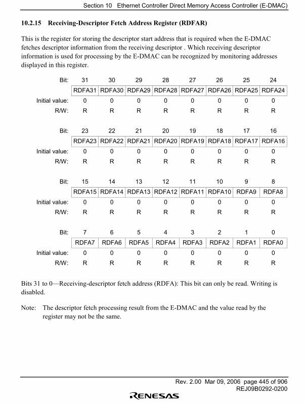
Section 10 Ethernet Controller Direct Memory Access Controller (E-DMAC)
Rev. 2.00 Mar 09, 2006 page 445 of 906REJ09B0292-0200
10.2.15 Receiving-Descriptor Fetch Address Register (RDFAR)
This is the register for storing the descriptor start address that is required when the E-DMACfetches descriptor information from the receiving descriptor . Which receiving descriptorinformation is used for processing by the E-DMAC can be recognized by monitoring addressesdisplayed in this register.
Bit: 31 30 29 28 27 26 25 24
RDFA31 RDFA30 RDFA29 RDFA28 RDFA27 RDFA26 RDFA25 RDFA24
Initial value: 0 0 0 0 0 0 0 0
R/W: R R R R R R R R
Bit: 23 22 21 20 19 18 17 16
RDFA23 RDFA22 RDFA21 RDFA20 RDFA19 RDFA18 RDFA17 RDFA16
Initial value: 0 0 0 0 0 0 0 0
R/W: R R R R R R R R
Bit: 15 14 13 12 11 10 9 8
RDFA15 RDFA14 RDFA13 RDFA12 RDFA11 RDFA10 RDFA9 RDFA8
Initial value: 0 0 0 0 0 0 0 0
R/W: R R R R R R R R
Bit: 7 6 5 4 3 2 1 0
RDFA7 RDFA6 RDFA5 RDFA4 RDFA3 RDFA2 RDFA1 RDFA0
Initial value: 0 0 0 0 0 0 0 0
R/W: R R R R R R R R
Bits 31 to 0�Receiving-descriptor fetch address (RDFA): This bit can only be read. Writing isdisabled.
Note: The descriptor fetch processing result from the E-DMAC and the value read by theregister may not be the same.
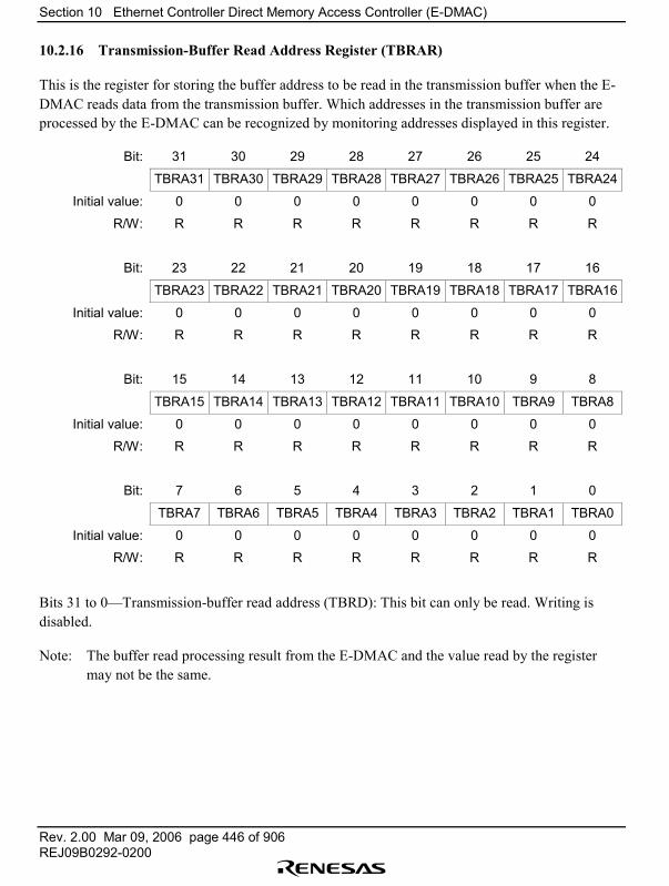
Section 10 Ethernet Controller Direct Memory Access Controller (E-DMAC)
Rev. 2.00 Mar 09, 2006 page 446 of 906REJ09B0292-0200
10.2.16 Transmission-Buffer Read Address Register (TBRAR)
This is the register for storing the buffer address to be read in the transmission buffer when the E-DMAC reads data from the transmission buffer. Which addresses in the transmission buffer areprocessed by the E-DMAC can be recognized by monitoring addresses displayed in this register.
Bit: 31 30 29 28 27 26 25 24
TBRA31 TBRA30 TBRA29 TBRA28 TBRA27 TBRA26 TBRA25 TBRA24
Initial value: 0 0 0 0 0 0 0 0
R/W: R R R R R R R R
Bit: 23 22 21 20 19 18 17 16
TBRA23 TBRA22 TBRA21 TBRA20 TBRA19 TBRA18 TBRA17 TBRA16
Initial value: 0 0 0 0 0 0 0 0
R/W: R R R R R R R R
Bit: 15 14 13 12 11 10 9 8
TBRA15 TBRA14 TBRA13 TBRA12 TBRA11 TBRA10 TBRA9 TBRA8
Initial value: 0 0 0 0 0 0 0 0
R/W: R R R R R R R R
Bit: 7 6 5 4 3 2 1 0
TBRA7 TBRA6 TBRA5 TBRA4 TBRA3 TBRA2 TBRA1 TBRA0
Initial value: 0 0 0 0 0 0 0 0
R/W: R R R R R R R R
Bits 31 to 0�Transmission-buffer read address (TBRD): This bit can only be read. Writing isdisabled.
Note: The buffer read processing result from the E-DMAC and the value read by the registermay not be the same.
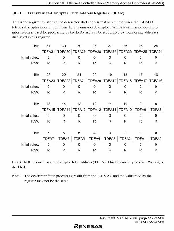
Section 10 Ethernet Controller Direct Memory Access Controller (E-DMAC)
Rev. 2.00 Mar 09, 2006 page 447 of 906REJ09B0292-0200
10.2.17 Transmission-Descriptor Fetch Address Register (TDFAR)
This is the register for storing the descriptor start address that is required when the E-DMACfetches descriptor information from the transmission descriptor . Which transmission descriptorinformation is used for processing by the E-DMAC can be recognized by monitoring addressesdisplayed in this register.
Bit: 31 30 29 28 27 26 25 24
TDFA31 TDFA30 TDFA29 TDFA28 TDFA27 TDFA26 TDFA25 TDFA24
Initial value: 0 0 0 0 0 0 0 0
R/W: R R R R R R R R
Bit: 23 22 21 20 19 18 17 16
TDFA23 TDFA22 TDFA21 TDFA20 TDFA19 TDFA18 TDFA17 TDFA16
Initial value: 0 0 0 0 0 0 0 0
R/W: R R R R R R R R
Bit: 15 14 13 12 11 10 9 8
TDFA15 TDFA14 TDFA13 TDFA12 TDFA11 TDFA10 TDFA9 TDFA8
Initial value: 0 0 0 0 0 0 0 0
R/W: R R R R R R R R
Bit: 7 6 5 4 3 2 1 0
TDFA7 TDFA6 TDFA5 TDFA4 TDFA3 TDFA2 TDFA1 TDFA0
Initial value: 0 0 0 0 0 0 0 0
R/W: R R R R R R R R
Bits 31 to 0�Transmission-descriptor fetch address (TDFA): This bit can only be read. Writing isdisabled.
Note: The descriptor fetch processing result from the E-DMAC and the value read by theregister may not be the same.
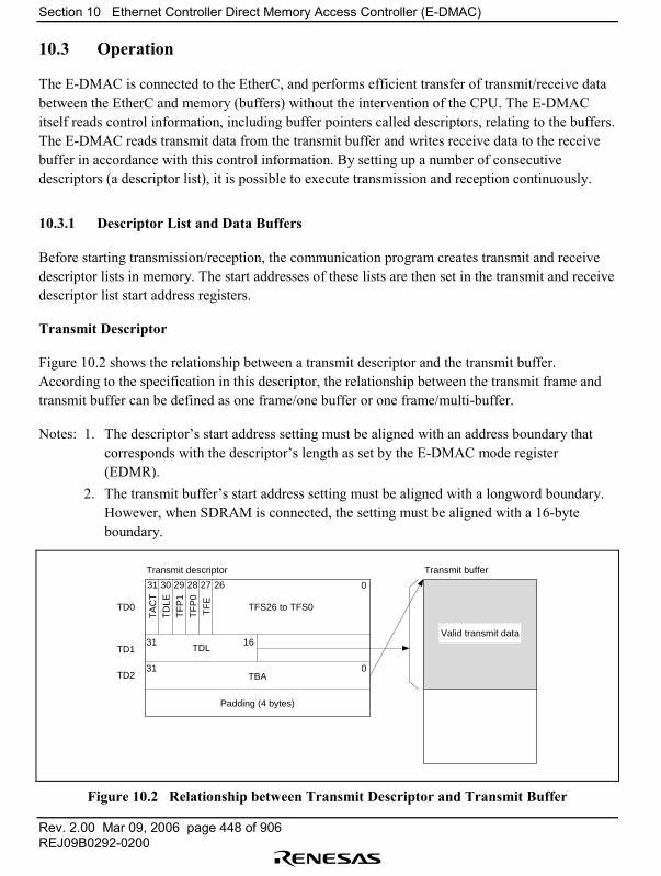
Section 10 Ethernet Controller Direct Memory Access Controller (E-DMAC)
Rev. 2.00 Mar 09, 2006 page 448 of 906REJ09B0292-0200
10.3 Operation
The E-DMAC is connected to the EtherC, and performs efficient transfer of transmit/receive databetween the EtherC and memory (buffers) without the intervention of the CPU. The E-DMACitself reads control information, including buffer pointers called descriptors, relating to the buffers.The E-DMAC reads transmit data from the transmit buffer and writes receive data to the receivebuffer in accordance with this control information. By setting up a number of consecutivedescriptors (a descriptor list), it is possible to execute transmission and reception continuously.
10.3.1 Descriptor List and Data Buffers
Before starting transmission/reception, the communication program creates transmit and receivedescriptor lists in memory. The start addresses of these lists are then set in the transmit and receivedescriptor list start address registers.
Transmit Descriptor
Figure 10.2 shows the relationship between a transmit descriptor and the transmit buffer.According to the specification in this descriptor, the relationship between the transmit frame andtransmit buffer can be defined as one frame/one buffer or one frame/multi-buffer.
Notes: 1. The descriptor�s start address setting must be aligned with an address boundary thatcorresponds with the descriptor�s length as set by the E-DMAC mode register(EDMR).
2. The transmit buffer�s start address setting must be aligned with a longword boundary.However, when SDRAM is connected, the setting must be aligned with a 16-byteboundary.
Transmit descriptor Transmit buffer
TA
CT
TD
LET
FP
1T
FP
0T
FE
TFS26 to TFS0
0
031
1631
31 30 29 28 27 26
TD0
TDLTD1
TBA
Padding (4 bytes)
TD2
Valid transmit data
Figure 10.2 Relationship between Transmit Descriptor and Transmit Buffer
Section 10 Ethernet Controller Direct Memory Access Controller (E-DMAC)
Rev. 2.00 Mar 09, 2006 page 449 of 906REJ09B0292-0200
Transmit Descriptor 0 (TD0): TD0 indicates the transmit frame status. The CPU and E-DMACuse TD0 to report the frame transmission status.
Bit 31�Transmit Descriptor Active (TACT): Indicates that this descriptor is active. The CPU setsthis bit after transmit data has been transferred to the transmit buffer. The E-DMAC resets this biton completion of a frame transfer or when transmission is suspended.
Bit 31: TACT Description
0 The transmit descriptor is invalid
Indicates that valid data has not been written to the transmit buffer by the CPU,or this bit has been reset by a write-back operation on termination of E-DMACframe transfer processing (completion or suspension of transmission)
If this state is recognized in an E-DMAC descriptor read, the E-DMACterminates transmit processing and transmit operations cannot be continued (arestart is necessary)
1 The transmit descriptor is valid
Indicates that valid data has been written to the transmit buffer by the CPU andframe transfer processing has not yet been executed, or that frame transfer isin progress
When this state is recognized in an E-DMAC descriptor read, the E-DMACcontinues with the transmit operation
Bit 30�Transmit Descriptor List Last (TDLE): Indicates that this descriptor is the last in thetransmit descriptor list. After completion of the corresponding buffer transfer, the E-DMACreferences the first descriptor. This specification is used to set a ring configuration for the transmitdescriptors.
Bit 30: TDLE Description
0 This is not the last transmit descriptor list
1 This is the last transmit descriptor list
Bits 29 and 28�Transmit Frame Position 1, 0 (TFP1, TFP0): These two bits specify therelationship between the transmit buffer and transmit frame.

Section 10 Ethernet Controller Direct Memory Access Controller (E-DMAC)
Rev. 2.00 Mar 09, 2006 page 450 of 906REJ09B0292-0200
Bit 29:TFP1
Bit 28:TFP0 Description
0 0 Frame transmission for transmit buffer indicated by this descriptor continues(frame is not concluded)
1 Transmit buffer indicated by this descriptor contains end of frame (frame isconcluded)
1 0 Transmit buffer indicated by this descriptor is start of frame (frame is notconcluded)
1 Contents of transmit buffer indicated by this descriptor are equivalent to oneframe (one frame/one buffer)
Note: In the preceding and following descriptors, a logically positive relationship must bemaintained between the settings of this bit and the TDLE bit.
Bit 27�Transmit Frame Error (TFE): Indicates that one or other bit of the transmit frame statusindicated by bits 26 to 0 is set.
Bit 27: TFE Description
0 No error during transmission
1 An error of some kind occurred during transmission (see bits 26 to 0)
Bits 26 to 0�Transmit Frame Status 26 to 0 (TFS26 to TFS0): These bits indicate the error statusduring frame transmission.
• TFS26 to TFS9�Reserved• TFS8�Teransmit Abort Detect
Note: This bit is set to 1 when any of Transmit Frame Status bits 4 to 0 is set. When this bit isset, the Transmit Frame Error bit (bit 27: TFE) is set to 1.
• TFS7 to TFS5�Reserved• TFS4�Illegal Transmit Frame (corresponds to ITF bit in EESR)• TFS3�Carrier Not Detect (corresponds to CND bit in EESR)• TFS2�Detect Loss of Carrier (corresponds to DLC bit in EESR)• TFS1�Collision Detect (corresponds to CD bit in EESR)• TFS0�Transmit Retry Over (corresponds to TRO bit in EESR)
Section 10 Ethernet Controller Direct Memory Access Controller (E-DMAC)
Rev. 2.00 Mar 09, 2006 page 451 of 906REJ09B0292-0200
Transmit Descriptor 1 (TD1): Specifies the transmit buffer length (maximum 64 kbytes).
Bits 31 to 16�Transmit Buffer Data Length (TDL): These bits specify the valid transfer bytelength in the corresponding transmit buffer.
Note: When the one frame/multi-buffer system is specified (TD0 and TFP = 10 or 00), thetransfer byte length specified in the descriptors at the start and midway can be set in byteunits.
Bits 15 to 0�Reserved: The bits are always read as 0. The write value should always be 0.
Transmit Descriptor 2 (TD2): Specifies the 32-bit transmit buffer start address.
Note: The transmit buffer�s start address setting must be aligned with a longword boundary.However, when SDRAM is connected, the setting must be aligned with a 16-byteboundary.
Bits 31 to 0�Transmit Buffer Address (TBA)
Receive Descriptor
Figure 10.3 shows the relationship between a receive descriptor and the receive buffer. In framereception, the E-DMAC performs data rewriting up to a receive buffer 16-byte boundary,regardless of the receive frame length. Finally, the actual receive frame length is reported in thelower 16 bits of RD1 in the descriptor. Data transfer to the receive buffer is performedautomatically by the E-DMAC to give a one frame/one buffer or one frame/multi-bufferconfiguration according to the size of one received frame.
Notes: 1. The descriptor�s start address setting must be aligned with an address boundary thatcorresponds with the descriptor�s length as set by the E-DMAC mode register(EDMR).
2. The receive buffer�s start address setting must be aligned with a longword boundary.However, when SDRAM is connected, the setting must be aligned with a 16-byteboundary. Make the setting so that the size of the receive buffer is aligned with a 16-byte boundary.Example: H'0500 (= 1280 bytes)
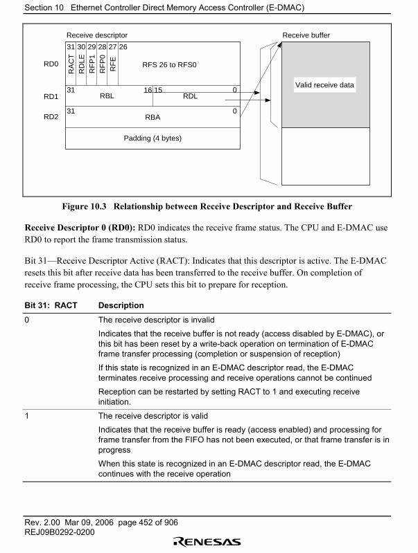
Section 10 Ethernet Controller Direct Memory Access Controller (E-DMAC)
Rev. 2.00 Mar 09, 2006 page 452 of 906REJ09B0292-0200
Receive descriptor Receive buffer
RA
CT
RD
LER
FP
1R
FP
0R
FE
RFS 26 to RFS0RD0
RBL RDL0
0
31
31 30 29 28 2627
31
RD1
RBA
Padding (4 bytes)
RD2
Valid receive data16 15
Figure 10.3 Relationship between Receive Descriptor and Receive Buffer
Receive Descriptor 0 (RD0): RD0 indicates the receive frame status. The CPU and E-DMAC useRD0 to report the frame transmission status.
Bit 31�Receive Descriptor Active (RACT): Indicates that this descriptor is active. The E-DMACresets this bit after receive data has been transferred to the receive buffer. On completion ofreceive frame processing, the CPU sets this bit to prepare for reception.
Bit 31: RACT Description
0 The receive descriptor is invalid
Indicates that the receive buffer is not ready (access disabled by E-DMAC), orthis bit has been reset by a write-back operation on termination of E-DMACframe transfer processing (completion or suspension of reception)
If this state is recognized in an E-DMAC descriptor read, the E-DMACterminates receive processing and receive operations cannot be continued
Reception can be restarted by setting RACT to 1 and executing receiveinitiation.
1 The receive descriptor is valid
Indicates that the receive buffer is ready (access enabled) and processing forframe transfer from the FIFO has not been executed, or that frame transfer is inprogress
When this state is recognized in an E-DMAC descriptor read, the E-DMACcontinues with the receive operation
Section 10 Ethernet Controller Direct Memory Access Controller (E-DMAC)
Rev. 2.00 Mar 09, 2006 page 453 of 906REJ09B0292-0200
Bit 30�Receive Descriptor List Last (RDLE): Indicates that this descriptor is the last in thereceive descriptor list. After completion of the corresponding buffer transfer, the E-DMACreferences the first receive descriptor. This specification is used to set a ring configuration for thereceive descriptors.
Bit 30: RDLE Description
0 This is not the last receive descriptor list
1 This is the last receive descriptor list (the next descriptor is inactive)
Bits 29 and 28�Receive Frame Position 1, 0 (RFP1, RFP0): These two bits specify therelationship between the receive buffer and receive frame.
Bit 29:RFP
Bit 28:RFP Description
0 0 Frame reception for receive buffer indicated by this descriptor continues(frame is not concluded)
1 Receive buffer indicated by this descriptor contains end of frame (frame isconcluded)
1 0 Receive buffer indicated by this descriptor is start of frame (frame is notconcluded)
1 Contents of receive buffer indicated by this descriptor are equivalent to oneframe (one frame/one buffer)
Bit 27�Receive Frame Error (RFE): Indicates that one or other bit of the receive frame statusindicated by bits 26 to 0 is set. Whether or not the multicast address frame receive informationwhich is part of the frame status, is copied into this bit is specified by the transmit/receive statuscopy enable register.
Bit 27: RFE Description
0 No error during reception (Initial value)
1 An error of some kind occurred during reception (see bits 26 to 0)
Bits 26 to 0�Receive Frame Status 26 to 0 (RFS26 to RFS0): These bits indicate the error statusduring frame reception.
• RFS26 to RFS10�Reserved• RFS9�Receive FIFO Overflow (corresponds to RFOF bit in EESR)• RFS8�Reserve Abort Detect
Section 10 Ethernet Controller Direct Memory Access Controller (E-DMAC)
Rev. 2.00 Mar 09, 2006 page 454 of 906REJ09B0292-0200
Note: This bit is set to 1 when any of Receive Frame Status bit 9, bit 7, bits 4 to 0 is set.When this bit is set, the Receive Frame Error bit (bit 27: RFE) is set to 1.
• RFS7�Receive Multicast Address Frame (corresponds to RMAF bit in EESR)• RFS6�Reserved*1
• RSF5� Receive Frame Discard Request Assertion (corresponds to RFAR bit in EESR)*1
• RFS4�Receive Residual-Bit Frame (corresponds to RRF bit in EESR)• RFS3�Receive Too-Long Frame (corresponds to RTLF bit in EESR)• RFS2�Receive Too-Short Frame (corresponds to RTSF bit in EESR)• RFS1�PHY-LSI Receive Error (corresponds to PRE bit in EESR)• RFS0�CRC Error on Received Frame (corresponds to CERF bit in EESR)
Note: 1. Only HD6417616 is effective. HD6417615 is Reserved bit.
Receive Descriptor 1 (RD1): Specifies the receive buffer length (maximum 64 kbytes).
Bits 31 to 16�Receive Buffer Length (RBL): These bits specify the maximum transfer bytelength in the corresponding receive buffer.
Notes: The transfer byte length must align with a 16-byte boundary (bits 19 to 16 cleared to 0).The maximum receive frame length with one frame per buffer is 1,514 bytes, excludingthe CRC data. Therefore, for the receive buffer length specification, a value of 1,520 bytes(H'05F0) that takes account of a 16-byte boundary is set as the maximum receive framelength.
Bits 15 to 0�Receive Data Length (RDL): These bits specify the data length of a receive framestored in the receive buffer.
Note: The receive data transferred to the receive buffer does not include the 4-byte CRC data atthe end of the frame. The receive frame length is reported as the number of words (validdata bytes) not including this CRC data.
Receive Descriptor 2 (RD2): Specifies the 32-bit receive buffer start address.
Note: The receive buffer�s start address setting must be aligned with a longword boundary.However, when SDRAM is connected, the setting must be aligned with a 16-byteboundary.
Bits 31 to 0�Receive Buffer Address (RBA)
Section 10 Ethernet Controller Direct Memory Access Controller (E-DMAC)
Rev. 2.00 Mar 09, 2006 page 455 of 906REJ09B0292-0200
10.3.2 Transmission
When the transmitter is enabled and the transmit request bit (TR) is set in the E-DMAC transmitrequest register (EDTRR), the E-DMAC reads the descriptor used last time from the transmitdescriptor list (in the initial state, the descriptor indicated by the transmission descriptor startaddress register (TDLAR)). If the setting of the TACT bit in the read descriptor is �active,� the E-DMAC reads transmit frame data sequentially from the transmit buffer start address specified byTD2, and transfers it to the EtherC. The EtherC creates a transmit frame and starts transmission tothe MII. After DMA transfer of data equivalent to the buffer length specified in the descriptor, thefollowing processing is carried out according to the TFP value.
1. TFP = 00 or 01 (frame continuation):Descriptor write-back is performed after DMA transfer.
2. TFP = 01 or 11 (frame end):Descriptor write-back is performed after completion of frame transmission.
The E-DMAC continues reading descriptors and transmitting frames as long as the setting of theTACT bit in the read descriptors is �active.� When a descriptor with an �inactive� TACT bit isread, the E-DMAC resets the transmit request bit (TR) in the transmit register and ends transmitprocessing (EDTRR).

Section 10 Ethernet Controller Direct Memory Access Controller (E-DMAC)
Rev. 2.00 Mar 09, 2006 page 456 of 906REJ09B0292-0200
SH7616 + memory
Transmission flowchart
E-DMAC EtherC EthernetTransmit FIFO
EtherC/E-DMACinitialization
Descriptor andtransmit
buffer setting
Transmit directive
Descriptor read
Descriptor write-back
Descriptor write-back
Transmission completed
Descriptor read
Transmit data transfer
Transmit data transfer
Frame transmission
Figure 10.4 Sample Transmission Flowchart
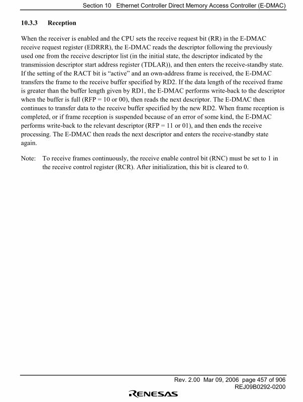
Section 10 Ethernet Controller Direct Memory Access Controller (E-DMAC)
Rev. 2.00 Mar 09, 2006 page 457 of 906REJ09B0292-0200
10.3.3 Reception
When the receiver is enabled and the CPU sets the receive request bit (RR) in the E-DMACreceive request register (EDRRR), the E-DMAC reads the descriptor following the previouslyused one from the receive descriptor list (in the initial state, the descriptor indicated by thetransmission descriptor start address register (TDLAR)), and then enters the receive-standby state.If the setting of the RACT bit is �active� and an own-address frame is received, the E-DMACtransfers the frame to the receive buffer specified by RD2. If the data length of the received frameis greater than the buffer length given by RD1, the E-DMAC performs write-back to the descriptorwhen the buffer is full (RFP = 10 or 00), then reads the next descriptor. The E-DMAC thencontinues to transfer data to the receive buffer specified by the new RD2. When frame reception iscompleted, or if frame reception is suspended because of an error of some kind, the E-DMACperforms write-back to the relevant descriptor (RFP = 11 or 01), and then ends the receiveprocessing. The E-DMAC then reads the next descriptor and enters the receive-standby stateagain.
Note: To receive frames continuously, the receive enable control bit (RNC) must be set to 1 inthe receive control register (RCR). After initialization, this bit is cleared to 0.
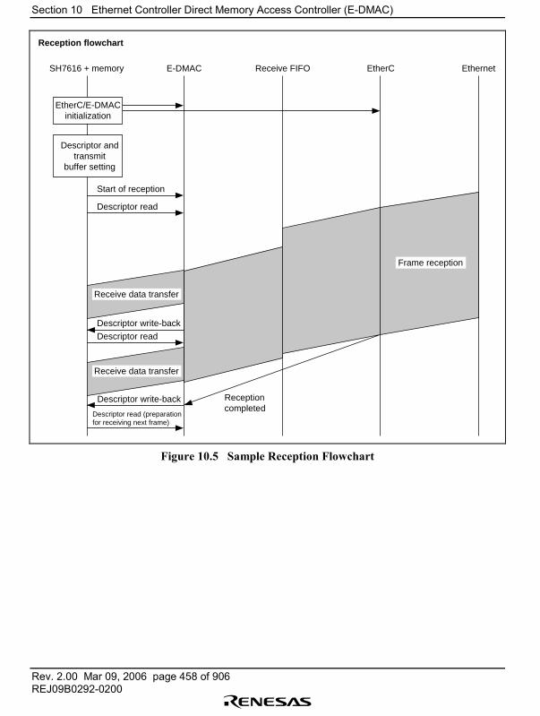
Section 10 Ethernet Controller Direct Memory Access Controller (E-DMAC)
Rev. 2.00 Mar 09, 2006 page 458 of 906REJ09B0292-0200
SH7616 + memory
Reception flowchart
E-DMAC EtherCReceive FIFO Ethernet
EtherC/E-DMACinitialization
Descriptor andtransmit
buffer setting
Reception completed
Receive data transfer
Frame reception
Start of reception
Descriptor read
Descriptor write-back
Descriptor write-back
Descriptor read (preparation for receiving next frame)
Descriptor read
Receive data transfer
Figure 10.5 Sample Reception Flowchart
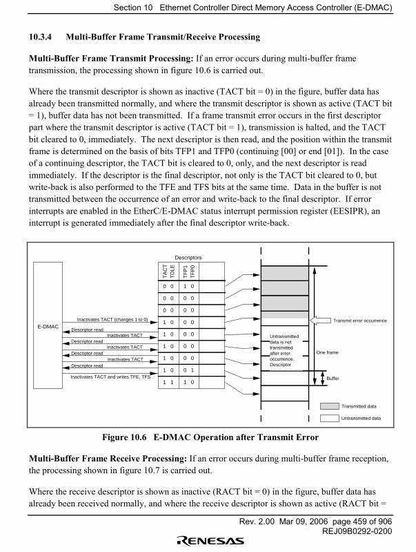
Section 10 Ethernet Controller Direct Memory Access Controller (E-DMAC)
Rev. 2.00 Mar 09, 2006 page 459 of 906REJ09B0292-0200
10.3.4 Multi-Buffer Frame Transmit/Receive Processing
Multi-Buffer Frame Transmit Processing: If an error occurs during multi-buffer frametransmission, the processing shown in figure 10.6 is carried out.
Where the transmit descriptor is shown as inactive (TACT bit = 0) in the figure, buffer data hasalready been transmitted normally, and where the transmit descriptor is shown as active (TACT bit= 1), buffer data has not been transmitted. If a frame transmit error occurs in the first descriptorpart where the transmit descriptor is active (TACT bit = 1), transmission is halted, and the TACTbit cleared to 0, immediately. The next descriptor is then read, and the position within the transmitframe is determined on the basis of bits TFP1 and TFP0 (continuing [00] or end [01]). In the caseof a continuing descriptor, the TACT bit is cleared to 0, only, and the next descriptor is readimmediately. If the descriptor is the final descriptor, not only is the TACT bit cleared to 0, butwrite-back is also performed to the TFE and TFS bits at the same time. Data in the buffer is nottransmitted between the occurrence of an error and write-back to the final descriptor. If errorinterrupts are enabled in the EtherC/E-DMAC status interrupt permission register (EESIPR), aninterrupt is generated immediately after the final descriptor write-back.
0 0
0 0
0 0
1 0
1 0
1 0
1 0
1 0
1 1
1 0
0 0
0 0
0 0
0 0
0 0
0 0
0 1
1 0
E-DMACInactivates TACT (changes 1 to 0)
Descriptor read
Descriptor read
Descriptor read
Descriptor read Inactivates TACT
Inactivates TACT
Inactivates TACT
Inactivates TACT and writes TFE, TFS
Descriptors
One frame
Buffer
Transmitted data
Untransmitted data
Transmit error occurrence
Untransmitted data is not transmitted after error occurrence. Descriptor
TA
CT
TD
LE
TF
P1
TF
P0
Figure 10.6 E-DMAC Operation after Transmit Error
Multi-Buffer Frame Receive Processing: If an error occurs during multi-buffer frame reception,the processing shown in figure 10.7 is carried out.
Where the receive descriptor is shown as inactive (RACT bit = 0) in the figure, buffer data hasalready been received normally, and where the receive descriptor is shown as active (RACT bit =
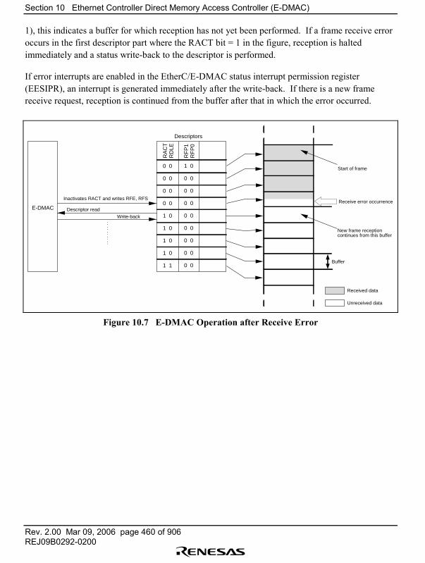
Section 10 Ethernet Controller Direct Memory Access Controller (E-DMAC)
Rev. 2.00 Mar 09, 2006 page 460 of 906REJ09B0292-0200
1), this indicates a buffer for which reception has not yet been performed. If a frame receive erroroccurs in the first descriptor part where the RACT bit = 1 in the figure, reception is haltedimmediately and a status write-back to the descriptor is performed.
If error interrupts are enabled in the EtherC/E-DMAC status interrupt permission register(EESIPR), an interrupt is generated immediately after the write-back. If there is a new framereceive request, reception is continued from the buffer after that in which the error occurred.
0 0
0 0
0 0
0 0
1 0
1 0
1 0
1 0
1 1
1 0
0 0
0 0
0 0
0 0
0 0
0 0
0 0
0 0
E-DMAC
Inactivates RACT and writes RFE, RFS
Descriptor read
Write-back
Descriptors
Buffer
Received data
Unreceived data
Receive error occurrence
:::::
Start of frame
New frame reception continues from this buffer
RA
CT
RD
LE
RF
P1
RF
P0
Figure 10.7 E-DMAC Operation after Receive Error

Section 11 Direct Memory Access Controller (DMAC)
Rev. 2.00 Mar 09, 2006 page 461 of 906REJ09B0292-0200
Section 11 Direct Memory Access Controller (DMAC)
11.1 Overview
A two-channel direct memory access controller (DMAC) is included on-chip. The DMAC can beused in place of the CPU to perform high-speed data transfers between external devices equippedwith DACK (transfer request acknowledge signal), external memories, on-chip memory, andmemory-mapped external devices. Using the DMAC reduces the burden on the CPU and increasesthe operating efficiency of the chip as a whole.
11.1.1 Features
The DMAC has the following features:
• Two channels• Address space: Architecturally 4 Gbytes• Choice of data transfer unit: Byte, word (2-byte), longword (4-byte) or 16-byte unit (In a 16-
byte transfer, four longword reads are executed, followed by four longword writes.)• Maximum of 16,777,216 (16M) transfers• In the event of a cache hit, CPU instruction processing and DMA operation can be executed in
parallel• Single address mode transfers: Either the transfer source or transfer destination (peripheral
device) is accessed by a DACK signal (selectable) while the other is accessed by address. Onetransfer unit of data is transferred in one bus cycle.Possible transfer devices: External devices with DACK and memory-mapped external devices(including external memory)
• Dual address mode transfer: Both the transfer source and transfer destination are accessed byaddress. One transfer unit of data is transferred in two bus cycles.Possible transfer devices: Two external memories External memory and memory-mapped external device Two memory-mapped external devices External memory and on-chip peripheral module (excluding DMAC, BSC, UBC, cache-
memory, E-DMAC, and EtherC) Memory-mapped external device and on-chip peripheral module (excluding DMAC, BSC,
UBC, cache-memory, E-DMAC, and EtherC)
Section 11 Direct Memory Access Controller (DMAC)
Rev. 2.00 Mar 09, 2006 page 462 of 906REJ09B0292-0200
Two on-chip peripheral modules (excluding DMAC, BSC, UBC, cache-memory, E-DMAC, and EtherC)
On-chip memory and memory-mapped external device Two on-chip memories On-chip memory and on-chip peripheral modules (excluding DMAC, BSC, UBC, cache-
memory, E-DMAC, and EtherC) On-chip memory and external memory
• Transfer requests External request: from the DREQn pins. Edge or level detection, and active-low or active-
high mode, can be specified for DREQn. On-chip peripheral module requests: serial communication interface with FIFO (SCIF),
16-bit timer pulse unit (TPU), serial I/O with FIFO (SIOF), serial I/O (SIO) Auto-request: the transfer request is generated automatically within the DMAC
• Choice of bus mode Cycle steal mode Burst mode
• Choice of channel priority order Fixed mode Round robin mode
• An interrupt request can be sent to the CPU on completion of data transfer
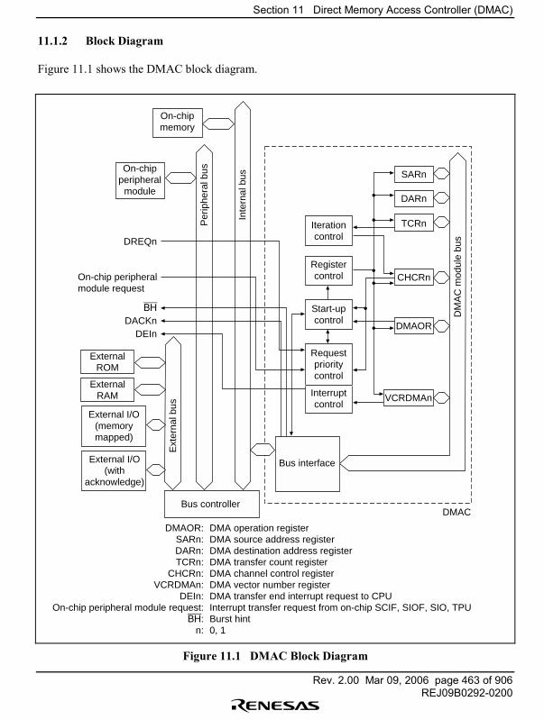
Section 11 Direct Memory Access Controller (DMAC)
Rev. 2.00 Mar 09, 2006 page 463 of 906REJ09B0292-0200
11.1.2 Block Diagram
Figure 11.1 shows the DMAC block diagram.
DREQn
On-chip peripheralmodule request
DACKnBH
DEIn
DMAC
On-chipperipheral
module
On-chipmemory
Per
iphe
ral b
us
Ext
erna
l bus
ExternalROM
ExternalRAM
External I/O(memorymapped)
External I/O(with
acknowledge)
Bus controller
Iterationcontrol
Registercontrol
Start-upcontrol
Requestprioritycontrol
Interruptcontrol
Bus interfaceD
MA
C m
odul
e bu
s
SARn
DARn
TCRn
CHCRn
DMAOR
VCRDMAn
Inte
rnal
bus
DMAOR: SARn: DARn: TCRn:
CHCRn: VCRDMAn:
DEIn:On-chip peripheral module request:
BH: n:
DMA operation registerDMA source address registerDMA destination address registerDMA transfer count registerDMA channel control registerDMA vector number registerDMA transfer end interrupt request to CPUInterrupt transfer request from on-chip SCIF, SIOF, SIO, TPUBurst hint0, 1
Figure 11.1 DMAC Block Diagram
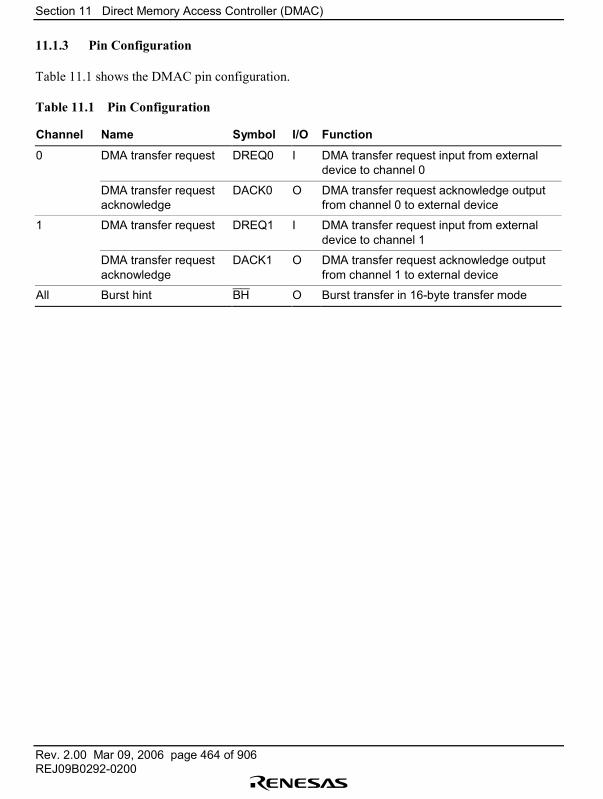
Section 11 Direct Memory Access Controller (DMAC)
Rev. 2.00 Mar 09, 2006 page 464 of 906REJ09B0292-0200
11.1.3 Pin Configuration
Table 11.1 shows the DMAC pin configuration.
Table 11.1 Pin Configuration
Channel Name Symbol I/O Function
0 DMA transfer request DREQ0 I DMA transfer request input from externaldevice to channel 0
DMA transfer requestacknowledge
DACK0 O DMA transfer request acknowledge outputfrom channel 0 to external device
1 DMA transfer request DREQ1 I DMA transfer request input from externaldevice to channel 1
DMA transfer requestacknowledge
DACK1 O DMA transfer request acknowledge outputfrom channel 1 to external device
All Burst hint BH O Burst transfer in 16-byte transfer mode
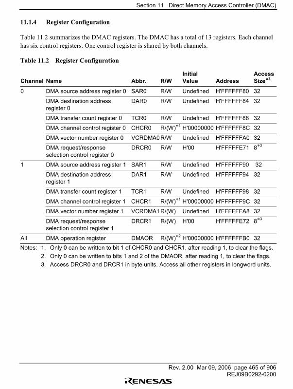
Section 11 Direct Memory Access Controller (DMAC)
Rev. 2.00 Mar 09, 2006 page 465 of 906REJ09B0292-0200
11.1.4 Register Configuration
Table 11.2 summarizes the DMAC registers. The DMAC has a total of 13 registers. Each channelhas six control registers. One control register is shared by both channels.
Table 11.2 Register Configuration
Channel Name Abbr. R/WInitialValue Address
AccessSize*3
0 DMA source address register 0 SAR0 R/W Undefined H'FFFFFF80 32
DMA destination addressregister 0
DAR0 R/W Undefined H'FFFFFF84 32
DMA transfer count register 0 TCR0 R/W Undefined H'FFFFFF88 32
DMA channel control register 0 CHCR0 R/(W)*1 H'00000000 H'FFFFFF8C 32
DMA vector number register 0 VCRDMA0R/W Undefined H'FFFFFFA0 32
DMA request/responseselection control register 0
DRCR0 R/W H'00 H'FFFFFE71 8*3
1 DMA source address register 1 SAR1 R/W Undefined H'FFFFFF90 32
DMA destination addressregister 1
DAR1 R/W Undefined H'FFFFFF94 32
DMA transfer count register 1 TCR1 R/W Undefined H'FFFFFF98 32
DMA channel control register 1 CHCR1 R/(W)*1 H'00000000 H'FFFFFF9C 32
DMA vector number register 1 VCRDMA1R/(W) Undefined H'FFFFFFA8 32
DMA request/responseselection control register 1
DRCR1 R/(W) H'00 H'FFFFFE72 8*3
All DMA operation register DMAOR R/(W)*2 H'00000000 H'FFFFFFB0 32Notes: 1. Only 0 can be written to bit 1 of CHCR0 and CHCR1, after reading 1, to clear the flags.
2. Only 0 can be written to bits 1 and 2 of the DMAOR, after reading 1, to clear the flags.3. Access DRCR0 and DRCR1 in byte units. Access all other registers in longword units.
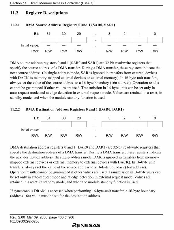
Section 11 Direct Memory Access Controller (DMAC)
Rev. 2.00 Mar 09, 2006 page 466 of 906REJ09B0292-0200
11.2 Register Descriptions
11.2.1 DMA Source Address Registers 0 and 1 (SAR0, SAR1)
Bit: 31 30 29 � 3 2 1 0
�
Initial value: � � � � � � � �
R/W: R/W R/W R/W � R/W R/W R/W R/W
DMA source address registers 0 and 1 (SAR0 and SAR1) are 32-bit read/write registers thatspecify the source address of a DMA transfer. During a DMA transfer, these registers indicate thenext source address. (In single-address mode, SAR is ignored in transfers from external deviceswith DACK to memory-mapped external devices or external memory). In 16-byte unit transfers,always set the value of the source address to a 16-byte boundary (16n address). Operation resultscannot be guaranteed if other values are used. Transmission in 16-byte units can be set only inauto-request mode and at edge detection in external request mode. Values are retained in a reset, instandby mode, and when the module standby function is used.
11.2.2 DMA Destination Address Registers 0 and 1 (DAR0, DAR1)
Bit: 31 30 29 � 3 2 1 0
�
Initial value: � � � � � � � �
R/W: R/W R/W R/W � R/W R/W R/W R/W
DMA destination address registers 0 and 1 (DAR0 and DAR1) are 32-bit read/write registers thatspecify the destination address of a DMA transfer. During a DMA transfer, these registers indicatethe next destination address. (In single-address mode, DAR is ignored in transfers from memory-mapped external devices or external memory to external devices with DACK). In 16-byte unittransfers, always set the value of the source address to a 16-byte boundary (16n address).Operation results cannot be guaranteed if other values are used. Transmission in 16-byte units canbe set only in auto-request mode and at edge detection in external request mode. Values areretained in a reset, in standby mode, and when the module standby function is used.
If synchronous DRAM is accessed when performing 16-byte-unit transfer, a 16-byte boundary(address 16n) value must be set for the destination address.
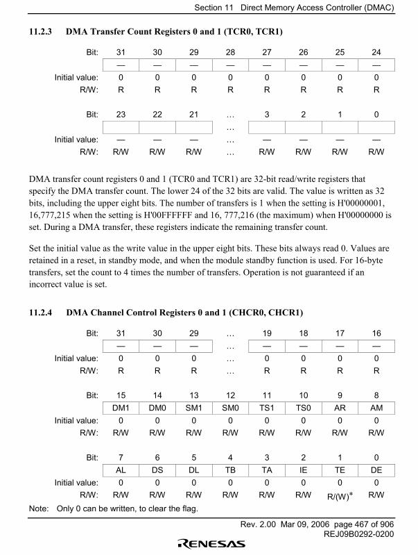
Section 11 Direct Memory Access Controller (DMAC)
Rev. 2.00 Mar 09, 2006 page 467 of 906REJ09B0292-0200
11.2.3 DMA Transfer Count Registers 0 and 1 (TCR0, TCR1)
Bit: 31 30 29 28 27 26 25 24� � � � � � � �
Initial value: 0 0 0 0 0 0 0 0R/W: R R R R R R R R
Bit: 23 22 21 � 3 2 1 0�
Initial value: � � � � � � � �R/W: R/W R/W R/W � R/W R/W R/W R/W
DMA transfer count registers 0 and 1 (TCR0 and TCR1) are 32-bit read/write registers thatspecify the DMA transfer count. The lower 24 of the 32 bits are valid. The value is written as 32bits, including the upper eight bits. The number of transfers is 1 when the setting is H'00000001,16,777,215 when the setting is H'00FFFFFF and 16, 777,216 (the maximum) when H'00000000 isset. During a DMA transfer, these registers indicate the remaining transfer count.
Set the initial value as the write value in the upper eight bits. These bits always read 0. Values areretained in a reset, in standby mode, and when the module standby function is used. For 16-bytetransfers, set the count to 4 times the number of transfers. Operation is not guaranteed if anincorrect value is set.
11.2.4 DMA Channel Control Registers 0 and 1 (CHCR0, CHCR1)
Bit: 31 30 29 � 19 18 17 16� � � � � � � �
Initial value: 0 0 0 � 0 0 0 0R/W: R R R � R R R R
Bit: 15 14 13 12 11 10 9 8DM1 DM0 SM1 SM0 TS1 TS0 AR AM
Initial value: 0 0 0 0 0 0 0 0R/W: R/W R/W R/W R/W R/W R/W R/W R/W
Bit: 7 6 5 4 3 2 1 0AL DS DL TB TA IE TE DE
Initial value: 0 0 0 0 0 0 0 0R/W: R/W R/W R/W R/W R/W R/W R/(W)* R/W
Note: Only 0 can be written, to clear the flag.
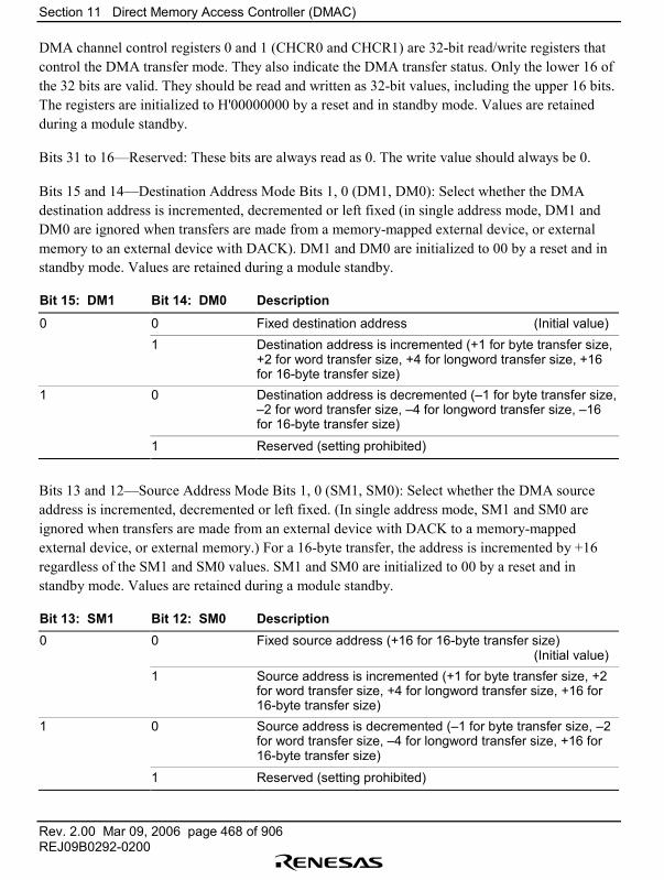
Section 11 Direct Memory Access Controller (DMAC)
Rev. 2.00 Mar 09, 2006 page 468 of 906REJ09B0292-0200
DMA channel control registers 0 and 1 (CHCR0 and CHCR1) are 32-bit read/write registers thatcontrol the DMA transfer mode. They also indicate the DMA transfer status. Only the lower 16 ofthe 32 bits are valid. They should be read and written as 32-bit values, including the upper 16 bits.The registers are initialized to H'00000000 by a reset and in standby mode. Values are retainedduring a module standby.
Bits 31 to 16�Reserved: These bits are always read as 0. The write value should always be 0.
Bits 15 and 14�Destination Address Mode Bits 1, 0 (DM1, DM0): Select whether the DMAdestination address is incremented, decremented or left fixed (in single address mode, DM1 andDM0 are ignored when transfers are made from a memory-mapped external device, or externalmemory to an external device with DACK). DM1 and DM0 are initialized to 00 by a reset and instandby mode. Values are retained during a module standby.
Bit 15: DM1 Bit 14: DM0 Description
0 0 Fixed destination address (Initial value)1 Destination address is incremented (+1 for byte transfer size,
+2 for word transfer size, +4 for longword transfer size, +16for 16-byte transfer size)
1 0 Destination address is decremented (�1 for byte transfer size,�2 for word transfer size, �4 for longword transfer size, �16for 16-byte transfer size)
1 Reserved (setting prohibited)
Bits 13 and 12�Source Address Mode Bits 1, 0 (SM1, SM0): Select whether the DMA sourceaddress is incremented, decremented or left fixed. (In single address mode, SM1 and SM0 areignored when transfers are made from an external device with DACK to a memory-mappedexternal device, or external memory.) For a 16-byte transfer, the address is incremented by +16regardless of the SM1 and SM0 values. SM1 and SM0 are initialized to 00 by a reset and instandby mode. Values are retained during a module standby.
Bit 13: SM1 Bit 12: SM0 Description0 0 Fixed source address (+16 for 16-byte transfer size)
(Initial value)1 Source address is incremented (+1 for byte transfer size, +2
for word transfer size, +4 for longword transfer size, +16 for16-byte transfer size)
1 0 Source address is decremented (�1 for byte transfer size, �2for word transfer size, �4 for longword transfer size, +16 for16-byte transfer size)
1 Reserved (setting prohibited)
Section 11 Direct Memory Access Controller (DMAC)
Rev. 2.00 Mar 09, 2006 page 469 of 906REJ09B0292-0200
Bits 11 and 10�Transfer Size Bits (TS1, TS0): Select the DMA transfer size. When 11 is set tobits TS1 and TS0 (in the 16-byte unit), request mode is available only in auto-request mode and atedge detection in external request mode. When 11 is set to bits TS1 and TS0 (in the 16-byte unit)and level detection in external request mode and internal peripheral-module request mode are set,system operations are not guaranteed. TS1 and TS0 are initialized to 00 by a reset and in standbymode. Values are retained during a module standby.
Bit 11: TS1 Bit 10: TS0 Description
0 0 Byte unit* (initial value)
1 Word (2-byte) unit
1 0 Longword (4-byte) unit
1 16-byte unit (4 longword transfers)Note: * The byte unit setting should not be used if a destination address has been set in internal
memory for the dual address mode.
Bit 9�Auto Request Mode Bit (AR): Selects either auto-request mode (in which transfer requestsare generated automatically within the DMAC) or a mode using external requests or requests fromon-chip peripheral modules (SCIF, TPU, SIOF, SIO). The AR bit is initialized to 0 by a reset andin standby mode. Its value is retained during a module standby.
Bit 9: AR Description
0 External/on-chip peripheral module request mode (Initial value)
1 Auto-request mode
Bit 8�Acknowledge/Transfer Mode Bit (AM): In dual address mode, this bit selects whether theDACKn signal is output during the data read cycle or write cycle. In single-address mode, itselects whether to transfer data from memory to device or from device to memory. The AM bit isinitialized to 0 by a reset and in standby mode. Its value is retained during a module standby.
Bit 8: AM Description
0 DACKn output in read cycle (dual address mode)/transfer from memoryto device (single address mode) (Initial value)
1 DACKn output in write cycle (dual address mode)/transfer from deviceto memory (single address mode)
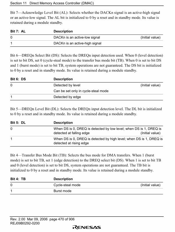
Section 11 Direct Memory Access Controller (DMAC)
Rev. 2.00 Mar 09, 2006 page 470 of 906REJ09B0292-0200
Bit 7�Acknowledge Level Bit (AL): Selects whether the DACKn signal is an active-high signalor an active-low signal. The AL bit is initialized to 0 by a reset and in standby mode. Its value isretained during a module standby.
Bit 7: AL Description
0 DACKn is an active-low signal (Initial value)
1 DACKn is an active-high signal
Bit 6�DREQn Select Bit (DS): Selects the DREQn input detection used. When 0 (level detection)is set to bit DS, set 0 (cycle-steal mode) to the transfer bus mode bit (TB). When 0 is set to bit DSand 1 (burst mode) is set to bit TB, system operations are not guaranteed. The DS bit is initializedto 0 by a reset and in standby mode. Its value is retained during a module standby.
Bit 6: DS Description
0 Detected by level (Initial value)
Can be set only in cycle-steal mode
1 Detected by edge
Bit 5�DREQn Level Bit (DL): Selects the DREQn input detection level. The DL bit is initializedto 0 by a reset and in standby mode. Its value is retained during a module standby.
Bit 5: DL Description
0 When DS is 0, DREQ is detected by low level; when DS is 1, DREQ isdetected at falling edge (Initial value)
1 When DS is 0, DREQ is detected by high level; when DS is 1, DREQ isdetected at rising edge
Bit 4�Transfer Bus Mode Bit (TB): Selects the bus mode for DMA transfers. When 1 (burstmode) is set to bit TB, set 1 (edge detection) to the DREQ select bit (DS). When 1 is set to bit TBand 0 (level detection) is set to bit DS, system operations are not guaranteed. The TB bit isinitialized to 0 by a reset and in standby mode. Its value is retained during a module standby.
Bit 4: TB Description
0 Cycle-steal mode (Initial value)
1 Burst mode
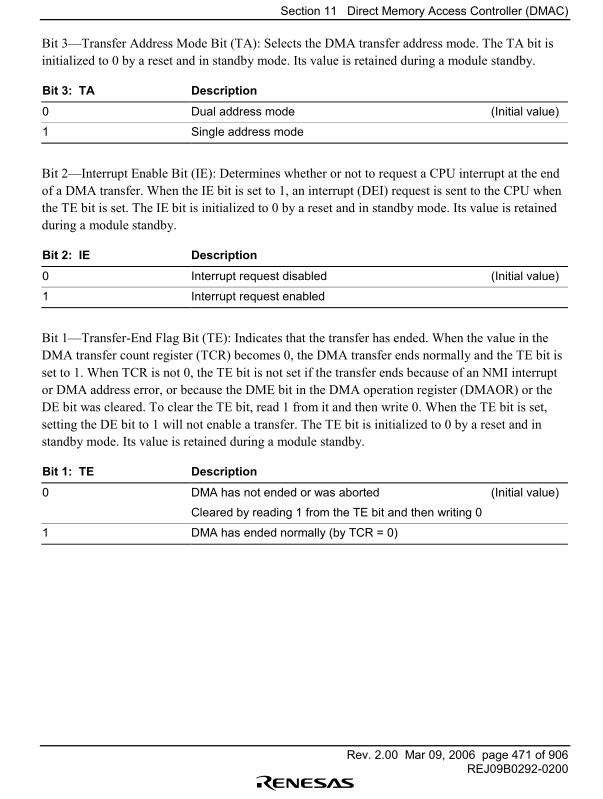
Section 11 Direct Memory Access Controller (DMAC)
Rev. 2.00 Mar 09, 2006 page 471 of 906REJ09B0292-0200
Bit 3�Transfer Address Mode Bit (TA): Selects the DMA transfer address mode. The TA bit isinitialized to 0 by a reset and in standby mode. Its value is retained during a module standby.
Bit 3: TA Description
0 Dual address mode (Initial value)
1 Single address mode
Bit 2�Interrupt Enable Bit (IE): Determines whether or not to request a CPU interrupt at the endof a DMA transfer. When the IE bit is set to 1, an interrupt (DEI) request is sent to the CPU whenthe TE bit is set. The IE bit is initialized to 0 by a reset and in standby mode. Its value is retainedduring a module standby.
Bit 2: IE Description
0 Interrupt request disabled (Initial value)
1 Interrupt request enabled
Bit 1�Transfer-End Flag Bit (TE): Indicates that the transfer has ended. When the value in theDMA transfer count register (TCR) becomes 0, the DMA transfer ends normally and the TE bit isset to 1. When TCR is not 0, the TE bit is not set if the transfer ends because of an NMI interruptor DMA address error, or because the DME bit in the DMA operation register (DMAOR) or theDE bit was cleared. To clear the TE bit, read 1 from it and then write 0. When the TE bit is set,setting the DE bit to 1 will not enable a transfer. The TE bit is initialized to 0 by a reset and instandby mode. Its value is retained during a module standby.
Bit 1: TE Description
0 DMA has not ended or was aborted (Initial value)
Cleared by reading 1 from the TE bit and then writing 0
1 DMA has ended normally (by TCR = 0)
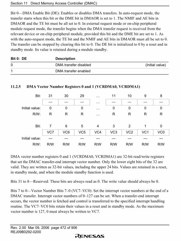
Section 11 Direct Memory Access Controller (DMAC)
Rev. 2.00 Mar 09, 2006 page 472 of 906REJ09B0292-0200
Bit 0�DMA Enable Bit (DE): Enables or disables DMA transfers. In auto-request mode, thetransfer starts when this bit or the DME bit in DMAOR is set to 1. The NMIF and AE bits inDMAOR and the TE bit must be all set to 0. In external request mode or on-chip peripheralmodule request mode, the transfer begins when the DMA transfer request is received from therelevant device or on-chip peripheral module, provided this bit and the DME bit are set to 1. Aswith the auto-request mode, the TE bit and the NMIF and AE bits in DMAOR must all be set to 0.The transfer can be stopped by clearing this bit to 0. The DE bit is initialized to 0 by a reset and instandby mode. Its value is retained during a module standby.
Bit 0: DE Description
0 DMA transfer disabled (Initial value)
1 DMA transfer enabled
11.2.5 DMA Vector Number Registers 0 and 1 (VCRDMA0, VCRDMA1)
Bit: 31 30 29 � 11 10 9 8
� � � � � � � �
Initial value: 0 0 0 � 0 0 0 0
R/W: R R R � R R R R
Bit: 7 6 5 4 3 2 1 0
VC7 VC6 VC5 VC4 VC3 VC2 VC1 VC0
Initial value: � � � � � � � �
R/W: R/W R/W R/W R/W R/W R/W R/W R/W
DMA vector number registers 0 and 1 (VCRDMA0, VCRDMA1) are 32-bit read/write registersthat set the DMAC transfer-end interrupt vector number. Only the lower eight bits of the 32 arevalid. They are written as 32-bit values, including the upper 24 bits. Values are retained in a reset,in standby mode, and when the module standby function is used.
Bits 31 to 8�Reserved: These bits are always read as 0. The write value should always be 0.
Bits 7 to 0�Vector Number Bits 7�0 (VC7�VC0): Set the interrupt vector numbers at the end of aDMAC transfer. Interrupt vector numbers of 0�127 can be set. When a transfer-end interruptoccurs, the vector number is fetched and control is transferred to the specified interrupt handlingroutine. The VC7�VC0 bits retain their values in a reset and in standby mode. As the maximumvector number is 127, 0 must always be written to VC7.
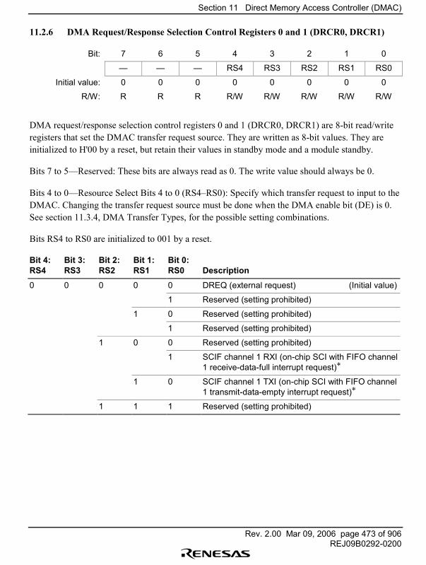
Section 11 Direct Memory Access Controller (DMAC)
Rev. 2.00 Mar 09, 2006 page 473 of 906REJ09B0292-0200
11.2.6 DMA Request/Response Selection Control Registers 0 and 1 (DRCR0, DRCR1)
Bit: 7 6 5 4 3 2 1 0
� � � RS4 RS3 RS2 RS1 RS0
Initial value: 0 0 0 0 0 0 0 0
R/W: R R R R/W R/W R/W R/W R/W
DMA request/response selection control registers 0 and 1 (DRCR0, DRCR1) are 8-bit read/writeregisters that set the DMAC transfer request source. They are written as 8-bit values. They areinitialized to H'00 by a reset, but retain their values in standby mode and a module standby.
Bits 7 to 5�Reserved: These bits are always read as 0. The write value should always be 0.
Bits 4 to 0�Resource Select Bits 4 to 0 (RS4�RS0): Specify which transfer request to input to theDMAC. Changing the transfer request source must be done when the DMA enable bit (DE) is 0.See section 11.3.4, DMA Transfer Types, for the possible setting combinations.
Bits RS4 to RS0 are initialized to 001 by a reset.
Bit 4:RS4
Bit 3:RS3
Bit 2:RS2
Bit 1:RS1
Bit 0:RS0 Description
0 0 0 0 0 DREQ (external request) (Initial value)
1 Reserved (setting prohibited)
1 0 Reserved (setting prohibited)
1 Reserved (setting prohibited)
1 0 0 Reserved (setting prohibited)
1 SCIF channel 1 RXI (on-chip SCI with FIFO channel1 receive-data-full interrupt request)*
1 0 SCIF channel 1 TXI (on-chip SCI with FIFO channel1 transmit-data-empty interrupt request)*
1 1 1 Reserved (setting prohibited)
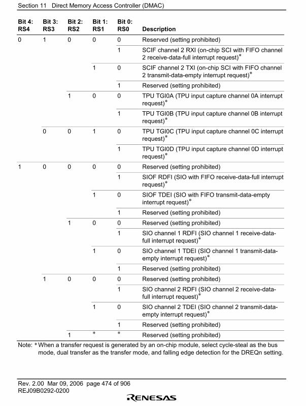
Section 11 Direct Memory Access Controller (DMAC)
Rev. 2.00 Mar 09, 2006 page 474 of 906REJ09B0292-0200
Bit 4:RS4
Bit 3:RS3
Bit 2:RS2
Bit 1:RS1
Bit 0:RS0 Description
0 1 0 0 0 Reserved (setting prohibited)
1 SCIF channel 2 RXI (on-chip SCI with FIFO channel2 receive-data-full interrupt request)*
1 0 SCIF channel 2 TXI (on-chip SCI with FIFO channel2 transmit-data-empty interrupt request)*
1 Reserved (setting prohibited)
1 0 0 TPU TGI0A (TPU input capture channel 0A interruptrequest)*
1 TPU TGI0B (TPU input capture channel 0B interruptrequest)*
0 0 1 0 TPU TGI0C (TPU input capture channel 0C interruptrequest)*
1 TPU TGI0D (TPU input capture channel 0D interruptrequest)*
1 0 0 0 0 Reserved (setting prohibited)
1 SIOF RDFI (SIO with FIFO receive-data-full interruptrequest)*
1 0 SIOF TDEI (SIO with FIFO transmit-data-emptyinterrupt request)*
1 Reserved (setting prohibited)
1 0 0 Reserved (setting prohibited)
1 SIO channel 1 RDFI (SIO channel 1 receive-data-full interrupt request)*
1 0 SIO channel 1 TDEI (SIO channel 1 transmit-data-empty interrupt request)*
1 Reserved (setting prohibited)
1 0 0 0 Reserved (setting prohibited)
1 SIO channel 2 RDFI (SIO channel 2 receive-data-full interrupt request)*
1 0 SIO channel 2 TDEI (SIO channel 2 transmit-data-empty interrupt request)*
1 Reserved (setting prohibited)
1 * * Reserved (setting prohibited)Note: * When a transfer request is generated by an on-chip module, select cycle-steal as the bus
mode, dual transfer as the transfer mode, and falling edge detection for the DREQn setting.
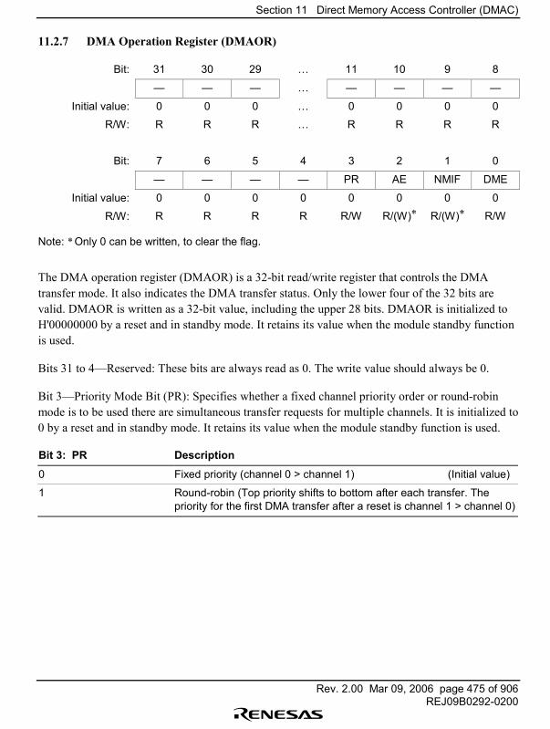
Section 11 Direct Memory Access Controller (DMAC)
Rev. 2.00 Mar 09, 2006 page 475 of 906REJ09B0292-0200
11.2.7 DMA Operation Register (DMAOR)
Bit: 31 30 29 � 11 10 9 8
� � � � � � � �
Initial value: 0 0 0 � 0 0 0 0
R/W: R R R � R R R R
Bit: 7 6 5 4 3 2 1 0
� � � � PR AE NMIF DME
Initial value: 0 0 0 0 0 0 0 0
R/W: R R R R R/W R/(W)* R/(W)* R/W
Note: * Only 0 can be written, to clear the flag.
The DMA operation register (DMAOR) is a 32-bit read/write register that controls the DMAtransfer mode. It also indicates the DMA transfer status. Only the lower four of the 32 bits arevalid. DMAOR is written as a 32-bit value, including the upper 28 bits. DMAOR is initialized toH'00000000 by a reset and in standby mode. It retains its value when the module standby functionis used.
Bits 31 to 4�Reserved: These bits are always read as 0. The write value should always be 0.
Bit 3�Priority Mode Bit (PR): Specifies whether a fixed channel priority order or round-robinmode is to be used there are simultaneous transfer requests for multiple channels. It is initialized to0 by a reset and in standby mode. It retains its value when the module standby function is used.
Bit 3: PR Description
0 Fixed priority (channel 0 > channel 1) (Initial value)
1 Round-robin (Top priority shifts to bottom after each transfer. Thepriority for the first DMA transfer after a reset is channel 1 > channel 0)
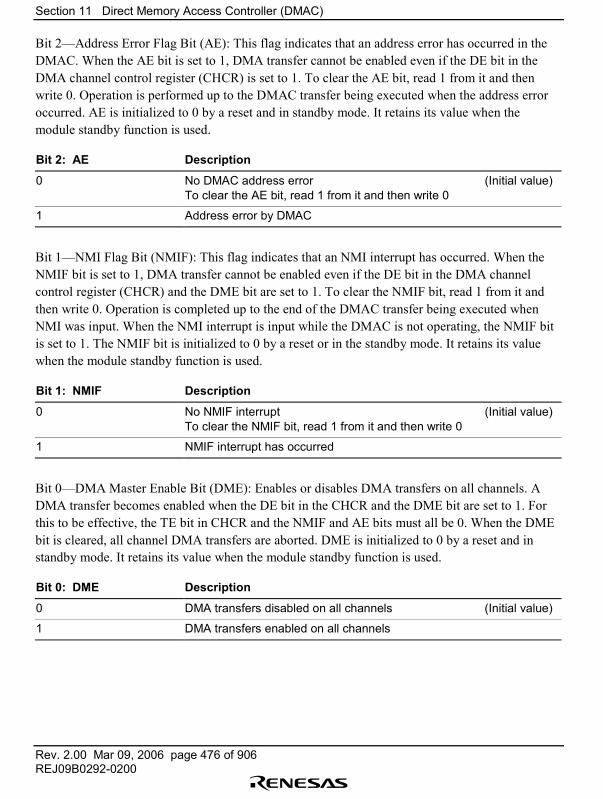
Section 11 Direct Memory Access Controller (DMAC)
Rev. 2.00 Mar 09, 2006 page 476 of 906REJ09B0292-0200
Bit 2�Address Error Flag Bit (AE): This flag indicates that an address error has occurred in theDMAC. When the AE bit is set to 1, DMA transfer cannot be enabled even if the DE bit in theDMA channel control register (CHCR) is set to 1. To clear the AE bit, read 1 from it and thenwrite 0. Operation is performed up to the DMAC transfer being executed when the address erroroccurred. AE is initialized to 0 by a reset and in standby mode. It retains its value when themodule standby function is used.
Bit 2: AE Description
0 No DMAC address error (Initial value)To clear the AE bit, read 1 from it and then write 0
1 Address error by DMAC
Bit 1�NMI Flag Bit (NMIF): This flag indicates that an NMI interrupt has occurred. When theNMIF bit is set to 1, DMA transfer cannot be enabled even if the DE bit in the DMA channelcontrol register (CHCR) and the DME bit are set to 1. To clear the NMIF bit, read 1 from it andthen write 0. Operation is completed up to the end of the DMAC transfer being executed whenNMI was input. When the NMI interrupt is input while the DMAC is not operating, the NMIF bitis set to 1. The NMIF bit is initialized to 0 by a reset or in the standby mode. It retains its valuewhen the module standby function is used.
Bit 1: NMIF Description
0 No NMIF interrupt (Initial value)To clear the NMIF bit, read 1 from it and then write 0
1 NMIF interrupt has occurred
Bit 0�DMA Master Enable Bit (DME): Enables or disables DMA transfers on all channels. ADMA transfer becomes enabled when the DE bit in the CHCR and the DME bit are set to 1. Forthis to be effective, the TE bit in CHCR and the NMIF and AE bits must all be 0. When the DMEbit is cleared, all channel DMA transfers are aborted. DME is initialized to 0 by a reset and instandby mode. It retains its value when the module standby function is used.
Bit 0: DME Description
0 DMA transfers disabled on all channels (Initial value)
1 DMA transfers enabled on all channels
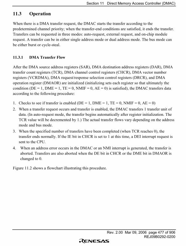
Section 11 Direct Memory Access Controller (DMAC)
Rev. 2.00 Mar 09, 2006 page 477 of 906REJ09B0292-0200
11.3 Operation
When there is a DMA transfer request, the DMAC starts the transfer according to thepredetermined channel priority; when the transfer-end conditions are satisfied, it ends the transfer.Transfers can be requested in three modes: auto-request, external request, and on-chip modulerequest. A transfer can be in either single address mode or dual address mode. The bus mode canbe either burst or cycle-steal.
11.3.1 DMA Transfer Flow
After the DMA source address registers (SAR), DMA destination address registers (DAR), DMAtransfer count registers (TCR), DMA channel control registers (CHCR), DMA vector numberregisters (VCRDMA), DMA request/response selection control registers (DRCR), and DMAoperation register (DMAOR) are initialized (initializing sets each register so that ultimately thecondition (DE = 1, DME = 1, TE = 0, NMIF = 0, AE = 0) is satisfied), the DMAC transfers dataaccording to the following procedure:
1. Checks to see if transfer is enabled (DE = 1, DME = 1, TE = 0, NMIF = 0, AE = 0)2. When a transfer request occurs and transfer is enabled, the DMAC transfers 1 transfer unit of
data. (In auto-request mode, the transfer begins automatically after register initialization. TheTCR value will be decremented by 1.) The actual transfer flows vary depending on the addressmode and bus mode.
3. When the specified number of transfers have been completed (when TCR reaches 0), thetransfer ends normally. If the IE bit in CHCR is set to 1 at this time, a DEI interrupt request issent to the CPU.
4. When an address error occurs in the DMAC or an NMI interrupt is generated, the transfer isaborted. Transfers are also aborted when the DE bit in CHCR or the DME bit in DMAOR ischanged to 0.
Figure 11.2 shows a flowchart illustrating this procedure.
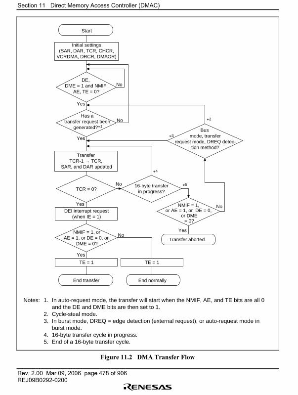
Section 11 Direct Memory Access Controller (DMAC)
Rev. 2.00 Mar 09, 2006 page 478 of 906REJ09B0292-0200
TCR = 0?
DE, DME = 1 and NMIF,
AE, TE = 0?
Has a transfer request been
generated?*1
Transfer aborted
Initial settings(SAR, DAR, TCR, CHCR,
VCRDMA, DRCR, DMAOR)
Transfer TCR-1 → TCR,
SAR, and DAR updated
DEI interrupt request(when IE = 1)
TE = 1 TE = 1
No
Yes
No
Yes
No
Yes
NoYes
No
*3
*5
*4
*2
Start
End normallyEnd transfer
Yes
16-byte transferin progress?
NMIF = 1, orAE = 1, or DE = 0, or
DME = 0?
NMIF = 1, or AE = 1, or DE = 0,
or DME= 0?
Bus mode, transfer
request mode, DREQ detec-tion method?
Notes: 1. In auto-request mode, the transfer will start when the NMIF, AE, and TE bits are all 0 and the DE and DME bits are then set to 1. 2. Cycle-steal mode. 3. In burst mode, DREQ = edge detection (external request), or auto-request mode in burst mode. 4. 16-byte transfer cycle in progress. 5. End of a 16-byte transfer cycle.
Figure 11.2 DMA Transfer Flow

Section 11 Direct Memory Access Controller (DMAC)
Rev. 2.00 Mar 09, 2006 page 479 of 906REJ09B0292-0200
11.3.2 DMA Transfer Requests
DMA transfer requests are usually generated in either the data transfer source or destination, butthey can also be generated by devices that are neither the source nor the destination. Transfers canbe requested in three modes: auto-request, external request, and on-chip peripheral modulerequest. The request mode is selected with the AR bit in DMA channel control registers 0 and 1(CHCR0, CHCR1) and the RS0, RS1, RS2, RS3 and RS4 bits in DMA request/response selectioncontrol registers 0 and 1 (DRCR0, DRCR1).
Table 11.3 Selecting the DMA Transfer Request Using the AR and RS Bits
CHCR DRCR
AR RS4 RS3 RS2 RS1 RS0 Request Mode Resource Selection
0 0 0 0 0 0 Module request mode DREQ (external request)
1 0 1 SCIF channel 1 RXI
1 0 SCIF channel 1 TXI
1 0 0 1 SCIF channel 2 RXI
1 0 SCIF channel 2 TXI
1 0 TPU TGI0A
1 TPU TGI0B
1 0 TPU TGI0C
1 TPU TGI0D
1 0 0 0 SIOF RDFI
1 0 SIOF TDEI
1 0 1 SIO channel 1 RDFI
1 0 SIO channel 1 TDEI
1 0 0 1 SIO channel 2 RDFI
1 0 SIO channel 2 TDEI
1 * * * * * Auto-request modeNote: * Don�t care
Auto-Request Mode: When there is no transfer request signal from an external source (as in amemory-to-memory transfer, the auto-request mode allows the DMAC to automatically generate atransfer request signal internally. When the DE bits in CHCR0 and CHCR1 and the DME bit inthe DMA operation register (DMAOR) are set to 1, the transfer begins (so long as the TE bits inCHCR0 and CHCR1 and the NMIF and AE bits in DMAOR are all 0).
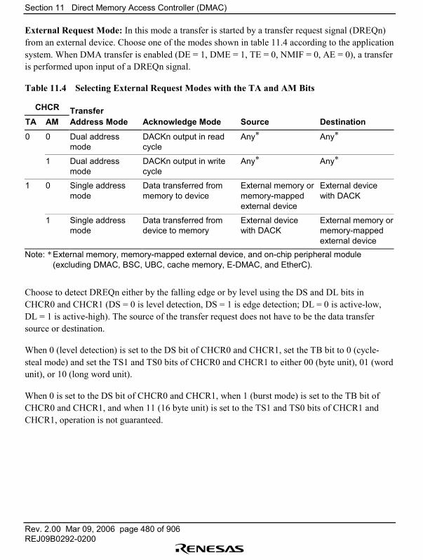
Section 11 Direct Memory Access Controller (DMAC)
Rev. 2.00 Mar 09, 2006 page 480 of 906REJ09B0292-0200
External Request Mode: In this mode a transfer is started by a transfer request signal (DREQn)from an external device. Choose one of the modes shown in table 11.4 according to the applicationsystem. When DMA transfer is enabled (DE = 1, DME = 1, TE = 0, NMIF = 0, AE = 0), a transferis performed upon input of a DREQn signal.
Table 11.4 Selecting External Request Modes with the TA and AM Bits
CHCR TransferTA AM Address Mode Acknowledge Mode Source Destination
0 0 Dual addressmode
DACKn output in readcycle
Any* Any*
1 Dual addressmode
DACKn output in writecycle
Any* Any*
1 0 Single addressmode
Data transferred frommemory to device
External memory ormemory-mappedexternal device
External devicewith DACK
1 Single addressmode
Data transferred fromdevice to memory
External devicewith DACK
External memory ormemory-mappedexternal device
Note: * External memory, memory-mapped external device, and on-chip peripheral module(excluding DMAC, BSC, UBC, cache memory, E-DMAC, and EtherC).
Choose to detect DREQn either by the falling edge or by level using the DS and DL bits inCHCR0 and CHCR1 (DS = 0 is level detection, DS = 1 is edge detection; DL = 0 is active-low,DL = 1 is active-high). The source of the transfer request does not have to be the data transfersource or destination.
When 0 (level detection) is set to the DS bit of CHCR0 and CHCR1, set the TB bit to 0 (cycle-steal mode) and set the TS1 and TS0 bits of CHCR0 and CHCR1 to either 00 (byte unit), 01 (wordunit), or 10 (long word unit).
When 0 is set to the DS bit of CHCR0 and CHCR1, when 1 (burst mode) is set to the TB bit ofCHCR0 and CHCR1, and when 11 (16 byte unit) is set to the TS1 and TS0 bits of CHCR1 andCHCR1, operation is not guaranteed.
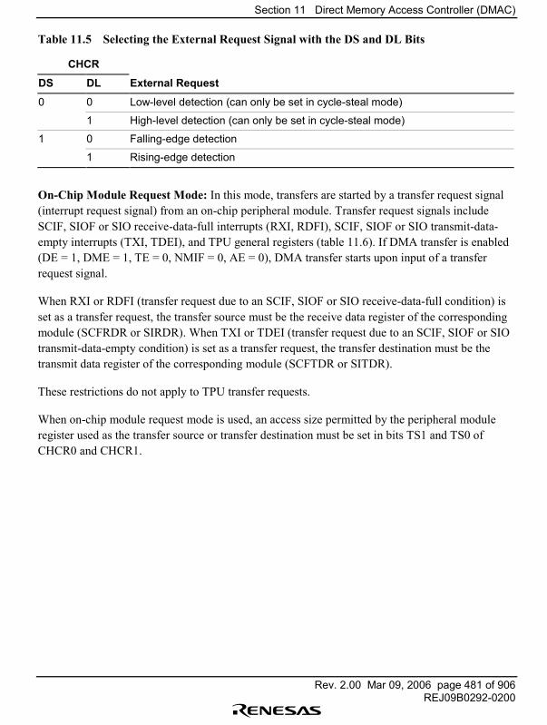
Section 11 Direct Memory Access Controller (DMAC)
Rev. 2.00 Mar 09, 2006 page 481 of 906REJ09B0292-0200
Table 11.5 Selecting the External Request Signal with the DS and DL Bits
CHCR
DS DL External Request
0 0 Low-level detection (can only be set in cycle-steal mode)
1 High-level detection (can only be set in cycle-steal mode)
1 0 Falling-edge detection
1 Rising-edge detection
On-Chip Module Request Mode: In this mode, transfers are started by a transfer request signal(interrupt request signal) from an on-chip peripheral module. Transfer request signals includeSCIF, SIOF or SIO receive-data-full interrupts (RXI, RDFI), SCIF, SIOF or SIO transmit-data-empty interrupts (TXI, TDEI), and TPU general registers (table 11.6). If DMA transfer is enabled(DE = 1, DME = 1, TE = 0, NMIF = 0, AE = 0), DMA transfer starts upon input of a transferrequest signal.
When RXI or RDFI (transfer request due to an SCIF, SIOF or SIO receive-data-full condition) isset as a transfer request, the transfer source must be the receive data register of the correspondingmodule (SCFRDR or SIRDR). When TXI or TDEI (transfer request due to an SCIF, SIOF or SIOtransmit-data-empty condition) is set as a transfer request, the transfer destination must be thetransmit data register of the corresponding module (SCFTDR or SITDR).
These restrictions do not apply to TPU transfer requests.
When on-chip module request mode is used, an access size permitted by the peripheral moduleregister used as the transfer source or transfer destination must be set in bits TS1 and TS0 ofCHCR0 and CHCR1.
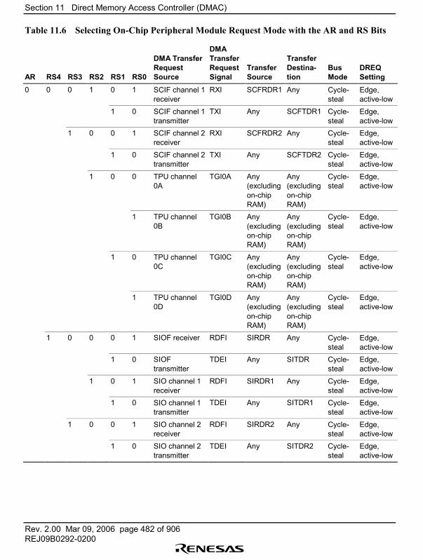
Section 11 Direct Memory Access Controller (DMAC)
Rev. 2.00 Mar 09, 2006 page 482 of 906REJ09B0292-0200
Table 11.6 Selecting On-Chip Peripheral Module Request Mode with the AR and RS Bits
AR RS4 RS3 RS2 RS1 RS0
DMA TransferRequestSource
DMATransferRequestSignal
TransferSource
TransferDestina-tion
BusMode
DREQSetting
0 0 0 1 0 1 SCIF channel 1receiver
RXI SCFRDR1 Any Cycle-steal
Edge,active-low
1 0 SCIF channel 1transmitter
TXI Any SCFTDR1 Cycle-steal
Edge,active-low
1 0 0 1 SCIF channel 2receiver
RXI SCFRDR2 Any Cycle-steal
Edge,active-low
1 0 SCIF channel 2transmitter
TXI Any SCFTDR2 Cycle-steal
Edge,active-low
1 0 0 TPU channel0A
TGI0A Any(excludingon-chipRAM)
Any(excludingon-chipRAM)
Cycle-steal
Edge,active-low
1 TPU channel0B
TGI0B Any(excludingon-chipRAM)
Any(excludingon-chipRAM)
Cycle-steal
Edge,active-low
1 0 TPU channel0C
TGI0C Any(excludingon-chipRAM)
Any(excludingon-chipRAM)
Cycle-steal
Edge,active-low
1 TPU channel0D
TGI0D Any(excludingon-chipRAM)
Any(excludingon-chipRAM)
Cycle-steal
Edge,active-low
1 0 0 0 1 SIOF receiver RDFI SIRDR Any Cycle-steal
Edge,active-low
1 0 SIOFtransmitter
TDEI Any SITDR Cycle-steal
Edge,active-low
1 0 1 SIO channel 1receiver
RDFI SIRDR1 Any Cycle-steal
Edge,active-low
1 0 SIO channel 1transmitter
TDEI Any SITDR1 Cycle-steal
Edge,active-low
1 0 0 1 SIO channel 2receiver
RDFI SIRDR2 Any Cycle-steal
Edge,active-low
1 0 SIO channel 2transmitter
TDEI Any SITDR2 Cycle-steal
Edge,active-low
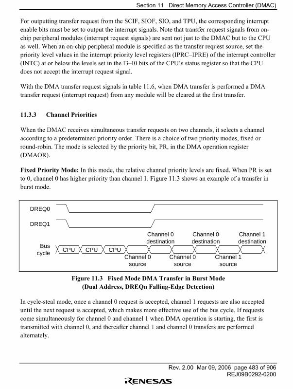
Section 11 Direct Memory Access Controller (DMAC)
Rev. 2.00 Mar 09, 2006 page 483 of 906REJ09B0292-0200
For outputting transfer request from the SCIF, SIOF, SIO, and TPU, the corresponding interruptenable bits must be set to output the interrupt signals. Note that transfer request signals from on-chip peripheral modules (interrupt request signals) are sent not just to the DMAC but to the CPUas well. When an on-chip peripheral module is specified as the transfer request source, set thepriority level values in the interrupt priority level registers (IPRC�IPRE) of the interrupt controller(INTC) at or below the levels set in the I3�I0 bits of the CPU�s status register so that the CPUdoes not accept the interrupt request signal.
With the DMA transfer request signals in table 11.6, when DMA transfer is performed a DMAtransfer request (interrupt request) from any module will be cleared at the first transfer.
11.3.3 Channel Priorities
When the DMAC receives simultaneous transfer requests on two channels, it selects a channelaccording to a predetermined priority order. There is a choice of two priority modes, fixed orround-robin. The mode is selected by the priority bit, PR, in the DMA operation register(DMAOR).
Fixed Priority Mode: In this mode, the relative channel priority levels are fixed. When PR is setto 0, channel 0 has higher priority than channel 1. Figure 11.3 shows an example of a transfer inburst mode.
CPUBus
cycle
DREQ1
DREQ0
CPU CPUChannel 0
source
Channel 0destination
Channel 0source
Channel 0destination
Channel 1source
Channel 1destination
Figure 11.3 Fixed Mode DMA Transfer in Burst Mode(Dual Address, DREQn Falling-Edge Detection)
In cycle-steal mode, once a channel 0 request is accepted, channel 1 requests are also accepteduntil the next request is accepted, which makes more effective use of the bus cycle. If requestscome simultaneously for channel 0 and channel 1 when DMA operation is starting, the first istransmitted with channel 0, and thereafter channel 1 and channel 0 transfers are performedalternately.
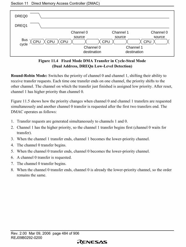
Section 11 Direct Memory Access Controller (DMAC)
Rev. 2.00 Mar 09, 2006 page 484 of 906REJ09B0292-0200
CPUBuscycle
DREQ1
DREQ0
CPU CPU CPUCPU
Channel 0source
Channel 1source
Channel 0source
Channel 0destination
Channel 1destination
Figure 11.4 Fixed Mode DMA Transfer in Cycle-Steal Mode(Dual Address, DREQn Low-Level Detection)
Round-Robin Mode: Switches the priority of channel 0 and channel 1, shifting their ability toreceive transfer requests. Each time one transfer ends on one channel, the priority shifts to theother channel. The channel on which the transfer just finished is assigned low priority. After reset,channel 1 has higher priority than channel 0.
Figure 11.5 shows how the priority changes when channel 0 and channel 1 transfers are requestedsimultaneously and another channel 0 transfer is requested after the first two transfers end. TheDMAC operates as follows:
1. Transfer requests are generated simultaneously to channels 1 and 0.2. Channel 1 has the higher priority, so the channel 1 transfer begins first (channel 0 waits for
transfer).3. When the channel 1 transfer ends, channel 1 becomes the lower-priority channel.4. The channel 0 transfer begins.5. When the channel 0 transfer ends, channel 0 becomes the lower-priority channel.6. A channel 0 transfer is requested.7. The channel 0 transfer begins.8. When the channel 0 transfer ends, channel 0 is already the lower-priority channel, so the order
remains the same.
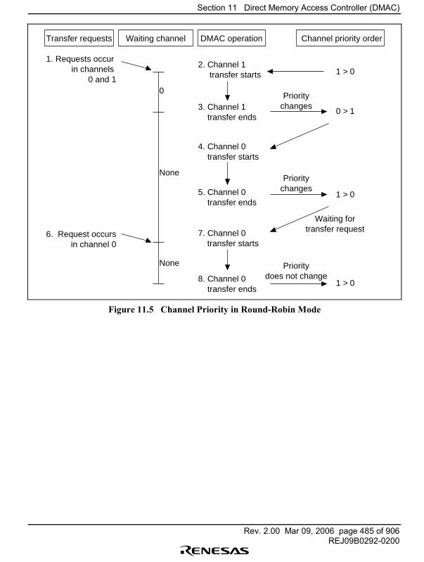
Section 11 Direct Memory Access Controller (DMAC)
Rev. 2.00 Mar 09, 2006 page 485 of 906REJ09B0292-0200
0
None
None
1. Requests occur in channels
0 and 1
6. Request occursin channel 0
2. Channel 1 transfer starts
3. Channel 1 transfer ends
5. Channel 0 transfer ends
7. Channel 0 transfer starts
4. Channel 0 transfer starts
8. Channel 0 transfer ends
Prioritychanges
1 > 0
0 > 1
1 > 0
1 > 0
Transfer requests Waiting channel DMAC operation Channel priority order
Prioritychanges
Prioritydoes not change
Waiting fortransfer request
Figure 11.5 Channel Priority in Round-Robin Mode
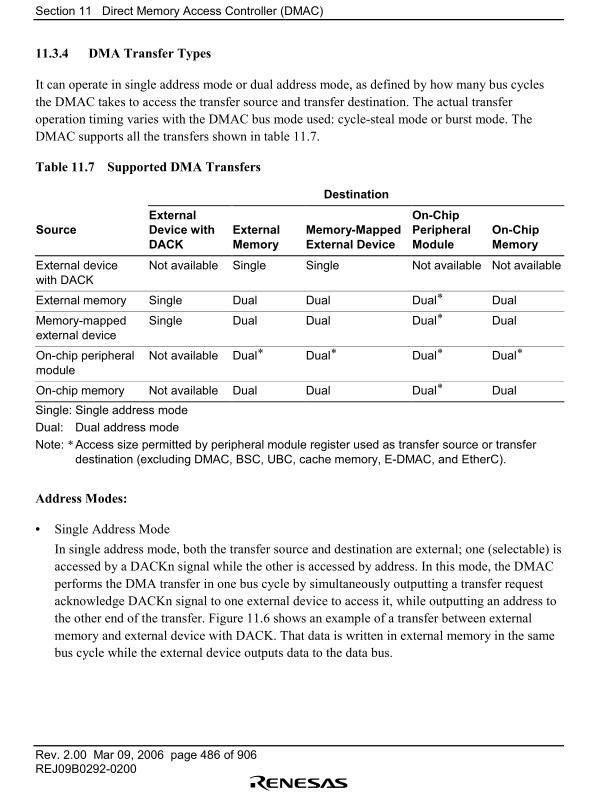
Section 11 Direct Memory Access Controller (DMAC)
Rev. 2.00 Mar 09, 2006 page 486 of 906REJ09B0292-0200
11.3.4 DMA Transfer Types
It can operate in single address mode or dual address mode, as defined by how many bus cyclesthe DMAC takes to access the transfer source and transfer destination. The actual transferoperation timing varies with the DMAC bus mode used: cycle-steal mode or burst mode. TheDMAC supports all the transfers shown in table 11.7.
Table 11.7 Supported DMA Transfers
Destination
SourceExternalDevice withDACK
ExternalMemory
Memory-MappedExternal Device
On-ChipPeripheralModule
On-ChipMemory
External devicewith DACK
Not available Single Single Not available Not available
External memory Single Dual Dual Dual* Dual
Memory-mappedexternal device
Single Dual Dual Dual* Dual
On-chip peripheralmodule
Not available Dual* Dual* Dual* Dual*
On-chip memory Not available Dual Dual Dual* DualSingle: Single address modeDual: Dual address modeNote: * Access size permitted by peripheral module register used as transfer source or transfer
destination (excluding DMAC, BSC, UBC, cache memory, E-DMAC, and EtherC).
Address Modes:
• Single Address ModeIn single address mode, both the transfer source and destination are external; one (selectable) isaccessed by a DACKn signal while the other is accessed by address. In this mode, the DMACperforms the DMA transfer in one bus cycle by simultaneously outputting a transfer requestacknowledge DACKn signal to one external device to access it, while outputting an address tothe other end of the transfer. Figure 11.6 shows an example of a transfer between externalmemory and external device with DACK. That data is written in external memory in the samebus cycle while the external device outputs data to the data bus.
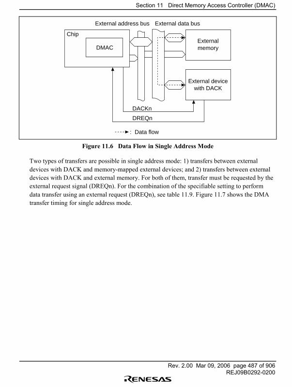
Section 11 Direct Memory Access Controller (DMAC)
Rev. 2.00 Mar 09, 2006 page 487 of 906REJ09B0292-0200
DMAC
DACKn
DREQn
Externalmemory
External devicewith DACK
Chip
External address bus
: Data flow
External data bus
Figure 11.6 Data Flow in Single Address Mode
Two types of transfers are possible in single address mode: 1) transfers between externaldevices with DACK and memory-mapped external devices; and 2) transfers between externaldevices with DACK and external memory. For both of them, transfer must be requested by theexternal request signal (DREQn). For the combination of the specifiable setting to performdata transfer using an external request (DREQn), see table 11.9. Figure 11.7 shows the DMAtransfer timing for single address mode.
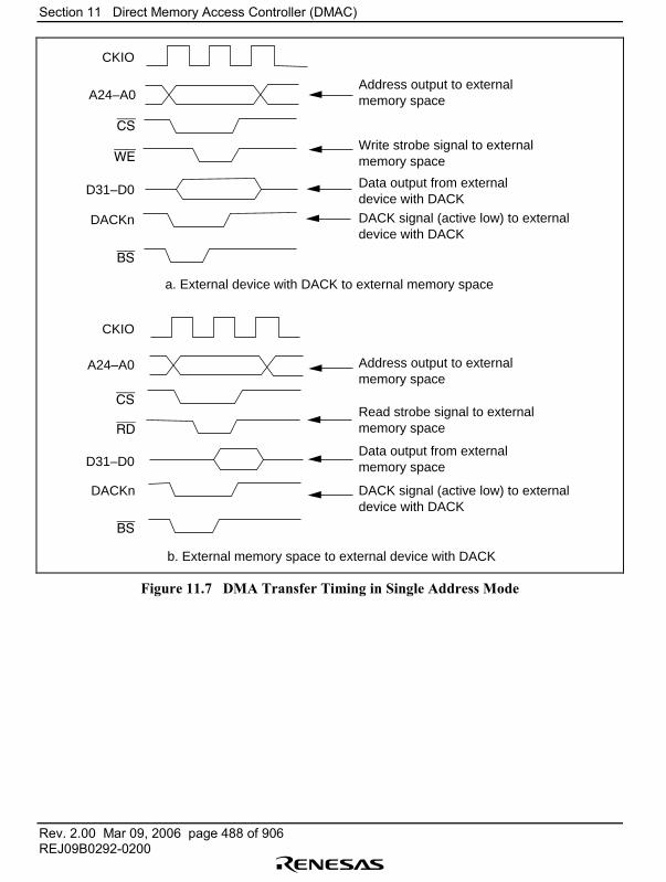
Section 11 Direct Memory Access Controller (DMAC)
Rev. 2.00 Mar 09, 2006 page 488 of 906REJ09B0292-0200
CKIO
A24–A0
CS
D31–D0
DACKn
BS
CKIO
A24–A0
CS
D31–D0
BS
DACKn
WE
RD
Address output to external memory space
Write strobe signal to externalmemory space
Data output from externaldevice with DACKDACK signal (active low) to external device with DACK
a. External device with DACK to external memory space
Address output to external memory space
Data output from external memory space
Read strobe signal to externalmemory space
DACK signal (active low) to external device with DACK
b. External memory space to external device with DACK
Figure 11.7 DMA Transfer Timing in Single Address Mode
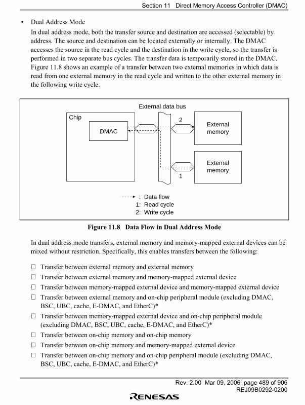
Section 11 Direct Memory Access Controller (DMAC)
Rev. 2.00 Mar 09, 2006 page 489 of 906REJ09B0292-0200
• Dual Address ModeIn dual address mode, both the transfer source and destination are accessed (selectable) byaddress. The source and destination can be located externally or internally. The DMACaccesses the source in the read cycle and the destination in the write cycle, so the transfer isperformed in two separate bus cycles. The transfer data is temporarily stored in the DMAC.Figure 11.8 shows an example of a transfer between two external memories in which data isread from one external memory in the read cycle and written to the other external memory inthe following write cycle.
DMACExternalmemory
Externalmemory
Chip 2
1
External data bus
: Data flow1: Read cycle2: Write cycle
Figure 11.8 Data Flow in Dual Address Mode
In dual address mode transfers, external memory and memory-mapped external devices can bemixed without restriction. Specifically, this enables transfers between the following:
Transfer between external memory and external memory Transfer between external memory and memory-mapped external device Transfer between memory-mapped external device and memory-mapped external device Transfer between external memory and on-chip peripheral module (excluding DMAC,
BSC, UBC, cache, E-DMAC, and EtherC)* Transfer between memory-mapped external device and on-chip peripheral module
(excluding DMAC, BSC, UBC, cache, E-DMAC, and EtherC)* Transfer between on-chip memory and on-chip memory Transfer between on-chip memory and memory-mapped external device Transfer between on-chip memory and on-chip peripheral module (excluding DMAC,
BSC, UBC, cache, E-DMAC, and EtherC)*
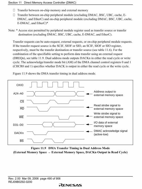
Section 11 Direct Memory Access Controller (DMAC)
Rev. 2.00 Mar 09, 2006 page 490 of 906REJ09B0292-0200
Transfer between on-chip memory and external memory Transfer between on-chip peripheral module (excluding DMAC, BSC, UBC, cache, E-
DMAC, and EtherC) and on-chip peripheral module (excluding DMAC, BSC, UBC, cache,E-DMAC, and EtherC)*
Note: * Access size permitted by peripheral module register used as transfer source or transferdestination (excluding DMAC, BSC, UBC, cache, E-DMAC, and EtherC).
Transfer requests can be auto-request, external requests, or on-chip peripheral module requests.If the transfer request source is the SCIF, SIOF or SIO, an SCIF, SIOF or SIO register,respectively, must be the transfer destination or transfer source (see table 11.6). For thecombination of the specifiable setting to perform data transfer using an external request(DREQn), see table 11.9. Dual address mode outputs DACKn in either the read cycle or writecycle. The acknowledge/transfer mode bit (AM) of the DMA channel control registers 0 and 1(CHCR0 and 1) specifies whether DACK is output in either the read cycle or the write cycle.
Figure 11.9 shows the DMA transfer timing in dual address mode.
CKIO
A24–A0
CS
D31–D0
DACKn
RD
WE
BS
Address output toexternal memory space
Read strobe signal toexternal memory space
Write strobe signal toexternal memory space
I/O data of externalmemory space
DMAC acknowledge signal(active-low)
Figure 11.9 DMA Transfer Timing in Dual Address Mode(External Memory Space → External Memory Space, DACKn Output in Read Cycle)
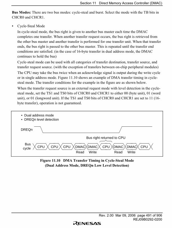
Section 11 Direct Memory Access Controller (DMAC)
Rev. 2.00 Mar 09, 2006 page 491 of 906REJ09B0292-0200
Bus Modes: There are two bus modes: cycle-steal and burst. Select the mode with the TB bits inCHCR0 and CHCR1.
• Cycle-Steal ModeIn cycle-steal mode, the bus right is given to another bus master each time the DMACcompletes one transfer. When another transfer request occurs, the bus right is retrieved fromthe other bus master and another transfer is performed for one transfer unit. When that transferends, the bus right is passed to the other bus master. This is repeated until the transfer endconditions are satisfied. (in the case of 16-byte transfer in dual address mode, the DMACcontinues to hold the bus)Cycle-steal mode can be used with all categories of transfer destination, transfer source, andtransfer request source. (with the exception of transfers between on-chip peripheral modules)The CPU may take the bus twice when an acknowledge signal is output during the write cycleor in single address mode. Figure 11.10 shows an example of DMA transfer timing in cycle-steal mode. The transfer conditions for the example in the figure are as shown below.When the transfer request source is an external request mode with level detection in the cycle-steal mode, set the TS1 and TS0 bits of CHCR0 and CHCR1 to either 00 (byte unit), 01 (wordunit), or 01 (longword unit). If the TS1 and TS0 bits of CHCR0 and CHCR1 are set to 11 (16-byte transfer), operation is not guaranteed.
CPU CPU CPU DMAC DMAC CPU DMAC DMAC CPU
DREQn
• Dual address mode• DREQn level detection
Buscycle
Bus right returned to CPU
Read Write Read Write
Figure 11.10 DMA Transfer Timing in Cycle-Steal Mode(Dual Address Mode, DREQn Low Level Detection)
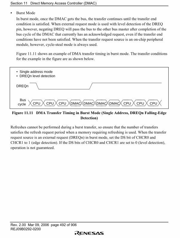
Section 11 Direct Memory Access Controller (DMAC)
Rev. 2.00 Mar 09, 2006 page 492 of 906REJ09B0292-0200
• Burst ModeIn burst mode, once the DMAC gets the bus, the transfer continues until the transfer endcondition is satisfied. When external request mode is used with level detection of the DREQpin, however, negating DREQ will pass the bus to the other bus master after completion of thebus cycle of the DMAC that currently has an acknowledged request, even if the transfer endconditions have not been satisfied. When the transfer request source is an on-chip peripheralmodule, however, cycle-steal mode is always used.
Figure 11.11 shows an example of DMA transfer timing in burst mode. The transfer conditionsfor the example in the figure are as shown below.
CPU CPU CPU DMAC DMAC DMAC DMAC CPU
DREQn
• Single address mode• DREQn level detection
Buscycle CPU CPU
Figure 11.11 DMA Transfer Timing in Burst Mode (Single Address, DREQn Falling-EdgeDetection)
Refreshes cannot be performed during a burst transfer, so ensure that the number of transferssatisfies the refresh request period when a memory requiring refreshing is used. When the transferrequest source is an external request (DREQn) in burst mode, set the DS bit of CHCR0 andCHCR1 to 1 (edge detection). If the DS bits of CHCR0 and CHCR1 are set to 0 (level detection),operation is not guaranteed.
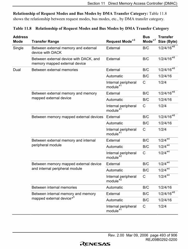
Section 11 Direct Memory Access Controller (DMAC)
Rev. 2.00 Mar 09, 2006 page 493 of 906REJ09B0292-0200
Relationship of Request Modes and Bus Modes by DMA Transfer Category: Table 11.8shows the relationship between request modes, bus modes, etc., by DMA transfer category.
Table 11.8 Relationship of Request Modes and Bus Modes by DMA Transfer Category
AddressMode Transfer Range Request Mode*3
BusMode*7
TransferSize (Byte)
Single Between external memory and externaldevice with DACK
External B/C 1/2/4/16*8
Between external device with DACK, andmemory mapped external device
External B/C 1/2/4/16*8
Dual Between external memories External B/C 1/2/4/16*8
Automatic B/C 1/2/4/16
Internal peripheralmodule*1
C 1/2/4
Between external memory and memory External B/C 1/2/4/16*8
mapped external device Automatic B/C 1/2/4/16
Internal peripheralmodule*1
C 1/2/4
Between memory mapped external devices External B/C 1/2/4/16*8
Automatic B/C 1/2/4/16
Internal peripheralmodule*1
C 1/2/4
Between external memory and internal External B/C 1/2/4*4
peripheral module Automatic B/C 1/2/4*4
Internal peripheralmodule*2
C 1/2/4*4
Between memory mapped external device External B/C 1/2/4*4
and internal peripheral module Automatic B/C 1/2/4*4
Internal peripheralmodule*2
C 1/2/4*4
Between internal memories Automatic B/C 1/2/4/16
Between internal memory and memory External B/C 1/2/4/16*8
mapped external device*5Automatic B/C 1/2/4/16
Internal peripheralmodule*1
C 1/2/4
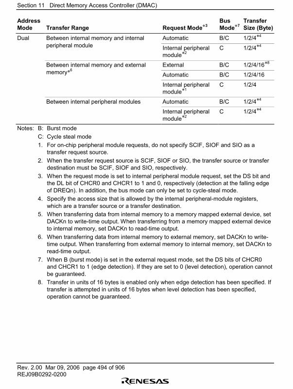
Section 11 Direct Memory Access Controller (DMAC)
Rev. 2.00 Mar 09, 2006 page 494 of 906REJ09B0292-0200
AddressMode Transfer Range Request Mode*3
BusMode*7
TransferSize (Byte)
Dual Between internal memory and internal Automatic B/C 1/2/4*4
peripheral module Internal peripheralmodule*2
C 1/2/4*4
Between internal memory and external External B/C 1/2/4/16*8
memory*6Automatic B/C 1/2/4/16
Internal peripheralmodule*1
C 1/2/4
Between internal peripheral modules Automatic B/C 1/2/4*4
Internal peripheralmodule*2
C 1/2/4*4
Notes: B: Burst modeC: Cycle steal mode1. For on-chip peripheral module requests, do not specify SCIF, SIOF and SIO as a
transfer request source.2. When the transfer request source is SCIF, SIOF or SIO, the transfer source or transfer
destination must be SCIF, SIOF and SIO, respectively.3. When the request mode is set to internal peripheral module request, set the DS bit and
the DL bit of CHCR0 and CHCR1 to 1 and 0, respectively (detection at the falling edgeof DREQn). In addition, the bus mode can only be set to cycle-steal mode.
4. Specify the access size that is allowed by the internal peripheral-module registers,which are a transfer source or a transfer destination.
5. When transferring data from internal memory to a memory mapped external device, setDACKn to write-time output. When transferring from a memory mapped external deviceto internal memory, set DACKn to read-time output.
6. When transferring data from internal memory to external memory, set DACKn to write-time output. When transferring from external memory to internal memory, set DACKn toread-time output.
7. When B (burst mode) is set in the external request mode, set the DS bits of CHCR0and CHCR1 to 1 (edge detection). If they are set to 0 (level detection), operation cannotbe guaranteed.
8. Transfer in units of 16 bytes is enabled only when edge detection has been specified. Iftransfer is attempted in units of 16 bytes when level detection has been specified,operation cannot be guaranteed.
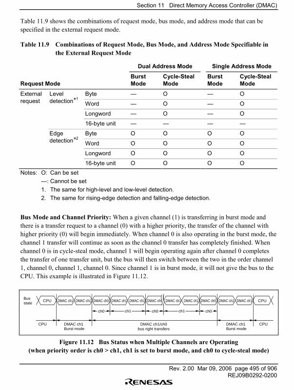
Section 11 Direct Memory Access Controller (DMAC)
Rev. 2.00 Mar 09, 2006 page 495 of 906REJ09B0292-0200
Table 11.9 shows the combinations of request mode, bus mode, and address mode that can bespecified in the external request mode.
Table 11.9 Combinations of Request Mode, Bus Mode, and Address Mode Specifiable inthe External Request Mode
Dual Address Mode Single Address Mode
Request ModeBurstMode
Cycle-StealMode
BurstMode
Cycle-StealMode
Byte � O � OExternalrequest
Leveldetection*1
Word � O � O
Longword � O � O
16-byte unit � � � �
Byte O O O OEdgedetection*2
Word O O O O
Longword O O O O
16-byte unit O O O ONotes: O: Can be set
�: Cannot be set1. The same for high-level and low-level detection.2. The same for rising-edge detection and falling-edge detection.
Bus Mode and Channel Priority: When a given channel (1) is transferring in burst mode andthere is a transfer request to a channel (0) with a higher priority, the transfer of the channel withhigher priority (0) will begin immediately. When channel 0 is also operating in the burst mode, thechannel 1 transfer will continue as soon as the channel 0 transfer has completely finished. Whenchannel 0 is in cycle-steal mode, channel 1 will begin operating again after channel 0 completesthe transfer of one transfer unit, but the bus will then switch between the two in the order channel1, channel 0, channel 1, channel 0. Since channel 1 is in burst mode, it will not give the bus to theCPU. This example is illustrated in Figure 11.12.
Busstate
CPUDMAC ch1 DMAC ch1 DMAC ch0 DMAC ch0DMAC ch1 DMAC ch1 DMAC ch1 DMAC ch1 DMAC ch0 DMAC ch1 DMAC ch1CPU
ch1ch0 ch0 ch1 ch0
CPU DMAC ch1Burst mode
DMAC ch1Burst mode
DMAC ch1/ch0bus right transfers
CPU
Figure 11.12 Bus Status when Multiple Channels are Operating(when priority order is ch0 > ch1, ch1 is set to burst mode, and ch0 to cycle-steal mode)
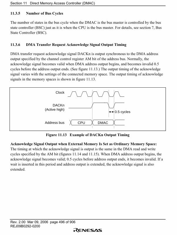
Section 11 Direct Memory Access Controller (DMAC)
Rev. 2.00 Mar 09, 2006 page 496 of 906REJ09B0292-0200
11.3.5 Number of Bus Cycles
The number of states in the bus cycle when the DMAC is the bus master is controlled by the busstate controller (BSC) just as it is when the CPU is the bus master. For details, see section 7, BusState Controller (BSC).
11.3.6 DMA Transfer Request Acknowledge Signal Output Timing
DMA transfer request acknowledge signal DACKn is output synchronous to the DMA addressoutput specified by the channel control register AM bit of the address bus. Normally, theacknowledge signal becomes valid when DMA address output begins, and becomes invalid 0.5cycles before the address output ends. (See figure 11.13.) The output timing of the acknowledgesignal varies with the settings of the connected memory space. The output timing of acknowledgesignals in the memory spaces is shown in figure 11.13.
Clock
DACKn(Active high)
Address bus CPU DMAC
0.5 cycles
Figure 11.13 Example of DACKn Output Timing
Acknowledge Signal Output when External Memory Is Set as Ordinary Memory Space:The timing at which the acknowledge signal is output is the same in the DMA read and writecycles specified by the AM bit (figures 11.14 and 11.15). When DMA address output begins, theacknowledge signal becomes valid; 0.5 cycles before address output ends, it becomes invalid. If await is inserted in this period and address output is extended, the acknowledge signal is alsoextended.
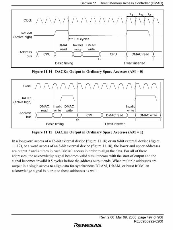
Section 11 Direct Memory Access Controller (DMAC)
Rev. 2.00 Mar 09, 2006 page 497 of 906REJ09B0292-0200
Clock
DACKn(Active high)
Addressbus
CPU
DMACread
DMACwrite
Invalidwrite
CPU
0.5 cycles
DMAC read
T1 TW T2
Basic timing 1 wait inserted
Figure 11.14 DACKn Output in Ordinary Space Accesses (AM = 0)
Clock
DACKn(Active high)
Addressbus
DMACread
DMACwrite
Invalidwrite
Invalidwrite
CPU DMAC read
Basic timing 1 wait inserted
DMAC write
Figure 11.15 DACKn Output in Ordinary Space Accesses (AM = 1)
In a longword access of a 16-bit external device (figure 11.16) or an 8-bit external device (figure11.17), or a word access of an 8-bit external device (figure 11.18), the lower and upper addressesare output 2 and 4 times in each DMAC access in order to align the data. For all of theseaddresses, the acknowledge signal becomes valid simultaneous with the start of output and thesignal becomes invalid 0.5 cycles before the address output ends. When multiple addresses areoutput in a single access to align data for synchronous DRAM, DRAM, or burst ROM, anacknowledge signal is output to those addresses as well.
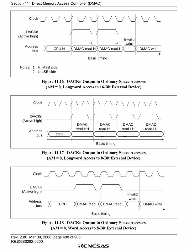
Section 11 Direct Memory Access Controller (DMAC)
Rev. 2.00 Mar 09, 2006 page 498 of 906REJ09B0292-0200
Clock
DACKn(Active high)
Addressbus
CPU H DMAC read H DMAC read L
Invalidwrite
DMAC write
Basic timing
*1 *2
Notes: 1. H: MSB side 2. L: LSB side
Figure 11.16 DACKn Output in Ordinary Space Accesses(AM = 0, Longword Access to 16-Bit External Device)
Clock
DACKn(Active high)
Addressbus CPU
DMACread HH
DMACread HL
DMACread LH
DMACread LL
Basic timing
Figure 11.17 DACKn Output in Ordinary Space Accesses(AM = 0, Longword Access to 8-Bit External Device)
Clock
DACKn(Active high)
Addressbus CPU DMAC read H DMAC read L
Invalidwrite
DMAC write
Basic timing
Figure 11.18 DACKn Output in Ordinary Space Accesses(AM = 0, Word Access to 8-Bit External Device)
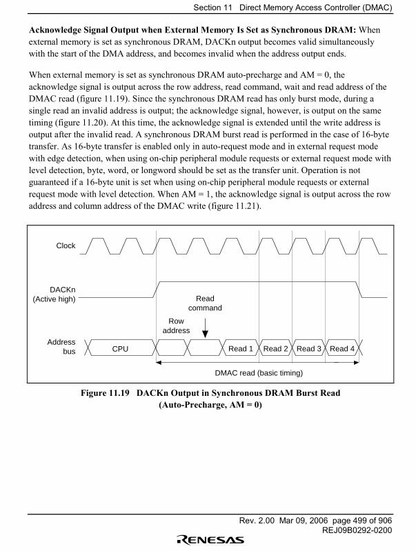
Section 11 Direct Memory Access Controller (DMAC)
Rev. 2.00 Mar 09, 2006 page 499 of 906REJ09B0292-0200
Acknowledge Signal Output when External Memory Is Set as Synchronous DRAM: Whenexternal memory is set as synchronous DRAM, DACKn output becomes valid simultaneouslywith the start of the DMA address, and becomes invalid when the address output ends.
When external memory is set as synchronous DRAM auto-precharge and AM = 0, theacknowledge signal is output across the row address, read command, wait and read address of theDMAC read (figure 11.19). Since the synchronous DRAM read has only burst mode, during asingle read an invalid address is output; the acknowledge signal, however, is output on the sametiming (figure 11.20). At this time, the acknowledge signal is extended until the write address isoutput after the invalid read. A synchronous DRAM burst read is performed in the case of 16-bytetransfer. As 16-byte transfer is enabled only in auto-request mode and in external request modewith edge detection, when using on-chip peripheral module requests or external request mode withlevel detection, byte, word, or longword should be set as the transfer unit. Operation is notguaranteed if a 16-byte unit is set when using on-chip peripheral module requests or externalrequest mode with level detection. When AM = 1, the acknowledge signal is output across the rowaddress and column address of the DMAC write (figure 11.21).
Clock
DACKn(Active high)
Addressbus CPU
DMAC read (basic timing)
Rowaddress
Read 1 Read 2 Read 3 Read 4
Readcommand
Figure 11.19 DACKn Output in Synchronous DRAM Burst Read(Auto-Precharge, AM = 0)
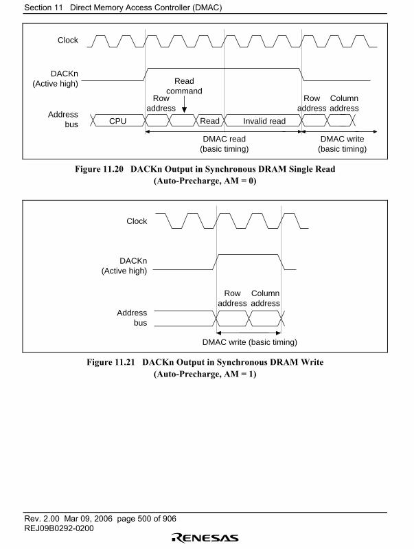
Section 11 Direct Memory Access Controller (DMAC)
Rev. 2.00 Mar 09, 2006 page 500 of 906REJ09B0292-0200
Clock
DACKn(Active high)
Addressbus CPU Invalid read
DMAC read(basic timing)
DMAC write(basic timing)
Rowaddress
Columnaddress
Rowaddress
Read
Readcommand
Figure 11.20 DACKn Output in Synchronous DRAM Single Read(Auto-Precharge, AM = 0)
Clock
DACKn(Active high)
Addressbus
DMAC write (basic timing)
Columnaddress
Rowaddress
Figure 11.21 DACKn Output in Synchronous DRAM Write(Auto-Precharge, AM = 1)
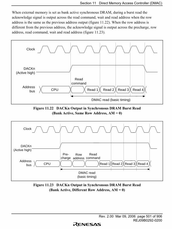
Section 11 Direct Memory Access Controller (DMAC)
Rev. 2.00 Mar 09, 2006 page 501 of 906REJ09B0292-0200
When external memory is set as bank active synchronous DRAM, during a burst read theacknowledge signal is output across the read command, wait and read address when the rowaddress is the same as the previous address output (figure 11.22). When the row address isdifferent from the previous address, the acknowledge signal is output across the precharge, rowaddress, read command, wait and read address (figure 11.23).
Clock
DACKn(Active high)
Addressbus CPU
DMAC read (basic timing)
Readcommand
Read 1 Read 2 Read 3 Read 4
Figure 11.22 DACKn Output in Synchronous DRAM Burst Read(Bank Active, Same Row Address, AM = 0)
Clock
DACKn(Active high)
Addressbus CPU
DMAC read(basic timing)
Pre-charge
Readcommand
Read 1 Read 2 Read 3 Read 4
Rowaddress
Figure 11.23 DACKn Output in Synchronous DRAM Burst Read(Bank Active, Different Row Address, AM = 0)
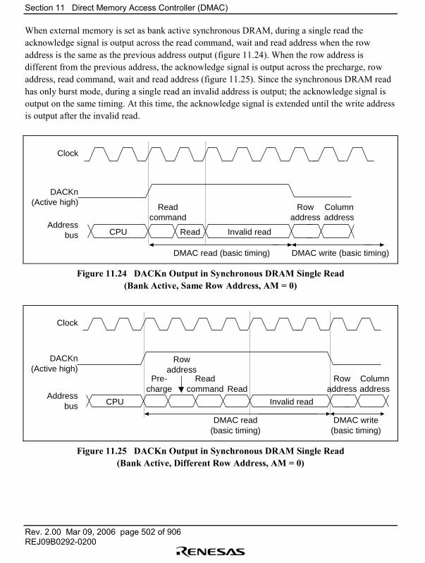
Section 11 Direct Memory Access Controller (DMAC)
Rev. 2.00 Mar 09, 2006 page 502 of 906REJ09B0292-0200
When external memory is set as bank active synchronous DRAM, during a single read theacknowledge signal is output across the read command, wait and read address when the rowaddress is the same as the previous address output (figure 11.24). When the row address isdifferent from the previous address, the acknowledge signal is output across the precharge, rowaddress, read command, wait and read address (figure 11.25). Since the synchronous DRAM readhas only burst mode, during a single read an invalid address is output; the acknowledge signal isoutput on the same timing. At this time, the acknowledge signal is extended until the write addressis output after the invalid read.
Clock
DACKn(Active high)
Addressbus CPU Read Invalid read
DMAC read (basic timing) DMAC write (basic timing)
Readcommand
Rowaddress
Columnaddress
Figure 11.24 DACKn Output in Synchronous DRAM Single Read(Bank Active, Same Row Address, AM = 0)
Clock
DACKn(Active high)
Addressbus CPU Invalid read
DMAC read(basic timing)
DMAC write(basic timing)
Rowaddress
Readcommand
Rowaddress
Columnaddress
Pre-charge Read
Figure 11.25 DACKn Output in Synchronous DRAM Single Read(Bank Active, Different Row Address, AM = 0)
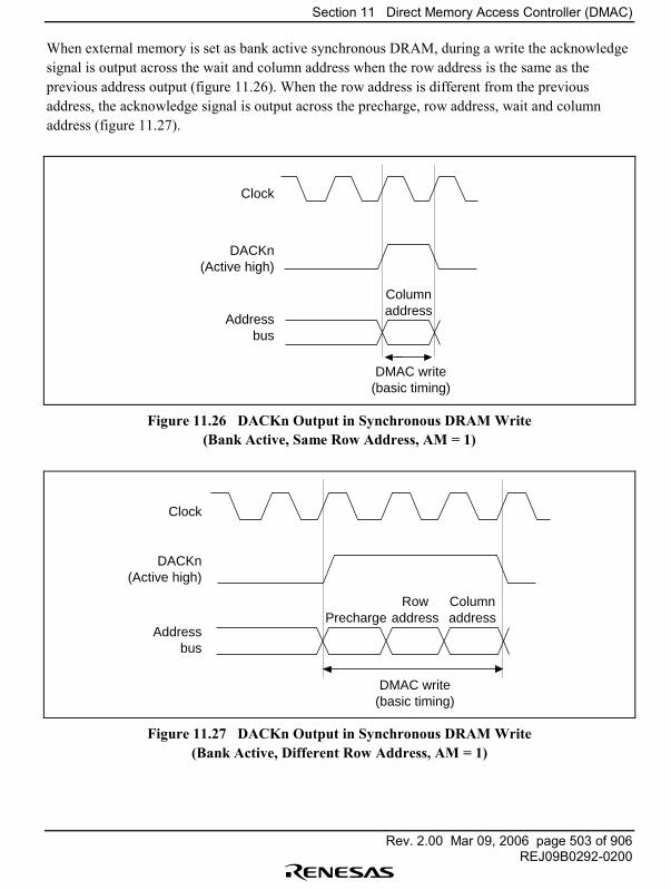
Section 11 Direct Memory Access Controller (DMAC)
Rev. 2.00 Mar 09, 2006 page 503 of 906REJ09B0292-0200
When external memory is set as bank active synchronous DRAM, during a write the acknowledgesignal is output across the wait and column address when the row address is the same as theprevious address output (figure 11.26). When the row address is different from the previousaddress, the acknowledge signal is output across the precharge, row address, wait and columnaddress (figure 11.27).
Clock
DACKn(Active high)
Addressbus
DMAC write(basic timing)
Columnaddress
Figure 11.26 DACKn Output in Synchronous DRAM Write(Bank Active, Same Row Address, AM = 1)
Clock
DACKn(Active high)
Addressbus
DMAC write(basic timing)
PrechargeRow
addressColumnaddress
Figure 11.27 DACKn Output in Synchronous DRAM Write(Bank Active, Different Row Address, AM = 1)
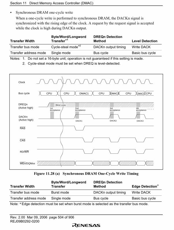
Section 11 Direct Memory Access Controller (DMAC)
Rev. 2.00 Mar 09, 2006 page 504 of 906REJ09B0292-0200
• Synchronous DRAM one-cycle writeWhen a one-cycle write is performed to synchronous DRAM, the DACKn signal issynchronized with the rising edge of the clock. A request by the request signal is acceptedwhile the clock is high during DACKn output.
Transfer WidthByte/Word/LongwordTransfer*1
DREQn DetectionMethod Level Detection
Transfer bus mode Cycle-steal mode*2 DACKn output timing Write DACK
Transfer address mode Single mode Bus cycle Basic bus cycleNotes: 1. Do not set a 16-byte unit; operation is not guaranteed if this setting is made.
2. Cycle-steal mode must be set when DREQ is level-detected.
Clock
Bus cycle
DREQn(Active high)
DMAC1 DMAC2 DMAC3
DACK1 DACK3DACK2
1stacceptance
CPU CPU CPU CPU CPU
DACKn(Active high)
CAS
RD/WR
WEn/DQMxx
RAS
Blind zone
. . . .2ndacceptance
3rdacceptance
4thacceptance
Figure 11.28 (a) Synchronous DRAM One-Cycle Write Timing
Transfer WidthByte/Word/LongwordTransfer
DREQn DetectionMethod Edge Detection*
Transfer bus mode Burst mode DACKn output timing Write DACK
Transfer address mode Single mode Bus cycle Basic bus cycleNote: * Edge detection must be set when burst mode is selected as the transfer bus mode.
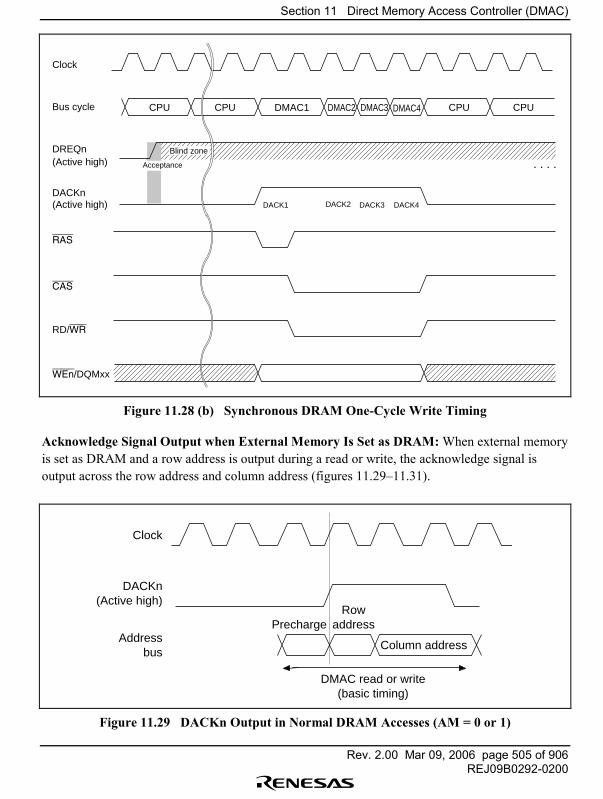
Section 11 Direct Memory Access Controller (DMAC)
Rev. 2.00 Mar 09, 2006 page 505 of 906REJ09B0292-0200
Clock
Bus cycle
DREQn(Active high)
DMAC1 DMAC2 DMAC3 DMAC4
DACK1 DACK3 DACK4DACK2
Acceptance
CPU CPU CPU CPU
DACKn(Active high)
CAS
RD/WR
WEn/DQMxx
RAS
. . . .Blind zone
Figure 11.28 (b) Synchronous DRAM One-Cycle Write Timing
Acknowledge Signal Output when External Memory Is Set as DRAM: When external memoryis set as DRAM and a row address is output during a read or write, the acknowledge signal isoutput across the row address and column address (figures 11.29�11.31).
Clock
DACKn(Active high)
Addressbus
DMAC read or write(basic timing)
PrechargeRow
address
Column address
Figure 11.29 DACKn Output in Normal DRAM Accesses (AM = 0 or 1)
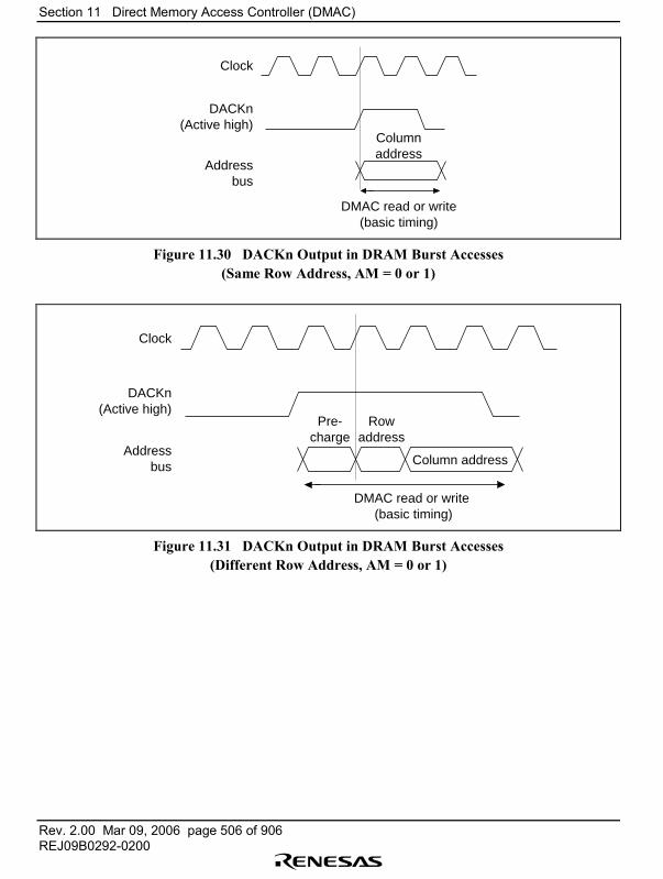
Section 11 Direct Memory Access Controller (DMAC)
Rev. 2.00 Mar 09, 2006 page 506 of 906REJ09B0292-0200
Clock
DACKn(Active high)
Addressbus
DMAC read or write(basic timing)
Columnaddress
Figure 11.30 DACKn Output in DRAM Burst Accesses(Same Row Address, AM = 0 or 1)
Clock
DACKn(Active high)
Addressbus
DMAC read or write (basic timing)
Pre-charge
Rowaddress
Column address
Figure 11.31 DACKn Output in DRAM Burst Accesses(Different Row Address, AM = 0 or 1)

Section 11 Direct Memory Access Controller (DMAC)
Rev. 2.00 Mar 09, 2006 page 507 of 906REJ09B0292-0200
Acknowledge Signal Output When External Memory Is Set as Burst ROM: When externalmemory is set as burst ROM, the acknowledge signal is output synchronous to the DMA address(no dual writes allowed) (figure 11.32).
Clock
DACKn(Active high)
Addressbus
DMAC (1 wait state)
DMAC cycle DMAC cycle
Figure 11.32 DACKn Output in Nibble Accesses of Burst ROM
11.3.7 DREQn Pin Input Detection Timing
In external request mode, DREQn pin signals are usually detected at the falling edge of the clockpulse (CKIO). When a request is detected, a DMAC bus cycle is produced four cycles later at theearliest and a DMA transfer performed. After the request is detected, the timing of the next inputdetection varies with the bus mode, address mode, DREQn input detection, and the memoryconnected.
DREQn Pin Input Detection Timing in Cycle-Steal Mode: In cycle-steal mode, once a requestis detected from the DREQn pin, the request signal is not detected until DACKn signal output inthe next external bus cycle. In cycle-steal mode, request detection is performed from DACKnsignal output until a request is detected.
Once a request has been accepted, it cannot be canceled midway.
The timing from the detection of a request until the next time requests are detectable is shownbelow.
• Cycle-Steal Mode Edge DetectionWhen transfer control is performed using edge detection, perform DREQn/DACKnhandshaking as shown in figure 11.33, and perform DREQn input control so that there is aone-to-one relationship between DREQn and DACKn. Operation is not guaranteed if DREQnis input before the corresponding DACKn is output.
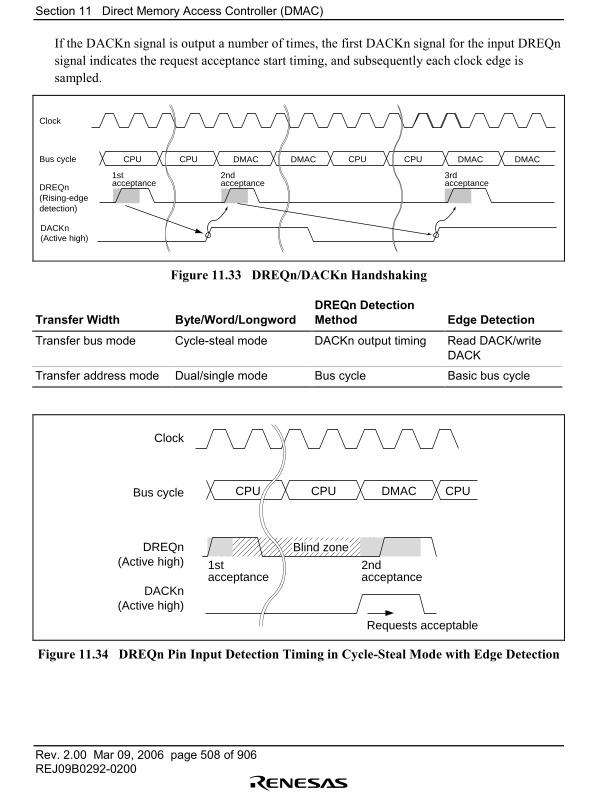
Section 11 Direct Memory Access Controller (DMAC)
Rev. 2.00 Mar 09, 2006 page 508 of 906REJ09B0292-0200
If the DACKn signal is output a number of times, the first DACKn signal for the input DREQnsignal indicates the request acceptance start timing, and subsequently each clock edge issampled.
Clock
DMAC DMAC DMAC DMAC
1st acceptance
2nd acceptance
3rdacceptance
CPU CPU CPU CPU
DACKn(Active high)
Bus cycle
DREQn (Rising-edge detection)
Figure 11.33 DREQn/DACKn Handshaking
Transfer Width Byte/Word/LongwordDREQn DetectionMethod Edge Detection
Transfer bus mode Cycle-steal mode DACKn output timing Read DACK/writeDACK
Transfer address mode Dual/single mode Bus cycle Basic bus cycle
Clock
Bus cycle
DREQn(Active high)
DACKn(Active high)
Requests acceptable
2ndacceptance
1stacceptance
CPU CPU DMAC CPU
Blind zone
Figure 11.34 DREQn Pin Input Detection Timing in Cycle-Steal Mode with Edge Detection
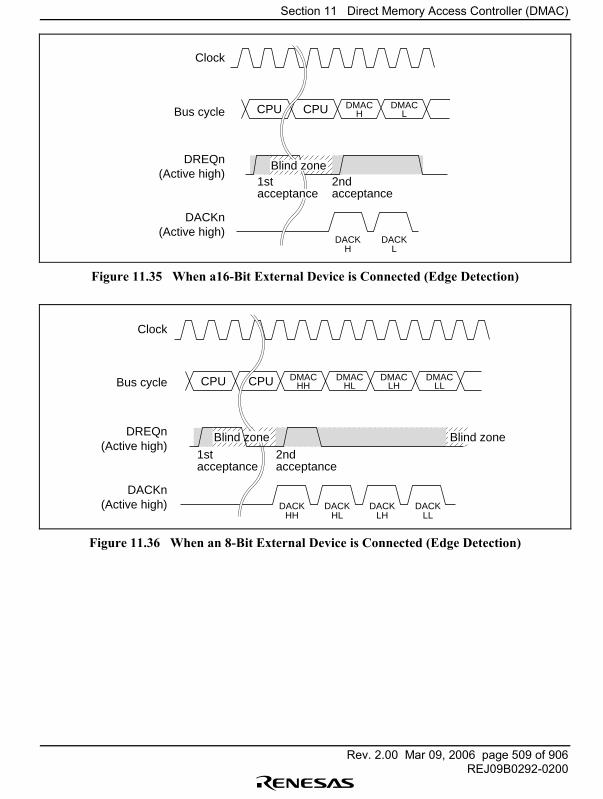
Section 11 Direct Memory Access Controller (DMAC)
Rev. 2.00 Mar 09, 2006 page 509 of 906REJ09B0292-0200
Clock
Bus cycle CPU DMACH
DMACL
DACKH
DACKL
2nd acceptance
CPU
DACKn(Active high)
DREQn(Active high)
1stacceptance
Blind zone
Figure 11.35 When a16-Bit External Device is Connected (Edge Detection)
Clock
Bus cycle CPU DMACHH
DACKHH
DACKHL
DACKLH
DACKLL
DMACHL
DMACLH
DMACLL
1st acceptance
2nd acceptance
CPU
Blind zone Blind zone
DACKn(Active high)
DREQn(Active high)
Figure 11.36 When an 8-Bit External Device is Connected (Edge Detection)
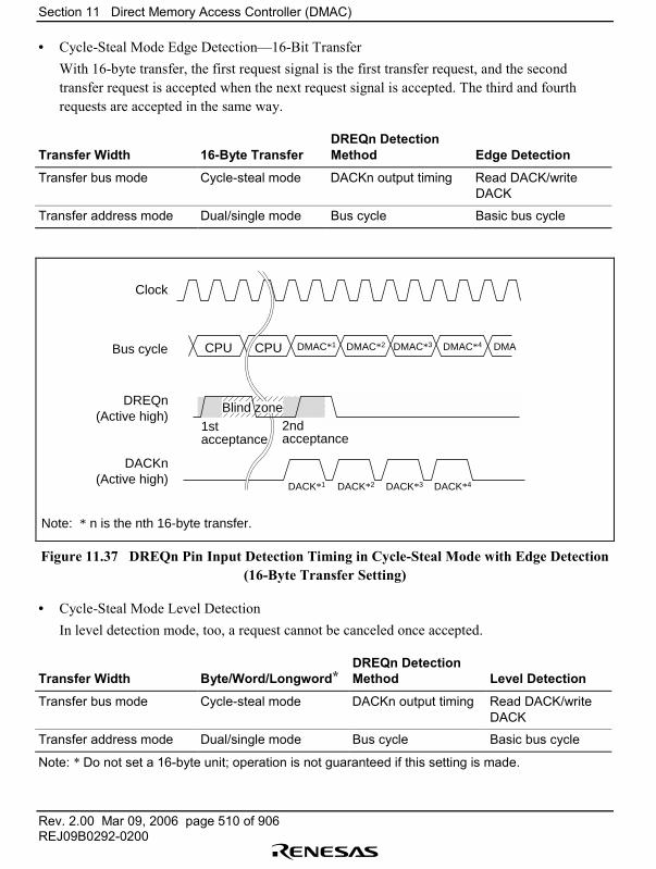
Section 11 Direct Memory Access Controller (DMAC)
Rev. 2.00 Mar 09, 2006 page 510 of 906REJ09B0292-0200
• Cycle-Steal Mode Edge Detection�16-Bit TransferWith 16-byte transfer, the first request signal is the first transfer request, and the secondtransfer request is accepted when the next request signal is accepted. The third and fourthrequests are accepted in the same way.
Transfer Width 16-Byte TransferDREQn DetectionMethod Edge Detection
Transfer bus mode Cycle-steal mode DACKn output timing Read DACK/writeDACK
Transfer address mode Dual/single mode Bus cycle Basic bus cycle
Clock
Bus cycle CPU CPU DMAC*1 DMAC*2 DMAC*3 DMAC*4 DMA
1stacceptance
2ndacceptance
DACK*1 DACK*2 DACK*3 DACK*4
Blind zone
Note: * n is the nth 16-byte transfer.
DACKn(Active high)
DREQn(Active high)
Figure 11.37 DREQn Pin Input Detection Timing in Cycle-Steal Mode with Edge Detection(16-Byte Transfer Setting)
• Cycle-Steal Mode Level DetectionIn level detection mode, too, a request cannot be canceled once accepted.
Transfer Width Byte/Word/Longword*DREQn DetectionMethod Level Detection
Transfer bus mode Cycle-steal mode DACKn output timing Read DACK/writeDACK
Transfer address mode Dual/single mode Bus cycle Basic bus cycle
Note: * Do not set a 16-byte unit; operation is not guaranteed if this setting is made.
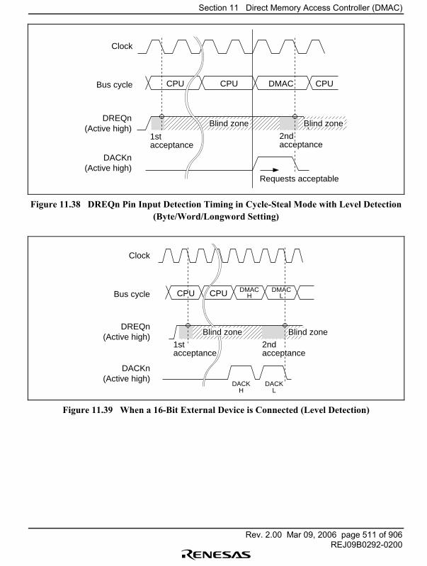
Section 11 Direct Memory Access Controller (DMAC)
Rev. 2.00 Mar 09, 2006 page 511 of 906REJ09B0292-0200
Clock
Bus cycle
Requests acceptable
1stacceptance
CPU CPU DMAC CPU
Blind zone Blind zone
2ndacceptance
DACKn(Active high)
DREQn(Active high)
Figure 11.38 DREQn Pin Input Detection Timing in Cycle-Steal Mode with Level Detection(Byte/Word/Longword Setting)
Clock
Bus cycleDMAC
H
DACKH
DACKL
1stacceptance
CPU
Blind zone Blind zone
2ndacceptance
DMACLCPU
DACKn(Active high)
DREQn(Active high)
Figure 11.39 When a 16-Bit External Device is Connected (Level Detection)
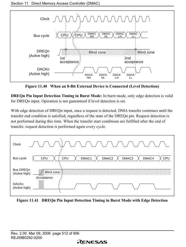
Section 11 Direct Memory Access Controller (DMAC)
Rev. 2.00 Mar 09, 2006 page 512 of 906REJ09B0292-0200
Clock
Bus cycleDMAC
HHDMAC
HLDMAC
LH
DACKHH
DACKHL
DACKLH
DACKLL
1st acceptance
CPU
DACKn
Blind zone Blind zone
2nd acceptance
DMACLLCPU
(Active high)
DREQn(Active high)
Figure 11.40 When an 8-Bit External Device is Connected (Level Detection)
DREQn Pin Input Detection Timing in Burst Mode: In burst mode, only edge detection is validfor DREQn input. Operation is not guaranteed if level detection is set.
With edge detection of DREQn input, once a request is detected, DMA transfer continues until thetransfer end condition is satisfied, regardless of the state of the DREQn pin. Request detection isnot performed during this time. When the transfer start conditions are fulfilled after the end oftransfer, request detection is performed again every cycle.
Clock
DMAC1 DMAC2CPU CPU CPUDMAC3 DMAC4
DACKn(Active high)
Blind zone
Acceptance
Bus cycle
Bus DREQn(Active high)
Figure 11.41 DREQn Pin Input Detection Timing in Burst Mode with Edge Detection
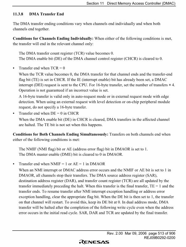
Section 11 Direct Memory Access Controller (DMAC)
Rev. 2.00 Mar 09, 2006 page 513 of 906REJ09B0292-0200
11.3.8 DMA Transfer End
The DMA transfer ending conditions vary when channels end individually and when bothchannels end together.
Conditions for Channels Ending Individually: When either of the following conditions is met,the transfer will end in the relevant channel only:
The DMA transfer count register (TCR) value becomes 0.The DMA enable bit (DE) of the DMA channel control register (CHCR) is cleared to 0.
• Transfer end when TCR = 0When the TCR value becomes 0, the DMA transfer for that channel ends and the transfer-endflag bit (TE) is set in CHCR. If the IE (interrupt enable) bit has already been set, a DMACinterrupt (DEI) request is sent to the CPU. For 16-byte transfer, set the number of transfers × 4.Operation is not guaranteed if an incorrect value is set.A 16-byte transfer is valid only in auto-request mode or in external request mode with edgedetection. When using an external request with level detection or on-chip peripheral modulerequest, do not specify a 16-byte transfer.
• Transfer end when DE = 0 in CHCRWhen the DMA enable bit (DE) in CHCR is cleared, DMA transfers in the affected channelare halted. The TE bit is not set when this happens.
Conditions for Both Channels Ending Simultaneously: Transfers on both channels end wheneither of the following conditions is met:
The NMIF (NMI flag) bit or AE (address error flag) bit in DMAOR is set to 1.The DMA master enable (DME) bit is cleared to 0 in DMAOR.
• Transfer end when NMIF = 1 or AE = 1 in DMAORWhen an NMI interrupt or DMAC address error occurs and the NMIF or AE bit is set to 1 inDMAOR, all channels stop their transfers. The DMA source address register (SAR),destination address register (DAR), and transfer count register (TCR) are all updated by thetransfer immediately preceding the halt. When this transfer is the final transfer, TE = 1 and thetransfer ends. To resume transfer after NMI interrupt exception handling or address errorexception handling, clear the appropriate flag bit. When the DE bit is then set to 1, the transferon that channel will restart. To avoid this, keep its DE bit at 0. In dual address mode, DMAtransfer will be halted after the completion of the following write cycle even when the addresserror occurs in the initial read cycle. SAR, DAR and TCR are updated by the final transfer.

Section 11 Direct Memory Access Controller (DMAC)
Rev. 2.00 Mar 09, 2006 page 514 of 906REJ09B0292-0200
• Transfer end when DME = 0 in DMAORClearing the DME bit in DMAOR forcibly aborts the transfers on both channels at the end ofthe current bus cycle. When the transfer is the final transfer, TE = 1 and the transfer ends.
11.3.9 BHBHBHBH Pin Output Timing
Purpose of New Specifications for BHBHBHBH: When the SH7616 is connected to the PCI bus as anexternal bus, Grew logic must be used externally because the SH7616 is not equipped with a PCIbus interface.
The PCI bus uses burst transfer principally, and performance is poor if data is transferred in smallincrements.
Due to these properties of the PCI bus, it is necessary to use Grew logic externally to compare thepresent address and the next address and determine whether burst transfer is possible. However,the size of the external Grew logic increases if address comparisons are required, and there is alsothe possibility that delays may interfere with timing requirements.
The specifications for BH have therefore been updated in order to solve these problems. Now ifburst transfer is possible using the present address this information is passed to the external Grewlogic. This provides enhanced support for PCI bus connections.
Register Settings When Using BHBHBHBH Pin: BH is output from only when the 16-byte transfer modeis selected using the DMAC built into the SH7616. However, it is not output when SDRAM orDRAM are accessed. When using the 16-byte transfer mode, specify auto-request mode or theexternal request mode with edge detection. If external request mode with level detection or on-chip module request mode is specified, operation is not guaranteed.
To use BH, the settings for the CHCR0 register or CHCR1 register in the on-chip DMAC of theSH7616 must be as shown in figure 11.43. BH is not output unless the settings for the CHCR0register or CHCR1 register are as indicated in figure 11.42.
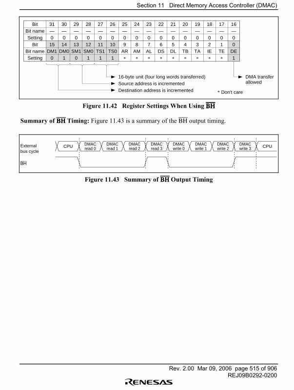
Section 11 Direct Memory Access Controller (DMAC)
Rev. 2.00 Mar 09, 2006 page 515 of 906REJ09B0292-0200
BitBit nameSetting
BitBit nameSetting
31—015
DM10
30—014
DM01
29—013
SM10
28—012
SM01
27—011
TS11
26—010
TS01
25—09
AR
*
24—08
AM
*
23—07
AL
*
22—06
DS
*
21—05
DL
*
20—04
TB
*
19—03
TA
*
18—02IE
*
17—01
TE
*
16—00
DE1
16-byte unit (four long words transferred)Source address is incrementedDestination address is incremented * Don't care
DMA transferallowed
Figure 11.42 Register Settings When Using BHBHBHBH
Summary of BHBHBHBH Timing: Figure 11.43 is a summary of the BH output timing.
CPU DMACread 0
DMACread 1
DMACread 2
DMACread 3
DMACwrite 0
DMACwrite 1
DMACwrite 2
DMACwrite 3 CPUExternal
bus cycle
BH
Figure 11.43 Summary of BHBHBHBH Output Timing
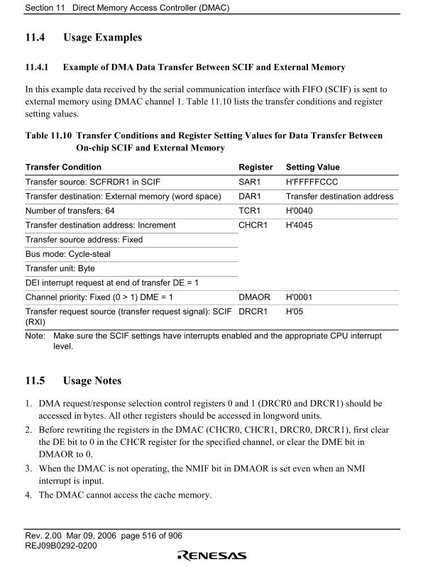
Section 11 Direct Memory Access Controller (DMAC)
Rev. 2.00 Mar 09, 2006 page 516 of 906REJ09B0292-0200
11.4 Usage Examples
11.4.1 Example of DMA Data Transfer Between SCIF and External Memory
In this example data received by the serial communication interface with FIFO (SCIF) is sent toexternal memory using DMAC channel 1. Table 11.10 lists the transfer conditions and registersetting values.
Table 11.10 Transfer Conditions and Register Setting Values for Data Transfer BetweenOn-chip SCIF and External Memory
Transfer Condition Register Setting Value
Transfer source: SCFRDR1 in SCIF SAR1 H'FFFFFCCC
Transfer destination: External memory (word space) DAR1 Transfer destination address
Number of transfers: 64 TCR1 H'0040
Transfer destination address: Increment CHCR1 H'4045
Transfer source address: Fixed
Bus mode: Cycle-steal
Transfer unit: Byte
DEI interrupt request at end of transfer DE = 1
Channel priority: Fixed (0 > 1) DME = 1 DMAOR H'0001
Transfer request source (transfer request signal): SCIF(RXI)
DRCR1 H'05
Note: Make sure the SCIF settings have interrupts enabled and the appropriate CPU interruptlevel.
11.5 Usage Notes
1. DMA request/response selection control registers 0 and 1 (DRCR0 and DRCR1) should beaccessed in bytes. All other registers should be accessed in longword units.
2. Before rewriting the registers in the DMAC (CHCR0, CHCR1, DRCR0, DRCR1), first clearthe DE bit to 0 in the CHCR register for the specified channel, or clear the DME bit inDMAOR to 0.
3. When the DMAC is not operating, the NMIF bit in DMAOR is set even when an NMIinterrupt is input.
4. The DMAC cannot access the cache memory.
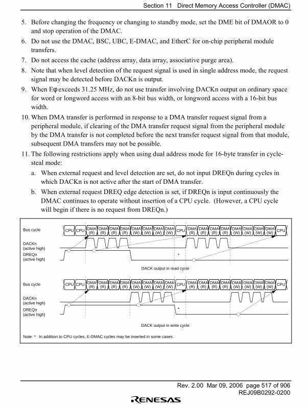
Section 11 Direct Memory Access Controller (DMAC)
Rev. 2.00 Mar 09, 2006 page 517 of 906REJ09B0292-0200
5. Before changing the frequency or changing to standby mode, set the DME bit of DMAOR to 0and stop operation of the DMAC.
6. Do not use the DMAC, BSC, UBC, E-DMAC, and EtherC for on-chip peripheral moduletransfers.
7. Do not access the cache (address array, data array, associative purge area).8. Note that when level detection of the request signal is used in single address mode, the request
signal may be detected before DACKn is output.9. When Eφ exceeds 31.25 MHz, do not use transfer involving DACKn output on ordinary space
for word or longword access with an 8-bit bus width, or longword access with a 16-bit buswidth.
10. When DMA transfer is performed in response to a DMA transfer request signal from aperipheral module, if clearing of the DMA transfer request signal from the peripheral moduleby the DMA transfer is not completed before the next transfer request signal from that module,subsequent DMA transfers may not be possible.
11. The following restrictions apply when using dual address mode for 16-byte transfer in cycle-steal mode:a. When external request and level detection are set, do not input DREQn during cycles in
which DACKn is not active after the start of DMA transfer.b. When external request DREQ edge detection is set, if DREQn is input continuously the
DMAC continues to operate without insertion of a CPU cycle. (However, a CPU cyclewill begin if there is no request from DREQn.)
Bus cycle
Note: * In addition to CPU cycles, E-DMAC cycles may be inserted in some cases.
DACK output in read cycle
CPU CPU CPU CPUDMA(W)
DMA(W)
DMA(W)
DMA(W)
DMA(R)
DMA(R)
DMA(R)
DMA(R)
DMA(W)
DMA(W)
DMA(W)
DMA(W)
DMA(R)
DMA(R)
DMA(R)
DMA(R)
CPU CPU CPU CPUDMA(W)
DMA(W)
DMA(W)
DMA(W)
DMA(R)
DMA(R)
DMA(R)
DMA(R)
DMA(W)
DMA(W)
DMA(W)
DMA(W)
DMA(R)
DMA(R)
DMA(R)
DMA(R)
DACK output in write cycle
DACKn(active high)
DREQn(active high)
Bus cycle
DACKn(active high)
DREQn(active high)
*
*
Section 11 Direct Memory Access Controller (DMAC)
Rev. 2.00 Mar 09, 2006 page 518 of 906REJ09B0292-0200
12. When setting DMAC channel 0 to cycle-steal mode, and channel 1 to cycle-steel mode, dualaddress mode or built-in peripheral module request, set the priority mode to priority orderfixed mode.
13. When SDRAM is connected, set the upper limit of external bus frequency in DMA singleaddress mode transfers to 31.25 MHz.
14. In the dual address mode, bits TS1 and TS0 (transfer size) in CHCR0 and CHCR1 should becleared to 00 (byte unit setting) if a destination address as been set in internal memory.
Section 12 16-Bit Free-Running Timer (FRT)
Rev. 2.00 Mar 09, 2006 page 519 of 906REJ09B0292-0200
Section 12 16-Bit Free-Running Timer (FRT)
12.1 Overview
A single-channel, 16-bit free-running timer (FRT) is included on-chip. The FRT is based on a16-bit free-running counter (FRC) and can output two types of independent waveforms. The FRTcan also measure the width of input pulses and the cycle of external clocks.
12.1.1 Features
The FRT has the following features:
• Choice of four counter input clocksThe counter input clock can be selected from three internal clocks (Pφ/8, Pφ/32, Pφ/128) andan external clock (enabling external event counting).
• Two independent comparatorsTwo waveform outputs can be generated.
• Input captureChoice of rising edge or falling edge
• Counter clear specificationThe counter value can be cleared by compare match A.
• Four interrupt sourcesTwo compare match sources, one input capture source, and one overflow source can issue requestsindependently.
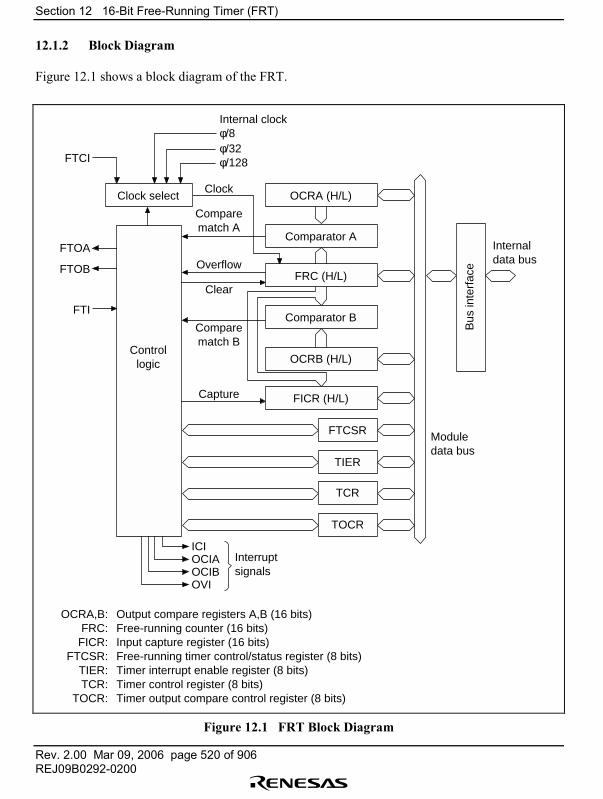
Section 12 16-Bit Free-Running Timer (FRT)
Rev. 2.00 Mar 09, 2006 page 520 of 906REJ09B0292-0200
12.1.2 Block Diagram
Figure 12.1 shows a block diagram of the FRT.
FTI
φ/8Internal clock
Internaldata bus
Moduledata bus
φ/32φ/128
ICIInterruptsignals
OCIAOCIBOVI
FTOB
FTOA
FTCI
Controllogic
Clock selectClock
Comparematch A
Overflow
Clear
Comparematch B
Capture
OCRA (H/L)
Comparator A
FRC (H/L)
Comparator B
OCRB (H/L)
FICR (H/L)
FTCSR
TIER
TCR
TOCR
Bus
inte
rfac
e
OCRA,B:FRC:FICR:
FTCSR:TIER:TCR:
TOCR:
Output compare registers A,B (16 bits)Free-running counter (16 bits)Input capture register (16 bits)Free-running timer control/status register (8 bits)Timer interrupt enable register (8 bits)Timer control register (8 bits)Timer output compare control register (8 bits)
Figure 12.1 FRT Block Diagram
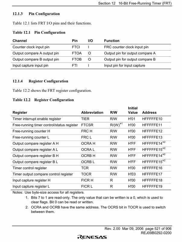
Section 12 16-Bit Free-Running Timer (FRT)
Rev. 2.00 Mar 09, 2006 page 521 of 906REJ09B0292-0200
12.1.3 Pin Configuration
Table 12.1 lists FRT I/O pins and their functions.
Table 12.1 Pin Configuration
Channel Pin I/O Function
Counter clock input pin FTCI I FRC counter clock input pin
Output compare A output pin FTOA O Output pin for output compare A
Output compare B output pin FTOB O Output pin for output compare B
Input capture input pin FTI I Input pin for input capture
12.1.4 Register Configuration
Table 12.2 shows the FRT register configuration.
Table 12.2 Register Configuration
Register Abbreviation R/WInitialValue Address
Timer interrupt enable register TIER R/W H'01 HFFFFFE10
Free-running timer control/status register FTCSR R/(W)*1 H'00 HFFFFFE11
Free-running counter H FRC H R/W H'00 HFFFFFE12
Free-running counter L FRC L R/W H'00 HFFFFFE13
Output compare register A H OCRA H R/W H'FF HFFFFFE14*2
Output compare register A L OCRA L R/W H'FF HFFFFFE15*2
Output compare register B H OCRB H R/W H'FF HFFFFFE14*2
Output compare register B L OCRB L R/W H'FF HFFFFFE15*2
Timer control register TCR R/W H'00 HFFFFFE16
Timer output compare control register TOCR R/W H'E0 HFFFFFE17
Input capture register H FICR H R H'00 HFFFFFE18
Input capture register L FICR L R H'00 HFFFFFE19Notes: Use byte-size access for all registers.
1. Bits 7 to 1 are read-only. The only value that can be written is a 0, which is used toclear flags. Bit 0 can be read or written.
2. OCRA and OCRB have the same address. The OCRS bit in TOCR is used to switchbetween them.
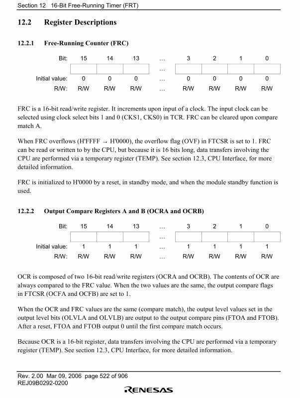
Section 12 16-Bit Free-Running Timer (FRT)
Rev. 2.00 Mar 09, 2006 page 522 of 906REJ09B0292-0200
12.2 Register Descriptions
12.2.1 Free-Running Counter (FRC)
Bit: 15 14 13 � 3 2 1 0
�
Initial value: 0 0 0 � 0 0 0 0
R/W: R/W R/W R/W � R/W R/W R/W R/W
FRC is a 16-bit read/write register. It increments upon input of a clock. The input clock can beselected using clock select bits 1 and 0 (CKS1, CKS0) in TCR. FRC can be cleared upon comparematch A.
When FRC overflows (H'FFFF → H'0000), the overflow flag (OVF) in FTCSR is set to 1. FRCcan be read or written to by the CPU, but because it is 16 bits long, data transfers involving theCPU are performed via a temporary register (TEMP). See section 12.3, CPU Interface, for moredetailed information.
FRC is initialized to H'0000 by a reset, in standby mode, and when the module standby function isused.
12.2.2 Output Compare Registers A and B (OCRA and OCRB)
Bit: 15 14 13 � 3 2 1 0
�
Initial value: 1 1 1 � 1 1 1 1
R/W: R/W R/W R/W � R/W R/W R/W R/W
OCR is composed of two 16-bit read/write registers (OCRA and OCRB). The contents of OCR arealways compared to the FRC value. When the two values are the same, the output compare flagsin FTCSR (OCFA and OCFB) are set to 1.
When the OCR and FRC values are the same (compare match), the output level values set in theoutput level bits (OLVLA and OLVLB) are output to the output compare pins (FTOA and FTOB).After a reset, FTOA and FTOB output 0 until the first compare match occurs.
Because OCR is a 16-bit register, data transfers involving the CPU are performed via a temporaryregister (TEMP). See section 12.3, CPU Interface, for more detailed information.
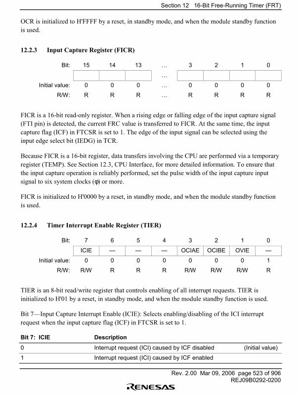
Section 12 16-Bit Free-Running Timer (FRT)
Rev. 2.00 Mar 09, 2006 page 523 of 906REJ09B0292-0200
OCR is initialized to H'FFFF by a reset, in standby mode, and when the module standby functionis used.
12.2.3 Input Capture Register (FICR)
Bit: 15 14 13 � 3 2 1 0
�
Initial value: 0 0 0 � 0 0 0 0
R/W: R R R � R R R R
FICR is a 16-bit read-only register. When a rising edge or falling edge of the input capture signal(FTI pin) is detected, the current FRC value is transferred to FICR. At the same time, the inputcapture flag (ICF) in FTCSR is set to 1. The edge of the input signal can be selected using theinput edge select bit (IEDG) in TCR.
Because FICR is a 16-bit register, data transfers involving the CPU are performed via a temporaryregister (TEMP). See Section 12.3, CPU Interface, for more detailed information. To ensure thatthe input capture operation is reliably performed, set the pulse width of the input capture inputsignal to six system clocks (φ) or more.
FICR is initialized to H'0000 by a reset, in standby mode, and when the module standby functionis used.
12.2.4 Timer Interrupt Enable Register (TIER)
Bit: 7 6 5 4 3 2 1 0
ICIE � � � OCIAE OCIBE OVIE �
Initial value: 0 0 0 0 0 0 0 1
R/W: R/W R R R R/W R/W R/W R
TIER is an 8-bit read/write register that controls enabling of all interrupt requests. TIER isinitialized to H'01 by a reset, in standby mode, and when the module standby function is used.
Bit 7�Input Capture Interrupt Enable (ICIE): Selects enabling/disabling of the ICI interruptrequest when the input capture flag (ICF) in FTCSR is set to 1.
Bit 7: ICIE Description
0 Interrupt request (ICI) caused by ICF disabled (Initial value)
1 Interrupt request (ICI) caused by ICF enabled
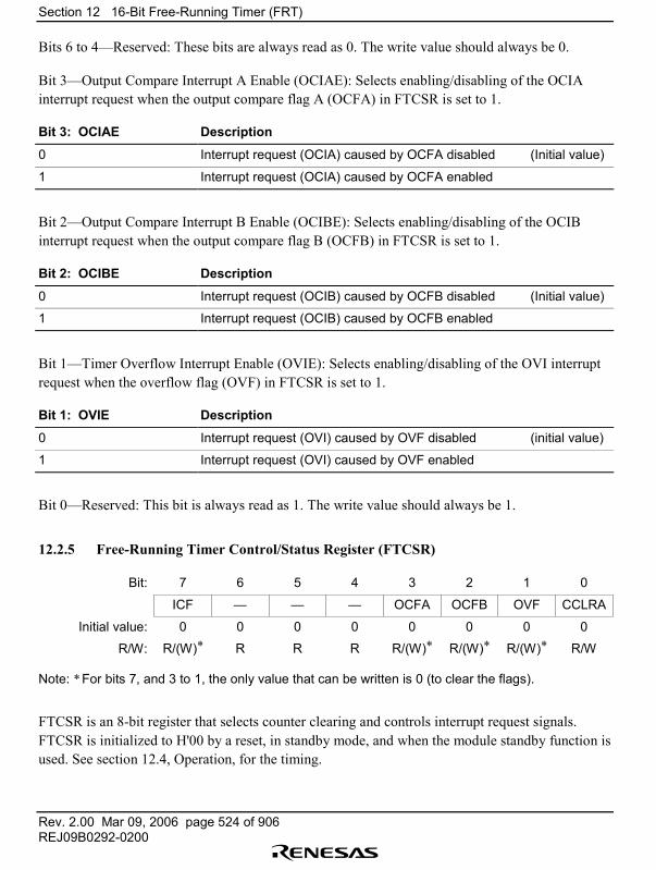
Section 12 16-Bit Free-Running Timer (FRT)
Rev. 2.00 Mar 09, 2006 page 524 of 906REJ09B0292-0200
Bits 6 to 4�Reserved: These bits are always read as 0. The write value should always be 0.
Bit 3�Output Compare Interrupt A Enable (OCIAE): Selects enabling/disabling of the OCIAinterrupt request when the output compare flag A (OCFA) in FTCSR is set to 1.
Bit 3: OCIAE Description
0 Interrupt request (OCIA) caused by OCFA disabled (Initial value)
1 Interrupt request (OCIA) caused by OCFA enabled
Bit 2�Output Compare Interrupt B Enable (OCIBE): Selects enabling/disabling of the OCIBinterrupt request when the output compare flag B (OCFB) in FTCSR is set to 1.
Bit 2: OCIBE Description
0 Interrupt request (OCIB) caused by OCFB disabled (Initial value)
1 Interrupt request (OCIB) caused by OCFB enabled
Bit 1�Timer Overflow Interrupt Enable (OVIE): Selects enabling/disabling of the OVI interruptrequest when the overflow flag (OVF) in FTCSR is set to 1.
Bit 1: OVIE Description
0 Interrupt request (OVI) caused by OVF disabled (initial value)
1 Interrupt request (OVI) caused by OVF enabled
Bit 0�Reserved: This bit is always read as 1. The write value should always be 1.
12.2.5 Free-Running Timer Control/Status Register (FTCSR)
Bit: 7 6 5 4 3 2 1 0
ICF � � � OCFA OCFB OVF CCLRA
Initial value: 0 0 0 0 0 0 0 0
R/W: R/(W)* R R R R/(W)* R/(W)* R/(W)* R/W
Note: * For bits 7, and 3 to 1, the only value that can be written is 0 (to clear the flags).
FTCSR is an 8-bit register that selects counter clearing and controls interrupt request signals.FTCSR is initialized to H'00 by a reset, in standby mode, and when the module standby function isused. See section 12.4, Operation, for the timing.
Section 12 16-Bit Free-Running Timer (FRT)
Rev. 2.00 Mar 09, 2006 page 525 of 906REJ09B0292-0200
Bit 7�Input Capture Flag (ICF): Status flag that indicates that the FRC value has been sent toFICR by the input capture signal. This flag is cleared by software and set by hardware. It cannotbe set by software.
Bit 7: ICF Description
0 [Clearing condition]
When ICF is read while set to 1, and then 0 is written to it(Initial value)
1 [Setting condition]
When the FRC value is sent to FICR by the input capture signal
Bits 6 to 4�Reserved: These bits always read 0. The write value should always be 0.
Bit 3�Output Compare Flag A (OCFA): Status flag that indicates when the values of the FRCand OCRA match. This flag is cleared by software and set by hardware. It cannot be set bysoftware.
Bit 3: OCFA Description
0 [Clearing condition]
When OCFA is read while set to 1, and then 0 is written to it(Initial value)
1 [Setting condition]
When the FRC value becomes equal to OCRA
Bit 2�Output Compare Flag B (OCFB): Status flag that indicates when the values of FRC andOCRB match. This flag is cleared by software and set by hardware. It cannot be set by software.
Bit 2: OCFB Description
0 [Clearing condition]
When OCFB is read while set to 1, and then 0 is written to it(Initial value)
1 [Setting condition]
When the FRC value becomes equal to OCRB
Section 12 16-Bit Free-Running Timer (FRT)
Rev. 2.00 Mar 09, 2006 page 526 of 906REJ09B0292-0200
Bit 1�Timer Overflow Flag (OVF): Status flag that indicates when FRC overflows (from H'FFFFto H'0000). This flag is cleared by software and set by hardware. It cannot be set by software.
Bit 1: OVF Description
0 [Clearing condition]
When OVF is read while set to 1, and then 0 is written to it(Initial value)
1 [Setting condition]
When the FRC value changes from H'FFFF to H'0000
Bit 0�Counter Clear A (CCLRA): Selects whether or not to clear FRC on compare match A(signal indicating match of FRC and OCRA).
Bit 0: CCLRA Description
0 FRC clear disabled (Initial value)
1 FRC cleared on compare match A
12.2.6 Timer Control Register (TCR)
Bit: 7 6 5 4 3 2 1 0
IEDG � � � � � CKS1 CKS0
Initial value: 0 0 0 0 0 0 0 0
R/W: R/W R R R R R R/W R/W
TCR is an 8-bit read/write register that selects the input edge for input capture and selects theinput clock for FRC. TCR is initialized to H'00 by a reset, in standby mode, and when the modulestandby function is used.
Bit 7�Input Edge Select (IEDG): Selects whether to capture the input capture input (FTI) on thefalling edge or rising edge.
Bit 7: IEDG Description
0 Input captured on falling edge (Initial value)
1 Input captured on rising edge
Bits 6 to 2�Reserved: These bits are always read as 0. The write value should always be 0.

Section 12 16-Bit Free-Running Timer (FRT)
Rev. 2.00 Mar 09, 2006 page 527 of 906REJ09B0292-0200
Bits 1 and 0�Clock Select (CKS1, CKS0): These bits select whether to use an external clock orone of three internal clocks for input to FRC. The external clock is counted at the rising edge.
Bit 1: CKS1 Bit 0: CKS0 Description
0 0 Internal clock: count at φ/8 (Initial value)
1 Internal clock: count at φ/32
1 0 Internal clock: count at φ/128
1 External clock: count at rising edge
12.2.7 Timer Output Compare Control Register (TOCR)
Bit: 7 6 5 4 3 2 1 0
� � � OCRS � � OLVLA OLVLB
Initial value: 1 1 1 0 0 0 0 0
R/W: R R R R/W R R R/W R/W
TOCR is an 8-bit read/write register that selects the output level for output compare and controlsswitching between access of output compare registers A and B. TOCR is initialized to H'E0 by areset, in standby mode, and when the module standby function is used.
Bits 7 to 5�Reserved: These bits are always read as 1. The write value should always be 1.
Bit 4�Output Compare Register Select (OCRS): OCRA and OCRB share the same address. TheOCRS bit controls which register is selected when reading/writing to this address. It does notaffect the operation of OCRA and OCRB.
Bit 4: OCRS Description
0 OCRA register selected (Initial value)
1 OCRB register selected
Bits 3 and 2�Reserved: These bits are always read as 0. The write value should always be 0.
Bit 1�Output Level A (OLVLA): Selects the level output to the output compare A output pinupon compare match A (signal indicating match of FRC and OCRA).
Bit 1: OLVLA Description
0 0 output on compare match A (Initial value)
1 1 output on compare match A
Section 12 16-Bit Free-Running Timer (FRT)
Rev. 2.00 Mar 09, 2006 page 528 of 906REJ09B0292-0200
Bit 0�Output Level B (OLVLB): Selects the level output to the output compare B output pinupon compare match B (signal indicating match of FRC and OCRB).
Bit 0: OLVLB Description
0 0 output on compare match B (Initial value)
1 1 output on compare match B
12.3 CPU Interface
FRC, OCRA, OCRB, and FICR are 16-bit registers. The data bus width between the CPU andFRT, however, is only 8 bits. Access of these three types of registers from the CPU thereforeneeds to be performed via an 8-bit temporary register called TEMP.
The following describes how these registers are read from and written to:
• Writing to 16-bit RegistersThe upper byte is written, which results in the upper byte of data being stored in TEMP. Thelower byte is then written, which results in 16 bits of data being written to the register whencombined with the upper byte value in TEMP.
• Reading from 16-bit RegistersThe upper byte of data is read, which results in the upper byte value being transferred to theCPU. The lower byte value is transferred to TEMP. The lower byte is then read, which resultsin the lower byte value in TEMP being sent to the CPU.
When registers of these three types are accessed, two byte accesses should always be performed,first to the upper byte, then the lower byte. If only the upper byte or lower byte is accessed, thedata will not be transferred properly.
Figure 12.2 and 12.3 show the flow of data when FRC is accessed. Other registers function in thesame way. When reading OCRA and OCRB, however, both upper and lower-byte data istransferred directly to the CPU without passing through TEMP.
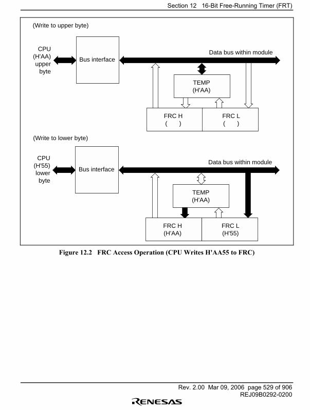
Section 12 16-Bit Free-Running Timer (FRT)
Rev. 2.00 Mar 09, 2006 page 529 of 906REJ09B0292-0200
CPU(H'AA)upper
byte
Data bus within moduleBus interface
TEMP(H'AA)
FRC H( )
FRC L( )
(Write to upper byte)
CPU(H'55)lowerbyte
Data bus within moduleBus interface
TEMP(H'AA)
FRC H(H'AA)
FRC L(H'55)
(Write to lower byte)
Figure 12.2 FRC Access Operation (CPU Writes H'AA55 to FRC)
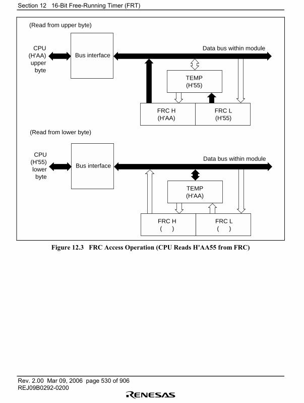
Section 12 16-Bit Free-Running Timer (FRT)
Rev. 2.00 Mar 09, 2006 page 530 of 906REJ09B0292-0200
CPU(H'AA)upper
byteTEMP(H'55)
FRC H(H'AA)
FRC L(H'55)
Data bus within moduleBus interface
(Read from upper byte)
CPU(H'55)lowerbyte
TEMP(H'AA)
FRC H( )
FRC L( )
Data bus within moduleBus interface
(Read from lower byte)
Figure 12.3 FRC Access Operation (CPU Reads H'AA55 from FRC)
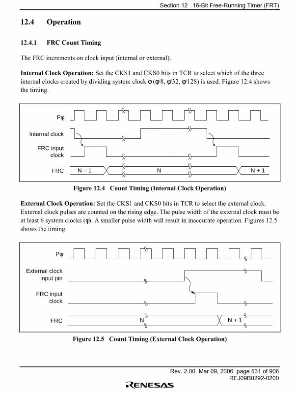
Section 12 16-Bit Free-Running Timer (FRT)
Rev. 2.00 Mar 09, 2006 page 531 of 906REJ09B0292-0200
12.4 Operation
12.4.1 FRC Count Timing
The FRC increments on clock input (internal or external).
Internal Clock Operation: Set the CKS1 and CKS0 bits in TCR to select which of the threeinternal clocks created by dividing system clock φ (φ/8, φ/32, φ/128) is used. Figure 12.4 showsthe timing.
Pφ
N – 1 N N + 1
Internal clock
FRC inputclock
FRC
Figure 12.4 Count Timing (Internal Clock Operation)
External Clock Operation: Set the CKS1 and CKS0 bits in TCR to select the external clock.External clock pulses are counted on the rising edge. The pulse width of the external clock must beat least 6 system clocks (φ). A smaller pulse width will result in inaccurate operation. Figures 12.5shows the timing.
N + 1N
Pφ
External clockinput pin
FRC inputclock
FRC
Figure 12.5 Count Timing (External Clock Operation)
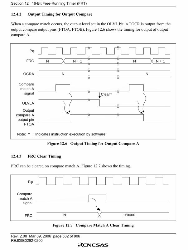
Section 12 16-Bit Free-Running Timer (FRT)
Rev. 2.00 Mar 09, 2006 page 532 of 906REJ09B0292-0200
12.4.2 Output Timing for Output Compare
When a compare match occurs, the output level set in the OLVL bit in TOCR is output from theoutput compare output pins (FTOA, FTOB). Figure 12.6 shows the timing for output of outputcompare A.
Clear*
N N
N NN + 1 N + 1
Pφ
FRC
OCRA
Comparematch A
signal
OLVLA
Outputcompare Aoutput pin
FTOA
Note: * ↓ Indicates instruction execution by software
Figure 12.6 Output Timing for Output Compare A
12.4.3 FRC Clear Timing
FRC can be cleared on compare match A. Figure 12.7 shows the timing.
Pφ
Comparematch A
signal
FRC N H'0000
Figure 12.7 Compare Match A Clear Timing
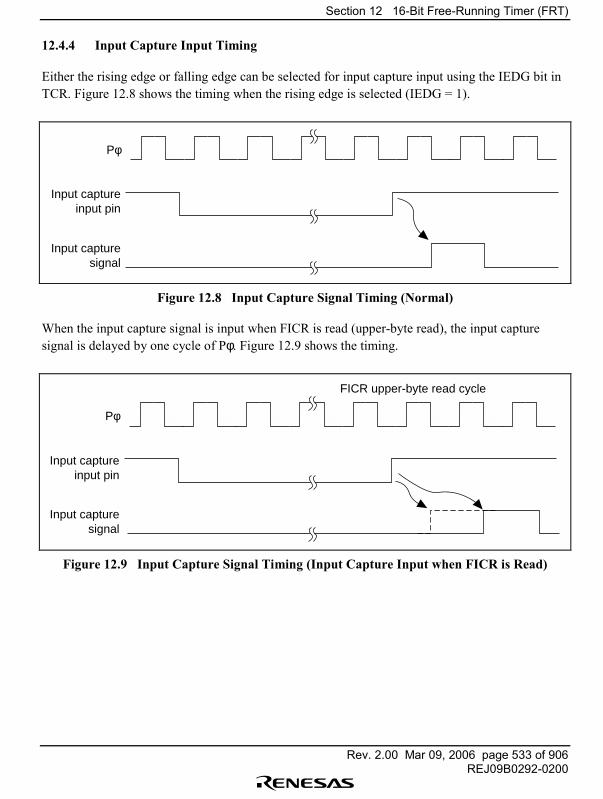
Section 12 16-Bit Free-Running Timer (FRT)
Rev. 2.00 Mar 09, 2006 page 533 of 906REJ09B0292-0200
12.4.4 Input Capture Input Timing
Either the rising edge or falling edge can be selected for input capture input using the IEDG bit inTCR. Figure 12.8 shows the timing when the rising edge is selected (IEDG = 1).
Pφ
Input captureinput pin
Input capturesignal
Figure 12.8 Input Capture Signal Timing (Normal)
When the input capture signal is input when FICR is read (upper-byte read), the input capturesignal is delayed by one cycle of Pφ. Figure 12.9 shows the timing.
Pφ
Input captureinput pin
Input capturesignal
FICR upper-byte read cycle
Figure 12.9 Input Capture Signal Timing (Input Capture Input when FICR is Read)
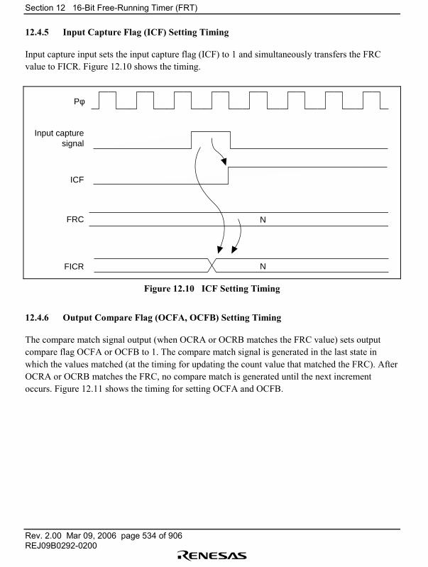
Section 12 16-Bit Free-Running Timer (FRT)
Rev. 2.00 Mar 09, 2006 page 534 of 906REJ09B0292-0200
12.4.5 Input Capture Flag (ICF) Setting Timing
Input capture input sets the input capture flag (ICF) to 1 and simultaneously transfers the FRCvalue to FICR. Figure 12.10 shows the timing.
Pφ
Input capturesignal
ICF
FRC
FICR N
N
Figure 12.10 ICF Setting Timing
12.4.6 Output Compare Flag (OCFA, OCFB) Setting Timing
The compare match signal output (when OCRA or OCRB matches the FRC value) sets outputcompare flag OCFA or OCFB to 1. The compare match signal is generated in the last state inwhich the values matched (at the timing for updating the count value that matched the FRC). AfterOCRA or OCRB matches the FRC, no compare match is generated until the next incrementoccurs. Figure 12.11 shows the timing for setting OCFA and OCFB.
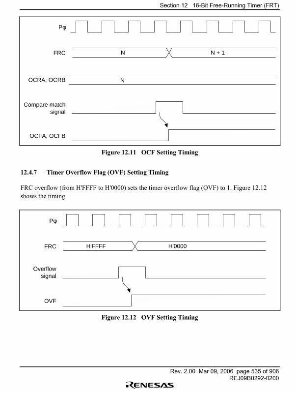
Section 12 16-Bit Free-Running Timer (FRT)
Rev. 2.00 Mar 09, 2006 page 535 of 906REJ09B0292-0200
Pφ
FRC
OCRA, OCRB
Compare matchsignal
OCFA, OCFB
N + 1N
N
Figure 12.11 OCF Setting Timing
12.4.7 Timer Overflow Flag (OVF) Setting Timing
FRC overflow (from H'FFFF to H'0000) sets the timer overflow flag (OVF) to 1. Figure 12.12shows the timing.
Pφ
FRC
Overflowsignal
OVF
H'0000H'FFFF
Figure 12.12 OVF Setting Timing
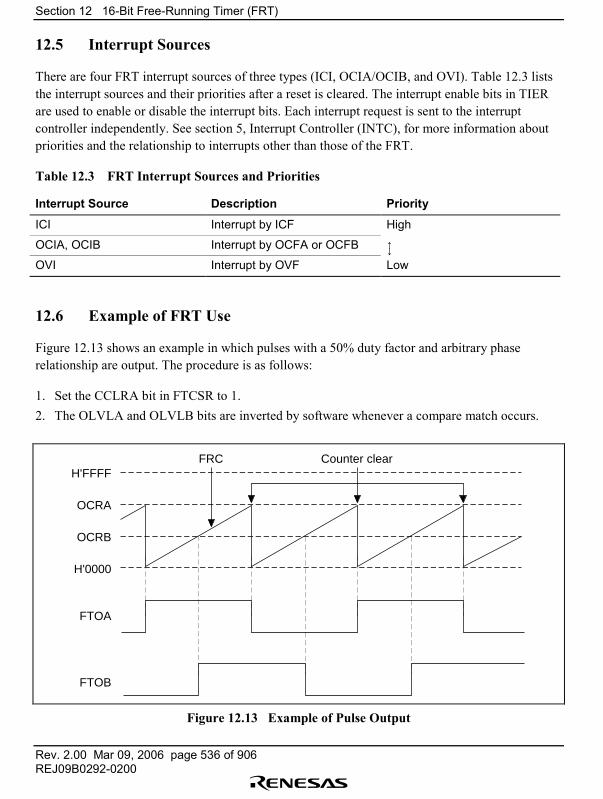
Section 12 16-Bit Free-Running Timer (FRT)
Rev. 2.00 Mar 09, 2006 page 536 of 906REJ09B0292-0200
12.5 Interrupt Sources
There are four FRT interrupt sources of three types (ICI, OCIA/OCIB, and OVI). Table 12.3 liststhe interrupt sources and their priorities after a reset is cleared. The interrupt enable bits in TIERare used to enable or disable the interrupt bits. Each interrupt request is sent to the interruptcontroller independently. See section 5, Interrupt Controller (INTC), for more information aboutpriorities and the relationship to interrupts other than those of the FRT.
Table 12.3 FRT Interrupt Sources and Priorities
Interrupt Source Description Priority
ICI Interrupt by ICF High
OCIA, OCIB Interrupt by OCFA or OCFB ↑↓OVI Interrupt by OVF Low
12.6 Example of FRT Use
Figure 12.13 shows an example in which pulses with a 50% duty factor and arbitrary phaserelationship are output. The procedure is as follows:
1. Set the CCLRA bit in FTCSR to 1.2. The OLVLA and OLVLB bits are inverted by software whenever a compare match occurs.
H'FFFF
OCRA
OCRB
H'0000
FTOA
FTOB
FRC Counter clear
Figure 12.13 Example of Pulse Output
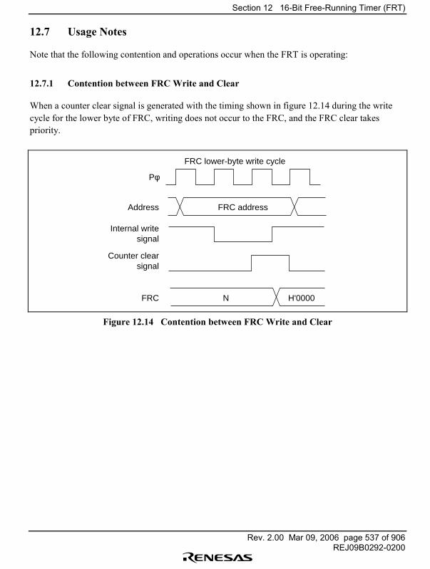
Section 12 16-Bit Free-Running Timer (FRT)
Rev. 2.00 Mar 09, 2006 page 537 of 906REJ09B0292-0200
12.7 Usage Notes
Note that the following contention and operations occur when the FRT is operating:
12.7.1 Contention between FRC Write and Clear
When a counter clear signal is generated with the timing shown in figure 12.14 during the writecycle for the lower byte of FRC, writing does not occur to the FRC, and the FRC clear takespriority.
Pφ
FRC lower-byte write cycle
Address
Internal writesignal
Counter clearsignal
FRC
FRC address
N H'0000
Figure 12.14 Contention between FRC Write and Clear
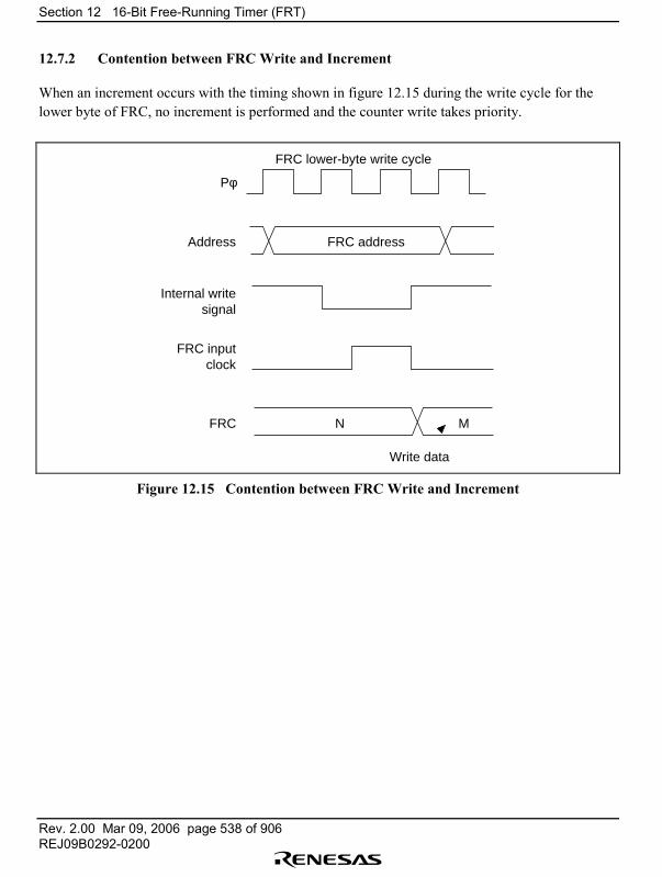
Section 12 16-Bit Free-Running Timer (FRT)
Rev. 2.00 Mar 09, 2006 page 538 of 906REJ09B0292-0200
12.7.2 Contention between FRC Write and Increment
When an increment occurs with the timing shown in figure 12.15 during the write cycle for thelower byte of FRC, no increment is performed and the counter write takes priority.
FRC
FRC address
N M
Write data
Pφ
FRC lower-byte write cycle
Address
Internal writesignal
FRC inputclock
Figure 12.15 Contention between FRC Write and Increment
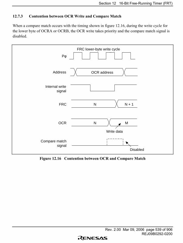
Section 12 16-Bit Free-Running Timer (FRT)
Rev. 2.00 Mar 09, 2006 page 539 of 906REJ09B0292-0200
12.7.3 Contention between OCR Write and Compare Match
When a compare match occurs with the timing shown in figure 12.16, during the write cycle forthe lower byte of OCRA or OCRB, the OCR write takes priority and the compare match signal isdisabled.
FRC
Compare matchsignal
OCR
OCR address
N M
N N + 1
Write data
Disabled
Pφ
FRC lower-byte write cycle
Address
Internal writesignal
Figure 12.16 Contention between OCR and Compare Match
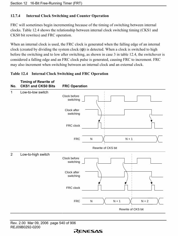
Section 12 16-Bit Free-Running Timer (FRT)
Rev. 2.00 Mar 09, 2006 page 540 of 906REJ09B0292-0200
12.7.4 Internal Clock Switching and Counter Operation
FRC will sometimes begin incrementing because of the timing of switching between internalclocks. Table 12.4 shows the relationship between internal clock switching timing (CKS1 andCKS0 bit rewrites) and FRC operation.
When an internal clock is used, the FRC clock is generated when the falling edge of an internalclock (created by dividing the system clock (φ)) is detected. When a clock is switched to highbefore the switching and to low after switching, as shown in case 3 in table 12.4, the switchover isconsidered a falling edge and an FRC clock pulse is generated, causing FRC to increment. FRCmay also increment when switching between an internal clock and an external clock.
Table 12.4 Internal Clock Switching and FRC Operation
No.Timing of Rewrite ofCKS1 and CKS0 Bits FRC Operation
1 Low-to-low switchClock before
switching
Clock after switching
FRC clock
FRC N N + 1
Rewrite of CKS bit
2 Low-to-high switch
N N + 1 N + 2
Clock before switching
Clock after switching
FRC clock
FRC
Rewrite of CKS bit
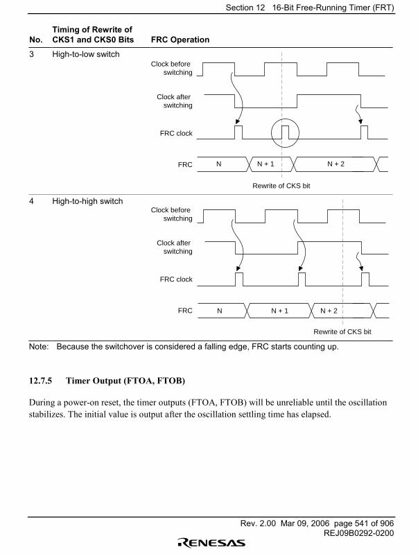
Section 12 16-Bit Free-Running Timer (FRT)
Rev. 2.00 Mar 09, 2006 page 541 of 906REJ09B0292-0200
No.Timing of Rewrite ofCKS1 and CKS0 Bits FRC Operation
3 High-to-low switch
N N + 1 N + 2
Clock before switching
Clock after switching
FRC clock
FRC
Rewrite of CKS bit
4 High-to-high switch
N N + 1 N + 2
Clock before switching
Clock after switching
FRC clock
FRC
Rewrite of CKS bit
Note: Because the switchover is considered a falling edge, FRC starts counting up.
12.7.5 Timer Output (FTOA, FTOB)
During a power-on reset, the timer outputs (FTOA, FTOB) will be unreliable until the oscillationstabilizes. The initial value is output after the oscillation settling time has elapsed.
Section 12 16-Bit Free-Running Timer (FRT)
Rev. 2.00 Mar 09, 2006 page 542 of 906REJ09B0292-0200
Section 13 Watchdog Timer (WDT)
Rev. 2.00 Mar 09, 2006 page 543 of 906REJ09B0292-0200
Section 13 Watchdog Timer (WDT)
13.1 Overview
A single-channel watchdog timer (WDT) is provided on-chip for monitoring system operations. Ifa system becomes uncontrolled and the timer counter overflows without being rewritten correctlyby the CPU, an overflow signal (WDTOVF) is output externally. The WDT can simultaneouslygenerate an internal reset signal for the entire chip.
When this watchdog function is not needed, the WDT can be used as an interval timer. In theinterval timer operation, an interval timer interrupt is generated at each counter overflow. TheWDT is also used when recovering from standby mode, in modifying a clock frequency, and inclock pause mode.
13.1.1 Features
The WDT includes the following features.
• Can be switched between watchdog timer mode and interval timer mode.• WDTOVF output in watchdog timer mode
The WDTOVF signal is output externally when the counter overflows, and a simultaneousinternal reset of the chip can also be selected (either a power-on reset or manual reset can bespecified).
• Interrupt generation in interval timer modeAn interval timer interrupt is generated when the counter overflows.
• Used when standby mode is cleared or the clock frequency is changed, and in clock pausemode.
• Choice of eight counter input clocks
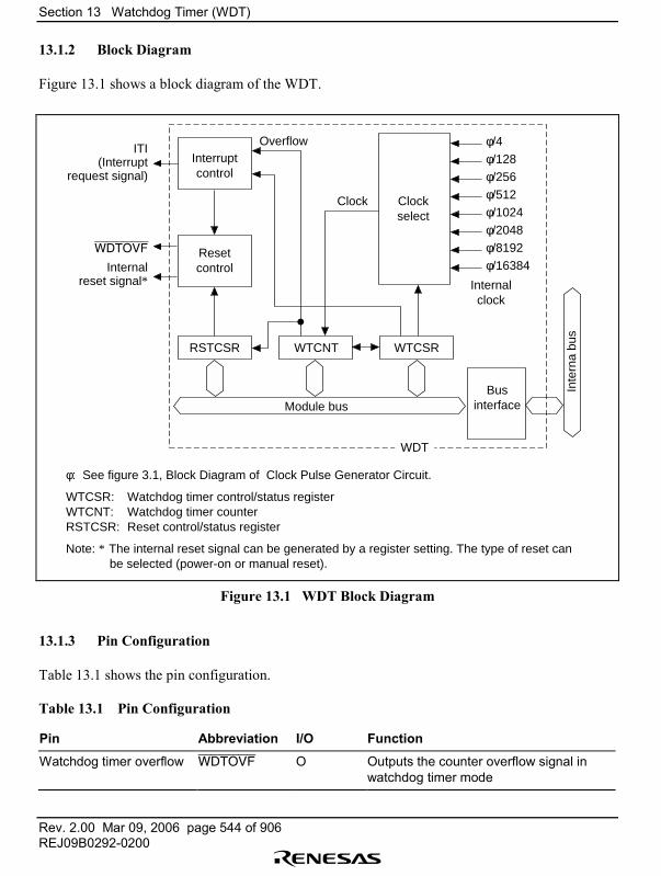
Section 13 Watchdog Timer (WDT)
Rev. 2.00 Mar 09, 2006 page 544 of 906REJ09B0292-0200
13.1.2 Block Diagram
Figure 13.1 shows a block diagram of the WDT.
φ/4φ/128φ/256φ/512φ/1024φ/2048φ/8192φ/16384
Internalclock
Clock
Overflow
Clockselect
Interruptcontrol
Resetcontrol
RSTCSR WTCNT WTCSR
Module busBus
interface
Inte
rna
bus
ITI(Interrupt
request signal)
WDTOVF
Internalreset signal*
WDT
φ: See figure 3.1, Block Diagram of Clock Pulse Generator Circuit.
WTCSR: Watchdog timer control/status registerWTCNT: Watchdog timer counterRSTCSR: Reset control/status register
Note: * The internal reset signal can be generated by a register setting. The type of reset can be selected (power-on or manual reset).
Figure 13.1 WDT Block Diagram
13.1.3 Pin Configuration
Table 13.1 shows the pin configuration.
Table 13.1 Pin Configuration
Pin Abbreviation I/O Function
Watchdog timer overflow WDTOVF O Outputs the counter overflow signal inwatchdog timer mode
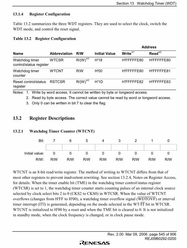
Section 13 Watchdog Timer (WDT)
Rev. 2.00 Mar 09, 2006 page 545 of 906REJ09B0292-0200
13.1.4 Register Configuration
Table 13.2 summarizes the three WDT registers. They are used to select the clock, switch theWDT mode, and control the reset signal.
Table 13.2 Register Configuration
Address
Name Abbreviation R/W Initial Value Write*1 Read*2
Watchdog timercontrol/status register
WTCSR R/(W)*3 H'18 H'FFFFFE80 H'FFFFFE80
Watchdog timercounter
WTCNT R/W H'00 H'FFFFFE80 H'FFFFFE81
Reset control/statusregister
RSTCSR R/(W)*3 H'1D H'FFFFFE82 H'FFFFFE83
Notes: 1. Write by word access. It cannot be written by byte or longword access.2. Read by byte access. The correct value cannot be read by word or longword access.3. Only 0 can be written in bit 7 to clear the flag.
13.2 Register Descriptions
13.2.1 Watchdog Timer Counter (WTCNT)
Bit: 7 6 5 4 3 2 1 0
Initial value: 0 0 0 0 0 0 0 0
R/W: R/W R/W R/W R/W R/W R/W R/W R/W
WTCNT is an 8-bit read/write register. The method of writing to WTCNT differs from that ofmost other registers to prevent inadvertent rewriting. See section 13.2.4, Notes on Register Access,for details. When the timer enable bit (TME) in the watchdog timer control/status register(WTCSR) is set to 1, the watchdog timer counter starts counting pulses of an internal clock sourceselected by clock select bits 2 to 0 (CKS2 to CKS0) in WTCSR. When the value of WTCNToverflows (changes from H'FF to H'00), a watchdog timer overflow signal (WDTOVF) or intervaltimer interrupt (ITI) is generated, depending on the mode selected in the WT/IT bit in WTCSR.WTCNT is initialized to H'00 by a reset and when the TME bit is cleared to 0. It is not initializedin standby mode, when the clock frequency is changed, or in clock pause mode.
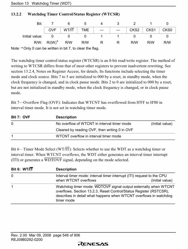
Section 13 Watchdog Timer (WDT)
Rev. 2.00 Mar 09, 2006 page 546 of 906REJ09B0292-0200
13.2.2 Watchdog Timer Control/Status Register (WTCSR)
Bit: 7 6 5 4 3 2 1 0
OVF WT/IT TME � � CKS2 CKS1 CKS0
Initial value: 0 0 0 1 1 0 0 0
R/W: R/(W)* R/W R/W R R R/W R/W R/WNote: * Only 0 can be written in bit 7, to clear the flag.
The watchdog timer control/status register (WTCSR) is an 8-bit read/write register. The method ofwriting to WTCSR differs from that of most other registers to prevent inadvertent rewriting. Seesection 13.2.4, Notes on Register Access, for details. Its functions include selecting the timermode and clock source. Bits 7 to 5 are initialized to 000 by a reset, in standby mode, when theclock frequency is changed, and in clock pause mode. Bits 2 to 0 are initialized to 000 by a reset,but are not initialized in standby mode, when the clock frequency is changed, or in clock pausemode.
Bit 7�Overflow Flag (OVF): Indicates that WTCNT has overflowed from H'FF to H'00 ininterval timer mode. It is not set in watchdog timer mode.
Bit 7: OVF Description
0 No overflow of WTCNT in interval timer mode (Initial value)
Cleared by reading OVF, then writing 0 in OVF
1 WTCNT overflow in interval timer mode
Bit 6�Timer Mode Select (WT/IT): Selects whether to use the WDT as a watchdog timer orinterval timer. When WTCNT overflows, the WDT either generates an interval timer interrupt(ITI) or generates a WDTOVF signal, depending on the mode selected.
Bit 6: WT/ITITITIT Description
0 Interval timer mode: interval timer interrupt (ITI) request to the CPUwhen WTCNT overflows (Initial value)
1 Watchdog timer mode: WDTOVF signal output externally when WTCNToverflows. Section 13.2.3, Reset Control/Status Register (RSTCSR),describes in detail what happens when WTCNT overflows in watchdogtimer mode
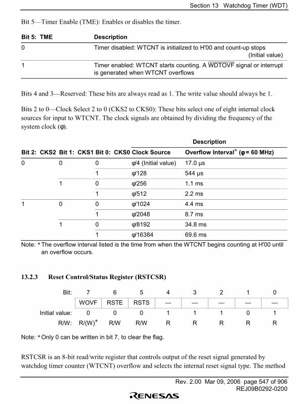
Section 13 Watchdog Timer (WDT)
Rev. 2.00 Mar 09, 2006 page 547 of 906REJ09B0292-0200
Bit 5�Timer Enable (TME): Enables or disables the timer.
Bit 5: TME Description
0 Timer disabled: WTCNT is initialized to H'00 and count-up stops(Initial value)
1 Timer enabled: WTCNT starts counting. A WDTOVF signal or interruptis generated when WTCNT overflows
Bits 4 and 3�Reserved: These bits are always read as 1. The write value should always be 1.
Bits 2 to 0�Clock Select 2 to 0 (CKS2 to CKS0): These bits select one of eight internal clocksources for input to WTCNT. The clock signals are obtained by dividing the frequency of thesystem clock (φ).
Description
Bit 2: CKS2 Bit 1: CKS1 Bit 0: CKS0 Clock Source Overflow Interval* (φφφφ = 60 MHz)
0 0 0 φ/4 (Initial value) 17.0 µs
1 φ/128 544 µs
1 0 φ/256 1.1 ms
1 φ/512 2.2 ms
1 0 0 φ/1024 4.4 ms
1 φ/2048 8.7 ms
1 0 φ/8192 34.8 ms
1 φ/16384 69.6 msNote: * The overflow interval listed is the time from when the WTCNT begins counting at H'00 until
an overflow occurs.
13.2.3 Reset Control/Status Register (RSTCSR)
Bit: 7 6 5 4 3 2 1 0
WOVF RSTE RSTS � � � � �
Initial value: 0 0 0 1 1 1 0 1
R/W: R/(W)* R/W R/W R R R R R
Note: * Only 0 can be written in bit 7, to clear the flag.
RSTCSR is an 8-bit read/write register that controls output of the reset signal generated bywatchdog timer counter (WTCNT) overflow and selects the internal reset signal type. The method
Section 13 Watchdog Timer (WDT)
Rev. 2.00 Mar 09, 2006 page 548 of 906REJ09B0292-0200
of writing to RSTCSR differs from that of most other registers to prevent inadvertent rewriting.See section 13.2.4, Notes on Register Access, for details. RSTCR is initialized to H'1D by input ofa reset signal from the RES pin, but is not initialized by the internal reset signal generated byoverflow of the WDT. It is initialized to H'1D in standby mode, when the clock frequency ischanged, and in clock pause mode.
Bit 7�Watchdog Timer Overflow Flag (WOVF): Indicates that WTCNT has overflowed (fromH'FF to H'00) in watchdog timer mode. It is not set in interval timer mode.
Bit 7: WOVF Description
0 No WTCNT overflow in watchdog timer mode (Initial value)
Cleared by reading WOVF, then writing 0 in WOVF
1 Set by WTCNT overflow in watchdog timer mode
Bit 6�Reset Enable (RSTE): Selects whether to reset the chip internally if WTCNT overflows inwatchdog timer mode.
Bit 6: RSTE Description
0 Not reset when WTCNT overflows (Initial value)
LSI not reset internally, but WTCNT and WTCSR reset within WDT
1 Reset when WTCNT overflows
Bit 5�Reset Select (RSTS): Selects the type of internal reset generated if WTCNT overflows inwatchdog timer mode.
Bit 5: RSTS Description
0 Power-on reset (Initial value)
1 Manual reset
Bits 4 to 2, bit 0�Reserved: These bits are always read as 1. The write value should always be 1.
Bit 1� Reserved: This bit is always read as 0. The write value should always be 0.
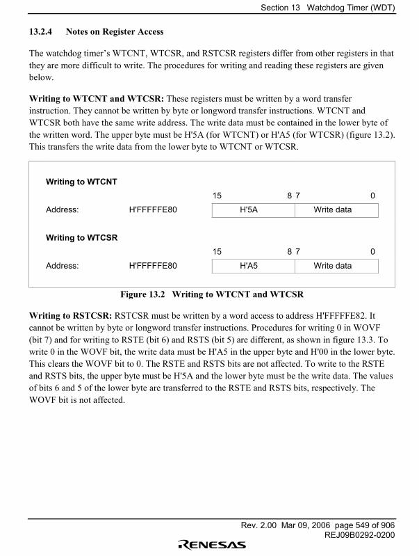
Section 13 Watchdog Timer (WDT)
Rev. 2.00 Mar 09, 2006 page 549 of 906REJ09B0292-0200
13.2.4 Notes on Register Access
The watchdog timer�s WTCNT, WTCSR, and RSTCSR registers differ from other registers in thatthey are more difficult to write. The procedures for writing and reading these registers are givenbelow.
Writing to WTCNT and WTCSR: These registers must be written by a word transferinstruction. They cannot be written by byte or longword transfer instructions. WTCNT andWTCSR both have the same write address. The write data must be contained in the lower byte ofthe written word. The upper byte must be H'5A (for WTCNT) or H'A5 (for WTCSR) (figure 13.2).This transfers the write data from the lower byte to WTCNT or WTCSR.
Writing to WTCNT15 8 7 0
Address: H'FFFFFE80 H'5A Write data
Writing to WTCSR15 8 7 0
Address: H'FFFFFE80 H'A5 Write data
Figure 13.2 Writing to WTCNT and WTCSR
Writing to RSTCSR: RSTCSR must be written by a word access to address H'FFFFFE82. Itcannot be written by byte or longword transfer instructions. Procedures for writing 0 in WOVF(bit 7) and for writing to RSTE (bit 6) and RSTS (bit 5) are different, as shown in figure 13.3. Towrite 0 in the WOVF bit, the write data must be H'A5 in the upper byte and H'00 in the lower byte.This clears the WOVF bit to 0. The RSTE and RSTS bits are not affected. To write to the RSTEand RSTS bits, the upper byte must be H'5A and the lower byte must be the write data. The valuesof bits 6 and 5 of the lower byte are transferred to the RSTE and RSTS bits, respectively. TheWOVF bit is not affected.
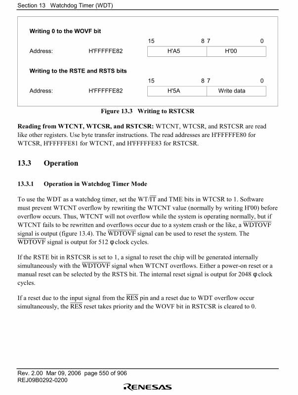
Section 13 Watchdog Timer (WDT)
Rev. 2.00 Mar 09, 2006 page 550 of 906REJ09B0292-0200
Writing 0 to the WOVF bit15 8 7 0
Address: H'FFFFFE82 H'A5 H'00
Writing to the RSTE and RSTS bits15 8 7 0
Address: H'FFFFFE82 H'5A Write data
Figure 13.3 Writing to RSTCSR
Reading from WTCNT, WTCSR, and RSTCSR: WTCNT, WTCSR, and RSTCSR are readlike other registers. Use byte transfer instructions. The read addresses are H'FFFFFE80 forWTCSR, H'FFFFFE81 for WTCNT, and H'FFFFFE83 for RSTCSR.
13.3 Operation
13.3.1 Operation in Watchdog Timer Mode
To use the WDT as a watchdog timer, set the WT/IT and TME bits in WTCSR to 1. Softwaremust prevent WTCNT overflow by rewriting the WTCNT value (normally by writing H'00) beforeoverflow occurs. Thus, WTCNT will not overflow while the system is operating normally, but ifWTCNT fails to be rewritten and overflows occur due to a system crash or the like, a WDTOVFsignal is output (figure 13.4). The WDTOVF signal can be used to reset the system. TheWDTOVF signal is output for 512 φ clock cycles.
If the RSTE bit in RSTCSR is set to 1, a signal to reset the chip will be generated internallysimultaneously with the WDTOVF signal when WTCNT overflows. Either a power-on reset or amanual reset can be selected by the RSTS bit. The internal reset signal is output for 2048 φ clockcycles.
If a reset due to the input signal from the RES pin and a reset due to WDT overflow occursimultaneously, the RES reset takes priority and the WOVF bit in RSTCSR is cleared to 0.
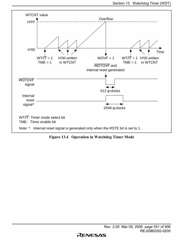
Section 13 Watchdog Timer (WDT)
Rev. 2.00 Mar 09, 2006 page 551 of 906REJ09B0292-0200
WOVF = 1
WTCNT valueOverflow
WT/IT = 1TME = 1
WT/IT = 1TME = 1
H'00 writtenin WTCNT
H'00 writtenin WTCNT
WDTOVF andinternal reset generated
H'FF
H'00
512 φ clocks
2048 φ clocks
WDTOVF
signal
Internalreset
signal*
Time
WT/IT: Timer mode select bitTME: Timer enable bit
Note: * Internal reset signal is generated only when the RSTE bit is set to 1.
Figure 13.4 Operation in Watchdog Timer Mode
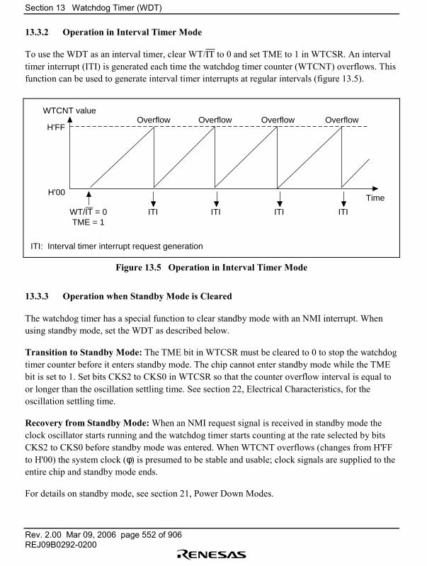
Section 13 Watchdog Timer (WDT)
Rev. 2.00 Mar 09, 2006 page 552 of 906REJ09B0292-0200
13.3.2 Operation in Interval Timer Mode
To use the WDT as an interval timer, clear WT/IT to 0 and set TME to 1 in WTCSR. An intervaltimer interrupt (ITI) is generated each time the watchdog timer counter (WTCNT) overflows. Thisfunction can be used to generate interval timer interrupts at regular intervals (figure 13.5).
ITIITIITIITI
WTCNT valueOverflow Overflow Overflow Overflow
WT/IT = 0TME = 1
H'FF
H'00Time
ITI: Interval timer interrupt request generation
Figure 13.5 Operation in Interval Timer Mode
13.3.3 Operation when Standby Mode is Cleared
The watchdog timer has a special function to clear standby mode with an NMI interrupt. Whenusing standby mode, set the WDT as described below.
Transition to Standby Mode: The TME bit in WTCSR must be cleared to 0 to stop the watchdogtimer counter before it enters standby mode. The chip cannot enter standby mode while the TMEbit is set to 1. Set bits CKS2 to CKS0 in WTCSR so that the counter overflow interval is equal toor longer than the oscillation settling time. See section 22, Electrical Characteristics, for theoscillation settling time.
Recovery from Standby Mode: When an NMI request signal is received in standby mode theclock oscillator starts running and the watchdog timer starts counting at the rate selected by bitsCKS2 to CKS0 before standby mode was entered. When WTCNT overflows (changes from H'FFto H'00) the system clock (φ) is presumed to be stable and usable; clock signals are supplied to theentire chip and standby mode ends.
For details on standby mode, see section 21, Power Down Modes.
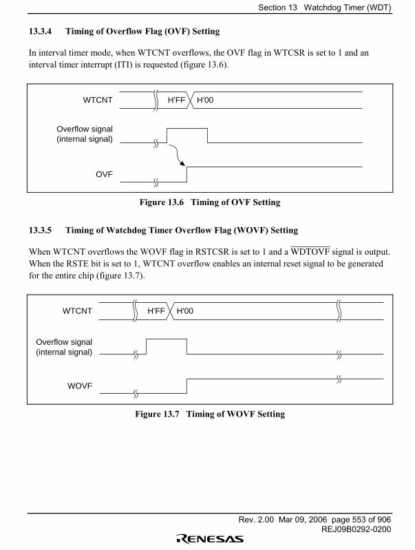
Section 13 Watchdog Timer (WDT)
Rev. 2.00 Mar 09, 2006 page 553 of 906REJ09B0292-0200
13.3.4 Timing of Overflow Flag (OVF) Setting
In interval timer mode, when WTCNT overflows, the OVF flag in WTCSR is set to 1 and aninterval timer interrupt (ITI) is requested (figure 13.6).
WTCNT H'FF H'00
Overflow signal(internal signal)
OVF
Figure 13.6 Timing of OVF Setting
13.3.5 Timing of Watchdog Timer Overflow Flag (WOVF) Setting
When WTCNT overflows the WOVF flag in RSTCSR is set to 1 and a WDTOVF signal is output.When the RSTE bit is set to 1, WTCNT overflow enables an internal reset signal to be generatedfor the entire chip (figure 13.7).
WTCNT H'FF H'00
Overflow signal(internal signal)
WOVF
Figure 13.7 Timing of WOVF Setting

Section 13 Watchdog Timer (WDT)
Rev. 2.00 Mar 09, 2006 page 554 of 906REJ09B0292-0200
13.4 Usage Notes
13.4.1 Contention between WTCNT Write and Increment
If a count-up pulse is generated at the timing shown in figure 13.8 during a watchdog timercounter (WTCNT) write cycle, the write takes priority and the timer counter is not incremented(figure 13.8).
WTCNT addressAddress
Internal writesignal
WTCNT inputclock
WTCNT
Counter write data
N M
Figure 13.8 Contention between WTCNT Write and Increment
13.4.2 Changing CKS2 to CKS0 Bit Values
If the values of bits CKS2 to CKS0 are altered while the WDT is running, the count mayincrement incorrectly. Always stop the watchdog timer (by clearing the TME bit to 0) beforechanging the values of bits CKS2 to CKS0.
13.4.3 Switching between Watchdog Timer Mode and Interval Timer Mode
The WDT may not operate correctly if it is switched between watchdog timer mode and intervaltimer mode while it is running.
To ensure correct operation, always stop the watchdog timer (by clearing the TME bit to 0) beforeswitching between watchdog timer mode and interval timer mode.
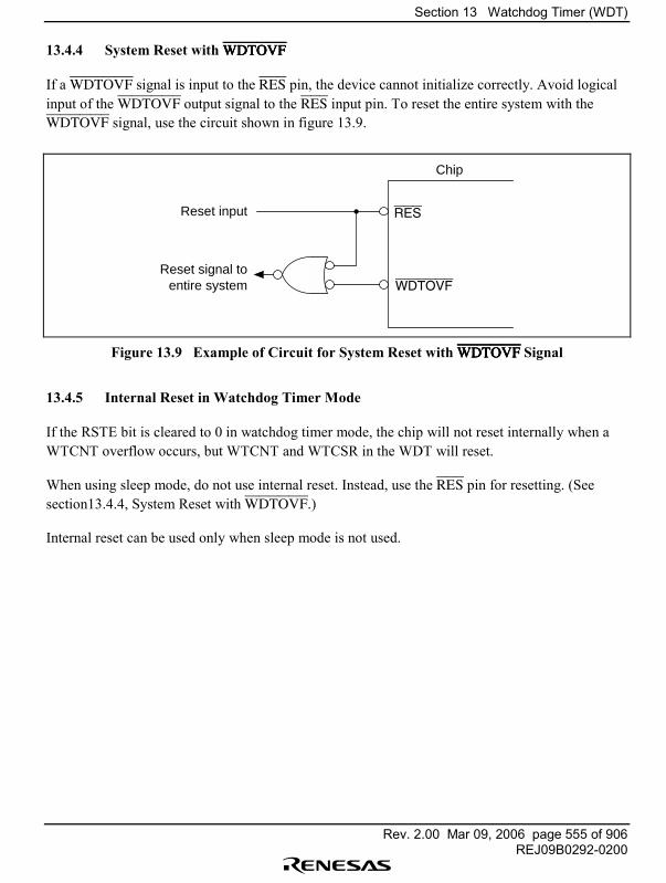
Section 13 Watchdog Timer (WDT)
Rev. 2.00 Mar 09, 2006 page 555 of 906REJ09B0292-0200
13.4.4 System Reset with WDTOVFWDTOVFWDTOVFWDTOVF
If a WDTOVF signal is input to the RES pin, the device cannot initialize correctly. Avoid logicalinput of the WDTOVF output signal to the RES input pin. To reset the entire system with theWDTOVF signal, use the circuit shown in figure 13.9.
Reset input
Reset signal toentire system
Chip
RES
WDTOVF
Figure 13.9 Example of Circuit for System Reset with WDTOVFWDTOVFWDTOVFWDTOVF Signal
13.4.5 Internal Reset in Watchdog Timer Mode
If the RSTE bit is cleared to 0 in watchdog timer mode, the chip will not reset internally when aWTCNT overflow occurs, but WTCNT and WTCSR in the WDT will reset.
When using sleep mode, do not use internal reset. Instead, use the RES pin for resetting. (Seesection13.4.4, System Reset with WDTOVF.)
Internal reset can be used only when sleep mode is not used.

Section 13 Watchdog Timer (WDT)
Rev. 2.00 Mar 09, 2006 page 556 of 906REJ09B0292-0200
Section 14 Serial Communication Interface with FIFO (SCIF)
Rev. 2.00 Mar 09, 2006 page 557 of 906REJ09B0292-0200
Section 14 Serial Communication Interface with FIFO(SCIF)
14.1 Overview
The SH7616 is equipped with a two-channel serial communication interface with built-in FIFObuffers (SCIF: SCI with FIFO). The SCIF can handle both asynchronous and synchronous serialcommunication. A function is also provided for serial communication between processors(multiprocessor communication function).
An on-chip Infrared Data Association (IrDA) interface based on the IrDA 1.0 system is alsoprovided, enabling infrared communication.
Sixteen-stage FIFO registers are provided for both transmission and reception, enabling fast,efficient, and continuous communication.
14.1.1 Features
The SCIF has the following features:
• Choice of synchronous or asynchronous serial communication mode Asynchronous mode
Serial data communication is executed using an asynchronous system in whichsynchronization is achieved character by character. Serial data communication can becarried out with standard asynchronous communication chips such as a UniversalAsynchronous Receiver/Transmitter (UART) or Asynchronous Communication InterfaceAdapter (ACIA). A multiprocessor communication function is also provided that enablesserial data communication with a number of processors.There is a choice of 12 serial data communication formats.• Data length: 7 or 8• Stop bit length: 1 or 2 bits• Parity: Even/odd/none• Multiprocessor bit: 1 or 0• Receive error detection: Parity, overrun, and framing errors• Automatic break detection
Section 14 Serial Communication Interface with FIFO (SCIF)
Rev. 2.00 Mar 09, 2006 page 558 of 906REJ09B0292-0200
Synchronous modeSerial data communication is synchronized with a clock. Serial data communication can becarried out with other chips that have a synchronous communication function.There is a single serial data communication format.• Data length: 8 bits• Receive error detection: Overrun errors
• IrDA 1.0 compliance• Full-duplex communication capability
The transmitter and receiver are mutually independent, enabling transmission and reception tobe executed simultaneously. In addition, the transmitter and receiver both have a 16-stageFIFO buffer structure, enabling continuous serial data transmission and reception.(However, IrDA communication is carried out in half-duplex mode.)
• Built-in baud rate generator allows a choice of bit rates.• Choice of transmit/receive clock source: internal clock from baud rate generator or external
clock from SCK pin• Four interrupt sources
There are four interrupt sources�transmit-FIFO-data-empty, break, receive-FIFO-data-full,and receive-error�that can issue requests independently. The transmit-FIFO-data-empty andreceive-FIFO-data-full interrupts can activate the on-chip DMAC to execute data transfer.
• When not in use, the SCIF can be stopped by halting its clock supply to reduce powerconsumption.
• Choice of LSB-first or MSB-first mode• In asynchronous mode, operation can be selected on a base clock of 4, 8, or 16 times the bit
rate.• Built-in modem control functions (RTS and CTS)

Section 14 Serial Communication Interface with FIFO (SCIF)
Rev. 2.00 Mar 09, 2006 page 559 of 906REJ09B0292-0200
14.1.2 Block Diagrams
A block diagram of the SCIF is shown in figure 14.1, and a diagram of the IrDA block in figure14.2.
Module data bus
SCFRDR (16-stage)
SCFTDR(16-stage)
SCRSRRxD
TxD
SCK
SCTSR
SCFDR
SCFCR
SC1SSRSC2SSRSCSCR
SCSMRSCFERSCIMR
SCBRR
Parity generation
Parity check
Transmission/reception control
Baud rategenerator
Clock
External clock
Pφ
Pφ/4
Pφ/16
Pφ/64
BRI
IrDA/SCI switchover (to IrDA block)
TxIRxIERI
SCIF
LegendSCRSR: Receive shift registerSCFRDR: Receive FIFO data registerSCTSR: Transmit shift registerSCFTDR: Transmit FIFO data registerSCSMR: Serial mode registerSCSCR: Serial control register
Bus
inte
rfac
e
Internal data bus
SC1SSR: Serial status 1 registerSC2SSR: Serial status 2 registerSCBRR: Bit rate registerSCFCR: FIFO control registerSCFDR: FIFO data count registerSCFER: FIFO error registerSCIMR: IrDA mode register
Figure 14.1 Block Diagram of SCIF
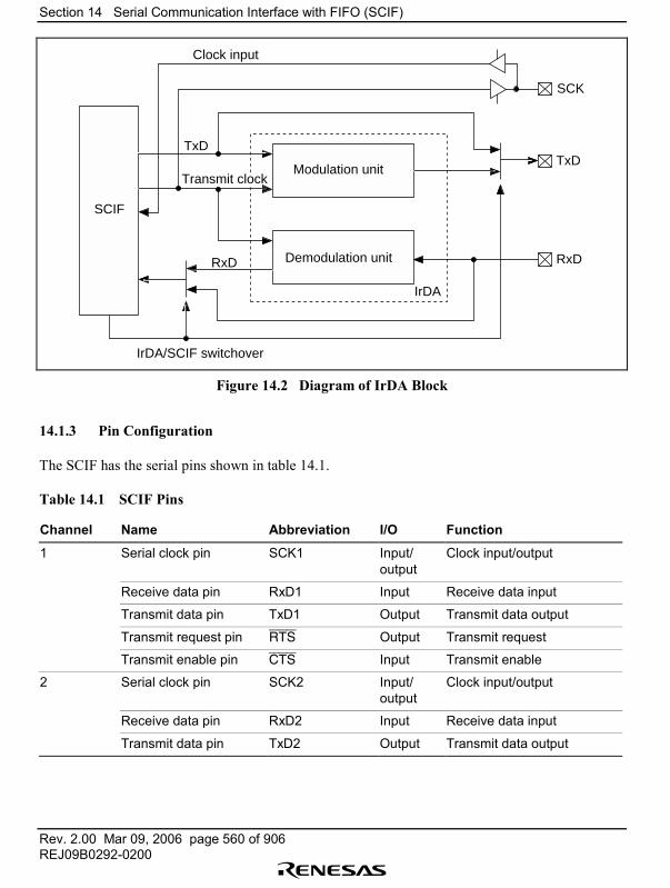
Section 14 Serial Communication Interface with FIFO (SCIF)
Rev. 2.00 Mar 09, 2006 page 560 of 906REJ09B0292-0200
SCIF
IrDA/SCIF switchover
SCK
IrDA
TxDTxD
RxD RxDDemodulation unit
Modulation unit
Clock input
Transmit clock
Figure 14.2 Diagram of IrDA Block
14.1.3 Pin Configuration
The SCIF has the serial pins shown in table 14.1.
Table 14.1 SCIF Pins
Channel Name Abbreviation I/O Function
1 Serial clock pin SCK1 Input/output
Clock input/output
Receive data pin RxD1 Input Receive data input
Transmit data pin TxD1 Output Transmit data output
Transmit request pin RTS Output Transmit request
Transmit enable pin CTS Input Transmit enable
2 Serial clock pin SCK2 Input/output
Clock input/output
Receive data pin RxD2 Input Receive data input
Transmit data pin TxD2 Output Transmit data output
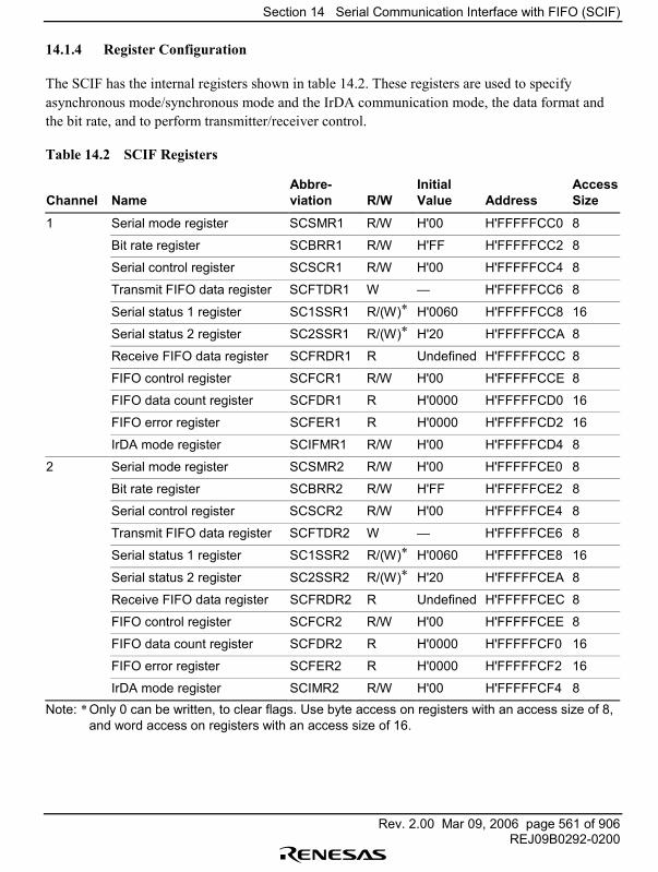
Section 14 Serial Communication Interface with FIFO (SCIF)
Rev. 2.00 Mar 09, 2006 page 561 of 906REJ09B0292-0200
14.1.4 Register Configuration
The SCIF has the internal registers shown in table 14.2. These registers are used to specifyasynchronous mode/synchronous mode and the IrDA communication mode, the data format andthe bit rate, and to perform transmitter/receiver control.
Table 14.2 SCIF Registers
Channel
Name
Abbre-viation
R/W
InitialValue
Address
AccessSize
1 Serial mode register SCSMR1 R/W H'00 H'FFFFFCC0 8
Bit rate register SCBRR1 R/W H'FF H'FFFFFCC2 8
Serial control register SCSCR1 R/W H'00 H'FFFFFCC4 8
Transmit FIFO data register SCFTDR1 W � H'FFFFFCC6 8
Serial status 1 register SC1SSR1 R/(W)* H'0060 H'FFFFFCC8 16
Serial status 2 register SC2SSR1 R/(W)* H'20 H'FFFFFCCA 8
Receive FIFO data register SCFRDR1 R Undefined H'FFFFFCCC 8
FIFO control register SCFCR1 R/W H'00 H'FFFFFCCE 8
FIFO data count register SCFDR1 R H'0000 H'FFFFFCD0 16
FIFO error register SCFER1 R H'0000 H'FFFFFCD2 16
IrDA mode register SCIFMR1 R/W H'00 H'FFFFFCD4 8
2 Serial mode register SCSMR2 R/W H'00 H'FFFFFCE0 8
Bit rate register SCBRR2 R/W H'FF H'FFFFFCE2 8
Serial control register SCSCR2 R/W H'00 H'FFFFFCE4 8
Transmit FIFO data register SCFTDR2 W � H'FFFFFCE6 8
Serial status 1 register SC1SSR2 R/(W)* H'0060 H'FFFFFCE8 16
Serial status 2 register SC2SSR2 R/(W)* H'20 H'FFFFFCEA 8
Receive FIFO data register SCFRDR2 R Undefined H'FFFFFCEC 8
FIFO control register SCFCR2 R/W H'00 H'FFFFFCEE 8
FIFO data count register SCFDR2 R H'0000 H'FFFFFCF0 16
FIFO error register SCFER2 R H'0000 H'FFFFFCF2 16
IrDA mode register SCIMR2 R/W H'00 H'FFFFFCF4 8Note: * Only 0 can be written, to clear flags. Use byte access on registers with an access size of 8,
and word access on registers with an access size of 16.

Section 14 Serial Communication Interface with FIFO (SCIF)
Rev. 2.00 Mar 09, 2006 page 562 of 906REJ09B0292-0200
14.2 Register Descriptions
With the exception of the IrDA mode register (SCIMR) and bits 6 to 3 (ICK3 to ICK0) of theserial mode register (SCSMR), IrDA communication mode settings are the same as forasynchronous mode.
14.2.1 Receive Shift Register (SCRSR)
Bit: 7 6 5 4 3 2 1 0
R/W: � � � � � � � �
The receive shift register (SCRSR) is the register used to receive serial data.
The SCIF sets serial data input from the RxD pin in SCRSR in the order received, starting with theLSB (bit 0) or MSB (bit 7), and converts it to parallel data. When one byte of data has beenreceived, it is transferred to the receive FIFO data register (SCFRDR) automatically.
SCRSR cannot be read or written to directly.
14.2.2 Receive FIFO Data Register (SCFRDR)
Bit: 7 6 5 4 3 2 1 0
R/W: R R R R R R R R
The receive FIFO data register (SCFRDR) is a 16-stage FIFO register (8 bits per stage) that storesreceived serial data.
When the SCIF has received one byte of serial data, it transfers the received data from SCRSR toSCFRDR where it is stored, and completes the receive operation. SCRSR is then enabled forreception, and consecutive receive operations can be performed until the receive FIFO dataregister is full (16 data bytes).
SCFRDR is a read-only register, and cannot be written to.
If a read is performed when there is no receive data in the receive FIFO data register, an undefinedvalue will be returned. When the receive FIFO data register is full of receive data, subsequentserial data is lost.
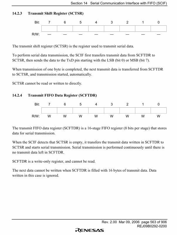
Section 14 Serial Communication Interface with FIFO (SCIF)
Rev. 2.00 Mar 09, 2006 page 563 of 906REJ09B0292-0200
14.2.3 Transmit Shift Register (SCTSR)
Bit: 7 6 5 4 3 2 1 0
R/W: � � � � � � � �
The transmit shift register (SCTSR) is the register used to transmit serial data.
To perform serial data transmission, the SCIF first transfers transmit data from SCFTDR toSCTSR, then sends the data to the TxD pin starting with the LSB (bit 0) or MSB (bit 7).
When transmission of one byte is completed, the next transmit data is transferred from SCFTDRto SCTSR, and transmission started, automatically.
SCTSR cannot be read or written to directly.
14.2.4 Transmit FIFO Data Register (SCFTDR)
Bit: 7 6 5 4 3 2 1 0
R/W: W W W W W W W W
The transmit FIFO data register (SCFTDR) is a 16-stage FIFO register (8 bits per stage) that storesdata for serial transmission.
When the SCIF detects that SCTSR is empty, it transfers the transmit data written in SCFTDR toSCTSR and starts serial transmission. Serial transmission is performed continuously until there isno transmit data left in SCFTDR.
SCFTDR is a write-only register, and cannot be read.
The next data cannot be written when SCFTDR is filled with 16 bytes of transmit data. Datawritten in this case is ignored.
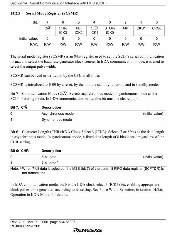
Section 14 Serial Communication Interface with FIFO (SCIF)
Rev. 2.00 Mar 09, 2006 page 564 of 906REJ09B0292-0200
14.2.5 Serial Mode Register (SCSMR)
Bit: 7 6 5 4 3 2 1 0
C/A CHR/ICK3
PE/ICK2
O/E/ICK1
STOP/ICK0
MP CKS1 CKS0
Initial value: 0 0 0 0 0 0 0 0
R/W: R/W R/W R/W R/W R/W R/W R/W R/W
The serial mode register (SCSMR) is an 8-bit register used to set the SCIF�s serial communicationformat and select the baud rate generator clock source. In IrDA communication mode, it is used toselect the output pulse width.
SCSMR can be read or written to by the CPU at all times.
SCSMR is initialized to H'00 by a reset, by the module standby function, and in standby mode.
Bit 7�Communication Mode (C/A): Selects asynchronous mode or synchronous mode as theSCIF operating mode. In IrDA communication mode, this bit must be cleared to 0.
Bit 7: C/AAAA Description
0 Asynchronous mode (Initial value)
1 Synchronous mode
Bit 6�Character Length (CHR)/IrDA Clock Select 3 (ICK3): Selects 7 or 8 bits as the data lengthin asynchronous mode. In synchronous mode, a fixed data length of 8 bits is used regardless of theCHR setting,
Bit 6: CHR Description
0 8-bit data (Initial value)
1 7-bit data*
Note: * When 7-bit data is selected, the MSB (bit 7) of the transmit FIFO data register (SCFTDR) isnot transmitted.
In IrDA communication mode, bit 6 is the IrDA clock select 3 (ICK3) bit, enabling appropriateclock pulses to be generated according to its setting. See Pulse Width Selection, in section 14.3.6,Operation in IrDA Mode, for details.
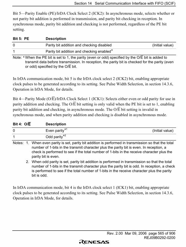
Section 14 Serial Communication Interface with FIFO (SCIF)
Rev. 2.00 Mar 09, 2006 page 565 of 906REJ09B0292-0200
Bit 5�Parity Enable (PE)/IrDA Clock Select 2 (ICK2): In asynchronous mode, selects whether ornot parity bit addition is performed in transmission, and parity bit checking in reception. Insynchronous mode, parity bit addition and checking is not performed, regardless of the PE bitsetting.
Bit 5: PE Description
0 Parity bit addition and checking disabled (Initial value)
1 Parity bit addition and checking enabled*
Note: * When the PE bit is set to 1, the parity (even or odd) specified by the O/E bit is added totransmit data before transmission. In reception, the parity bit is checked for the parity (evenor odd) specified by the O/E bit.
In IrDA communication mode, bit 5 is the IrDA clock select 2 (ICK2) bit, enabling appropriateclock pulses to be generated according to its setting. See Pulse Width Selection, in section 14.3.6,Operation in IrDA Mode, for details.
Bit 4�Parity Mode (O/E)/IrDA Clock Select 1 (ICK1): Selects either even or odd parity for use inparity addition and checking. The O/E bit setting is only valid when the PE bit is set to 1, enablingparity bit addition and checking, in asynchronous mode. The O/E bit setting is invalid insynchronous mode, and when parity addition and checking is disabled in asynchronous mode.
Bit 4: O/EEEE Description
0 Even parity*1 (Initial value)
1 Odd parity*2
Notes: 1. When even parity is set, parity bit addition is performed in transmission so that the totalnumber of 1-bits in the transmit character plus the parity bit is even. In reception, acheck is performed to see if the total number of 1-bits in the receive character plus theparity bit is even.
2. When odd parity is set, parity bit addition is performed in transmission so that the totalnumber of 1-bits in the transmit character plus the parity bit is odd. In reception, a checkis performed to see if the total number of 1-bits in the receive character plus the paritybit is odd.
In IrDA communication mode, bit 4 is the IrDA clock select 1 (ICK1) bit, enabling appropriateclock pulses to be generated according to its setting. See Pulse Width Selection, in section 14.3.6,Operation in IrDA Mode, for details.
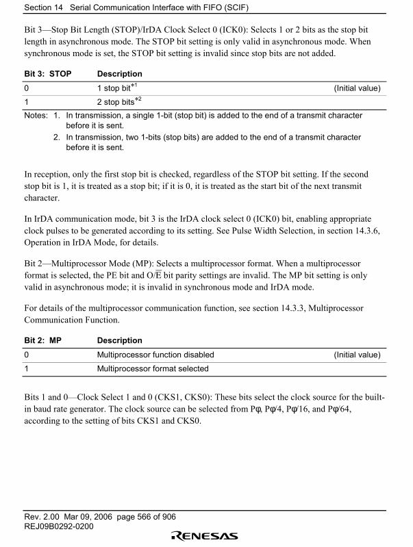
Section 14 Serial Communication Interface with FIFO (SCIF)
Rev. 2.00 Mar 09, 2006 page 566 of 906REJ09B0292-0200
Bit 3�Stop Bit Length (STOP)/IrDA Clock Select 0 (ICK0): Selects 1 or 2 bits as the stop bitlength in asynchronous mode. The STOP bit setting is only valid in asynchronous mode. Whensynchronous mode is set, the STOP bit setting is invalid since stop bits are not added.
Bit 3: STOP Description
0 1 stop bit*1 (Initial value)
1 2 stop bits*2
Notes: 1. In transmission, a single 1-bit (stop bit) is added to the end of a transmit characterbefore it is sent.
2. In transmission, two 1-bits (stop bits) are added to the end of a transmit characterbefore it is sent.
In reception, only the first stop bit is checked, regardless of the STOP bit setting. If the secondstop bit is 1, it is treated as a stop bit; if it is 0, it is treated as the start bit of the next transmitcharacter.
In IrDA communication mode, bit 3 is the IrDA clock select 0 (ICK0) bit, enabling appropriateclock pulses to be generated according to its setting. See Pulse Width Selection, in section 14.3.6,Operation in IrDA Mode, for details.
Bit 2�Multiprocessor Mode (MP): Selects a multiprocessor format. When a multiprocessorformat is selected, the PE bit and O/E bit parity settings are invalid. The MP bit setting is onlyvalid in asynchronous mode; it is invalid in synchronous mode and IrDA mode.
For details of the multiprocessor communication function, see section 14.3.3, MultiprocessorCommunication Function.
Bit 2: MP Description
0 Multiprocessor function disabled (Initial value)
1 Multiprocessor format selected
Bits 1 and 0�Clock Select 1 and 0 (CKS1, CKS0): These bits select the clock source for the built-in baud rate generator. The clock source can be selected from Pφ, Pφ/4, Pφ/16, and Pφ/64,according to the setting of bits CKS1 and CKS0.
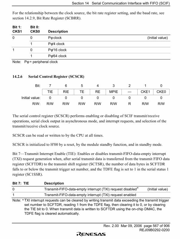
Section 14 Serial Communication Interface with FIFO (SCIF)
Rev. 2.00 Mar 09, 2006 page 567 of 906REJ09B0292-0200
For the relationship between the clock source, the bit rate register setting, and the baud rate, seesection 14.2.9, Bit Rate Register (SCBRR).
Bit 1:CKS1
Bit 0:CKS0 Description
0 0 Pφ clock (Initial value)
1 Pφ/4 clock
1 0 Pφ/16 clock
1 Pφ/64 clockNote: Pφ = peripheral clock
14.2.6 Serial Control Register (SCSCR)
Bit: 7 6 5 4 3 2 1 0
TIE RIE TE RE MPIE � CKE1 CKE0
Initial value: 0 0 0 0 0 0 0 0
R/W: R/W R/W R/W R/W R/W R R/W R/W
The serial control register (SCSCR) performs enabling or disabling of SCIF transmit/receiveoperations, serial clock output in asynchronous mode, and interrupt requests, and selection of thetransmit/receive clock source.
SCSCR can be read or written to by the CPU at all times.
SCSCR is initialized to H'00 by a reset, by the module standby function, and in standby mode.
Bit 7�Transmit Interrupt Enable (TIE): Enables or disables transmit-FIFO-data-empty interrupt(TXI) request generation when, after serial transmit data is transferred from the transmit FIFO dataregister (SCFTDR) to the transmit shift register (SCTSR), the number of data bytes in SCFTDRfalls to or below the transmit trigger set number, and the TDFE flag is set to 1 in the serial status 1register (SC1SSR).
Bit 7: TIE Description0 Transmit-FIFO-data-empty interrupt (TXI) request disabled* (Initial value)1 Transmit-FIFO-data-empty interrupt (TXI) request enabledNote: * TXI interrupt requests can be cleared by writing transmit data exceeding the transmit trigger
set number to SCFTDR, reading 1 from the TDFE flag, then clearing it to 0, or by clearingthe TIE bit to 0. When transmit data is written to SCFTDR using the on-chip DMAC, theTDFE flag is cleared automatically.
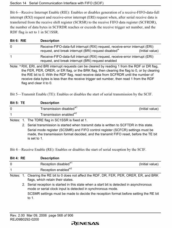
Section 14 Serial Communication Interface with FIFO (SCIF)
Rev. 2.00 Mar 09, 2006 page 568 of 906REJ09B0292-0200
Bit 6�Receive Interrupt Enable (RIE): Enables or disables generation of a receive-FIFO-data-fullinterrupt (RXI) request and receive-error interrupt (ERI) request when, after serial receive data istransferred from the receive shift register (SCRSR) to the receive FIFO data register (SCFRDR),the number of data bytes in SCFRDR reaches or exceeds the receive trigger set number, and theRDF flag is set to 1 in SC1SSR.
Bit 6: RIE Description
0 Receive-FIFO-data-full interrupt (RXI) request, receive-error interrupt (ERI)request, and break interrupt (BRI) request disabled* (Initial value)
1 Receive-FIFO-data-full interrupt (RXI) request, receive-error interrupt (ERI)request, and break interrupt (BRI) request enabled
Note: * RXI, ERI, and BRI interrupt requests can be cleared by reading 1 from the RDF or DR flag,the FER, PER, ORER, or ER flag, or the BRK flag, then clearing the flag to 0, or by clearingthe RIE bit to 0. With the RDF flag, read receive data from SCFRDR until the number ofreceive data bytes is less than the receive trigger set number, then read 1 from the RDFflag and clear it to 0.
Bit 5�Transmit Enable (TE): Enables or disables the start of serial transmission by the SCIF.
Bit 5: TE Description
0 Transmission disabled*1 (Initial value)
1 Transmission enabled*2
Notes: 1. The TDRE flag in SC1SSR is fixed at 1.2. Serial transmission is started when transmit data is written to SCFTDR in this state.
Serial mode register (SCSMR) and FIFO control register (SCFCR) settings must bemade, the transmission format decided, and the transmit FIFO reset, before the TE bitis set to 1.
Bit 4�Receive Enable (RE): Enables or disables the start of serial reception by the SCIF.
Bit 4: RE Description
0 Reception disabled*1 (Initial value)
1 Reception enabled*2
Notes: 1. Clearing the RE bit to 0 does not affect the RDF, DR, FER, PER, ORER, ER, and BRKflags, which retain their states.
2. Serial reception is started in this state when a start bit is detected in asynchronousmode or serial clock input is detected in synchronous mode.SCSMR settings must be made to decide the reception format before setting the RE bitto 1.
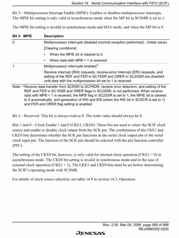
Section 14 Serial Communication Interface with FIFO (SCIF)
Rev. 2.00 Mar 09, 2006 page 569 of 906REJ09B0292-0200
Bit 3�Multiprocessor Interrupt Enable (MPIE): Enables or disables multiprocessor interrupts.The MPIE bit setting is only valid in asynchronous mode when the MP bit in SCSMR is set to 1.
The MPIE bit setting is invalid in synchronous mode and IrDA mode, and when the MP bit is 0.
Bit 3: MPIE Description
0 Multiprocessor interrupts disabled (normal reception performed) (Initial value)
[Clearing conditions]
• When the MPIE bit is cleared to 0
• When data with MPB = 1 is received1 Multiprocessor interrupts enabled*
Receive interrupt (RXI) requests, receive-error interrupt (ERI) requests, andsetting of the RDF and FER in SC1SSR and ORER in SC2SSR are disableduntil data with the multiprocessor bit set to 1 is received.
Note: * Receive data transfer from SCRSR to SCFRDR, receive error detection, and setting of theRDF and FER in SC1SSR and ORER flags in SC2SSR, is not performed. When receivedata with MPB = 1 is received, the MPB flag in SC2SSR is set to 1, the MPIE bit is clearedto 0 automatically, and generation of RXI and ERI (when the RIE bit in SCSCR is set to 1)and FER and ORER flag setting is enabled.
Bit 2�Reserved: This bit is always read as 0. The write value should always be 0.
Bits 1 and 0�Clock Enable 1 and 0 (CKE1, CKE0): These bits are used to select the SCIF clocksource and enable or disable clock output from the SCK pin. The combination of the CKE1 andCKE0 bits determines whether the SCK pin functions as the serial clock output pin or the serialclock input pin. The function of the SCK pin should be selected with the pin function controller(PFC).
The setting of the CKE0 bit, however, is only valid for internal clock operation (CKE1 = 0) inasynchronous mode. The CKE0 bit setting is invalid in synchronous mode and in the case ofexternal clock operation (CKE1 = 1). The CKE1 and CKE0 bits must be set before determiningthe SCIF�s operating mode with SCSMR.
For details of clock source selection, see table 14.9 in section 14.3, Operation.

Section 14 Serial Communication Interface with FIFO (SCIF)
Rev. 2.00 Mar 09, 2006 page 570 of 906REJ09B0292-0200
Bit 1:CKE1
Bit 0:CKE0 Description
0 0 Asynchronous mode Internal clock/SCK pin functions as input pin (inputsignal ignored)*1
Synchronous mode Internal clock/SCK pin functions as serial clockoutput*1
1 Asynchronous mode Internal clock/SCK pin functions as clock output*2
Synchronous mode Internal clock/SCK pin functions as serial clockoutput
1 *4 Asynchronous mode External clock/SCK pin functions as clock input*3
Synchronous mode External clock/SCK pin functions as serial clockinput
Notes: 1. Initial value2. Outputs a clock with a frequency of 16/8/4 times the bit rate.3. Inputs a clock with a frequency of 16/8/4 times the bit rate.4. Don�t care
14.2.7 Serial Status 1 Register (SC1SSR)
Bit: 15 14 13 12 11 10 9 8
PER3 PER2 PER1 PER0 FER3 FER2 FER1 FER0
Initial value: 0 0 0 0 0 0 0 0
R/W: R R R R R R R R
Bit: 7 6 5 4 3 2 1 0
ER TEND TDFE BRK FER PER RDF DR
Initial value: 0 1 1 0 0 0 0 0
R/W: R/(W)* R R/(W)* R/(W)* R R R/(W)* R/(W)*
Note: * Only 0 can be written, to clear the flag.
The serial status 1 register (SC1SSR) is a 16-bit register in which the lower 8 bits consist of statusflags that indicate the operating status of the SCIF, and the upper 8 bits indicate the number ofreceive errors in the data in the receive FIFO register.
SC1SSR can be read or written to at all times. However, 1 cannot be written to the ER, TDFE,BRK, RDF, and DR status flags. Also note that in order to clear these flags to 0, they must first beread as 1. The TEND, FER, and PER flags are read-only and cannot be modified.
Section 14 Serial Communication Interface with FIFO (SCIF)
Rev. 2.00 Mar 09, 2006 page 571 of 906REJ09B0292-0200
SC1SSR is initialized to H'0084 by a reset, by the module standby function, and in standby mode.
Bits 15 to 12�Parity Error Count 3 to 0 (PER3 to PER0): These bits indicate the number of databytes in which a parity error occurred in the receive data in the receive FIFO data register.
These bits are cleared by reading all the receive data in the receive FIFO data register, or bysetting the RFRST bit to 1 in SCFCR and resetting the receive FIFO data register to the emptystate.
Bits 11 to 8�Framing Error Count 3 to 0 (FER3 to FER0): These bits indicate the number of databytes in which a framing error occurred in the receive data in the receive FIFO data register.
These bits are cleared by reading all the receive data in the receive FIFO data register, or bysetting the RFRST bit to 1 in SCFCR and resetting the receive FIFO data register to the emptystate.
Bit 7�Receive Error (ER)
Bit 7: ER Description
0 Reception in progress, or reception has ended normally*1 (Initial value)
[Clearing conditions]
• In a reset or in standby mode
• When 0 is written to ER after reading ER = 11 A framing error, parity error, or overrun error occurred during reception
[Setting conditions]
• When the SCIF checks whether the stop bit at the end of the receive data is1 when reception ends, and the stop bit is 0*2
• When, in reception, the number of 1-bits in the receive data plus the paritybit does not match the parity setting (even or odd) specified by the O/E bitin the serial mode register (SCSMR)
• When the next serial receive operation is completed while there are 16receive data bytes in SCFRDR
Notes: 1. The ER flag is not affected and retains its previous state when the RE bit in SCSCR iscleared to 0. When a framing error or parity error occurs, the receive data is stilltransferred to SCFRDR, and reception is then halted or continued according to thesetting of the EI bit. When an overrun error occurs, the receive data is not transferred toSCFRDR and reception cannot be continued.
2. In 2-stop-bit mode, only the first stop bit is checked for a value of 1; the second stop bitis not checked.
Section 14 Serial Communication Interface with FIFO (SCIF)
Rev. 2.00 Mar 09, 2006 page 572 of 906REJ09B0292-0200
Bit 6�Transmit End (TEND): Indicates that there is no valid data in SCFTDR when the last bit ofthe transmit character is sent, and transmission has been ended.
Bit 6: TEND Description
0 Transmission is in progress
[Clearing condition]
When data is written to SCFTDR while TE = 1
1 Transmission has been ended (Initial value)
[Setting conditions]
• In a reset or in standby mode
• When the TE bit in SCSCR is 0
• When there is no transmit data in SCFTDR on transmission of the last bit ofa 1-byte serial transmit character
Bit 5�Transmit Data FIFO Empty (TDFE): Indicates that data has been transferred from thetransmit FIFO data register (SCFTDR) to the transmit shift register (SCTSR), the number of databytes in SCFTDR has fallen to or below the transmit trigger data number set by bits TTRG1 andTTRG0 in the FIFO control register (SCFCR), and transmit data can be written to SCFTDR.
Bit 5: TDFE Description
0 A number of transmit data bytes exceeding the transmit trigger set numberhave been written to SCFTDR
[Clearing conditions]
• When transmit data exceeding the transmit trigger set number is written toSCFTDR, and 0 is written to TDFE after reading TDFE = 1
• When transmit data exceeding the transmit trigger set number is written toSCFTDR by the on-chip DMAC
1 The number of transmit data bytes in SCFTDR does not exceed the transmittrigger set number (Initial value)
[Setting conditions]
• In a reset or in standby mode
• When the number of SCFTDR transmit data bytes falls to or below thetransmit trigger set number as the result of a transmit operation*
Note: * As SCFTDR is a 16-byte FIFO register, the maximum number of bytes that can be writtenwhen TDFE = 0 is {16 � (transmit trigger set number)}. Data written in excess of this will beignored. The number of data bytes in SCFTDR is indicated by the upper 8 bits of SCFDR.
Section 14 Serial Communication Interface with FIFO (SCIF)
Rev. 2.00 Mar 09, 2006 page 573 of 906REJ09B0292-0200
Bit 4�Break Detect (BRK): Indicates that a receive data break signal has been detected.
Bit 4: BRK Description
0 A break signal has not been received (Initial value)
[Clearing conditions]
• In a reset or in standby mode
• When 0 is written to BRK after reading BRK = 11 A break signal has been received
[Setting condition]
When data with a framing error is received, and a framing error also occurs inthe next receive data (all space �0�)
Note: When a break is detected, transfer to SCFRDR of the receive data (H'00) followingdetection is halted. When the break ends and the receive signal returns to mark �1�, receivedata transfer is resumed.
Bit 3�Framing Error (FER): Indicates a framing error in the data read from the receive FIFO dataregister (SCFRDR).
Bit 3: FER Description
0 There is no framing error in the receive data read from SCFRDR (Initial value)
[Clearing conditions]
• In a reset or in standby mode
• When there is no framing error in SCFRDR read data1 There is a framing error in the receive data read from SCFRDR
[Setting condition]
When there is a framing error in SCFRDR read data
Bit 2�Parity Error (PER): In asynchronous mode, indicates a parity error in the data read fromthe receive FIFO data register (SCFRDR).
Bit 2: PER Description0 There is no parity error in the receive data read from SCFRDR (Initial value)
[Clearing conditions]• In a reset or in standby mode• When there is no parity error in SCFRDR read data
1 There is a parity error in the receive data read from SCFRDR[Setting condition]When there is a parity error in SCFRDR read data
Section 14 Serial Communication Interface with FIFO (SCIF)
Rev. 2.00 Mar 09, 2006 page 574 of 906REJ09B0292-0200
Bit 1�Receive Data Register Full (RDF): Indicates that the received data has been transferred tothe receive FIFO data register (SCFRDR), and the number of receive data bytes in SCFRDR isequal to or greater than the receive trigger number set by bits RTRG1 and RTRG0 in the FIFOcontrol register (SCFCR).
Bit 1: RDF Description
0 The number of receive data bytes in SCFRDR is less than the receive triggerset number (Initial value)
[Clearing conditions]
• In a reset or in standby mode
• When SCFRDR is read until the number of receive data bytes in SCFRDRfalls below the receive trigger set number, and 0 is written to RDF afterreading RDF = 1
• When SCFRDR is read by the on-chip DMAC until the number of receivedata bytes in SCFRDR falls below the receive trigger set number
1 The number of receive data bytes in SCFRDR is equal to or greater than thereceive trigger set number
[Setting condition]
When SCFRDR contains at least the receive trigger set number of receive databytes
Note: SCFRDR is a 16-byte FIFO register. When RDF = 1, at least the receive trigger set numberof data bytes can be read. If all the data in SCFRDR is read and another read is performed,the data value will be undefined. The number of receive data bytes in SCFRDR is indicatedby the lower 8 bits of SCFDR.

Section 14 Serial Communication Interface with FIFO (SCIF)
Rev. 2.00 Mar 09, 2006 page 575 of 906REJ09B0292-0200
Bit 0�Receive Data Ready (DR): Indicates that there are fewer than the receive trigger setnumber of data bytes in the receive FIFO data register (SCFRDR), and no further data has arrivedfor at least 16 etu after the stop bit of the last data received.
Bit 0: DR Description
0 Reception is in progress or has ended normally and there is no receive data leftin SCFRDR (Initial value)
[Clearing conditions]
• In a reset or in standby mode
• When 0 is written to DR after all the remaining receive data has beenread*1
1 No further receive data has arrived, and SCFRDR contains fewer than thereceive trigger set number of data bytes
[Setting condition]
When SCFRDR contains fewer than the receive trigger set number of receivedata bytes, and no further data has arrived for at least 16 etu after the stop bitof the last data received*2
Notes: 1. All remaining receive data should be read before clearing the DR flag.2. Equivalent to 1.6 frames when using an 8-bit, 1-stop-bit format.
etu: Elementary time unit = sec/bit
14.2.8 Serial Status 2 Register (SC2SSR)
Bit: 7 6 5 4 3 2 1 0
TLM RLM N1 N0 MPB MPBT EI ORER
Initial value: 0 0 1 0 0 0 0 0
R/W: R/W R/W R/W R/W R R/W R/W R/(W)*
Note: * Only 0 can be written, to clear the flag.
The serial status 2 register (SC2SSR) is an 8-bit register.
SC2SSR can be read or written to at all times. However, 1 cannot be written to the ORER flag.Also note that in order to clear this flag to 0, they must first be read as 1.
SC2SSR is initialized to H'20 by a reset, by the module standby function, and in standby mode.
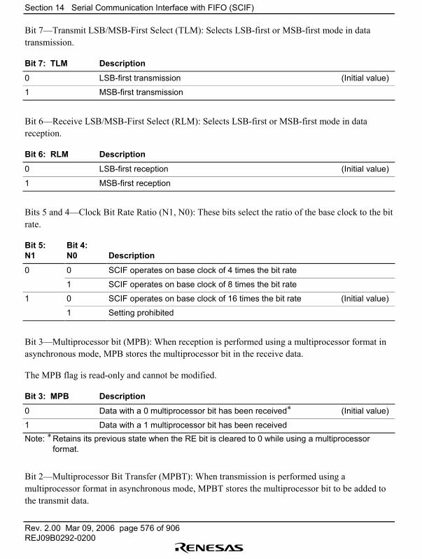
Section 14 Serial Communication Interface with FIFO (SCIF)
Rev. 2.00 Mar 09, 2006 page 576 of 906REJ09B0292-0200
Bit 7�Transmit LSB/MSB-First Select (TLM): Selects LSB-first or MSB-first mode in datatransmission.
Bit 7: TLM Description
0 LSB-first transmission (Initial value)
1 MSB-first transmission
Bit 6�Receive LSB/MSB-First Select (RLM): Selects LSB-first or MSB-first mode in datareception.
Bit 6: RLM Description
0 LSB-first reception (Initial value)
1 MSB-first reception
Bits 5 and 4�Clock Bit Rate Ratio (N1, N0): These bits select the ratio of the base clock to the bitrate.
Bit 5:N1
Bit 4:N0 Description
0 0 SCIF operates on base clock of 4 times the bit rate
1 SCIF operates on base clock of 8 times the bit rate
1 0 SCIF operates on base clock of 16 times the bit rate (Initial value)
1 Setting prohibited
Bit 3�Multiprocessor bit (MPB): When reception is performed using a multiprocessor format inasynchronous mode, MPB stores the multiprocessor bit in the receive data.
The MPB flag is read-only and cannot be modified.
Bit 3: MPB Description
0 Data with a 0 multiprocessor bit has been received* (Initial value)
1 Data with a 1 multiprocessor bit has been receivedNote: * Retains its previous state when the RE bit is cleared to 0 while using a multiprocessor
format.
Bit 2�Multiprocessor Bit Transfer (MPBT): When transmission is performed using amultiprocessor format in asynchronous mode, MPBT stores the multiprocessor bit to be added tothe transmit data.
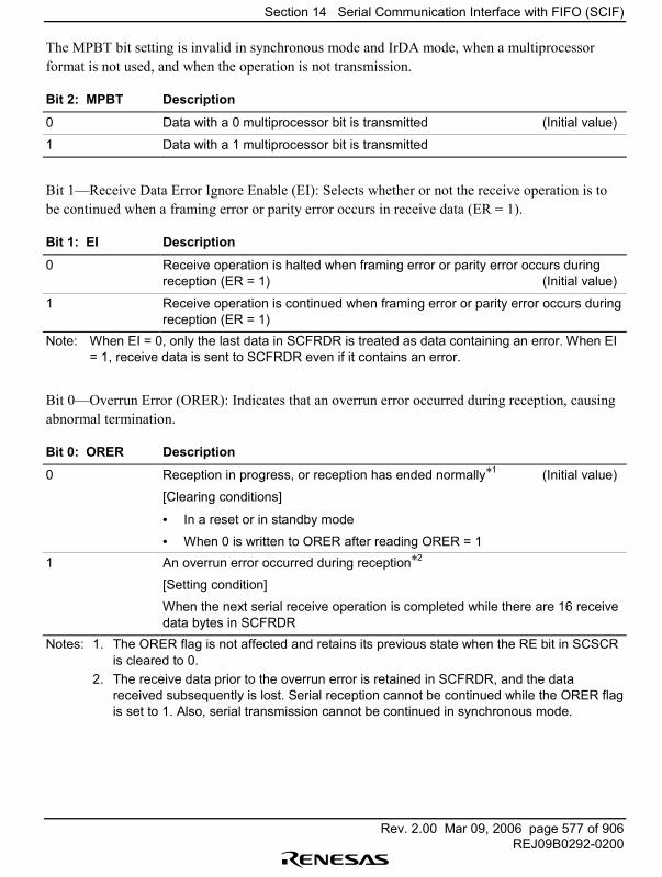
Section 14 Serial Communication Interface with FIFO (SCIF)
Rev. 2.00 Mar 09, 2006 page 577 of 906REJ09B0292-0200
The MPBT bit setting is invalid in synchronous mode and IrDA mode, when a multiprocessorformat is not used, and when the operation is not transmission.
Bit 2: MPBT Description
0 Data with a 0 multiprocessor bit is transmitted (Initial value)
1 Data with a 1 multiprocessor bit is transmitted
Bit 1�Receive Data Error Ignore Enable (EI): Selects whether or not the receive operation is tobe continued when a framing error or parity error occurs in receive data (ER = 1).
Bit 1: EI Description
0 Receive operation is halted when framing error or parity error occurs duringreception (ER = 1) (Initial value)
1 Receive operation is continued when framing error or parity error occurs duringreception (ER = 1)
Note: When EI = 0, only the last data in SCFRDR is treated as data containing an error. When EI= 1, receive data is sent to SCFRDR even if it contains an error.
Bit 0�Overrun Error (ORER): Indicates that an overrun error occurred during reception, causingabnormal termination.
Bit 0: ORER Description
0 Reception in progress, or reception has ended normally*1 (Initial value)
[Clearing conditions]
• In a reset or in standby mode
• When 0 is written to ORER after reading ORER = 11 An overrun error occurred during reception*2
[Setting condition]
When the next serial receive operation is completed while there are 16 receivedata bytes in SCFRDR
Notes: 1. The ORER flag is not affected and retains its previous state when the RE bit in SCSCRis cleared to 0.
2. The receive data prior to the overrun error is retained in SCFRDR, and the datareceived subsequently is lost. Serial reception cannot be continued while the ORER flagis set to 1. Also, serial transmission cannot be continued in synchronous mode.
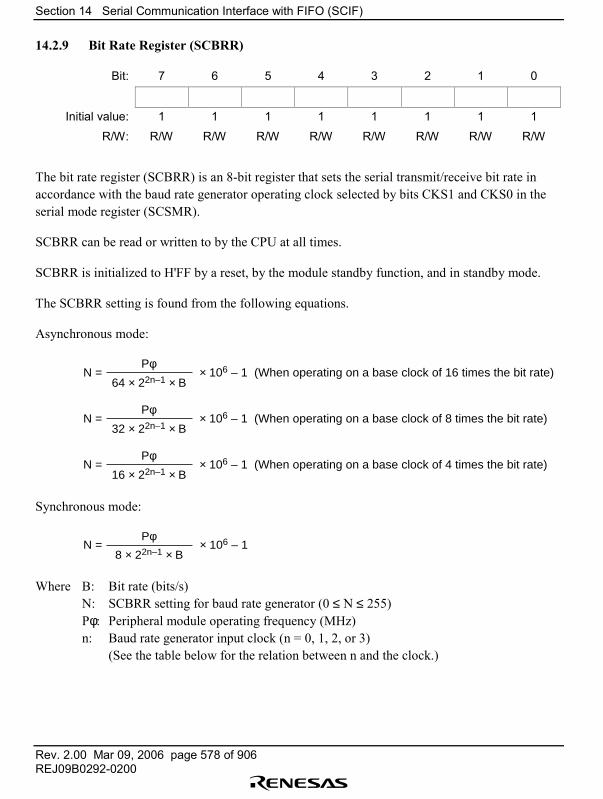
Section 14 Serial Communication Interface with FIFO (SCIF)
Rev. 2.00 Mar 09, 2006 page 578 of 906REJ09B0292-0200
14.2.9 Bit Rate Register (SCBRR)
Bit: 7 6 5 4 3 2 1 0
Initial value: 1 1 1 1 1 1 1 1
R/W: R/W R/W R/W R/W R/W R/W R/W R/W
The bit rate register (SCBRR) is an 8-bit register that sets the serial transmit/receive bit rate inaccordance with the baud rate generator operating clock selected by bits CKS1 and CKS0 in theserial mode register (SCSMR).
SCBRR can be read or written to by the CPU at all times.
SCBRR is initialized to H'FF by a reset, by the module standby function, and in standby mode.
The SCBRR setting is found from the following equations.
Asynchronous mode:
N =64 × 22n–1 × B
× 106 – 1 (When operating on a base clock of 16 times the bit rate)Pφ
N =32 × 22n–1 × B
× 106 – 1 (When operating on a base clock of 8 times the bit rate)Pφ
N =16 × 22n–1 × B
× 106 – 1 (When operating on a base clock of 4 times the bit rate)Pφ
Synchronous mode:
N =8 × 22n–1 × B
× 106 – 1Pφ
Where B: Bit rate (bits/s)N: SCBRR setting for baud rate generator (0 ≤ N ≤ 255)Pφ: Peripheral module operating frequency (MHz)n: Baud rate generator input clock (n = 0, 1, 2, or 3)
(See the table below for the relation between n and the clock.)
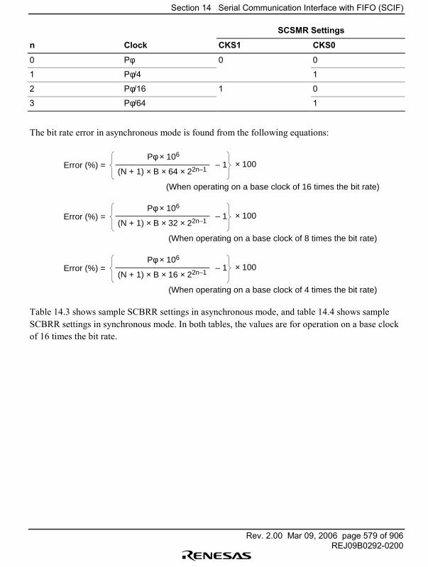
Section 14 Serial Communication Interface with FIFO (SCIF)
Rev. 2.00 Mar 09, 2006 page 579 of 906REJ09B0292-0200
SCSMR Settings
n Clock CKS1 CKS0
0 Pφ 0 0 1 Pφ/4 1 2 Pφ/16 1 0 3 Pφ/64 1
The bit rate error in asynchronous mode is found from the following equations:
Error (%) =(N + 1) × B × 64 × 22n–1 – 1 × 100
Pφ × 106
(When operating on a base clock of 16 times the bit rate)
Error (%) =(N + 1) × B × 32 × 22n–1 – 1 × 100
Pφ × 106
(When operating on a base clock of 8 times the bit rate)
Error (%) =(N + 1) × B × 16 × 22n–1 – 1 × 100
Pφ × 106
(When operating on a base clock of 4 times the bit rate)
Table 14.3 shows sample SCBRR settings in asynchronous mode, and table 14.4 shows sampleSCBRR settings in synchronous mode. In both tables, the values are for operation on a base clockof 16 times the bit rate.
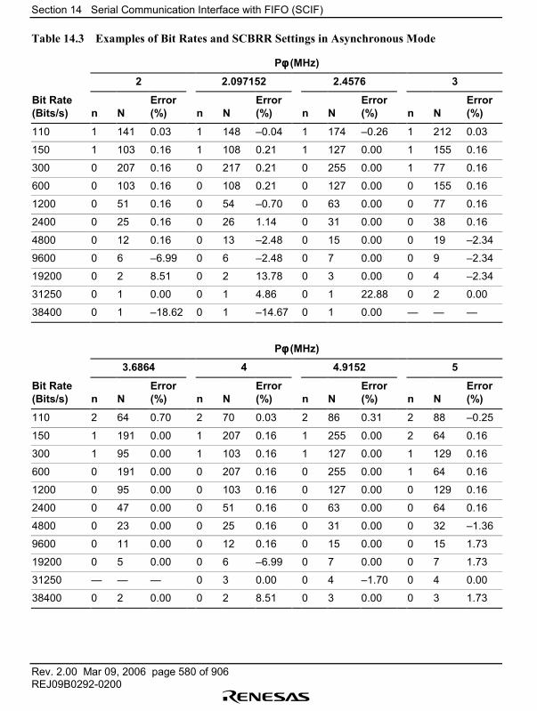
Section 14 Serial Communication Interface with FIFO (SCIF)
Rev. 2.00 Mar 09, 2006 page 580 of 906REJ09B0292-0200
Table 14.3 Examples of Bit Rates and SCBRR Settings in Asynchronous Mode
Pφφφφ (MHz)
2 2.097152 2.4576 3 Bit Rate(Bits/s)
n
N
Error(%)
n
N
Error(%)
n
N
Error(%)
n
N
Error(%)
110 1 141 0.03 1 148 �0.04 1 174 �0.26 1 212 0.03
150 1 103 0.16 1 108 0.21 1 127 0.00 1 155 0.16
300 0 207 0.16 0 217 0.21 0 255 0.00 1 77 0.16
600 0 103 0.16 0 108 0.21 0 127 0.00 0 155 0.16
1200 0 51 0.16 0 54 �0.70 0 63 0.00 0 77 0.16
2400 0 25 0.16 0 26 1.14 0 31 0.00 0 38 0.16
4800 0 12 0.16 0 13 �2.48 0 15 0.00 0 19 �2.34
9600 0 6 �6.99 0 6 �2.48 0 7 0.00 0 9 �2.34
19200 0 2 8.51 0 2 13.78 0 3 0.00 0 4 �2.34
31250 0 1 0.00 0 1 4.86 0 1 22.88 0 2 0.00
38400 0 1 �18.62 0 1 �14.67 0 1 0.00 � � �
Pφφφφ (MHz)
3.6864 4 4.9152 5 Bit Rate(Bits/s)
n
N
Error(%)
n
N
Error(%)
n
N
Error(%)
n
N
Error(%)
110 2 64 0.70 2 70 0.03 2 86 0.31 2 88 �0.25
150 1 191 0.00 1 207 0.16 1 255 0.00 2 64 0.16
300 1 95 0.00 1 103 0.16 1 127 0.00 1 129 0.16
600 0 191 0.00 0 207 0.16 0 255 0.00 1 64 0.16
1200 0 95 0.00 0 103 0.16 0 127 0.00 0 129 0.16
2400 0 47 0.00 0 51 0.16 0 63 0.00 0 64 0.16
4800 0 23 0.00 0 25 0.16 0 31 0.00 0 32 �1.36
9600 0 11 0.00 0 12 0.16 0 15 0.00 0 15 1.73
19200 0 5 0.00 0 6 �6.99 0 7 0.00 0 7 1.73
31250 � � � 0 3 0.00 0 4 �1.70 0 4 0.00
38400 0 2 0.00 0 2 8.51 0 3 0.00 0 3 1.73

Section 14 Serial Communication Interface with FIFO (SCIF)
Rev. 2.00 Mar 09, 2006 page 581 of 906REJ09B0292-0200
Pφφφφ (MHz)
6 6.144 7.37288 8 Bit Rate(Bits/s)
n
N
Error(%)
n
N
Error(%)
n
N
Error(%)
n
N
Error(%)
110 2 106 �0.44 2 108 0.08 2 130 �0.07 2 141 0.03
150 2 77 0.16 2 79 0.00 2 95 0.00 2 103 0.16
300 1 155 0.16 1 159 0.00 1 191 0.00 1 207 0.16
600 1 77 0.16 1 79 0.00 1 95 0.00 1 103 0.16
1200 0 155 0.16 0 159 0.00 0 191 0.00 0 207 0.16
2400 0 77 0.16 0 79 0.00 0 95 0.00 0 103 0.16
4800 0 38 0.16 0 39 0.00 0 47 0.00 0 51 0.16
9600 0 19 �2.34 0 19 0.00 0 23 0.00 0 25 0.16
19200 0 9 �2.34 0 9 0.00 0 11 0.00 0 12 0.16
31250 0 5 0.00 0 5 2.40 0 6 5.33 0 7 0.00
38400 0 4 �2.34 0 4 0.00 0 5 0.00 0 6 �6.99
Pφφφφ (MHz)
9.8304 10 12 12.288
Bit Rate(Bits/s)
n
N
Error(%)
n
N
Error(%)
n
N
Error(%)
n
N
Error(%)
110 2 174 �0.26 2 177 �0.25 2 212 0.03 2 217 0.08
150 2 127 0.00 2 129 0.16 2 155 0.16 2 159 0.00
300 1 255 0.00 2 64 0.16 2 77 0.16 2 79 0.00
600 1 127 0.00 1 129 0.16 1 155 0.16 1 159 0.00
1200 0 255 0.00 1 64 0.16 1 77 0.16 1 79 0.00
2400 0 127 0.00 0 129 0.16 0 155 0.16 0 159 0.00
4800 0 63 0.00 0 64 0.16 0 77 0.16 0 79 0.00
9600 0 31 0.00 0 32 �1.36 0 38 0.16 0 39 0.00
19200 0 15 0.00 0 15 1.73 0 19 �2.34 0 19 0.00
31250 0 9 �1.70 0 9 0.00 0 11 0.00 0 11 2.40
38400 0 7 0.00 0 7 1.73 0 9 �2.34 0 9 0.00

Section 14 Serial Communication Interface with FIFO (SCIF)
Rev. 2.00 Mar 09, 2006 page 582 of 906REJ09B0292-0200
Pφφφφ (MHz)
14.7456 16 30
Bit Rate(Bits/s)
n
N
Error(%)
n
N
Error(%)
n
N
Error(%)
110 3 64 0.70 3 70 0.03 3 132 0.13
150 2 191 0.00 2 207 0.16 3 97 �0.35
300 2 95 0.00 2 103 0.16 2 194 0.16
600 1 191 0.00 1 207 0.16 2 97 �0.35
1200 1 95 0.00 1 103 0.16 1 194 0.16
2400 0 191 0.00 0 207 0.16 1 97 �0.35
4800 0 95 0.00 0 103 0.16 0 194 0.16
9600 0 47 0.00 0 51 0.16 0 97 �0.35
19200 0 23 0.00 0 25 0.16 0 48 �0.35
31250 0 14 �1.70 0 15 0.00 0 29 0.00
38400 0 11 0.00 0 12 0.16 0 23 1.73
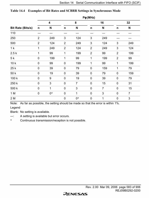
Section 14 Serial Communication Interface with FIFO (SCIF)
Rev. 2.00 Mar 09, 2006 page 583 of 906REJ09B0292-0200
Table 14.4 Examples of Bit Rates and SCBRR Settings in Synchronous Mode
Pφφφφ (MHz)
4 8 16 32
Bit Rate (Bits/s) n N n N n N n N110 � � � � � � � �
250 2 249 3 124 3 249 � �
500 2 124 2 249 3 124 3 249
1 k 1 249 2 124 2 249 3 124
2.5 k 1 99 1 199 2 99 2 199
5 k 0 199 1 99 1 199 2 99
10 k 0 99 0 199 1 99 1 199
25 k 0 39 0 79 0 159 1 79
50 k 0 19 0 39 0 79 0 159
100 k 0 9 0 19 0 39 0 79
250 k 0 3 0 7 0 15 0 31
500 k 0 1 0 3 0 7 0 15
1 M 0 0* 0 1 0 3 0 7
2 M 0 0* 0 1 0 3Note: As far as possible, the setting should be made so that the error is within 1%.LegendBlank: No setting is available.�: A setting is available but error occurs.* Continuous transmission/reception is not possible.
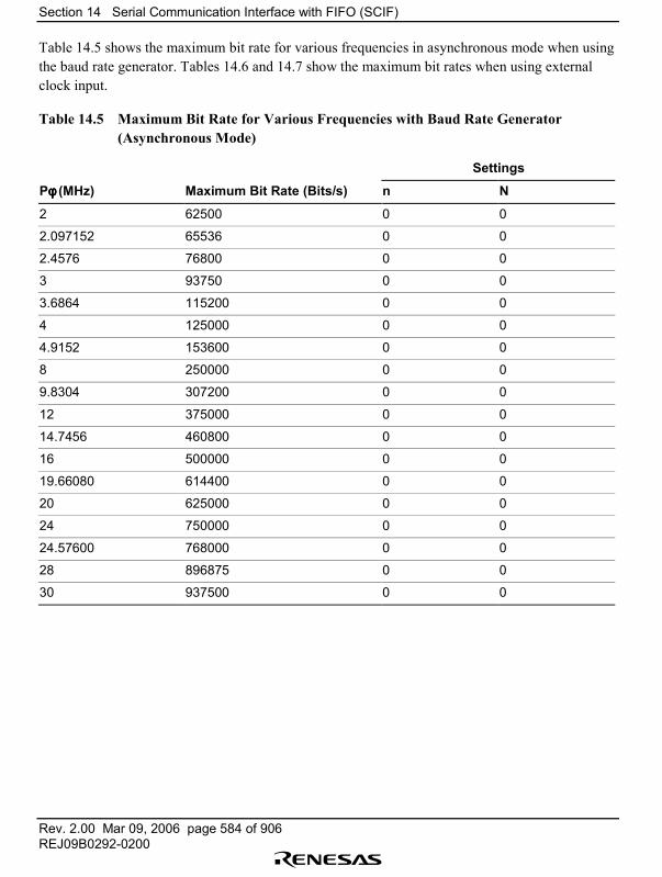
Section 14 Serial Communication Interface with FIFO (SCIF)
Rev. 2.00 Mar 09, 2006 page 584 of 906REJ09B0292-0200
Table 14.5 shows the maximum bit rate for various frequencies in asynchronous mode when usingthe baud rate generator. Tables 14.6 and 14.7 show the maximum bit rates when using externalclock input.
Table 14.5 Maximum Bit Rate for Various Frequencies with Baud Rate Generator(Asynchronous Mode)
Settings
Pφφφφ (MHz) Maximum Bit Rate (Bits/s) n N2 62500 0 0
2.097152 65536 0 0
2.4576 76800 0 0
3 93750 0 0
3.6864 115200 0 0
4 125000 0 0
4.9152 153600 0 0
8 250000 0 0
9.8304 307200 0 0
12 375000 0 0
14.7456 460800 0 0
16 500000 0 0
19.66080 614400 0 0
20 625000 0 0
24 750000 0 0
24.57600 768000 0 0
28 896875 0 0
30 937500 0 0

Section 14 Serial Communication Interface with FIFO (SCIF)
Rev. 2.00 Mar 09, 2006 page 585 of 906REJ09B0292-0200
Table 14.6 Maximum Bit Rate with External Clock Input (Asynchronous Mode)
Pφφφφ (MHz) External Input Clock (MHz) Maximum Bit Rate (Bits/s)
2 0.5000 31250
2.097152 0.5243 32768
2.4576 0.6144 38400
3 0.7500 46875
3.6864 0.9216 57600
4 1.0000 62500
4.9152 1.2288 76800
8 2.0000 125000
9.8304 2.4576 153600
12 3.0000 187500
14.7456 3.6864 230400
16 4.0000 250000
30 7.5000 468750
Table 14.7 Maximum Bit Rate with External Clock Input (Synchronous Mode)
Pφφφφ (MHz) External Input Clock (MHz) Maximum Bit Rate (Bits/s)
8 1.3333 1333333.3
16 2.6667 2666666.7
30 5.0 5000000.0

Section 14 Serial Communication Interface with FIFO (SCIF)
Rev. 2.00 Mar 09, 2006 page 586 of 906REJ09B0292-0200
14.2.10 FIFO Control Register (SCFCR)
Bit: 7 6 5 4 3 2 1 0RTRG1 RTRG0 TTRG1 TTRG0 MCE TFRST RFRST LOOP
Initial value: 0 0 0 0 0 0 0 0R/W: R/W R/W R/W R/W R/W R/W R/W R/W
The FIFO control register (SCFCR) performs data count resetting and trigger data number settingfor the transmit and receive FIFO registers, and also contains a loopback test enable bit.
SCFCR can be read or written to at all times.
SCFCR is initialized to H'00 by a reset, by the module standby function, and in standby mode.
Bits 7 and 6�Receive FIFO Data Number Trigger (RTRG1, RTRG0): These bits are used to setthe number of receive data bytes that sets the receive data full (RDF) flag in the serial status 1register (SC1SSR).
The RDF flag is set when the number of receive data bytes in the receive FIFO data register(SCFRDR) is equal to or greater than the trigger set number shown in the following table.
Bit 7: RTRG1 Bit 6: RTRG0 Receive Trigger Number 0 0 1*
1 4 1 0 8 1 14Note: * Initial value
Bits 5 and 4�Transmit FIFO Data Number Trigger (TTRG1, TTRG0): These bits are used to setthe number of remaining transmit data bytes that sets the transmit FIFO data register empty(TDFE) flag in the serial status 1 register (SC1SSR).
The TDFE flag is set when the number of transmit data bytes in the transmit FIFO data register(SCFTDR) is equal to or less than the trigger set number shown in the following table.
Bit 5: TTRG1 Bit 4: TTRG0 Transmit Trigger Number 0 0 8 (8)*
1 4 (12) 1 0 2 (14) 1 1 (15)Note: * Initial value. Figures in parentheses are the number of empty bytes in SCFTDR when the
flag is set.
Section 14 Serial Communication Interface with FIFO (SCIF)
Rev. 2.00 Mar 09, 2006 page 587 of 906REJ09B0292-0200
Bit 3�Modem Control Enable (MCE): Enables or disables the CTS and RTS modem controlsignals.
Bit 3: MCE Description
0 Modem signals disabled* (Initial value)
1 Modem signals enabledNote: *CTS is fixed at active-0 regardless of the input value, and RTS output is also fixed at 0.
Bit 2�Transmit FIFO Data Register Reset (TFRST): Invalidates the transmit data in the transmitFIFO data register and resets it to the empty state.
Bit 2: TFRST Description
0 Reset operation disabled (Initial value)
1 Reset operation enabledNote: A reset operation is performed in the event of a reset, module standby, or in standby mode.
Bit 1�Receive FIFO Data Register Reset (RFRST): Invalidates the receive data in the receiveFIFO data register and resets it to the empty state.
Bit 1: RFRST Description
0 Reset operation disabled (Initial value)
1 Reset operation enabledNote: A reset operation is performed in the event of a reset, module standby, or in standby mode.
Bit 0�Loopback Test (LOOP): Internally connects the transmit output pin (TxD) and receiveinput pin (RxD), enabling loopback testing.
Bit 0: LOOP Description
0 Loopback test disabled (Initial value)
1 Loopback test enabled
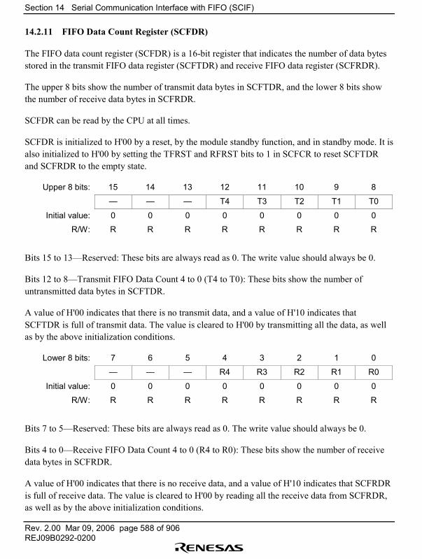
Section 14 Serial Communication Interface with FIFO (SCIF)
Rev. 2.00 Mar 09, 2006 page 588 of 906REJ09B0292-0200
14.2.11 FIFO Data Count Register (SCFDR)
The FIFO data count register (SCFDR) is a 16-bit register that indicates the number of data bytesstored in the transmit FIFO data register (SCFTDR) and receive FIFO data register (SCFRDR).
The upper 8 bits show the number of transmit data bytes in SCFTDR, and the lower 8 bits showthe number of receive data bytes in SCFRDR.
SCFDR can be read by the CPU at all times.
SCFDR is initialized to H'00 by a reset, by the module standby function, and in standby mode. It isalso initialized to H'00 by setting the TFRST and RFRST bits to 1 in SCFCR to reset SCFTDRand SCFRDR to the empty state.
Upper 8 bits: 15 14 13 12 11 10 9 8
� � � T4 T3 T2 T1 T0
Initial value: 0 0 0 0 0 0 0 0R/W: R R R R R R R R
Bits 15 to 13�Reserved: These bits are always read as 0. The write value should always be 0.
Bits 12 to 8�Transmit FIFO Data Count 4 to 0 (T4 to T0): These bits show the number ofuntransmitted data bytes in SCFTDR.
A value of H'00 indicates that there is no transmit data, and a value of H'10 indicates thatSCFTDR is full of transmit data. The value is cleared to H'00 by transmitting all the data, as wellas by the above initialization conditions.
Lower 8 bits: 7 6 5 4 3 2 1 0 � � � R4 R3 R2 R1 R0
Initial value: 0 0 0 0 0 0 0 0R/W: R R R R R R R R
Bits 7 to 5�Reserved: These bits are always read as 0. The write value should always be 0.
Bits 4 to 0�Receive FIFO Data Count 4 to 0 (R4 to R0): These bits show the number of receivedata bytes in SCFRDR.
A value of H'00 indicates that there is no receive data, and a value of H'10 indicates that SCFRDRis full of receive data. The value is cleared to H'00 by reading all the receive data from SCFRDR,as well as by the above initialization conditions.
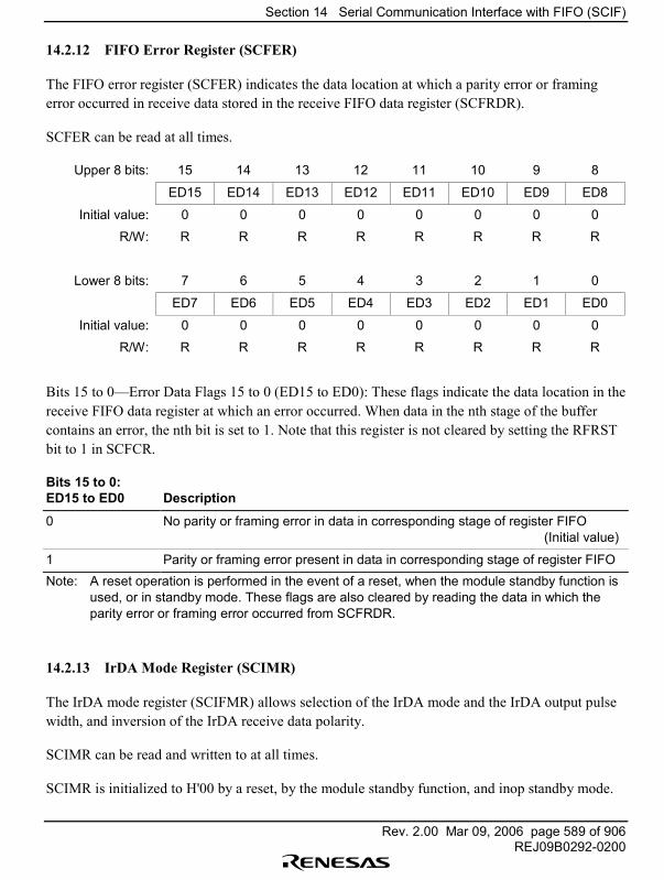
Section 14 Serial Communication Interface with FIFO (SCIF)
Rev. 2.00 Mar 09, 2006 page 589 of 906REJ09B0292-0200
14.2.12 FIFO Error Register (SCFER)
The FIFO error register (SCFER) indicates the data location at which a parity error or framingerror occurred in receive data stored in the receive FIFO data register (SCFRDR).
SCFER can be read at all times.
Upper 8 bits: 15 14 13 12 11 10 9 8 ED15 ED14 ED13 ED12 ED11 ED10 ED9 ED8
Initial value: 0 0 0 0 0 0 0 0R/W: R R R R R R R R
Lower 8 bits: 7 6 5 4 3 2 1 0 ED7 ED6 ED5 ED4 ED3 ED2 ED1 ED0
Initial value: 0 0 0 0 0 0 0 0R/W: R R R R R R R R
Bits 15 to 0�Error Data Flags 15 to 0 (ED15 to ED0): These flags indicate the data location in thereceive FIFO data register at which an error occurred. When data in the nth stage of the buffercontains an error, the nth bit is set to 1. Note that this register is not cleared by setting the RFRSTbit to 1 in SCFCR.
Bits 15 to 0:ED15 to ED0 Description
0 No parity or framing error in data in corresponding stage of register FIFO(Initial value)
1 Parity or framing error present in data in corresponding stage of register FIFONote: A reset operation is performed in the event of a reset, when the module standby function is
used, or in standby mode. These flags are also cleared by reading the data in which theparity error or framing error occurred from SCFRDR.
14.2.13 IrDA Mode Register (SCIMR)
The IrDA mode register (SCIFMR) allows selection of the IrDA mode and the IrDA output pulsewidth, and inversion of the IrDA receive data polarity.
SCIMR can be read and written to at all times.
SCIMR is initialized to H'00 by a reset, by the module standby function, and inop standby mode.
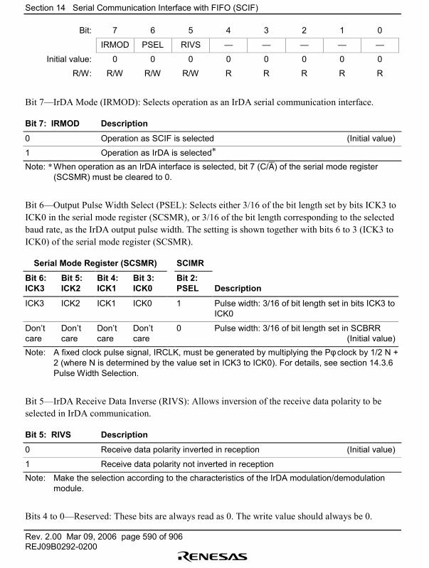
Section 14 Serial Communication Interface with FIFO (SCIF)
Rev. 2.00 Mar 09, 2006 page 590 of 906REJ09B0292-0200
Bit: 7 6 5 4 3 2 1 0
IRMOD PSEL RIVS � � � � �
Initial value: 0 0 0 0 0 0 0 0
R/W: R/W R/W R/W R R R R R
Bit 7�IrDA Mode (IRMOD): Selects operation as an IrDA serial communication interface.
Bit 7: IRMOD Description
0 Operation as SCIF is selected (Initial value)
1 Operation as IrDA is selected*
Note: * When operation as an IrDA interface is selected, bit 7 (C/A) of the serial mode register(SCSMR) must be cleared to 0.
Bit 6�Output Pulse Width Select (PSEL): Selects either 3/16 of the bit length set by bits ICK3 toICK0 in the serial mode register (SCSMR), or 3/16 of the bit length corresponding to the selectedbaud rate, as the IrDA output pulse width. The setting is shown together with bits 6 to 3 (ICK3 toICK0) of the serial mode register (SCSMR).
Serial Mode Register (SCSMR) SCIMR
Bit 6:ICK3
Bit 5:ICK2
Bit 4:ICK1
Bit 3:ICK0
Bit 2:PSEL Description
ICK3 ICK2 ICK1 ICK0 1 Pulse width: 3/16 of bit length set in bits ICK3 toICK0
Don�tcare
Don�tcare
Don�tcare
Don�tcare
0 Pulse width: 3/16 of bit length set in SCBRR(Initial value)
Note: A fixed clock pulse signal, IRCLK, must be generated by multiplying the Pφ clock by 1/2 N +2 (where N is determined by the value set in ICK3 to ICK0). For details, see section 14.3.6Pulse Width Selection.
Bit 5�IrDA Receive Data Inverse (RIVS): Allows inversion of the receive data polarity to beselected in IrDA communication.
Bit 5: RIVS Description
0 Receive data polarity inverted in reception (Initial value)
1 Receive data polarity not inverted in receptionNote: Make the selection according to the characteristics of the IrDA modulation/demodulation
module.
Bits 4 to 0�Reserved: These bits are always read as 0. The write value should always be 0.
Section 14 Serial Communication Interface with FIFO (SCIF)
Rev. 2.00 Mar 09, 2006 page 591 of 906REJ09B0292-0200
14.3 Operation
14.3.1 Overview
The SCIF can carry out serial communication in two modes: asynchronous mode in whichsynchronization is achieved character by character, and synchronous mode in whichsynchronization is achieved with clock pulses.
An IrDA block is also provided, enabling infrared communication conforming to IrDA 1.0 to beexecuted by connecting an infrared transmission/reception unit.
Sixteen-stage FIFO buffers are provided for both transmission and reception, reducing the CPUoverhead and enabling fast, continuous communication to be performed.
Selection of asynchronous, synchronous, or IrDA mode and the transmission format is made bymeans of the serial mode register (SCSMR) and IrDA mode register (SCIMR) as shown in table14.8. The SCIF clock source is determined by a combination of the C/A bit in SCSMR, theIRMOD bit in SCIMR, and the CKE1 and CKE0 bits in the serial control register (SCSCR), asshown in table 14.9.
• Asynchronous Mode Data length: Choice of 7 or 8 bits Choice of parity addition, multiprocessor bit addition, and addition of 1 or 2 stop bits (the
combination of these parameters determines the transmit/receive format and characterlength)
Detection of framing, parity, and overrun errors, receive FIFO data full and receive dataready conditions, and breaks, during reception
Detection of transmit FIFO data empty condition during transmission Choice of internal or external clock as SCIF clock source
When internal clock is selected: The SCIF operates on a clock with a frequency of 16, 8, or4 times the bit rate of the baud rate generator, and can output this operating clock.When external clock is selected: A clock with a frequency of 16, 8, or 4 times the bit ratemust be input (the built-in baud rate generator is not used).
• Synchronous Mode Transmit/receive format: Fixed 8-bit data Detection of overrun errors during reception Choice of internal or external clock as SCIF clock source
When internal clock is selected: The SCIF operates on the baud rate generator clock andcan output a serial clock to external devices.
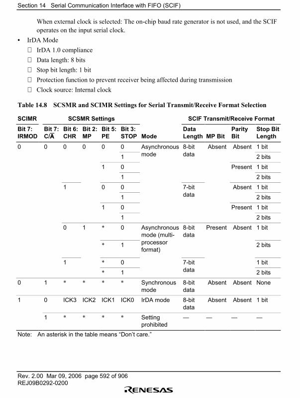
Section 14 Serial Communication Interface with FIFO (SCIF)
Rev. 2.00 Mar 09, 2006 page 592 of 906REJ09B0292-0200
When external clock is selected: The on-chip baud rate generator is not used, and the SCIFoperates on the input serial clock.
• IrDA Mode IrDA 1.0 compliance Data length: 8 bits Stop bit length: 1 bit Protection function to prevent receiver being affected during transmission Clock source: Internal clock
Table 14.8 SCSMR and SCIMR Settings for Serial Transmit/Receive Format Selection
SCIMR SCSMR Settings SCIF Transmit/Receive Format
Bit 7:IRMOD
Bit 7:C/AAAA
Bit 6:CHR
Bit 2:MP
Bit 5:PE
Bit 3:STOP
Mode
DataLength
MP Bit
ParityBit
Stop BitLength
0 0 0 0 0 0 Asynchronous 8-bit Absent Absent 1 bit
1 mode data 2 bits
1 0 Present 1 bit
1 2 bits
1 0 0 7-bit Absent 1 bit
1 data 2 bits
1 0 Present 1 bit
1 2 bits
0 1 * 0 Asynchronousmode (multi-
8-bitdata
Present Absent 1 bit
* 1 processorformat)
2 bits
1 * 0 7-bit 1 bit
* 1 data 2 bits
0 1 * * * * Synchronousmode
8-bitdata
Absent Absent None
1 0 ICK3 ICK2 ICK1 ICK0 IrDA mode 8-bitdata
Absent Absent 1 bit
1 * * * * Settingprohibited
� � � �
Note: An asterisk in the table means �Don�t care.�
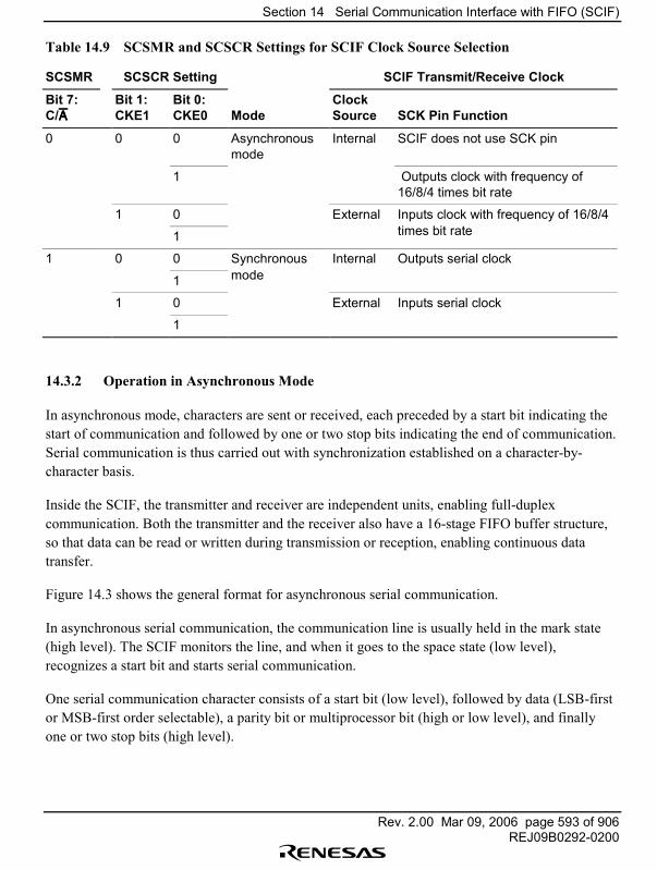
Section 14 Serial Communication Interface with FIFO (SCIF)
Rev. 2.00 Mar 09, 2006 page 593 of 906REJ09B0292-0200
Table 14.9 SCSMR and SCSCR Settings for SCIF Clock Source Selection
SCSMR SCSCR Setting SCIF Transmit/Receive Clock
Bit 7:C/AAAA
Bit 1:CKE1
Bit 0:CKE0
Mode
ClockSource
SCK Pin Function
0 0 0 Asynchronousmode
Internal SCIF does not use SCK pin
1 Outputs clock with frequency of16/8/4 times bit rate
1 0 External Inputs clock with frequency of 16/8/4
1 times bit rate
1 0 0 Synchronous Internal Outputs serial clock
1 mode 1 0 External Inputs serial clock
1
14.3.2 Operation in Asynchronous Mode
In asynchronous mode, characters are sent or received, each preceded by a start bit indicating thestart of communication and followed by one or two stop bits indicating the end of communication.Serial communication is thus carried out with synchronization established on a character-by-character basis.
Inside the SCIF, the transmitter and receiver are independent units, enabling full-duplexcommunication. Both the transmitter and the receiver also have a 16-stage FIFO buffer structure,so that data can be read or written during transmission or reception, enabling continuous datatransfer.
Figure 14.3 shows the general format for asynchronous serial communication.
In asynchronous serial communication, the communication line is usually held in the mark state(high level). The SCIF monitors the line, and when it goes to the space state (low level),recognizes a start bit and starts serial communication.
One serial communication character consists of a start bit (low level), followed by data (LSB-firstor MSB-first order selectable), a parity bit or multiprocessor bit (high or low level), and finallyone or two stop bits (high level).
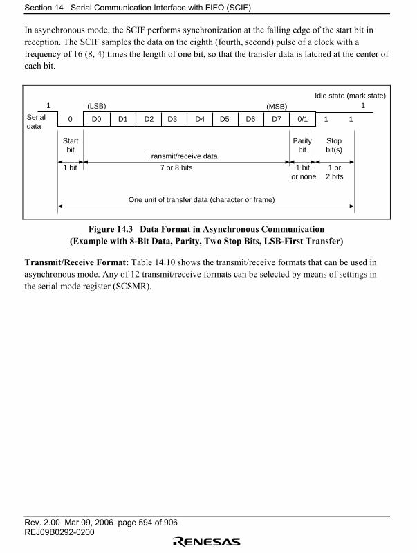
Section 14 Serial Communication Interface with FIFO (SCIF)
Rev. 2.00 Mar 09, 2006 page 594 of 906REJ09B0292-0200
In asynchronous mode, the SCIF performs synchronization at the falling edge of the start bit inreception. The SCIF samples the data on the eighth (fourth, second) pulse of a clock with afrequency of 16 (8, 4) times the length of one bit, so that the transfer data is latched at the center ofeach bit.
Serial data
(LSB)
7 or 8 bits
One unit of transfer data (character or frame)
Paritybit
1 bit,or none
1 or2 bits
1 1
0 D0 D1 D2 D3 D4 D5 D6 D7 0/1 1 1
Idle state (mark state)
Startbit
1 bit
(MSB)
Transmit/receive data
Stopbit(s)
Figure 14.3 Data Format in Asynchronous Communication(Example with 8-Bit Data, Parity, Two Stop Bits, LSB-First Transfer)
Transmit/Receive Format: Table 14.10 shows the transmit/receive formats that can be used inasynchronous mode. Any of 12 transmit/receive formats can be selected by means of settings inthe serial mode register (SCSMR).

Section 14 Serial Communication Interface with FIFO (SCIF)
Rev. 2.00 Mar 09, 2006 page 595 of 906REJ09B0292-0200
Table 14.10 Serial Transmit/Receive Formats (Asynchronous Mode)
SCSMR Settings Serial Transmit/Receive Format and Frame Length CHR PE MP STOP 1 2 3 4 5 6 7 8 9 10 11 12 0 0 0 0 S 8-bit data STOP 1 S 8-bit data STOP STOP 1 0 S 8-bit data P STOP 1 S 8-bit data P STOP STOP 1 0 0 S 8-bit data STOP 1 S 8-bit data STOP STOP 1 0 S 7-bit data P STOP 1 S 7-bit data P STOP STOP 0 * 1 0 S 8-bit data MPB STOP * 1 S 8-bit data MPB STOP STOP 1 * 0 S 7-bit data MPB STOP * 1 S 7-bit data MPB STOP STOP Note: An asterisk in the table means �Don�t care.�LegendS: Start bitSTOP: Stop bitP: Parity bitMPB: Multiprocessor bit
Section 14 Serial Communication Interface with FIFO (SCIF)
Rev. 2.00 Mar 09, 2006 page 596 of 906REJ09B0292-0200
Clock: Either an internal clock generated by the built-in baud rate generator or an external clockinput at the SCK pin can be selected as the SCI�s serial clock, according to the setting of the C/Abit in SCSMR and the CKE1 and CKE0 bits in SCSCR. For details of SCIF clock sourceselection, see table 14.9.
When an external clock is input at the SCK pin, the input clock frequency should be 16, 8, or 4times the bit rate used.
When the SCIF is operated on an internal clock, the clock can be output from the SCK pin. Thefrequency of the clock output in this case is 16, 8, or 4 times the bit rate.
Data Transmit/Receive Operations
• SCIF Initialization (Asynchronous Mode)Before transmitting and receiving data, it is necessary to clear the TE and RE bits to 0 inSCSCR, then initialize the SCIF as described below.When the operating mode, communication format, etc., is changed, the TE and RE bits must becleared to 0 before making the change using the following procedure. When the TE bit iscleared to 0, the transmit shift register (SCTSR) is initialized. Note that clearing the TE and REbits to 0 does not change the contents of the serial status 1 register (SC1SSR), the transmitFIFO data register (SCFTDR), or the receive FIFO data register (SCFRDR). The TE bit shouldnot be cleared to 0 until all transmit data has been transmitted and the TEND flag has been setin SC1SSR. It is possible to clear the TE bit to 0 during transmission, but the data beingtransmitted will go to the high-impedance state after TE is cleared. Also, before startingtransmission by setting TE again, the TFRST bit should first be set to 1 in SCFCR to resetSCFTDR.When an external clock is used the clock should not be stopped during operation, includinginitialization, since operation will be unreliable in this case.Figure 14.4 shows a sample SCIF initialization flowchart.
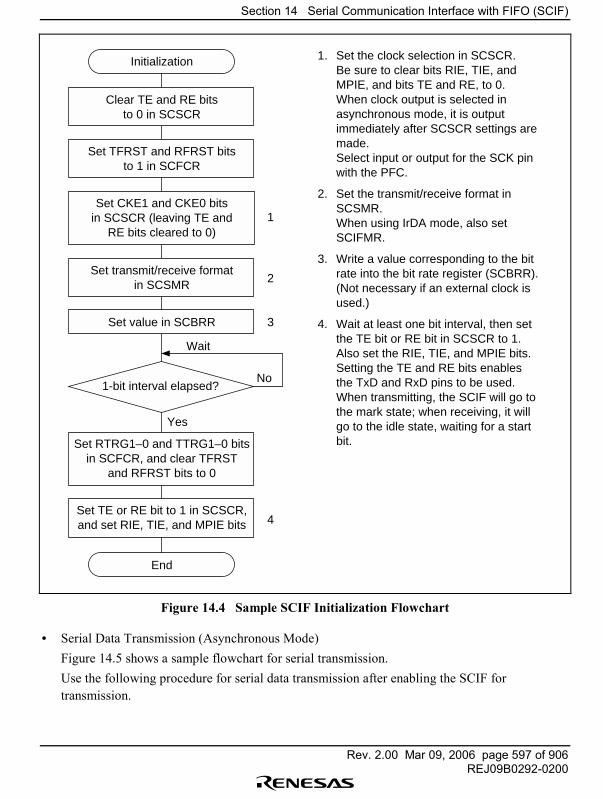
Section 14 Serial Communication Interface with FIFO (SCIF)
Rev. 2.00 Mar 09, 2006 page 597 of 906REJ09B0292-0200
Initialization
Set TFRST and RFRST bitsto 1 in SCFCR
Set CKE1 and CKE0 bitsin SCSCR (leaving TE and
RE bits cleared to 0)
Set transmit/receive formatin SCSMR
Set value in SCBRR
1-bit interval elapsed?
Set RTRG1–0 and TTRG1–0 bitsin SCFCR, and clear TFRST
and RFRST bits to 0
Set TE or RE bit to 1 in SCSCR,and set RIE, TIE, and MPIE bits
End
1
2
3
Clear TE and RE bitsto 0 in SCSCR
4
1. Set the clock selection in SCSCR. Be sure to clear bits RIE, TIE, and
MPIE, and bits TE and RE, to 0. When clock output is selected in
asynchronous mode, it is output immediately after SCSCR settings are made.
Select input or output for the SCK pin with the PFC.
2. Set the transmit/receive format in SCSMR.
When using IrDA mode, also set SCIFMR.
3. Write a value corresponding to the bit rate into the bit rate register (SCBRR). (Not necessary if an external clock is used.)
4. Wait at least one bit interval, then set the TE bit or RE bit in SCSCR to 1. Also set the RIE, TIE, and MPIE bits.
Setting the TE and RE bits enables the TxD and RxD pins to be used. When transmitting, the SCIF will go to the mark state; when receiving, it will go to the idle state, waiting for a start bit.
Yes
No
Wait
Figure 14.4 Sample SCIF Initialization Flowchart
• Serial Data Transmission (Asynchronous Mode)Figure 14.5 shows a sample flowchart for serial transmission.Use the following procedure for serial data transmission after enabling the SCIF fortransmission.
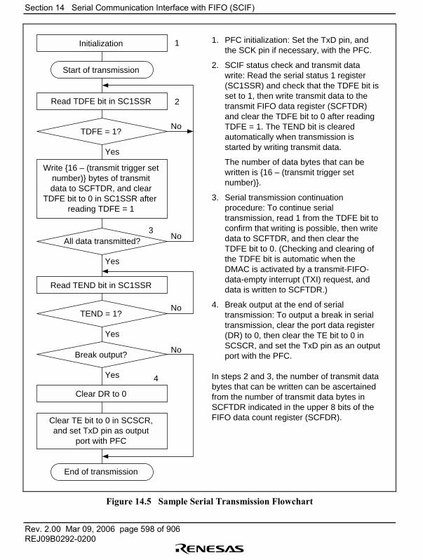
Section 14 Serial Communication Interface with FIFO (SCIF)
Rev. 2.00 Mar 09, 2006 page 598 of 906REJ09B0292-0200
End of transmission
Read TDFE bit in SC1SSR
Write {16 – (transmit trigger setnumber)} bytes of transmitdata to SCFTDR, and clear
TDFE bit to 0 in SC1SSR after reading TDFE = 1
TDFE = 1?
All data transmitted?
Read TEND bit in SC1SSR
TEND = 1?
Break output?
Clear DR to 0
Clear TE bit to 0 in SCSCR,and set TxD pin as output
port with PFC
Start of transmission
Initialization
Yes
No
No
No
No
Yes
Yes
Yes
1
2
3
4
1. PFC initialization: Set the TxD pin, and the SCK pin if necessary, with the PFC.
2. SCIF status check and transmit data write: Read the serial status 1 register (SC1SSR) and check that the TDFE bit is set to 1, then write transmit data to the transmit FIFO data register (SCFTDR) and clear the TDFE bit to 0 after reading TDFE = 1. The TEND bit is cleared automatically when transmission is started by writing transmit data.
The number of data bytes that can be written is {16 – (transmit trigger set number)}.
3. Serial transmission continuation procedure: To continue serial transmission, read 1 from the TDFE bit to confirm that writing is possible, then write data to SCFTDR, and then clear the TDFE bit to 0. (Checking and clearing of the TDFE bit is automatic when the DMAC is activated by a transmit-FIFO-data-empty interrupt (TXI) request, and data is written to SCFTDR.)
4. Break output at the end of serial transmission: To output a break in serial transmission, clear the port data register (DR) to 0, then clear the TE bit to 0 in SCSCR, and set the TxD pin as an output port with the PFC.
In steps 2 and 3, the number of transmit data bytes that can be written can be ascertained from the number of transmit data bytes in SCFTDR indicated in the upper 8 bits of the FIFO data count register (SCFDR).
Figure 14.5 Sample Serial Transmission Flowchart

Section 14 Serial Communication Interface with FIFO (SCIF)
Rev. 2.00 Mar 09, 2006 page 599 of 906REJ09B0292-0200
In serial transmission, the SCIF operates as described below.
1. When data is written to the transmit FIFO data register (SCFTDR), the SCIF transfers the datato the transmit shift register (SCTSR), and starts transmitting. Check that the TDFE flag is setto 1 in the serial status 1 register (SC1SSR) before writing transmit data to SCFTDR. Thenumber of data bytes that can be written is at least {16 � (transmit trigger set number)}.
2. When data is transferred from SCFTDR to SCTSR and transmission is started, transmitoperations are performed continually until there is no transmit data left in SCFTDR. If thenumber of data bytes in SCFTDR falls to or below the transmit trigger number set in the FIFOcontrol register (SCFCR) during transmission, the TDFE flag is set. If the TE bit setting in theserial control register (SCSCR) is 1 at this time, a transmit-FIFO-data-empty interrupt (TXI) isrequested.The serial transmit data is sent from the TxD pin in the following order.
a. Start bit: One 0-bit is output.b. Transmit data: 8-bit or 7-bit data is output in LSB-first or MSB-first order according to the
setting of the TLM bit in SC2SSR.c. Parity bit or multiprocessor bit: One parity bit (even or odd parity), or one multiprocessor
bit is output. (A format in which neither a parity bit nor a multiprocessor bit is output canalso be selected.)
d. Stop bit(s): One or two 1-bits (stop bits) are output.e. Mark state: 1 is output continuously until the start bit that starts the next transmission is
sent.3. The SCIF checks for transmit data in SCFTDR at the timing for sending the stop bit. If there is
data in SCFTDR, it is transferred to SCTSR, the stop bit is sent, and then serial transmission ofthe next frame is started.If there is no transmit data in SCFTDR, the TEND flag is set to 1 in the serial status 1 register(SC1SSR), the stop bit is sent, and then the line goes to the mark state in which 1 is outputcontinuously.Figure 14.6 shows an example of the operation for transmission in asynchronous mode.
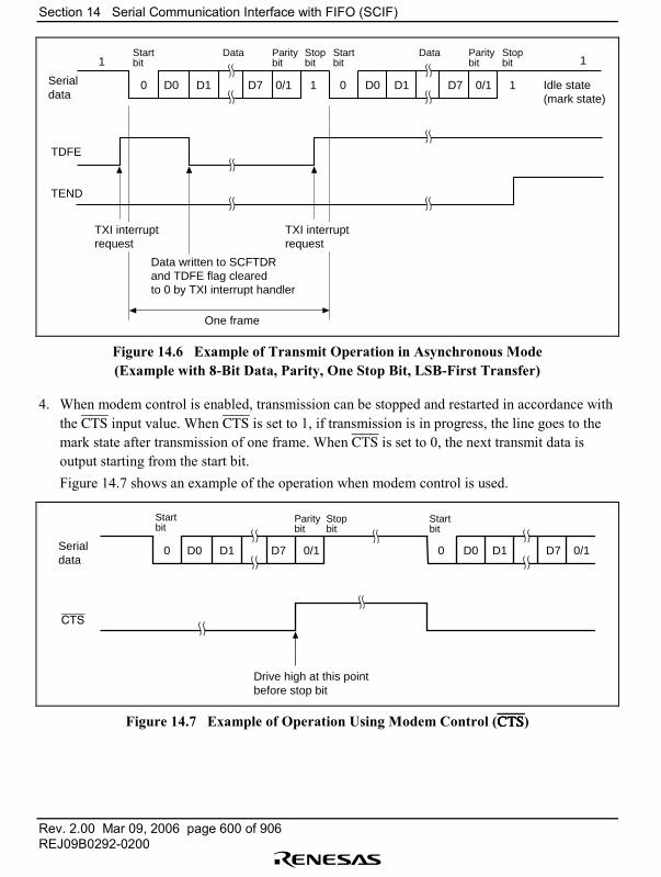
Section 14 Serial Communication Interface with FIFO (SCIF)
Rev. 2.00 Mar 09, 2006 page 600 of 906REJ09B0292-0200
Serial data
1
0 D0 D1 D7 0/1 1 0 D0 D1 D7 0/1 1
1
TDFE
TEND
Startbit
Data Paritybit
Stopbit
Startbit
Idle state(mark state)
Data Paritybit
Stopbit
TXI interrupt request
Data written to SCFTDR and TDFE flag cleared to 0 by TXI interrupt handler
One frame
TXI interrupt request
Figure 14.6 Example of Transmit Operation in Asynchronous Mode(Example with 8-Bit Data, Parity, One Stop Bit, LSB-First Transfer)
4. When modem control is enabled, transmission can be stopped and restarted in accordance withthe CTS input value. When CTS is set to 1, if transmission is in progress, the line goes to themark state after transmission of one frame. When CTS is set to 0, the next transmit data isoutput starting from the start bit.Figure 14.7 shows an example of the operation when modem control is used.
Serial data
0 D0 D1 D7 0/1 0 D0 D1 D7 0/1
CTS
Drive high at this point before stop bit
Startbit
Paritybit
Stopbit
Startbit
Figure 14.7 Example of Operation Using Modem Control (CTSCTSCTSCTS)
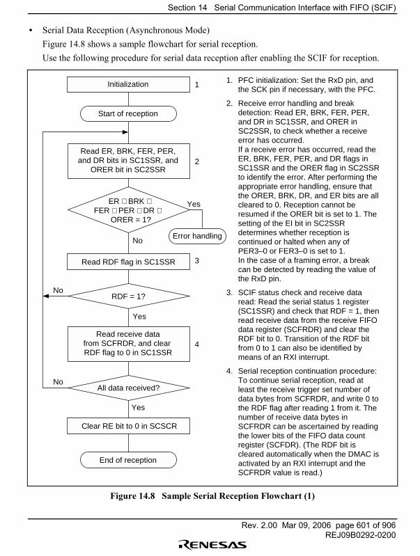
Section 14 Serial Communication Interface with FIFO (SCIF)
Rev. 2.00 Mar 09, 2006 page 601 of 906REJ09B0292-0200
• Serial Data Reception (Asynchronous Mode)Figure 14.8 shows a sample flowchart for serial reception.Use the following procedure for serial data reception after enabling the SCIF for reception.
1. PFC initialization: Set the RxD pin, and the SCK pin if necessary, with the PFC.
2. Receive error handling and break detection: Read ER, BRK, FER, PER, and DR in SC1SSR, and ORER in SC2SSR, to check whether a receive error has occurred.
If a receive error has occurred, read the ER, BRK, FER, PER, and DR flags in SC1SSR and the ORER flag in SC2SSR to identify the error. After performing the appropriate error handling, ensure that the ORER, BRK, DR, and ER bits are all cleared to 0. Reception cannot be resumed if the ORER bit is set to 1. The setting of the EI bit in SC2SSR determines whether reception is continued or halted when any of PER3–0 or FER3–0 is set to 1.
In the case of a framing error, a break can be detected by reading the value of the RxD pin.
3. SCIF status check and receive data read: Read the serial status 1 register
(SC1SSR) and check that RDF = 1, then read receive data from the receive FIFO data register (SCFRDR) and clear the RDF bit to 0. Transition of the RDF bit from 0 to 1 can also be identified by means of an RXI interrupt.
4. Serial reception continuation procedure: To continue serial reception, read at least the receive trigger set number of data bytes from SCFRDR, and write 0 to the RDF flag after reading 1 from it. The number of receive data bytes in SCFRDR can be ascertained by reading the lower bits of the FIFO data count register (SCFDR). (The RDF bit is cleared automatically when the DMAC is activated by an RXI interrupt and the SCFRDR value is read.)
Initialization
Start of reception
Read ER, BRK, FER, PER,and DR bits in SC1SSR, and
ORER bit in SC2SSR
ER ∨ BRK ∨ FER ∨ PER ∨ DR ∨
ORER = 1?
Error handling
Read RDF flag in SC1SSR
RDF = 1?
Read receive datafrom SCFRDR, and clear RDF flag to 0 in SC1SSR
All data received?
Clear RE bit to 0 in SCSCR
End of reception
Yes
No
Yes
No
No
Yes
1
2
3
4
Figure 14.8 Sample Serial Reception Flowchart (1)
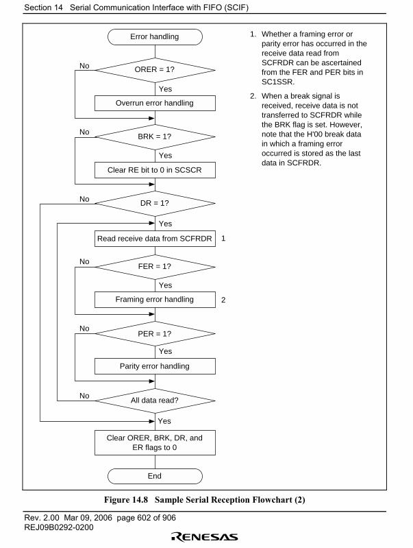
Section 14 Serial Communication Interface with FIFO (SCIF)
Rev. 2.00 Mar 09, 2006 page 602 of 906REJ09B0292-0200
1. Whether a framing error or parity error has occurred in the receive data read from SCFRDR can be ascertained from the FER and PER bits in SC1SSR.
2. When a break signal is received, receive data is not transferred to SCFRDR while the BRK flag is set. However, note that the H'00 break data in which a framing error occurred is stored as the last data in SCFRDR.
Error handling
Overrun error handling
ORER = 1?
BRK = 1?
DR = 1?
FER = 1?
Framing error handling
PER = 1?
Parity error handling
All data read?
Clear ORER, BRK, DR, andER flags to 0
End
No
No
No
No
No
No
Yes
Yes
Yes
Yes
Yes
Yes
Clear RE bit to 0 in SCSCR
Read receive data from SCFRDR 1
2
Figure 14.8 Sample Serial Reception Flowchart (2)
Section 14 Serial Communication Interface with FIFO (SCIF)
Rev. 2.00 Mar 09, 2006 page 603 of 906REJ09B0292-0200
In serial reception, the SCIF operates as described below.
1. The SCIF monitors the communication line, and if a 0 start bit is detected, performs internalsynchronization and starts reception.
2. The received data is stored in SCRSR in LSB-to-MSB order or MSB-to-LSB order accordingto the setting of the RLM bit in SC2SSR.
3. The parity bit and stop bit are received.After receiving these bits, the SCIF carries out the following checks.a. Parity check: The SCIF checks whether the number of 1-bits in the receive data agrees with
the parity (even or odd) set in the O/E bit in the serial mode register (SCSMR).b. Stop bit check: The SCIF checks whether the stop bit is 1. If there are two stop bits, only
the first is checked.c. Status check: The SCIF checks whether receive data can be transferred from the receive
shift register (SCRSR) to SCFRDR.d. Break check: The SCIF checks that the BRK flag is 0, indicating no break.
If all the above checks are passed, the receive data is stored in SCFRDR. If a receive error isdetected in the error check, the operation is as shown in table 14.11.
Note: No further receive operations can be performed when an overrun error has occurred. Thesetting of the EI bit in SC2SSR determines whether reception is continued or halted whena framing error or parity error occurs.
Also, as the RDF flag is not set to 1 when receiving, the error flags must be cleared to 0.
4. If the RIE bit setting in SCSCR is 1 when the RDF or DR flag is set to 1, a receive-FIFO-data-full interrupt (RXI) is requested.If the RIE bit setting in SCSCR is 1 when the ORER, PER, or FER flag is set to 1, a receive-error interrupt (ERI) is requested.If the RIE bit setting in SCSCR is 1 when the BRK flag is set to 1, a break-receive interrupt(BRI) is requested.

Section 14 Serial Communication Interface with FIFO (SCIF)
Rev. 2.00 Mar 09, 2006 page 604 of 906REJ09B0292-0200
Table 14.11 Receive Error Conditions
Receive Error Abbreviation Condition Data Transfer
Overrun error ORER Next serial receive operation iscompleted while there are 16receive data bytes in SCFRDR
Receive data is not transferredfrom SCRSR to SCFRDR
Framing error FER Stop bit is 0 Receive data is transferred fromSCRSR to SCFRDR
Parity error PER Received data parity differsfrom that (even or odd) set inSCSMR
Receive data is transferred fromSCRSR to SCFRDR
Figure 14.9 shows an example of the operation for reception in asynchronous mode.
Serial data
1
0 D0 D1 D7 0/1 1 0 D0 D1 D7 0/1 1
1
RDF
FER
Startbit
Paritybit
Stopbit
Startbit
Data Data Paritybit
Stopbit
Idle state (mark state)
RXI interrupt request
One frame
Data read and RDF flag cleared to 0 by RXI interrupt handler
ERI interrupt request due to framing error
Figure 14.9 Example of SCIF Receive Operation(Example with 8-Bit Data, Parity, One Stop Bit, LSB-First Transfer)
5. When modem control is enabled, the RTS signal is output when SCFRDR is empty. WhenRTS is 0, reception is possible. When RTS is 1, this indicates that SCFRDR is full andreception is not possible.Figure 14.10 shows an example of the operation when modem control is used.
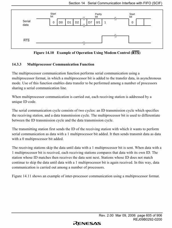
Section 14 Serial Communication Interface with FIFO (SCIF)
Rev. 2.00 Mar 09, 2006 page 605 of 906REJ09B0292-0200
Serial data
0 D0 D1 D2 D7 0/1 01
RTS
Startbit
Paritybit
Startbit
Figure 14.10 Example of Operation Using Modem Control (RTSRTSRTSRTS)
14.3.3 Multiprocessor Communication Function
The multiprocessor communication function performs serial communication using amultiprocessor format, in which a multiprocessor bit is added to the transfer data, in asynchronousmode. Use of this function enables data transfer to be performed among a number of processorssharing a serial communication line.
When multiprocessor communication is carried out, each receiving station is addressed by aunique ID code.
The serial communication cycle consists of two cycles: an ID transmission cycle which specifiesthe receiving station, and a data transmission cycle. The multiprocessor bit is used to differentiatebetween the ID transmission cycle and the data transmission cycle.
The transmitting station first sends the ID of the receiving station with which it wants to performserial communication as data with a 1 multiprocessor bit added. It then sends transmit data as datawith a 0 multiprocessor bit added.
The receiving stations skip the data until data with a 1 multiprocessor bit is sent. When data with a1 multiprocessor bit is received, each receiving stations compares that data with its own ID. Thestation whose ID matches then receives the data sent next. Stations whose ID does not matchcontinue to skip the data until data with a 1 multiprocessor bit is again received. In this way, datacommunication is carried out among a number of processors.
Figure 14.11 shows an example of inter-processor communication using a multiprocessor format.
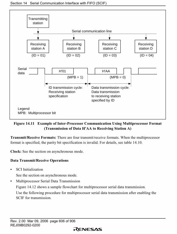
Section 14 Serial Communication Interface with FIFO (SCIF)
Rev. 2.00 Mar 09, 2006 page 606 of 906REJ09B0292-0200
Transmittingstation
Receivingstation A
(ID = 01) (ID = 02) (ID = 03) (ID = 04)
Serial communication line
Serial data
ID transmission cycle: Receiving station specification
Data transmission cycle: Data transmission to receiving station specified by ID
(MPB = 1) (MPB = 0)
H'01 H'AA
LegendMPB: Multiprocessor bit
Receivingstation B
Receivingstation C
Receivingstation D
Figure 14.11 Example of Inter-Processor Communication Using Multiprocessor Format(Transmission of Data H'AA to Receiving Station A)
Transmit/Receive Formats: There are four transmit/receive formats. When the multiprocessorformat is specified, the parity bit specification is invalid. For details, see table 14.10.
Clock: See the section on asynchronous mode.
Data Transmit/Receive Operations
• SCI InitializationSee the section on asynchronous mode.
• Multiprocessor Serial Data TransmissionFigure 14.12 shows a sample flowchart for multiprocessor serial data transmission.Use the following procedure for multiprocessor serial data transmission after enabling theSCIF for transmission.
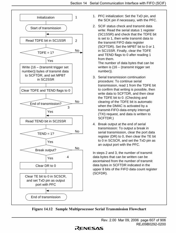
Section 14 Serial Communication Interface with FIFO (SCIF)
Rev. 2.00 Mar 09, 2006 page 607 of 906REJ09B0292-0200
End of transmission
Read TDFE bit in SC1SSR
Write {16 – (transmit trigger set number)} bytes of transmit data
to SCFTDR, and set MPBT in SC2SSR
TDFE = 1?
End of transmission?
Read TEND bit in SC2SSR
TEND = 1?
Break output?
Clear DR to 0
Clear TE bit to 0 in SCSCR,and set TxD pin as output
port with PFC
Start of transmission
Initialization
Yes
No
No
No
No
Yes
Yes
Yes
1
2
3
4
1. PFC initialization: Set the TxD pin, and the SCK pin if necessary, with the PFC.
2. SCIF status check and transmit data write: Read the serial status 1 register (SC1SSR) and check that the TDFE bit is set to 1, then write transmit data to the transmit FIFO data register (SCFTDR). Set the MPBT bit to 0 or 1 in SC1SSR. Finally, clear the TDFE and TEND flags to 0 after reading 1 from them.
The number of data bytes that can be written is {16 – (transmit trigger set number)}.
3. Serial transmission continuation procedure: To continue serial transmission, read 1 from the TDFE bit to confirm that writing is possible, then write data to SCFTDR, and then clear the TDFE bit to 0. (Checking and clearing of the TDFE bit is automatic when the DMAC is activated by a transmit-FIFO-data-empty interrupt (TXI) request, and data is written to SCFTDR.)
4. Break output at the end of serial transmission: To output a break in serial transmission, clear the port data register (DR) to 0, then clear the TE bit to 0 in SCSCR, and set the TxD pin as an output port with the PFC.
In steps 2 and 3, the number of transmit data bytes that can be written can be ascertained from the number of transmit data bytes in SCFTDR indicated in the upper 8 bits of the FIFO data count register (SCFDR).
Clear TDFE and TEND flags to 0
Figure 14.12 Sample Multiprocessor Serial Transmission Flowchart
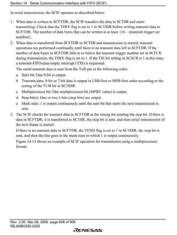
Section 14 Serial Communication Interface with FIFO (SCIF)
Rev. 2.00 Mar 09, 2006 page 608 of 906REJ09B0292-0200
In serial transmission, the SCIF operates as described below.
1. When data is written to SCFTDR, the SCIF transfers the data to SCTSR and startstransmitting. Check that the TDFE flag is set to 1 in SC1SSR before writing transmit data toSCFTDR. The number of data bytes that can be written is at least {16 � (transmit trigger setnumber)}.
2. When data is transferred from SCFTDR to SCTSR and transmission is started, transmitoperations are performed continually until there is no transmit data left in SCFTDR. If thenumber of data bytes in SCFTDR falls to or below the transmit trigger number set in SCFCRduring transmission, the TDFE flag is set to 1. If the TIE bit setting in SCSCR is 1 at this time,a transmit-FIFO-data-empty interrupt (TXI) is requested.The serial transmit data is sent from the TxD pin in the following order.a. Start bit: One 0-bit is output.b. Transmit data: 8-bit or 7-bit data is output in LSB-first or MSB-first order according to the
setting of the TLM bit in SC2SSR.c. Multiprocessor bit: One multiprocessor bit (MPBT value) is output.d. Stop bit(s): One or two 1-bits (stop bits) are output.e. Mark state: 1 is output continuously until the start bit that starts the next transmission is
sent.3. The SCIF checks for transmit data in SCFTDR at the timing for sending the stop bit. If there is
data in SCFTDR, it is transferred to SCTSR, the stop bit is sent, and then serial transmission ofthe next frame is started.If there is no transmit data in SCFTDR, the TEND flag is set to 1 in SC1SSR, the stop bit issent, and then the line goes to the mark state in which 1 is output continuously.Figure 14.13 shows an example of SCIF operation for transmission using a multiprocessorformat.
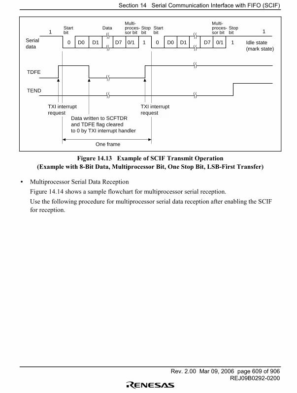
Section 14 Serial Communication Interface with FIFO (SCIF)
Rev. 2.00 Mar 09, 2006 page 609 of 906REJ09B0292-0200
Serial data
1
0 D0 D1 D7 0/1 1 0 D0 D1 D7 0/1 1
1
TDFE
TEND
TXI interrupt request
Startbit
DataMulti-proces-sor bit
Multi-proces-sor bit
Stopbit
Startbit
Stopbit
Idle state(mark state)
Data written to SCFTDR and TDFE flag cleared to 0 by TXI interrupt handler
TXI interrupt request
One frame
Figure 14.13 Example of SCIF Transmit Operation(Example with 8-Bit Data, Multiprocessor Bit, One Stop Bit, LSB-First Transfer)
• Multiprocessor Serial Data ReceptionFigure 14.14 shows a sample flowchart for multiprocessor serial reception.Use the following procedure for multiprocessor serial data reception after enabling the SCIFfor reception.
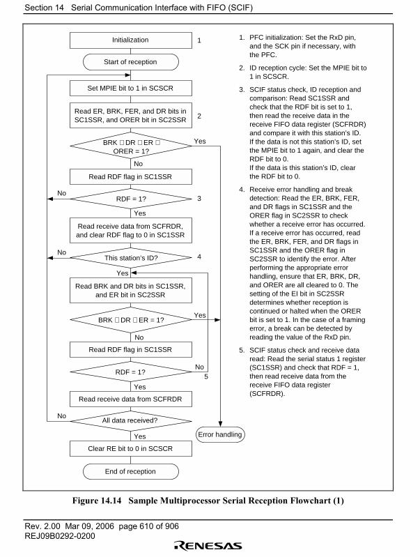
Section 14 Serial Communication Interface with FIFO (SCIF)
Rev. 2.00 Mar 09, 2006 page 610 of 906REJ09B0292-0200
1. PFC initialization: Set the RxD pin, and the SCK pin if necessary, with the PFC.
2. ID reception cycle: Set the MPIE bit to 1 in SCSCR.
3. SCIF status check, ID reception and comparison: Read SC1SSR and check that the RDF bit is set to 1, then read the receive data in the receive FIFO data register (SCFRDR) and compare it with this station’s ID.
If the data is not this station’s ID, set the MPIE bit to 1 again, and clear the RDF bit to 0.
If the data is this station’s ID, clear the RDF bit to 0.
4. Receive error handling and break detection: Read the ER, BRK, FER, and DR flags in SC1SSR and the ORER flag in SC2SSR to check whether a receive error has occurred. If a receive error has occurred, read the ER, BRK, FER, and DR flags in SC1SSR and the ORER flag in SC2SSR to identify the error. After performing the appropriate error handling, ensure that ER, BRK, DR, and ORER are all cleared to 0. The setting of the EI bit in SC2SSR determines whether reception is continued or halted when the ORER bit is set to 1. In the case of a framing error, a break can be detected by reading the value of the RxD pin.
5. SCIF status check and receive data read: Read the serial status 1 register (SC1SSR) and check that RDF = 1, then read receive data from the receive FIFO data register (SCFRDR).
Start of reception
Set MPIE bit to 1 in SCSCR
Read ER, BRK, FER, and DR bits inSC1SSR, and ORER bit in SC2SSR
Initialization
BRK ∨ DR ∨ ER ∨ORER = 1?
Read RDF flag in SC1SSR
RDF = 1?
Read receive data from SCFRDR,and clear RDF flag to 0 in SC1SSR
This station’s ID?
Read BRK and DR bits in SC1SSR,and ER bit in SC2SSR
BRK ∨ DR ∨ ER = 1?
Read RDF flag in SC1SSR
RDF = 1?
Read receive data from SCFRDR
All data received?
Clear RE bit to 0 in SCSCR
End of reception
Error handling
Yes
Yes
No
Yes
Yes
No
No
No
Yes
Yes
No
No
1
2
3
4
5
Figure 14.14 Sample Multiprocessor Serial Reception Flowchart (1)
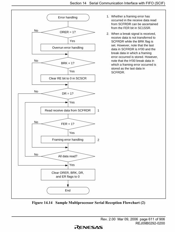
Section 14 Serial Communication Interface with FIFO (SCIF)
Rev. 2.00 Mar 09, 2006 page 611 of 906REJ09B0292-0200
1. Whether a framing error has occurred in the receive data read from SCFRDR can be ascertained from the FER bit in SC1SSR.
2. When a break signal is received, receive data is not transferred to SCFRDR while the BRK flag is set. However, note that the last data in SCFRDR is H'00 and the break data in which a framing error occurred is stored. However, note that the H'00 break data in which a framing error occurred is stored as the last data in SCFRDR.
Error handling
Clear RE bit to 0 in SCSCR
Overrun error handling
Read receive data from SCFRDR
Framing error handling
Clear ORER, BRK, DR,and ER flags to 0
End
ORER = 1?
BRK = 1?
DR = 1?
FER = 1?
All data read?
No
No
No
No
1
2
No
Yes
Yes
Yes
Yes
Yes
Figure 14.14 Sample Multiprocessor Serial Reception Flowchart (2)

Section 14 Serial Communication Interface with FIFO (SCIF)
Rev. 2.00 Mar 09, 2006 page 612 of 906REJ09B0292-0200
Figure 14.15 shows an example of SCIF operation for multiprocessor format reception.
1
0 D0 D1 D7 1 1 0 D0 D1 D7 0 1
1MPB MPB
ID1 ID2 Data2
Serial data
1
0 D0 D1 D7 1 1 0 D0 D1 D7 0 1
1MPB MPB
Idle state (mark state)
MPIE
RDF
SCFRDR value ID1
Startbit Data (ID1)
Stopbit
Startbit
StopbitData (Data1)
Serial data
MPIE
RDF
SCFRDR value
Startbit Data (ID2)
Stopbit
Startbit
StopbitData (Data2)
Idle state (mark state)
RXI interrupt request (multiprocessor interrupt)MPIE = 0
SCFRDR data read and RDF flag cleared to 0 by RXI interrupt handler
As data is not this station’s ID, MPIE bit is set to 1 again
RXI interrupt request is not generated, and SCFRDR retains its state
RXI interrupt request (multiprocessor interrupt)MPIE = 0
SCFRDR data read and RDF flag cleared to 0 by RXI interrupt handler
As data matches this station’s ID, reception continues and data is received by RXI interrupt handler
(a) Data does not match station’s ID
MPIE bit set to 1 again
(b) Data matches station’s ID
Figure 14.15 Example of SCIF Receive Operation(Example with 8-Bit Data, Multiprocessor Bit, One Stop Bit, LSB-First Transfer)
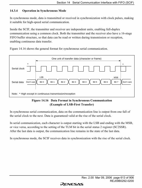
Section 14 Serial Communication Interface with FIFO (SCIF)
Rev. 2.00 Mar 09, 2006 page 613 of 906REJ09B0292-0200
14.3.4 Operation in Synchronous Mode
In synchronous mode, data is transmitted or received in synchronization with clock pulses, makingit suitable for high-speed serial communication.
Inside the SCIF, the transmitter and receiver are independent units, enabling full-duplexcommunication using a common clock. Both the transmitter and the receiver also have a 16-stageFIFO buffer structure, so that data can be read or written during transmission or reception,enabling continuous data transfer.
Figure 14.16 shows the general format for synchronous serial communication.
One unit of transfer data (character or frame)
Serial clock
Serial data
LSB
Bit 0
MSB
* *
Don’t care Don’t care
Note: * High except in continuous transmission/reception
Bit 1 Bit 2 Bit 3 Bit 4 Bit 5 Bit 6 Bit 7
Figure 14.16 Data Format in Synchronous Communication(Example of LSB-First Transfer)
In synchronous serial communication, data on the communication line is output from one fall ofthe serial clock to the next. Data is guaranteed valid at the rise of the serial clock.
In serial communication, each character is output starting with the LSB and ending with the MSB,or vice versa, according to the setting of the TLM bit in the serial status 2 register (SC2SSR).After the last data is output, the communication line remains in the state of the last data.
In synchronous mode, the SCIF receives data in synchronization with the rise of the serial clock.
Section 14 Serial Communication Interface with FIFO (SCIF)
Rev. 2.00 Mar 09, 2006 page 614 of 906REJ09B0292-0200
Transmit/Receive Format: A fixed 8-bit data format is used. No parity or multiprocessor bits areadded.
Clock: Either an internal clock generated by the built-in baud rate generator or an external serialclock input at the SCK pin can be selected, according to the setting of the C/A bit in SCSMR andthe CKE1 and CKE0 bits in SCSCR. For details of SCIF clock source selection, see table 14.9.
When the SCIF is operated on an internal clock, the serial clock is output from the SCK pin.
Eight serial clock pulses are output in the transfer of one character, and when notransmission/reception is performed the clock is fixed high. In receive-only operation, however,the SCIF receives two characters as one unit, and so a 16-pulse serial clock is output. To performsingle-character receive operations, an external clock should be selected as the clock source.
Transmit/Receive Operations
• SCIF Initialization (Synchronous Mode)Before transmitting and receiving data, it is necessary to clear the TE and RE bits to 0 in theserial control register (SCSCR), then initialize the SCIF as described below.When the operating mode, communication format, etc., is changed, the TE and RE bits must becleared to 0 before making the change using the following procedure. When the TE bit iscleared to 0, the TDFE flag is set to 1 and the transmit shift register (SCTSR) is initialized.Note that clearing the RE bit to 0 does not change the contents of the RDF, PER, FER, andORER flags, or the receive FIFO data register (SCFRDR).Figure 14.17 shows a sample SCIF initialization flowchart.
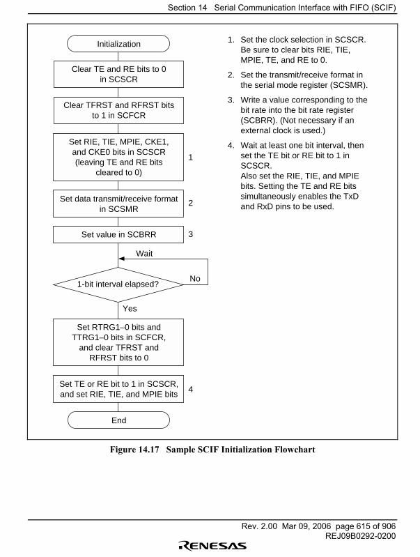
Section 14 Serial Communication Interface with FIFO (SCIF)
Rev. 2.00 Mar 09, 2006 page 615 of 906REJ09B0292-0200
Initialization
Clear TE and RE bits to 0in SCSCR
Clear TFRST and RFRST bitsto 1 in SCFCR
Set RIE, TIE, MPIE, CKE1,and CKE0 bits in SCSCR(leaving TE and RE bits
cleared to 0)
Set data transmit/receive formatin SCSMR
Set RTRG1–0 bits andTTRG1–0 bits in SCFCR,
and clear TFRST andRFRST bits to 0
Set TE or RE bit to 1 in SCSCR,and set RIE, TIE, and MPIE bits
Set value in SCBRR
1-bit interval elapsed?
End
1. Set the clock selection in SCSCR. Be sure to clear bits RIE, TIE, MPIE, TE, and RE to 0.
2. Set the transmit/receive format in the serial mode register (SCSMR).
3. Write a value corresponding to the bit rate into the bit rate register (SCBRR). (Not necessary if an external clock is used.)
4. Wait at least one bit interval, then set the TE bit or RE bit to 1 in SCSCR.
Also set the RIE, TIE, and MPIE bits. Setting the TE and RE bits simultaneously enables the TxD and RxD pins to be used.
Yes
No
Wait
2
3
4
1
Figure 14.17 Sample SCIF Initialization Flowchart
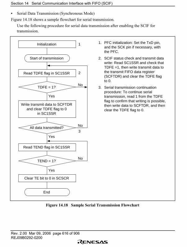
Section 14 Serial Communication Interface with FIFO (SCIF)
Rev. 2.00 Mar 09, 2006 page 616 of 906REJ09B0292-0200
• Serial Data Transmission (Synchronous Mode)Figure 14.18 shows a sample flowchart for serial transmission.
Use the following procedure for serial data transmission after enabling the SCIF fortransmission.
End
Read TDFE flag in SC1SSR
Initialization
Write transmit data to SCFTDRand clear TDFE flag to 0
in SC1SSR
TDFE = 1?
All data transmitted?
Read TEND flag in SC1SSR
TEND = 1?
Clear TE bit to 0 in SCSCR
Start of transmission
Yes
No
No
No
2
1
3Yes
Yes
1. PFC initialization: Set the TxD pin, and the SCK pin if necessary, with the PFC.
2. SCIF status check and transmit data write: Read SC1SSR and check that TDFE =1, then write transmit data to the transmit FIFO data register (SCFTDR) and clear the TDFE flag to 0.
3. Serial transmission continuation procedure: To continue serial transmission, read 1 from the TDFE flag to confirm that writing is possible, then write data to SCFTDR, and then clear the TDFE flag to 0.
Figure 14.18 Sample Serial Transmission Flowchart
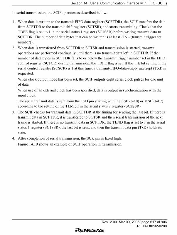
Section 14 Serial Communication Interface with FIFO (SCIF)
Rev. 2.00 Mar 09, 2006 page 617 of 906REJ09B0292-0200
In serial transmission, the SCIF operates as described below.
1. When data is written to the transmit FIFO data register (SCFTDR), the SCIF transfers the datafrom SCFTDR to the transmit shift register (SCTSR), and starts transmitting. Check that theTDFE flag is set to 1 in the serial status 1 register (SC1SSR) before writing transmit data toSCFTDR. The number of data bytes that can be written is at least {16 � (transmit trigger setnumber)}.
2. When data is transferred from SCFTDR to SCTSR and transmission is started, transmitoperations are performed continually until there is no transmit data left in SCFTDR. If thenumber of data bytes in SCFTDR falls to or below the transmit trigger number set in the FIFOcontrol register (SCFCR) during transmission, the TDFE flag is set. If the TIE bit setting in theserial control register (SCSCR) is 1 at this time, a transmit-FIFO-data-empty interrupt (TXI) isrequested.When clock output mode has been set, the SCIF outputs eight serial clock pulses for one unitof data.When use of an external clock has been specified, data is output in synchronization with theinput clock.The serial transmit data is sent from the TxD pin starting with the LSB (bit 0) or MSB (bit 7)according to the setting of the TLM bit in the serial status 2 register (SC2SSR).
3. The SCIF checks for transmit data in SCFTDR at the timing for sending the last bit. If there istransmit data in SCFTDR, it is transferred to SCTSR and then serial transmission of the nextframe is started. If there is no transmit data in SCFTDR, the TEND flag is set to 1 in the serialstatus 1 register (SC1SSR), the last bit is sent, and then the transmit data pin (TxD) holds itsstate.
4. After completion of serial transmission, the SCK pin is fixed high.Figure 14.19 shows an example of SCIF operation in transmission.
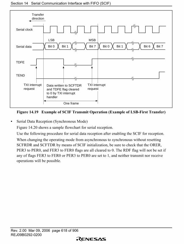
Section 14 Serial Communication Interface with FIFO (SCIF)
Rev. 2.00 Mar 09, 2006 page 618 of 906REJ09B0292-0200
LSB
TDFE
TEND
Bit 0 Bit 1 Bit 7 Bit 0 Bit 1 Bit 6 Bit 7
Transfer direction
Serial clock
Serial data
TXI interrupt request
Data written to SCFTDR and TDFE flag cleared to 0 by TXI interrupt handler
One frame
TXI interrupt request
MSB
Figure 14.19 Example of SCIF Transmit Operation (Example of LSB-First Transfer)
• Serial Data Reception (Synchronous Mode)Figure 14.20 shows a sample flowchart for serial reception.Use the following procedure for serial data reception after enabling the SCIF for reception.When changing the operating mode from asynchronous to synchronous without resettingSCFRDR and SCFTDR by means of SCIF initialization, be sure to check that the ORER,PER3 to PER0, and FER3 to FER0 flags are all cleared to 0. The RDF flag will not be set ifany of flags FER3 to FER0 or PER3 to PER0 are set to 1, and neither transmit nor receiveoperations will be possible.
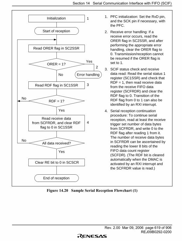
Section 14 Serial Communication Interface with FIFO (SCIF)
Rev. 2.00 Mar 09, 2006 page 619 of 906REJ09B0292-0200
1. PFC initialization: Set the RxD pin, and the SCK pin if necessary, with the PFC.
2. Receive error handling: If a receive error occurs, read the ORER flag in SC2SSR, and after performing the appropriate error handling, clear the ORER flag to 0. Transmission/reception cannot be resumed if the ORER flag is set to 1.
3. SCIF status check and receive data read: Read the serial status 1 register (SC1SSR) and check that RDF = 1, then read receive data from the receive FIFO data register (SCFRDR) and clear the RDF flag to 0. Transition of the RDF flag from 0 to 1 can also be identified by an RXI interrupt.
4. Serial reception continuation procedure: To continue serial reception, read at least the receive trigger set number of data bytes from SCFRDR, and write 0 to the RDF flag after reading 1 from it.
The number of receive data bytes in SCFRDR can be ascertained by reading the lower 8 bits of the FIFO data count register (SCFDR). (The RDF bit is cleared automatically when the DMAC is activated by an RXI interrupt and the SCFRDR value is read.)
Start of reception
Read ORER flag in SC2SSR
Initialization
Error handling
2
3
4
1
Read RDF flag in SC1SSR
RDF = 1?
Read receive datafrom SCFRDR, and clear RDF
flag to 0 in SC1SSR
All data received?
Clear RE bit to 0 in SCSCR
End of reception
Yes
No
Yes
No
No
Yes
ORER = 1?
Figure 14.20 Sample Serial Reception Flowchart (1)
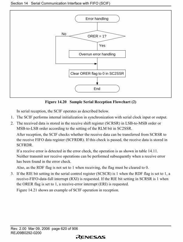
Section 14 Serial Communication Interface with FIFO (SCIF)
Rev. 2.00 Mar 09, 2006 page 620 of 906REJ09B0292-0200
Error handling
Overrun error handling
Yes
NoORER = 1?
Clear ORER flag to 0 in SC2SSR
End
Figure 14.20 Sample Serial Reception Flowchart (2)
In serial reception, the SCIF operates as described below.1. The SCIF performs internal initialization in synchronization with serial clock input or output.2. The received data is stored in the receive shift register (SCRSR) in LSB-to-MSB order or
MSB-to-LSB order according to the setting of the RLM bit in SC2SSR.After reception, the SCIF checks whether the receive data can be transferred from SCRSR tothe receive FIFO data register (SCFRDR). If this check is passed, the receive data is stored inSCFRDR.If a receive error is detected in the error check, the operation is as shown in table 14.11.Neither transmit nor receive operations can be performed subsequently when a receive errorhas been found in the error check.Also, as the RDF flag is not set to 1 when receiving, the flag must be cleared to 0.
3. If the RIE bit setting in the serial control register (SCSCR) is 1 when the RDF flag is set to 1, areceive-FIFO-data-full interrupt (RXI) is requested. If the RIE bit setting in SCRSR is 1 whenthe ORER flag is set to 1, a receive-error interrupt (ERI) is requested.Figure 14.21 shows an example of SCIF operation in reception.
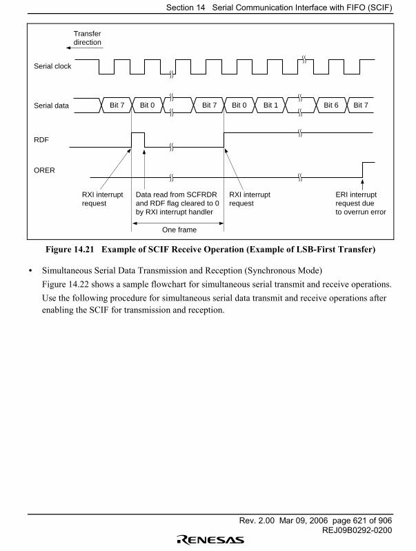
Section 14 Serial Communication Interface with FIFO (SCIF)
Rev. 2.00 Mar 09, 2006 page 621 of 906REJ09B0292-0200
Serial clock
Serial data
Transfer direction
Data read from SCFRDR and RDF flag cleared to 0 by RXI interrupt handler
RXI interrupt request
RDF
ORER
Bit 7 Bit 0 Bit 7 Bit 0 Bit 1 Bit 6 Bit 7
RXI interrupt request
ERI interrupt request due to overrun error
One frame
Figure 14.21 Example of SCIF Receive Operation (Example of LSB-First Transfer)
• Simultaneous Serial Data Transmission and Reception (Synchronous Mode)Figure 14.22 shows a sample flowchart for simultaneous serial transmit and receive operations.Use the following procedure for simultaneous serial data transmit and receive operations afterenabling the SCIF for transmission and reception.
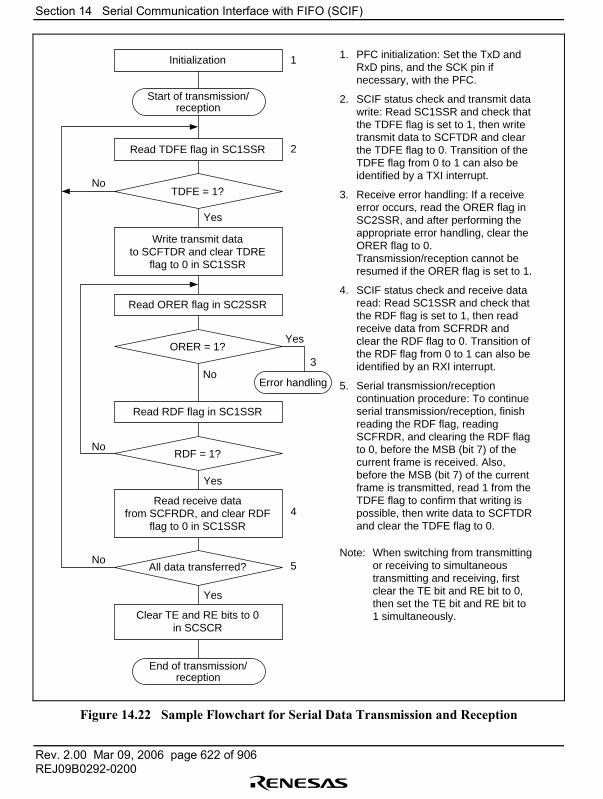
Section 14 Serial Communication Interface with FIFO (SCIF)
Rev. 2.00 Mar 09, 2006 page 622 of 906REJ09B0292-0200
1. PFC initialization: Set the TxD and RxD pins, and the SCK pin if necessary, with the PFC.
2. SCIF status check and transmit data write: Read SC1SSR and check that the TDFE flag is set to 1, then write transmit data to SCFTDR and clear the TDFE flag to 0. Transition of the TDFE flag from 0 to 1 can also be identified by a TXI interrupt.
3. Receive error handling: If a receive error occurs, read the ORER flag in SC2SSR, and after performing the appropriate error handling, clear the ORER flag to 0. Transmission/reception cannot be resumed if the ORER flag is set to 1.
4. SCIF status check and receive data read: Read SC1SSR and check that the RDF flag is set to 1, then read receive data from SCFRDR and clear the RDF flag to 0. Transition of the RDF flag from 0 to 1 can also be identified by an RXI interrupt.
5. Serial transmission/reception continuation procedure: To continue serial transmission/reception, finish reading the RDF flag, reading SCFRDR, and clearing the RDF flag to 0, before the MSB (bit 7) of the current frame is received. Also, before the MSB (bit 7) of the current frame is transmitted, read 1 from the TDFE flag to confirm that writing is possible, then write data to SCFTDR and clear the TDFE flag to 0.
Note: When switching from transmitting or receiving to simultaneous transmitting and receiving, first clear the TE bit and RE bit to 0, then set the TE bit and RE bit to 1 simultaneously.
Read TDFE flag in SC1SSR
Initialization 1
2
4
5
3
Write transmit datato SCFTDR and clear TDRE
flag to 0 in SC1SSR
Read ORER flag in SC2SSR
Read RDF flag in SC1SSR
Read receive datafrom SCFRDR, and clear RDF
flag to 0 in SC1SSR
Clear TE and RE bits to 0in SCSCR
Error handling
Start of transmission/reception
TDFE = 1?
ORER = 1?
RDF = 1?
All data transferred?
End of transmission/reception
Yes
No
Yes
No
No
Yes
Yes
No
Figure 14.22 Sample Flowchart for Serial Data Transmission and Reception
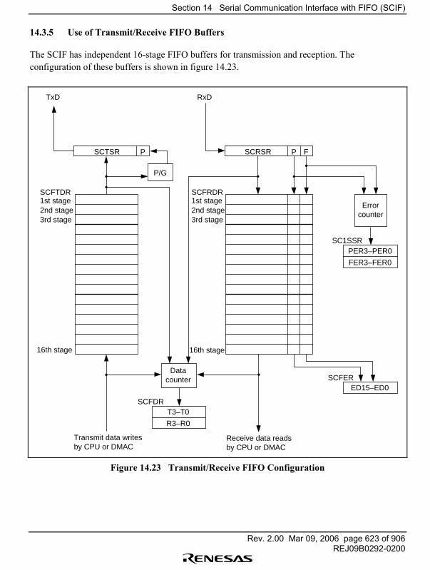
Section 14 Serial Communication Interface with FIFO (SCIF)
Rev. 2.00 Mar 09, 2006 page 623 of 906REJ09B0292-0200
14.3.5 Use of Transmit/Receive FIFO Buffers
The SCIF has independent 16-stage FIFO buffers for transmission and reception. Theconfiguration of these buffers is shown in figure 14.23.
TxD RxD
SCTSR
T3–T0
Transmit data writes by CPU or DMAC
Receive data reads by CPU or DMAC
R3–R0
P
P/G
ED15–ED0
PER3–PER0SC1SSR
FER3–FER0
1st stage2nd stage3rd stage
Datacounter
Errorcounter
16th stage
SCFTDR SCFRDR
SCFDR
SCFER
SCRSR P F
16th stage
1st stage2nd stage3rd stage
Figure 14.23 Transmit/Receive FIFO Configuration
Section 14 Serial Communication Interface with FIFO (SCIF)
Rev. 2.00 Mar 09, 2006 page 624 of 906REJ09B0292-0200
In Serial Data Transmit Operations: In transmission, when transmit data is written to thetransmit FIFO by the CPU or DMAC and the TE bit is set to 1 in the serial control register(SCSCR), the data is first transferred to the transmit shift register (SCTSR) in the order of writingto the transmit FIFO, a parity bit is added by the parity generator (P/G), and then serial data istransmitted from the TxD pin.
Each time data is written into the transmit FIFO, the value in bits T4 to T0 in the FIFO data countregister (SCFDR) is incremented, and each time data is transferred to SCTSR the value in bits T4to T0 is decremented. The current number of data bytes in the transmit FIFO can thus be found byreading bits T4 to T0 in SCFDR.
A value of H'10 in bits T4 to T0 means that data has been written into all 16 stages of the transmitFIFO. If additional data is written to the FIFO in this state, bits T4 to T0 will not be incrementedand the written data will be lost.
When the transmit trigger number is set and transmit data is written to the FIFO by the DMAC,care must be taken not to write data exceeding the number of empty bytes in SCFTDR indicatedby the FIFO control register (SCFCR) (see section 14.2.10).
In Serial Data Receive Operations: In reception, serial data input from the RxD pin is firstcaptured in the receive shift register (SCRSR) in the order specified by the RLM bit in the serialstatus 2 register (SC2SSR). A parity bit check is carried out, and if there is a parity error the P(parity error) flag for that data is set to 1. A stop bit check is also performed, and if a framing erroris found the F (framing error) flag for that data is set to 1. The receive FIFO buffer has a 10-bitconfiguration, with the P and F flags for each 8-bit data unit stored together with that data.
• Receive FIFO Control in Normal OperationReceive data held in the receive FIFO buffer is read by the CPU or DMAC.Each time data is transferred from SCRSR to the receive FIFO, the value in bits R4 to R0 inSCFDR is incremented, and each time the CPU or DMAC reads receive data from the receiveFIFO, the value in bits R4 to R0 is decremented. The current number of data bytes in thereceive FIFO can thus be found by reading bits R4 to R0 in SCFDR.A value of H'10 in bits R4 to R0 means that receive data has been transferred to all 16 stagesof the receive FIFO. If the next serial receive operation is completed before the CPU orDMAC reads data from the receive FIFO, an overrun error will result and the serial data willbe lost. If receive FIFO data is read when the value of bits R4 to R0 is H'00, an undefinedvalue will be returned.
Section 14 Serial Communication Interface with FIFO (SCIF)
Rev. 2.00 Mar 09, 2006 page 625 of 906REJ09B0292-0200
• Receive FIFO Control in Error Data ReceptionWhen data is transferred from SCRSR to the receive FIFO, the P and F flags are alsotransferred. If either of these flags is set to 1, the error counter is incremented and thecorresponding bit (PER3 to PER0, FER3 to FER0) is updated in the serial status 1 register(SC1SSR). The error counter is decremented if the P or F flag is 1 when data in the receiveFIFO is read by the CPU or DMAC. The settings of the P and F flags for the read receive dataare also reflected in the PER and FER flags in SC1SSR. PER and FER are set when datacontaining a parity error or framing error is read from the receive FIFO; they are not set whenserial data containing a parity error or framing error is received from the RxD pin. PER andFER are cleared when data with no parity error or framing error is read from the receive FIFO.This data is transferred to the receive FIFO even if it contains a parity error or framing error.Whether or not the receive operation is to be continued at this point can be specified with theEI bit in SC2SSR. If the EI bit is set to 1, specifying continuation of the receive operation,receive data is still transferred sequentially to the receive FIFO after an error occurs. The stageof the 16-stage FIFO buffer in which the data with the error is located can be determined byreading bits ED15 to ED0 in the FIFO error register (SCFER).When the receive trigger number is set and receive data is read from the receive FIFO by theDMAC, care must be taken not to read data exceeding the receive trigger number indicated bythe FIFO control register (SCFCR) (see section 14.2.10).
• Receive FIFO Control by DR FlagWhen a number of data bytes equal to or exceeding the receive trigger number have beenreceived, a receive data read request is issued to the CPU or DMAC by means of an RXIinterrupt (RDF only). However, an RXI interrupt is not requested if all reception has beencompleted with fewer than the receive trigger number of data bytes having been received. Inthis case, the DR flag is set and an ERI interrupt is requested 16 etu after reception of the lastdata is completed. The CPU should therefore read bits R4 to R0 in SCFDR to find the numberof data bytes left in the receive FIFO, and read all the data in the FIFO.
Note: With an 8-bit, 1-stop-bit format, one etu is equivalent to 1.6 frames.
etu: Elementary time unit = sec/bit
Section 14 Serial Communication Interface with FIFO (SCIF)
Rev. 2.00 Mar 09, 2006 page 626 of 906REJ09B0292-0200
14.3.6 Operation in IrDA Mode
In IrDA mode, the waveform of TxD/RxD transmit/receive data is modified to comply with theIrDA 1.0 infrared communication specification. This makes it possible to carry out infraredtransmission and reception conforming to the IrDA 1.0 standard by connecting an infraredtransmission/reception transceiver/receiver.
In the IrDA 1.0 specification, communication is initially executed at 9600 bps, and then thetransfer rate can be changed as required. However, the communication speed is not changedautomatically in this module. When executing communication, therefore, it is necessary to checkthe communication speed and have the appropriate speed set in this module by software.
Note: In IrDA mode, reception is not possible when the TE bit is set to 1 (enablingcommunication) in the serial control register (SCSCR). When performing reception, theTE bit in SCSCR must be cleared to 0.
Transmission: In the case of a serial output signal (UART frame) from the SCIF, the waveform iscorrected and the signal is converted to an IR frame serial output signal by the IrDA module asshown in figure 14.24.
When the serial data is 0, if the PSEL bit is 0 in the IrDA mode register (SCIMR) a pulse of 3/16the IR frame bit width is generated and output, and if the PSEL bit is 1 a pulse of 3/16 the bitwidth of the bit rate set in bits ICK3 to 0 in the serial mode register (SCSMR) is generated andoutput. When the serial data is 1, a pulse is not output.
An infrared LED is driven by a signal demodulated to a 3/16 width.
Reception: Pulses of 3/16 the received IR frame bit width are converted to UART frames afterdemodulation as shown in figure 14.24.
Demodulation to 0 is executed for pulse output and demodulation to 1 when there is no pulseoutput.
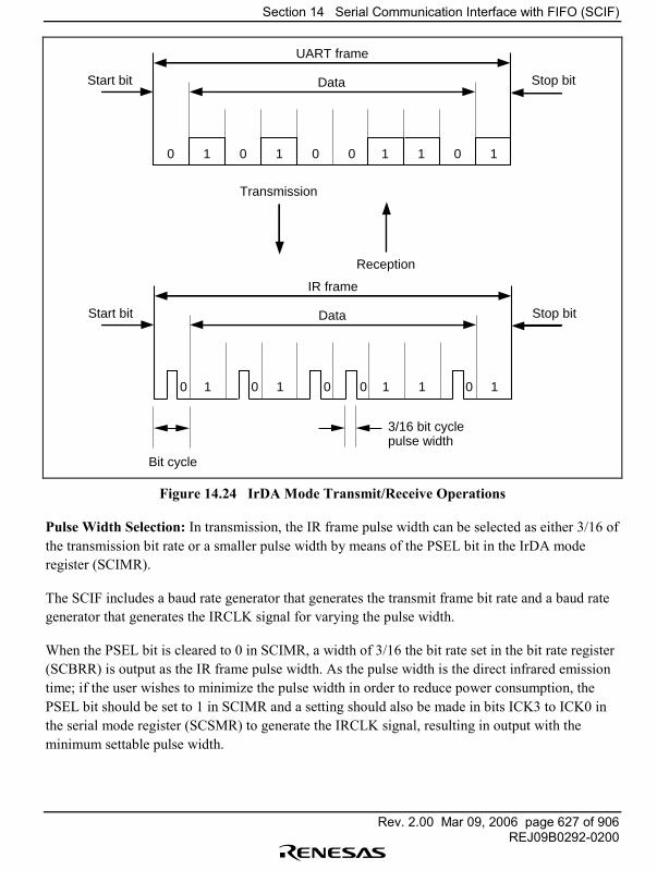
Section 14 Serial Communication Interface with FIFO (SCIF)
Rev. 2.00 Mar 09, 2006 page 627 of 906REJ09B0292-0200
0 1 0 1 0 0 1 1 0 1
UART frame
DataStart bit
Transmission
Reception
Stop bit
0 1 0 1 0 0 1 1 0 1
IR frame
DataStart bit
Bit cycle
Stop bit
3/16 bit cycle pulse width
Figure 14.24 IrDA Mode Transmit/Receive Operations
Pulse Width Selection: In transmission, the IR frame pulse width can be selected as either 3/16 ofthe transmission bit rate or a smaller pulse width by means of the PSEL bit in the IrDA moderegister (SCIMR).
The SCIF includes a baud rate generator that generates the transmit frame bit rate and a baud rategenerator that generates the IRCLK signal for varying the pulse width.
When the PSEL bit is cleared to 0 in SCIMR, a width of 3/16 the bit rate set in the bit rate register(SCBRR) is output as the IR frame pulse width. As the pulse width is the direct infrared emissiontime; if the user wishes to minimize the pulse width in order to reduce power consumption, thePSEL bit should be set to 1 in SCIMR and a setting should also be made in bits ICK3 to ICK0 inthe serial mode register (SCSMR) to generate the IRCLK signal, resulting in output with theminimum settable pulse width.
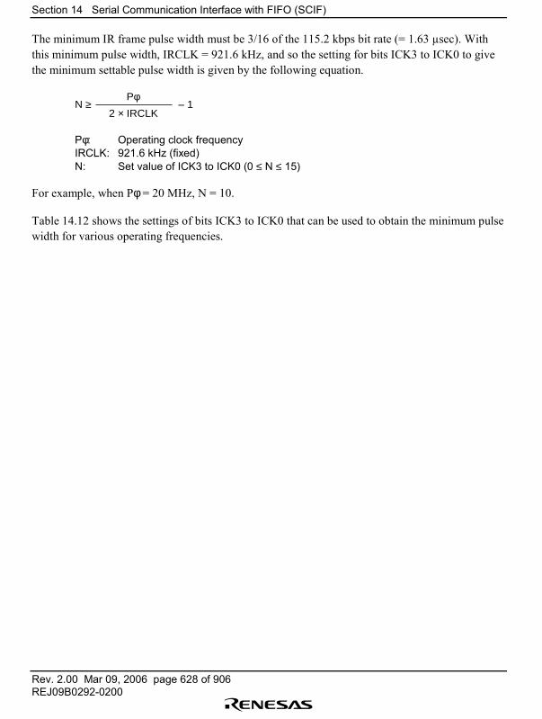
Section 14 Serial Communication Interface with FIFO (SCIF)
Rev. 2.00 Mar 09, 2006 page 628 of 906REJ09B0292-0200
The minimum IR frame pulse width must be 3/16 of the 115.2 kbps bit rate (= 1.63 µsec). Withthis minimum pulse width, IRCLK = 921.6 kHz, and so the setting for bits ICK3 to ICK0 to givethe minimum settable pulse width is given by the following equation.
N ≥2 × IRCLK
– 1Pφ
Pφ: Operating clock frequencyIRCLK: 921.6 kHz (fixed)N: Set value of ICK3 to ICK0 (0 ≤ N ≤ 15)
For example, when Pφ = 20 MHz, N = 10.
Table 14.12 shows the settings of bits ICK3 to ICK0 that can be used to obtain the minimum pulsewidth for various operating frequencies.
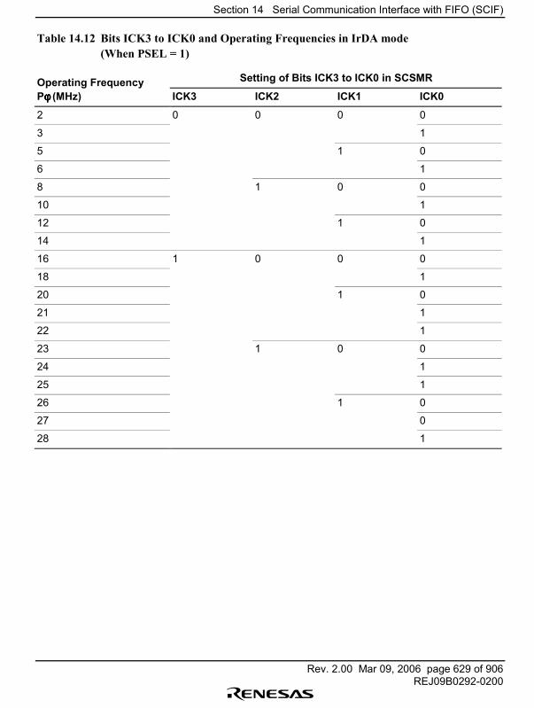
Section 14 Serial Communication Interface with FIFO (SCIF)
Rev. 2.00 Mar 09, 2006 page 629 of 906REJ09B0292-0200
Table 14.12 Bits ICK3 to ICK0 and Operating Frequencies in IrDA mode(When PSEL = 1)
Operating Frequency Setting of Bits ICK3 to ICK0 in SCSMR
Pφφφφ (MHz) ICK3 ICK2 ICK1 ICK0
2 0 0 0 0
3 1
5 1 0
6 1
8 1 0 0
10 1
12 1 0
14 1
16 1 0 0 0
18 1
20 1 0
21 1
22 1
23 1 0 0
24 1
25 1
26 1 0
27 0
28 1
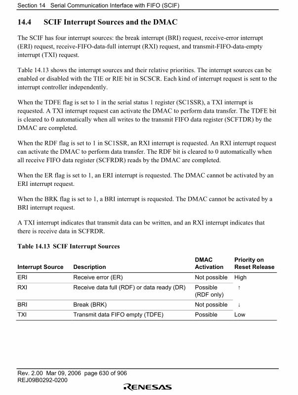
Section 14 Serial Communication Interface with FIFO (SCIF)
Rev. 2.00 Mar 09, 2006 page 630 of 906REJ09B0292-0200
14.4 SCIF Interrupt Sources and the DMAC
The SCIF has four interrupt sources: the break interrupt (BRI) request, receive-error interrupt(ERI) request, receive-FIFO-data-full interrupt (RXI) request, and transmit-FIFO-data-emptyinterrupt (TXI) request.
Table 14.13 shows the interrupt sources and their relative priorities. The interrupt sources can beenabled or disabled with the TIE or RIE bit in SCSCR. Each kind of interrupt request is sent to theinterrupt controller independently.
When the TDFE flag is set to 1 in the serial status 1 register (SC1SSR), a TXI interrupt isrequested. A TXI interrupt request can activate the DMAC to perform data transfer. The TDFE bitis cleared to 0 automatically when all writes to the transmit FIFO data register (SCFTDR) by theDMAC are completed.
When the RDF flag is set to 1 in SC1SSR, an RXI interrupt is requested. An RXI interrupt requestcan activate the DMAC to perform data transfer. The RDF bit is cleared to 0 automatically whenall receive FIFO data register (SCFRDR) reads by the DMAC are completed.
When the ER flag is set to 1, an ERI interrupt is requested. The DMAC cannot be activated by anERI interrupt request.
When the BRK flag is set to 1, a BRI interrupt is requested. The DMAC cannot be activated by aBRI interrupt request.
A TXI interrupt indicates that transmit data can be written, and an RXI interrupt indicates thatthere is receive data in SCFRDR.
Table 14.13 SCIF Interrupt Sources
Interrupt Source
Description
DMACActivation
Priority onReset Release
ERI Receive error (ER) Not possible High
RXI Receive data full (RDF) or data ready (DR) Possible(RDF only)
↑
BRI Break (BRK) Not possible ↓
TXI Transmit data FIFO empty (TDFE) Possible Low
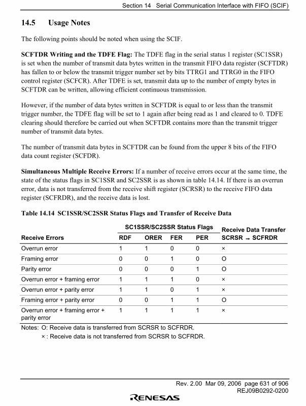
Section 14 Serial Communication Interface with FIFO (SCIF)
Rev. 2.00 Mar 09, 2006 page 631 of 906REJ09B0292-0200
14.5 Usage Notes
The following points should be noted when using the SCIF.
SCFTDR Writing and the TDFE Flag: The TDFE flag in the serial status 1 register (SC1SSR)is set when the number of transmit data bytes written in the transmit FIFO data register (SCFTDR)has fallen to or below the transmit trigger number set by bits TTRG1 and TTRG0 in the FIFOcontrol register (SCFCR). After TDFE is set, transmit data up to the number of empty bytes inSCFTDR can be written, allowing efficient continuous transmission.
However, if the number of data bytes written in SCFTDR is equal to or less than the transmittrigger number, the TDFE flag will be set to 1 again after being read as 1 and cleared to 0. TDFEclearing should therefore be carried out when SCFTDR contains more than the transmit triggernumber of transmit data bytes.
The number of transmit data bytes in SCFTDR can be found from the upper 8 bits of the FIFOdata count register (SCFDR).
Simultaneous Multiple Receive Errors: If a number of receive errors occur at the same time, thestate of the status flags in SC1SSR and SC2SSR is as shown in table 14.14. If there is an overrunerror, data is not transferred from the receive shift register (SCRSR) to the receive FIFO dataregister (SCFRDR), and the receive data is lost.
Table 14.14 SC1SSR/SC2SSR Status Flags and Transfer of Receive Data
SC1SSR/SC2SSR Status Flags Receive Data Transfer Receive Errors RDF ORER FER PER SCRSR →→→→ SCFRDR
Overrun error 1 1 0 0 × Framing error 0 0 1 0 O Parity error 0 0 0 1 O Overrun error + framing error 1 1 1 0 × Overrun error + parity error 1 1 0 1 × Framing error + parity error 0 0 1 1 O Overrun error + framing error +parity error
1 1 1 1 ×
Notes: O: Receive data is transferred from SCRSR to SCFRDR.× : Receive data is not transferred from SCRSR to SCFRDR.
Section 14 Serial Communication Interface with FIFO (SCIF)
Rev. 2.00 Mar 09, 2006 page 632 of 906REJ09B0292-0200
Break Detection and Processing: Break signals can be detected by reading the RxD pin directlywhen a framing error (FER) is detected. In the break state the input from the RxD pin consists ofall 0s, so the FER flag is set and the parity error flag (PER) may also be set.
Note that although the SCIF stops transferring receive data to SCFRDR after receiving a break, thereceive operation continues, so if the FER and BRK flags are cleared to 0 they will be set to 1again.
Sending a Break Signal: The TxD pin is a general I/O pin whose input/output direction and levelare determined by the I/O port data register (DR) and the control register (CR) of the pin functioncontroller (PFC). This fact can be used to send a break signal.
The DR value substitutes for the mark state until the PFC setting is made. The initial settingshould therefore be as an output port outputting 1.
To send a break signal during serial transmission, clear DR, then set the TxD pin as an output portwith the PFC.
When the TE bit is cleared to 0, the transmitter is initialized regardless of the current transmissionstate.
Receive Error Flags and Transmit Operations (Synchronous Mode Only): Transmissioncannot be started when any of the receive error flags (ORER, PER3 to PER0, FER3 to FER0) isset to 1, even if the TDFE flag is set to 1. Be sure to clear the receive error flags to 0 beforestarting transmission.
Note also that the receive error flags are not cleared to 0 by clearing the RE bit to 0.
Receive Data Sampling Timing and Receive Margin in Asynchronous Mode: In asynchronousmode, the SCIF operates on a base clock with a frequency of 16, 8, or 4 times the transfer rate.
In reception, the SCIF synchronizes internally with the fall of the start bit, which it samples on thebase clock. Receive data is latched at the rising edge of the eighth, fourth, or second base clockpulse. The timing is shown in figure 14.25.
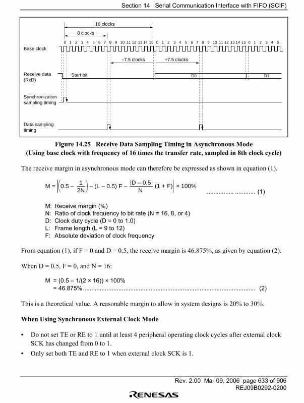
Section 14 Serial Communication Interface with FIFO (SCIF)
Rev. 2.00 Mar 09, 2006 page 633 of 906REJ09B0292-0200
0 1 2 3 4 5 6 7 8 9 10 11 12 13 14 15 0 1 2 3 4 5 6 7 8 9 10 11 12 13 14 15 0 1 2 3 4 5
Base clock
16 clocks
8 clocks
–7.5 clocks +7.5 clocks
Start bit D0 D1Receive data (RxD)
Synchronization sampling timing
Data sampling timing
Figure 14.25 Receive Data Sampling Timing in Asynchronous Mode(Using base clock with frequency of 16 times the transfer rate, sampled in 8th clock cycle)
The receive margin in asynchronous mode can therefore be expressed as shown in equation (1).
M = 0.5 – 1
2N D – 0.5
N– (L – 0.5) F – (1 + F) × 100%
................. ............ (1)
M: Receive margin (%)N: Ratio of clock frequency to bit rate (N = 16, 8, or 4)D: Clock duty cycle (D = 0 to 1.0)L: Frame length (L = 9 to 12)F: Absolute deviation of clock frequency
From equation (1), if F = 0 and D = 0.5, the receive margin is 46.875%, as given by equation (2).
When D = 0.5, F = 0, and N = 16:
M = (0.5 � 1/(2 × 16)) × 100%= 46.875%...................................................................................................... (2)
This is a theoretical value. A reasonable margin to allow in system designs is 20% to 30%.
When Using Synchronous External Clock Mode
• Do not set TE or RE to 1 until at least 4 peripheral operating clock cycles after external clockSCK has changed from 0 to 1.
• Only set both TE and RE to 1 when external clock SCK is 1.
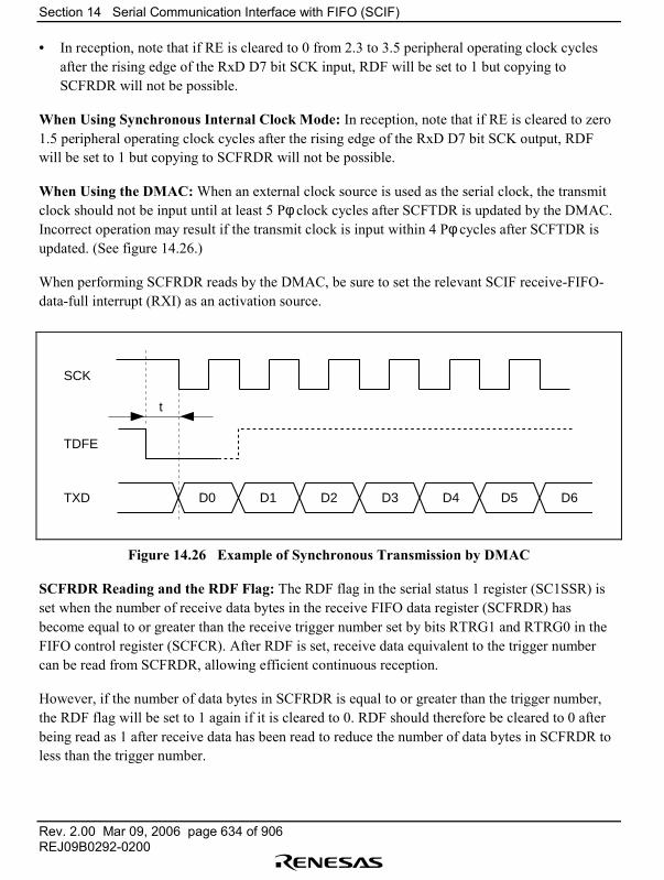
Section 14 Serial Communication Interface with FIFO (SCIF)
Rev. 2.00 Mar 09, 2006 page 634 of 906REJ09B0292-0200
• In reception, note that if RE is cleared to 0 from 2.3 to 3.5 peripheral operating clock cyclesafter the rising edge of the RxD D7 bit SCK input, RDF will be set to 1 but copying toSCFRDR will not be possible.
When Using Synchronous Internal Clock Mode: In reception, note that if RE is cleared to zero1.5 peripheral operating clock cycles after the rising edge of the RxD D7 bit SCK output, RDFwill be set to 1 but copying to SCFRDR will not be possible.
When Using the DMAC: When an external clock source is used as the serial clock, the transmitclock should not be input until at least 5 Pφ clock cycles after SCFTDR is updated by the DMAC.Incorrect operation may result if the transmit clock is input within 4 Pφ cycles after SCFTDR isupdated. (See figure 14.26.)
When performing SCFRDR reads by the DMAC, be sure to set the relevant SCIF receive-FIFO-data-full interrupt (RXI) as an activation source.
SCK
TDFE
TXD D0 D1 D2 D3 D4 D5 D6
t
Figure 14.26 Example of Synchronous Transmission by DMAC
SCFRDR Reading and the RDF Flag: The RDF flag in the serial status 1 register (SC1SSR) isset when the number of receive data bytes in the receive FIFO data register (SCFRDR) hasbecome equal to or greater than the receive trigger number set by bits RTRG1 and RTRG0 in theFIFO control register (SCFCR). After RDF is set, receive data equivalent to the trigger numbercan be read from SCFRDR, allowing efficient continuous reception.
However, if the number of data bytes in SCFRDR is equal to or greater than the trigger number,the RDF flag will be set to 1 again if it is cleared to 0. RDF should therefore be cleared to 0 afterbeing read as 1 after receive data has been read to reduce the number of data bytes in SCFRDR toless than the trigger number.
Section 14 Serial Communication Interface with FIFO (SCIF)
Rev. 2.00 Mar 09, 2006 page 635 of 906REJ09B0292-0200
The number of receive data bytes in SCFRDR can be found from the lower 8 bits of the FIFO datacount register (SCFDR).
SCFRDR Reading when Overrun Occurs: If a receive operation is continued despite the factthat the receive FIFO data register (SCFRDR) contains 16 bytes of data, overrun will occur.
If SCFRDR is read in this state, the data that caused the overrun is read in the 17th read. The valuereturned in the 18th and subsequent reads will be undefined.
Also note that, from the first SCFRDR read onward, the number of receive data bytes in SCFRDRindicated by the lower 8 bits of the FIFO data count register (SCFDR) is one more than the actualnumber of receive data bytes.
Section 14 Serial Communication Interface with FIFO (SCIF)
Rev. 2.00 Mar 09, 2006 page 636 of 906REJ09B0292-0200
Section 15 Serial I/O with FIFO (SIOF)
Rev. 2.00 Mar 09, 2006 page 637 of 906REJ09B0292-0200
Section 15 Serial I/O with FIFO (SIOF)
15.1 Overview
The serial I/O with FIFO functions mainly as an interface between the chip and a codec or modemanalog front-end.
15.1.1 Features
The serial I/O has the following features:
• Full-duplex operationIndependent transmit/receive registers and independent transmit/receive clocks
• Primary data transmit/receive FIFO/Double-buffered transmit/receive portsContinuous data transmission/reception possible
• Interval transfer mode and continuous transfer mode• Memory-mapped receive data register, transmit data register, serial control register, and serial
status register, receive control data register, transmit control data register, FIFO controlregister, FIFO data count registerWith the exception of SIRSR and SITSR, these registers are memory-mapped and can beaccessed by a MOV instruction.
• Choice of 8- or 16-bit data length• Data transfer communication by means of polling or interrupts
Data transfer can be monitored by polling the receive data register full flag (RDRF), thereceive data register empty flag (RDRE), the receive control data register full flag (RCD), andthe transmit control data register empty flag (TCD). Interrupt requests can be generated duringdata transfer by setting the receive interrupt request flag and the transmit interrupt request flag.
• Either MSB-first or LSB transfer can be selected for data I/O operations.
Figure 15.1 shows a block diagram of the serial I/O with FIFO.
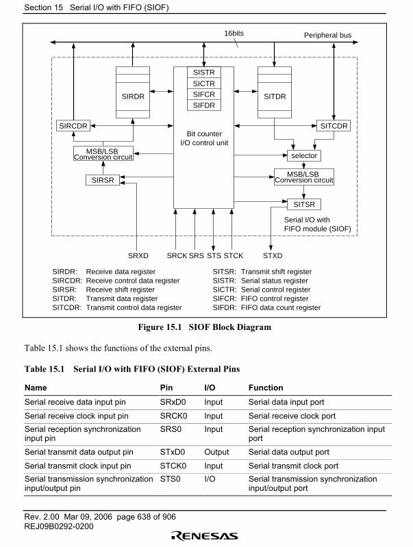
Section 15 Serial I/O with FIFO (SIOF)
Rev. 2.00 Mar 09, 2006 page 638 of 906REJ09B0292-0200
16bits
SIRCDR
SISTR
SICTR
SIRDR SIFCR
SIFDR
STCKSRCKSRXD
SIRDR:SIRCDR:SIRSR:SITDR:SITCDR:
SIRSR
STXDSRS STS
MSB/LSB Conversion circuit
SITCDR
SITDR
SITSR
selector
MSB/LSB Conversion circuit
Peripheral bus
Receive data registerReceive control data registerReceive shift registerTransmit data registerTransmit control data register
SITSR:SISTR:SICTR:SIFCR:SIFDR:
Transmit shift registerSerial status registerSerial control registerFIFO control registerFIFO data count register
Bit counterI/O control unit
Serial I/O with FIFO module (SIOF)
Figure 15.1 SIOF Block Diagram
Table 15.1 shows the functions of the external pins.
Table 15.1 Serial I/O with FIFO (SIOF) External Pins
Name Pin I/O Function
Serial receive data input pin SRxD0 Input Serial data input port
Serial receive clock input pin SRCK0 Input Serial receive clock portSerial reception synchronizationinput pin
SRS0 Input Serial reception synchronization inputport
Serial transmit data output pin STxD0 Output Serial data output port
Serial transmit clock input pin STCK0 Input Serial transmit clock portSerial transmission synchronizationinput/output pin
STS0 I/O Serial transmission synchronizationinput/output port
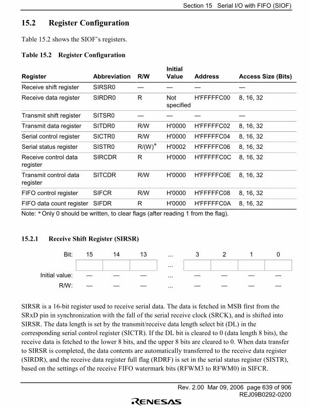
Section 15 Serial I/O with FIFO (SIOF)
Rev. 2.00 Mar 09, 2006 page 639 of 906REJ09B0292-0200
15.2 Register Configuration
Table 15.2 shows the SIOF�s registers.
Table 15.2 Register Configuration
Register Abbreviation R/WInitialValue Address Access Size (Bits)
Receive shift register SIRSR0 � � � �
Receive data register SIRDR0 R Notspecified
H'FFFFFC00 8, 16, 32
Transmit shift register SITSR0 � � � �
Transmit data register SITDR0 R/W H'0000 H'FFFFFC02 8, 16, 32
Serial control register SICTR0 R/W H'0000 H'FFFFFC04 8, 16, 32
Serial status register SISTR0 R/(W)* H'0002 H'FFFFFC06 8, 16, 32
Receive control dataregister
SIRCDR R H'0000 H'FFFFFC0C 8, 16, 32
Transmit control dataregister
SITCDR R/W H'0000 H'FFFFFC0E 8, 16, 32
FIFO control register SIFCR R/W H'0000 H'FFFFFC08 8, 16, 32
FIFO data count register SIFDR R H'0000 H'FFFFFC0A 8, 16, 32Note: * Only 0 should be written, to clear flags (after reading 1 from the flag).
15.2.1 Receive Shift Register (SIRSR)
Bit: 15 14 13 ... 3 2 1 0
...
Initial value: � � � ... � � � �
R/W: � � � ... � � � �
SIRSR is a 16-bit register used to receive serial data. The data is fetched in MSB first from theSRxD pin in synchronization with the fall of the serial receive clock (SRCK), and is shifted intoSIRSR. The data length is set by the transmit/receive data length select bit (DL) in thecorresponding serial control register (SICTR). If the DL bit is cleared to 0 (data length 8 bits), thereceive data is fetched to the lower 8 bits, and the upper 8 bits are cleared to 0. When data transferto SIRSR is completed, the data contents are automatically transferred to the receive data register(SIRDR), and the receive data register full flag (RDRF) is set in the serial status register (SISTR),based on the settings of the receive FIFO watermark bits (RFWM3 to RFWM0) in SIFCR.
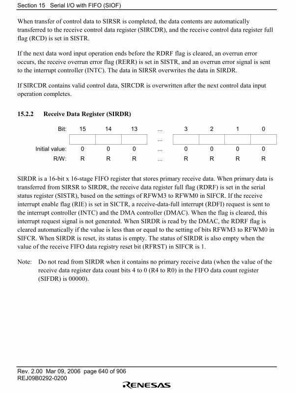
Section 15 Serial I/O with FIFO (SIOF)
Rev. 2.00 Mar 09, 2006 page 640 of 906REJ09B0292-0200
When transfer of control data to SIRSR is completed, the data contents are automaticallytransferred to the receive control data register (SIRCDR), and the receive control data register fullflag (RCD) is set in SISTR.
If the next data word input operation ends before the RDRF flag is cleared, an overrun erroroccurs, the receive overrun error flag (RERR) is set in SISTR, and an overrun error signal is sentto the interrupt controller (INTC). The data in SIRSR overwrites the data in SIRDR.
If SIRCDR contains valid control data, SIRCDR is overwritten after the next control data inputoperation completes.
15.2.2 Receive Data Register (SIRDR)
Bit: 15 14 13 ... 3 2 1 0
...
Initial value: 0 0 0 ... 0 0 0 0
R/W: R R R ... R R R R
SIRDR is a 16-bit x 16-stage FIFO register that stores primary receive data. When primary data istransferred from SIRSR to SIRDR, the receive data register full flag (RDRF) is set in the serialstatus register (SISTR), based on the settings of RFWM3 to RFWM0 in SIFCR. If the receiveinterrupt enable flag (RIE) is set in SICTR, a receive-data-full interrupt (RDFI) request is sent tothe interrupt controller (INTC) and the DMA controller (DMAC). When the flag is cleared, thisinterrupt request signal is not generated. When SIRDR is read by the DMAC, the RDRF flag iscleared automatically if the value is less than or equal to the setting of bits RFWM3 to RFWM0 inSIFCR. When SIRDR is reset, its status is empty. The status of SIRDR is also empty when thevalue of the receive FIFO data registry reset bit (RFRST) in SIFCR is 1.
Note: Do not read from SIRDR when it contains no primary receive data (when the value of thereceive data register data count bits 4 to 0 (R4 to R0) in the FIFO data count register(SIFDR) is 00000).
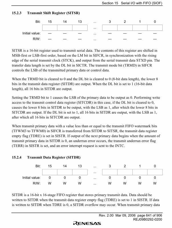
Section 15 Serial I/O with FIFO (SIOF)
Rev. 2.00 Mar 09, 2006 page 641 of 906REJ09B0292-0200
15.2.3 Transmit Shift Register (SITSR)
Bit: 15 14 13 ... 3 2 1 0
...
Initial value: � � � ... � � � �
R/W: � � � ... � � � �
SITSR is a 16-bit register used to transmit serial data. The contents of this register are shifted inMSB-first or LSB-first order, based on the LM bit in SIFCR, in synchronization with the risingedge of the serial transmit clock (STCK), and output from the serial transmit data STXD pin. Thetransfer data length is set by the DL bit in SICTR. The transmit mode bit (TRMD) in SIFCRcontrols the LSB of the transmitted primary data or control data.
When the TRMD bit is cleared to 0 and the DL bit is cleared to 0 (8-bit data length), the lower 8bits in the transmit data register (SITDR) are output. When the DL bit is set to 1 (16-bit datalength), all 16 bits in SITDR are output.
Setting the TRMD bit to 1 causes the LSB of the primary data to be output as 0. Performing writeaccess to the transmit control data register (SITCDR) in this case, if the DL bit is cleared to 0,causes the lower 8 bits in SITDR to be output, with the LSB as 1, after which the lower 8 bits inSITCDR are output. If the DL bit is set to 1, all 16 bits in SITDR are output, with the LSB as 1,after which all 16 bits in SITCDR are output.
When transmit primary data with a value less than or equal to the transmit FIFO watermark bits(TFWM3 to TFWM0) in SIFCR is transferred from SITDR to SITSR, the transmit data registerempty flag (TDRE) is set in SISTR. If output of the next primary data begins when the amount oftransmit primary data in SITDR is 0, an underrun error occurs, the transmit underrun error flag(TERR) in SISTR is set, and an error interrupt request is sent to the INTC.
15.2.4 Transmit Data Register (SITDR)
Bit: 15 14 13 ... 3 2 1 0
...
Initial value: 0 0 0 ... 0 0 0 0
R/W: W W W ... W W W W
SITDR is a 16-bit x 16-stage FIFO register that stores primary transmit data. Data should bewritten to SITDR when the transmit data register empty flag (TDRE) is set to 1 in SISTR. If datais written to SITDR when TDRE is 0, a SITDR overflow may occur. When transmit primary data
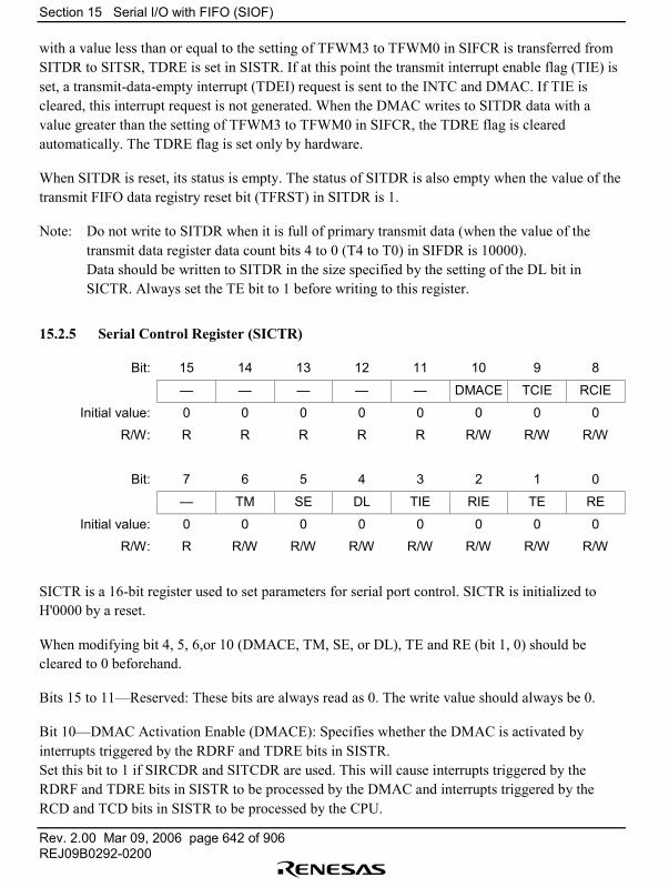
Section 15 Serial I/O with FIFO (SIOF)
Rev. 2.00 Mar 09, 2006 page 642 of 906REJ09B0292-0200
with a value less than or equal to the setting of TFWM3 to TFWM0 in SIFCR is transferred fromSITDR to SITSR, TDRE is set in SISTR. If at this point the transmit interrupt enable flag (TIE) isset, a transmit-data-empty interrupt (TDEI) request is sent to the INTC and DMAC. If TIE iscleared, this interrupt request is not generated. When the DMAC writes to SITDR data with avalue greater than the setting of TFWM3 to TFWM0 in SIFCR, the TDRE flag is clearedautomatically. The TDRE flag is set only by hardware.
When SITDR is reset, its status is empty. The status of SITDR is also empty when the value of thetransmit FIFO data registry reset bit (TFRST) in SITDR is 1.
Note: Do not write to SITDR when it is full of primary transmit data (when the value of thetransmit data register data count bits 4 to 0 (T4 to T0) in SIFDR is 10000).Data should be written to SITDR in the size specified by the setting of the DL bit inSICTR. Always set the TE bit to 1 before writing to this register.
15.2.5 Serial Control Register (SICTR)
Bit: 15 14 13 12 11 10 9 8
� � � � � DMACE TCIE RCIE
Initial value: 0 0 0 0 0 0 0 0
R/W: R R R R R R/W R/W R/W
Bit: 7 6 5 4 3 2 1 0
� TM SE DL TIE RIE TE RE
Initial value: 0 0 0 0 0 0 0 0
R/W: R R/W R/W R/W R/W R/W R/W R/W
SICTR is a 16-bit register used to set parameters for serial port control. SICTR is initialized toH'0000 by a reset.
When modifying bit 4, 5, 6,or 10 (DMACE, TM, SE, or DL), TE and RE (bit 1, 0) should becleared to 0 beforehand.
Bits 15 to 11�Reserved: These bits are always read as 0. The write value should always be 0.
Bit 10�DMAC Activation Enable (DMACE): Specifies whether the DMAC is activated byinterrupts triggered by the RDRF and TDRE bits in SISTR.Set this bit to 1 if SIRCDR and SITCDR are used. This will cause interrupts triggered by theRDRF and TDRE bits in SISTR to be processed by the DMAC and interrupts triggered by theRCD and TCD bits in SISTR to be processed by the CPU.
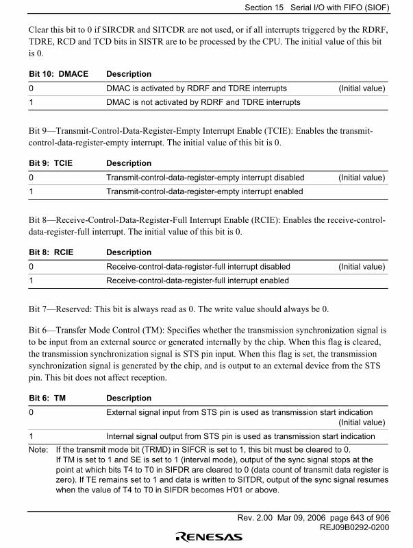
Section 15 Serial I/O with FIFO (SIOF)
Rev. 2.00 Mar 09, 2006 page 643 of 906REJ09B0292-0200
Clear this bit to 0 if SIRCDR and SITCDR are not used, or if all interrupts triggered by the RDRF,TDRE, RCD and TCD bits in SISTR are to be processed by the CPU. The initial value of this bitis 0.
Bit 10: DMACE Description
0 DMAC is activated by RDRF and TDRE interrupts (Initial value)
1 DMAC is not activated by RDRF and TDRE interrupts
Bit 9�Transmit-Control-Data-Register-Empty Interrupt Enable (TCIE): Enables the transmit-control-data-register-empty interrupt. The initial value of this bit is 0.
Bit 9: TCIE Description
0 Transmit-control-data-register-empty interrupt disabled (Initial value)
1 Transmit-control-data-register-empty interrupt enabled
Bit 8�Receive-Control-Data-Register-Full Interrupt Enable (RCIE): Enables the receive-control-data-register-full interrupt. The initial value of this bit is 0.
Bit 8: RCIE Description
0 Receive-control-data-register-full interrupt disabled (Initial value)
1 Receive-control-data-register-full interrupt enabled
Bit 7�Reserved: This bit is always read as 0. The write value should always be 0.
Bit 6�Transfer Mode Control (TM): Specifies whether the transmission synchronization signal isto be input from an external source or generated internally by the chip. When this flag is cleared,the transmission synchronization signal is STS pin input. When this flag is set, the transmissionsynchronization signal is generated by the chip, and is output to an external device from the STSpin. This bit does not affect reception.
Bit 6: TM Description
0 External signal input from STS pin is used as transmission start indication(Initial value)
1 Internal signal output from STS pin is used as transmission start indicationNote: If the transmit mode bit (TRMD) in SIFCR is set to 1, this bit must be cleared to 0.
If TM is set to 1 and SE is set to 1 (interval mode), output of the sync signal stops at thepoint at which bits T4 to T0 in SIFDR are cleared to 0 (data count of transmit data register iszero). If TE remains set to 1 and data is written to SITDR, output of the sync signal resumeswhen the value of T4 to T0 in SIFDR becomes H'01 or above.
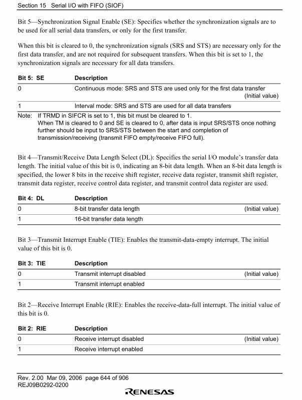
Section 15 Serial I/O with FIFO (SIOF)
Rev. 2.00 Mar 09, 2006 page 644 of 906REJ09B0292-0200
Bit 5�Synchronization Signal Enable (SE): Specifies whether the synchronization signals are tobe used for all serial data transfers, or only for the first transfer.
When this bit is cleared to 0, the synchronization signals (SRS and STS) are necessary only for thefirst data transfer, and are not required for subsequent transfers. When this bit is set to 1, thesynchronization signals are necessary for all data transfers.
Bit 5: SE Description
0 Continuous mode: SRS and STS are used only for the first data transfer(Initial value)
1 Interval mode: SRS and STS are used for all data transfersNote: If TRMD in SIFCR is set to 1, this bit must be cleared to 1.
When TM is cleared to 0 and SE is cleared to 0, after data is input SRS/STS once nothingfurther should be input to SRS/STS between the start and completion oftransmission/receiving (transmit FIFO empty/receive FIFO full).
Bit 4�Transmit/Receive Data Length Select (DL): Specifies the serial I/O module�s transfer datalength. The initial value of this bit is 0, indicating an 8-bit data length. When an 8-bit data length isspecified, the lower 8 bits in the receive shift register, receive data register, transmit shift register,transmit data register, receive control data register, and transmit control data register are used.
Bit 4: DL Description
0 8-bit transfer data length (Initial value)
1 16-bit transfer data length
Bit 3�Transmit Interrupt Enable (TIE): Enables the transmit-data-empty interrupt. The initialvalue of this bit is 0.
Bit 3: TIE Description
0 Transmit interrupt disabled (Initial value)
1 Transmit interrupt enabled
Bit 2�Receive Interrupt Enable (RIE): Enables the receive-data-full interrupt. The initial value ofthis bit is 0.
Bit 2: RIE Description
0 Receive interrupt disabled (Initial value)
1 Receive interrupt enabled
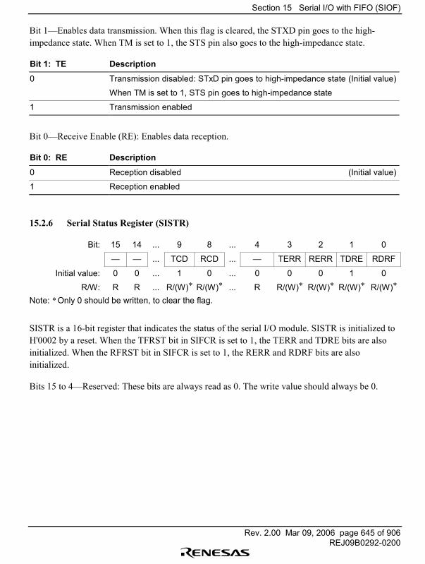
Section 15 Serial I/O with FIFO (SIOF)
Rev. 2.00 Mar 09, 2006 page 645 of 906REJ09B0292-0200
Bit 1�Enables data transmission. When this flag is cleared, the STXD pin goes to the high-impedance state. When TM is set to 1, the STS pin also goes to the high-impedance state.
Bit 1: TE Description
0 Transmission disabled: STxD pin goes to high-impedance state (Initial value)
When TM is set to 1, STS pin goes to high-impedance state
1 Transmission enabled
Bit 0�Receive Enable (RE): Enables data reception.
Bit 0: RE Description
0 Reception disabled (Initial value)
1 Reception enabled
15.2.6 Serial Status Register (SISTR)
Bit: 15 14 ... 9 8 ... 4 3 2 1 0
� � ... TCD RCD ... � TERR RERR TDRE RDRF
Initial value: 0 0 ... 1 0 ... 0 0 0 1 0
R/W: R R ... R/(W)* R/(W)* ... R R/(W)* R/(W)* R/(W)* R/(W)*
Note: * Only 0 should be written, to clear the flag.
SISTR is a 16-bit register that indicates the status of the serial I/O module. SISTR is initialized toH'0002 by a reset. When the TFRST bit in SIFCR is set to 1, the TERR and TDRE bits are alsoinitialized. When the RFRST bit in SIFCR is set to 1, the RERR and RDRF bits are alsoinitialized.
Bits 15 to 4�Reserved: These bits are always read as 0. The write value should always be 0.

Section 15 Serial I/O with FIFO (SIOF)
Rev. 2.00 Mar 09, 2006 page 646 of 906REJ09B0292-0200
Bit 9�Transmit Control Data Register Empty (TCD): This flag indicates when SITCDR is emptyand can be written to.
Bit 9: TCD Description
0 SITCDR transmit data is validTCD is cleared to 0 in the following cases:
• When 0 is written to TCD after reading TCD = 11 SITCDR transmit data is invalid (Initial value)
TCD is set to 1 in the following cases:
• After data is transferred from SITCDR to SITSR
• When the processor is reset
Bit 8�Receive Control Data Register Full (RCD): This flag indicates when SIRCDR is in waitstatus.
Bit 8: RCD Description
0 SIRCDR receive data is invalid (Initial value)RCD is cleared to 0 in the following cases:
• When 0 is written to RCD after reading RCD = 1
• When the processor is reset1 SIRCDR transmit data is valid
RCD is set to 1 in the following cases:
• After control data has been received normally and data has beentransferred from SIRSR to SIRCDR
Bit 7 to 4�Reserved: This bit is always read as 0. The write value should always be 0.
Bit 3�Transmit Underrun Error (TERR): Flag that indicates the occurrence of a transmitunderrun.
Bit 3: TERR Description0 Transmission is in progress, or has ended normally (Initial value)
[Clearing conditions]• When 0 is written to the TERR bit after reading TERR = 1• When the TFRST bit in SIFCR is set to 1• When the processor enters the reset state
1 A transmit underrun error has occurred• When the amount of primary transmit data in SITDR is 0 and data is
transferred from SITDR to SITSR using a transmit operation
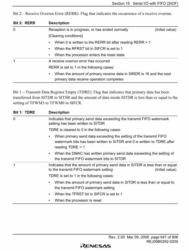
Section 15 Serial I/O with FIFO (SIOF)
Rev. 2.00 Mar 09, 2006 page 647 of 906REJ09B0292-0200
Bit 2�Receive Overrun Error (RERR): Flag that indicates the occurrence of a receive overrun.
Bit 2: RERR Description
0 Reception is in progress, or has ended normally (Initial value)
[Clearing conditions]
• When 0 is written to the RERR bit after reading RERR = 1
• When the RFRST bit in SIFCR is set to 1
• When the processor enters the reset state1 A receive overrun error has occurred
RERR is set to 1 in the following cases:
• When the amount of primary receive data in SIRDR is 16 and the nextprimary data receive operation completes
Bit 1�Transmit Data Register Empty (TDRE): Flag that indicates that primary data has beentransferred from SITDR to SITSR and the amount of data inside SITDR is less than or equal to thesetting of TFWM3 to TFWM0 in SIFCR.
Bit 1: TDRE Description
0 Indicates that primary send data exceeding the transmit FIFO watermarksetting has been written to SITDR
TDRE is cleared to 0 in the following cases:
• When primary send data exceeding the setting of the transmit FIFOwatermark bits has been written to SITDR and 0 is written to TDRE afterreading TDRE = 1
• When the DMAC has written primary send data exceeding the setting ofthe transmit FIFO watermark bits to SITDR
1 Indicates that the amount of primary send data in SITDR is less than or equalto the transmit FIFO watermark setting (Initial value)
TDRE is set to 1 in the following cases:
• When the amount of primary send data in SITDR is less than or equal tothe transmit FIFO watermark setting
• When the TFRST bit in SIFCR is set to 1
• When the processor is reset
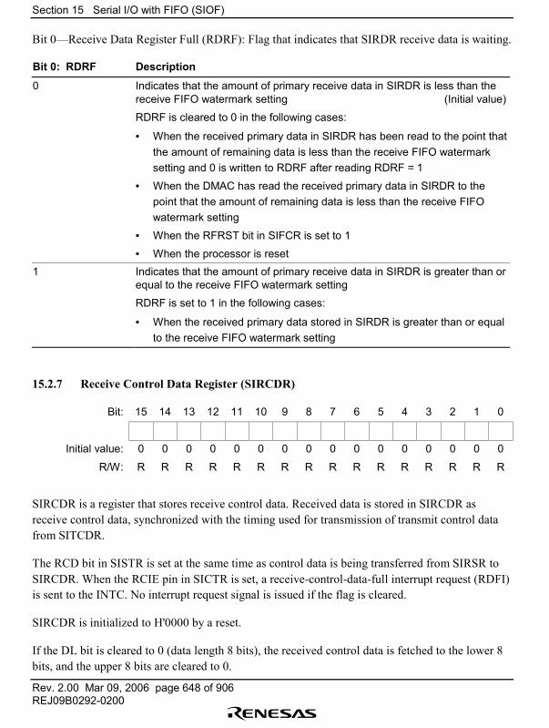
Section 15 Serial I/O with FIFO (SIOF)
Rev. 2.00 Mar 09, 2006 page 648 of 906REJ09B0292-0200
Bit 0�Receive Data Register Full (RDRF): Flag that indicates that SIRDR receive data is waiting.
Bit 0: RDRF Description
0 Indicates that the amount of primary receive data in SIRDR is less than thereceive FIFO watermark setting (Initial value)
RDRF is cleared to 0 in the following cases:
• When the received primary data in SIRDR has been read to the point thatthe amount of remaining data is less than the receive FIFO watermarksetting and 0 is written to RDRF after reading RDRF = 1
• When the DMAC has read the received primary data in SIRDR to thepoint that the amount of remaining data is less than the receive FIFOwatermark setting
• When the RFRST bit in SIFCR is set to 1
• When the processor is reset1 Indicates that the amount of primary receive data in SIRDR is greater than or
equal to the receive FIFO watermark setting
RDRF is set to 1 in the following cases:
• When the received primary data stored in SIRDR is greater than or equalto the receive FIFO watermark setting
15.2.7 Receive Control Data Register (SIRCDR)
Bit: 15 14 13 12 11 10 9 8 7 6 5 4 3 2 1 0
Initial value: 0 0 0 0 0 0 0 0 0 0 0 0 0 0 0 0
R/W: R R R R R R R R R R R R R R R R
SIRCDR is a register that stores receive control data. Received data is stored in SIRCDR asreceive control data, synchronized with the timing used for transmission of transmit control datafrom SITCDR.
The RCD bit in SISTR is set at the same time as control data is being transferred from SIRSR toSIRCDR. When the RCIE pin in SICTR is set, a receive-control-data-full interrupt request (RDFI)is sent to the INTC. No interrupt request signal is issued if the flag is cleared.
SIRCDR is initialized to H'0000 by a reset.
If the DL bit is cleared to 0 (data length 8 bits), the received control data is fetched to the lower 8bits, and the upper 8 bits are cleared to 0.
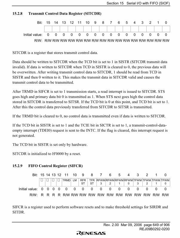
Section 15 Serial I/O with FIFO (SIOF)
Rev. 2.00 Mar 09, 2006 page 649 of 906REJ09B0292-0200
15.2.8 Transmit Control Data Register (SITCDR)
Bit: 15 14 13 12 11 10 9 8 7 6 5 4 3 2 1 0
Initial value: 0 0 0 0 0 0 0 0 0 0 0 0 0 0 0 0
R/W: R/W R/W R/W R/W R/W R/W R/W R/W R/W R/W R/W R/W R/W R/W R/W R/W
SITCDR is a register that stores transmit control data.
Data should be written to SITCDR when the TCD bit is set to 1 in SISTR (SITCDR transmit datainvalid). If data is written to SITCDR when TCD in SISTR is cleared to 0, the previous data willbe overwritten. After writing transmit control data to SITCDR, 1 should be read from TCD inSISTR and then 0 written to it. This makes the transmit data in SITCDR valid and causes thetransmit control data to be transmitted.
After TRMD in SIFCR is set to 1 transmission starts, a read interrupt is issued to SITCDR. STSgoes high and primary data bit 0 is transmitted as 1. When STS next goes high the control datastored in SITCDR is transferred to SITSR. If the TCD bit is 0 at this point, and TCD bit is set to 1.After this the control data previously transferred from SITCDR to SITSR is transmitted.
If the TRMD bit is cleared to 0, no control data is transmitted even if data is written to SITCDR.
If the TCD bit in SISTR is set to 1 and the TCIE bit in SICTR is set to 1, a transmit-control-data-empty interrupt (TDEI0) request is sent to the INTC. If the flag is cleared, this interrupt request isnot generated.
The TCD bit in SISTR is set only by hardware.
SITCDR is initialized to H'0000 by a reset.
15.2.9 FIFO Control Register (SIFCR)
Bit: 15 14 13 12 11 10 9 8 7 6 5 4 3 2 1 0 TRMD LM RFR
STTFRST
RFWM3
RFWM2
RFWM1
RFWM0
TFWM3
TFWM2
TFWM1
TFWM0
Initial value: 0 0 0 0 0 0 0 0 0 0 0 0 0 0 0 0
R/W: R R R R R/W R/W R/W R/W R/W R/W R/W R/W R/W R/W R/W R/W
SIFCR is a register used to perform software resets and to make threshold settings for SIRDR andSITDR.
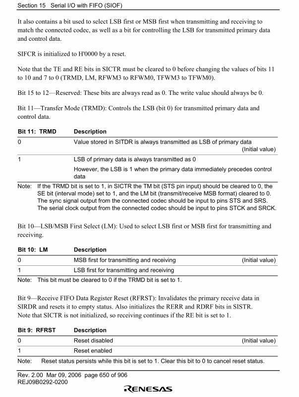
Section 15 Serial I/O with FIFO (SIOF)
Rev. 2.00 Mar 09, 2006 page 650 of 906REJ09B0292-0200
It also contains a bit used to select LSB first or MSB first when transmitting and receiving tomatch the connected codec, as well as a bit for controlling the LSB for transmitted primary dataand control data.
SIFCR is initialized to H'0000 by a reset.
Note that the TE and RE bits in SICTR must be cleared to 0 before changing the values of bits 11to 10 and 7 to 0 (TRMD, LM, RFWM3 to RFWM0, TFWM3 to TFWM0).
Bit 15 to 12�Reserved: These bits are always read as 0. The write value should always be 0.
Bit 11�Transfer Mode (TRMD): Controls the LSB (bit 0) for transmitted primary data andcontrol data.
Bit 11: TRMD Description
0 Value stored in SITDR is always transmitted as LSB of primary data(Initial value)
1 LSB of primary data is always transmitted as 0
However, the LSB is 1 when the primary data immediately precedes controldata
Note: If the TRMD bit is set to 1, in SICTR the TM bit (STS pin input) should be cleared to 0, theSE bit (interval mode) set to 1, and the LM bit (transmit/receive MSB format) cleared to 0.The sync signal output from the connected codec should be input to pins STS and SRS.The serial clock output from the connected codec should be input to pins STCK and SRCK.
Bit 10�LSB/MSB First Select (LM): Used to select LSB first or MSB first for transmitting andreceiving.
Bit 10: LM Description
0 MSB first for transmitting and receiving (Initial value)
1 LSB first for transmitting and receivingNote: This bit must be cleared to 0 if the TRMD bit is set to 1.
Bit 9�Receive FIFO Data Register Reset (RFRST): Invalidates the primary receive data inSIRDR and resets it to empty status. Also initializes the RERR and RDRF bits in SISTR.Note that SICTR is not initialized, so receiving continues if the RE bit is set to 1.
Bit 9: RFRST Description
0 Reset disabled (Initial value)
1 Reset enabled
Note: Reset status persists while this bit is set to 1. Clear this bit to 0 to cancel reset status.
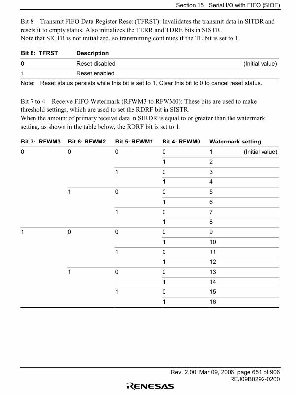
Section 15 Serial I/O with FIFO (SIOF)
Rev. 2.00 Mar 09, 2006 page 651 of 906REJ09B0292-0200
Bit 8�Transmit FIFO Data Register Reset (TFRST): Invalidates the transmit data in SITDR andresets it to empty status. Also initializes the TERR and TDRE bits in SISTR.Note that SICTR is not initialized, so transmitting continues if the TE bit is set to 1.
Bit 8: TFRST Description
0 Reset disabled (Initial value)
1 Reset enabledNote: Reset status persists while this bit is set to 1. Clear this bit to 0 to cancel reset status.
Bit 7 to 4�Receive FIFO Watermark (RFWM3 to RFWM0): These bits are used to makethreshold settings, which are used to set the RDRF bit in SISTR.When the amount of primary receive data in SIRDR is equal to or greater than the watermarksetting, as shown in the table below, the RDRF bit is set to 1.
Bit 7: RFWM3 Bit 6: RFWM2 Bit 5: RFWM1 Bit 4: RFWM0 Watermark setting
0 0 0 0 1 (Initial value)
1 2
1 0 3
1 4
1 0 0 5
1 6
1 0 7
1 8
1 0 0 0 9
1 10
1 0 11
1 12
1 0 0 13
1 14
1 0 15
1 16
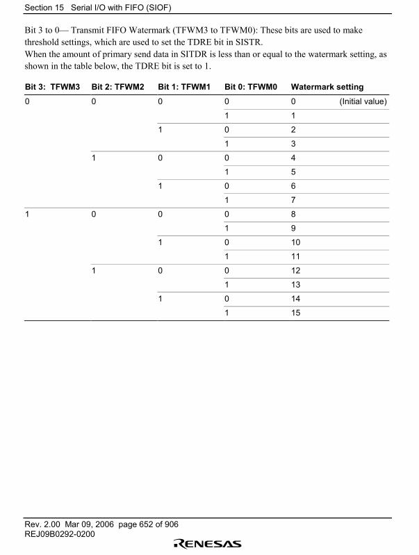
Section 15 Serial I/O with FIFO (SIOF)
Rev. 2.00 Mar 09, 2006 page 652 of 906REJ09B0292-0200
Bit 3 to 0� Transmit FIFO Watermark (TFWM3 to TFWM0): These bits are used to makethreshold settings, which are used to set the TDRE bit in SISTR.When the amount of primary send data in SITDR is less than or equal to the watermark setting, asshown in the table below, the TDRE bit is set to 1.
Bit 3: TFWM3 Bit 2: TFWM2 Bit 1: TFWM1 Bit 0: TFWM0 Watermark setting
0 0 0 0 0 (Initial value)
1 1
1 0 2
1 3
1 0 0 4
1 5
1 0 6
1 7
1 0 0 0 8
1 9
1 0 10
1 11
1 0 0 12
1 13
1 0 14
1 15

Section 15 Serial I/O with FIFO (SIOF)
Rev. 2.00 Mar 09, 2006 page 653 of 906REJ09B0292-0200
15.2.10 FIFO Data Count Register (SIFDR)
Bit: 15 14 13 12 11 10 9 8 7 6 5 4 3 2 1 0 R4 R3 R2 R1 R0 T4 T3 T2 T1 T0
Initial value: 0 0 0 0 0 0 0 0 0 0 0 0 0 0 0 0
R/W: R R R R R R R R R R R R R R R R
SIFDR is a register that indicates the amount of primary data stored in SIRDR and SITDR.
The upper 8 bits indicate the amount of primary receive data stored in SIRDR, and the lower 8 bitsindicate the amount of primary transmit data stored in SITDR.
SIFDR is initialized to H'0000 by a reset. Also, it can be initialized to H'0000 by setting bitsRFRST and TFRST of SIFCR to 1.
Bit 15 to 13�Reserved: These bits are always read as 0.
Bit 12 to 8�Receive Data Register Data Count Bits 4 to 0 (R4 to R0): These bits indicate theamount of primary receive data stored in SIRDR.When the value of bits R4 to R0 is H'00 there is no primary receive data stored in SIRDR, andwhen the value is H'10 SIRDR is full. In addition to the initialized status mentioned above, bits R4to R0 can be cleared to H'00 by reading all the primary receive data from SIRDR.
Bit 7 to 5�Reserved: These bits are always read as 0.
Bit 4 to 0�Transmit Data Register Data Count Bits 4 to 0 (T4 to T0): These bits indicate theamount of untransmitted primary data stored in SITDR.When the value of bits T4 to T0 is H'00 there is no primary transmit data waiting to betransmitted, and when the value is H'10 SITDR is full. In addition to the initialized statusmentioned above, bits T4 to T0 can be cleared to H'00 by transmitting all the primary transmitdata.
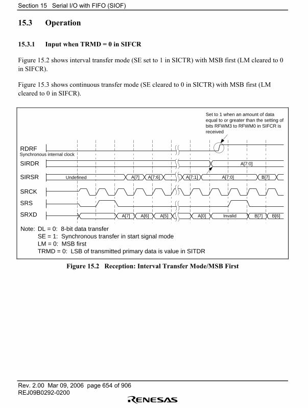
Section 15 Serial I/O with FIFO (SIOF)
Rev. 2.00 Mar 09, 2006 page 654 of 906REJ09B0292-0200
15.3 Operation
15.3.1 Input when TRMD = 0 in SIFCR
Figure 15.2 shows interval transfer mode (SE set to 1 in SICTR) with MSB first (LM cleared to 0in SIFCR).
Figure 15.3 shows continuous transfer mode (SE cleared to 0 in SICTR) with MSB first (LMcleared to 0 in SIFCR).
Note: DL = 0: 8-bit data transferSE = 1: Synchronous transfer in start signal modeLM = 0: MSB firstTRMD = 0: LSB of transmitted primary data is value in SITDR
B[7]A[7] A[7:0]
A[7:0]
A[7:6] A[7:1]
Set to 1 when an amount of data equal to or greater than the setting of bits RFWM3 to RFWM0 in SIFCR is received
A[7] A[6] A[5] A[0] B[7] B[6]InvalidSRXD
SRS
SRCK
SIRSR
SIRDR
RDRFSynchronous internal clock
Undefined
Figure 15.2 Reception: Interval Transfer Mode/MSB First
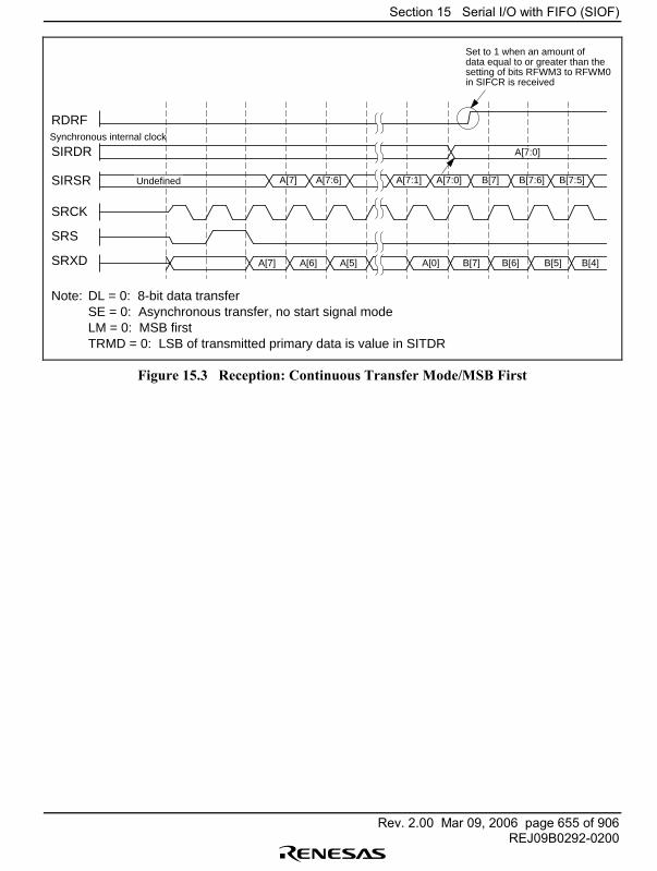
Section 15 Serial I/O with FIFO (SIOF)
Rev. 2.00 Mar 09, 2006 page 655 of 906REJ09B0292-0200
A[7] A[6] A[5] A[0] B[7] B[6] B[5] B[4]
B[7]A[7] A[7:0]
A[7:0]
B[7:6] B[7:5]A[7:6] A[7:1]Undefined
SRXD
SRS
SRCK
SIRSR
SIRDR
RDRF
Note: DL = 0: 8-bit data transferSE = 0: Asynchronous transfer, no start signal modeLM = 0: MSB firstTRMD = 0: LSB of transmitted primary data is value in SITDR
Set to 1 when an amount of data equal to or greater than the setting of bits RFWM3 to RFWM0 in SIFCR is received
Synchronous internal clock
Figure 15.3 Reception: Continuous Transfer Mode/MSB First
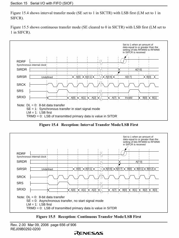
Section 15 Serial I/O with FIFO (SIOF)
Rev. 2.00 Mar 09, 2006 page 656 of 906REJ09B0292-0200
Figure 15.4 shows interval transfer mode (SE set to 1 in SICTR) with LSB first (LM set to 1 inSIFCR).
Figure 15.5 shows continuous transfer mode (SE cleared to 0 in SICTR) with LSB first (LM set to1 in SIFCR).
B[0]A[0] A[0:7]
A[7:0]
A[0:1] A[0:6]
A[0] A[1] A[2] A[7] B[0] B[1]InvalidSRXD
SRS
SRCK
SIRSR
SIRDR
RDRF
Note: DL = 0: 8-bit data transferSE = 1: Synchronous transfer in start signal modeLM = 1: LSB firstTRMD = 0: LSB of transmitted primary data is value in SITDR
Set to 1 when an amount of data equal to or greater than the setting of bits RFWM3 to RFWM0 in SIFCR is received
Synchronous internal clock
Undefined
Figure 15.4 Reception: Interval Transfer Mode/LSB First
SRXD
SRS
SRCK
SIRSR
SIRDR
RDRF
A[0] A[1] A[2] A[7] B[0] B[1] B[2] B[3]
B[0]A[0] A[0:7]
A[7:0]
B[0:1] B[0:2]A[0:1] A[0:6]
Note: DL = 0: 8-bit data transferSE = 0: Asynchronous transfer, no start signal modeLM = 1: LSB firstTRMD = 0: LSB of transmitted primary data is value in SITDR
Set to 1 when an amount of data equal to or greater than the setting of bits RFWM3 to RFWM0 in SIFCR is received
Synchronous internal clock
Undefined
Figure 15.5 Reception: Continuous Transfer Mode/LSB First
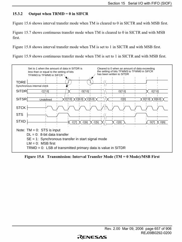
Section 15 Serial I/O with FIFO (SIOF)
Rev. 2.00 Mar 09, 2006 page 657 of 906REJ09B0292-0200
15.3.2 Output when TRMD = 0 in SIFCR
Figure 15.6 shows interval transfer mode when TM is cleared to 0 in SICTR and with MSB first.
Figure 15.7 shows continuous transfer mode when TM is cleared to 0 in SICTR and with MSBfirst.
Figure 15.8 shows interval transfer mode when TM is set to 1 in SICTR and with MSB first.
Figure 15.9 shows continuous transfer mode when TM is set to 1 in SICTR and with MSB first.
STXD
STS
STCK
SITSR
SITDR
TDRE
C[7:0] C[6:0] C[5:0] C[0]
C[7:0] D[7:0] D[7:0] E[7:0]
Set to 1 when the amount of data in SITDR is less than or equal to the setting of bits TFWM3 to TFWM0 in SIFCR
C[7] C[6] C[5] C[0] D[7] D[6]
D[7:0] D[6:0]
Note: TM = 0: STS is inputDL = 0: 8-bit data transferSE = 1: Synchronous transfer in start signal modeLM = 0: MSB firstTRMD = 0: LSB of transmitted primary data is value in SITDR
Cleared to 0 when an amount of data exceeding the setting of bits TFWM3 to TFWM0 in SIFCR has been written to SITDR
Synchronous internal clock
Undefined
Figure 15.6 Transmission: Interval Transfer Mode (TM = 0 Mode)/MSB First

Section 15 Serial I/O with FIFO (SIOF)
Rev. 2.00 Mar 09, 2006 page 658 of 906REJ09B0292-0200
STXD
STS
STCK
SITSR
SITDR
TDRE
C[7:0] C[6:0] C[5:0]
C[7:0] D[7:0] D[7:0] E[7:0]
C[0] D[7:0] D[6:0]
C[7] C[6] C[5] D[7] D[6]C[0] D[5] D[4]
D[5:0] D[4:0]
Set to 1 when the amount of data in SITDR is less than or equal to the setting of bits TFWM3 to TFWM0 in SIFCR
Note: TM = 0: STS is inputDL = 0: 8-bit data transferSE = 0: Asynchronous transfer, no start signal modeLM = 0: MSB firstTRMD = 0: LSB of transmitted primary data is value in SITDR
Cleared to 0 when an amount of data exceeding the setting of bits TFWM3 to TFWM0 in SIFCR has been written to SITDR
Synchronous internal clock
Undefined
Figure 15.7 Transmission: Continuous Transfer Mode (TM = 0 Mode)/MSB First
STXD
STS
STCK
SITSR
SITDR
C[7:0] C[6:0] C[5:0]
C[7:0] D[7:0] D[7:0] E[7:0]
C[1:0] C[0] D[7:0]
C[7] C[6] C[5] C[0] D[7]C[1] D[6] D[5]
D[6:0] D[5:0]
SITDR
TDRE
Set to 1 when the amount of data in SITDR is less than or equal to the setting of bits TFWM3 to TFWM0 in SIFCR
Note: TM = 1: STS is outputDL = 0: 8-bit data transferSE = 1: Synchronous transfer in start signal modeLM = 0: MSB firstTRMD = 0: LSB of transmitted primary data is value in SITDR
Cleared to 0 when an amount of data exceeding the setting of bits TFWM3 to TFWM0 in SIFCR has been written to SITDR
Synchronous internal clock
Undefined
Figure 15.8 Transmission: Interval Transfer Mode (TM = 1 Mode)/MSB First
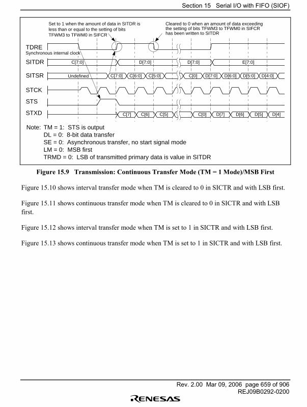
Section 15 Serial I/O with FIFO (SIOF)
Rev. 2.00 Mar 09, 2006 page 659 of 906REJ09B0292-0200
STXD
STS
STCK
SITSR
SITDR
TDRE
C[7:0] C[6:0] C[5:0]
C[7:0] D[7:0] D[7:0] E[7:0]
C[0] D[7:0] D[6:0]
C[7] C[6] C[5] D[7] D[6]C[0] D[5] D[4]
D[5:0] D[4:0]
Set to 1 when the amount of data in SITDR is less than or equal to the setting of bits TFWM3 to TFWM0 in SIFCR
Note: TM = 1: STS is outputDL = 0: 8-bit data transferSE = 0: Asynchronous transfer, no start signal modeLM = 0: MSB firstTRMD = 0: LSB of transmitted primary data is value in SITDR
Cleared to 0 when an amount of data exceeding the setting of bits TFWM3 to TFWM0 in SIFCR has been written to SITDR
Synchronous internal clock
Undefined
Figure 15.9 Transmission: Continuous Transfer Mode (TM = 1 Mode)/MSB First
Figure 15.10 shows interval transfer mode when TM is cleared to 0 in SICTR and with LSB first.
Figure 15.11 shows continuous transfer mode when TM is cleared to 0 in SICTR and with LSBfirst.
Figure 15.12 shows interval transfer mode when TM is set to 1 in SICTR and with LSB first.
Figure 15.13 shows continuous transfer mode when TM is set to 1 in SICTR and with LSB first.
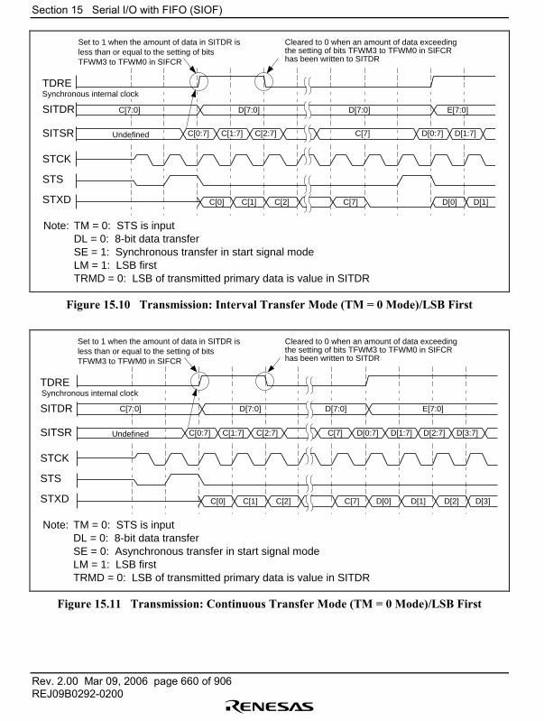
Section 15 Serial I/O with FIFO (SIOF)
Rev. 2.00 Mar 09, 2006 page 660 of 906REJ09B0292-0200
STXD
STS
STCK
SITSR
SITDR
TDRE
C[0:7] C[1:7] C[2:7] C[7]
C[7:0] D[7:0] D[7:0] E[7:0]
C[0] C[1] C[2] C[7] D[0] D[1]
D[0:7] D[1:7]
Set to 1 when the amount of data in SITDR is less than or equal to the setting of bits TFWM3 to TFWM0 in SIFCR
Note: TM = 0: STS is inputDL = 0: 8-bit data transferSE = 1: Synchronous transfer in start signal modeLM = 1: LSB firstTRMD = 0: LSB of transmitted primary data is value in SITDR
Cleared to 0 when an amount of data exceeding the setting of bits TFWM3 to TFWM0 in SIFCR has been written to SITDR
Synchronous internal clock
Undefined
Figure 15.10 Transmission: Interval Transfer Mode (TM = 0 Mode)/LSB First
STXD
STS
STCK
SITSR
SITDR
TDRE
C[0:7] C[1:7] C[2:7]
C[7:0] D[7:0] D[7:0] E[7:0]
C[7] D[0:7] D[1:7]
C[0] C[1] C[2] D[0] D[1]C[7] D[2] D[3]
D[2:7] D[3:7]
Set to 1 when the amount of data in SITDR is less than or equal to the setting of bits TFWM3 to TFWM0 in SIFCR
Note: TM = 0: STS is inputDL = 0: 8-bit data transferSE = 0: Asynchronous transfer in start signal modeLM = 1: LSB firstTRMD = 0: LSB of transmitted primary data is value in SITDR
Cleared to 0 when an amount of data exceeding the setting of bits TFWM3 to TFWM0 in SIFCR has been written to SITDR
Synchronous internal clock
Undefined
Figure 15.11 Transmission: Continuous Transfer Mode (TM = 0 Mode)/LSB First
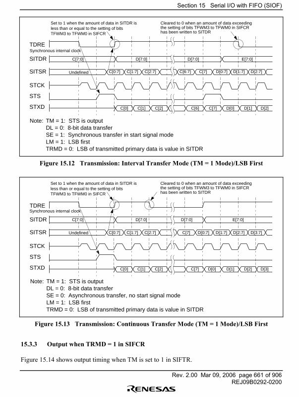
Section 15 Serial I/O with FIFO (SIOF)
Rev. 2.00 Mar 09, 2006 page 661 of 906REJ09B0292-0200
STXD
STS
STCK
SITSR
SITDR
C[0:7] C[1:7] C[2:7]
C[7:0] D[7:0] D[7:0] E[7:0]
C[6:7] C[7] D[0:7]
C[0] C[1] C[2] C[7] D[0]C[6] D[1] D[2]
D[1:7] D[2:7]
TDRE
Set to 1 when the amount of data in SITDR is less than or equal to the setting of bits TFWM3 to TFWM0 in SIFCR
Note: TM = 1: STS is outputDL = 0: 8-bit data transferSE = 1: Synchronous transfer in start signal modeLM = 1: LSB firstTRMD = 0: LSB of transmitted primary data is value in SITDR
Cleared to 0 when an amount of data exceeding the setting of bits TFWM3 to TFWM0 in SIFCR has been written to SITDR
Synchronous internal clock
Undefined
Figure 15.12 Transmission: Interval Transfer Mode (TM = 1 Mode)/LSB First
STXD
STS
STCK
SITSR
SITDR
TDRE
C[0:7] C[1:7] C[2:7]
C[7:0] D[7:0] D[7:0] E[7:0]
C[7] D[0:7] D[1:7]
C[0] C[1] C[2] D[0] D[1]C[7] D[2] D[3]
D[2:7] D[3:7]
Set to 1 when the amount of data in SITDR is less than or equal to the setting of bits TFWM3 to TFWM0 in SIFCR
Note: TM = 1: STS is outputDL = 0: 8-bit data transferSE = 0: Asynchronous transfer, no start signal modeLM = 1: LSB firstTRMD = 0: LSB of transmitted primary data is value in SITDR
Cleared to 0 when an amount of data exceeding the setting of bits TFWM3 to TFWM0 in SIFCR has been written to SITDR
Synchronous internal clock
Undefined
Figure 15.13 Transmission: Continuous Transfer Mode (TM = 1 Mode)/LSB First
15.3.3 Output when TRMD = 1 in SIFCR
Figure 15.14 shows output timing when TM is set to 1 in SIFTR.

Section 15 Serial I/O with FIFO (SIOF)
Rev. 2.00 Mar 09, 2006 page 662 of 906REJ09B0292-0200
B[7
]A
[7]
A[7
:0]
A[7
:0]
A[7
:1]
Set
to 1
whe
n an
am
ount
of d
ata
equa
l to
or g
reat
er th
an
the
setti
ng o
f bits
RF
WM
3 to
RF
WM
0 in
SIF
CR
is r
ecei
ved
A[7
]A
[6]
A[0
]B
[7]
B[6
]In
valid
B[0
]C
[7]
C[6
]C
[0]
SR
XD
SR
S
SR
CK
SIR
SR
SIR
DR
RD
RF
SIR
CD
R
Und
efin
edB
[7:1
]C
[7:0
]
C[7
:0]
C[7
:1]
C[7
]
Inva
lid
B[7
:0]
E[7
:0]
D[7
:0]
D[6
:0]
D[0
]
D[7
:0]
E[7
:0]
E[7
:0]
F[7
:0]
F[7
:0]
F[7
:0]
D[7
]D
[6]
D[0
]E
[7]
E[6
]E
[0]
Z[7
]Z
[6]
Z[0
]S
TX
D
ST
S
ST
CK
SIT
SR
SIT
DR
TD
RE
SIT
CD
R
Und
efin
edE
[6:0
]
Z[7
:0]
Z[7
:0]
Z[7
:0]
Z[7
:0]
Z[6
:0]
Z[7
:0]
E[0
]F
[7:0
]Z
[0]
Not
e:
TM
= 0
: S
TS
is in
put
DL
= 0
: 8-
bit d
ata
tran
sfer
SE
= 1
: S
ynch
rono
us tr
ansf
er in
sta
rt s
igna
l mod
eLM
= 0
: M
SB
firs
tT
RM
D =
1:
LSB
of t
rans
mitt
ed p
rimar
y da
ta is
0
Set
to 1
whe
n th
e am
ount
of d
ata
in S
ITD
R is
less
than
or
equa
l to
the
setti
ng o
f bits
TF
WM
3 to
TF
WM
0 in
SIF
CR
Inva
lid
B[7
:0]
B[7
:0]
Syn
chro
nous
inte
rnal
clo
ck
Syn
chro
nous
inte
rnal
clo
ck
Figure 15.14 Transmission: TRMD = 1 Mode
Section 15 Serial I/O with FIFO (SIOF)
Rev. 2.00 Mar 09, 2006 page 663 of 906REJ09B0292-0200
15.4 SIOF Interrupt Sources and DMAC
Each SIOF channel has four interrupt sources: the receive-overrun-error interrupt (RERI0) request,transmit-underrun-error interrupt (TERI0) request, receive-data-full interrupt/receive-control-data-register-full interrupt (RDFI0) request, and transmit-data-empty interrupt/transmit-control-data-register-empty interrupt (TDEI0) request. Table 15.3 shows the interrupt sources and their relativepriorities. The RDFI0 and TDEI0 interrupts are enabled by the RIE, RCIE, TIE, and TCIE bits,respectively, in SICTR. The RERI0 and TERI0 interrupts cannot be disabled.
An RDFI0 interrupt request is generated when the RDRF bit is set to 1 or the RCD bit is set to 1 inSISTR.
The DMACE bit should be cleared to 0 in SICTR to have interrupts triggered by both the RDRFbit and the RCD bit processed by the CPU. In this case the CPU should process interrupts afterreading SISTR and determining which bit triggered them.
Set the DMACE bit to 1 in SICTR to have interrupts triggered by the RDRF bit processed by theDMAC and interrupts triggered by the RCD bit processed by the CPU. In addition, the priority ofinterrupts from SIOF should be set to a high level in order to activate the interrupt controller(INTC). This will cause interrupts triggered by the RDRF bit to be sent to the DMAC andinterrupts triggered by the RCD bit to be sent to the INTC. The data in SIRDR is read and if theamount of primary data is less than the setting of bits RFWM3 to RFWM0 in SIFCR, RDRF isautomatically cleared to 0. Interrupts triggered by the RCD bit cannot be processed by the DMAC.
An TDEI0 interrupt request is generated when the TDRE bit is set to 1 or the TCD bit is set to 1 inSISTR.
The DMACE bit should be cleared to 0 in SICTR to have interrupts triggered by both the TDREbit and the TCD bit processed by the CPU. In this case the CPU should process interrupts afterreading SISTR and determining which bit triggered them.
Set the DMACE bit to 1 in SICTR to have interrupts triggered by the TDRE bit processed by theDMAC and interrupts triggered by the TCD bit processed by the CPU. In addition, the priority ofinterrupts from SIOF should be set to a high level in order to activate the INTC. This will causeinterrupts triggered by the TDRE bit to be sent to the DMAC and interrupts triggered by the TCDbit to be sent to the INTC. The DMAC writes data to SIRDR and if the amount of primary data isequal to or greater than the setting of bits TFWM3 to TFWM0 in SIFCR, TDRE is automaticallycleared to 0. Interrupts triggered by the TCD bit cannot be processed by the DMAC.
When the RERR bit is set to 1 in SISTR, an RERI0 interrupt request is generated.
When the TERR bit is set to 1 in SISTR, a TERI0 interrupt request is generated.

Section 15 Serial I/O with FIFO (SIOF)
Rev. 2.00 Mar 09, 2006 page 664 of 906REJ09B0292-0200
Channel interrupt priority levels are set by means of the IRPE register, as described in section 5,Interrupt Controller (INTC).
Table 15.3 SIOF Interrupt Sources
Interrupt Source Description DMAC Activation Priority
RERI0 Receive overrun error (RERR) Not possible High
TERI0 Transmit underrun error (TERR) Not possible ↑
RDFI0 Receive data register full (RDRF)/Receive Control Data Register Full (RCD)
Possible* ↓
TDEI0 Transmit data register empty (TDRE)/Transmit Control Data Register Empty (TCD)
Possible* Low
Note: * The interrupt sources that can activate the DMAC are receive data full (RDRF) and transmitdata empty (TDRE).It is not possible for receive control data full (RCD) or transmit control data empty (TCD) toactivate the DMAC.
The DMAC should be used to process RDRF and TDRE interrupts when using SIRCDR andSITCDR, and the DMACE bit must be set to 1 in SICTR when using the CPU to process RCDand TCD interrupts.The DMACE bit should be cleared to 0 in SICTR if neither SIRCDR nor SITCDR is used andboth RDRF and TDRE interrupts as well as RCD and TCD interrupts are to be processed bythe CPU.
Section 16 Serial I/O (SIO)
Rev. 2.00 Mar 09, 2006 page 665 of 906REJ09B0292-0200
Section 16 Serial I/O (SIO)
16.1 Overview
A two-channel simple synchronous serial I/O is provided on-chip. The serial I/O functions mainlyas an interface between the chip and a codec or modem analog front-end.
16.1.1 Features
The serial I/O has the following features:
• Full-duplex operationIndependent transmit/receive registers and independent transmit/receive clocks
• Double-buffered transmit/receive portsContinuous data transmission/reception possible
• Interval transfer mode and continuous transfer mode• Memory-mapped receive register, transmit register, control register, and status register
With the exception of SIRSR and SITSR, these registers are memory-mapped and can beaccessed by a MOV instruction.
• Choice of 8- or 16-bit data length• Data transfer communication by means of polling or interrupts
Data transfer can be monitored by polling the receive data register full flag (RDRF) andtransmit data register empty flag (TDRE) in the serial status register. Interrupt requests can begenerated during data transfer by setting the receive interrupt request flag and transmitinterrupt request flag.
• MSB-first transfer between SIO and data I/O
Figure 16.1 shows a block diagram of the serial I/O.
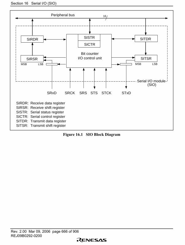
Section 16 Serial I/O (SIO)
Rev. 2.00 Mar 09, 2006 page 666 of 906REJ09B0292-0200
Peripheral bus 16
SIRDR SITDRSISTR
SICTR
STCKSRCKSRxD
SIRDR: Receive data registerSIRSR: Receive shift registerSISTR: Serial status registerSICTR: Serial control registerSITDR: Transmit data registerSITSR: Transmit shift register
Bit counterI/O control unitSIRSR SITSR
STxDSRS STS
MSB LSB MSB LSB
Serial I/O module (SIO)
Figure 16.1 SIO Block Diagram
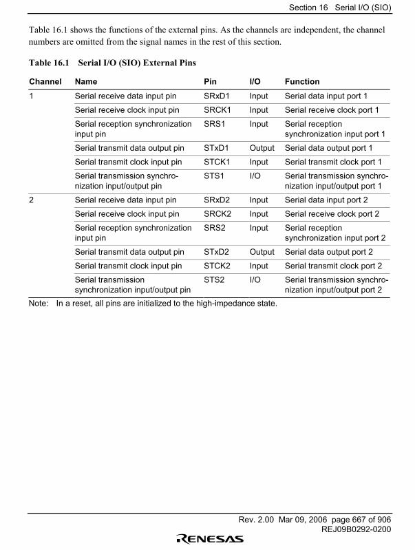
Section 16 Serial I/O (SIO)
Rev. 2.00 Mar 09, 2006 page 667 of 906REJ09B0292-0200
Table 16.1 shows the functions of the external pins. As the channels are independent, the channelnumbers are omitted from the signal names in the rest of this section.
Table 16.1 Serial I/O (SIO) External Pins
Channel Name Pin I/O Function
1 Serial receive data input pin SRxD1 Input Serial data input port 1
Serial receive clock input pin SRCK1 Input Serial receive clock port 1
Serial reception synchronizationinput pin
SRS1 Input Serial receptionsynchronization input port 1
Serial transmit data output pin STxD1 Output Serial data output port 1
Serial transmit clock input pin STCK1 Input Serial transmit clock port 1
Serial transmission synchro-nization input/output pin
STS1 I/O Serial transmission synchro-nization input/output port 1
2 Serial receive data input pin SRxD2 Input Serial data input port 2
Serial receive clock input pin SRCK2 Input Serial receive clock port 2
Serial reception synchronizationinput pin
SRS2 Input Serial receptionsynchronization input port 2
Serial transmit data output pin STxD2 Output Serial data output port 2
Serial transmit clock input pin STCK2 Input Serial transmit clock port 2
Serial transmissionsynchronization input/output pin
STS2 I/O Serial transmission synchro-nization input/output port 2
Note: In a reset, all pins are initialized to the high-impedance state.
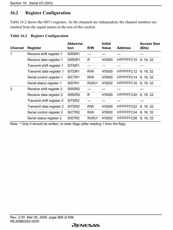
Section 16 Serial I/O (SIO)
Rev. 2.00 Mar 09, 2006 page 668 of 906REJ09B0292-0200
16.2 Register Configuration
Table 16.2 shows the SIO�s registers. As the channels are independent, the channel numbers areomitted from the signal names in the rest of this section.
Table 16.2 Register Configuration
Channel RegisterAbbrevia-tion R/W
InitialValue Address
Access Size(Bits)
1 Receive shift register 1 SIRSR1 � � � �
Receive data register 1 SIRDR1 R H'0000 H'FFFFFC10 8, 16, 32
Transmit shift register 1 SITSR1 � � � �
Transmit data register 1 SITDR1 R/W H'0000 H'FFFFFC12 8, 16, 32
Serial control register 1 SICTR1 R/W H'0000 H'FFFFFC14 8, 16, 32
Serial status register 1 SISTR1 R/(W)* H'0002 H'FFFFFC16 8, 16, 32
2 Receive shift register 2 SIRSR2 � � � �
Receive data register 2 SIRDR2 R H'0000 H'FFFFFC20 8, 16, 32
Transmit shift register 2 SITSR2 � � � �
Transmit data register 2 SITDR2 R/W H'0000 H'FFFFFC22 8, 16, 32
Serial control register 2 SICTR2 R/W H'0000 H'FFFFFC24 8, 16, 32
Serial status register 2 SISTR2 R/(W)* H'0002 H'FFFFFC26 8, 16, 32Note: * Only 0 should be written, to clear flags (after reading 1 from the flag).
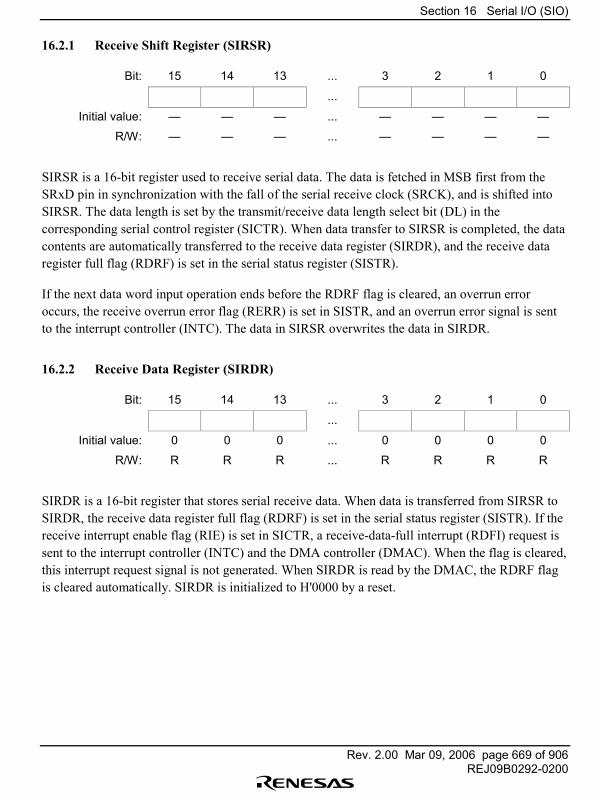
Section 16 Serial I/O (SIO)
Rev. 2.00 Mar 09, 2006 page 669 of 906REJ09B0292-0200
16.2.1 Receive Shift Register (SIRSR)
Bit: 15 14 13 ... 3 2 1 0
...
Initial value: � � � ... � � � �
R/W: � � � ... � � � �
SIRSR is a 16-bit register used to receive serial data. The data is fetched in MSB first from theSRxD pin in synchronization with the fall of the serial receive clock (SRCK), and is shifted intoSIRSR. The data length is set by the transmit/receive data length select bit (DL) in thecorresponding serial control register (SICTR). When data transfer to SIRSR is completed, the datacontents are automatically transferred to the receive data register (SIRDR), and the receive dataregister full flag (RDRF) is set in the serial status register (SISTR).
If the next data word input operation ends before the RDRF flag is cleared, an overrun erroroccurs, the receive overrun error flag (RERR) is set in SISTR, and an overrun error signal is sentto the interrupt controller (INTC). The data in SIRSR overwrites the data in SIRDR.
16.2.2 Receive Data Register (SIRDR)
Bit: 15 14 13 ... 3 2 1 0
...
Initial value: 0 0 0 ... 0 0 0 0
R/W: R R R ... R R R R
SIRDR is a 16-bit register that stores serial receive data. When data is transferred from SIRSR toSIRDR, the receive data register full flag (RDRF) is set in the serial status register (SISTR). If thereceive interrupt enable flag (RIE) is set in SICTR, a receive-data-full interrupt (RDFI) request issent to the interrupt controller (INTC) and the DMA controller (DMAC). When the flag is cleared,this interrupt request signal is not generated. When SIRDR is read by the DMAC, the RDRF flagis cleared automatically. SIRDR is initialized to H'0000 by a reset.

Section 16 Serial I/O (SIO)
Rev. 2.00 Mar 09, 2006 page 670 of 906REJ09B0292-0200
16.2.3 Transmit Shift Register (SITSR)
Bit: 15 14 13 ... 3 2 1 0
...
Initial value: � � � ... � � � �
R/W: � � � ... � � � �
SITSR is a 16-bit register used to transmit serial data. The contents of this register are shifted inMSB-first order in synchronization with the rising edge of the serial transmit clock (STCK), andoutput from the STxD pin. The transfer data length is set by the transmit/receive data length selectbit (DL) in the serial control register (SICTR). When the DL bit is cleared to 0 (8-bit data length),the lower 8 bits of SITDR are output. When the serial transmission synchronization signal (STS)goes high, or the last data transmission ends without the synchronization enable (SE) bit being setin SICTR, the contents of the transmit data register (SITDR) are transferred to SITSR, and ifTDRE is 0, TDRE is then set. If output of the next data begins before TDRE is cleared, an overrunerror occurs, the transmit overrun error flag (TERR) is set in SISTR, and a transmit overrun errorinterrupt request is sent to the INTC.
16.2.4 Transmit Data Register (SITDR)
Bit: 15 14 13 ... 3 2 1 0
...
Initial value: 0 0 0 ... 0 0 0 0
R/W: R/W R/W R/W ... R/W R/W R/W R/W
SITDR is a 16-bit register that stores serial transmit data. Data should be written to SITDR whenthe transmit data register empty flag (TDRE) is set to 1 in SISTR. If data is written to SITDRwhen TDRE is 0, the previous data will be overwritten. When STS goes high or data output fromtransmit shift register SITSR ends with the SE bit cleared to 0 in SICTR, the data in SITDR isautomatically transferred to SITSR, and if TDRE is 0, TDRE is then set. If the transmit interruptenable flag (TIE) is set, a transmit-data-empty interrupt (TDEI) request is sent to the INTC andDMAC. When TIE is cleared, this interrupt request is not generated. When the DMAC writes toSITDR, the TDRE flag is cleared automatically. The TDRE flag is set only by hardware. SITDR isinitialized to H'0000 by a reset.

Section 16 Serial I/O (SIO)
Rev. 2.00 Mar 09, 2006 page 671 of 906REJ09B0292-0200
16.2.5 Serial Control Register (SICTR)
Bit: 15 14 13 12 11 10 9 8� � � � � � � �
Initial value: 0 0 0 0 0 0 0 0R/W: R R R R R R R R
Bit: 7 6 5 4 3 2 1 0� TM SE DL TIE RIE TE RE
Initial value: 0 0 0 0 0 0 0 0R/W: R R/W R/W R/W R/W R/W R/W R/W
SICTR is a 16-bit register used to set parameters for serial port control. SICTR is initialized toH'0000 by a reset.
When modifying bit 4, 5, or 6 (TM, SE, or DL), TE and RE should be cleared to 0 beforehand.
Bits 15 to 7�Reserved: These bits are always read as 0. The write value should always be 0.
Bit 6�Transfer Mode Control (TM): Specifies whether the transmission synchronization signal isto be input from an external source or generated internally by the chip. When this flag is cleared,the transmission synchronization signal is STS pin input. When this flag is set, the transmissionsynchronization signal is generated by the chip, and is output to an external device from the STSpin. This bit does not affect reception.
Bit 6: TM Description0 External signal input from STS pin is used as transmission start indication
(Initial value)1 Internal signal output from STS pin is used as transmission start indication
Bit 5�Synchronization Signal Enable (SE): Specifies whether the synchronization signals are tobe used for all serial data transfers, or only for the first transfer.
When this bit is cleared to 0, the synchronization signals (SRS and STS) are necessary only for thefirst data transfer, and are not required for subsequent transfers. When this bit is set to 1, thesynchronization signals are necessary for all data transfers.
Bit 5: SE Description0 Continuous mode: SRS and STS are used only for the first data transfer
(Initial value)1 Interval mode: SRS and STS are used for all data transfers
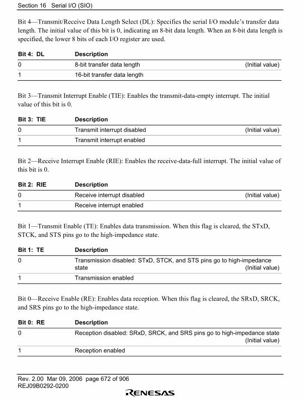
Section 16 Serial I/O (SIO)
Rev. 2.00 Mar 09, 2006 page 672 of 906REJ09B0292-0200
Bit 4�Transmit/Receive Data Length Select (DL): Specifies the serial I/O module�s transfer datalength. The initial value of this bit is 0, indicating an 8-bit data length. When an 8-bit data length isspecified, the lower 8 bits of each I/O register are used.
Bit 4: DL Description
0 8-bit transfer data length (Initial value)
1 16-bit transfer data length
Bit 3�Transmit Interrupt Enable (TIE): Enables the transmit-data-empty interrupt. The initialvalue of this bit is 0.
Bit 3: TIE Description
0 Transmit interrupt disabled (Initial value)
1 Transmit interrupt enabled
Bit 2�Receive Interrupt Enable (RIE): Enables the receive-data-full interrupt. The initial value ofthis bit is 0.
Bit 2: RIE Description
0 Receive interrupt disabled (Initial value)
1 Receive interrupt enabled
Bit 1�Transmit Enable (TE): Enables data transmission. When this flag is cleared, the STxD,STCK, and STS pins go to the high-impedance state.
Bit 1: TE Description
0 Transmission disabled: STxD, STCK, and STS pins go to high-impedancestate (Initial value)
1 Transmission enabled
Bit 0�Receive Enable (RE): Enables data reception. When this flag is cleared, the SRxD, SRCK,and SRS pins go to the high-impedance state.
Bit 0: RE Description
0 Reception disabled: SRxD, SRCK, and SRS pins go to high-impedance state(Initial value)
1 Reception enabled
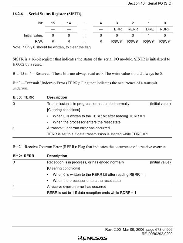
Section 16 Serial I/O (SIO)
Rev. 2.00 Mar 09, 2006 page 673 of 906REJ09B0292-0200
16.2.6 Serial Status Register (SISTR)
Bit: 15 14 ... 4 3 2 1 0
� � ... � TERR RERR TDRE RDRF
Initial value: 0 0 ... 0 0 0 1 0
R/W: R R ... R R/(W)* R/(W)* R/(W)* R/(W)*Note: * Only 0 should be written, to clear the flag.
SISTR is a 16-bit register that indicates the status of the serial I/O module. SISTR is initialized toH'0002 by a reset.
Bits 15 to 4�Reserved: These bits are always read as 0. The write value should always be 0.
Bit 3�Transmit Underrun Error (TERR): Flag that indicates the occurrence of a transmitunderrun.
Bit 3: TERR Description
0 Transmission is in progress, or has ended normally (Initial value)
[Clearing conditions]
• When 0 is written to the TERR bit after reading TERR = 1
• When the processor enters the reset state1 A transmit underrun error has occurred
TERR is set to 1 if data transmission is started while TDRE = 1
Bit 2�Receive Overrun Error (RERR): Flag that indicates the occurrence of a receive overrun.
Bit 2: RERR Description
0 Reception is in progress, or has ended normally (Initial value)
[Clearing conditions]
• When 0 is written to the RERR bit after reading RERR = 1
• When the processor enters the reset state1 A receive overrun error has occurred
RERR is set to 1 if data reception ends while RDRF = 1
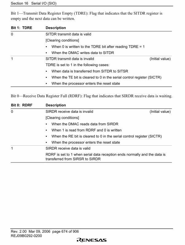
Section 16 Serial I/O (SIO)
Rev. 2.00 Mar 09, 2006 page 674 of 906REJ09B0292-0200
Bit 1�Transmit Data Register Empty (TDRE): Flag that indicates that the SITDR register isempty and the next data can be written.
Bit 1: TDRE Description
0 SITDR transmit data is valid
[Clearing conditions]
• When 0 is written to the TDRE bit after reading TDRE = 1
• When the DMAC writes data to SITDR1 SITDR transmit data is invalid (Initial value)
TDRE is set to 1 in the following cases:
• When data is transferred from SITDR to SITSR
• When the TE bit is cleared to 0 in the serial control register (SICTR)
• When the processor enters the reset state
Bit 0�Receive Data Register Full (RDRF): Flag that indicates that SIRDR receive data is waiting.
Bit 0: RDRF Description
0 SIRDR receive data is invalid (Initial value)
[Clearing conditions]
• When the DMAC reads data from SIRDR
• When 1 is read from RDRF and 0 is written
• When the RE bit is cleared to 0 in the serial control register (SICTR)
• When the processor enters the reset state1 SIRDR receive data is valid
RDRF is set to 1 when serial data reception ends normally and the data istransferred from SIRSR to SIRDR
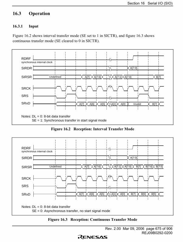
Section 16 Serial I/O (SIO)
Rev. 2.00 Mar 09, 2006 page 675 of 906REJ09B0292-0200
16.3 Operation
16.3.1 Input
Figure 16.2 shows interval transfer mode (SE set to 1 in SICTR), and figure 16.3 showscontinuous transfer mode (SE cleared to 0 in SICTR).
B[7]
SRxD
Notes: DL = 0: 8-bit data transfer SE = 1: Synchronous transfer in start signal mode
SRS
SRCK
A[7]SIRSR A[7:0]A[7:6] A[7:1]
A[7:0]SIRDR
RDRF
A[7] A[6] A[5] A[0]A[1] B[7]
synchronous internal clock
Undefined
Invalid
Figure 16.2 Reception: Interval Transfer Mode
SRxD
Notes: DL = 0: 8-bit data transfer SE = 0: Asynchronous transfer, no start signal mode
SRCK
SRS
A[7] A[6] A[5] A[0] B[7] B[6] B[5]A[1]
SIRSR B[7]A[7] A[7:0] B[7:6] B[7:5]A[7:6] A[7:1]
A[7:0]SIRDR
RDRFsynchronous internal clock
Undefined
Figure 16.3 Reception: Continuous Transfer Mode
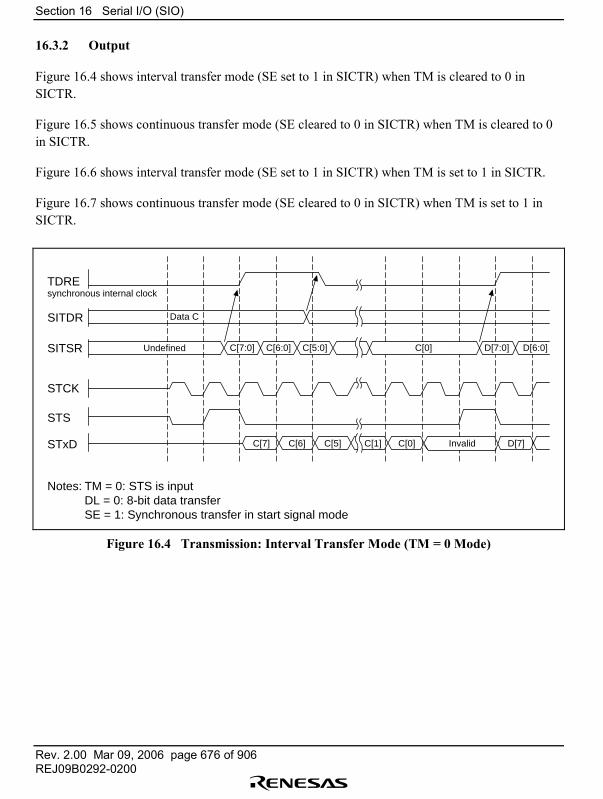
Section 16 Serial I/O (SIO)
Rev. 2.00 Mar 09, 2006 page 676 of 906REJ09B0292-0200
16.3.2 Output
Figure 16.4 shows interval transfer mode (SE set to 1 in SICTR) when TM is cleared to 0 inSICTR.
Figure 16.5 shows continuous transfer mode (SE cleared to 0 in SICTR) when TM is cleared to 0in SICTR.
Figure 16.6 shows interval transfer mode (SE set to 1 in SICTR) when TM is set to 1 in SICTR.
Figure 16.7 shows continuous transfer mode (SE cleared to 0 in SICTR) when TM is set to 1 inSICTR.
STxD
Notes: TM = 0: STS is input DL = 0: 8-bit data transfer SE = 1: Synchronous transfer in start signal mode
STCK
STS
C[7] C[6] C[5] C[0] D[7]C[1]
SITSR C[6:0]C[7:0] D[7:0] D[6:0]C[5:0] C[0]
Data CSITDR
TDREsynchronous internal clock
Undefined
Invalid
Figure 16.4 Transmission: Interval Transfer Mode (TM = 0 Mode)
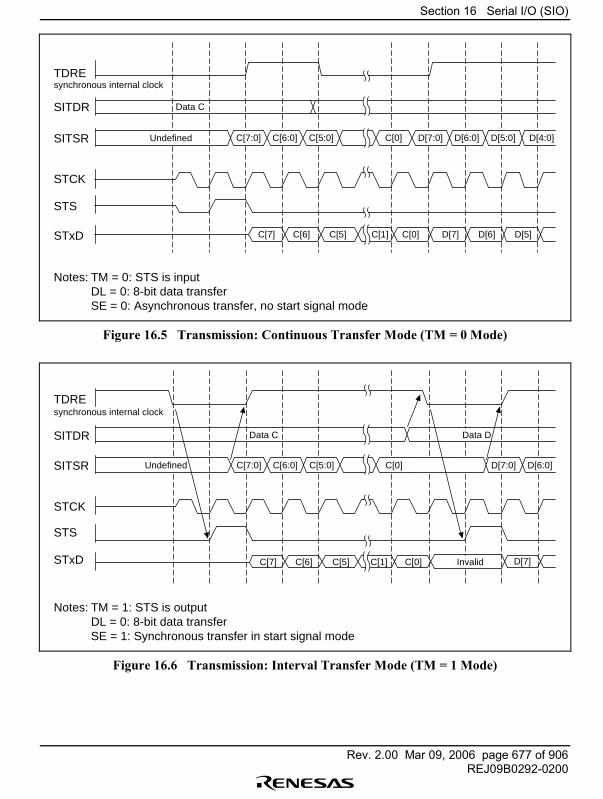
Section 16 Serial I/O (SIO)
Rev. 2.00 Mar 09, 2006 page 677 of 906REJ09B0292-0200
C[6:0]
STxD
Notes: TM = 0: STS is input DL = 0: 8-bit data transfer SE = 0: Asynchronous transfer, no start signal mode
STCK
STS
C[7] C[6] C[5] C[0] D[7] D[6] D[5]C[1]
C[7:0]SITSR D[7:0] D[6:0] D[5:0] D[4:0]C[5:0] C[0]
SITDR
TDREsynchronous internal clock
Undefined
Data C
Figure 16.5 Transmission: Continuous Transfer Mode (TM = 0 Mode)
C[6:0]
STxD
Notes: TM = 1: STS is output DL = 0: 8-bit data transfer SE = 1: Synchronous transfer in start signal mode
STCK
STS
C[7] C[6] C[5] C[0] D[7]C[1]
C[7:0]SITSR D[7:0] D[6:0]C[5:0]
Data CSITDR
TDREsynchronous internal clock
Undefined C[0]
Invalid
Data D
Figure 16.6 Transmission: Interval Transfer Mode (TM = 1 Mode)
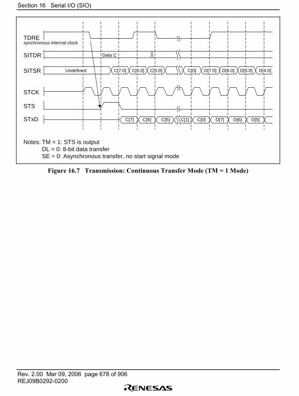
Section 16 Serial I/O (SIO)
Rev. 2.00 Mar 09, 2006 page 678 of 906REJ09B0292-0200
C[6:0]
STxD
Notes: TM = 1: STS is output DL = 0: 8-bit data transfer SE = 0: Asynchronous transfer, no start signal mode
STCK
STS
C[7] C[6] C[5] C[0] D[7] D[6] D[5]C[1]
C[7:0]SITSR D[7:0] D[6:0] D[5:0] D[4:0]C[5:0] C[0]
Data CSITDR
TDREsynchronous internal clock
Undefined
Figure 16.7 Transmission: Continuous Transfer Mode (TM = 1 Mode)
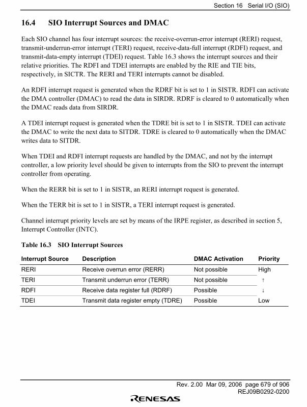
Section 16 Serial I/O (SIO)
Rev. 2.00 Mar 09, 2006 page 679 of 906REJ09B0292-0200
16.4 SIO Interrupt Sources and DMAC
Each SIO channel has four interrupt sources: the receive-overrun-error interrupt (RERI) request,transmit-underrun-error interrupt (TERI) request, receive-data-full interrupt (RDFI) request, andtransmit-data-empty interrupt (TDEI) request. Table 16.3 shows the interrupt sources and theirrelative priorities. The RDFI and TDEI interrupts are enabled by the RIE and TIE bits,respectively, in SICTR. The RERI and TERI interrupts cannot be disabled.
An RDFI interrupt request is generated when the RDRF bit is set to 1 in SISTR. RDFI can activatethe DMA controller (DMAC) to read the data in SIRDR. RDRF is cleared to 0 automatically whenthe DMAC reads data from SIRDR.
A TDEI interrupt request is generated when the TDRE bit is set to 1 in SISTR. TDEI can activatethe DMAC to write the next data to SITDR. TDRE is cleared to 0 automatically when the DMACwrites data to SITDR.
When TDEI and RDFI interrupt requests are handled by the DMAC, and not by the interruptcontroller, a low priority level should be given to interrupts from the SIO to prevent the interruptcontroller from operating.
When the RERR bit is set to 1 in SISTR, an RERI interrupt request is generated.
When the TERR bit is set to 1 in SISTR, a TERI interrupt request is generated.
Channel interrupt priority levels are set by means of the IRPE register, as described in section 5,Interrupt Controller (INTC).
Table 16.3 SIO Interrupt Sources
Interrupt Source Description DMAC Activation Priority
RERI Receive overrun error (RERR) Not possible High
TERI Transmit underrun error (TERR) Not possible ↑
RDFI Receive data register full (RDRF) Possible ↓
TDEI Transmit data register empty (TDRE) Possible Low
Section 16 Serial I/O (SIO)
Rev. 2.00 Mar 09, 2006 page 680 of 906REJ09B0292-0200
Section 17 16-Bit Timer Pulse Unit (TPU)
Rev. 2.00 Mar 09, 2006 page 681 of 906REJ09B0292-0200
Section 17 16-Bit Timer Pulse Unit (TPU)
17.1 Overview
An on-chip 16-bit timer pulse unit (TPU) is provided that comprises three 16-bit timer channels.
17.1.1 Features
The TPU has the following features:
• Maximum 8-pulse input/output• A total of eight timer general registers (TGRs) are provided (four for channel 0 and two each
for channels 1, and 2). Each register can be set independently as an output compare/input capture register. TGRC and TGRD for channel 0 can be used as buffer registers
• Choice of seven or eight counter input clocks for each channel• The following operations can be set for each channel:
Waveform output by compare match: Selection of 0, 1, or toggle output Input capture function: Choice of rising edge, falling edge, or both edge detection Counter clear operation: Counter clearing possible by compare match or input capture Synchronous operation: Multiple timer counters (TCNT) can be written to simultaneously
simultaneous clearing by compare match and input capture possibleregister simultaneous input/output possible by counter synchronous operation
PWM mode: Any PWM output duty can be set maximum of 7-phase PWM output possibleby combination with synchronous operation
• Buffer operation settable for channel 0 Input capture register double-buffering possible Automatic rewriting of output compare register possible
• Phase counting mode settable independently for each of channels 1, and 2 Two-phase encoder pulse up/down-count possible
• Fast access via internal 16-bit bus Fast access is possible via a 16-bit bus interface
• 13 interrupt sources For channel 0 four compare match/input capture dual-function interrupts and one overflow
interrupt can be requested independently
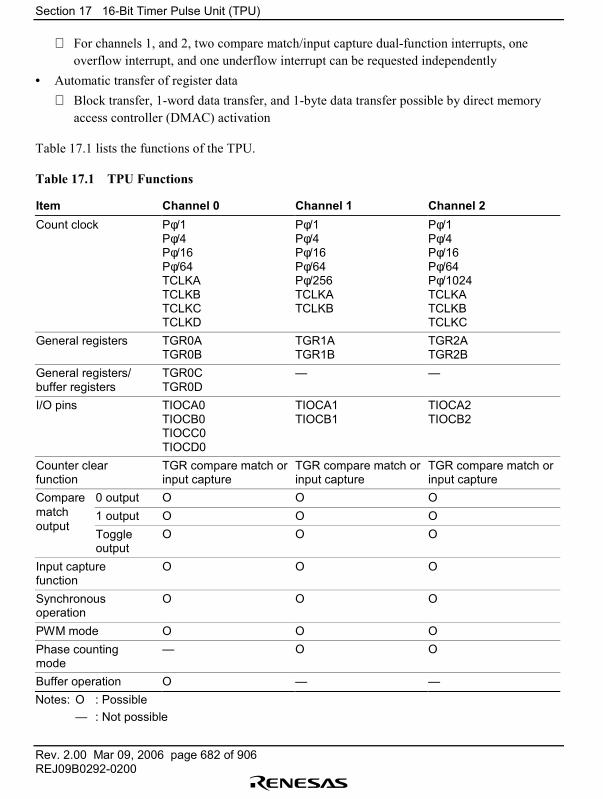
Section 17 16-Bit Timer Pulse Unit (TPU)
Rev. 2.00 Mar 09, 2006 page 682 of 906REJ09B0292-0200
For channels 1, and 2, two compare match/input capture dual-function interrupts, oneoverflow interrupt, and one underflow interrupt can be requested independently
• Automatic transfer of register data Block transfer, 1-word data transfer, and 1-byte data transfer possible by direct memory
access controller (DMAC) activation
Table 17.1 lists the functions of the TPU.
Table 17.1 TPU Functions
Item Channel 0 Channel 1 Channel 2Count clock Pφ/1
Pφ/4Pφ/16Pφ/64TCLKATCLKBTCLKCTCLKD
Pφ/1Pφ/4Pφ/16Pφ/64Pφ/256TCLKATCLKB
Pφ/1Pφ/4Pφ/16Pφ/64Pφ/1024TCLKATCLKBTCLKC
General registers TGR0ATGR0B
TGR1ATGR1B
TGR2ATGR2B
General registers/buffer registers
TGR0CTGR0D
� �
I/O pins TIOCA0TIOCB0TIOCC0TIOCD0
TIOCA1TIOCB1
TIOCA2TIOCB2
Counter clearfunction
TGR compare match orinput capture
TGR compare match orinput capture
TGR compare match orinput capture
Compare 0 output O O Omatch 1 output O O Ooutput
Toggleoutput
O O O
Input capturefunction
O O O
Synchronousoperation
O O O
PWM mode O O OPhase countingmode
� O O
Buffer operation O � �Notes: O : Possible
� : Not possible

Section 17 16-Bit Timer Pulse Unit (TPU)
Rev. 2.00 Mar 09, 2006 page 683 of 906REJ09B0292-0200
Item Channel 0 Channel 1 Channel 2
DMAC activation TGR compare match orinput capture
� �
Interrupt sources 5 sources• Compare match or
input capture 0A• Compare match or
input capture 0B• Compare match or
input capture 0C• Compare match or
input capture 0D• Overflow
4 sources• Compare match or
input capture 1A• Compare match or
input capture 1B• Overflow• Underflow
4 sources• Compare match or
input capture 2A• Compare match or
input capture 2B• Overflow• Underflow
Note: � : Not possible
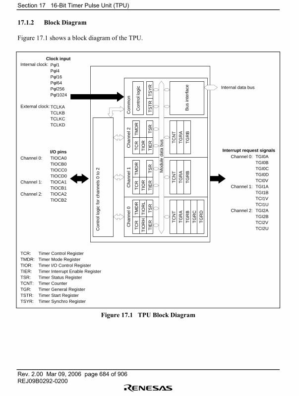
Section 17 16-Bit Timer Pulse Unit (TPU)
Rev. 2.00 Mar 09, 2006 page 684 of 906REJ09B0292-0200
17.1.2 Block Diagram
Figure 17.1 shows a block diagram of the TPU.
Con
trol
logi
cT
MD
R
TS
R
TC
R
TIO
R
TIE
R
TG
RA
TC
NT
TG
RB
TG
RC
Cha
nnel
1
TM
DR
TS
R
TC
R
TIO
R
TIE
R TG
RA
TC
NT
TG
RB
Cha
nnel
0
TM
DR
TS
R
TC
R
TIO
RH
TIE
R
Con
trol
logi
c fo
r ch
anne
ls 0
to 2
TG
RA
TC
NT
TG
RB
TG
RD
TS
YR
TS
TR
Clock inputPφ/1Pφ/4Pφ/16Pφ/64Pφ/256Pφ/1024
TCLKATCLKBTCLKCTCLKD
I/O pinsTIOCA0TIOCB0TIOCC0TIOCD0TIOCA1TIOCB1TIOCA2TIOCB2
Interrupt request signalsChannel 0:
Channel 1:
Channel 2:
Internal data bus
TIO
RL
Mod
ule
data
bus
TGI0ATGI0BTGI0CTGI0DTCI0VTGI1ATGI1BTCI1VTCI1UTGI2ATGI2BTCI2VTCI2U
Internal clock:
External clock:
Channel 0:
Channel 1:
Channel 2:
TCR: Timer Control RegisterTMDR: Timer Mode RegisterTIOR: Timer I/O Control RegisterTIER: Timer Interrupt Enable RegisterTSR: Timer Status RegisterTCNT: Timer CounterTGR: Timer General RegisterTSTR: Timer Start RegisterTSYR: Timer Synchro Register
Cha
nnel
2C
omm
on
Bus
inte
rfac
e
Figure 17.1 TPU Block Diagram

Section 17 16-Bit Timer Pulse Unit (TPU)
Rev. 2.00 Mar 09, 2006 page 685 of 906REJ09B0292-0200
17.1.3 Pin Configuration
Table 17.2 shows the pin configuration of the TPU.
Table 17.2 Pin Configuration
Channel Name Abbreviation I/O Function
All Clock input A TCLKA Input External clock A input pin(Channel 1 phase counting mode Aphase input)
Clock input B TCLKB Input External clock B input pin(Channel 1 phase counting mode Bphase input)
Clock input C TCLKC Input External clock C input pin(Channel 2 phase counting mode Aphase input)
Clock input D TCLKD Input External clock D input pin(Channel 2 phase counting mode Bphase input)
0 Input capture/outputcompare match A0
TIOCA0 I/O TGR0A input capture input/outputcompare output/PWM output pin
Input capture/outputcompare match B0
TIOCB0 I/O TGR0B input capture input/outputcompare output/PWM output pin
Input capture/outputcompare match C0
TIOCC0 I/O TGR0C input capture input/outputcompare output/PWM output pin
Input capture/outputcompare match D0
TIOCD0 I/O TGR0D input capture input/outputcompare output/PWM output pin
1 Input capture/outputcompare match A1
TIOCA1 I/O TGR1A input capture input/outputcompare output/PWM output pin
Input capture/outputcompare match B1
TIOCB1 I/O TGR1B input capture input/outputcompare output/PWM output pin
2 Input capture/outputcompare match A2
TIOCA2 I/O TGR2A input capture input/outputcompare output/PWM output pin
Input capture/outputcompare match B2
TIOCB2 I/O TGR2B input capture input/outputcompare output/PWM output pin
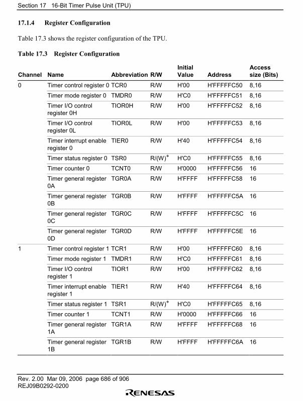
Section 17 16-Bit Timer Pulse Unit (TPU)
Rev. 2.00 Mar 09, 2006 page 686 of 906REJ09B0292-0200
17.1.4 Register Configuration
Table 17.3 shows the register configuration of the TPU.
Table 17.3 Register Configuration
Channel Name Abbreviation R/WInitialValue Address
Accesssize (Bits)
0 Timer control register 0 TCR0 R/W H'00 H'FFFFFC50 8,16
Timer mode register 0 TMDR0 R/W H'C0 H'FFFFFC51 8,16
Timer I/O controlregister 0H
TIOR0H R/W H'00 H'FFFFFC52 8,16
Timer I/O controlregister 0L
TIOR0L R/W H'00 H'FFFFFC53 8,16
Timer interrupt enableregister 0
TIER0 R/W H'40 H'FFFFFC54 8,16
Timer status register 0 TSR0 R/(W)* H'C0 H'FFFFFC55 8,16
Timer counter 0 TCNT0 R/W H'0000 H'FFFFFC56 16
Timer general register0A
TGR0A R/W H'FFFF H'FFFFFC58 16
Timer general register0B
TGR0B R/W H'FFFF H'FFFFFC5A 16
Timer general register0C
TGR0C R/W H'FFFF H'FFFFFC5C 16
Timer general register0D
TGR0D R/W H'FFFF H'FFFFFC5E 16
1 Timer control register 1 TCR1 R/W H'00 H'FFFFFC60 8,16
Timer mode register 1 TMDR1 R/W H'C0 H'FFFFFC61 8,16
Timer I/O controlregister 1
TIOR1 R/W H'00 H'FFFFFC62 8,16
Timer interrupt enableregister 1
TIER1 R/W H'40 H'FFFFFC64 8,16
Timer status register 1 TSR1 R/(W)* H'C0 H'FFFFFC65 8,16
Timer counter 1 TCNT1 R/W H'0000 H'FFFFFC66 16
Timer general register1A
TGR1A R/W H'FFFF H'FFFFFC68 16
Timer general register1B
TGR1B R/W H'FFFF H'FFFFFC6A 16
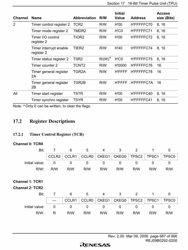
Section 17 16-Bit Timer Pulse Unit (TPU)
Rev. 2.00 Mar 09, 2006 page 687 of 906REJ09B0292-0200
Channel Name Abbreviation R/WInitialValue Address
Accesssize (Bits)
2 Timer control register 2 TCR2 R/W H'00 H'FFFFFC70 8, 16
Timer mode register 2 TMDR2 R/W H'C0 H'FFFFFC71 8, 16
Timer I/O controlregister 2
TIOR2 R/W H'00 H'FFFFFC72 8, 16
Timer interrupt enableregister 2
TIER2 R/W H'40 H'FFFFFC74 8, 16
Timer status register 2 TSR2 R/(W)* H'C0 H'FFFFFC75 8, 16
Timer counter 2 TCNT2 R/W H'0000 H'FFFFFC76 16
Timer general register2A
TGR2A R/W H'FFFF H'FFFFFC78 16
Timer general register2B
TGR2B R/W H'FFFF H'FFFFFC7A 16
All Timer start register TSTR R/W H'00 H'FFFFFC40 8, 16
Timer synchro register TSYR R/W H'00 H'FFFFFC41 8, 16Note: * Only 0 can be written, to clear the flags.
17.2 Register Descriptions
17.2.1 Timer Control Register (TCR)
Channel 0: TCR0Bit: 7 6 5 4 3 2 1 0
CCLR2 CCLR1 CCLR0 CKEG1 CKEG0 TPSC2 TPSC1 TPSC0
Initial value: 0 0 0 0 0 0 0 0
R/W: R/W R/W R/W R/W R/W R/W R/W R/W
Channel 1: TCR1Channel 2: TCR2
Bit: 7 6 5 4 3 2 1 0
� CCLR1 CCLR0 CKEG1 CKEG0 TPSC2 TPSC1 TPSC0
Initial value: 0 0 0 0 0 0 0 0
R/W: R R/W R/W R/W R/W R/W R/W R/W

Section 17 16-Bit Timer Pulse Unit (TPU)
Rev. 2.00 Mar 09, 2006 page 688 of 906REJ09B0292-0200
The TCR registers are 8-bit registers that control the TCNT channels. The TPU has three TCRregisters, one for each of channels 0 to 2. The TCR registers are initialized to H'00 by a reset.
TCNT operation should be stopped when making TCR settings.
Bits 7 to 5�Counter Clear 2 to 0 (CCLR2 to CCLR0): These bits select the TCNT counterclearing source.
ChannelBit 7:CCLR2
Bit 6:CCLR1
Bit 5:CCLR0 Description
0 0 0 0 TCNT clearing disabled (Initial value)1 TCNT cleared by TGRA compare match/input
capture1 0 TCNT cleared by TGRB compare match/input
capture1 TCNT cleared by counter clearing for another
channel performing synchronousclearing/synchronous operation*1
1 0 0 TCNT clearing disabled1 TCNT cleared by TGRC compare match/input
capture*2
1 0 TCNT cleared by TGRD compare match/inputcapture*2
1 TCNT cleared by counter clearing for anotherchannel performing synchronousclearing/synchronous operation*1
ChannelBit 7:Reserved*3
Bit 6:CCLR1
Bit 5:CCLR0 Description
1, 2 0 0 0 TCNT clearing disabled (Initial value)1 TCNT cleared by TGRA compare match/input
capture1 0 TCNT cleared by TGRB compare match/input
capture1 TCNT cleared by counter clearing for another
channel performing synchronous clearing/synchronous operation*1
Notes: 1. Synchronous operation setting is performed by setting the SYNC bit in TSYR to 1.2. When TGRC or TGRD is used as a buffer register, TCNT is not cleared because the
buffer register setting has priority, and compare match/input capture does not occur.3. Bit 7 is reserved in channels 1and 2. It is always read as 0. The write value should
always be 0.
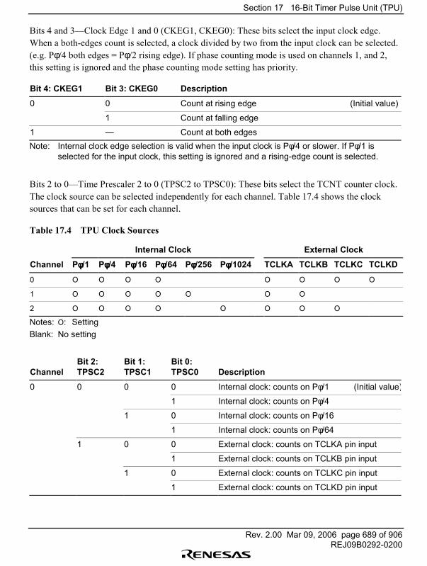
Section 17 16-Bit Timer Pulse Unit (TPU)
Rev. 2.00 Mar 09, 2006 page 689 of 906REJ09B0292-0200
Bits 4 and 3�Clock Edge 1 and 0 (CKEG1, CKEG0): These bits select the input clock edge.When a both-edges count is selected, a clock divided by two from the input clock can be selected.(e.g. Pφ/4 both edges = Pφ/2 rising edge). If phase counting mode is used on channels 1, and 2,this setting is ignored and the phase counting mode setting has priority.
Bit 4: CKEG1 Bit 3: CKEG0 Description
0 0 Count at rising edge (Initial value)
1 Count at falling edge
1 � Count at both edgesNote: Internal clock edge selection is valid when the input clock is Pφ/4 or slower. If Pφ/1 is
selected for the input clock, this setting is ignored and a rising-edge count is selected.
Bits 2 to 0�Time Prescaler 2 to 0 (TPSC2 to TPSC0): These bits select the TCNT counter clock.The clock source can be selected independently for each channel. Table 17.4 shows the clocksources that can be set for each channel.
Table 17.4 TPU Clock Sources
Internal Clock External Clock
Channel Pφφφφ/1 Pφφφφ/4 Pφφφφ/16 Pφφφφ/64 Pφφφφ/256 Pφφφφ/1024 TCLKA TCLKB TCLKC TCLKD
0 O O O O O O O O
1 O O O O O O O
2 O O O O O O O O
Notes: O: SettingBlank: No setting
ChannelBit 2:TPSC2
Bit 1:TPSC1
Bit 0:TPSC0 Description
0 0 0 0 Internal clock: counts on Pφ/1 (Initial value)
1 Internal clock: counts on Pφ/4
1 0 Internal clock: counts on Pφ/16
1 Internal clock: counts on Pφ/64
1 0 0 External clock: counts on TCLKA pin input
1 External clock: counts on TCLKB pin input
1 0 External clock: counts on TCLKC pin input
1 External clock: counts on TCLKD pin input
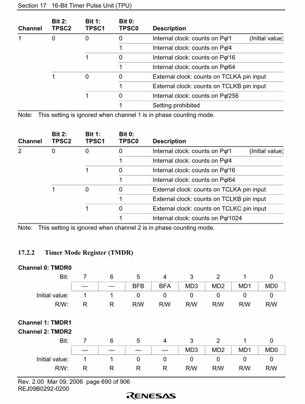
Section 17 16-Bit Timer Pulse Unit (TPU)
Rev. 2.00 Mar 09, 2006 page 690 of 906REJ09B0292-0200
ChannelBit 2:TPSC2
Bit 1:TPSC1
Bit 0:TPSC0 Description
1 0 0 0 Internal clock: counts on Pφ/1 (Initial value)1 Internal clock: counts on Pφ/4
1 0 Internal clock: counts on Pφ/161 Internal clock: counts on Pφ/64
1 0 0 External clock: counts on TCLKA pin input1 External clock: counts on TCLKB pin input
1 0 Internal clock: counts on Pφ/2561 Setting prohibited
Note: This setting is ignored when channel 1 is in phase counting mode.
ChannelBit 2:TPSC2
Bit 1:TPSC1
Bit 0:TPSC0 Description
2 0 0 0 Internal clock: counts on Pφ/1 (Initial value)1 Internal clock: counts on Pφ/4
1 0 Internal clock: counts on Pφ/161 Internal clock: counts on Pφ/64
1 0 0 External clock: counts on TCLKA pin input1 External clock: counts on TCLKB pin input
1 0 External clock: counts on TCLKC pin input1 Internal clock: counts on Pφ/1024
Note: This setting is ignored when channel 2 is in phase counting mode.
17.2.2 Timer Mode Register (TMDR)
Channel 0: TMDR0Bit: 7 6 5 4 3 2 1 0
� � BFB BFA MD3 MD2 MD1 MD0Initial value: 1 1 0 0 0 0 0 0
R/W: R R R/W R/W R/W R/W R/W R/W
Channel 1: TMDR1Channel 2: TMDR2
Bit: 7 6 5 4 3 2 1 0� � � � MD3 MD2 MD1 MD0
Initial value: 1 1 0 0 0 0 0 0R/W: R R R R R/W R/W R/W R/W

Section 17 16-Bit Timer Pulse Unit (TPU)
Rev. 2.00 Mar 09, 2006 page 691 of 906REJ09B0292-0200
The TMDR registers are 8-bit readable/writable registers that are used to set the operating modefor each channel. The TPU has three TMDR registers, one for each channel. The TMDR registersare initialized to H'C0 by a reset.
TCNT operation should be stopped when making TMDR settings.
Bits 7 and 6�Reserved: These bits are always read as 1. The write value should always be 1.
Bit 5�Buffer Operation B (BFB): Specifies whether TGRB is to operate in the normal way, orTGRB and TGRD are to be used together for buffer operation. When TGRD is used as a bufferregister, TGRD input capture/output compare is not generated.
In channels 1 and 2, which have no TGRD, bit 5 is reserved. It is always read as 0 and cannot bemodified.
Bit 5: BFB Description
0 TGRB operates normally (Initial value)
1 TGRB and TGRD used together for buffer operation
Bit 4�Buffer Operation A (BFA): Specifies whether TGRA is to operate in the normal way, orTGRA and TGRC are to be used together for buffer operation. When TGRC is used as a bufferregister, TGRC input capture/output compare is not generated.
In channels 1 and 2, which have no TGRC, bit 4 is reserved. It is always read as 0 and cannot bemodified.
Bit 4: BFA Description
0 TGRA operates normally (Initial value)
1 TGRA and TGRC used together for buffer operation

Section 17 16-Bit Timer Pulse Unit (TPU)
Rev. 2.00 Mar 09, 2006 page 692 of 906REJ09B0292-0200
Bits 3 to 0�Modes 3 to 0 (MD3 to MD0): These bits are used to set the timer operating mode.
Bit 3:MD3*1
Bit 2:MD2*2
Bit 1:MD1
Bit 0:MD0 Description
0 0 0 0 Normal operation (Initial value)
1 Reserved
1 0 PWM mode 1
1 PWM mode 2
1 0 0 Phase counting mode 1
1 Phase counting mode 2
1 0 Phase counting mode 3
1 Phase counting mode 4
1 * * * �*: Don�t care
Notes: 1. MD3 is a reserved bit. In a write, it should always be written with 0.2. Phase counting mode cannot be set for channel 0. In this case, 0 should always be
written to MD2.
17.2.3 Timer I/O Control Register (TIOR)
Channel 0: TIOR0HChannel 1: TIOR1Channel 2: TIOR2
Bit: 7 6 5 4 3 2 1 0
IOB3 IOB2 IOB1 IOB0 IOA3 IOA2 IOA1 IOA0
Initial value: 0 0 0 0 0 0 0 0
R/W: R/W R/W R/W R/W R/W R/W R/W R/W
Channel 0: TIOR0LBit: 7 6 5 4 3 2 1 0
IOD3 IOD2 IOD1 IOD0 IOC3 IOC2 IOC1 IOC0
Initial value: 0 0 0 0 0 0 0 0
R/W: R/W R/W R/W R/W R/W R/W R/W R/W
Note: When TGRC or TGRD is designated for buffer operation, this setting is invalid and theregister operates as a buffer register.

Section 17 16-Bit Timer Pulse Unit (TPU)
Rev. 2.00 Mar 09, 2006 page 693 of 906REJ09B0292-0200
The TIOR registers are 8-bit registers that control the TGR registers. The TPU has four TIORregisters, two for channel 0 and one each for channels 1, and 2. The TIOR registers are initializedto H'00 by a reset.
Note that TIOR is affected by the TMDR setting.
The initial output specified by TIOR becomes valid when the counter is halted (i.e. when the CSTbit is cleared to 0 in TSTR). In PWM mode 2, the output at the point at which the counter iscleared to 0 is specified.
Bits 7 to 4� I/O Control B3 to B0 (IOB3 to IOB0)I/O Control D3 to D0 (IOD3 to IOD0):
Bits IOB3 to IOB0 specify the function of TGRB.Bits IOD3 to IOD0 specify the function of TGRD.
TIOR0H
ChannelBit 7:IOB3
Bit 6:IOB2
Bit 5:IOB1
Bit 4:IOB0 Description
0 0 0 0 0 TGR0B is Output disabled (Initial value)
1 output Initial output is 0 0 output at compare match
1 0compare output 1 output at compare match
1register
Toggle output at comparematch
1 0 0 Output disabled
1 Initial output is 1 0 output at compare match
1 0 output 1 output at compare match
1 Toggle output at comparematch
1 0 0 0 TGR0B is Capture input Input capture at rising edge
1 input source is Input capture at falling edge
1 *capture TIOCB0 pin
Input capture at both edges
1 * *register
Setting prohibited*: Don�t care
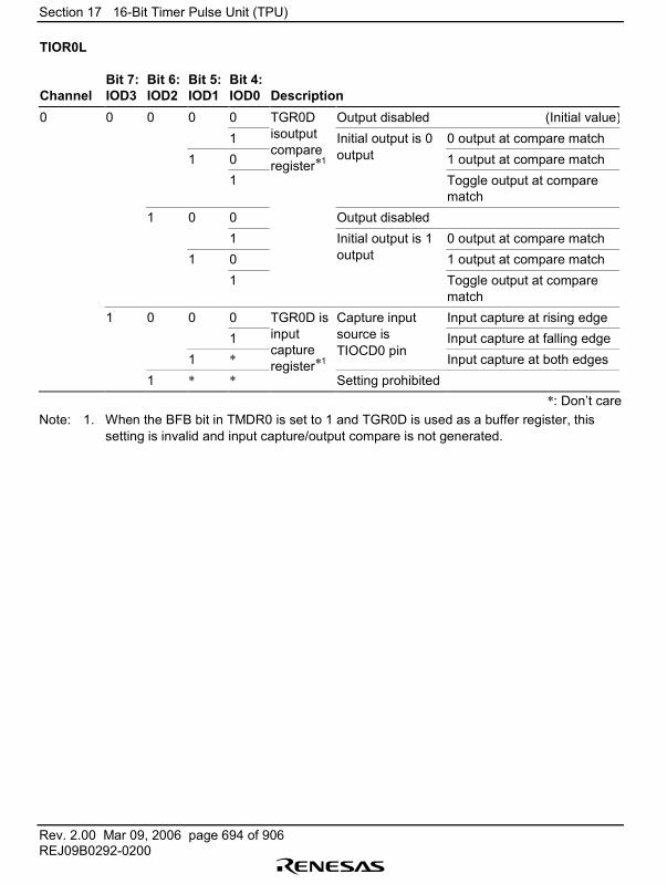
Section 17 16-Bit Timer Pulse Unit (TPU)
Rev. 2.00 Mar 09, 2006 page 694 of 906REJ09B0292-0200
TIOR0L
ChannelBit 7:IOD3
Bit 6:IOD2
Bit 5:IOD1
Bit 4:IOD0 Description
0 0 0 0 0 Output disabled (Initial value)1 Initial output is 0 0 output at compare match
1 0 output 1 output at compare match1
TGR0Disoutputcompareregister*1
Toggle output at comparematch
1 0 0 Output disabled1 Initial output is 1 0 output at compare match
1 0 output 1 output at compare match1 Toggle output at compare
match1 0 0 0 Capture input Input capture at rising edge
1 source is Input capture at falling edge1 *
TIOCD0 pinInput capture at both edges
1 * *
TGR0D isinputcaptureregister*1
Setting prohibited*: Don�t care
Note: 1. When the BFB bit in TMDR0 is set to 1 and TGR0D is used as a buffer register, thissetting is invalid and input capture/output compare is not generated.
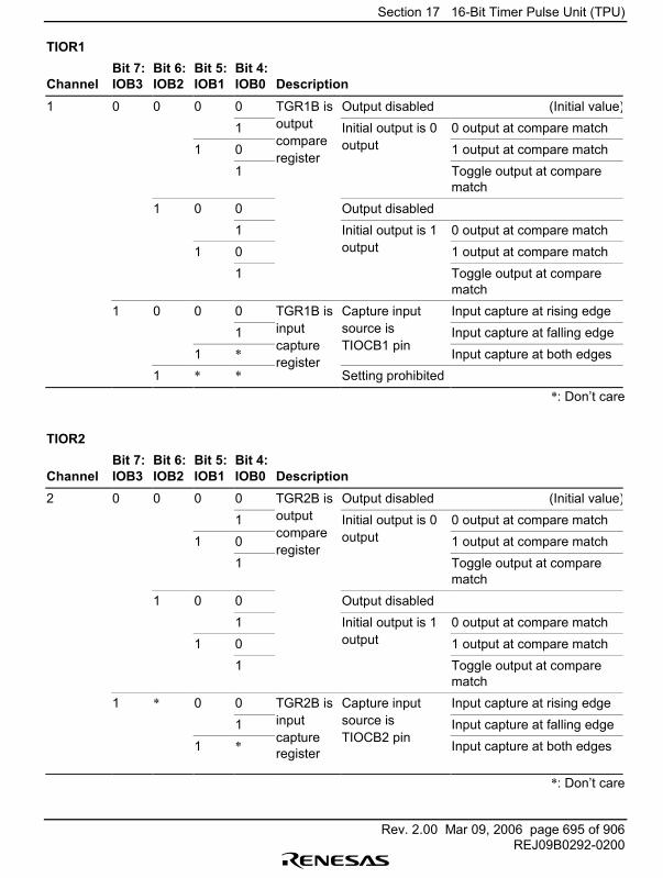
Section 17 16-Bit Timer Pulse Unit (TPU)
Rev. 2.00 Mar 09, 2006 page 695 of 906REJ09B0292-0200
TIOR1
ChannelBit 7:IOB3
Bit 6:IOB2
Bit 5:IOB1
Bit 4:IOB0 Description
1 0 0 0 0 TGR1B is Output disabled (Initial value)1 output Initial output is 0 0 output at compare match
1 0compare output 1 output at compare match
1register
Toggle output at comparematch
1 0 0 Output disabled1 Initial output is 1 0 output at compare match
1 0 output 1 output at compare match1 Toggle output at compare
match1 0 0 0 TGR1B is Capture input Input capture at rising edge
1 input source is Input capture at falling edge1 *
capture TIOCB1 pinInput capture at both edges
1 * *register
Setting prohibited*: Don�t care
TIOR2
ChannelBit 7:IOB3
Bit 6:IOB2
Bit 5:IOB1
Bit 4:IOB0 Description
2 0 0 0 0 TGR2B is Output disabled (Initial value)1 output Initial output is 0 0 output at compare match
1 0compare output 1 output at compare match
1register
Toggle output at comparematch
1 0 0 Output disabled1 Initial output is 1 0 output at compare match
1 0 output 1 output at compare match1 Toggle output at compare
match1 * 0 0 TGR2B is Capture input Input capture at rising edge
1 input source is Input capture at falling edge1 *
captureregister
TIOCB2 pinInput capture at both edges
*: Don�t care
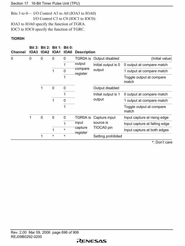
Section 17 16-Bit Timer Pulse Unit (TPU)
Rev. 2.00 Mar 09, 2006 page 696 of 906REJ09B0292-0200
Bits 3 to 0� I/O Control A3 to A0 (IOA3 to IOA0)I/O Control C3 to C0 (IOC3 to IOC0):
IOA3 to IOA0 specify the function of TGRA.IOC3 to IOC0 specify the function of TGRC.
TIOR0H
ChannelBit 3:IOA3
Bit 2:IOA2
Bit 1:IOA1
Bit 0:IOA0 Description
0 0 0 0 0 TGR0A is Output disabled (Initial value)
1 output Initial output is 0 0 output at compare match
1 0compare output 1 output at compare match
1register
Toggle output at comparematch
1 0 0 Output disabled
1 Initial output is 1 0 output at compare match
1 0 output 1 output at compare match
1 Toggle output at comparematch
1 0 0 0 TGR0A is Capture input Input capture at rising edge
1 input source is Input capture at falling edge
1 *capture TIOCA0 pin
Input capture at both edges
1 * *register
Setting prohibited*: Don�t care
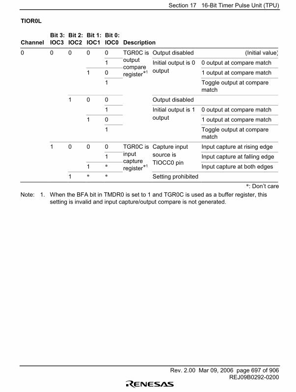
Section 17 16-Bit Timer Pulse Unit (TPU)
Rev. 2.00 Mar 09, 2006 page 697 of 906REJ09B0292-0200
TIOR0L
ChannelBit 3:IOC3
Bit 2:IOC2
Bit 1:IOC1
Bit 0:IOC0 Description
0 0 0 0 0 Output disabled (Initial value)
1 Initial output is 0 0 output at compare match
1 0 output 1 output at compare match
1
TGR0C isoutputcompareregister*1
Toggle output at comparematch
1 0 0 Output disabled
1 Initial output is 1 0 output at compare match
1 0 output 1 output at compare match
1 Toggle output at comparematch
1 0 0 0 Capture input Input capture at rising edge
1 source is Input capture at falling edge
1 *TIOCC0 pin
Input capture at both edges
1 * *
TGR0C isinputcaptureregister*1
Setting prohibited*: Don�t care
Note: 1. When the BFA bit in TMDR0 is set to 1 and TGR0C is used as a buffer register, thissetting is invalid and input capture/output compare is not generated.
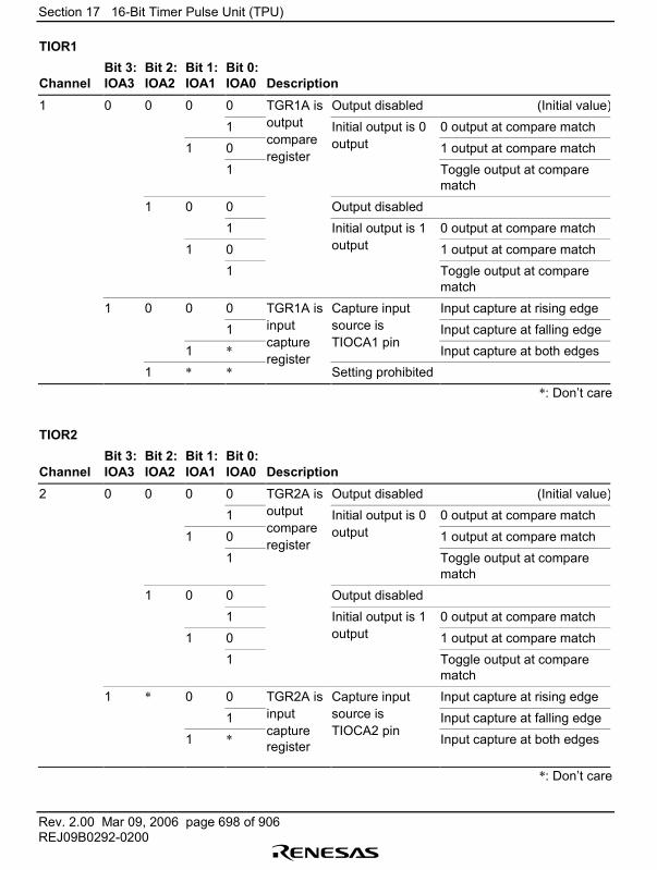
Section 17 16-Bit Timer Pulse Unit (TPU)
Rev. 2.00 Mar 09, 2006 page 698 of 906REJ09B0292-0200
TIOR1
ChannelBit 3:IOA3
Bit 2:IOA2
Bit 1:IOA1
Bit 0:IOA0 Description
1 0 0 0 0 TGR1A is Output disabled (Initial value)1 output Initial output is 0 0 output at compare match
1 0compare output 1 output at compare match
1register
Toggle output at comparematch
1 0 0 Output disabled1 Initial output is 1 0 output at compare match
1 0 output 1 output at compare match1 Toggle output at compare
match1 0 0 0 TGR1A is Capture input Input capture at rising edge
1 input source is Input capture at falling edge1 *
capture TIOCA1 pinInput capture at both edges
1 * *register
Setting prohibited*: Don�t care
TIOR2
ChannelBit 3:IOA3
Bit 2:IOA2
Bit 1:IOA1
Bit 0:IOA0 Description
2 0 0 0 0 TGR2A is Output disabled (Initial value)1 output Initial output is 0 0 output at compare match
1 0compare output 1 output at compare match
1register
Toggle output at comparematch
1 0 0 Output disabled1 Initial output is 1 0 output at compare match
1 0 output 1 output at compare match1 Toggle output at compare
match1 * 0 0 TGR2A is Capture input Input capture at rising edge
1 input source is Input capture at falling edge1 *
captureregister
TIOCA2 pinInput capture at both edges
*: Don�t care

Section 17 16-Bit Timer Pulse Unit (TPU)
Rev. 2.00 Mar 09, 2006 page 699 of 906REJ09B0292-0200
17.2.4 Timer Interrupt Enable Register (TIER)
Channel 0: TIER0Bit: 7 6 5 4 3 2 1 0
� � � TCIEV TGIED TGIEC TGIEB TGIEA
Initial value: 0 1 0 0 0 0 0 0
R/W: R R R R/W R/W R/W R/W R/W
Channel 1: TIER1Channel 2: TIER2
Bit: 7 6 5 4 3 2 1 0
� � TCIEU TCIEV � � TGIEB TGIEA
Initial value: 0 1 0 0 0 0 0 0
R/W: R R R/W R/W R R R/W R/W
The TIER registers are 8-bit registers that control enabling or disabling of interrupt requests foreach channel. The TPU has three TIER registers, one for each channel. The TIER registers areinitialized to H'40 by a reset.
Bit 7�Reserved: This bit is always read as 0. The write value should always be 0.
Bit 6�Reserved: This bit is always read as 1. The write value should always be 1.
Bit 5�Underflow Interrupt Enable (TCIEU): Enables or disables interrupt requests (TCIU) by theTCFU flag when the TCFU flag in TSR is set to 1 in channels 1 and 2.
In channel 0, bit 5 is reserved. It is always read as 0 and cannot be modified.
Bit 5: TCIEU Description
0 Interrupt requests (TCIU) by TCFU disabled (Initial value)
1 Interrupt requests (TCIU) by TCFU enabled
Bit 4�Overflow Interrupt Enable (TCIEV): Enables or disables interrupt requests (TCIV) by theTCFV flag when the TCFV flag in TSR is set to 1.
Bit 4: TCIEV Description0 Interrupt requests (TCIV) by TCFV disabled (Initial value)1 Interrupt requests (TCIV) by TCFV enabled
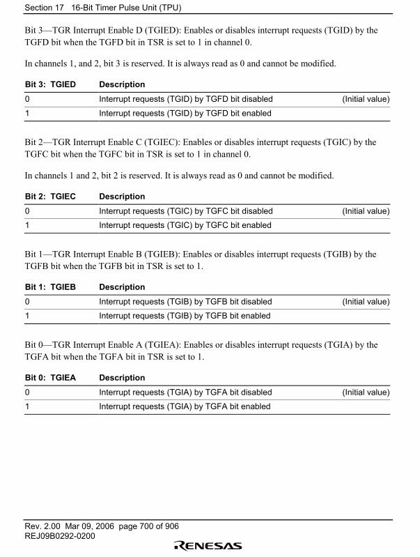
Section 17 16-Bit Timer Pulse Unit (TPU)
Rev. 2.00 Mar 09, 2006 page 700 of 906REJ09B0292-0200
Bit 3�TGR Interrupt Enable D (TGIED): Enables or disables interrupt requests (TGID) by theTGFD bit when the TGFD bit in TSR is set to 1 in channel 0.
In channels 1, and 2, bit 3 is reserved. It is always read as 0 and cannot be modified.
Bit 3: TGIED Description
0 Interrupt requests (TGID) by TGFD bit disabled (Initial value)
1 Interrupt requests (TGID) by TGFD bit enabled
Bit 2�TGR Interrupt Enable C (TGIEC): Enables or disables interrupt requests (TGIC) by theTGFC bit when the TGFC bit in TSR is set to 1 in channel 0.
In channels 1 and 2, bit 2 is reserved. It is always read as 0 and cannot be modified.
Bit 2: TGIEC Description
0 Interrupt requests (TGIC) by TGFC bit disabled (Initial value)
1 Interrupt requests (TGIC) by TGFC bit enabled
Bit 1�TGR Interrupt Enable B (TGIEB): Enables or disables interrupt requests (TGIB) by theTGFB bit when the TGFB bit in TSR is set to 1.
Bit 1: TGIEB Description
0 Interrupt requests (TGIB) by TGFB bit disabled (Initial value)
1 Interrupt requests (TGIB) by TGFB bit enabled
Bit 0�TGR Interrupt Enable A (TGIEA): Enables or disables interrupt requests (TGIA) by theTGFA bit when the TGFA bit in TSR is set to 1.
Bit 0: TGIEA Description
0 Interrupt requests (TGIA) by TGFA bit disabled (Initial value)
1 Interrupt requests (TGIA) by TGFA bit enabled

Section 17 16-Bit Timer Pulse Unit (TPU)
Rev. 2.00 Mar 09, 2006 page 701 of 906REJ09B0292-0200
17.2.5 Timer Status Register (TSR)
Channel 0: TSR0Bit: 7 6 5 4 3 2 1 0
� � � TCFV TGFD TGFC TGFB TGFA
Initial value: 1 1 0 0 0 0 0 0
R/W: R R R R/(W)* R/(W)* R/(W)* R/(W)* R/(W)*
Note: * Only 0 can be written, to clear the flags.
Channel 1: TSR1Channel 2: TSR2
Bit: 7 6 5 4 3 2 1 0
TCFD � TCFU TCFV � � TGFB TGFA
Initial value: 1 1 0 0 0 0 0 0
R/W: R R R/(W)* R/(W)* R R R/(W)* R/(W)*
Note: * Only 0 can be written, to clear the flags.
The TSR registers are 8-bit registers that indicate the status of each channel. The TPU has threeTSR registers, one for each channel. The TSR registers are initialized to H'C0 by a reset.
Bit 7�Count Direction Flag (TCFD): Status flag that shows the direction in which TCNT countsin channels 1, and 2.
In channel 0, bit 7 is reserved. It is always read as 1 and cannot be modified.
Bit 7: TCFD Description
0 TCNT counts down
1 TCNT counts up (Initial value)
Bit 6�Reserved: This bit is always read as 0. The write value should always be 0.
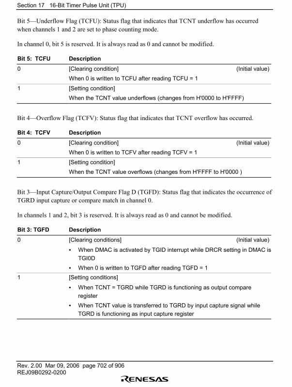
Section 17 16-Bit Timer Pulse Unit (TPU)
Rev. 2.00 Mar 09, 2006 page 702 of 906REJ09B0292-0200
Bit 5�Underflow Flag (TCFU): Status flag that indicates that TCNT underflow has occurredwhen channels 1 and 2 are set to phase counting mode.
In channel 0, bit 5 is reserved. It is always read as 0 and cannot be modified.
Bit 5: TCFU Description
0 [Clearing condition] (Initial value)
When 0 is written to TCFU after reading TCFU = 1
1 [Setting condition]
When the TCNT value underflows (changes from H'0000 to H'FFFF)
Bit 4�Overflow Flag (TCFV): Status flag that indicates that TCNT overflow has occurred.
Bit 4: TCFV Description
0 [Clearing condition] (Initial value)
When 0 is written to TCFV after reading TCFV = 1
1 [Setting condition]
When the TCNT value overflows (changes from H'FFFF to H'0000 )
Bit 3�Input Capture/Output Compare Flag D (TGFD): Status flag that indicates the occurrence ofTGRD input capture or compare match in channel 0.
In channels 1 and 2, bit 3 is reserved. It is always read as 0 and cannot be modified.
Bit 3: TGFD Description
0 [Clearing conditions] (Initial value)
• When DMAC is activated by TGID interrupt while DRCR setting in DMAC isTGI0D
• When 0 is written to TGFD after reading TGFD = 11 [Setting conditions]
• When TCNT = TGRD while TGRD is functioning as output compareregister
• When TCNT value is transferred to TGRD by input capture signal whileTGRD is functioning as input capture register
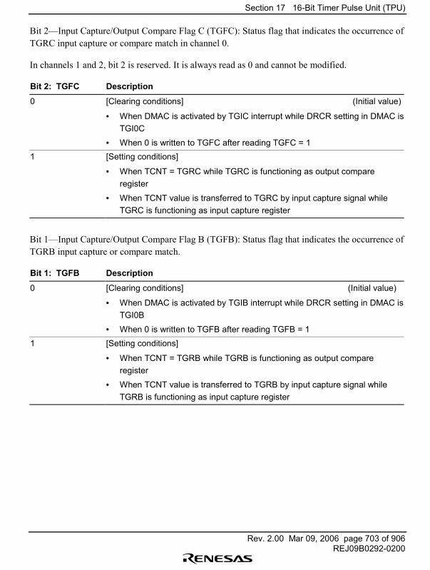
Section 17 16-Bit Timer Pulse Unit (TPU)
Rev. 2.00 Mar 09, 2006 page 703 of 906REJ09B0292-0200
Bit 2�Input Capture/Output Compare Flag C (TGFC): Status flag that indicates the occurrence ofTGRC input capture or compare match in channel 0.
In channels 1 and 2, bit 2 is reserved. It is always read as 0 and cannot be modified.
Bit 2: TGFC Description
0 [Clearing conditions] (Initial value)
• When DMAC is activated by TGIC interrupt while DRCR setting in DMAC isTGI0C
• When 0 is written to TGFC after reading TGFC = 11 [Setting conditions]
• When TCNT = TGRC while TGRC is functioning as output compareregister
• When TCNT value is transferred to TGRC by input capture signal whileTGRC is functioning as input capture register
Bit 1�Input Capture/Output Compare Flag B (TGFB): Status flag that indicates the occurrence ofTGRB input capture or compare match.
Bit 1: TGFB Description
0 [Clearing conditions] (Initial value)
• When DMAC is activated by TGIB interrupt while DRCR setting in DMAC isTGI0B
• When 0 is written to TGFB after reading TGFB = 11 [Setting conditions]
• When TCNT = TGRB while TGRB is functioning as output compareregister
• When TCNT value is transferred to TGRB by input capture signal whileTGRB is functioning as input capture register
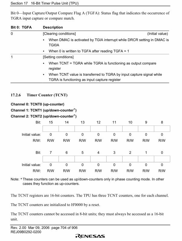
Section 17 16-Bit Timer Pulse Unit (TPU)
Rev. 2.00 Mar 09, 2006 page 704 of 906REJ09B0292-0200
Bit 0�Input Capture/Output Compare Flag A (TGFA): Status flag that indicates the occurrence ofTGRA input capture or compare match.
Bit 0: TGFA Description
0 [Clearing conditions] (Initial value)
• When DMAC is activated by TGIA interrupt while DRCR setting in DMAC isTGI0A
• When 0 is written to TGFA after reading TGFA = 11 [Setting conditions]
• When TCNT = TGRA while TGRA is functioning as output compareregister
• When TCNT value is transferred to TGRA by input capture signal whileTGRA is functioning as input capture register
17.2.6 Timer Counter (TCNT)
Channel 0: TCNT0 (up-counter)Channel 1: TCNT1 (up/down-counter*)Channel 2: TCNT2 (up/down-counter*)
Bit: 15 14 13 12 11 10 9 8
Initial value: 0 0 0 0 0 0 0 0
R/W: R/W R/W R/W R/W R/W R/W R/W R/W
Bit: 7 6 5 4 3 2 1 0
Initial value: 0 0 0 0 0 0 0 0
R/W: R/W R/W R/W R/W R/W R/W R/W R/W
Note: * These counters can be used as up/down-counters only in phase counting mode. In othercases they function as up-counters.
The TCNT registers are 16-bit counters. The TPU has three TCNT counters, one for each channel.
The TCNT counters are initialized to H'0000 by a reset.
The TCNT counters cannot be accessed in 8-bit units; they must always be accessed as a 16-bitunit.
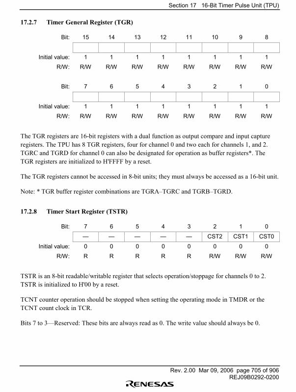
Section 17 16-Bit Timer Pulse Unit (TPU)
Rev. 2.00 Mar 09, 2006 page 705 of 906REJ09B0292-0200
17.2.7 Timer General Register (TGR)
Bit: 15 14 13 12 11 10 9 8
Initial value: 1 1 1 1 1 1 1 1
R/W: R/W R/W R/W R/W R/W R/W R/W R/W
Bit: 7 6 5 4 3 2 1 0
Initial value: 1 1 1 1 1 1 1 1
R/W: R/W R/W R/W R/W R/W R/W R/W R/W
The TGR registers are 16-bit registers with a dual function as output compare and input captureregisters. The TPU has 8 TGR registers, four for channel 0 and two each for channels 1, and 2.TGRC and TGRD for channel 0 can also be designated for operation as buffer registers*. TheTGR registers are initialized to H'FFFF by a reset.
The TGR registers cannot be accessed in 8-bit units; they must always be accessed as a 16-bit unit.
Note: * TGR buffer register combinations are TGRA�TGRC and TGRB�TGRD.
17.2.8 Timer Start Register (TSTR)
Bit: 7 6 5 4 3 2 1 0
� � � � � CST2 CST1 CST0
Initial value: 0 0 0 0 0 0 0 0
R/W: R R R R R R/W R/W R/W
TSTR is an 8-bit readable/writable register that selects operation/stoppage for channels 0 to 2.TSTR is initialized to H'00 by a reset.
TCNT counter operation should be stopped when setting the operating mode in TMDR or theTCNT count clock in TCR.
Bits 7 to 3�Reserved: These bits are always read as 0. The write value should always be 0.
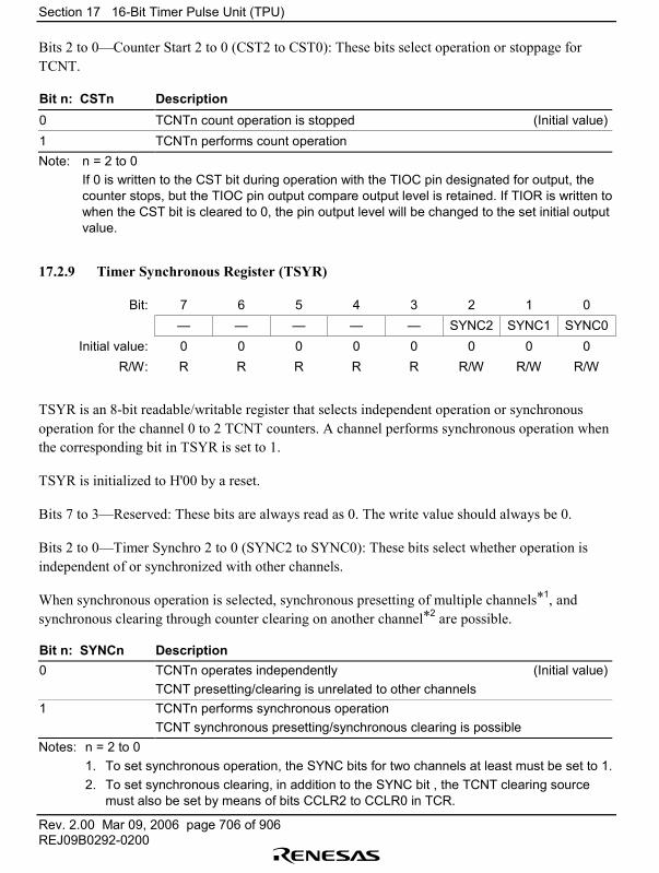
Section 17 16-Bit Timer Pulse Unit (TPU)
Rev. 2.00 Mar 09, 2006 page 706 of 906REJ09B0292-0200
Bits 2 to 0�Counter Start 2 to 0 (CST2 to CST0): These bits select operation or stoppage forTCNT.
Bit n: CSTn Description0 TCNTn count operation is stopped (Initial value)1 TCNTn performs count operationNote: n = 2 to 0
If 0 is written to the CST bit during operation with the TIOC pin designated for output, thecounter stops, but the TIOC pin output compare output level is retained. If TIOR is written towhen the CST bit is cleared to 0, the pin output level will be changed to the set initial outputvalue.
17.2.9 Timer Synchronous Register (TSYR)
Bit: 7 6 5 4 3 2 1 0� � � � � SYNC2 SYNC1 SYNC0
Initial value: 0 0 0 0 0 0 0 0R/W: R R R R R R/W R/W R/W
TSYR is an 8-bit readable/writable register that selects independent operation or synchronousoperation for the channel 0 to 2 TCNT counters. A channel performs synchronous operation whenthe corresponding bit in TSYR is set to 1.
TSYR is initialized to H'00 by a reset.
Bits 7 to 3�Reserved: These bits are always read as 0. The write value should always be 0.
Bits 2 to 0�Timer Synchro 2 to 0 (SYNC2 to SYNC0): These bits select whether operation isindependent of or synchronized with other channels.
When synchronous operation is selected, synchronous presetting of multiple channels*1, andsynchronous clearing through counter clearing on another channel*2 are possible.
Bit n: SYNCn Description0 TCNTn operates independently (Initial value)
TCNT presetting/clearing is unrelated to other channels 1 TCNTn performs synchronous operation
TCNT synchronous presetting/synchronous clearing is possibleNotes: n = 2 to 0
1. To set synchronous operation, the SYNC bits for two channels at least must be set to 1.2. To set synchronous clearing, in addition to the SYNC bit , the TCNT clearing source
must also be set by means of bits CCLR2 to CCLR0 in TCR.
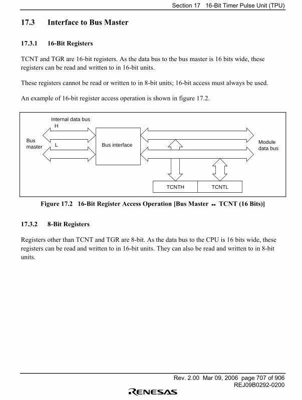
Section 17 16-Bit Timer Pulse Unit (TPU)
Rev. 2.00 Mar 09, 2006 page 707 of 906REJ09B0292-0200
17.3 Interface to Bus Master
17.3.1 16-Bit Registers
TCNT and TGR are 16-bit registers. As the data bus to the bus master is 16 bits wide, theseregisters can be read and written to in 16-bit units.
These registers cannot be read or written to in 8-bit units; 16-bit access must always be used.
An example of 16-bit register access operation is shown in figure 17.2.
Bus interface
HInternal data bus
LBusmaster
Moduledata bus
TCNTH TCNTL
Figure 17.2 16-Bit Register Access Operation [Bus Master ↔↔↔↔ TCNT (16 Bits)]
17.3.2 8-Bit Registers
Registers other than TCNT and TGR are 8-bit. As the data bus to the CPU is 16 bits wide, theseregisters can be read and written to in 16-bit units. They can also be read and written to in 8-bitunits.
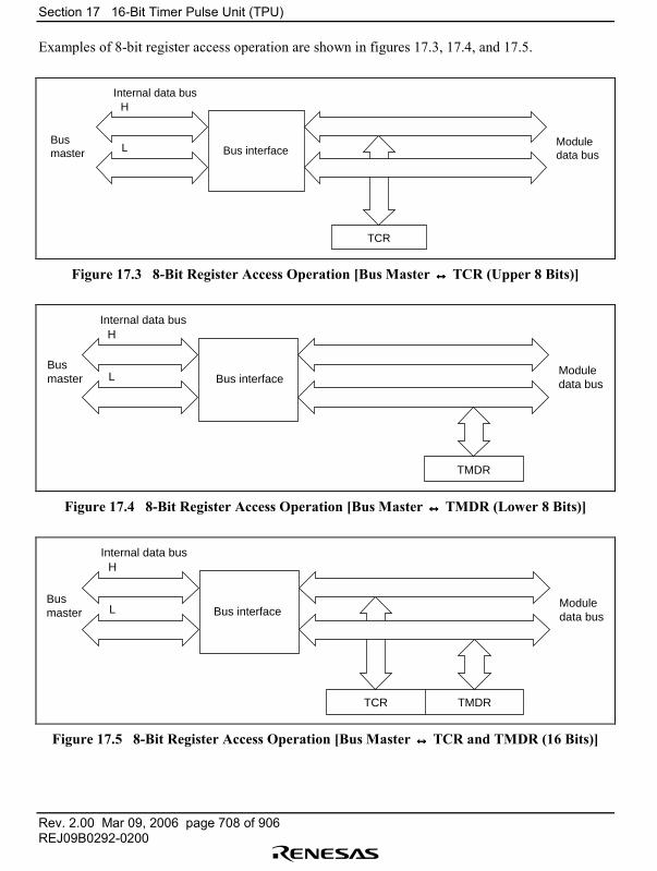
Section 17 16-Bit Timer Pulse Unit (TPU)
Rev. 2.00 Mar 09, 2006 page 708 of 906REJ09B0292-0200
Examples of 8-bit register access operation are shown in figures 17.3, 17.4, and 17.5.
Bus interface
HInternal data bus
L Moduledata bus
TCR
Busmaster
Figure 17.3 8-Bit Register Access Operation [Bus Master ↔↔↔↔ TCR (Upper 8 Bits)]
Bus interface
HInternal data bus
L Moduledata bus
TMDR
Busmaster
Figure 17.4 8-Bit Register Access Operation [Bus Master ↔↔↔↔ TMDR (Lower 8 Bits)]
Bus interface
HInternal data bus
L Moduledata bus
TCR TMDR
Busmaster
Figure 17.5 8-Bit Register Access Operation [Bus Master ↔↔↔↔ TCR and TMDR (16 Bits)]
Section 17 16-Bit Timer Pulse Unit (TPU)
Rev. 2.00 Mar 09, 2006 page 709 of 906REJ09B0292-0200
17.4 Operation
17.4.1 Overview
Operation in each mode is outlined below.
Normal Operation: Each channel has a TCNT and TGR register. TCNT performs up-counting,and is also capable of free-running operation, synchronous counting, and external event counting.
Each TGR can be used as an input capture register or output compare register.
Synchronous Operation: The TCNT counter for a channel designated for synchronous operationby means of TSYR performs synchronous presetting. That is, when TCNT for a channeldesignated for synchronous operation is rewritten, the TCNT counters for the other channels arealso rewritten at the same time. Synchronous clearing of the TCNT counters is also possible bysetting the counter clear bits in TCR for channels designated for synchronous operation.
Buffer Operation
• When TGR is an output compare registerWhen a compare match occurs, the value in the buffer register for the relevant channel istransferred to TGR.
• When TGR is an input capture registerWhen input capture occurs, the value in TCNT is transfer to TGR and the value previouslyheld in TGR is transferred to the buffer register.
PWM Mode: In this mode, a PWM waveform is output. The output level can be set by means ofTIOR. A PWM waveform with a duty of between 0% and 100% can be output, according to thesetting of each TGR register.
Phase Counting Mode: In this mode, TCNT is incremented or decremented by detecting thephases of two clocks input from the external clock input pins in channels 1, and 2. When phasecounting mode is set, the corresponding TCLK pin functions as the clock input, and TCNTperforms up- or down-counting.
This can be used for two-phase encoder pulse input.
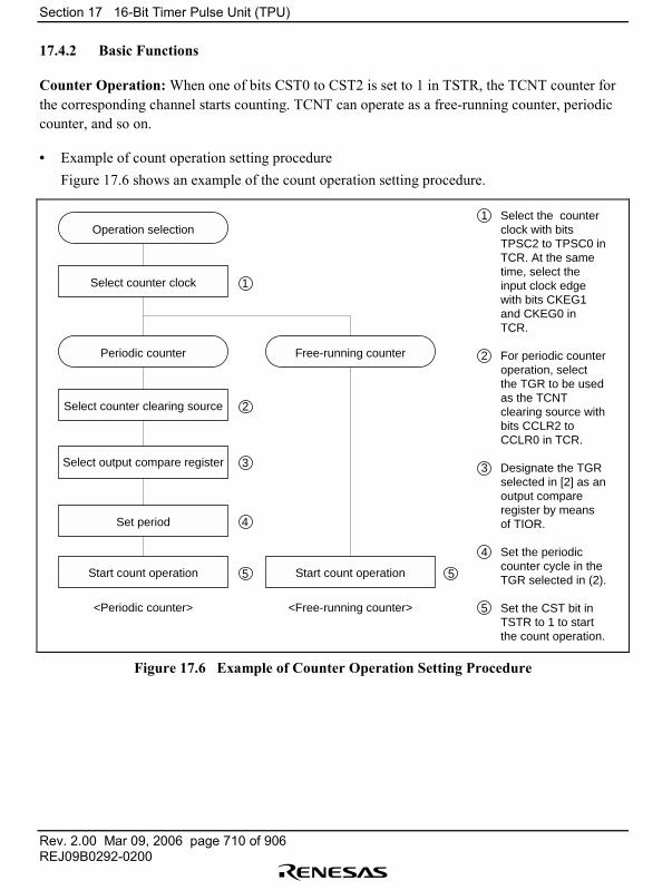
Section 17 16-Bit Timer Pulse Unit (TPU)
Rev. 2.00 Mar 09, 2006 page 710 of 906REJ09B0292-0200
17.4.2 Basic Functions
Counter Operation: When one of bits CST0 to CST2 is set to 1 in TSTR, the TCNT counter forthe corresponding channel starts counting. TCNT can operate as a free-running counter, periodiccounter, and so on.
• Example of count operation setting procedureFigure 17.6 shows an example of the count operation setting procedure.
Select counter clock
Operation selection
Select counter clearing source
Periodic counter
Set period
Start count operation
<Periodic counter>
1
2
4
3
5
Free-running counter
Start count operation
<Free-running counter>
5
1
2
3
4
5
Select the counterclock with bitsTPSC2 to TPSC0 inTCR. At the sametime, select theinput clock edgewith bits CKEG1and CKEG0 inTCR.
For periodic counteroperation, selectthe TGR to be usedas the TCNTclearing source withbits CCLR2 toCCLR0 in TCR.
Designate the TGRselected in [2] as anoutput compareregister by meansof TIOR.
Set the periodiccounter cycle in theTGR selected in (2).
Set the CST bit inTSTR to 1 to startthe count operation.
Select output compare register
Figure 17.6 Example of Counter Operation Setting Procedure
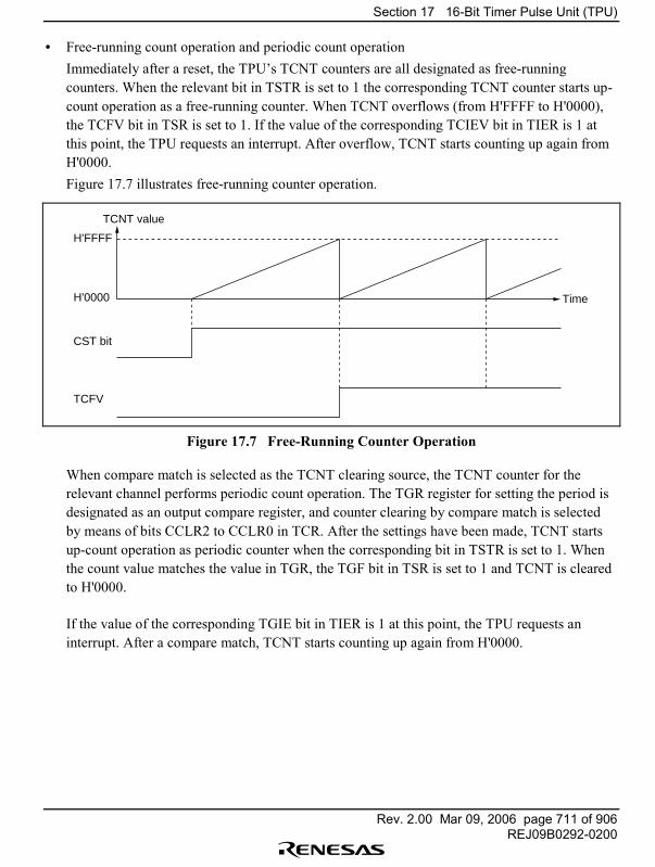
Section 17 16-Bit Timer Pulse Unit (TPU)
Rev. 2.00 Mar 09, 2006 page 711 of 906REJ09B0292-0200
• Free-running count operation and periodic count operationImmediately after a reset, the TPU�s TCNT counters are all designated as free-runningcounters. When the relevant bit in TSTR is set to 1 the corresponding TCNT counter starts up-count operation as a free-running counter. When TCNT overflows (from H'FFFF to H'0000),the TCFV bit in TSR is set to 1. If the value of the corresponding TCIEV bit in TIER is 1 atthis point, the TPU requests an interrupt. After overflow, TCNT starts counting up again fromH'0000.Figure 17.7 illustrates free-running counter operation.
TCNT value
H'FFFF
H'0000
CST bit
TCFV
Time
Figure 17.7 Free-Running Counter Operation
When compare match is selected as the TCNT clearing source, the TCNT counter for therelevant channel performs periodic count operation. The TGR register for setting the period isdesignated as an output compare register, and counter clearing by compare match is selectedby means of bits CCLR2 to CCLR0 in TCR. After the settings have been made, TCNT startsup-count operation as periodic counter when the corresponding bit in TSTR is set to 1. Whenthe count value matches the value in TGR, the TGF bit in TSR is set to 1 and TCNT is clearedto H'0000.
If the value of the corresponding TGIE bit in TIER is 1 at this point, the TPU requests aninterrupt. After a compare match, TCNT starts counting up again from H'0000.
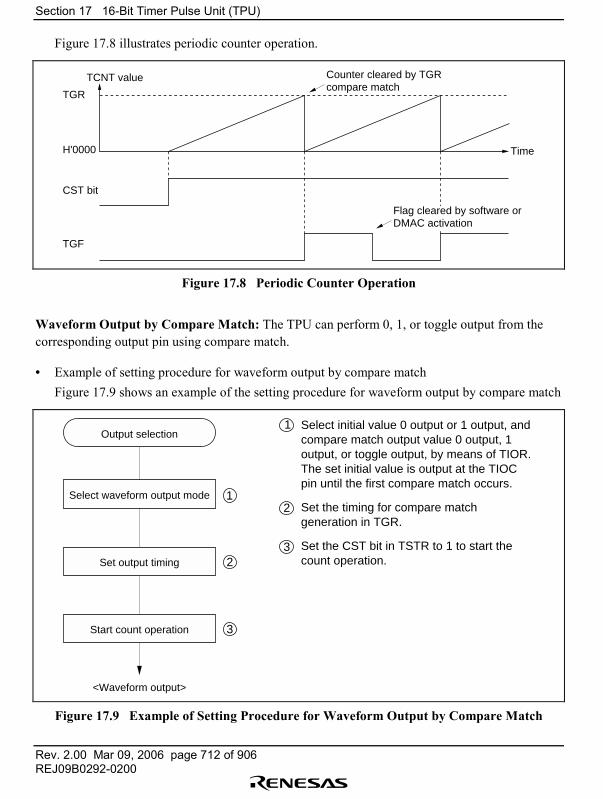
Section 17 16-Bit Timer Pulse Unit (TPU)
Rev. 2.00 Mar 09, 2006 page 712 of 906REJ09B0292-0200
Figure 17.8 illustrates periodic counter operation.
TCNT value
TGR
H'0000
CST bit
TGF
Time
Counter cleared by TGR compare match
Flag cleared by software orDMAC activation
Figure 17.8 Periodic Counter Operation
Waveform Output by Compare Match: The TPU can perform 0, 1, or toggle output from thecorresponding output pin using compare match.
• Example of setting procedure for waveform output by compare matchFigure 17.9 shows an example of the setting procedure for waveform output by compare match
Select waveform output mode
Output selection
Set output timing
Start count operation
<Waveform output>
1
1
2
32
3
Select initial value 0 output or 1 output, and compare match output value 0 output, 1 output, or toggle output, by means of TIOR. The set initial value is output at the TIOC pin until the first compare match occurs.
Set the timing for compare match generation in TGR.
Set the CST bit in TSTR to 1 to start the count operation.
Figure 17.9 Example of Setting Procedure for Waveform Output by Compare Match

Section 17 16-Bit Timer Pulse Unit (TPU)
Rev. 2.00 Mar 09, 2006 page 713 of 906REJ09B0292-0200
• Examples of waveform output operationFigure 17.10 shows an example of 0 output/1 output.In this example TCNT has been designated as a free-running counter, and settings have beenmade so that 1 is output by compare match A, and 0 is output by compare match B. When theset level and the pin level coincide, the pin level does not change.
TCNT value
H'FFFF
H'0000
TIOCA
TIOCB
Time
TGRA
TGRB
No change No change
No change No change
1 output
0 output
Figure 17.10 Example of 0 Output/1 Output Operation
Figure 17.11 shows an example of toggle output.In this example TCNT has been designated as a periodic counter (with counter clearingperformed by compare match B), and settings have been made so that output is toggled by bothcompare match A and compare match B.
TCNT value
H'FFFF
H'0000
TIOCB
TIOCA
Time
TGRB
TGRA
Toggle output
Toggle output
Counter cleared by TGRB compare match
Figure 17.11 Example of Toggle Output Operation
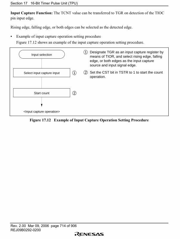
Section 17 16-Bit Timer Pulse Unit (TPU)
Rev. 2.00 Mar 09, 2006 page 714 of 906REJ09B0292-0200
Input Capture Function: The TCNT value can be transferred to TGR on detection of the TIOCpin input edge.
Rising edge, falling edge, or both edges can be selected as the detected edge.
• Example of input capture operation setting procedureFigure 17.12 shows an example of the input capture operation setting procedure.
Select input capture input
Input selection
Start count
<Input capture operation>
1
1
2
2
Designate TGR as an input capture register by means of TIOR, and select rising edge, falling edge, or both edges as the input capture source and input signal edge.
Set the CST bit in TSTR to 1 to start the count operation.
Figure 17.12 Example of Input Capture Operation Setting Procedure
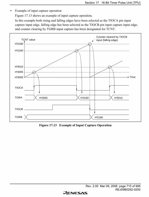
Section 17 16-Bit Timer Pulse Unit (TPU)
Rev. 2.00 Mar 09, 2006 page 715 of 906REJ09B0292-0200
• Example of input capture operationFigure 17.13 shows an example of input capture operation.In this example both rising and falling edges have been selected as the TIOCA pin inputcapture input edge, falling edge has been selected as the TIOCB pin input capture input edge,and counter clearing by TGRB input capture has been designated for TCNT.
TCNT value
H'0180
H'0000
TIOCA
TGRA
Time
H'0010
H'0005
Counter cleared by TIOCBinput (falling edge)
H'0160
H'0005 H'0160 H'0010
TGRB H'0180
TIOCB
Figure 17.13 Example of Input Capture Operation
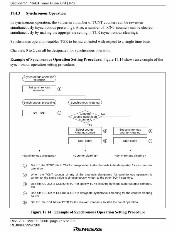
Section 17 16-Bit Timer Pulse Unit (TPU)
Rev. 2.00 Mar 09, 2006 page 716 of 906REJ09B0292-0200
17.4.3 Synchronous Operation
In synchronous operation, the values in a number of TCNT counters can be rewrittensimultaneously (synchronous presetting). Also, a number of TCNT counters can be clearedsimultaneously by making the appropriate setting in TCR (synchronous clearing).
Synchronous operation enables TGR to be incremented with respect to a single time base.
Channels 0 to 2 can all be designated for synchronous operation.
Example of Synchronous Operation Setting Procedure: Figure 17.14 shows an example of thesynchronous operation setting procedure.
Set synchronousoperation
Synchronous operationselection
Set TCNT
Synchronous presetting
<Synchronous presetting>
1
2
Synchronous clearing
Select counterclearing source
<Counter clearing>
3
Start count 5
Set synchronouscounter clearing
<Synchronous clearing>
4
Start count 5
Clearingsource generation
channel?
No
Yes
1
2
3
4
5
Set to 1 the SYNC bits in TSYR corresponding to the channels to be designated for synchronous operation.
When the TCNT counter of any of the channels designated for synchronous operation is written to, the same value is simultaneously written to the other TCNT counters.
Use bits CCLR2 to CCLR0 in TCR to specify TCNT clearing by input capture/output compare, etc.
Use bits CCLR2 to CCLR0 in TCR to designate synchronous clearing for the counter clearing source.
Set to 1 the CST bits in TSTR for the relevant channels, to start the count operation.
Figure 17.14 Example of Synchronous Operation Setting Procedure
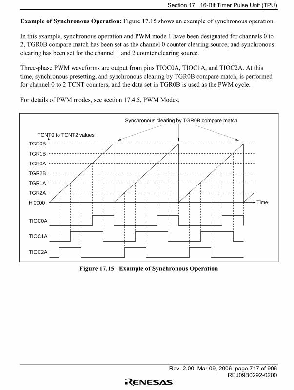
Section 17 16-Bit Timer Pulse Unit (TPU)
Rev. 2.00 Mar 09, 2006 page 717 of 906REJ09B0292-0200
Example of Synchronous Operation: Figure 17.15 shows an example of synchronous operation.
In this example, synchronous operation and PWM mode 1 have been designated for channels 0 to2, TGR0B compare match has been set as the channel 0 counter clearing source, and synchronousclearing has been set for the channel 1 and 2 counter clearing source.
Three-phase PWM waveforms are output from pins TIOC0A, TIOC1A, and TIOC2A. At thistime, synchronous presetting, and synchronous clearing by TGR0B compare match, is performedfor channel 0 to 2 TCNT counters, and the data set in TGR0B is used as the PWM cycle.
For details of PWM modes, see section 17.4.5, PWM Modes.
TCNT0 to TCNT2 values
H'0000
TIOC0A
TIOC1A
Time
TGR0B
Synchronous clearing by TGR0B compare match
TGR2A
TGR1A
TGR2B
TGR0A
TGR1B
TIOC2A
Figure 17.15 Example of Synchronous Operation
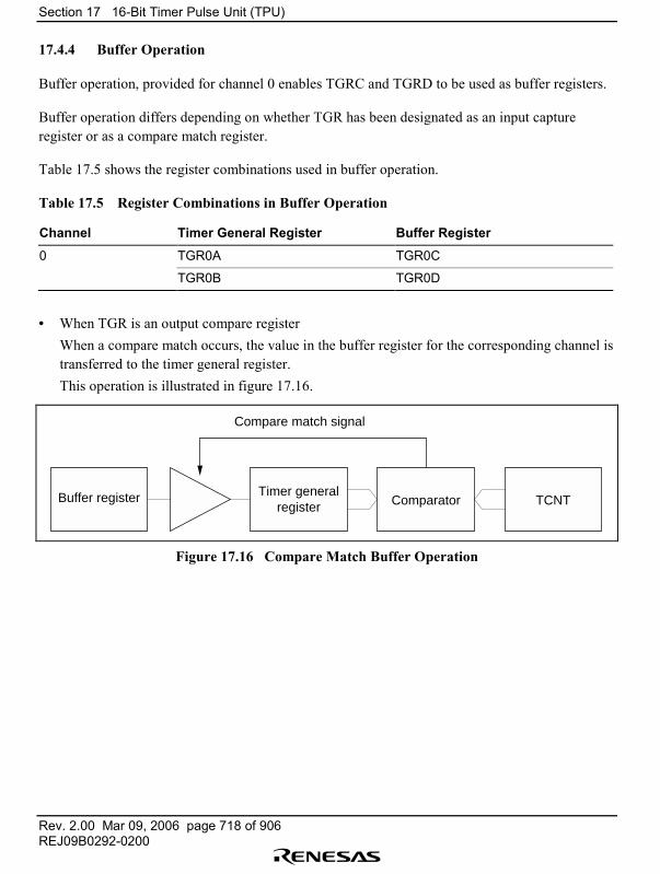
Section 17 16-Bit Timer Pulse Unit (TPU)
Rev. 2.00 Mar 09, 2006 page 718 of 906REJ09B0292-0200
17.4.4 Buffer Operation
Buffer operation, provided for channel 0 enables TGRC and TGRD to be used as buffer registers.
Buffer operation differs depending on whether TGR has been designated as an input captureregister or as a compare match register.
Table 17.5 shows the register combinations used in buffer operation.
Table 17.5 Register Combinations in Buffer Operation
Channel Timer General Register Buffer Register
0 TGR0A TGR0C
TGR0B TGR0D
• When TGR is an output compare registerWhen a compare match occurs, the value in the buffer register for the corresponding channel istransferred to the timer general register.This operation is illustrated in figure 17.16.
Buffer register Timer generalregister TCNTComparator
Compare match signal
Figure 17.16 Compare Match Buffer Operation
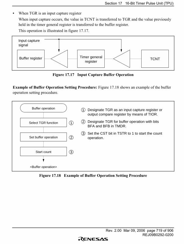
Section 17 16-Bit Timer Pulse Unit (TPU)
Rev. 2.00 Mar 09, 2006 page 719 of 906REJ09B0292-0200
• When TGR is an input capture registerWhen input capture occurs, the value in TCNT is transferred to TGR and the value previouslyheld in the timer general register is transferred to the buffer register.This operation is illustrated in figure 17.17.
Buffer register Timer generalregister
TCNT
Input capturesignal
Figure 17.17 Input Capture Buffer Operation
Example of Buffer Operation Setting Procedure: Figure 17.18 shows an example of the bufferoperation setting procedure.
Select TGR function
Buffer operation
Set buffer operation
Start count
<Buffer operation>
1
1
2
2
3
3
Designate TGR as an input capture register or output compare register by means of TIOR.
Designate TGR for buffer operation with bits BFA and BFB in TMDR.
Set the CST bit in TSTR to 1 to start the count operation.
Figure 17.18 Example of Buffer Operation Setting Procedure
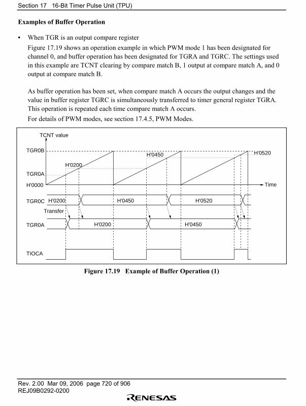
Section 17 16-Bit Timer Pulse Unit (TPU)
Rev. 2.00 Mar 09, 2006 page 720 of 906REJ09B0292-0200
Examples of Buffer Operation
• When TGR is an output compare registerFigure 17.19 shows an operation example in which PWM mode 1 has been designated forchannel 0, and buffer operation has been designated for TGRA and TGRC. The settings usedin this example are TCNT clearing by compare match B, 1 output at compare match A, and 0output at compare match B.
As buffer operation has been set, when compare match A occurs the output changes and thevalue in buffer register TGRC is simultaneously transferred to timer general register TGRA.This operation is repeated each time compare match A occurs.For details of PWM modes, see section 17.4.5, PWM Modes.
TCNT value
TGR0B
H'0000
TGR0C
Time
TGR0A
H'0200 H'0520
TIOCA
H'0200
H'0450 H'0520
H'0450
TGR0A H'0450H'0200
Transfer
Figure 17.19 Example of Buffer Operation (1)
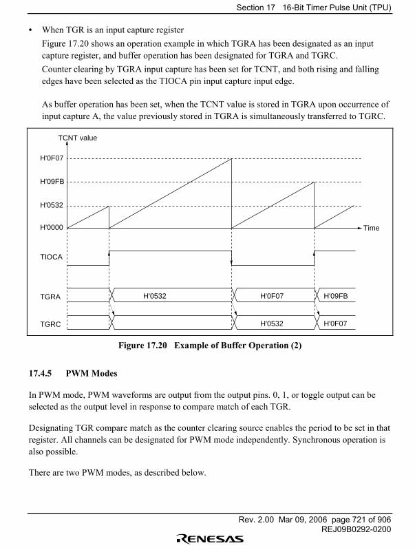
Section 17 16-Bit Timer Pulse Unit (TPU)
Rev. 2.00 Mar 09, 2006 page 721 of 906REJ09B0292-0200
• When TGR is an input capture registerFigure 17.20 shows an operation example in which TGRA has been designated as an inputcapture register, and buffer operation has been designated for TGRA and TGRC.Counter clearing by TGRA input capture has been set for TCNT, and both rising and fallingedges have been selected as the TIOCA pin input capture input edge.
As buffer operation has been set, when the TCNT value is stored in TGRA upon occurrence ofinput capture A, the value previously stored in TGRA is simultaneously transferred to TGRC.
TCNT value
H'09FB
H'0000
TGRC
Time
H'0532
TIOCA
TGRA H'0F07H'0532
H'0F07
H'0532
H'0F07
H'09FB
Figure 17.20 Example of Buffer Operation (2)
17.4.5 PWM Modes
In PWM mode, PWM waveforms are output from the output pins. 0, 1, or toggle output can beselected as the output level in response to compare match of each TGR.
Designating TGR compare match as the counter clearing source enables the period to be set in thatregister. All channels can be designated for PWM mode independently. Synchronous operation isalso possible.
There are two PWM modes, as described below.
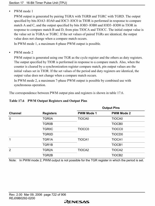
Section 17 16-Bit Timer Pulse Unit (TPU)
Rev. 2.00 Mar 09, 2006 page 722 of 906REJ09B0292-0200
• PWM mode 1PWM output is generated by pairing TGRA with TGRB and TGRC with TGRD. The outputspecified by bits IOA3�IOA0 and IOC3�IOC0 in TIOR is performed in response to comparematch A and C, and the output specified by bits IOB3�IOB0 and IOD3�IOD0 in TIOR inresponse to compare match B and D, from pins TIOCA and TIOCC. The initial output value isthe value set in TGRA or TGRC. If the set values of paired TGRs are identical, the outputvalue does not change when a compare match occurs.In PWM mode 1, a maximum 4-phase PWM output is possible.
• PWM mode 2PWM output is generated using one TGR as the cycle register and the others as duty registers.The output specified by TIOR is performed in response to a compare match. Also, when thecounter is cleared by a synchronization register compare match, pin output values are theinitial values set in TIOR. If the set values of the period and duty registers are identical, theoutput value does not change when a compare match occurs.In PWM mode 2, a maximum 7-phase PWM output is possible by combined use withsynchronous operation.
The correspondence between PWM output pins and registers is shown in table 17.6.
Table 17.6 PWM Output Registers and Output Pins
Output Pins
Channel Registers PWM Mode 1 PWM Mode 2
0 TGR0A TIOCA0 TIOCA0
TGR0B TIOCB0
TGR0C TIOCC0 TIOCC0
TGR0D TIOCD0
1 TGR1A TIOCA1 TIOCA1
TGR1B TIOCB1
2 TGR2A TIOCA2 TIOCA2
TGR2B TIOCB2Note: In PWM mode 2, PWM output is not possible for the TGR register in which the period is set.
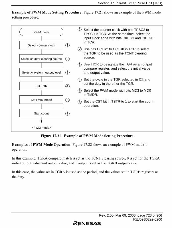
Section 17 16-Bit Timer Pulse Unit (TPU)
Rev. 2.00 Mar 09, 2006 page 723 of 906REJ09B0292-0200
Example of PWM Mode Setting Procedure: Figure 17.21 shows an example of the PWM modesetting procedure.
Select counter clock
PWM mode
Select counter clearing source
Select waveform output level
<PWM mode>
1
1
2
2
3
3
Set TGR 4
4
Set PWM mode 5
5
Start count 6
6
Select the counter clock with bits TPSC2 to TPSC0 in TCR. At the same time, select the input clock edge with bits CKEG1 and CKEG0 in TCR.
Use bits CCLR2 to CCLR0 in TCR to select the TGR to be used as the TCNT clearing source.
Use TIOR to designate the TGR as an output compare register, and select the initial value and output value.
Set the cycle in the TGR selected in [2], and set the duty in the other the TGR.
Select the PWM mode with bits MD3 to MD0 in TMDR.
Set the CST bit in TSTR to 1 to start the count operation.
Figure 17.21 Example of PWM Mode Setting Procedure
Examples of PWM Mode Operation: Figure 17.22 shows an example of PWM mode 1operation.
In this example, TGRA compare match is set as the TCNT clearing source, 0 is set for the TGRAinitial output value and output value, and 1 output is set as the TGRB output value.
In this case, the value set in TGRA is used as the period, and the values set in TGRB registers asthe duty.
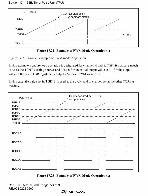
Section 17 16-Bit Timer Pulse Unit (TPU)
Rev. 2.00 Mar 09, 2006 page 724 of 906REJ09B0292-0200
TCNT value
TGRA
H'0000
TIOCA
Time
TGRB
Counter cleared byTGRA compare match
Figure 17.22 Example of PWM Mode Operation (1)
Figure 17.23 shows an example of PWM mode 2 operation.
In this example, synchronous operation is designated for channels 0 and 1, TGR1B compare matchis set as the TCNT clearing source, and 0 is set for the initial output value and 1 for the outputvalue of the other TGR registers, to output a 5-phase PWM waveform.
In this case, the value set in TGR1B is used as the cycle, and the values set in the other TGRs asthe duty.
TCNT value
TGR1B
H'0000
TIOCA0
Counter cleared by TGR1Bcompare match
TGR1ATGR0DTGR0CTGR0BTGR0A
TIOCB0
TIOCC0
TIOCD0
TIOCA1
Figure 17.23 Example of PWM Mode Operation (2)

Section 17 16-Bit Timer Pulse Unit (TPU)
Rev. 2.00 Mar 09, 2006 page 725 of 906REJ09B0292-0200
Figure 17.24 shows examples of PWM waveform output with 0% duty and 100% duty in PWMmode.
TCNT value
TGRA
H'0000
TIOCA
Time
TGRB
0% duty
TGRB rewritten
TGRBrewrittenTGRB rewritten
TCNT value
TGRA
H'0000
TIOCA
Time
TGRB
100% duty
TGRB rewritten
TGRB rewritten
TGRB rewritten
Output does not change when cycle register and duty registercompare matches occur simultaneously
TCNT value
TGRA
H'0000
TIOCA
Time
TGRB
100% duty
TGRB rewritten
TGRB rewritten
TGRB rewritten
Output does not change when cycle register and dutyregister compare matches occur simultaneously
0% duty
Figure 17.24 Example of PWM Mode Operation (3)
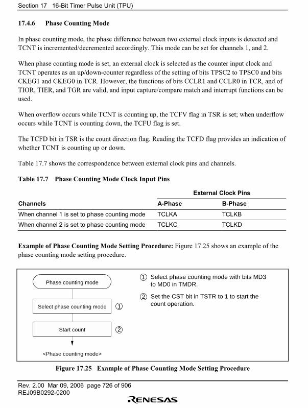
Section 17 16-Bit Timer Pulse Unit (TPU)
Rev. 2.00 Mar 09, 2006 page 726 of 906REJ09B0292-0200
17.4.6 Phase Counting Mode
In phase counting mode, the phase difference between two external clock inputs is detected andTCNT is incremented/decremented accordingly. This mode can be set for channels 1, and 2.
When phase counting mode is set, an external clock is selected as the counter input clock andTCNT operates as an up/down-counter regardless of the setting of bits TPSC2 to TPSC0 and bitsCKEG1 and CKEG0 in TCR. However, the functions of bits CCLR1 and CCLR0 in TCR, and ofTIOR, TIER, and TGR are valid, and input capture/compare match and interrupt functions can beused.
When overflow occurs while TCNT is counting up, the TCFV flag in TSR is set; when underflowoccurs while TCNT is counting down, the TCFU flag is set.
The TCFD bit in TSR is the count direction flag. Reading the TCFD flag provides an indication ofwhether TCNT is counting up or down.
Table 17.7 shows the correspondence between external clock pins and channels.
Table 17.7 Phase Counting Mode Clock Input Pins
External Clock Pins
Channels A-Phase B-Phase
When channel 1 is set to phase counting mode TCLKA TCLKB
When channel 2 is set to phase counting mode TCLKC TCLKD
Example of Phase Counting Mode Setting Procedure: Figure 17.25 shows an example of thephase counting mode setting procedure.
Select phase counting mode
Phase counting mode
Start count
<Phase counting mode>
1
1
2
2
Select phase counting mode with bits MD3 to MD0 in TMDR.
Set the CST bit in TSTR to 1 to start the count operation.
Figure 17.25 Example of Phase Counting Mode Setting Procedure
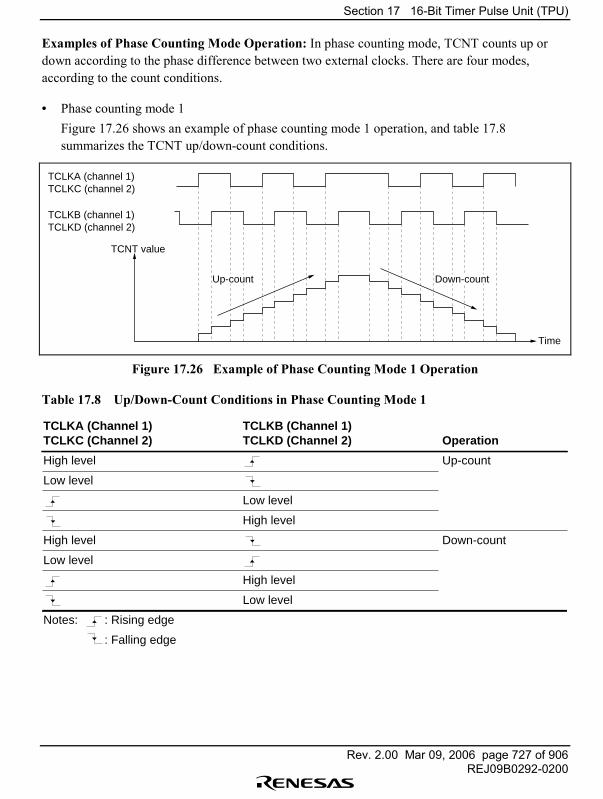
Section 17 16-Bit Timer Pulse Unit (TPU)
Rev. 2.00 Mar 09, 2006 page 727 of 906REJ09B0292-0200
Examples of Phase Counting Mode Operation: In phase counting mode, TCNT counts up ordown according to the phase difference between two external clocks. There are four modes,according to the count conditions.
• Phase counting mode 1Figure 17.26 shows an example of phase counting mode 1 operation, and table 17.8summarizes the TCNT up/down-count conditions.
TCNT value
Time
Down-countUp-count
TCLKA (channel 1)TCLKC (channel 2)
TCLKB (channel 1)TCLKD (channel 2)
Figure 17.26 Example of Phase Counting Mode 1 Operation
Table 17.8 Up/Down-Count Conditions in Phase Counting Mode 1
TCLKA (Channel 1)TCLKC (Channel 2)
High level
Low level
High level
Low level
Notes: : Rising edge
: Falling edge
TCLKB (Channel 1)TCLKD (Channel 2)
Low level
High level
High level
Low level
Operation
Up-count
Down-count
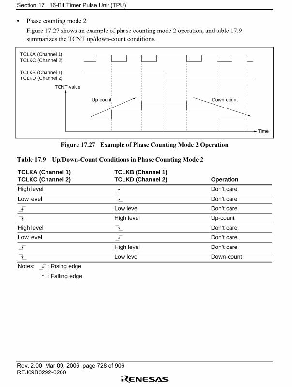
Section 17 16-Bit Timer Pulse Unit (TPU)
Rev. 2.00 Mar 09, 2006 page 728 of 906REJ09B0292-0200
• Phase counting mode 2Figure 17.27 shows an example of phase counting mode 2 operation, and table 17.9summarizes the TCNT up/down-count conditions.
TCNT value
Time
Down-countUp-count
TCLKA (Channel 1)TCLKC (Channel 2)
TCLKB (Channel 1)TCLKD (Channel 2)
Figure 17.27 Example of Phase Counting Mode 2 Operation
Table 17.9 Up/Down-Count Conditions in Phase Counting Mode 2
TCLKA (Channel 1)TCLKC (Channel 2)
High level
Low level
High level
Low level
Notes: : Rising edge
: Falling edge
TCLKB (Channel 1)TCLKD (Channel 2)
Low level
High level
High level
Low level
Operation
Don’t care
Don’t care
Don’t care
Up-count
Don’t care
Don’t care
Don’t care
Down-count
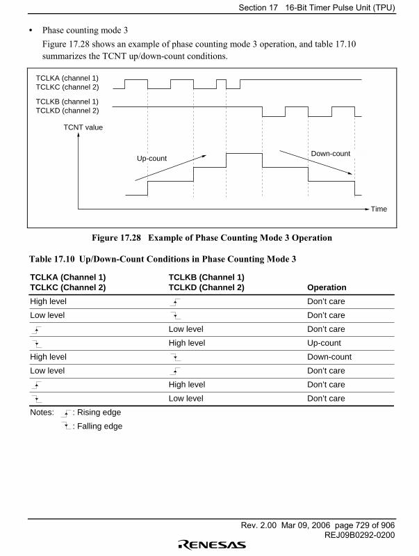
Section 17 16-Bit Timer Pulse Unit (TPU)
Rev. 2.00 Mar 09, 2006 page 729 of 906REJ09B0292-0200
• Phase counting mode 3Figure 17.28 shows an example of phase counting mode 3 operation, and table 17.10summarizes the TCNT up/down-count conditions.
TCNT value
Time
Up-count
TCLKA (channel 1)TCLKC (channel 2)
TCLKB (channel 1)TCLKD (channel 2)
Down-count
Figure 17.28 Example of Phase Counting Mode 3 Operation
Table 17.10 Up/Down-Count Conditions in Phase Counting Mode 3
TCLKA (Channel 1)TCLKC (Channel 2)
High level
Low level
High level
Low level
Notes: : Rising edge
: Falling edge
TCLKB (Channel 1)TCLKD (Channel 2)
Low level
High level
High level
Low level
Operation
Don’t care
Don’t care
Don’t care
Up-count
Down-count
Don’t care
Don’t care
Don’t care
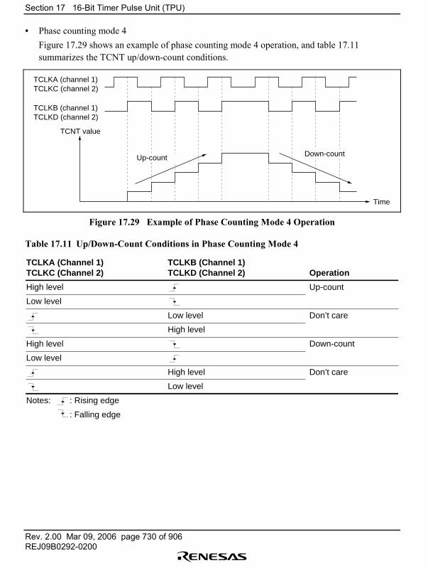
Section 17 16-Bit Timer Pulse Unit (TPU)
Rev. 2.00 Mar 09, 2006 page 730 of 906REJ09B0292-0200
• Phase counting mode 4Figure 17.29 shows an example of phase counting mode 4 operation, and table 17.11summarizes the TCNT up/down-count conditions.
Time
TCLKA (channel 1)TCLKC (channel 2)
TCLKB (channel 1)TCLKD (channel 2)
Up-count Down-count
TCNT value
Figure 17.29 Example of Phase Counting Mode 4 Operation
Table 17.11 Up/Down-Count Conditions in Phase Counting Mode 4
TCLKA (Channel 1)TCLKC (Channel 2)
High level
Low level
High level
Low level
Notes: : Rising edge
: Falling edge
TCLKB (Channel 1)TCLKD (Channel 2)
Low level
High level
High level
Low level
Operation
Up-count
Don’t care
Down-count
Don’t care
Section 17 16-Bit Timer Pulse Unit (TPU)
Rev. 2.00 Mar 09, 2006 page 731 of 906REJ09B0292-0200
17.5 Interrupts
17.5.1 Interrupt Sources and Priorities
There are three kinds of TPU interrupt source: TGR input capture/compare match, TCNToverflow, and TCNT underflow. Each interrupt source has its own status flag and enable/disabledbit, allowing generation of interrupt request signals to be enabled or disabled individually.
When an interrupt request is generated, the corresponding status flag in TSR is set to 1. If thecorresponding enable/disable bit in TIER is set to 1 at this time, an interrupt is requested. Theinterrupt request is cleared by clearing the status flag to 0.
Relative channel priorities can be changed by the interrupt controller, but the priority order withina channel is fixed. For details, see section 5, Interrupt Controller (INTC).
Table 17.12 lists the TPU interrupt sources.
Table 17.12 TPU Interrupts
ChannelInterruptSource Description
DMACActivation Priority
0 TGI0A TGR0A input capture/compare match Possible High
TGI0B TGR0B input capture/compare match Possible ↑
TGI0C TGR0C input capture/compare match Possible
TGI0D TGR0D input capture/compare match Possible
TCI0V TCNT0 overflow Not possible
1 TGI1A TGR1A input capture/compare match Not possible
TGI1B TGR1B input capture/compare match Not possible
TCI1V TCNT1 overflow Not possible
TCI1U TCNT1 underflow Not possible
2 TGI2A TGR2A input capture/compare match Not possible
TGI2B TGR2B input capture/compare match Not possible
TCI2V TCNT2 overflow Not possible ↓
TCI2U TCNT2 underflow Not possible LowNote: This table shows the initial state immediately after a reset. The relative channel priorities
can be changed by the interrupt controller.
Section 17 16-Bit Timer Pulse Unit (TPU)
Rev. 2.00 Mar 09, 2006 page 732 of 906REJ09B0292-0200
Input Capture/Compare Match Interrupt: An interrupt is requested if the TGIE bit in TIER isset to 1 when the TGF flag in TSR is set to 1 by the occurrence of a TGR input capture/comparematch on a particular channel. The interrupt request is cleared by clearing the TGF flag to 0. TheTPU has 8 input capture/compare match interrupts, four for channel 0, and two each for channels1, and 2.
Overflow Interrupt: An interrupt is requested if the TCIEV bit in TIER is set to 1 when theTCFV flag in TSR is set to 1 by the occurrence of TCNT overflow on a particular channel. Theinterrupt request is cleared by clearing the TCFV flag to 0. The TPU has three overflow interrupts,one for each channel.
Underflow Interrupt: An interrupt is requested if the TCIEU bit in TIER is set to 1 when theTCFU flag in TSR is set to 1 by the occurrence of TCNT underflow on channel. The interruptrequest is cleared by clearing the TCFU flag to 0. The TPU has two underflow interrupts, one eachfor channels 1 and 2.
17.5.2 DMAC Activation
The DMAC can be activated by the TGR input capture/compare match interrupt for a channel. Fordetails, see section 11, Direct Memory Access Controller (DMAC).
A total of four TPU input capture/compare match interrupts can be used as DMAC activationsources for channel 0.
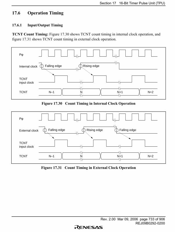
Section 17 16-Bit Timer Pulse Unit (TPU)
Rev. 2.00 Mar 09, 2006 page 733 of 906REJ09B0292-0200
17.6 Operation Timing
17.6.1 Input/Output Timing
TCNT Count Timing: Figure 17.30 shows TCNT count timing in internal clock operation, andfigure 17.31 shows TCNT count timing in external clock operation.
TCNT
TCNTinput clock
Internal clock
Pφ
N–1 N N+1 N+2
Falling edge Rising edge
Figure 17.30 Count Timing in Internal Clock Operation
TCNT
TCNTinput clock
External clock
Pφ
N–1 N N+1 N+2
Rising edge Falling edgeFalling edge
Figure 17.31 Count Timing in External Clock Operation
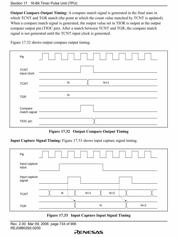
Section 17 16-Bit Timer Pulse Unit (TPU)
Rev. 2.00 Mar 09, 2006 page 734 of 906REJ09B0292-0200
Output Compare Output Timing: A compare match signal is generated in the final state inwhich TCNT and TGR match (the point at which the count value matched by TCNT is updated).When a compare match signal is generated, the output value set in TIOR is output at the outputcompare output pin (TIOC pin). After a match between TCNT and TGR, the compare matchsignal is not generated until the TCNT input clock is generated.
Figure 17.32 shows output compare output timing.
TGR
TCNT
TCNTinput clock
Pφ
N
N N+1
Comparematch signal
TIOC pin
Figure 17.32 Output Compare Output Timing
Input Capture Signal Timing: Figure 17.33 shows input capture signal timing.
TCNT
Input captureinput
Pφ
N N+1 N+2
N N+2TGR
Input capturesignal
Figure 17.33 Input Capture Input Signal Timing
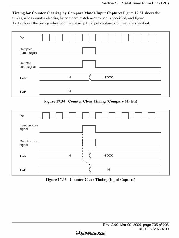
Section 17 16-Bit Timer Pulse Unit (TPU)
Rev. 2.00 Mar 09, 2006 page 735 of 906REJ09B0292-0200
Timing for Counter Clearing by Compare Match/Input Capture: Figure 17.34 shows thetiming when counter clearing by compare match occurrence is specified, and figure17.35 shows the timing when counter clearing by input capture occurrence is specified.
TCNT
Counterclear signal
Comparematch signal
Pφ
TGR N
N H'0000
Figure 17.34 Counter Clear Timing (Compare Match)
TCNT
Counter clearsignal
Input capturesignal
Pφ
TGR
N H'0000
N
Figure 17.35 Counter Clear Timing (Input Capture)

Section 17 16-Bit Timer Pulse Unit (TPU)
Rev. 2.00 Mar 09, 2006 page 736 of 906REJ09B0292-0200
Buffer Operation Timing: Figures 17.36 and 17.37 show the timing in buffer operation.
TGRA,TGRB
Comparematch signal
TCNT
Pφ
TGRC,TGRD
n N
N
n n+1
Figure 17.36 Buffer Operation Timing (Compare Match)
TGRA,TGRB
TCNT
Input capturesignal
Pφ
TGRC,TGRD
N
n
n N+1
N
N N+1
Figure 17.37 Buffer Operation Timing (Input Capture)

Section 17 16-Bit Timer Pulse Unit (TPU)
Rev. 2.00 Mar 09, 2006 page 737 of 906REJ09B0292-0200
17.6.2 Interrupt Signal Timing
TGF Flag Setting Timing in Case of Compare Match: Figure 17.38 shows the timing forsetting of the TGF flag in TSR by compare match occurrence, and TGI interrupt request signaltiming.
TGR
TCNT
TCNT inputclock
Pφ
N
N N+1
Comparematch signal
TGF flag
TGI interrupt
Figure 17.38 TGI Interrupt Timing (Compare Match)

Section 17 16-Bit Timer Pulse Unit (TPU)
Rev. 2.00 Mar 09, 2006 page 738 of 906REJ09B0292-0200
TGF Flag Setting Timing in Case of Input Capture: Figure 17.39 shows the timing for settingof the TGF flag in TSR by input capture occurrence, and TGI interrupt request signal timing.
TGR
TCNT
Input capturesignal
Pφ
N
N
TGF flag
TGI interrupt
Figure 17.39 TGI Interrupt Timing (Input Capture)
TCFV Flag/TCFU Flag Setting Timing: Figure 17.40 shows the timing for setting of the TCFVflag in TSR by overflow occurrence, and TCIV interrupt request signal timing.
Figure 17.41 shows the timing for setting of the TCFU flag in TSR by underflow occurrence, andTCIU interrupt request signal timing.
Overflowsignal
TCNT(overflow)
TCNT inputclock
Pφ
H'FFFF H'0000
TCFV flag
TCIV interrupt
Figure 17.40 TCIV Interrupt Setting Timing
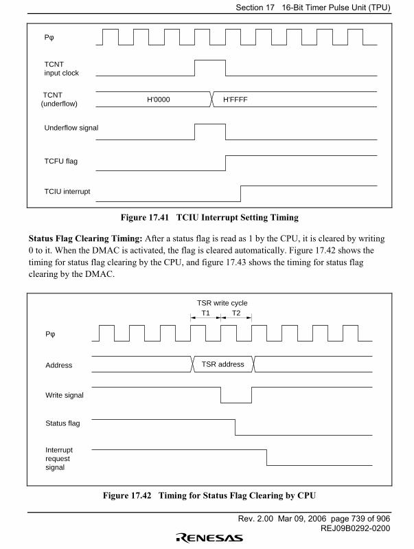
Section 17 16-Bit Timer Pulse Unit (TPU)
Rev. 2.00 Mar 09, 2006 page 739 of 906REJ09B0292-0200
Underflow signal
TCNT(underflow)
TCNTinput clock
Pφ
H'0000 H'FFFF
TCFU flag
TCIU interrupt
Figure 17.41 TCIU Interrupt Setting Timing
Status Flag Clearing Timing: After a status flag is read as 1 by the CPU, it is cleared by writing0 to it. When the DMAC is activated, the flag is cleared automatically. Figure 17.42 shows thetiming for status flag clearing by the CPU, and figure 17.43 shows the timing for status flagclearing by the DMAC.
Status flag
Write signal
Address
Pφ
TSR address
Interruptrequestsignal
TSR write cycleT1 T2
Figure 17.42 Timing for Status Flag Clearing by CPU
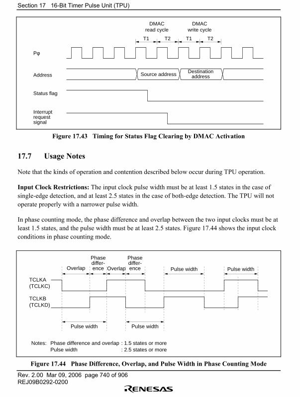
Section 17 16-Bit Timer Pulse Unit (TPU)
Rev. 2.00 Mar 09, 2006 page 740 of 906REJ09B0292-0200
Interruptrequestsignal
Status flag
Address
Pφ
Source address
DMACread cycle
T1 T2
Destinationaddress
T1 T2
DMACwrite cycle
Figure 17.43 Timing for Status Flag Clearing by DMAC Activation
17.7 Usage Notes
Note that the kinds of operation and contention described below occur during TPU operation.
Input Clock Restrictions: The input clock pulse width must be at least 1.5 states in the case ofsingle-edge detection, and at least 2.5 states in the case of both-edge detection. The TPU will notoperate properly with a narrower pulse width.
In phase counting mode, the phase difference and overlap between the two input clocks must be atleast 1.5 states, and the pulse width must be at least 2.5 states. Figure 17.44 shows the input clockconditions in phase counting mode.
Overlap
Phasediffer-ence
Phasediffer-enceOverlap
TCLKA(TCLKC)
TCLKB(TCLKD)
Pulse width Pulse width
Pulse width Pulse width
Notes: Phase difference and overlap : 1.5 states or more Pulse width : 2.5 states or more
Figure 17.44 Phase Difference, Overlap, and Pulse Width in Phase Counting Mode
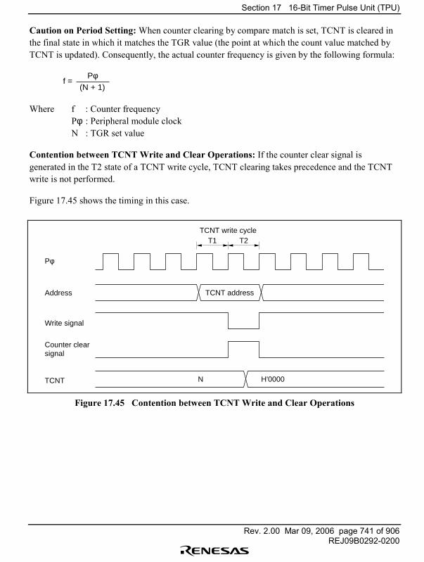
Section 17 16-Bit Timer Pulse Unit (TPU)
Rev. 2.00 Mar 09, 2006 page 741 of 906REJ09B0292-0200
Caution on Period Setting: When counter clearing by compare match is set, TCNT is cleared inthe final state in which it matches the TGR value (the point at which the count value matched byTCNT is updated). Consequently, the actual counter frequency is given by the following formula:
f =Pφ
(N + 1)
Where f : Counter frequencyPφ : Peripheral module clockN : TGR set value
Contention between TCNT Write and Clear Operations: If the counter clear signal isgenerated in the T2 state of a TCNT write cycle, TCNT clearing takes precedence and the TCNTwrite is not performed.
Figure 17.45 shows the timing in this case.
Counter clearsignal
Write signal
Address
Pφ
TCNT address
TCNT
TCNT write cycleT1 T2
N H'0000
Figure 17.45 Contention between TCNT Write and Clear Operations

Section 17 16-Bit Timer Pulse Unit (TPU)
Rev. 2.00 Mar 09, 2006 page 742 of 906REJ09B0292-0200
Contention between TCNT Write and Increment Operations: If incrementing occurs in the T2state of a TCNT write cycle, the TCNT write takes precedence and TCNT is not incremented.
Figure 17.46 shows the timing in this case.
TCNT inputclock
Write signal
Address
Pφ
TCNT address
TCNT
TCNT write cycleT1 T2
N M
TCNT write data
Figure 17.46 Contention between TCNT Write and Increment Operations

Section 17 16-Bit Timer Pulse Unit (TPU)
Rev. 2.00 Mar 09, 2006 page 743 of 906REJ09B0292-0200
Contention between TGR Write and Compare Match: If a compare match occurs in the T2state of a TGR write cycle, the TGR write takes precedence and the compare match signal isinhibited. A compare match does not occur even if the same value as before is written.
Figure 17.47 shows the timing in this case.
Comparematch signal
Write signal
Address
Pφ
TGR address
TCNT
TGR write cycleT1 T2
N M
TGR write data
TGR
N N+1
Inhibited
Figure 17.47 Contention between TGR Write and Compare Match
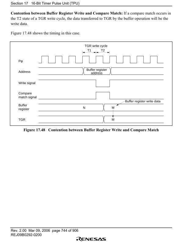
Section 17 16-Bit Timer Pulse Unit (TPU)
Rev. 2.00 Mar 09, 2006 page 744 of 906REJ09B0292-0200
Contention between Buffer Register Write and Compare Match: If a compare match occurs inthe T2 state of a TGR write cycle, the data transferred to TGR by the buffer operation will be thewrite data.
Figure 17.48 shows the timing in this case.
Comparematch signal
Write signal
Address
Pφ
Buffer registeraddress
Bufferregister
TGR write cycleT1 T2
MTGR
N M
Buffer register write data
Figure 17.48 Contention between Buffer Register Write and Compare Match
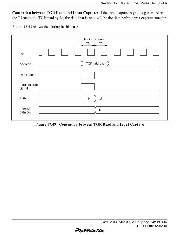
Section 17 16-Bit Timer Pulse Unit (TPU)
Rev. 2.00 Mar 09, 2006 page 745 of 906REJ09B0292-0200
Contention between TGR Read and Input Capture: If the input capture signal is generated inthe T1 state of a TGR read cycle, the data that is read will be the data before input capture transfer.
Figure 17.49 shows the timing in this case.
Input capturesignal
Read signal
Address
Pφ
TGR address
TGR
TGR read cycleT1 T2
NInternaldata bus
N M
Figure 17.49 Contention between TGR Read and Input Capture

Section 17 16-Bit Timer Pulse Unit (TPU)
Rev. 2.00 Mar 09, 2006 page 746 of 906REJ09B0292-0200
Contention between TGR Write and Input Capture: If the input capture signal is generated inthe T2 state of a TGR write cycle, the input capture operation takes precedence and the write toTGR is not performed.
Figure 17.50 shows the timing in this case.
Input capturesignal
Write signal
Address
Pφ
TCNT
TGR write cycleT1 T2
MTGR
M
TGR address
Figure 17.50 Contention between TGR Write and Input Capture
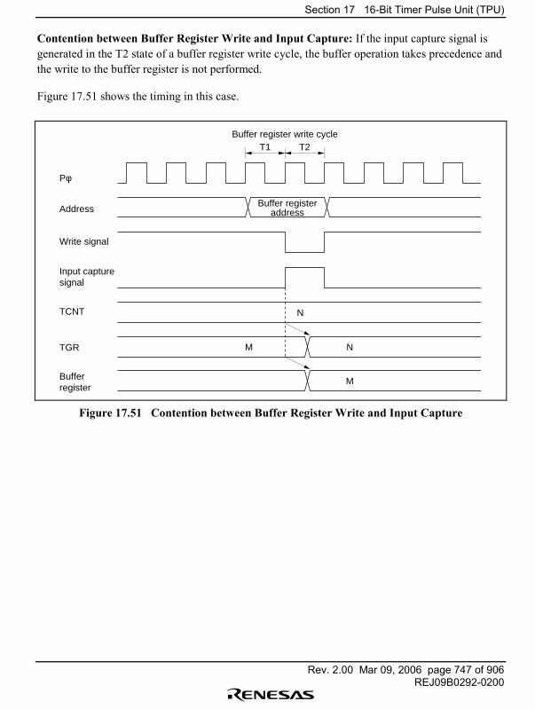
Section 17 16-Bit Timer Pulse Unit (TPU)
Rev. 2.00 Mar 09, 2006 page 747 of 906REJ09B0292-0200
Contention between Buffer Register Write and Input Capture: If the input capture signal isgenerated in the T2 state of a buffer register write cycle, the buffer operation takes precedence andthe write to the buffer register is not performed.
Figure 17.51 shows the timing in this case.
Input capturesignal
Write signal
Address
Pφ
TCNT
Buffer register write cycleT1 T2
NTGR
N
M
MBufferregister
Buffer registeraddress
Figure 17.51 Contention between Buffer Register Write and Input Capture
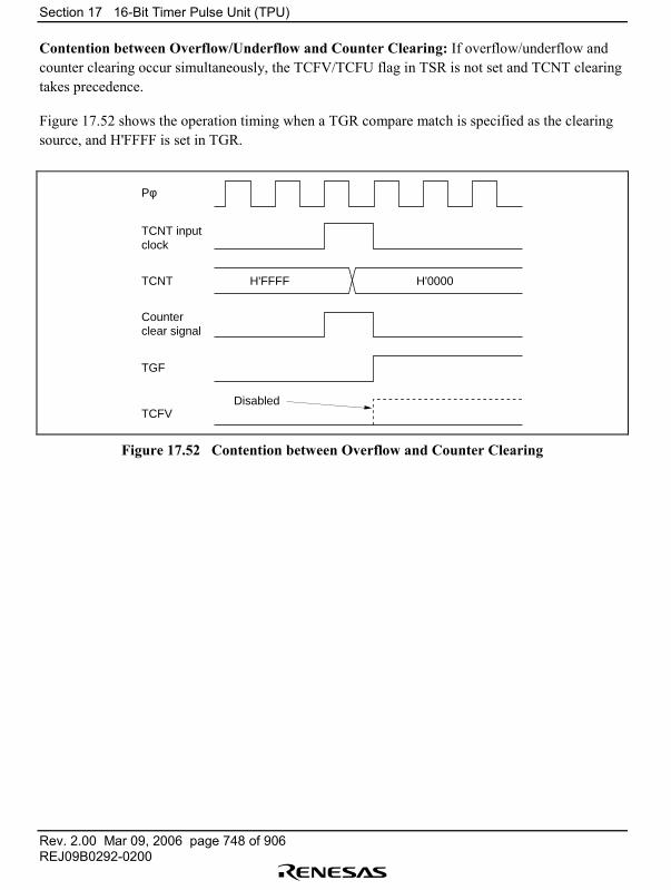
Section 17 16-Bit Timer Pulse Unit (TPU)
Rev. 2.00 Mar 09, 2006 page 748 of 906REJ09B0292-0200
Contention between Overflow/Underflow and Counter Clearing: If overflow/underflow andcounter clearing occur simultaneously, the TCFV/TCFU flag in TSR is not set and TCNT clearingtakes precedence.
Figure 17.52 shows the operation timing when a TGR compare match is specified as the clearingsource, and H'FFFF is set in TGR.
Counterclear signal
TCNT input clock
Pφ
TCNT
TGF
DisabledTCFV
H'FFFF H'0000
Figure 17.52 Contention between Overflow and Counter Clearing
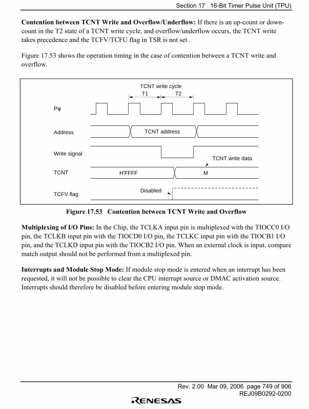
Section 17 16-Bit Timer Pulse Unit (TPU)
Rev. 2.00 Mar 09, 2006 page 749 of 906REJ09B0292-0200
Contention between TCNT Write and Overflow/Underflow: If there is an up-count or down-count in the T2 state of a TCNT write cycle, and overflow/underflow occurs, the TCNT writetakes precedence and the TCFV/TCFU flag in TSR is not set .
Figure 17.53 shows the operation timing in the case of contention between a TCNT write andoverflow.
Write signal
Address
Pφ
TCNT address
TCNT
TCNT write cycleT1 T2
H'FFFF M
TCNT write data
TCFV flagDisabled
Figure 17.53 Contention between TCNT Write and Overflow
Multiplexing of I/O Pins: In the Chip, the TCLKA input pin is multiplexed with the TIOCC0 I/Opin, the TCLKB input pin with the TIOCD0 I/O pin, the TCLKC input pin with the TIOCB1 I/Opin, and the TCLKD input pin with the TIOCB2 I/O pin. When an external clock is input, comparematch output should not be performed from a multiplexed pin.
Interrupts and Module Stop Mode: If module stop mode is entered when an interrupt has beenrequested, it will not be possible to clear the CPU interrupt source or DMAC activation source.Interrupts should therefore be disabled before entering module stop mode.
Section 17 16-Bit Timer Pulse Unit (TPU)
Rev. 2.00 Mar 09, 2006 page 750 of 906REJ09B0292-0200
17.8 Usage Notes
17.8.1 Clearing Flags in TSR0 to TSR2
When bits TCFV, TGFD, TGFC, TGFB, and TGFA in TSR0, and bits TCFU, TCFV, TGFB, andTGFA in TSR1 and TSR2, are cleared, it may happen that the interrupt request in the internallogic cannot be cleared although the flag is cleared. In this case, if interrupt acceptance is enabled,another interrupt will be generated.
Either of the following measures should therefore be taken when clearing flags in TSR0 to TSR2.
1. Execute clearing while the TPU timer is counting up.2. If clearing when the TPU timer is stopped, write 0 to the flag again after executing clearing.
17.8.2 DMA Transfer by TPU0
When DMA transfer is performed by means of TPU channel 0 compare match or input capture,internal logic interrupt requests (transfer requests) may not be cleared correctly. Therefore, it maynot be possible to execute DMA transfer when a subsequent transfer request is generated by TPUchannel 0 compare match or input capture.
Either of the following measures should therefore be taken when performing DMA transfer bymeans of TPU channel 0 compare match or input capture.
1. Do not set on-chip RAM as the DMA transfer source or destination.2. When on-chip RAM has not been set as the DMA transfer source or destination, execute the
transfer while the TPU channel 0 timer is counting up.
Section 18 User Debug Interface (H-UDI)
Rev. 2.00 Mar 09, 2006 page 751 of 906REJ09B0292-0200
Section 18 User Debug Interface (H-UDI)
18.1 Overview
The user debug interface (H-UDI) provides data transfer and interrupt request functions. The H-UDI performs serial transfer by means of external signal control.
18.1.1 Features
The H-UDI has the following features conforming to the IEEE 1149.1 standard.
• Five test signals (TCK, TDI, TDO, TMS, and TRST)• TAP controller• Instruction register• Data register• Bypass register• Boundary scan register
The H-UDI has seven instructions.
• Bypass modeTest mode conforming to IEEE 1149.1
• EXTEST modeTest mode corresponding to IEEE1149.1.
• SAMPLE/PRELOAD modeTest mode corresponding to IEEE1149.1.
• CLAMP modeTest mode corresponding to IEEE1149.1.
• HIGHZ modeTest mode corresponding to IEEE1149.1.
• IDCODE modeTest mode corresponding to IEEE1149.1.
• H-UDI interruptH-UDI interrupt request to INTC
This chip does not support test modes other than bypass mode.
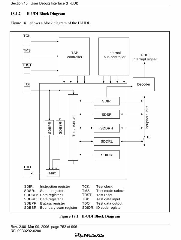
Section 18 User Debug Interface (H-UDI)
Rev. 2.00 Mar 09, 2006 page 752 of 906REJ09B0292-0200
18.1.2 H-UDI Block Diagram
Figure 18.1 shows a block diagram of the H-UDI.
TCK
TMS
TRST
TDI
TAPcontroller
Internalbus controller
H-UDIinterrupt signal
SDSR
SDIDR
SDDRH
SDDRL
Sh
ift r
eg
iste
r
SD
BP
R
Mux
TDO
Pe
rip
he
ral b
us
SDIR: Instruction register TCK: Test clockSDSR: Status register TMS: Test mode selectSDDRH: Data register H TRST: Test resetSDDRL: Data register L TDI: Test data inputSDBPR: Bypass register TDO: Test data outputSDBSR: Boundary scan register SDIDR: ID code register
Decoder
16
SDIR
SD
BS
R
Figure 18.1 H-UDI Block Diagram
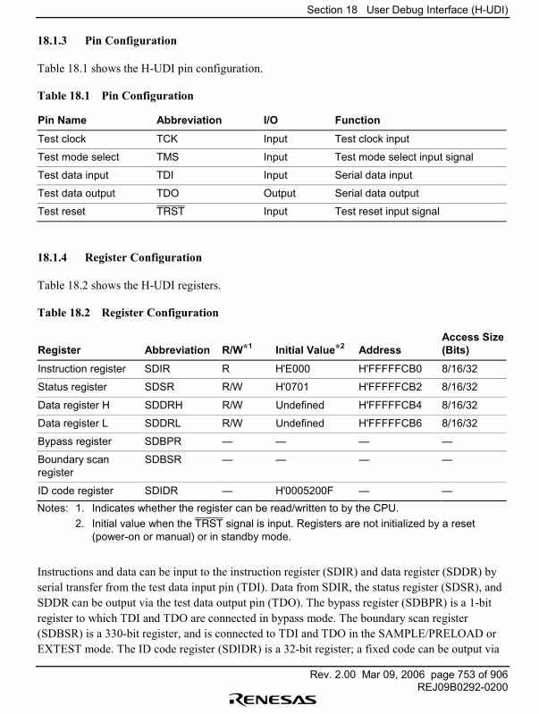
Section 18 User Debug Interface (H-UDI)
Rev. 2.00 Mar 09, 2006 page 753 of 906REJ09B0292-0200
18.1.3 Pin Configuration
Table 18.1 shows the H-UDI pin configuration.
Table 18.1 Pin Configuration
Pin Name Abbreviation I/O Function
Test clock TCK Input Test clock input
Test mode select TMS Input Test mode select input signal
Test data input TDI Input Serial data input
Test data output TDO Output Serial data output
Test reset TRST Input Test reset input signal
18.1.4 Register Configuration
Table 18.2 shows the H-UDI registers.
Table 18.2 Register Configuration
Register Abbreviation R/W*1 Initial Value*2 AddressAccess Size(Bits)
Instruction register SDIR R H'E000 H'FFFFFCB0 8/16/32
Status register SDSR R/W H'0701 H'FFFFFCB2 8/16/32
Data register H SDDRH R/W Undefined H'FFFFFCB4 8/16/32
Data register L SDDRL R/W Undefined H'FFFFFCB6 8/16/32
Bypass register SDBPR � � � �
Boundary scanregister
SDBSR � � � �
ID code register SDIDR � H'0005200F � �Notes: 1. Indicates whether the register can be read/written to by the CPU.
2. Initial value when the TRST signal is input. Registers are not initialized by a reset(power-on or manual) or in standby mode.
Instructions and data can be input to the instruction register (SDIR) and data register (SDDR) byserial transfer from the test data input pin (TDI). Data from SDIR, the status register (SDSR), andSDDR can be output via the test data output pin (TDO). The bypass register (SDBPR) is a 1-bitregister to which TDI and TDO are connected in bypass mode. The boundary scan register(SDBSR) is a 330-bit register, and is connected to TDI and TDO in the SAMPLE/PRELOAD orEXTEST mode. The ID code register (SDIDR) is a 32-bit register; a fixed code can be output via
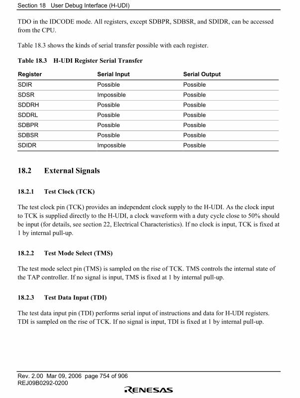
Section 18 User Debug Interface (H-UDI)
Rev. 2.00 Mar 09, 2006 page 754 of 906REJ09B0292-0200
TDO in the IDCODE mode. All registers, except SDBPR, SDBSR, and SDIDR, can be accessedfrom the CPU.
Table 18.3 shows the kinds of serial transfer possible with each register.
Table 18.3 H-UDI Register Serial Transfer
Register Serial Input Serial Output
SDIR Possible Possible
SDSR Impossible Possible
SDDRH Possible Possible
SDDRL Possible Possible
SDBPR Possible Possible
SDBSR Possible Possible
SDIDR Impossible Possible
18.2 External Signals
18.2.1 Test Clock (TCK)
The test clock pin (TCK) provides an independent clock supply to the H-UDI. As the clock inputto TCK is supplied directly to the H-UDI, a clock waveform with a duty cycle close to 50% shouldbe input (for details, see section 22, Electrical Characteristics). If no clock is input, TCK is fixed at1 by internal pull-up.
18.2.2 Test Mode Select (TMS)
The test mode select pin (TMS) is sampled on the rise of TCK. TMS controls the internal state ofthe TAP controller. If no signal is input, TMS is fixed at 1 by internal pull-up.
18.2.3 Test Data Input (TDI)
The test data input pin (TDI) performs serial input of instructions and data for H-UDI registers.TDI is sampled on the rise of TCK. If no signal is input, TDI is fixed at 1 by internal pull-up.
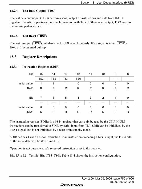
Section 18 User Debug Interface (H-UDI)
Rev. 2.00 Mar 09, 2006 page 755 of 906REJ09B0292-0200
18.2.4 Test Data Output (TDO)
The test data output pin (TDO) performs serial output of instructions and data from H-UDIregisters. Transfer is performed in synchronization with TCK. If there is no output, TDO goes tothe high-impedance state.
18.2.5 Test Reset (TRSTTRSTTRSTTRST)
The test reset pin (TRST) initializes the H-UDI asynchronously. If no signal is input, TRST isfixed at 1 by internal pull-up.
18.3 Register Descriptions
18.3.1 Instruction Register (SDIR)
Bit: 15 14 13 12 11 10 9 8
TS3 TS2 TS1 TS0 � � � �
Initial value: 1 1 1 0 0 0 0 0
R/W: R R R R R R R R
Bit: 7 6 5 4 3 2 1 0
� � � � � � � �
Initial value: 0 0 0 0 0 0 0 0
R/W: R R R R R R R R
The instruction register (SDIR) is a 16-bit register that can only be read by the CPU. H-UDIinstructions can be transferred to SDIR by serial input from TDI. SDIR can be initialized by theTRST signal, but is not initialized by a reset or in standby mode.
SDIR defines 4 valid bits for instruction. If an instruction exceeding 4 bits is input, the last 4 bitsof the serial data will be stored in SDIR.
Operation is not guaranteed if a reserved instruction is set in this register.
Bits 15 to 12�Test Set Bits (TS3�TS0): Table 18.4 shows the instruction configuration.
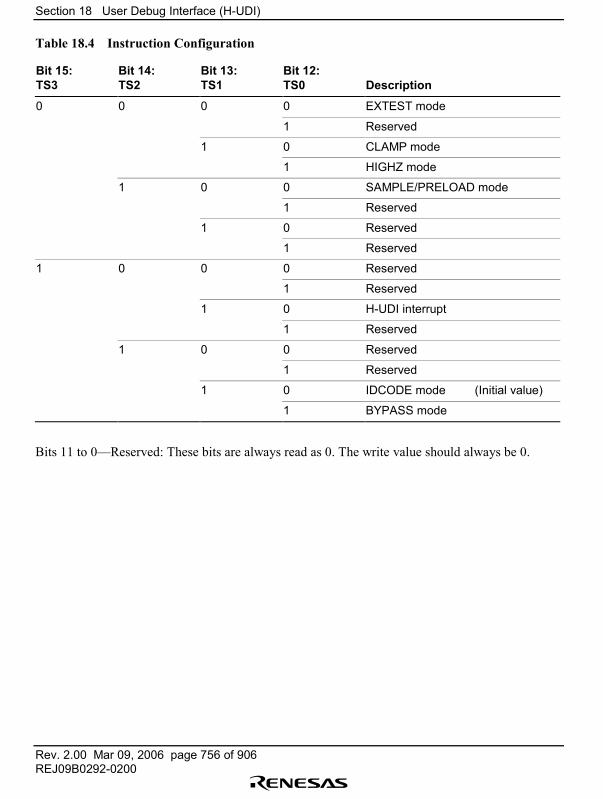
Section 18 User Debug Interface (H-UDI)
Rev. 2.00 Mar 09, 2006 page 756 of 906REJ09B0292-0200
Table 18.4 Instruction Configuration
Bit 15:TS3
Bit 14:TS2
Bit 13:TS1
Bit 12:TS0 Description
0 0 0 0 EXTEST mode
1 Reserved
1 0 CLAMP mode
1 HIGHZ mode
1 0 0 SAMPLE/PRELOAD mode
1 Reserved
1 0 Reserved
1 Reserved
1 0 0 0 Reserved
1 Reserved
1 0 H-UDI interrupt
1 Reserved
1 0 0 Reserved
1 Reserved
1 0 IDCODE mode (Initial value)
1 BYPASS mode
Bits 11 to 0�Reserved: These bits are always read as 0. The write value should always be 0.
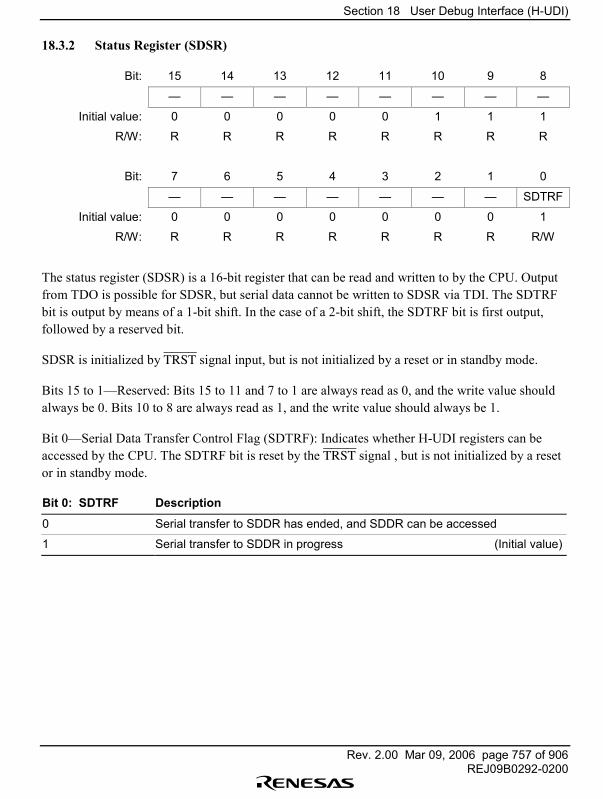
Section 18 User Debug Interface (H-UDI)
Rev. 2.00 Mar 09, 2006 page 757 of 906REJ09B0292-0200
18.3.2 Status Register (SDSR)
Bit: 15 14 13 12 11 10 9 8
� � � � � � � �
Initial value: 0 0 0 0 0 1 1 1
R/W: R R R R R R R R
Bit: 7 6 5 4 3 2 1 0
� � � � � � � SDTRF
Initial value: 0 0 0 0 0 0 0 1
R/W: R R R R R R R R/W
The status register (SDSR) is a 16-bit register that can be read and written to by the CPU. Outputfrom TDO is possible for SDSR, but serial data cannot be written to SDSR via TDI. The SDTRFbit is output by means of a 1-bit shift. In the case of a 2-bit shift, the SDTRF bit is first output,followed by a reserved bit.
SDSR is initialized by TRST signal input, but is not initialized by a reset or in standby mode.
Bits 15 to 1�Reserved: Bits 15 to 11 and 7 to 1 are always read as 0, and the write value shouldalways be 0. Bits 10 to 8 are always read as 1, and the write value should always be 1.
Bit 0�Serial Data Transfer Control Flag (SDTRF): Indicates whether H-UDI registers can beaccessed by the CPU. The SDTRF bit is reset by the TRST signal , but is not initialized by a resetor in standby mode.
Bit 0: SDTRF Description
0 Serial transfer to SDDR has ended, and SDDR can be accessed
1 Serial transfer to SDDR in progress (Initial value)
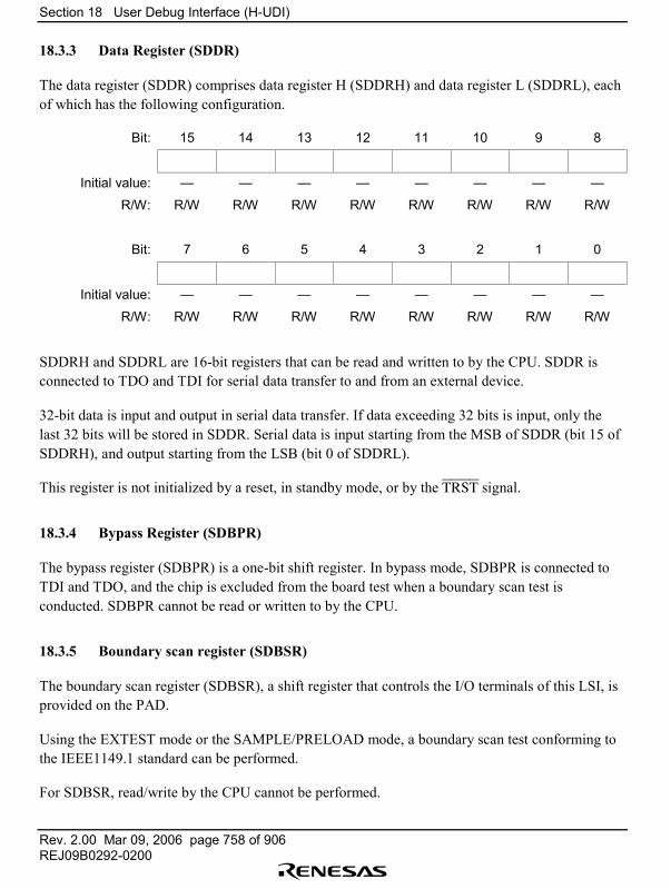
Section 18 User Debug Interface (H-UDI)
Rev. 2.00 Mar 09, 2006 page 758 of 906REJ09B0292-0200
18.3.3 Data Register (SDDR)
The data register (SDDR) comprises data register H (SDDRH) and data register L (SDDRL), eachof which has the following configuration.
Bit: 15 14 13 12 11 10 9 8
Initial value: � � � � � � � �
R/W: R/W R/W R/W R/W R/W R/W R/W R/W
Bit: 7 6 5 4 3 2 1 0
Initial value: � � � � � � � �
R/W: R/W R/W R/W R/W R/W R/W R/W R/W
SDDRH and SDDRL are 16-bit registers that can be read and written to by the CPU. SDDR isconnected to TDO and TDI for serial data transfer to and from an external device.
32-bit data is input and output in serial data transfer. If data exceeding 32 bits is input, only thelast 32 bits will be stored in SDDR. Serial data is input starting from the MSB of SDDR (bit 15 ofSDDRH), and output starting from the LSB (bit 0 of SDDRL).
This register is not initialized by a reset, in standby mode, or by the TRST signal.
18.3.4 Bypass Register (SDBPR)
The bypass register (SDBPR) is a one-bit shift register. In bypass mode, SDBPR is connected toTDI and TDO, and the chip is excluded from the board test when a boundary scan test isconducted. SDBPR cannot be read or written to by the CPU.
18.3.5 Boundary scan register (SDBSR)
The boundary scan register (SDBSR), a shift register that controls the I/O terminals of this LSI, isprovided on the PAD.
Using the EXTEST mode or the SAMPLE/PRELOAD mode, a boundary scan test conforming tothe IEEE1149.1 standard can be performed.
For SDBSR, read/write by the CPU cannot be performed.

Section 18 User Debug Interface (H-UDI)
Rev. 2.00 Mar 09, 2006 page 759 of 906REJ09B0292-0200
Table 18.5 shows the relationship between the terminals of the LSI and the boundary scan register.
Table 18.5 Correspondence between Pins and Boundary Scan Register Bits
Pin No. Pin Name Input/Output Bit No.from TDI34 D0 Input 329
Output 328Output enable 327
36 D1 Input 326Output 325Output enable 324
37 D2 Input 323Output 322Output enable 321
38 D3 Input 320Output 319Output enable 318
39 D4 Input 317Output 316Output enable 315
40 D5 Input 314Output 313Output enable 312
41 D6 Input 311Output 310Output enable 309
43 D7 Input 308Output 307Output enable 306
44 D8 Input 305Output 304Output enable 303
46 D9 Input 302Output 301Output enable 300

Section 18 User Debug Interface (H-UDI)
Rev. 2.00 Mar 09, 2006 page 760 of 906REJ09B0292-0200
Pin No. Pin Name Input/Output Bit No.
47 D10 Input 299
Output 298
Output enable 297
48 D11 Input 296
Output 295
Output enable 294
49 D12 Input 293
Output 292
Output enable 291
51 D13 Input 290
Output 289
Output enable 288
53 D14 Input 287
Output 286
Output enable 285
54 D15 Input 284
Output 283
Output enable 282
55 D16 Input 281
Output 280
Output enable 279
56 D17 Input 278
Output 277
Output enable 276
57 D18 Input 275
Output 274
Output enable 273
59 D19 Input 272
Output 271
Output enable 270
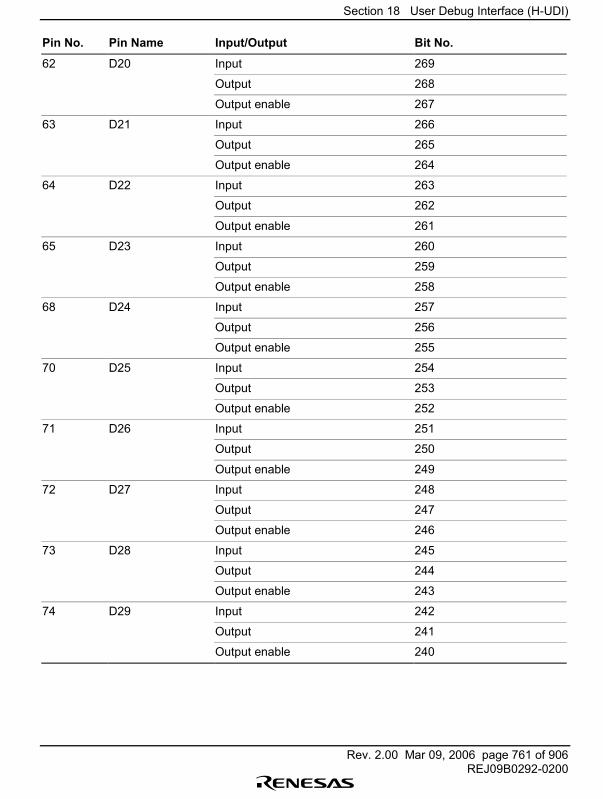
Section 18 User Debug Interface (H-UDI)
Rev. 2.00 Mar 09, 2006 page 761 of 906REJ09B0292-0200
Pin No. Pin Name Input/Output Bit No.
62 D20 Input 269
Output 268
Output enable 267
63 D21 Input 266
Output 265
Output enable 264
64 D22 Input 263
Output 262
Output enable 261
65 D23 Input 260
Output 259
Output enable 258
68 D24 Input 257
Output 256
Output enable 255
70 D25 Input 254
Output 253
Output enable 252
71 D26 Input 251
Output 250
Output enable 249
72 D27 Input 248
Output 247
Output enable 246
73 D28 Input 245
Output 244
Output enable 243
74 D29 Input 242
Output 241
Output enable 240
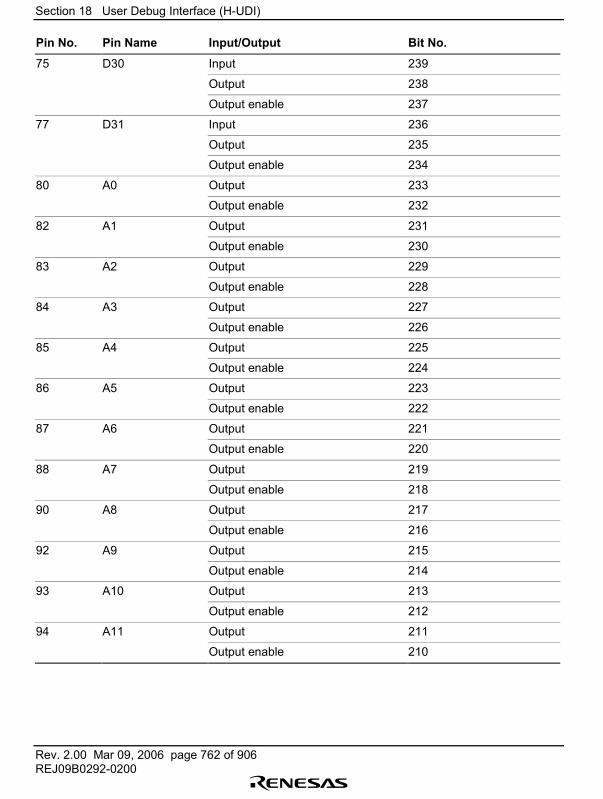
Section 18 User Debug Interface (H-UDI)
Rev. 2.00 Mar 09, 2006 page 762 of 906REJ09B0292-0200
Pin No. Pin Name Input/Output Bit No.
75 D30 Input 239
Output 238
Output enable 237
77 D31 Input 236
Output 235
Output enable 234
80 A0 Output 233
Output enable 232
82 A1 Output 231
Output enable 230
83 A2 Output 229
Output enable 228
84 A3 Output 227
Output enable 226
85 A4 Output 225
Output enable 224
86 A5 Output 223
Output enable 222
87 A6 Output 221
Output enable 220
88 A7 Output 219
Output enable 218
90 A8 Output 217
Output enable 216
92 A9 Output 215
Output enable 214
93 A10 Output 213
Output enable 212
94 A11 Output 211
Output enable 210
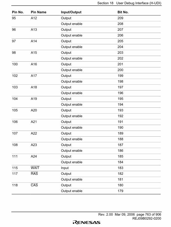
Section 18 User Debug Interface (H-UDI)
Rev. 2.00 Mar 09, 2006 page 763 of 906REJ09B0292-0200
Pin No. Pin Name Input/Output Bit No.
95 A12 Output 209
Output enable 208
96 A13 Output 207
Output enable 206
97 A14 Output 205
Output enable 204
98 A15 Output 203
Output enable 202
100 A16 Output 201
Output enable 200
102 A17 Output 199
Output enable 198
103 A18 Output 197
Output enable 196
104 A19 Output 195
Output enable 194
105 A20 Output 193
Output enable 192
106 A21 Output 191
Output enable 190
107 A22 Output 189
Output enable 188
108 A23 Output 187
Output enable 186
111 A24 Output 185
Output enable 184
115 WAIT Input 183
117 RAS Output 182
Output enable 181
118 CAS Output 180
Output enable 179
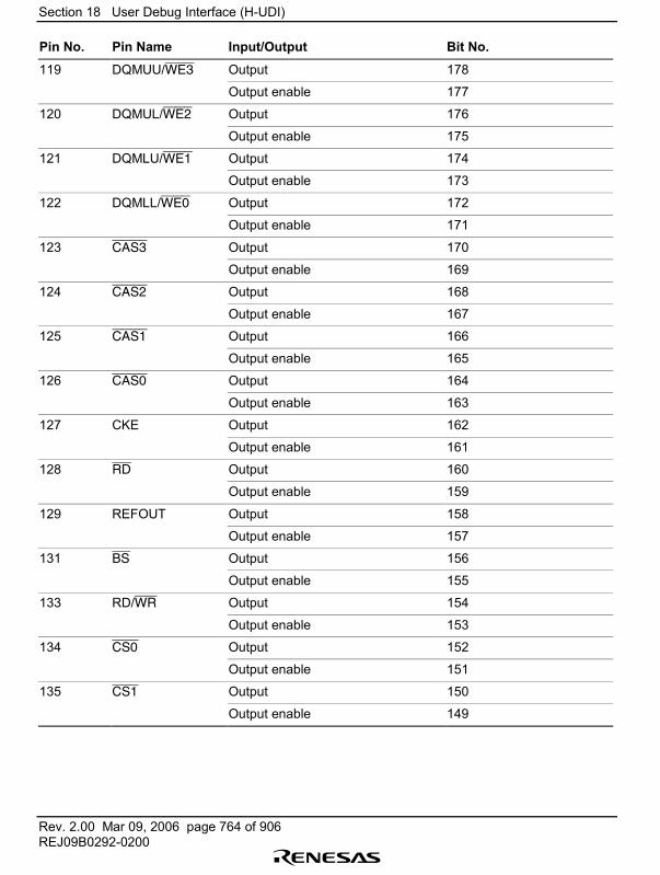
Section 18 User Debug Interface (H-UDI)
Rev. 2.00 Mar 09, 2006 page 764 of 906REJ09B0292-0200
Pin No. Pin Name Input/Output Bit No.
119 DQMUU/WE3 Output 178
Output enable 177
120 DQMUL/WE2 Output 176
Output enable 175
121 DQMLU/WE1 Output 174
Output enable 173
122 DQMLL/WE0 Output 172
Output enable 171
123 CAS3 Output 170
Output enable 169
124 CAS2 Output 168
Output enable 167
125 CAS1 Output 166
Output enable 165
126 CAS0 Output 164
Output enable 163
127 CKE Output 162
Output enable 161
128 RD Output 160
Output enable 159
129 REFOUT Output 158
Output enable 157
131 BS Output 156
Output enable 155
133 RD/WR Output 154
Output enable 153
134 CS0 Output 152
Output enable 151
135 CS1 Output 150
Output enable 149
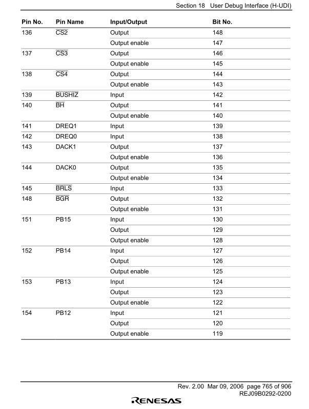
Section 18 User Debug Interface (H-UDI)
Rev. 2.00 Mar 09, 2006 page 765 of 906REJ09B0292-0200
Pin No. Pin Name Input/Output Bit No.
136 CS2 Output 148
Output enable 147
137 CS3 Output 146
Output enable 145
138 CS4 Output 144
Output enable 143
139 BUSHIZ Input 142
140 BH Output 141
Output enable 140
141 DREQ1 Input 139
142 DREQ0 Input 138
143 DACK1 Output 137
Output enable 136
144 DACK0 Output 135
Output enable 134
145 BRLS Input 133
148 BGR Output 132
Output enable 131
151 PB15 Input 130
Output 129
Output enable 128
152 PB14 Input 127
Output 126
Output enable 125
153 PB13 Input 124
Output 123
Output enable 122
154 PB12 Input 121
Output 120
Output enable 119

Section 18 User Debug Interface (H-UDI)
Rev. 2.00 Mar 09, 2006 page 766 of 906REJ09B0292-0200
Pin No. Pin Name Input/Output Bit No.
156 PB11 Input 118
Output 117
Output enable 116
158 PB10 Input 115
Output 114
Output enable 113
159 PB9 Input 112
Output 111
Output enable 110
160 PB8 Input 109
Output 108
Output enable 107
161 PB7 Input 106
Output 105
Output enable 104
162 PB6 Input 103
Output 102
Output enable 101
163 PB5 Input 100
Output 99
Output enable 98
164 PB4 Input 97
Output 96
Output enable 95
165 PB3 Input 94
Output 93
Output enable 92
166 PB2 Input 91
Output 90
Output enable 89
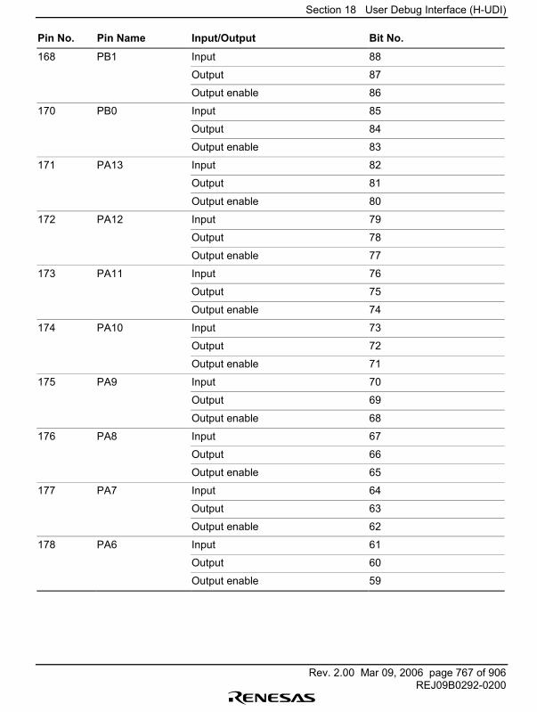
Section 18 User Debug Interface (H-UDI)
Rev. 2.00 Mar 09, 2006 page 767 of 906REJ09B0292-0200
Pin No. Pin Name Input/Output Bit No.
168 PB1 Input 88
Output 87
Output enable 86
170 PB0 Input 85
Output 84
Output enable 83
171 PA13 Input 82
Output 81
Output enable 80
172 PA12 Input 79
Output 78
Output enable 77
173 PA11 Input 76
Output 75
Output enable 74
174 PA10 Input 73
Output 72
Output enable 71
175 PA9 Input 70
Output 69
Output enable 68
176 PA8 Input 67
Output 66
Output enable 65
177 PA7 Input 64
Output 63
Output enable 62
178 PA6 Input 61
Output 60
Output enable 59
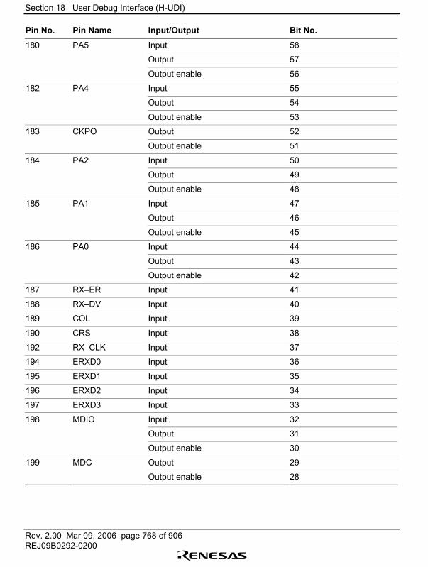
Section 18 User Debug Interface (H-UDI)
Rev. 2.00 Mar 09, 2006 page 768 of 906REJ09B0292-0200
Pin No. Pin Name Input/Output Bit No.
180 PA5 Input 58
Output 57
Output enable 56
182 PA4 Input 55
Output 54
Output enable 53
183 CKPO Output 52
Output enable 51
184 PA2 Input 50
Output 49
Output enable 48
185 PA1 Input 47
Output 46
Output enable 45
186 PA0 Input 44
Output 43
Output enable 42
187 RX�ER Input 41
188 RX�DV Input 40
189 COL Input 39
190 CRS Input 38
192 RX�CLK Input 37
194 ERXD0 Input 36
195 ERXD1 Input 35
196 ERXD2 Input 34
197 ERXD3 Input 33
198 MDIO Input 32
Output 31
Output enable 30
199 MDC Output 29
Output enable 28
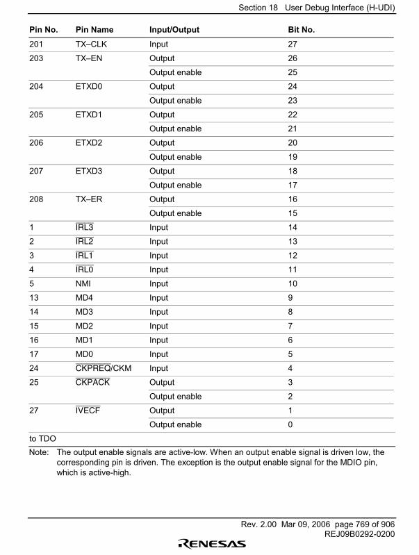
Section 18 User Debug Interface (H-UDI)
Rev. 2.00 Mar 09, 2006 page 769 of 906REJ09B0292-0200
Pin No. Pin Name Input/Output Bit No.
201 TX�CLK Input 27
203 TX�EN Output 26
Output enable 25
204 ETXD0 Output 24
Output enable 23
205 ETXD1 Output 22
Output enable 21
206 ETXD2 Output 20
Output enable 19
207 ETXD3 Output 18
Output enable 17
208 TX�ER Output 16
Output enable 15
1 IRL3 Input 14
2 IRL2 Input 13
3 IRL1 Input 12
4 IRL0 Input 11
5 NMI Input 10
13 MD4 Input 9
14 MD3 Input 8
15 MD2 Input 7
16 MD1 Input 6
17 MD0 Input 5
24 CKPREQ/CKM Input 4
25 CKPACK Output 3
Output enable 2
27 IVECF Output 1
Output enable 0
to TDONote: The output enable signals are active-low. When an output enable signal is driven low, the
corresponding pin is driven. The exception is the output enable signal for the MDIO pin,which is active-high.

Section 18 User Debug Interface (H-UDI)
Rev. 2.00 Mar 09, 2006 page 770 of 906REJ09B0292-0200
18.3.6 ID code register (SDIDR)
The ID code register (SDIDR) is a 32-bit register. In the IDCODE mode, SDIDR can outputH'0005200F, which is a fixed code, from TDO. However, no serial data can be written to SDIDRvia TDI. For SDIDR, read/write by the CPU cannot be performed.
31 28 27 12 11 1 0
0000 0001 0000 0101 0010 0000 0000 111 1
Version(4 bits)
Part Number(16 bits)
Manufacture Identify(11 bits)
Fixed Code(1 bit)
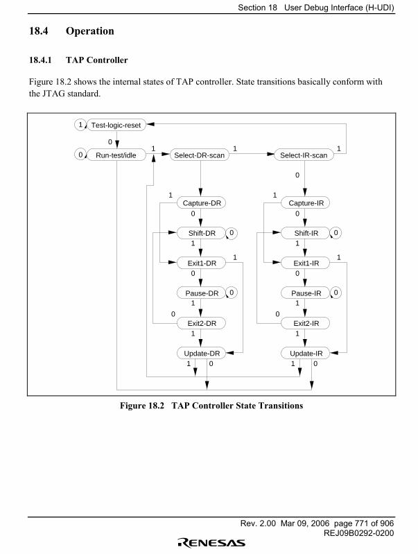
Section 18 User Debug Interface (H-UDI)
Rev. 2.00 Mar 09, 2006 page 771 of 906REJ09B0292-0200
18.4 Operation
18.4.1 TAP Controller
Figure 18.2 shows the internal states of TAP controller. State transitions basically conform withthe JTAG standard.
Test-logic-reset
Capture-DR
Shift-DR
Exit1-DR
Pause-DR
Exit2-DR
Update-DR
Select-DR-scanRun-test/idle
1
0
0
0
01 1 1
1 1
1
0
0
1
0
1
1
1 0
Capture-IR
Shift-IR
Exit1-IR
Pause-IR
Exit2-IR
Update-IR
Select-IR-scan
0
0
1
0
0
1
0
1
1
1 0
0
Figure 18.2 TAP Controller State Transitions
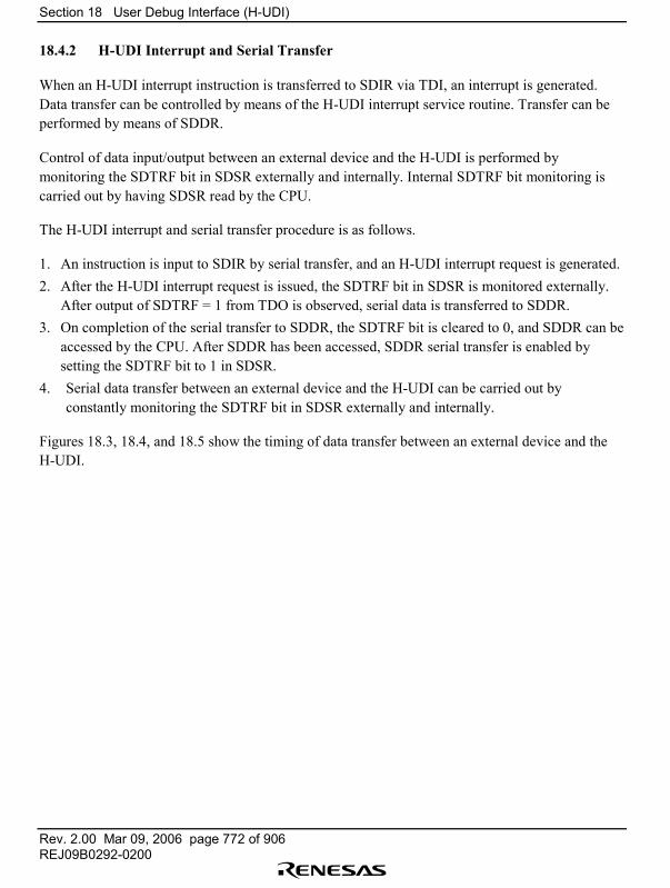
Section 18 User Debug Interface (H-UDI)
Rev. 2.00 Mar 09, 2006 page 772 of 906REJ09B0292-0200
18.4.2 H-UDI Interrupt and Serial Transfer
When an H-UDI interrupt instruction is transferred to SDIR via TDI, an interrupt is generated.Data transfer can be controlled by means of the H-UDI interrupt service routine. Transfer can beperformed by means of SDDR.
Control of data input/output between an external device and the H-UDI is performed bymonitoring the SDTRF bit in SDSR externally and internally. Internal SDTRF bit monitoring iscarried out by having SDSR read by the CPU.
The H-UDI interrupt and serial transfer procedure is as follows.
1. An instruction is input to SDIR by serial transfer, and an H-UDI interrupt request is generated.2. After the H-UDI interrupt request is issued, the SDTRF bit in SDSR is monitored externally.
After output of SDTRF = 1 from TDO is observed, serial data is transferred to SDDR.3. On completion of the serial transfer to SDDR, the SDTRF bit is cleared to 0, and SDDR can be
accessed by the CPU. After SDDR has been accessed, SDDR serial transfer is enabled bysetting the SDTRF bit to 1 in SDSR.
4. Serial data transfer between an external device and the H-UDI can be carried out byconstantly monitoring the SDTRF bit in SDSR externally and internally.
Figures 18.3, 18.4, and 18.5 show the timing of data transfer between an external device and theH-UDI.

Section 18 User Debug Interface (H-UDI)
Rev. 2.00 Mar 09, 2006 page 773 of 906REJ09B0292-0200
SDTRF1 0 1
SDSR SDDR SDSR SDDR
Shift CPU Shift CPU
Input/output
Serial data
H-UDI interrupt request
SDTRF (in SDSR)*1
SDSR and SDDR MUX*2
SDDR access state
Instruction Input
Shift disabled
Shift enabled
SDSR serial transfer(monitoring)
Shift enabled
Notes: 1. SDTRF flag (in SDSR): Indicates whether SDDR access by the CPU or serial transfer data input/output to SDDR is possible.
1 SDDR is shift-disabled. SDDR access by the CPU is enabled.
2 SDDR is shift-enabled. Do not access SDDR until SDTRF = 0.
Conditions:• SDTRF = 1 — When TRST = 0 — When the CPU writes 1 — In bypass mode• SDTRF = 0 — End of SDDR shift access in serial transfer
2. SDSR/SDDR (Update-DR state) internal MUX switchover timing • Switchover from SDSR to SDDR: On completion of serial transfer in which SDTRF = 1 is output from TDO • Switchover from SDDR to SDSR: On completion of serial transfer to SDDR
Figure 18.3 Data Input/Output Timing Chart (1)
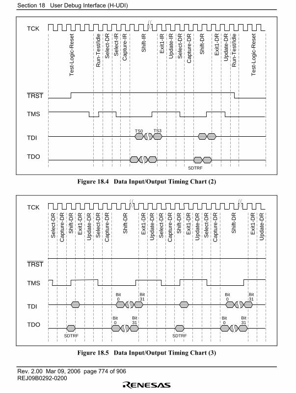
Section 18 User Debug Interface (H-UDI)
Rev. 2.00 Mar 09, 2006 page 774 of 906REJ09B0292-0200
TCK
TMS
TDI
TDO
TRST
Tes
t-Lo
gic-
Res
et
Run
-Tes
t/Idl
e
Sel
ect-
DR
Sel
ect-
IR
Cap
ture
-IR
Shi
ft-IR
Upd
ate-
IR
Sel
ect-
DR
Cap
ture
-DR
Shi
ft-D
R
Tes
t-Lo
gic-
Res
et
Run
-Tes
t/Idl
e
Exi
t1-D
R
Upd
ate-
DR
TS0 TS3
Exi
t1-I
RSDTRF
Figure 18.4 Data Input/Output Timing Chart (2)
TCK
TMS
TDI
TDO
TRST
Sel
ect-
DR
Sel
ect-
DR
Cap
ture
-DR
Shi
ft-D
R
Exi
t1-D
R
Upd
ate-
DR
Sel
ect-
DR
Cap
ture
-DR
Shi
ft-D
R
Upd
ate-
DR
Bit0
Bit31
Bit0
Bit31
Bit0
Bit31
Bit0
Bit31
SDTRF SDTRF
Shi
ft-D
R
Cap
ture
-DR
Shi
ft-D
R
Sel
ect-
DR
Upd
ate-
DR
Cap
ture
-DR
Upd
ate-
DR
Exi
t1-D
R
Exi
t1-D
R
Exi
t1-D
R
Figure 18.5 Data Input/Output Timing Chart (3)

Section 18 User Debug Interface (H-UDI)
Rev. 2.00 Mar 09, 2006 page 775 of 906REJ09B0292-0200
18.4.3 H-UDI Reset
The H-UDI can be reset in two ways.
• The H-UDI is reset when the TRST signal is held at 0.• When TRST = 1, the H-UDI can be reset by inputting at least five TCK clock cycles while
TMS = 1.
18.5 Boundary Scan
The H-UDI pins can be placed in the boundary scan mode stipulated by IEEE1149.1 by setting acommand in SDIR.
18.5.1 Supported Instructions
The SH7616 supports the three essential instructions defined in IEEE1149.1 (BYPASS,SAMPLE/PRELOAD, and EXTEST) and optional instructions (CLAMP, HIGHZ, and IDCODE).
BYPASS: The BYPASS instruction is an essential standard instruction that operates the bypassregister. This instruction shortens the shift path to speed up serial data transfer involving otherchips on the printed circuit board. While this instruction is executing, the test circuit has no effecton the system circuits. The instruction code is 1111.
SAMPLE/PRELOAD: The SAMPLE/PRELOAD instruction inputs values from the SH7616�sinternal circuitry to the boundary scan register, outputs values from the scan path, and loads dataonto the scan path. When this instruction is executing, the SH7616�s input pin signals aretransmitted directly to the internal circuitry, and internal circuit values are directly outputexternally from the output pins. The SH7616�s system circuits are not affected by execution ofthis instruction. The instruction code is 0100.
In a SAMPLE operation, a snapshot of a value to be transferred from an input pin to the internalcircuitry, or a value to be transferred from the internal circuitry to an output pin, is latched into theboundary scan register and read from the scan path. Snapshot latching is performed insynchronization with the rise of TCK in the Capture-DR state. Snapshot latching does not affectnormal operation of the SH7616.
In a PRELOAD operation, an initial value is set in the parallel output latch of the boundary scanregister from the scan path prior to the EXTEST instruction. Without a PRELOAD operation,when the EXTEST instruction was executed an undefined value would be output from the outputpin until completion of the initial scan sequence (transfer to the output latch) (with the EXTESTinstruction, the parallel output latch value is constantly output to the output pin).

Section 18 User Debug Interface (H-UDI)
Rev. 2.00 Mar 09, 2006 page 776 of 906REJ09B0292-0200
EXTEST: This instruction is provided to test external circuitry when the SH7616 is mounted on aprinted circuit board. When this instruction is executed, output pins are used to output test data(previously set by the SAMPLE/PRELOAD instruction) from the boundary scan register to theprinted circuit board, and input pins are used to latch test results into the boundary scan registerfrom the printed circuit board. If testing is carried out by using the EXTEST instruction N times,the Nth test data is scanned-in when test data (N-1) is scanned out.
Data loaded into the output pin boundary scan register in the Capture-DR state is not used forexternal circuit testing (it is replaced by a shift operation).
The instruction code is 0000.
CLAMP: When the CLAMP instruction is enabled, the output pin outputs the value of theboundary scan register that has been set by the SAMPLE/PRELOAD instruction. While theCLAMP instruction is enabled, the state of the boundary scan register maintains the previous stateregardless of the state of the TAP controller.
A bypass register is connected between TDI and TDO. The related circuit operates in the sameway when the BYPASS instruction is enabled.
The instruction code is 0010.
HIGHZ: When the HIGHZ instruction is enabled, all output pins enter a high-impedance state.While the HIGHZ instruction is enabled, the state of the boundary scan register maintains theprevious state regardless of the state of the TAP controller.
A bypass register is connected between TDI and TDO. The related circuit operates in the sameway when the BYPASS instruction is enabled.
The instruction code is 0010.
IDCODE: When the IDCODE instruction is enabled, the value of the ID code register is outputfrom TDO with LSB first when the TAP controller is in the Shift-DR state. While this instructionis being executed, the test circuit does not affect the system circuit.
When the TAP controller is in the Test-Logic-Reset state, the instruction register is initialized tothe IDCODE instruction.
The instruction code is 0010.
Section 18 User Debug Interface (H-UDI)
Rev. 2.00 Mar 09, 2006 page 777 of 906REJ09B0292-0200
18.5.2 Notes on Use
1. Boundary scan mode does not cover clock-related signals (EXTAL, XTAL, CKIO, CAP1,CAP2).
2. Boundary scan mode does not cover reset-related signals (RES, ASEMODE).3. Boundary scan mode does not cover H-UDI-related signals (TCK, TDI, TDO, TMS, TRST).4. Fix the ASEMODE pin high.
18.6 Usage Notes
• A reset must always be executed by driving the TRST signal to 0, regardless of whether or notthe H-UDI is to be activated. TRST must be held low for 20 TCK clock cycles. For details, seesection 22, Electrical Characteristics.
• The registers are not initialized in standby mode. If TRST is set to 0 in standby mode, bypassmode will be entered.
• The frequency of TCK must be lower than that of the peripheral module clock (Pφ). Fordetails, see section 22, Electrical Characteristics.
• In data transfer, data input/output starts with the LSB. Figure 18.6 shows serial datainput/output.
• When data that exceeds the number of bits of the register connected between TDI and TDO isserially transferred, the serial data that exceeds the number of register bits and output fromTDO is the same as that input from TDI.
• If the H-UDI serial transfer sequence is disrupted, a TRST reset must be executed. Transfershould then be retried, regardless of the transfer operation.
• TDO is output at the falling edge of TCK when one of six instructions defined in IEEE1149.1is selected. Otherwise, it is output at the rising edge of TCK.
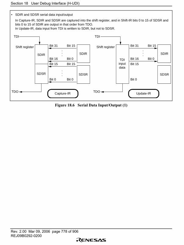
Section 18 User Debug Interface (H-UDI)
Rev. 2.00 Mar 09, 2006 page 778 of 906REJ09B0292-0200
TDI
SDIR
SDSR
SDIR
SDSR
SDIR
SDSR
TDO
Shift register Bit 31 Bit 15
Bit 16 Bit 0
Bit 15 Bit 15
Bit 0 Bit 0
• SDIR and SDSR serial data input/output
In Capture-IR, SDIR and SDSR are captured into the shift register, and in Shift-IR bits 0 to 15 of SDSR and bits 0 to 15 of SDIR are output in that order from TDO.
In Update-IR, data input from TDI is written to SDIR, but not to SDSR.
.
.
.
.
.
.
Capture-IR
TDI
TDIinputdata
TDO
Shift register Bit 31 Bit 15
Bit 16 Bit 0
Bit 15
Bit 0
.
.
.
Update-IR
Figure 18.6 Serial Data Input/Output (1)
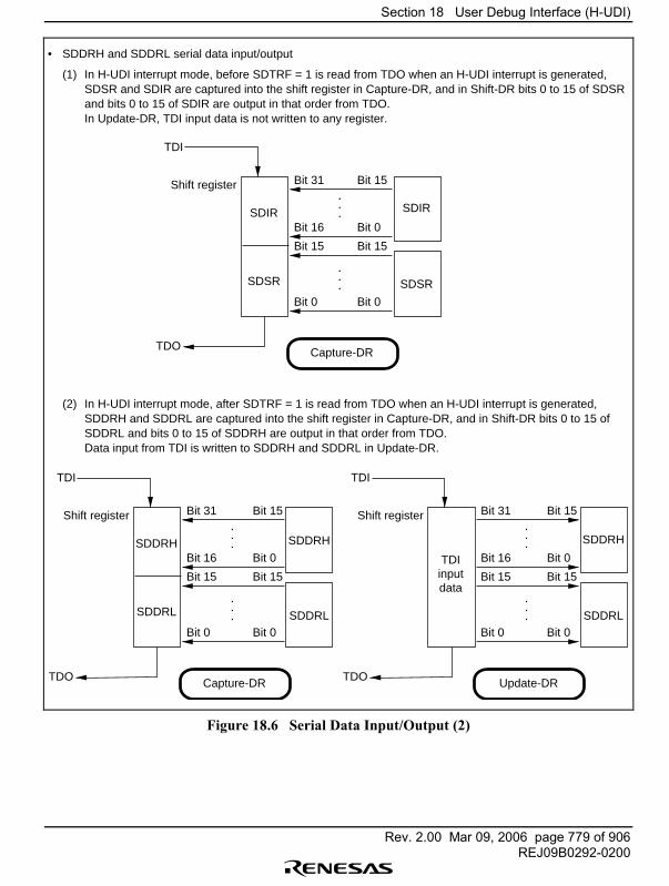
Section 18 User Debug Interface (H-UDI)
Rev. 2.00 Mar 09, 2006 page 779 of 906REJ09B0292-0200
TDI
SDDRH
SDDRL
SDDRH
SDDRL
TDO
Shift register Bit 31 Bit 15
Bit 16 Bit 0
Bit 15 Bit 15
Bit 0 Bit 0
Bit 15 Bit 15
Bit 0 Bit 0
.
.
.
.
.
....
Capture-DR
TDI
SDDRH
SDDRL
TDO
Shift register Bit 31 Bit 15
Bit 16 Bit 0
.
.
.
Update-DR
TDI
SDIR
SDSR
SDIR
SDSR
TDO
Shift register Bit 31 Bit 15
Bit 16 Bit 0
Bit 15 Bit 15
Bit 0 Bit 0
• SDDRH and SDDRL serial data input/output
(1) In H-UDI interrupt mode, before SDTRF = 1 is read from TDO when an H-UDI interrupt is generated, SDSR and SDIR are captured into the shift register in Capture-DR, and in Shift-DR bits 0 to 15 of SDSR and bits 0 to 15 of SDIR are output in that order from TDO.
In Update-DR, TDI input data is not written to any register.
(2) In H-UDI interrupt mode, after SDTRF = 1 is read from TDO when an H-UDI interrupt is generated, SDDRH and SDDRL are captured into the shift register in Capture-DR, and in Shift-DR bits 0 to 15 of SDDRL and bits 0 to 15 of SDDRH are output in that order from TDO.
Data input from TDI is written to SDDRH and SDDRL in Update-DR.
.
.
.
.
.
.
Capture-DR
TDIinputdata
Figure 18.6 Serial Data Input/Output (2)

Section 18 User Debug Interface (H-UDI)
Rev. 2.00 Mar 09, 2006 page 780 of 906REJ09B0292-0200
• SDIDR serial data input/output
In IDCODE mode, SDIDR is captured into the shift register in Capture-DR, and in Shift-DR bits 0 to 31 of SDIDR are output in that order from TDO.
In Update-DR, data input from TDI is not written to any register.
TDI
SDIDR SDIDR
TDO
Shift register Bit 31 Bit 15
Bit 0 Bit 0
.
.
.
.
Capture-DR
Figure 18.6 Serial Data Input/Output (3)
Section 19 Pin Function Controller (PFC)
Rev. 2.00 Mar 09, 2006 page 781 of 906REJ09B0292-0200
Section 19 Pin Function Controller (PFC)
19.1 Overview
The pin function controller (PFC) consists of registers to select multiplexed pin functions andinput/output direction. The pin function and input/output direction can be selected for individualpins regardless of the operating mode of the chip. Table 19.1 shows the chip�s multiplex pins.
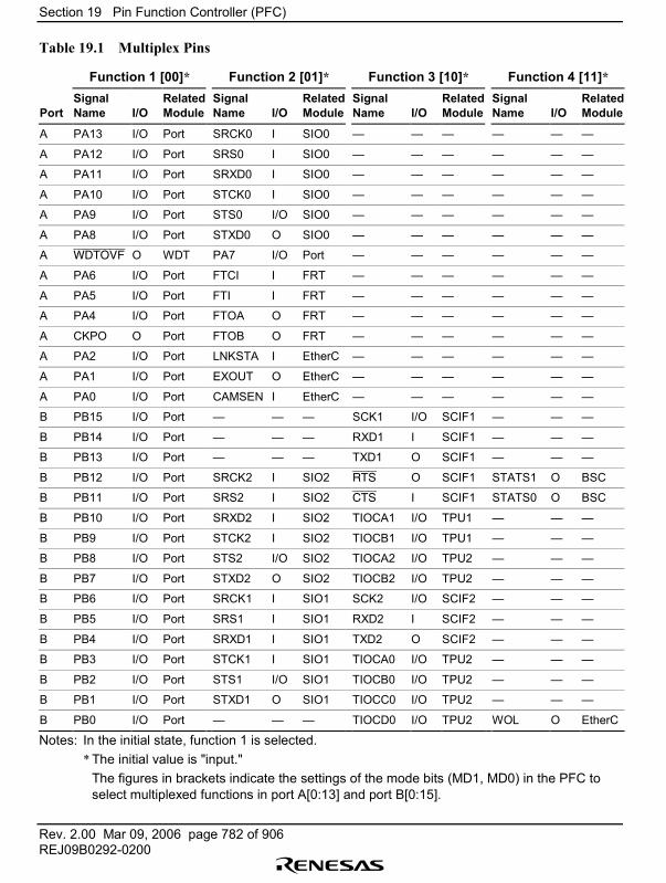
Section 19 Pin Function Controller (PFC)
Rev. 2.00 Mar 09, 2006 page 782 of 906REJ09B0292-0200
Table 19.1 Multiplex Pins
Function 1 [00]* Function 2 [01]* Function 3 [10]* Function 4 [11]*
PortSignalName I/O
RelatedModule
SignalName I/O
RelatedModule
SignalName I/O
RelatedModule
SignalName I/O
RelatedModule
A PA13 I/O Port SRCK0 I SIO0 � � � � � �
A PA12 I/O Port SRS0 I SIO0 � � � � � �
A PA11 I/O Port SRXD0 I SIO0 � � � � � �
A PA10 I/O Port STCK0 I SIO0 � � � � � �
A PA9 I/O Port STS0 I/O SIO0 � � � � � �
A PA8 I/O Port STXD0 O SIO0 � � � � � �
A WDTOVF O WDT PA7 I/O Port � � � � � �
A PA6 I/O Port FTCI I FRT � � � � � �
A PA5 I/O Port FTI I FRT � � � � � �
A PA4 I/O Port FTOA O FRT � � � � � �
A CKPO O Port FTOB O FRT � � � � � �
A PA2 I/O Port LNKSTA I EtherC � � � � � �
A PA1 I/O Port EXOUT O EtherC � � � � � �
A PA0 I/O Port CAMSEN I EtherC � � � � � �
B PB15 I/O Port � � � SCK1 I/O SCIF1 � � �
B PB14 I/O Port � � � RXD1 I SCIF1 � � �
B PB13 I/O Port � � � TXD1 O SCIF1 � � �
B PB12 I/O Port SRCK2 I SIO2 RTS O SCIF1 STATS1 O BSC
B PB11 I/O Port SRS2 I SIO2 CTS I SCIF1 STATS0 O BSC
B PB10 I/O Port SRXD2 I SIO2 TIOCA1 I/O TPU1 � � �
B PB9 I/O Port STCK2 I SIO2 TIOCB1 I/O TPU1 � � �
B PB8 I/O Port STS2 I/O SIO2 TIOCA2 I/O TPU2 � � �
B PB7 I/O Port STXD2 O SIO2 TIOCB2 I/O TPU2 � � �
B PB6 I/O Port SRCK1 I SIO1 SCK2 I/O SCIF2 � � �
B PB5 I/O Port SRS1 I SIO1 RXD2 I SCIF2 � � �
B PB4 I/O Port SRXD1 I SIO1 TXD2 O SCIF2 � � �
B PB3 I/O Port STCK1 I SIO1 TIOCA0 I/O TPU2 � � �
B PB2 I/O Port STS1 I/O SIO1 TIOCB0 I/O TPU2 � � �
B PB1 I/O Port STXD1 O SIO1 TIOCC0 I/O TPU2 � � �
B PB0 I/O Port � � � TIOCD0 I/O TPU2 WOL O EtherC
Notes: In the initial state, function 1 is selected.* The initial value is "input."
The figures in brackets indicate the settings of the mode bits (MD1, MD0) in the PFC to select multiplexed functions in port A[0:13] and port B[0:15].
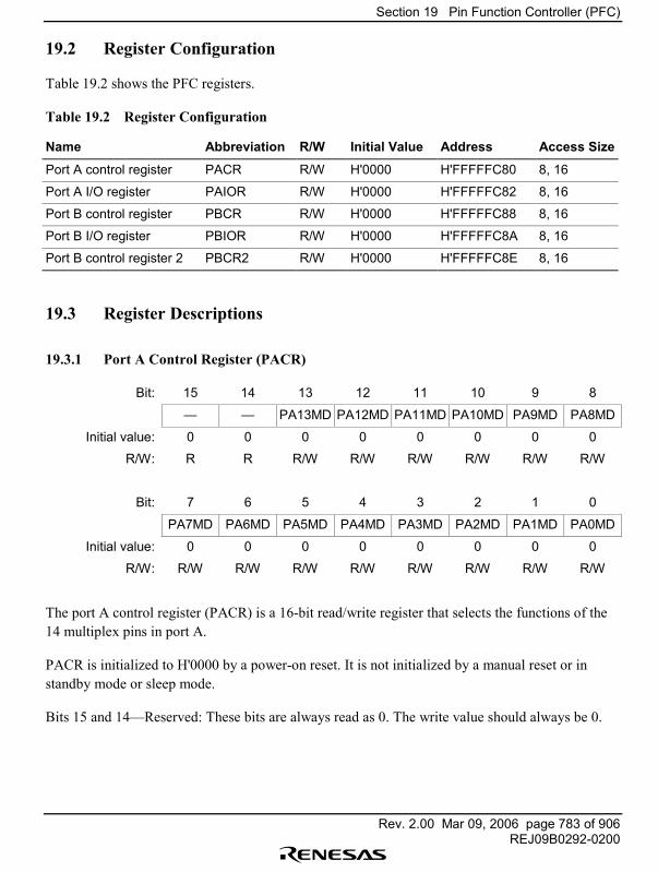
Section 19 Pin Function Controller (PFC)
Rev. 2.00 Mar 09, 2006 page 783 of 906REJ09B0292-0200
19.2 Register Configuration
Table 19.2 shows the PFC registers.
Table 19.2 Register Configuration
Name Abbreviation R/W Initial Value Address Access Size
Port A control register PACR R/W H'0000 H'FFFFFC80 8, 16
Port A I/O register PAIOR R/W H'0000 H'FFFFFC82 8, 16
Port B control register PBCR R/W H'0000 H'FFFFFC88 8, 16
Port B I/O register PBIOR R/W H'0000 H'FFFFFC8A 8, 16
Port B control register 2 PBCR2 R/W H'0000 H'FFFFFC8E 8, 16
19.3 Register Descriptions
19.3.1 Port A Control Register (PACR)
Bit: 15 14 13 12 11 10 9 8
� � PA13MD PA12MD PA11MD PA10MD PA9MD PA8MD
Initial value: 0 0 0 0 0 0 0 0
R/W: R R R/W R/W R/W R/W R/W R/W
Bit: 7 6 5 4 3 2 1 0
PA7MD PA6MD PA5MD PA4MD PA3MD PA2MD PA1MD PA0MD
Initial value: 0 0 0 0 0 0 0 0
R/W: R/W R/W R/W R/W R/W R/W R/W R/W
The port A control register (PACR) is a 16-bit read/write register that selects the functions of the14 multiplex pins in port A.
PACR is initialized to H'0000 by a power-on reset. It is not initialized by a manual reset or instandby mode or sleep mode.
Bits 15 and 14�Reserved: These bits are always read as 0. The write value should always be 0.
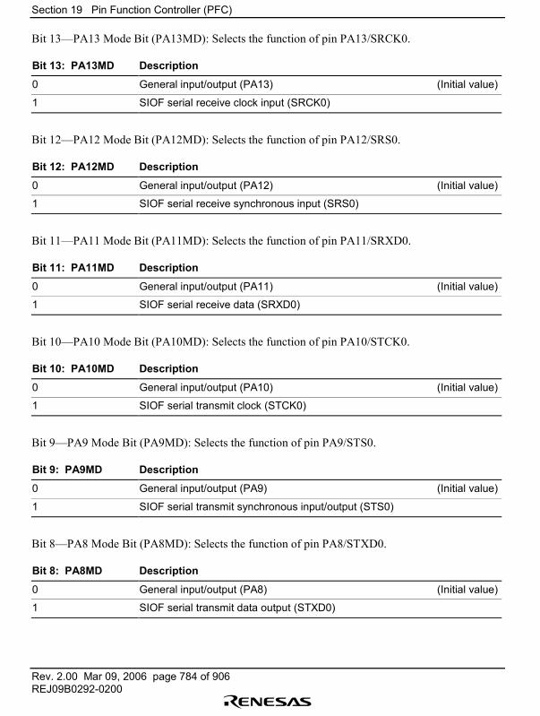
Section 19 Pin Function Controller (PFC)
Rev. 2.00 Mar 09, 2006 page 784 of 906REJ09B0292-0200
Bit 13�PA13 Mode Bit (PA13MD): Selects the function of pin PA13/SRCK0.
Bit 13: PA13MD Description
0 General input/output (PA13) (Initial value)
1 SIOF serial receive clock input (SRCK0)
Bit 12�PA12 Mode Bit (PA12MD): Selects the function of pin PA12/SRS0.
Bit 12: PA12MD Description
0 General input/output (PA12) (Initial value)
1 SIOF serial receive synchronous input (SRS0)
Bit 11�PA11 Mode Bit (PA11MD): Selects the function of pin PA11/SRXD0.
Bit 11: PA11MD Description
0 General input/output (PA11) (Initial value)
1 SIOF serial receive data (SRXD0)
Bit 10�PA10 Mode Bit (PA10MD): Selects the function of pin PA10/STCK0.
Bit 10: PA10MD Description
0 General input/output (PA10) (Initial value)
1 SIOF serial transmit clock (STCK0)
Bit 9�PA9 Mode Bit (PA9MD): Selects the function of pin PA9/STS0.
Bit 9: PA9MD Description
0 General input/output (PA9) (Initial value)
1 SIOF serial transmit synchronous input/output (STS0)
Bit 8�PA8 Mode Bit (PA8MD): Selects the function of pin PA8/STXD0.
Bit 8: PA8MD Description
0 General input/output (PA8) (Initial value)
1 SIOF serial transmit data output (STXD0)
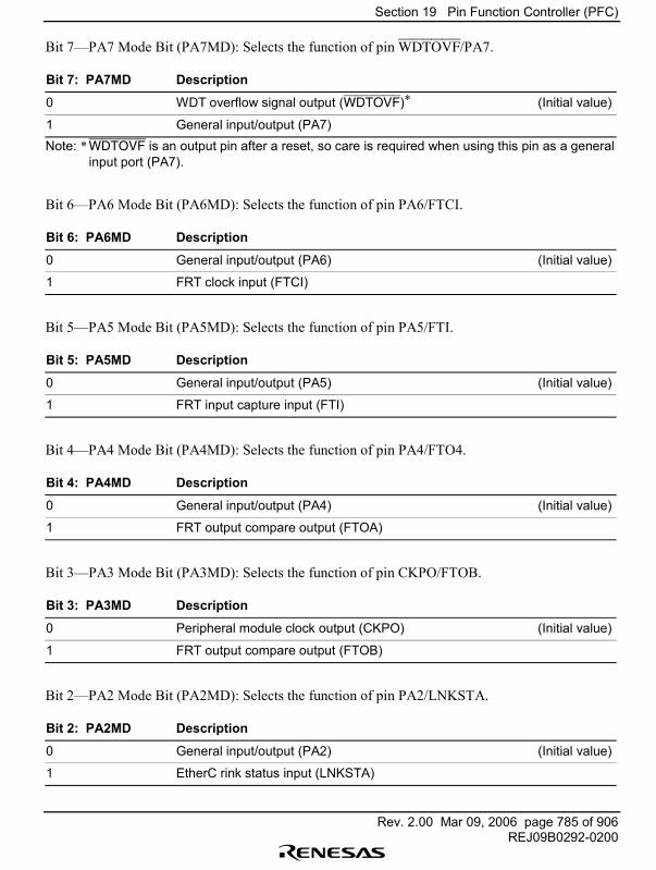
Section 19 Pin Function Controller (PFC)
Rev. 2.00 Mar 09, 2006 page 785 of 906REJ09B0292-0200
Bit 7�PA7 Mode Bit (PA7MD): Selects the function of pin WDTOVF/PA7.
Bit 7: PA7MD Description
0 WDT overflow signal output (WDTOVF)* (Initial value)
1 General input/output (PA7)Note: *WDTOVF is an output pin after a reset, so care is required when using this pin as a general
input port (PA7).
Bit 6�PA6 Mode Bit (PA6MD): Selects the function of pin PA6/FTCI.
Bit 6: PA6MD Description
0 General input/output (PA6) (Initial value)
1 FRT clock input (FTCI)
Bit 5�PA5 Mode Bit (PA5MD): Selects the function of pin PA5/FTI.
Bit 5: PA5MD Description
0 General input/output (PA5) (Initial value)
1 FRT input capture input (FTI)
Bit 4�PA4 Mode Bit (PA4MD): Selects the function of pin PA4/FTO4.
Bit 4: PA4MD Description
0 General input/output (PA4) (Initial value)
1 FRT output compare output (FTOA)
Bit 3�PA3 Mode Bit (PA3MD): Selects the function of pin CKPO/FTOB.
Bit 3: PA3MD Description
0 Peripheral module clock output (CKPO) (Initial value)
1 FRT output compare output (FTOB)
Bit 2�PA2 Mode Bit (PA2MD): Selects the function of pin PA2/LNKSTA.
Bit 2: PA2MD Description
0 General input/output (PA2) (Initial value)
1 EtherC rink status input (LNKSTA)
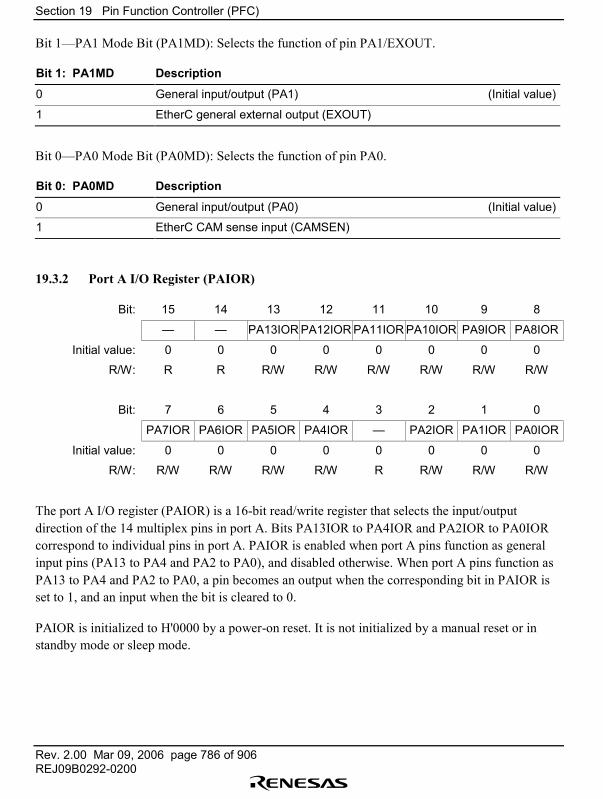
Section 19 Pin Function Controller (PFC)
Rev. 2.00 Mar 09, 2006 page 786 of 906REJ09B0292-0200
Bit 1�PA1 Mode Bit (PA1MD): Selects the function of pin PA1/EXOUT.
Bit 1: PA1MD Description
0 General input/output (PA1) (Initial value)
1 EtherC general external output (EXOUT)
Bit 0�PA0 Mode Bit (PA0MD): Selects the function of pin PA0.
Bit 0: PA0MD Description
0 General input/output (PA0) (Initial value)
1 EtherC CAM sense input (CAMSEN)
19.3.2 Port A I/O Register (PAIOR)
Bit: 15 14 13 12 11 10 9 8
� � PA13IOR PA12IOR PA11IOR PA10IOR PA9IOR PA8IOR
Initial value: 0 0 0 0 0 0 0 0
R/W: R R R/W R/W R/W R/W R/W R/W
Bit: 7 6 5 4 3 2 1 0
PA7IOR PA6IOR PA5IOR PA4IOR � PA2IOR PA1IOR PA0IOR
Initial value: 0 0 0 0 0 0 0 0
R/W: R/W R/W R/W R/W R R/W R/W R/W
The port A I/O register (PAIOR) is a 16-bit read/write register that selects the input/outputdirection of the 14 multiplex pins in port A. Bits PA13IOR to PA4IOR and PA2IOR to PA0IORcorrespond to individual pins in port A. PAIOR is enabled when port A pins function as generalinput pins (PA13 to PA4 and PA2 to PA0), and disabled otherwise. When port A pins function asPA13 to PA4 and PA2 to PA0, a pin becomes an output when the corresponding bit in PAIOR isset to 1, and an input when the bit is cleared to 0.
PAIOR is initialized to H'0000 by a power-on reset. It is not initialized by a manual reset or instandby mode or sleep mode.
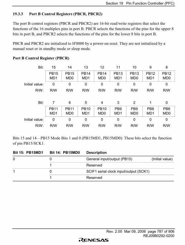
Section 19 Pin Function Controller (PFC)
Rev. 2.00 Mar 09, 2006 page 787 of 906REJ09B0292-0200
19.3.3 Port B Control Registers (PBCR, PBCR2)
The port B control registers (PBCR and PBCR2) are 16-bit read/write registers that select thefunctions of the 16 multiplex pins in port B. PBCR selects the functions of the pins for the upper 8bits in port B, and PBCR2 selects the functions of the pins for the lower 8 bits in port B.
PBCR and PBCR2 are initialized to H'0000 by a power-on reset. They are not initialized by amanual reset or in standby mode or sleep mode.
Port B Control Register (PBCR)
Bit: 15 14 13 12 11 10 9 8
PB15MD1
PB15MD0
PB14MD1
PB14MD0
PB13MD1
PB13MD0
PB12MD1
PB12MD0
Initial value: 0 0 0 0 0 0 0 0
R/W: R/W R/W R/W R/W R/W R/W R/W R/W
Bit: 7 6 5 4 3 2 1 0
PB11MD1
PB11MD0
PB10MD1
PB10MD0
PB9MD1
PB9MD0
PB8MD1
PB8MD0
Initial value: 0 0 0 0 0 0 0 0
R/W: R/W R/W R/W R/W R/W R/W R/W R/W
Bits 15 and 14�PB15 Mode Bits 1 and 0 (PB15MD1, PB15MD0): These bits select the functionof pin PB15/SCK1.
Bit 15: PB15MD1 Bit 14: PB15MD0 Description
0 0 General input/output (PB15) (Initial value)
1 Reserved
1 0 SCIF1 serial clock input/output (SCK1)
1 Reserved
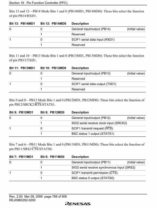
Section 19 Pin Function Controller (PFC)
Rev. 2.00 Mar 09, 2006 page 788 of 906REJ09B0292-0200
Bits 13 and 12�PB14 Mode Bits 1 and 0 (PB14MD1, PB14MD0): These bits select the functionof pin PB14/RXD1.
Bit 13: PB14MD1 Bit 12: PB14MD0 Description
0 0 General input/output (PB14) (Initial value)
1 Reserved
1 0 SCIF1 serial data input (RXD1)
1 Reserved
Bits 11 and 10�PB13 Mode Bits 1 and 0 (PB13MD1, PB13MD0): These bits select the functionof pin PB13/TXD1.
Bit 11: PB13MD1 Bit 10: PB13MD0 Description
0 0 General input/output (PB13) (Initial value)
1 Reserved
1 0 SCIF1 serial data output (TXD1)
1 Reserved
Bits 9 and 8�PB12 Mode Bits 1 and 0 (PB12MD1, PB12MD0): These bits select the function ofpin PB12/SRCK2/RTS/STATS1.
Bit 9: PB12MD1 Bit 8: PB12MD0 Description
0 0 General input/output (PB12) (Initial value)
1 SIO2 serial receive clock input (SRCK2)
1 0 SCIF1 transmit request (RTS)
1 BSC status 1 output (STATS1)
Bits 7 and 6�PB11 Mode Bits 1 and 0 (PB11MD1, PB11MD0): These bits select the function ofpin PB11/SRS2/CTS/STATS0.
Bit 7: PB11MD1 Bit 6: PB11MD0 Description
0 0 General input/output (PB11) (Initial value)
1 SIO2 serial receive synchronous input (SRS2)
1 0 SCIF1 transmit permission (CTS)
1 BSC status 0 output (STATS0)
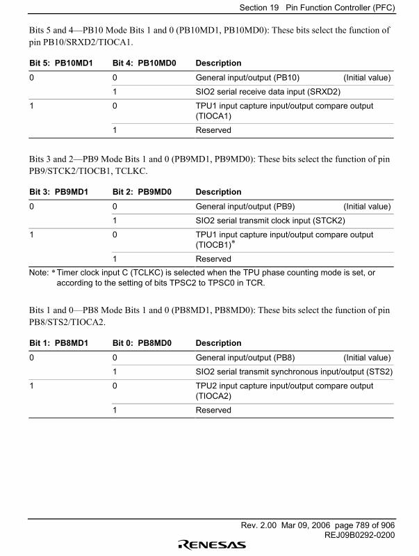
Section 19 Pin Function Controller (PFC)
Rev. 2.00 Mar 09, 2006 page 789 of 906REJ09B0292-0200
Bits 5 and 4�PB10 Mode Bits 1 and 0 (PB10MD1, PB10MD0): These bits select the function ofpin PB10/SRXD2/TIOCA1.
Bit 5: PB10MD1 Bit 4: PB10MD0 Description
0 0 General input/output (PB10) (Initial value)
1 SIO2 serial receive data input (SRXD2)
1 0 TPU1 input capture input/output compare output(TIOCA1)
1 Reserved
Bits 3 and 2�PB9 Mode Bits 1 and 0 (PB9MD1, PB9MD0): These bits select the function of pinPB9/STCK2/TIOCB1, TCLKC.
Bit 3: PB9MD1 Bit 2: PB9MD0 Description
0 0 General input/output (PB9) (Initial value)
1 SIO2 serial transmit clock input (STCK2)
1 0 TPU1 input capture input/output compare output(TIOCB1)*
1 ReservedNote: * Timer clock input C (TCLKC) is selected when the TPU phase counting mode is set, or
according to the setting of bits TPSC2 to TPSC0 in TCR.
Bits 1 and 0�PB8 Mode Bits 1 and 0 (PB8MD1, PB8MD0): These bits select the function of pinPB8/STS2/TIOCA2.
Bit 1: PB8MD1 Bit 0: PB8MD0 Description
0 0 General input/output (PB8) (Initial value)
1 SIO2 serial transmit synchronous input/output (STS2)
1 0 TPU2 input capture input/output compare output(TIOCA2)
1 Reserved
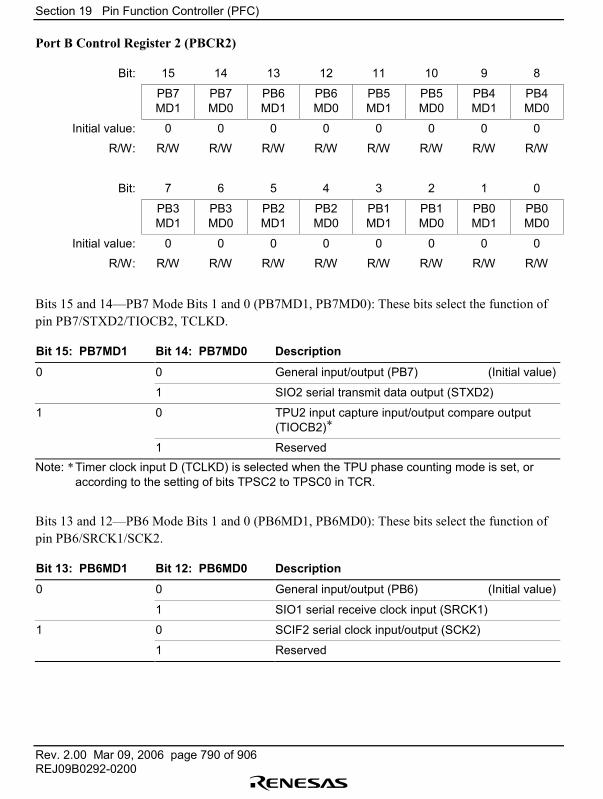
Section 19 Pin Function Controller (PFC)
Rev. 2.00 Mar 09, 2006 page 790 of 906REJ09B0292-0200
Port B Control Register 2 (PBCR2)
Bit: 15 14 13 12 11 10 9 8
PB7MD1
PB7MD0
PB6MD1
PB6MD0
PB5MD1
PB5MD0
PB4MD1
PB4MD0
Initial value: 0 0 0 0 0 0 0 0
R/W: R/W R/W R/W R/W R/W R/W R/W R/W
Bit: 7 6 5 4 3 2 1 0
PB3MD1
PB3MD0
PB2MD1
PB2MD0
PB1MD1
PB1MD0
PB0MD1
PB0MD0
Initial value: 0 0 0 0 0 0 0 0
R/W: R/W R/W R/W R/W R/W R/W R/W R/W
Bits 15 and 14�PB7 Mode Bits 1 and 0 (PB7MD1, PB7MD0): These bits select the function ofpin PB7/STXD2/TIOCB2, TCLKD.
Bit 15: PB7MD1 Bit 14: PB7MD0 Description
0 0 General input/output (PB7) (Initial value)
1 SIO2 serial transmit data output (STXD2)
1 0 TPU2 input capture input/output compare output(TIOCB2)*
1 ReservedNote: * Timer clock input D (TCLKD) is selected when the TPU phase counting mode is set, or
according to the setting of bits TPSC2 to TPSC0 in TCR.
Bits 13 and 12�PB6 Mode Bits 1 and 0 (PB6MD1, PB6MD0): These bits select the function ofpin PB6/SRCK1/SCK2.
Bit 13: PB6MD1 Bit 12: PB6MD0 Description
0 0 General input/output (PB6) (Initial value)
1 SIO1 serial receive clock input (SRCK1)
1 0 SCIF2 serial clock input/output (SCK2)
1 Reserved
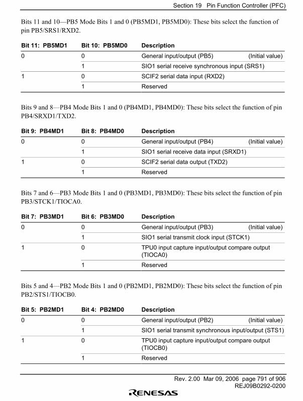
Section 19 Pin Function Controller (PFC)
Rev. 2.00 Mar 09, 2006 page 791 of 906REJ09B0292-0200
Bits 11 and 10�PB5 Mode Bits 1 and 0 (PB5MD1, PB5MD0): These bits select the function ofpin PB5/SRS1/RXD2.
Bit 11: PB5MD1 Bit 10: PB5MD0 Description
0 0 General input/output (PB5) (Initial value)
1 SIO1 serial receive synchronous input (SRS1)
1 0 SCIF2 serial data input (RXD2)
1 Reserved
Bits 9 and 8�PB4 Mode Bits 1 and 0 (PB4MD1, PB4MD0): These bits select the function of pinPB4/SRXD1/TXD2.
Bit 9: PB4MD1 Bit 8: PB4MD0 Description
0 0 General input/output (PB4) (Initial value)
1 SIO1 serial receive data input (SRXD1)
1 0 SCIF2 serial data output (TXD2)
1 Reserved
Bits 7 and 6�PB3 Mode Bits 1 and 0 (PB3MD1, PB3MD0): These bits select the function of pinPB3/STCK1/TIOCA0.
Bit 7: PB3MD1 Bit 6: PB3MD0 Description
0 0 General input/output (PB3) (Initial value)
1 SIO1 serial transmit clock input (STCK1)
1 0 TPU0 input capture input/output compare output(TIOCA0)
1 Reserved
Bits 5 and 4�PB2 Mode Bits 1 and 0 (PB2MD1, PB2MD0): These bits select the function of pinPB2/STS1/TIOCB0.
Bit 5: PB2MD1 Bit 4: PB2MD0 Description
0 0 General input/output (PB2) (Initial value)
1 SIO1 serial transmit synchronous input/output (STS1)
1 0 TPU0 input capture input/output compare output(TIOCB0)
1 Reserved
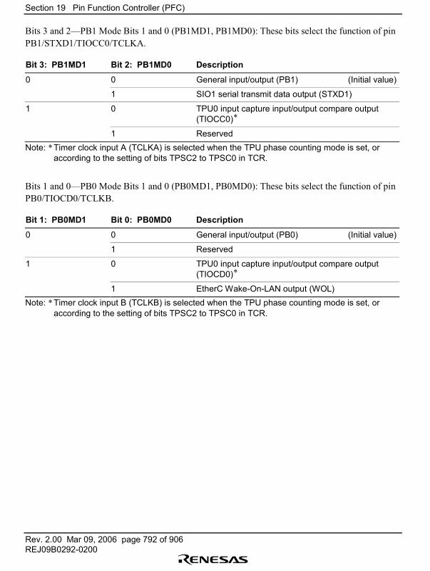
Section 19 Pin Function Controller (PFC)
Rev. 2.00 Mar 09, 2006 page 792 of 906REJ09B0292-0200
Bits 3 and 2�PB1 Mode Bits 1 and 0 (PB1MD1, PB1MD0): These bits select the function of pinPB1/STXD1/TIOCC0/TCLKA.
Bit 3: PB1MD1 Bit 2: PB1MD0 Description
0 0 General input/output (PB1) (Initial value)
1 SIO1 serial transmit data output (STXD1)
1 0 TPU0 input capture input/output compare output(TIOCC0)*
1 ReservedNote: * Timer clock input A (TCLKA) is selected when the TPU phase counting mode is set, or
according to the setting of bits TPSC2 to TPSC0 in TCR.
Bits 1 and 0�PB0 Mode Bits 1 and 0 (PB0MD1, PB0MD0): These bits select the function of pinPB0/TIOCD0/TCLKB.
Bit 1: PB0MD1 Bit 0: PB0MD0 Description
0 0 General input/output (PB0) (Initial value)
1 Reserved
1 0 TPU0 input capture input/output compare output(TIOCD0)*
1 EtherC Wake-On-LAN output (WOL)Note: * Timer clock input B (TCLKB) is selected when the TPU phase counting mode is set, or
according to the setting of bits TPSC2 to TPSC0 in TCR.

Section 19 Pin Function Controller (PFC)
Rev. 2.00 Mar 09, 2006 page 793 of 906REJ09B0292-0200
19.3.4 Port B I/O Register (PBIOR)
Bit: 15 14 13 12 11 10 9 8
PB15IOR
PB14IOR
PB13IOR
PB12IOR
PB11IOR
PB10IOR
PB9IOR
PB8IOR
Initial value: 0 0 0 0 0 0 0 0
R/W: R/W R/W R/W R/W R/W R/W R/W R/W
Bit: 7 6 5 4 3 2 1 0
PB7IOR
PB6IOR
PB5IOR
PB4IOR
PB3IOR
PB2IOR
PB1IOR
PB0IOR
Initial value: 0 0 0 0 0 0 0 0
R/W: R/W R/W R/W R/W R/W R/W R/W R/W
The port B I/O register (PBIOR) is a 16-bit read/write register that selects the input/outputdirection of the 16 multiplex pins in port B. Bits PB15IOR to PB0IOR correspond to individualpins in port B. PBIOR is enabled when port B pins function as general input pins (PB15 to PB0),and disabled otherwise. When port B pins function as PB15 to PB0, a pin becomes an output whenthe corresponding bit in PBIOR is set to 1, and an input when the bit is cleared to 0.
PBIOR is initialized to H'0000 by a power-on reset. It is not initialized by a manual reset or instandby mode or sleep mode.
Section 19 Pin Function Controller (PFC)
Rev. 2.00 Mar 09, 2006 page 794 of 906REJ09B0292-0200
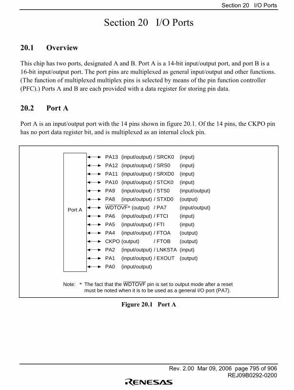
Section 20 I/O Ports
Rev. 2.00 Mar 09, 2006 page 795 of 906REJ09B0292-0200
Section 20 I/O Ports
20.1 Overview
This chip has two ports, designated A and B. Port A is a 14-bit input/output port, and port B is a16-bit input/output port. The port pins are multiplexed as general input/output and other functions.(The function of multiplexed multiplex pins is selected by means of the pin function controller(PFC).) Ports A and B are each provided with a data register for storing pin data.
20.2 Port A
Port A is an input/output port with the 14 pins shown in figure 20.1. Of the 14 pins, the CKPO pinhas no port data register bit, and is multiplexed as an internal clock pin.
PA13 (input/output) / SRCK0 (input)
PA12 (input/output) / SRS0 (input)
PA11 (input/output) / SRXD0 (input)
PA10 (input/output) / STCK0 (input)
PA9 (input/output) / STS0 (input/output)
PA8 (input/output) / STXD0 (output)
WDTOVF* (output) / PA7 (input/output)
PA6 (input/output) / FTCI (input)
PA5 (input/output) / FTI (input)
PA4 (input/output) / FTOA (output)
CKPO (output) / FTOB (output)
PA2 (input/output) / LNKSTA (input)
PA1 (input/output) / EXOUT (output)
PA0 (input/output)
Port A
Note: * The fact that the WDTOVF pin is set to output mode after a reset must be noted when it is to be used as a general I/O port (PA7).
Figure 20.1 Port A
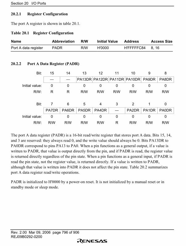
Section 20 I/O Ports
Rev. 2.00 Mar 09, 2006 page 796 of 906REJ09B0292-0200
20.2.1 Register Configuration
The port A register is shown in table 20.1.
Table 20.1 Register Configuration
Name Abbreviation R/W Initial Value Address Access Size
Port A data register PADR R/W H'0000 H'FFFFFC84 8, 16
20.2.2 Port A Data Register (PADR)
Bit: 15 14 13 12 11 10 9 8
� � PA13DR PA12DR PA11DR PA10DR PA9DR PA8DR
Initial value: 0 0 0 0 0 0 0 0
R/W: R R R/W R/W R/W R/W R/W R/W
Bit: 7 6 5 4 3 2 1 0
PA7DR PA6DR PA5DR PA4DR � PA2DR PA1DR PA0DR
Initial value: 0 0 0 0 0 0 0 0
R/W: R/W R/W R/W R/W R R/W R/W R/W
The port A data register (PADR) is a 16-bit read/write register that stores port A data. Bits 15, 14,and 3 are reserved: they always read 0, and the write value should always be 0. Bits PA13DR toPA0DR correspond to pins PA13 to PA0. When a pin functions as a general output, if a value iswritten to PADR, that value is output directly from the pin, and if PADR is read, the register valueis returned directly regardless of the pin state. When a pin functions as a general input, if PADR isread the pin state, not the register value, is returned directly. If a value is written to PADR,although that value is written into PADR it does not affect the pin state. Table 20.2 summarizesport A data register read/write operations.
PADR is initialized to H'0000 by a power-on reset. It is not initialized by a manual reset or instandby mode or sleep mode.
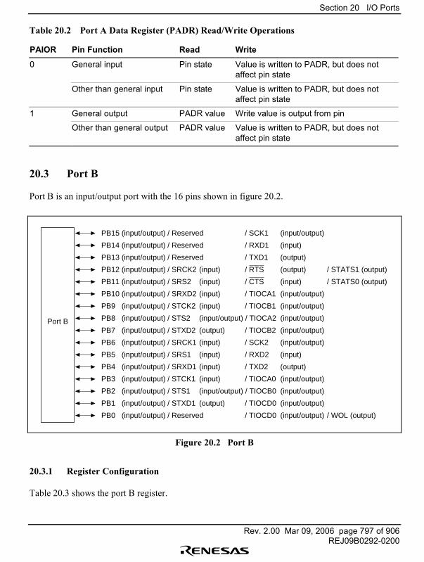
Section 20 I/O Ports
Rev. 2.00 Mar 09, 2006 page 797 of 906REJ09B0292-0200
Table 20.2 Port A Data Register (PADR) Read/Write Operations
PAIOR Pin Function Read Write
0 General input Pin state Value is written to PADR, but does notaffect pin state
Other than general input Pin state Value is written to PADR, but does notaffect pin state
1 General output PADR value Write value is output from pin
Other than general output PADR value Value is written to PADR, but does notaffect pin state
20.3 Port B
Port B is an input/output port with the 16 pins shown in figure 20.2.
PB15 (input/output)
PB14 (input/output)
PB13 (input/output)
PB12 (input/output)
PB11 (input/output)
PB10 (input/output)
PB9 (input/output)
PB8 (input/output)
PB7 (input/output)
PB6 (input/output)
PB5 (input/output)
PB4 (input/output)
PB3 (input/output)
PB2 (input/output)
PB1 (input/output)
PB0 (input/output)
/ Reserved / SCK1 (input/output)
/ Reserved / RXD1 (input)
/ Reserved / TXD1 (output)
/ SRCK2 (input) / RTS (output) / STATS1 (output)
/ SRS2 (input) / CTS (input) / STATS0 (output)
/ SRXD2 (input) / TIOCA1 (input/output)
/ STCK2 (input) / TIOCB1 (input/output)
/ STS2 (input/output) / TIOCA2 (input/output)
/ STXD2 (output) / TIOCB2 (input/output)
/ SRCK1 (input) / SCK2 (input/output)
/ SRS1 (input) / RXD2 (input)
/ SRXD1 (input) / TXD2 (output)
/ STCK1 (input) / TIOCA0 (input/output)
/ STS1 (input/output) / TIOCB0 (input/output)
/ STXD1 (output) / TIOCD0 (input/output)
/ Reserved / TIOCD0 (input/output) / WOL (output)
Port B
Figure 20.2 Port B
20.3.1 Register Configuration
Table 20.3 shows the port B register.
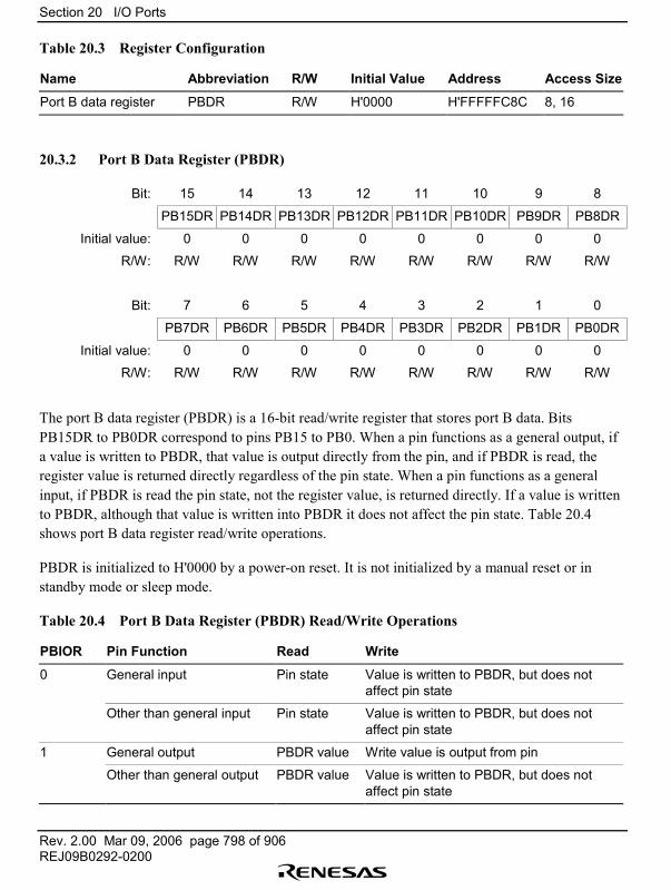
Section 20 I/O Ports
Rev. 2.00 Mar 09, 2006 page 798 of 906REJ09B0292-0200
Table 20.3 Register Configuration
Name Abbreviation R/W Initial Value Address Access Size
Port B data register PBDR R/W H'0000 H'FFFFFC8C 8, 16
20.3.2 Port B Data Register (PBDR)
Bit: 15 14 13 12 11 10 9 8
PB15DR PB14DR PB13DR PB12DR PB11DR PB10DR PB9DR PB8DR
Initial value: 0 0 0 0 0 0 0 0
R/W: R/W R/W R/W R/W R/W R/W R/W R/W
Bit: 7 6 5 4 3 2 1 0
PB7DR PB6DR PB5DR PB4DR PB3DR PB2DR PB1DR PB0DR
Initial value: 0 0 0 0 0 0 0 0
R/W: R/W R/W R/W R/W R/W R/W R/W R/W
The port B data register (PBDR) is a 16-bit read/write register that stores port B data. BitsPB15DR to PB0DR correspond to pins PB15 to PB0. When a pin functions as a general output, ifa value is written to PBDR, that value is output directly from the pin, and if PBDR is read, theregister value is returned directly regardless of the pin state. When a pin functions as a generalinput, if PBDR is read the pin state, not the register value, is returned directly. If a value is writtento PBDR, although that value is written into PBDR it does not affect the pin state. Table 20.4shows port B data register read/write operations.
PBDR is initialized to H'0000 by a power-on reset. It is not initialized by a manual reset or instandby mode or sleep mode.
Table 20.4 Port B Data Register (PBDR) Read/Write Operations
PBIOR Pin Function Read Write
0 General input Pin state Value is written to PBDR, but does notaffect pin state
Other than general input Pin state Value is written to PBDR, but does notaffect pin state
1 General output PBDR value Write value is output from pin
Other than general output PBDR value Value is written to PBDR, but does notaffect pin state
Section 21 Power-Down Modes
Rev. 2.00 Mar 09, 2006 page 799 of 906REJ09B0292-0200
Section 21 Power-Down Modes
21.1 Overview
This chip has a module standby function (which reduces power consumption by selectively haltingoperation of unnecessary modules among the on-chip peripheral modules and the DSP unit), asleep mode (which halts CPU functions), and a standby mode (which halts all functions).
21.1.1 Power-Down Modes
The following modes and function are provided as power-down modes:
1. Sleep mode2. Standby mode3. Module standby function
(UBC, DMAC, DSP, FRT, SCIF1�2, TPU, SIOF, SIO1�2)
Table 21.1 shows the transition conditions for entering the modes from the program executionstate, as well as the CPU and peripheral module states in each mode and the procedures forcanceling each mode.
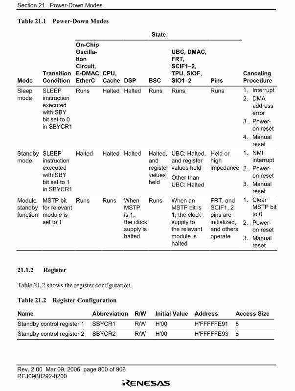
Section 21 Power-Down Modes
Rev. 2.00 Mar 09, 2006 page 800 of 906REJ09B0292-0200
Table 21.1 Power-Down Modes
State
ModeTransitionCondition
On-ChipOscilla-tionCircuit,E-DMAC,EtherC
CPU,Cache DSP BSC
UBC, DMAC,FRT,SCIF1�2,TPU, SIOF,SIO1�2 Pins
CancelingProcedure
Sleepmode
SLEEPinstructionexecutedwith SBYbit set to 0in SBYCR1
Runs Halted Halted Runs Runs Runs 1. Interrupt2. DMA
addresserror
3. Power-on reset
4. Manualreset
Standbymode
SLEEPinstructionexecutedwith SBYbit set to 1in SBYCR1
Halted Halted Halted Halted,andregistervaluesheld
UBC: Halted,and registervalues held
Other thanUBC: Halted
Held orhighimpedance
1. NMIinterrupt
2. Power-on reset
3. Manualreset
Modulestandbyfunction
MSTP bitfor relevantmodule isset to 1
Runs Runs WhenMSTPis 1,the clocksupply ishalted
Runs When anMSTP bit is1, the clocksupply tothe relevantmodule ishalted
FRT, andSCIF1, 2pins areinitialized,and othersoperate
1. ClearMSTP bitto 0
2. Power-on reset
3. Manualreset
21.1.2 Register
Table 21.2 shows the register configuration.
Table 21.2 Register Configuration
Name Abbreviation R/W Initial Value Address Access Size
Standby control register 1 SBYCR1 R/W H'00 H'FFFFFE91 8
Standby control register 2 SBYCR2 R/W H'00 H'FFFFFE93 8
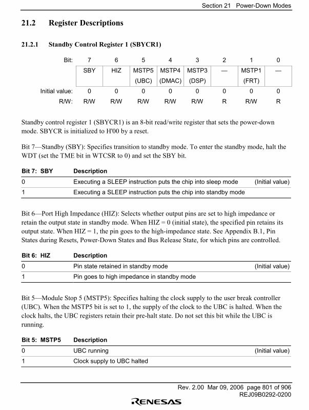
Section 21 Power-Down Modes
Rev. 2.00 Mar 09, 2006 page 801 of 906REJ09B0292-0200
21.2 Register Descriptions
21.2.1 Standby Control Register 1 (SBYCR1)
Bit: 7 6 5 4 3 2 1 0
SBY HIZ MSTP5 MSTP4 MSTP3 � MSTP1 �
(UBC) (DMAC) (DSP) (FRT)
Initial value: 0 0 0 0 0 0 0 0
R/W: R/W R/W R/W R/W R/W R R/W R
Standby control register 1 (SBYCR1) is an 8-bit read/write register that sets the power-downmode. SBYCR is initialized to H'00 by a reset.
Bit 7�Standby (SBY): Specifies transition to standby mode. To enter the standby mode, halt theWDT (set the TME bit in WTCSR to 0) and set the SBY bit.
Bit 7: SBY Description
0 Executing a SLEEP instruction puts the chip into sleep mode (Initial value)
1 Executing a SLEEP instruction puts the chip into standby mode
Bit 6�Port High Impedance (HIZ): Selects whether output pins are set to high impedance orretain the output state in standby mode. When HIZ = 0 (initial state), the specified pin retains itsoutput state. When HIZ = 1, the pin goes to the high-impedance state. See Appendix B.1, PinStates during Resets, Power-Down States and Bus Release State, for which pins are controlled.
Bit 6: HIZ Description
0 Pin state retained in standby mode (Initial value)
1 Pin goes to high impedance in standby mode
Bit 5�Module Stop 5 (MSTP5): Specifies halting the clock supply to the user break controller(UBC). When the MSTP5 bit is set to 1, the supply of the clock to the UBC is halted. When theclock halts, the UBC registers retain their pre-halt state. Do not set this bit while the UBC isrunning.
Bit 5: MSTP5 Description
0 UBC running (Initial value)
1 Clock supply to UBC halted
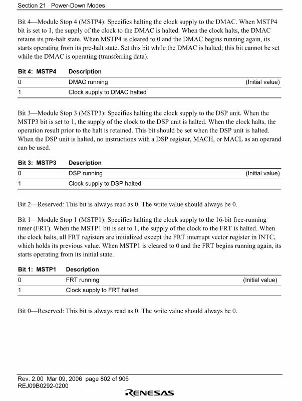
Section 21 Power-Down Modes
Rev. 2.00 Mar 09, 2006 page 802 of 906REJ09B0292-0200
Bit 4�Module Stop 4 (MSTP4): Specifies halting the clock supply to the DMAC. When MSTP4bit is set to 1, the supply of the clock to the DMAC is halted. When the clock halts, the DMACretains its pre-halt state. When MSTP4 is cleared to 0 and the DMAC begins running again, itsstarts operating from its pre-halt state. Set this bit while the DMAC is halted; this bit cannot be setwhile the DMAC is operating (transferring data).
Bit 4: MSTP4 Description
0 DMAC running (Initial value)
1 Clock supply to DMAC halted
Bit 3�Module Stop 3 (MSTP3): Specifies halting the clock supply to the DSP unit. When theMSTP3 bit is set to 1, the supply of the clock to the DSP unit is halted. When the clock halts, theoperation result prior to the halt is retained. This bit should be set when the DSP unit is halted.When the DSP unit is halted, no instructions with a DSP register, MACH, or MACL as an operandcan be used.
Bit 3: MSTP3 Description
0 DSP running (Initial value)
1 Clock supply to DSP halted
Bit 2�Reserved: This bit is always read as 0. The write value should always be 0.
Bit 1�Module Stop 1 (MSTP1): Specifies halting the clock supply to the 16-bit free-runningtimer (FRT). When the MSTP1 bit is set to 1, the supply of the clock to the FRT is halted. Whenthe clock halts, all FRT registers are initialized except the FRT interrupt vector register in INTC,which holds its previous value. When MSTP1 is cleared to 0 and the FRT begins running again, itsstarts operating from its initial state.
Bit 1: MSTP1 Description
0 FRT running (Initial value)
1 Clock supply to FRT halted
Bit 0�Reserved: This bit is always read as 0. The write value should always be 0.

Section 21 Power-Down Modes
Rev. 2.00 Mar 09, 2006 page 803 of 906REJ09B0292-0200
21.2.2 Standby Control Register 2 (SBYCR2)
Bit: 7 6 5 4 3 2 1 0
� � MSTP11(TPU)
MSTP10(SIO2)
MSTP9(SIO1)
MSTP8(SIOF)
MSTP7(SCIF2)
MSTP6(SCIF1)
Initial value: 0 0 0 0 0 0 0 0
R/W: R R R/W R/W R/W R/W R/W R/W
Standby control register 2 (SBYCR2) is an 8-bit read/write register that sets the power-down modestate. SBYCR2 is initialized to H'00 by a reset.
Bits 7 and 6�Reserved: These bits are always read as 0. The write value should always be 0.
Bit 5�Module Stop 11 (MSTP11): Specifies halting the clock supply to the 16-bit timer pulseunit (TPU). When the MSTP11 bit is set to 1, the supply of the clock to the TPU is halted. Whenthe clock halts, the TPU retains its pre-halt state, and the TPU interrupt vector register in the INTCretains its pre-halt value. Therefore, when MSTP11 is cleared to 0 and the clock supply to the TPUis resumed, the TPU starts operating again.
Bit 5: MSTP11 Description
0 TPU running (Initial value)
1 Clock supply to TPU halted
Bit 4�Module Stop 10 (MSTP10): Specifies halting the clock supply to SIO channel 2. When theMSTP10 bit is set to 1, the supply of the clock to SIO channel 2 is halted. When the clock halts,SIO channel 2 retains its pre-halt state, and the SIO channel 2 interrupt vector register in the INTCretains its pre-halt value. Therefore, when MSTP10 is cleared to 0 and the clock supply to SIOchannel 2 is restarted, operation starts again.
Bit 4: MSTP10 Description
0 SIO channel 2 running (Initial value)
1 Clock supply to SIO channel 2 halted
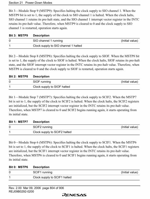
Section 21 Power-Down Modes
Rev. 2.00 Mar 09, 2006 page 804 of 906REJ09B0292-0200
Bit 3�Module Stop 9 (MSTP9): Specifies halting the clock supply to SIO channel 1. When theMSTP9 bit is set to 1, the supply of the clock to SIO channel 1 is halted. When the clock halts,SIO channel 1 retains its pre-halt state, and the SIO channel 1 interrupt vector register in the INTCretains its pre-halt value. Therefore, when MSTP9 is cleared to 0 and the clock supply to SIOchannel 1 is restarted, operation starts again.
Bit 3: MSTP9 Description
0 SIO channel 1 running (Initial value)
1 Clock supply to SIO channel 1 halted
Bit 2�Module Stop 8 (MSTP8): Specifies halting the clock supply to SIOF. When the MSTP8 bitis set to 1, the supply of the clock to SIOF is halted. When the clock halts, SIOF retains its pre-haltstate, and the SIOF interrupt vector register in the INTC retains its pre-halt value. Therefore, whenMSTP8 is cleared to 0 and the clock supply to SIOF is restarted, operation starts again.
Bit 2: MSTP8 Description
0 SIOF running (Initial value)
1 Clock supply to SIOF halted
Bit 1�Module Stop 7 (MSTP7): Specifies halting the clock supply to SCIF2. When the MSTP7bit is set to 1, the supply of the clock to SCIF2 is halted. When the clock halts, the SCIF2 registersare initialized, but the SCIF2 interrupt vector register in the INTC retains its pre-halt value.Therefore, when MSTP7 is cleared to 0 and SCIF2 begins running again, it starts operating fromits initial state.
Bit 1: MSTP7 Description
0 SCIF2 running (Initial value)
1 Clock supply to SCIF2 halted
Bit 0�Module Stop 6 (MSTP6): Specifies halting the clock supply to SCIF1. When the MSTP6bit is set to 1, the supply of the clock to SCIF1 is halted. When the clock halts, the SCIF1 registersare initialized, but the SCIF1 interrupt vector register in the INTC retains its pre-halt value.Therefore, when MSTP6 is cleared to 0 and SCIF1 begins running again, it starts operating fromits initial state.
Bit 0: MSTP6 Description
0 SCIF1 running (Initial value)
1 Clock supply to SCIF1 halted
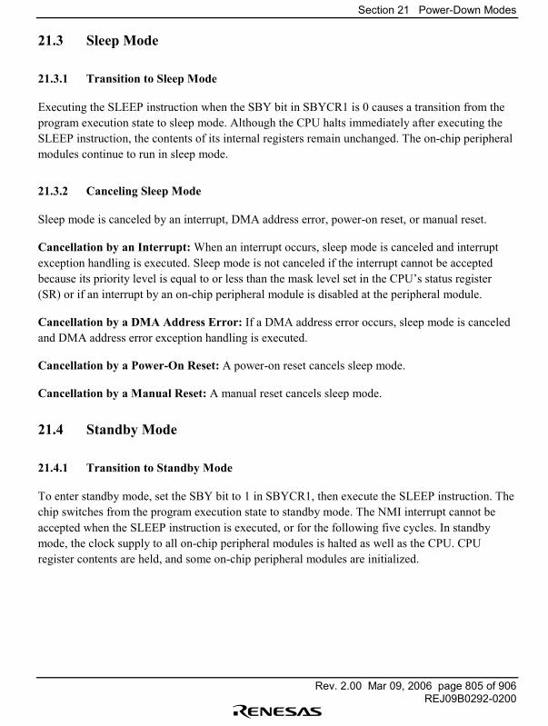
Section 21 Power-Down Modes
Rev. 2.00 Mar 09, 2006 page 805 of 906REJ09B0292-0200
21.3 Sleep Mode
21.3.1 Transition to Sleep Mode
Executing the SLEEP instruction when the SBY bit in SBYCR1 is 0 causes a transition from theprogram execution state to sleep mode. Although the CPU halts immediately after executing theSLEEP instruction, the contents of its internal registers remain unchanged. The on-chip peripheralmodules continue to run in sleep mode.
21.3.2 Canceling Sleep Mode
Sleep mode is canceled by an interrupt, DMA address error, power-on reset, or manual reset.
Cancellation by an Interrupt: When an interrupt occurs, sleep mode is canceled and interruptexception handling is executed. Sleep mode is not canceled if the interrupt cannot be acceptedbecause its priority level is equal to or less than the mask level set in the CPU�s status register(SR) or if an interrupt by an on-chip peripheral module is disabled at the peripheral module.
Cancellation by a DMA Address Error: If a DMA address error occurs, sleep mode is canceledand DMA address error exception handling is executed.
Cancellation by a Power-On Reset: A power-on reset cancels sleep mode.
Cancellation by a Manual Reset: A manual reset cancels sleep mode.
21.4 Standby Mode
21.4.1 Transition to Standby Mode
To enter standby mode, set the SBY bit to 1 in SBYCR1, then execute the SLEEP instruction. Thechip switches from the program execution state to standby mode. The NMI interrupt cannot beaccepted when the SLEEP instruction is executed, or for the following five cycles. In standbymode, the clock supply to all on-chip peripheral modules is halted as well as the CPU. CPUregister contents are held, and some on-chip peripheral modules are initialized.
Section 21 Power-Down Modes
Rev. 2.00 Mar 09, 2006 page 806 of 906REJ09B0292-0200
Table 21.3 Register States in Standby Mode
Module Registers InitializedRegisters that RetainData
Registerswith UndefinedContents
Interrupt controller (INTC) � All registers �User break controller (UBC) � All registers �Bus state controller (BSC) � All registers �Direct memory accesscontroller (DMAC)
DMA channel controlregister 0, 1DMA operation register
• DMA sourceaddress registers 0and 1
• DMA destinationaddress registers 0and 1
• DMA transfer countregisters 0 and 1
• DMA request/response selectioncontrol registers 0and 1
• Vector numbersetting registersDMA0 and DMA1
�
Watchdog timer (WDT) Bits 7�5 of the timercontrol/status register
Bits 2�0 of the timercontrol/status register
�
Reset control/statusregister
Timer counter
16-bit free-running timer (FRT) All registers � �Serial communication interfacewith FIFO (SCIF1�2)
All registers � �
Serial I/O with FIFO (SIOF) � All registers �Serial I/O (SIO1�2) � All registers �User debug interface(H-UDI)
� All registers �
16-bit timer pulse unit (TPU) � All registers �Pin function controller (PFC) � All registers �Ethernet controller directmemory access controller (E-DMAC)
All registers � �
Ethernet controller (EtherC) All registers � �Others � Standby control register
1, 2Frequency modificationregister
�
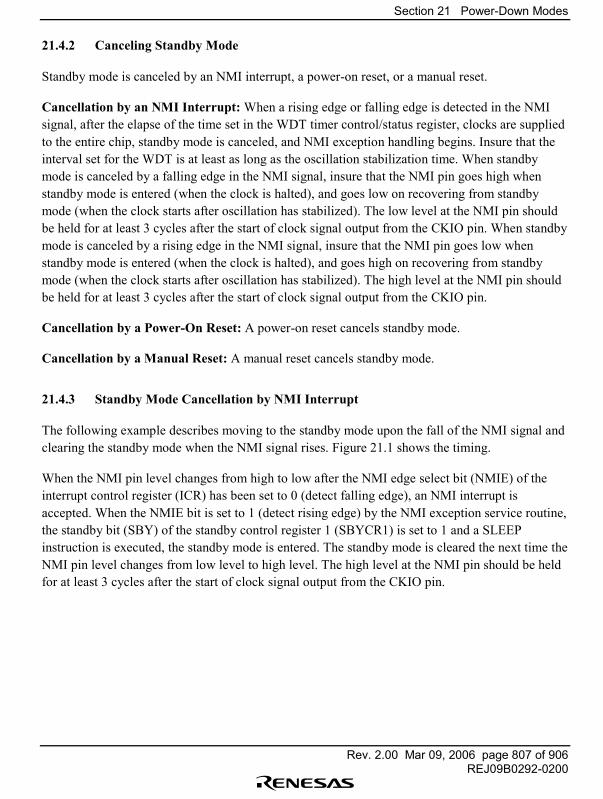
Section 21 Power-Down Modes
Rev. 2.00 Mar 09, 2006 page 807 of 906REJ09B0292-0200
21.4.2 Canceling Standby Mode
Standby mode is canceled by an NMI interrupt, a power-on reset, or a manual reset.
Cancellation by an NMI Interrupt: When a rising edge or falling edge is detected in the NMIsignal, after the elapse of the time set in the WDT timer control/status register, clocks are suppliedto the entire chip, standby mode is canceled, and NMI exception handling begins. Insure that theinterval set for the WDT is at least as long as the oscillation stabilization time. When standbymode is canceled by a falling edge in the NMI signal, insure that the NMI pin goes high whenstandby mode is entered (when the clock is halted), and goes low on recovering from standbymode (when the clock starts after oscillation has stabilized). The low level at the NMI pin shouldbe held for at least 3 cycles after the start of clock signal output from the CKIO pin. When standbymode is canceled by a rising edge in the NMI signal, insure that the NMI pin goes low whenstandby mode is entered (when the clock is halted), and goes high on recovering from standbymode (when the clock starts after oscillation has stabilized). The high level at the NMI pin shouldbe held for at least 3 cycles after the start of clock signal output from the CKIO pin.
Cancellation by a Power-On Reset: A power-on reset cancels standby mode.
Cancellation by a Manual Reset: A manual reset cancels standby mode.
21.4.3 Standby Mode Cancellation by NMI Interrupt
The following example describes moving to the standby mode upon the fall of the NMI signal andclearing the standby mode when the NMI signal rises. Figure 21.1 shows the timing.
When the NMI pin level changes from high to low after the NMI edge select bit (NMIE) of theinterrupt control register (ICR) has been set to 0 (detect falling edge), an NMI interrupt isaccepted. When the NMIE bit is set to 1 (detect rising edge) by the NMI exception service routine,the standby bit (SBY) of the standby control register 1 (SBYCR1) is set to 1 and a SLEEPinstruction is executed, the standby mode is entered. The standby mode is cleared the next time theNMI pin level changes from low level to high level. The high level at the NMI pin should be heldfor at least 3 cycles after the start of clock signal output from the CKIO pin.
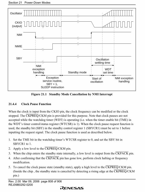
Section 21 Power-Down Modes
Rev. 2.00 Mar 09, 2006 page 808 of 906REJ09B0292-0200
Oscillator
CKIO(output)
NMI
NMIE
SBY Oscillationsettling time
Standby mode
Start ofoscillation
WDTset time
NMI exceptionhandling
Exceptionservice routine,
SBY = 1, SLEEP instruction
NMIexceptionhandling
Figure 21.1 Standby Mode Cancellation by NMI Interrupt
21.4.4 Clock Pause Function
When the clock is input from the CKIO pin, the clock frequency can be modified or the clockstopped. The CKPREQ/CKM pin is provided for this purpose. Note that clock pauses are notaccepted while the watchdog timer (WDT) is operating (i.e. when the timer enable bit (TME) inthe WDT�s timer control/status register (WTCSR) is 1). When the clock pause request function isused, the standby bit (SBY) in the standby control register 1 (SBYCR1) must be set to 1 beforeinputting the request signal. The clock pause function is used as described below.
1. Set the TME bit in the watchdog timer�s WTCSR register to 0, and set the SBY bit inSBYCR1 to 1.
2. Apply a low level to the CKPREQ/CKM pin.3. When the chip enters the standby state internally, a low level is output from the CKPACK pin.4. After confirming that the CKPACK pin has gone low, perform clock halting or frequency
modification.5. To cancel the clock pause state (standby state), apply a high level to the CKPREQ/CKM pin.
(Inside the chip , the standby state is canceled by detecting a rising edge at the CKPREQ/CKMpin.)
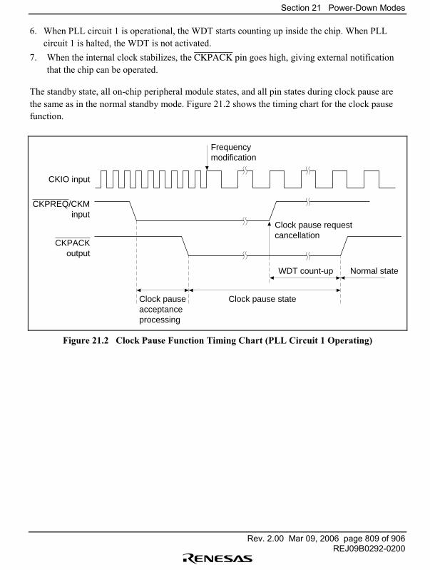
Section 21 Power-Down Modes
Rev. 2.00 Mar 09, 2006 page 809 of 906REJ09B0292-0200
6. When PLL circuit 1 is operational, the WDT starts counting up inside the chip. When PLLcircuit 1 is halted, the WDT is not activated.
7. When the internal clock stabilizes, the CKPACK pin goes high, giving external notificationthat the chip can be operated.
The standby state, all on-chip peripheral module states, and all pin states during clock pause arethe same as in the normal standby mode. Figure 21.2 shows the timing chart for the clock pausefunction.
CKIO input
CKPREQ/CKMinput
CKPACKoutput
Frequency modification
Clock pause request cancellation
Clock pause acceptance processing
WDT count-up Normal state
Clock pause state
Figure 21.2 Clock Pause Function Timing Chart (PLL Circuit 1 Operating)
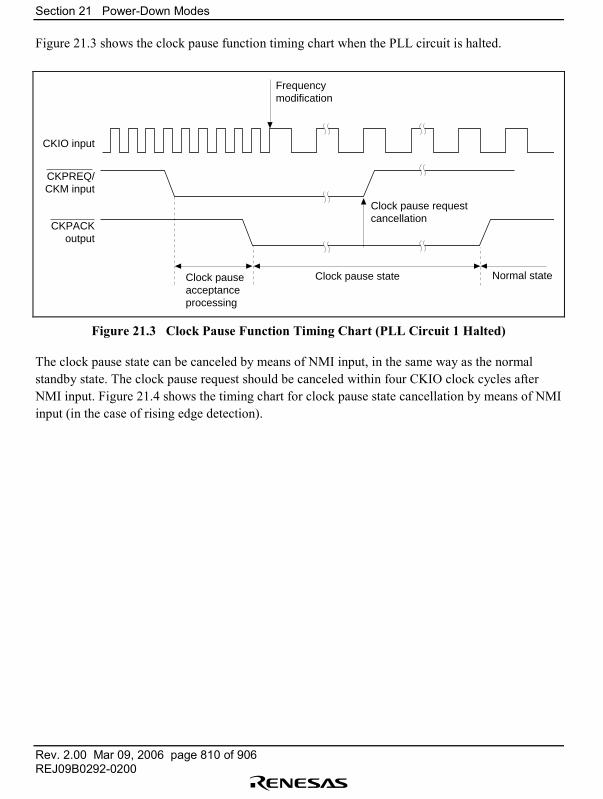
Section 21 Power-Down Modes
Rev. 2.00 Mar 09, 2006 page 810 of 906REJ09B0292-0200
Figure 21.3 shows the clock pause function timing chart when the PLL circuit is halted.
CKIO input
CKPREQ/CKM input
CKPACKoutput
Frequency modification
Clock pause request cancellation
Clock pause acceptance processing
Normal stateClock pause state
Figure 21.3 Clock Pause Function Timing Chart (PLL Circuit 1 Halted)
The clock pause state can be canceled by means of NMI input, in the same way as the normalstandby state. The clock pause request should be canceled within four CKIO clock cycles afterNMI input. Figure 21.4 shows the timing chart for clock pause state cancellation by means of NMIinput (in the case of rising edge detection).
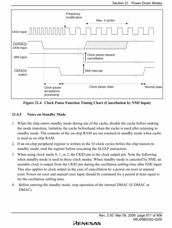
Section 21 Power-Down Modes
Rev. 2.00 Mar 09, 2006 page 811 of 906REJ09B0292-0200
CKIO input
CKPREQ/CKM input
CKPACKoutput
Frequency modification
Clock pause request cancellation
Clock pause acceptance processing
Normal stateClock pause state
Max. 4 cycles
NMI interrupt
NMI input
Figure 21.4 Clock Pause Function Timing Chart (Cancellation by NMI Input)
21.4.5 Notes on Standby Mode
1. When the chip enters standby mode during use of the cache, disable the cache before makingthe mode transition. Initialize the cache beforehand when the cache is used after returning tostandby mode. The contents of the on-chip RAM are not retained in standby mode when cacheis used as on-chip RAM.
2. If an on-chip peripheral register is written in the 10 clock cycles before the chip transits tostandby mode, read the register before executing the SLEEP instruction.
3. When using clock mode 0, 1, or 2, the CKIO pin is the clock output pin. Note the followingwhen standby mode is used in these clock modes. When standby mode is canceled by NMI, anunstable clock is output from the CKIO pin during the oscillation settling time after NMI input.This also applies to clock output in the case of cancellation by a power-on reset or manualreset. Power-on reset and manual reset input should be continued for a period at least equal tofor the oscillation settling time.
4. Before entering the standby mode, stop operation of the internal DMAC (E-DMAC orDMAC).
Section 21 Power-Down Modes
Rev. 2.00 Mar 09, 2006 page 812 of 906REJ09B0292-0200
21.5 Module Standby Function
21.5.1 Transition to Module Standby Function
By setting one of bits MSTP11�MSTP3, MSTP1 to 1 in standby control register 1 or 2, the supplyof the clock to the corresponding on-chip peripheral module or DSP unit can be halted. Thisfunction can be used to reduce the power consumption. Do not perform read/write operations for amodule in module standby mode.
With the module standby function, the external pins of the DMAC and SIO0�SIO2 on-chipperipheral modules retain their states prior to halting, as do DMAC, DSP, and SIO0�SIO2registers. The external pins of the FRT, SCIF1�2, and TPU are reset and all their registers areinitialized.
An on-chip peripheral module corresponding to a module standby bit must not be switched to themodule standby state while it is running. Also, interrupts from a module placed in the module stopstate should be disabled.
21.5.2 Clearing the Module Standby Function
Clear the module standby function by clearing the MSTP11�MSTP3, MSTP1 bits, or by a power-on reset or manual reset.

Section 22 Electrical Characteristics
Rev. 2.00 Mar 09, 2006 page 813 of 906REJ09B0292-0200
Section 22 Electrical Characteristics
22.1 Absolute Maximum Ratings
Table 22.1 shows the absolute maximum ratings.
Table 22.1 Absolute Maximum Ratings
Item Symbol Value Unit
Power supply voltage (internal) VCC �0.3 to +4.2 V
Power supply voltage (5 V I/O) PVCC �0.3 to +7.0 V
Input voltage (excluding 5 V I/O) Vin �0.3 to Vcc +0.3 V
Input voltage (5 V I/O) Vin �0.3 to PVcc +0.3 V
Operating temperature Topr �20 to +75 °C
Storage temperature Tstg �55 to +125 °CNotes: 1. Permanent damage to the chip may result if the maximum ratings are exceeded.
2. When powering on, turn on the 5 V I/O power supply (PVCC) after, or at the same timeas, the internal power supply (VCC). When powering off, cut Vcc after, or at the sametime as, PVCC.
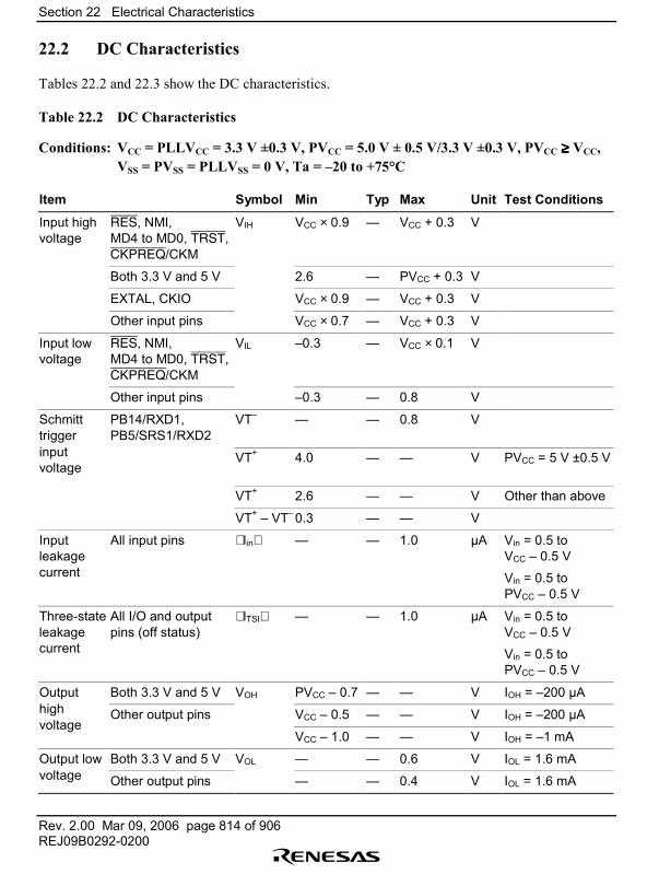
Section 22 Electrical Characteristics
Rev. 2.00 Mar 09, 2006 page 814 of 906REJ09B0292-0200
22.2 DC Characteristics
Tables 22.2 and 22.3 show the DC characteristics.
Table 22.2 DC Characteristics
Conditions: VCC = PLLVCC = 3.3 V ±0.3 V, PVCC = 5.0 V ± 0.5 V/3.3 V ±0.3 V, PVCC ≥≥≥≥ VCC,VSS = PVSS = PLLVSS = 0 V, Ta = �20 to +75°C
Item Symbol Min Typ Max Unit Test Conditions
Input highvoltage
RES, NMI,MD4 to MD0, TRST,CKPREQ/CKM
VIH VCC × 0.9 � VCC + 0.3 V
Both 3.3 V and 5 V 2.6 � PVCC + 0.3 V
EXTAL, CKIO VCC × 0.9 � VCC + 0.3 V
Other input pins VCC × 0.7 � VCC + 0.3 V
Input lowvoltage
RES, NMI,MD4 to MD0, TRST,CKPREQ/CKM
VIL �0.3 � VCC × 0.1 V
Other input pins �0.3 � 0.8 V
Schmitttrigger
PB14/RXD1,PB5/SRS1/RXD2
VT� � � 0.8 V
inputvoltage
VT+ 4.0 � � V PVCC = 5 V ±0.5 V
VT+ 2.6 � � V Other than above
VT+ � VT� 0.3 � � V
Inputleakagecurrent
All input pins lin � � 1.0 µA Vin = 0.5 toVCC � 0.5 V
Vin = 0.5 toPVCC � 0.5 V
Three-stateleakagecurrent
All I/O and outputpins (off status)
lTSI � � 1.0 µA Vin = 0.5 toVCC � 0.5 V
Vin = 0.5 toPVCC � 0.5 V
Output Both 3.3 V and 5 V VOH PVCC � 0.7 � � V IOH = �200 µAhigh Other output pins VCC � 0.5 � � V IOH = �200 µAvoltage
VCC � 1.0 � � V IOH = �1 mA
Output low Both 3.3 V and 5 V VOL � � 0.6 V IOL = 1.6 mAvoltage Other output pins � � 0.4 V IOL = 1.6 mA
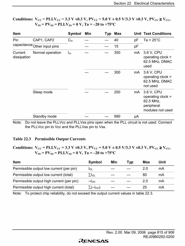
Section 22 Electrical Characteristics
Rev. 2.00 Mar 09, 2006 page 815 of 906REJ09B0292-0200
Conditions: VCC = PLLVCC = 3.3 V ±0.3 V, PVCC = 5.0 V ± 0.5 V/3.3 V ±0.3 V, PVCC ≥≥≥≥ VCC,VSS = PVSS = PLLVSS = 0 V, Ta = �20 to +75°C
Item Symbol Min Typ Max Unit Test Conditions
Pin CAP1, CAP2 Cin � � 40 pF Ta = 25°CcapacitanceOther input pins � � 15 pF
Currentdissipation
Normal operation lcc � � 350 mA 3.6 V, CPUoperating clock =62.5 MHz, DMACused
� � 300 mA 3.6 V, CPUoperating clock =62.5 MHz, DMACnot used
Sleep mode � � 250 mA 3.6 V, CPUoperating clock =62.5 MHz,peripheralmodules not used
Standby mode � � 990 µANote: Do not leave the PLLVcc and PLLVss pins open when the PLL circuit is not used. Connect
the PLLVcc pin to Vcc and the PLLVss pin to Vss.
Table 22.3 Permissible Output Currents
Conditions: VCC = PLLVCC = 3.3 V ±0.3 V, PVCC = 5.0 V ± 0.5 V/3.3 V ±0.3 V, PVCC ≥≥≥≥ VCC,VSS = PVSS = PLLVSS = 0 V, Ta = �20 to +75°C
Item Symbol Min Typ Max Unit
Permissible output low current (per pin) IOL � � 2.0 mA
Permissible output low current (total) ∑IOL � � 80 mA
Permissible output high current (per pin) �IOH � � 2.0 mA
Permissible output high current (total) ∑(�IOH) � � 25 mANote: To protect chip reliability, do not exceed the output current values in table 22.3.
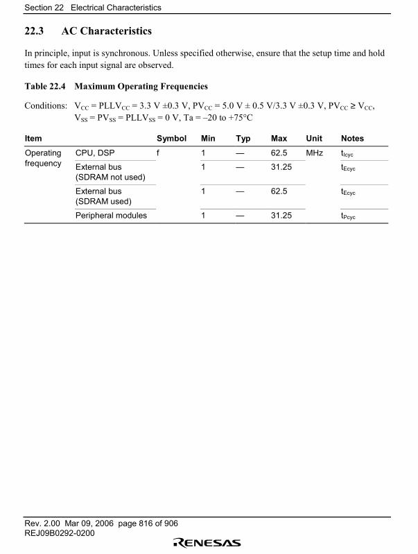
Section 22 Electrical Characteristics
Rev. 2.00 Mar 09, 2006 page 816 of 906REJ09B0292-0200
22.3 AC Characteristics
In principle, input is synchronous. Unless specified otherwise, ensure that the setup time and holdtimes for each input signal are observed.
Table 22.4 Maximum Operating Frequencies
Conditions: VCC = PLLVCC = 3.3 V ±0.3 V, PVCC = 5.0 V ± 0.5 V/3.3 V ±0.3 V, PVCC ≥ VCC,VSS = PVSS = PLLVSS = 0 V, Ta = �20 to +75°C
Item Symbol Min Typ Max Unit Notes
Operating CPU, DSP f 1 � 62.5 MHz tIcyc
frequency External bus(SDRAM not used)
1 � 31.25 tEcyc
External bus(SDRAM used)
1 � 62.5 tEcyc
Peripheral modules 1 � 31.25 tPcyc
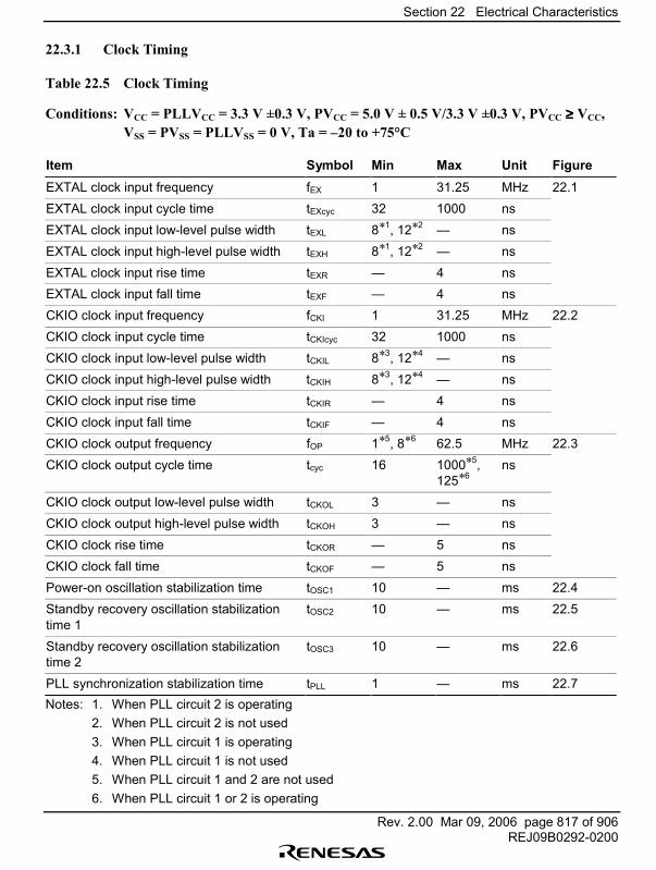
Section 22 Electrical Characteristics
Rev. 2.00 Mar 09, 2006 page 817 of 906REJ09B0292-0200
22.3.1 Clock Timing
Table 22.5 Clock Timing
Conditions: VCC = PLLVCC = 3.3 V ±0.3 V, PVCC = 5.0 V ± 0.5 V/3.3 V ±0.3 V, PVCC ≥≥≥≥ VCC,VSS = PVSS = PLLVSS = 0 V, Ta = �20 to +75°C
Item Symbol Min Max Unit FigureEXTAL clock input frequency fEX 1 31.25 MHz 22.1EXTAL clock input cycle time tEXcyc 32 1000 nsEXTAL clock input low-level pulse width tEXL 8*1, 12*2 � nsEXTAL clock input high-level pulse width tEXH 8*1, 12*2 � nsEXTAL clock input rise time tEXR � 4 nsEXTAL clock input fall time tEXF � 4 nsCKIO clock input frequency fCKI 1 31.25 MHz 22.2CKIO clock input cycle time tCKIcyc 32 1000 nsCKIO clock input low-level pulse width tCKIL 8*3, 12*4 � nsCKIO clock input high-level pulse width tCKIH 8*3, 12*4 � nsCKIO clock input rise time tCKIR � 4 nsCKIO clock input fall time tCKIF � 4 nsCKIO clock output frequency fOP 1*5, 8*6 62.5 MHz 22.3CKIO clock output cycle time tcyc 16 1000*5,
125*6ns
CKIO clock output low-level pulse width tCKOL 3 � nsCKIO clock output high-level pulse width tCKOH 3 � nsCKIO clock rise time tCKOR � 5 nsCKIO clock fall time tCKOF � 5 nsPower-on oscillation stabilization time tOSC1 10 � ms 22.4Standby recovery oscillation stabilizationtime 1
tOSC2 10 � ms 22.5
Standby recovery oscillation stabilizationtime 2
tOSC3 10 � ms 22.6
PLL synchronization stabilization time tPLL 1 � ms 22.7Notes: 1. When PLL circuit 2 is operating
2. When PLL circuit 2 is not used3. When PLL circuit 1 is operating4. When PLL circuit 1 is not used5. When PLL circuit 1 and 2 are not used6. When PLL circuit 1 or 2 is operating
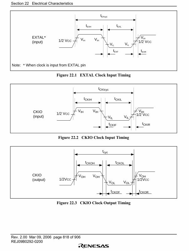
Section 22 Electrical Characteristics
Rev. 2.00 Mar 09, 2006 page 818 of 906REJ09B0292-0200
tEXH
tEXF tEXR
tEXL
tEXcyc
VIH VIHVIH
1/2 VCC 1/2 VCCVIL VIL
EXTAL*(input)
Note: * When clock is input from EXTAL pin
Figure 22.1 EXTAL Clock Input Timing
tCKIH
tCKIF tCKIR
tCKIL
tCKIcyc
VIH1/2 VCC 1/2 VCCVIH
VIL
VIH
VIL
CKIO(input)
Figure 22.2 CKIO Clock Input Timing
tcyc
tCKOLtCKOH
VOH1/2VCC
CKIO(output) 1/2VCC
tCKORtCKOF
VOH
VOL VOL
VOH
Figure 22.3 CKIO Clock Output Timing
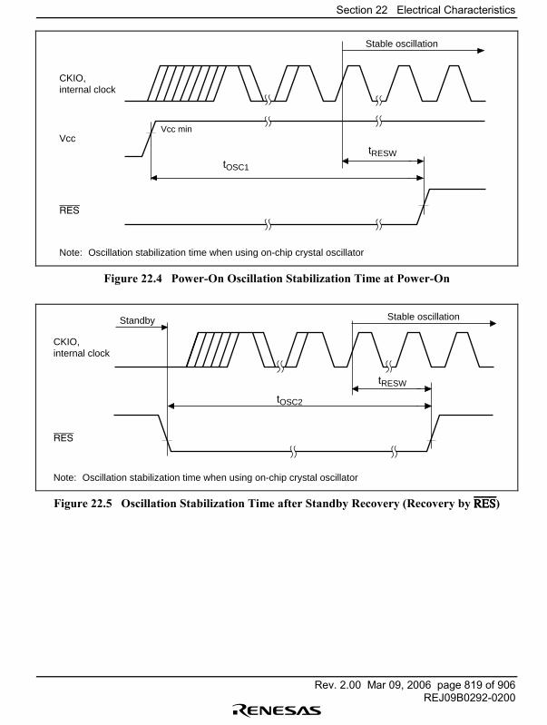
Section 22 Electrical Characteristics
Rev. 2.00 Mar 09, 2006 page 819 of 906REJ09B0292-0200
CKIO,internal clock
VccVcc min
RES
tOSC1
tRESW
Stable oscillation
Note: Oscillation stabilization time when using on-chip crystal oscillator
Figure 22.4 Power-On Oscillation Stabilization Time at Power-On
CKIO,internal clock
Stable oscillationStandby
tOSC2
tRESW
RES
Note: Oscillation stabilization time when using on-chip crystal oscillator
Figure 22.5 Oscillation Stabilization Time after Standby Recovery (Recovery by RESRESRESRES)
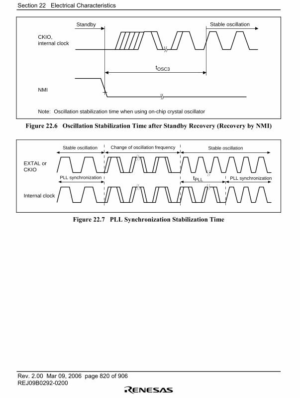
Section 22 Electrical Characteristics
Rev. 2.00 Mar 09, 2006 page 820 of 906REJ09B0292-0200
tOSC3
Stable oscillationStandby
CKIO,internal clock
NMI
Note: Oscillation stabilization time when using on-chip crystal oscillator
Figure 22.6 Oscillation Stabilization Time after Standby Recovery (Recovery by NMI)
tPLL
EXTAL orCKIO
Stable oscillation Stable oscillationChange of oscillation frequency
PLL synchronization PLL synchronization
Internal clock
Figure 22.7 PLL Synchronization Stabilization Time
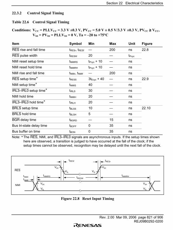
Section 22 Electrical Characteristics
Rev. 2.00 Mar 09, 2006 page 821 of 906REJ09B0292-0200
22.3.2 Control Signal Timing
Table 22.6 Control Signal Timing
Conditions: VCC = PLLVCC = 3.3 V ±0.3 V, PVCC = 5.0 V ± 0.5 V/3.3 V ±0.3 V, PVCC ≥≥≥≥ VCC,VSS = PVSS = PLLVSS = 0 V, Ta = �20 to +75°C
Item Symbol Min Max Unit Figure
RES rise and fall time tRESr, tRESf � 200 ns 22.8
RES pulse width tRESW 20 � tPcyc
NMI reset setup time tNMIRS tPcyc + 10 � ns
NMI reset hold time tNMIRH tPcyc + 10 � ns
NMI rise and fall time tNMIr, tNMIf � 200 ns
RES setup time* tRESS 3tEcyc + 40 � ns 22.9
NMI setup time* tNMIS 40 � ns
IRL3�IRL0 setup time* tIRLS 30 � ns
NMI hold time tNMIH 20 � ns
IRL3�IRL0 hold time* tIRLH 20 � ns
BRLS setup time tBLSS 10 � ns 22.10
BRLS hold time tBLSH 5 � ns
BGR delay time tBGRD � 15 ns
Bus tri-state delay time tBOFF 0 35 ns
Bus buffer on time tBON 0 35 nsNote: * The RES, NMI, and IRL3�IRL0 signals are asynchronous inputs. If the setup times shown
here are observed, a transition is judged to have occurred at the fall of the clock; if thesetup times cannot be observed, recognition may be delayed until the next fall of the clock.
tNMIRStNMIrtNMIf
tRESW
tRESf tRESr
tNMIRH
RES
NMI VIH
VIL
VIH
VIL
VIH VIH
VIL VIL
Figure 22.8 Reset Input Timing
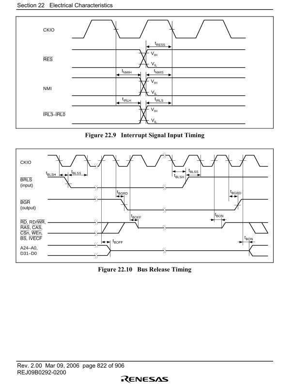
Section 22 Electrical Characteristics
Rev. 2.00 Mar 09, 2006 page 822 of 906REJ09B0292-0200
tRESS
CKIO
RES
tNMIS
NMI
tIRLS
IRL3–IRL0
tNMIH
tIRLH
VIH
VIL
VIH
VIL
VIH
VIL
Figure 22.9 Interrupt Signal Input Timing
A24–A0,D31–D0
RD, RD/WR,RAS, CAS,CSn, WEn,BS, IVECF
BRLS
(input)
BGR
(output)
tBLSS
CKIO
tBOFFtBON
tBONtBOFF
tBGRD tBGRD
tBLSHtBLSS
tBLSH
Figure 22.10 Bus Release Timing
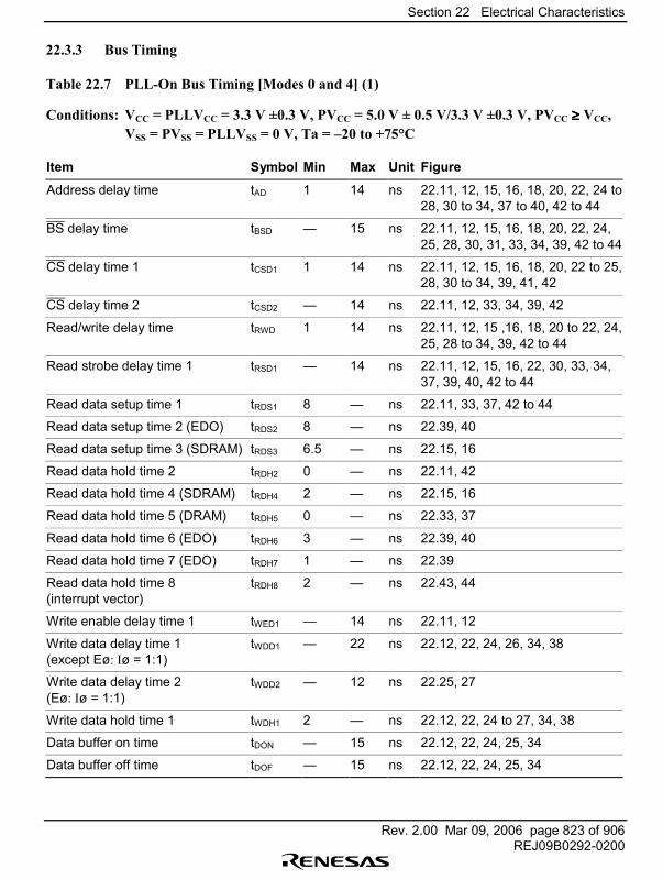
Section 22 Electrical Characteristics
Rev. 2.00 Mar 09, 2006 page 823 of 906REJ09B0292-0200
22.3.3 Bus Timing
Table 22.7 PLL-On Bus Timing [Modes 0 and 4] (1)
Conditions: VCC = PLLVCC = 3.3 V ±0.3 V, PVCC = 5.0 V ± 0.5 V/3.3 V ±0.3 V, PVCC ≥≥≥≥ VCC,VSS = PVSS = PLLVSS = 0 V, Ta = �20 to +75°C
Item Symbol Min Max Unit Figure
Address delay time tAD 1 14 ns 22.11, 12, 15, 16, 18, 20, 22, 24 to28, 30 to 34, 37 to 40, 42 to 44
BS delay time tBSD � 15 ns 22.11, 12, 15, 16, 18, 20, 22, 24,25, 28, 30, 31, 33, 34, 39, 42 to 44
CS delay time 1 tCSD1 1 14 ns 22.11, 12, 15, 16, 18, 20, 22 to 25,28, 30 to 34, 39, 41, 42
CS delay time 2 tCSD2 � 14 ns 22.11, 12, 33, 34, 39, 42
Read/write delay time tRWD 1 14 ns 22.11, 12, 15 ,16, 18, 20 to 22, 24,25, 28 to 34, 39, 42 to 44
Read strobe delay time 1 tRSD1 � 14 ns 22.11, 12, 15, 16, 22, 30, 33, 34,37, 39, 40, 42 to 44
Read data setup time 1 tRDS1 8 � ns 22.11, 33, 37, 42 to 44
Read data setup time 2 (EDO) tRDS2 8 � ns 22.39, 40
Read data setup time 3 (SDRAM) tRDS3 6.5 � ns 22.15, 16
Read data hold time 2 tRDH2 0 � ns 22.11, 42
Read data hold time 4 (SDRAM) tRDH4 2 � ns 22.15, 16
Read data hold time 5 (DRAM) tRDH5 0 � ns 22.33, 37
Read data hold time 6 (EDO) tRDH6 3 � ns 22.39, 40
Read data hold time 7 (EDO) tRDH7 1 � ns 22.39
Read data hold time 8(interrupt vector)
tRDH8 2 � ns 22.43, 44
Write enable delay time 1 tWED1 � 14 ns 22.11, 12
Write data delay time 1(except Eø: Iø = 1:1)
tWDD1 � 22 ns 22.12, 22, 24, 26, 34, 38
Write data delay time 2(Eø: Iø = 1:1)
tWDD2 � 12 ns 22.25, 27
Write data hold time 1 tWDH1 2 � ns 22.12, 22, 24 to 27, 34, 38
Data buffer on time tDON � 15 ns 22.12, 22, 24, 25, 34
Data buffer off time tDOF � 15 ns 22.12, 22, 24, 25, 34
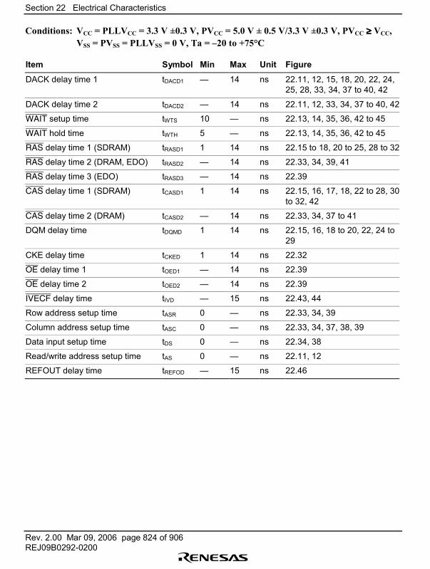
Section 22 Electrical Characteristics
Rev. 2.00 Mar 09, 2006 page 824 of 906REJ09B0292-0200
Conditions: VCC = PLLVCC = 3.3 V ±0.3 V, PVCC = 5.0 V ± 0.5 V/3.3 V ±0.3 V, PVCC ≥≥≥≥ VCC,VSS = PVSS = PLLVSS = 0 V, Ta = �20 to +75°C
Item Symbol Min Max Unit Figure
DACK delay time 1 tDACD1 � 14 ns 22.11, 12, 15, 18, 20, 22, 24,25, 28, 33, 34, 37 to 40, 42
DACK delay time 2 tDACD2 � 14 ns 22.11, 12, 33, 34, 37 to 40, 42
WAIT setup time tWTS 10 � ns 22.13, 14, 35, 36, 42 to 45
WAIT hold time tWTH 5 � ns 22.13, 14, 35, 36, 42 to 45
RAS delay time 1 (SDRAM) tRASD1 1 14 ns 22.15 to 18, 20 to 25, 28 to 32
RAS delay time 2 (DRAM, EDO) tRASD2 � 14 ns 22.33, 34, 39, 41
RAS delay time 3 (EDO) tRASD3 � 14 ns 22.39
CAS delay time 1 (SDRAM) tCASD1 1 14 ns 22.15, 16, 17, 18, 22 to 28, 30to 32, 42
CAS delay time 2 (DRAM) tCASD2 � 14 ns 22.33, 34, 37 to 41
DQM delay time tDQMD 1 14 ns 22.15, 16, 18 to 20, 22, 24 to29
CKE delay time tCKED 1 14 ns 22.32
OE delay time 1 tOED1 � 14 ns 22.39
OE delay time 2 tOED2 � 14 ns 22.39
IVECF delay time tIVD � 15 ns 22.43, 44
Row address setup time tASR 0 � ns 22.33, 34, 39
Column address setup time tASC 0 � ns 22.33, 34, 37, 38, 39
Data input setup time tDS 0 � ns 22.34, 38
Read/write address setup time tAS 0 � ns 22.11, 12
REFOUT delay time tREFOD � 15 ns 22.46
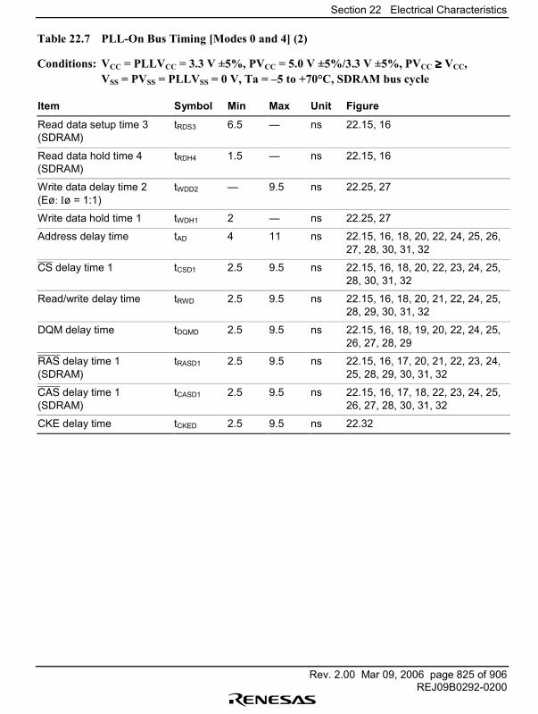
Section 22 Electrical Characteristics
Rev. 2.00 Mar 09, 2006 page 825 of 906REJ09B0292-0200
Table 22.7 PLL-On Bus Timing [Modes 0 and 4] (2)
Conditions: VCC = PLLVCC = 3.3 V ±5%, PVCC = 5.0 V ±5%/3.3 V ±5%, PVCC ≥≥≥≥ VCC,VSS = PVSS = PLLVSS = 0 V, Ta = �5 to +70°C, SDRAM bus cycle
Item Symbol Min Max Unit Figure
Read data setup time 3(SDRAM)
tRDS3 6.5 � ns 22.15, 16
Read data hold time 4(SDRAM)
tRDH4 1.5 � ns 22.15, 16
Write data delay time 2(Eø: Iø = 1:1)
tWDD2 � 9.5 ns 22.25, 27
Write data hold time 1 tWDH1 2 � ns 22.25, 27
Address delay time tAD 4 11 ns 22.15, 16, 18, 20, 22, 24, 25, 26,27, 28, 30, 31, 32
CS delay time 1 tCSD1 2.5 9.5 ns 22.15, 16, 18, 20, 22, 23, 24, 25,28, 30, 31, 32
Read/write delay time tRWD 2.5 9.5 ns 22.15, 16, 18, 20, 21, 22, 24, 25,28, 29, 30, 31, 32
DQM delay time tDQMD 2.5 9.5 ns 22.15, 16, 18, 19, 20, 22, 24, 25,26, 27, 28, 29
RAS delay time 1(SDRAM)
tRASD1 2.5 9.5 ns 22.15, 16, 17, 20, 21, 22, 23, 24,25, 28, 29, 30, 31, 32
CAS delay time 1(SDRAM)
tCASD1 2.5 9.5 ns 22.15, 16, 17, 18, 22, 23, 24, 25,26, 27, 28, 30, 31, 32
CKE delay time tCKED 2.5 9.5 ns 22.32
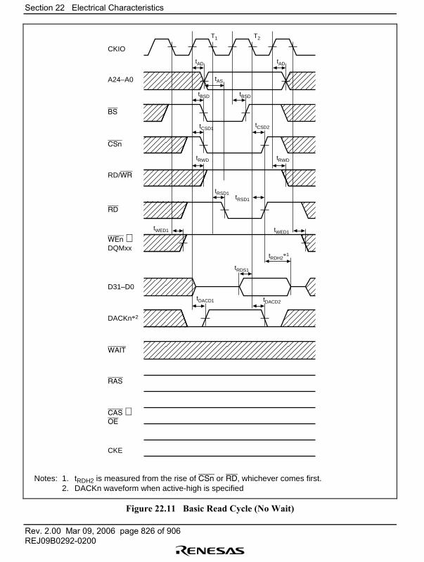
Section 22 Electrical Characteristics
Rev. 2.00 Mar 09, 2006 page 826 of 906REJ09B0292-0200
CKIO
BS
CSn
RD/WR
RD
WEn ⋅DQMxx
RAS
CAS ⋅OE
CKE
DACKn*2
WAIT
A24–A0
T1 T2
tAD
tAS
tBSD tBSD
tAD
tCSD1
tRWD tRWD
tWED1
tRDS1
tRDH2*1
tWED1
tCSD2
tRSD1tRSD1
tDACD1 tDACD2
D31–D0
Notes: 1. tRDH2 is measured from the rise of CSn or RD, whichever comes first. 2. DACKn waveform when active-high is specified
Figure 22.11 Basic Read Cycle (No Wait)
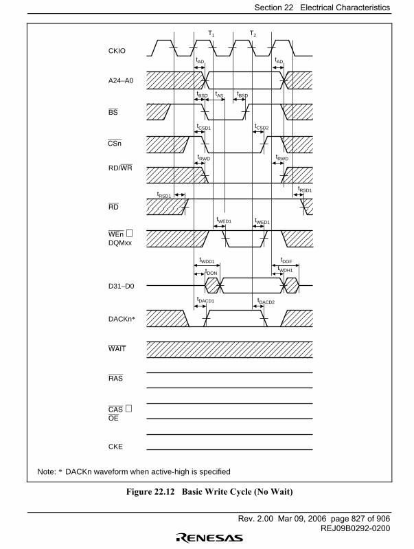
Section 22 Electrical Characteristics
Rev. 2.00 Mar 09, 2006 page 827 of 906REJ09B0292-0200
CKIO
BS
CSn
RD/WR
RD
WEn ⋅DQMxx
RAS
CAS ⋅OE
CKE
D31–D0
DACKn*
WAIT
A24–A0
T1 T2
tAD
tBSD tBSD
tAD
tCSD1
tRWD tRWD
tRSD1
tRSD1
tCSD2
tWED1 tWED1
tDACD1 tDACD2
tDONtWDH1
tWDD1 tDOF
Note: * DACKn waveform when active-high is specified
tAS
Figure 22.12 Basic Write Cycle (No Wait)
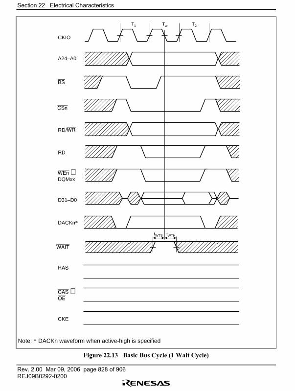
Section 22 Electrical Characteristics
Rev. 2.00 Mar 09, 2006 page 828 of 906REJ09B0292-0200
T1 Tw T2
CKIO
BS
CSn
RD/WR
RD
WEn ⋅DQMxx
RAS
CAS ⋅OE
CKE
D31–D0
DACKn*
WAIT
A24–A0
tWTHtWTS
Note: * DACKn waveform when active-high is specified
Figure 22.13 Basic Bus Cycle (1 Wait Cycle)
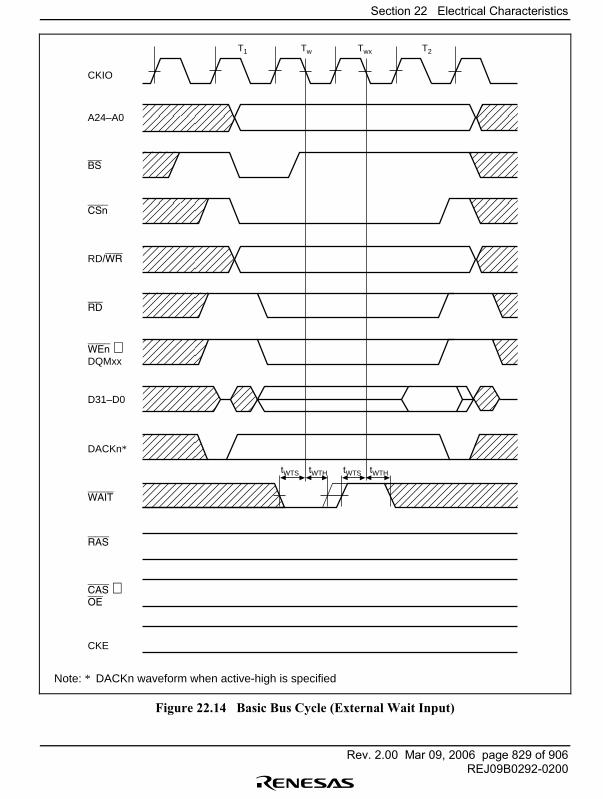
Section 22 Electrical Characteristics
Rev. 2.00 Mar 09, 2006 page 829 of 906REJ09B0292-0200
T1 Tw Twx T2
CKIO
BS
CSn
RD/WR
RD
WEn ⋅DQMxx
RAS
CAS ⋅OE
CKE
D31–D0
DACKn*
WAIT
A24–A0
tWTS tWTH tWTS tWTH
Note: * DACKn waveform when active-high is specified
Figure 22.14 Basic Bus Cycle (External Wait Input)
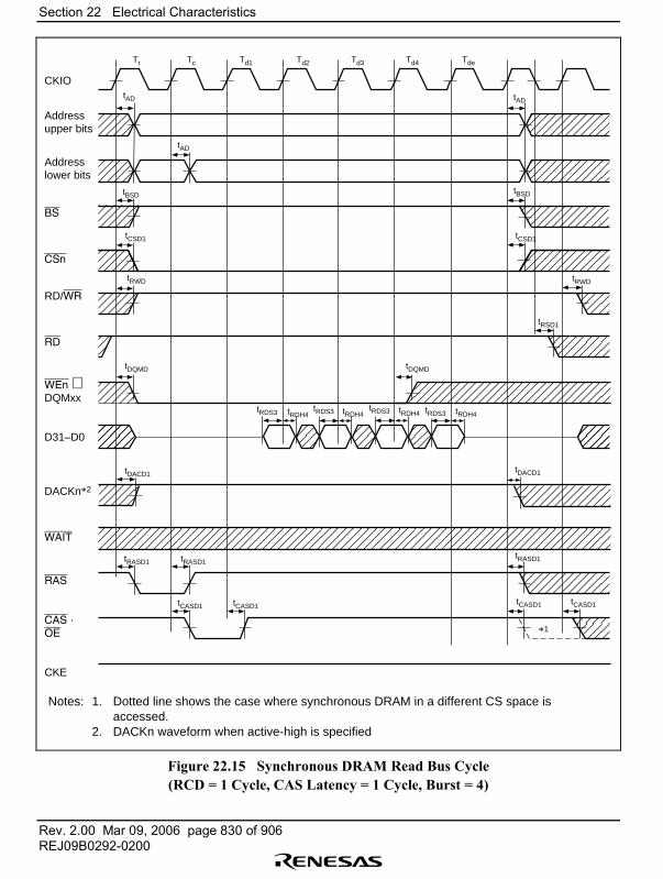
Section 22 Electrical Characteristics
Rev. 2.00 Mar 09, 2006 page 830 of 906REJ09B0292-0200
Tr Tc Td1 Td2 Td3 Td4 Tde
tAD
tAD
tBSD
tRWD
tCSD1
tDQMD
tRDS3 tRDH4 tRDS3tRDS3 tRDH4tRDS3 tRDH4
tDACD1
tRASD1 tRASD1
tCASD1 tCASD1
tDQMD
tRASD1
tDACD1
tCASD1tCASD1
*1
tRDH4
tRWD
tRSD1
tCSD1
tAD
tBSD
Notes: 1. Dotted line shows the case where synchronous DRAM in a different CS space is accessed. 2. DACKn waveform when active-high is specified
CKIO
BS
CSn
RD/WR
RD
WEn ⋅DQMxx
D31–D0
RAS
CAS · OE
CKE
DACKn*2
WAIT
Addressupper bits
Addresslower bits
Figure 22.15 Synchronous DRAM Read Bus Cycle(RCD = 1 Cycle, CAS Latency = 1 Cycle, Burst = 4)

Section 22 Electrical Characteristics
Rev. 2.00 Mar 09, 2006 page 831 of 906REJ09B0292-0200
Tr Tc Td1 Td2 Td3 Td4 Tde
tAD
tAD
tBSD
tRWD
tCSD1
tDQMD
tRDS3 tRDH4
tRASD1 tRASD1
tCASD1 tCASD1
tDQMD
Notes: 1. Dotted line shows the case where synchronous DRAM in a different CS space is accessed. 2. DACKn waveform when active-high is specified
CKIO
BS
CSn
RD/WR
RD
WEn ⋅DQMxx
RAS
CAS ⋅OE
CKE
D31–D0
WAIT
Addressupper bits
Addresslower bits
DACKn*2
tCASD1tCASD1
tRASD1
tDQMD
tRSD1
tRWD
tCSD1
tBSD
tAD
*1
Figure 22.16 Synchronous DRAM Single Read Bus Cycle(RCD = 1 Cycle, CAS Latency = 1 Cycle, Burst = 4)
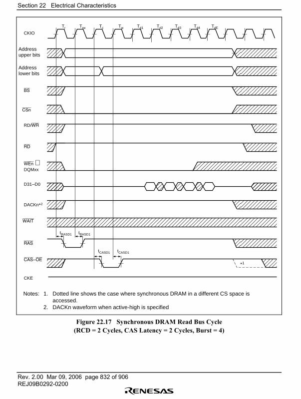
Section 22 Electrical Characteristics
Rev. 2.00 Mar 09, 2006 page 832 of 906REJ09B0292-0200
CKIO
BS
CSn
RD/WR
RD
WEn ⋅DQMxx
RAS
CAS–OE
CKE
D31–D0
*1
DACKn*2
WAIT
Tr Trw Tc Tw Td1 Td2 Td3 Td4 TdE
tRASD1
tCASD1 tCASD1
tRASD1
Addressupper bits
Addresslower bits
Notes: 1. Dotted line shows the case where synchronous DRAM in a different CS space is accessed. 2. DACKn waveform when active-high is specified
Figure 22.17 Synchronous DRAM Read Bus Cycle(RCD = 2 Cycles, CAS Latency = 2 Cycles, Burst = 4)
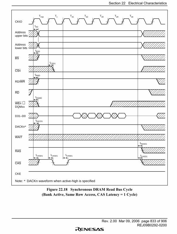
Section 22 Electrical Characteristics
Rev. 2.00 Mar 09, 2006 page 833 of 906REJ09B0292-0200
Tnop Tc Td1 Td2 Td3 Td4 Tde
tAD
tBSD
tRWD
tCSD1
tDQMD
tDACD1
tCASD1tCASD1 tCASD1 tCASD1
tRASD1
CKIO
BS
CSn
RD/WR
RD
WEn ⋅DQMxx
CAS
CKE
D31–D0
DACKn*
WAIT
RAS
Addressupper bits
Addresslower bits
Note: * DACKn waveform when active-high is specified
Figure 22.18 Synchronous DRAM Read Bus Cycle(Bank Active, Same Row Access, CAS Latency = 1 Cycle)
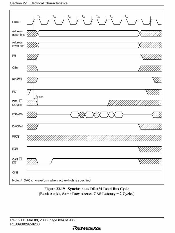
Section 22 Electrical Characteristics
Rev. 2.00 Mar 09, 2006 page 834 of 906REJ09B0292-0200
TC TW Td1 Td2 Td3 Td4 Tde
tDQMD
Addressupper bits
Addresslower bits
BS
CKIO
CSn
RD/WR
RD
WEn ⋅DQMxx
D31–D0
DACKn*
WAIT
RAS
CAS ⋅OE
CKE
Note: * DACKn waveform when active-high is specified
Figure 22.19 Synchronous DRAM Read Bus Cycle(Bank Active, Same Row Access, CAS Latency = 2 Cycles)
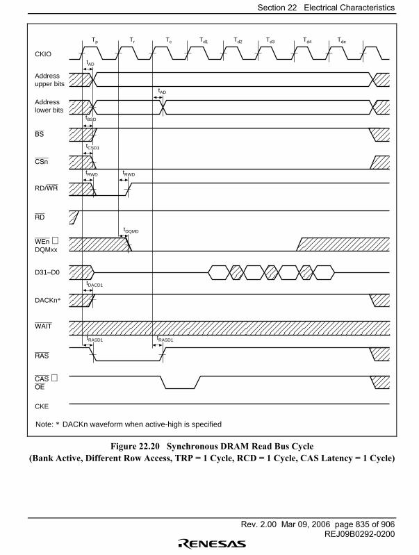
Section 22 Electrical Characteristics
Rev. 2.00 Mar 09, 2006 page 835 of 906REJ09B0292-0200
Tp Tr Tc Td1 Td2 Td3 TdeTd4
tAD
tAD
tRWD tRWD
tDACD1
tRASD1 tRASD1
tDQMD
tCSD1
tBSD
Addressupper bits
Addresslower bits
BS
CKIO
CSn
RD/WR
RD
WEn ⋅DQMxx
D31–D0
DACKn*
WAIT
RAS
CAS ⋅OE
CKE
Note: * DACKn waveform when active-high is specified
Figure 22.20 Synchronous DRAM Read Bus Cycle(Bank Active, Different Row Access, TRP = 1 Cycle, RCD = 1 Cycle, CAS Latency = 1 Cycle)
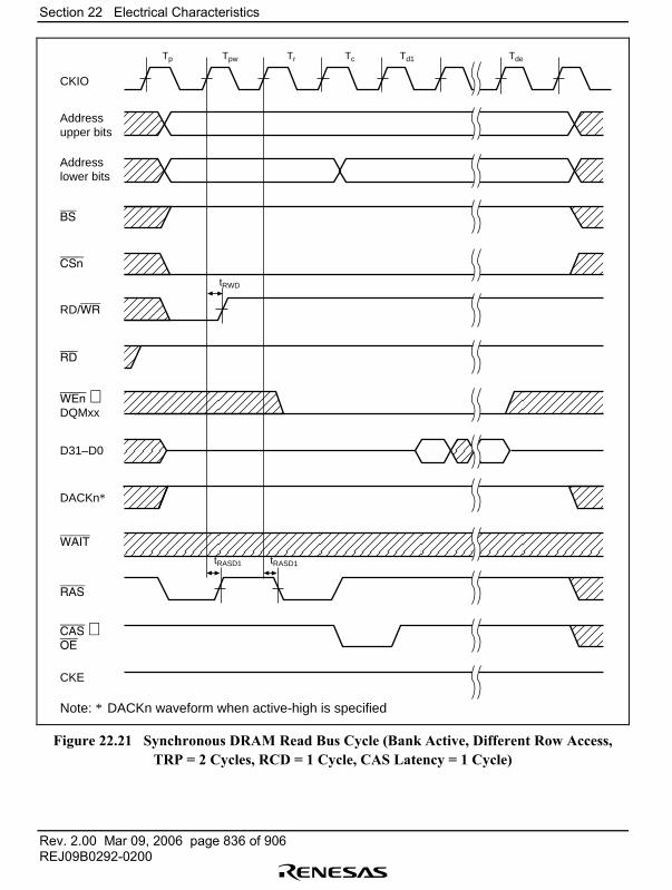
Section 22 Electrical Characteristics
Rev. 2.00 Mar 09, 2006 page 836 of 906REJ09B0292-0200
Addressupper bits
Addresslower bits
BS
CKIO
Tp Tpw Tr Tc Td1 Tde
CSn
RD/WR
RD
WEn ⋅DQMxx
D31–D0
DACKn*
WAIT
RAS
CAS ⋅OE
CKE
tRWD
tRASD1 tRASD1
Note: * DACKn waveform when active-high is specified
Figure 22.21 Synchronous DRAM Read Bus Cycle (Bank Active, Different Row Access,TRP = 2 Cycles, RCD = 1 Cycle, CAS Latency = 1 Cycle)
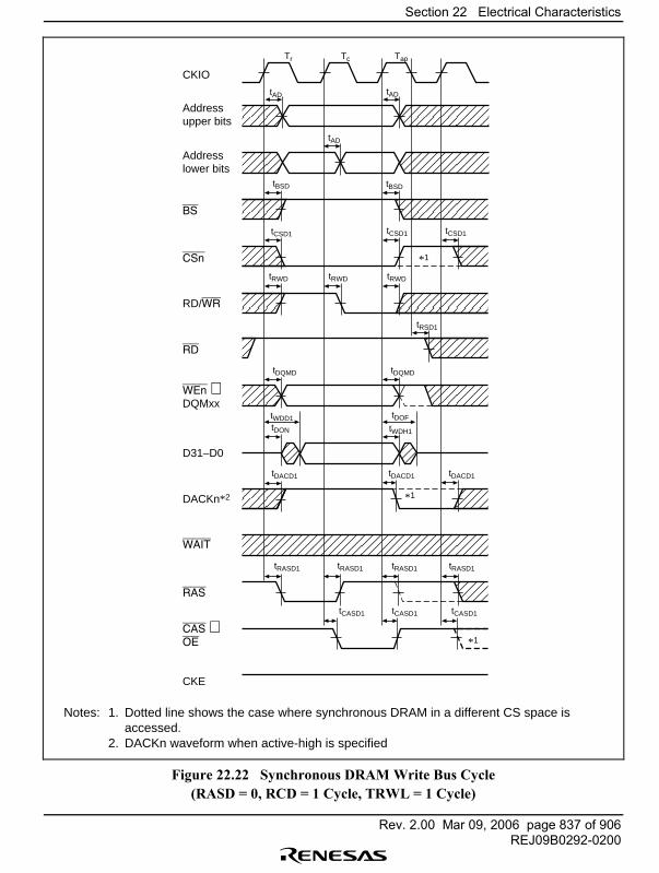
Section 22 Electrical Characteristics
Rev. 2.00 Mar 09, 2006 page 837 of 906REJ09B0292-0200
CKIO
Tr Tc Tap
Addressupper bits
WEn ⋅DQMxx
D31–D0
Addresslower bits
BS
CSn
RD
RD/WR
DACKn*2
WAIT
RAS
CAS ⋅OE
CKE
tAD tAD
tAD
tBSD
tCSD1
tRWD
tDQMD
tDACD1
tRASD1 tRASD1
tCASD1 tCASD1 tCASD1
tRASD1 tRASD1
tDQMD
tDOF
tDACD1tDACD1
tDON
tWDD1
tRWD tRWD
tRSD1
tCSD1 tCSD1
tBSD
tWDH1
Notes: 1. Dotted line shows the case where synchronous DRAM in a different CS space is accessed. 2. DACKn waveform when active-high is specified
*1
*1
*1
Figure 22.22 Synchronous DRAM Write Bus Cycle(RASD = 0, RCD = 1 Cycle, TRWL = 1 Cycle)

Section 22 Electrical Characteristics
Rev. 2.00 Mar 09, 2006 page 838 of 906REJ09B0292-0200
Tr Trw Tc Trwl Tap
CKIO
Addressupper bits
Addresslower bits
BS
CSn
RD/WR
RD
WEn ⋅DQMxx
D31–D0
DACKn*2
WAIT
RAS
CAS ⋅OE
CKE
tRASD1
tCASD1
tRASD1
tCSD1
Notes: 1. Dotted line shows the case where synchronous DRAM in a different CS space is accessed. 2. DACKn waveform when active-high is specified
*1
*1
Figure 22.23 Synchronous DRAM Write Bus Cycle(RASD = 0, RCD = 2 Cycles, TRWL = 2 Cycles)
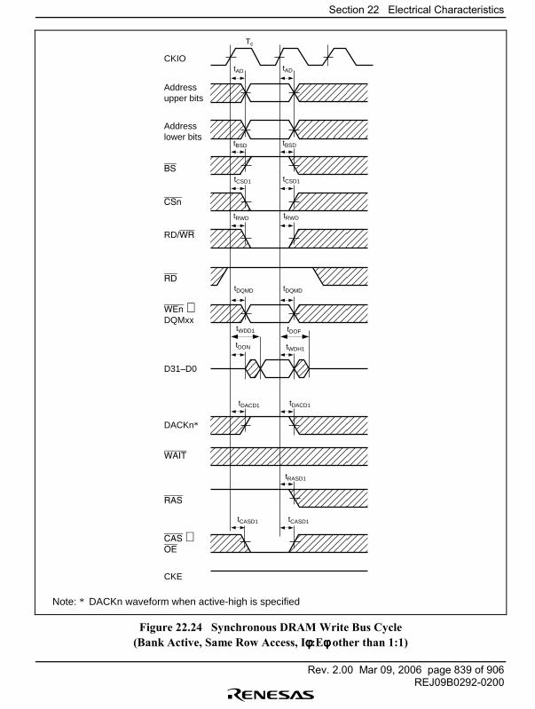
Section 22 Electrical Characteristics
Rev. 2.00 Mar 09, 2006 page 839 of 906REJ09B0292-0200
Tc
CKIO
Addressupper bits
Addresslower bits
BS
CSn
RD/WR
RD
WEn ⋅DQMxx
D31–D0
DACKn*
WAIT
RAS
CAS ⋅OE
CKE
tADtAD
tBSDtBSD
tCSD1 tCSD1
tRWD tRWD
tDQMD tDQMD
tWDD1 tDOF
tWDH1tDON
tDACD1tDACD1
tRASD1
tCASD1tCASD1
Note: * DACKn waveform when active-high is specified
Figure 22.24 Synchronous DRAM Write Bus Cycle(Bank Active, Same Row Access, Iφφφφ:Eφφφφ other than 1:1)
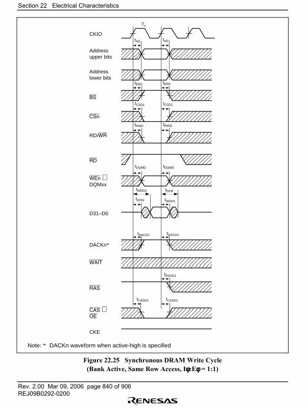
Section 22 Electrical Characteristics
Rev. 2.00 Mar 09, 2006 page 840 of 906REJ09B0292-0200
Tc
CKIO
Addressupper bits
Addresslower bits
BS
CSn
RD/WR
RD
WEn ⋅DQMxx
D31–D0
DACKn*
WAIT
RAS
CAS ⋅OE
CKE
tADtAD
tBSDtBSD
tCSD1 tCSD1
tRWD tRWD
tDQMD tDQMD
tWDD2 tDOF
tWDH1tDON
tDACD1tDACD1
tRASD1
tCASD1tCASD1
Note: * DACKn waveform when active-high is specified
Figure 22.25 Synchronous DRAM Write Cycle(Bank Active, Same Row Access, Iφφφφ:Eφφφφ = 1:1)
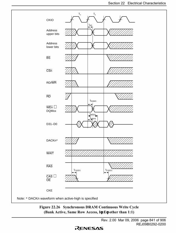
Section 22 Electrical Characteristics
Rev. 2.00 Mar 09, 2006 page 841 of 906REJ09B0292-0200
Tc
CKIO
Addressupper bits
Addresslower bits
BS
CSn
RD/WR
RD
WEn ⋅DQMxx
D31–D0
DACKn*
WAIT
RAS
CAS ⋅OE
CKE
tAD
Tc
tDQMD
tWDD1
tWDH1
tCASD1 tCASD1
Note: * DACKn waveform when active-high is specified
Figure 22.26 Synchronous DRAM Continuous Write Cycle(Bank Active, Same Row Access, Iφφφφ:Eφφφφ other than 1:1)
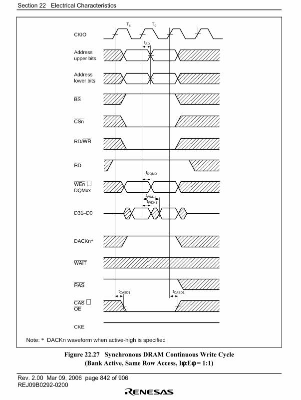
Section 22 Electrical Characteristics
Rev. 2.00 Mar 09, 2006 page 842 of 906REJ09B0292-0200
Tc
CKIO
Addressupper bits
Addresslower bits
BS
CSn
RD/WR
RD
WEn ⋅DQMxx
D31–D0
DACKn*
WAIT
RAS
CAS ⋅OE
CKE
tAD
Tc
tDQMD
tWDD2
tWDH1
tCASD1 tCASD1
Note: * DACKn waveform when active-high is specified
Figure 22.27 Synchronous DRAM Continuous Write Cycle(Bank Active, Same Row Access, Iφφφφ:Eφφφφ = 1:1)
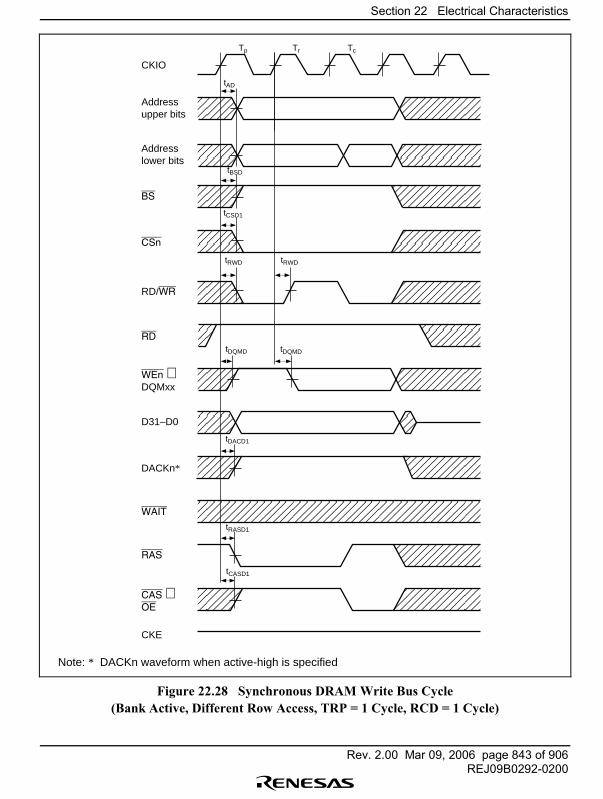
Section 22 Electrical Characteristics
Rev. 2.00 Mar 09, 2006 page 843 of 906REJ09B0292-0200
CKIO
Addressupper bits
Addresslower bits
BS
CSn
RD/WR
RD
WEn ⋅DQMxx
D31–D0
DACKn*
WAIT
RAS
CAS ⋅OE
CKE
tAD
Tp Tr Tc
tBSD
tCSD1
tRWD tRWD
tDQMD tDQMD
tDACD1
tRASD1
tCASD1
Note: * DACKn waveform when active-high is specified
Figure 22.28 Synchronous DRAM Write Bus Cycle(Bank Active, Different Row Access, TRP = 1 Cycle, RCD = 1 Cycle)
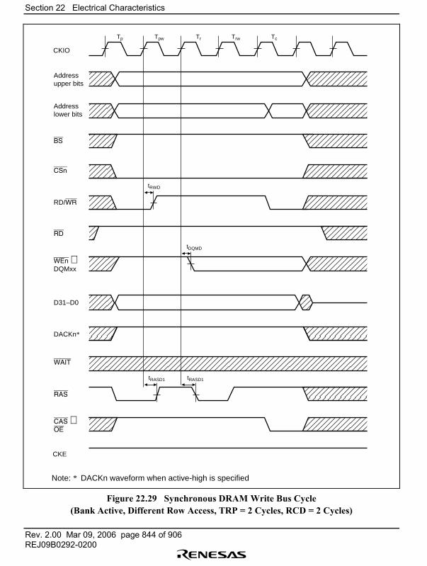
Section 22 Electrical Characteristics
Rev. 2.00 Mar 09, 2006 page 844 of 906REJ09B0292-0200
Addressupper bits
Addresslower bits
BS
CKIO
Tp Tpw Tr Trw Tc
CSn
RD/WR
RD
WEn ⋅DQMxx
D31–D0
DACKn*
WAIT
RAS
CAS ⋅OE
CKE
tRWD
tDQMD
tRASD1 tRASD1
Note: * DACKn waveform when active-high is specified
Figure 22.29 Synchronous DRAM Write Bus Cycle(Bank Active, Different Row Access, TRP = 2 Cycles, RCD = 2 Cycles)
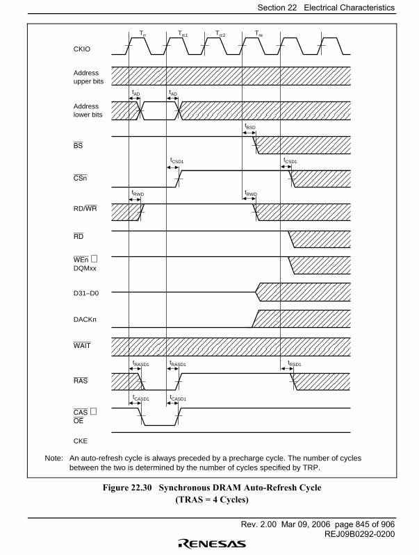
Section 22 Electrical Characteristics
Rev. 2.00 Mar 09, 2006 page 845 of 906REJ09B0292-0200
CKIO
BS
CSn
RD
RD/WR
WEn ⋅DQMxx
RAS
CAS ⋅OE
CKE
D31–D0
DACKn
WAIT
Address upper bits
Trr Trc1 TreTrc2
Address lower bits
tRASD1 tRSD1tRASD1
tCASD1 tCASD1
tAD tAD
tCSD1
tRWD tRWD
tBSD
tCSD1
Note: An auto-refresh cycle is always preceded by a precharge cycle. The number of cycles between the two is determined by the number of cycles specified by TRP.
Figure 22.30 Synchronous DRAM Auto-Refresh Cycle(TRAS = 4 Cycles)
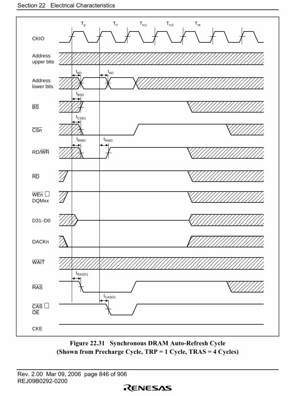
Section 22 Electrical Characteristics
Rev. 2.00 Mar 09, 2006 page 846 of 906REJ09B0292-0200
CKIO
BS
RD
CSn
RD/WR
WEn ⋅DQMxx
RAS
CAS ⋅OE
D31–D0
DACKn
WAIT
Address upper bits
Tp Trr Trc2 TreTrc1
Address lower bits
CKE
tRASD1
tCASD1
tAD tAD
tBSD
tCSD1
tRWD tRWD
Figure 22.31 Synchronous DRAM Auto-Refresh Cycle(Shown from Precharge Cycle, TRP = 1 Cycle, TRAS = 4 Cycles)
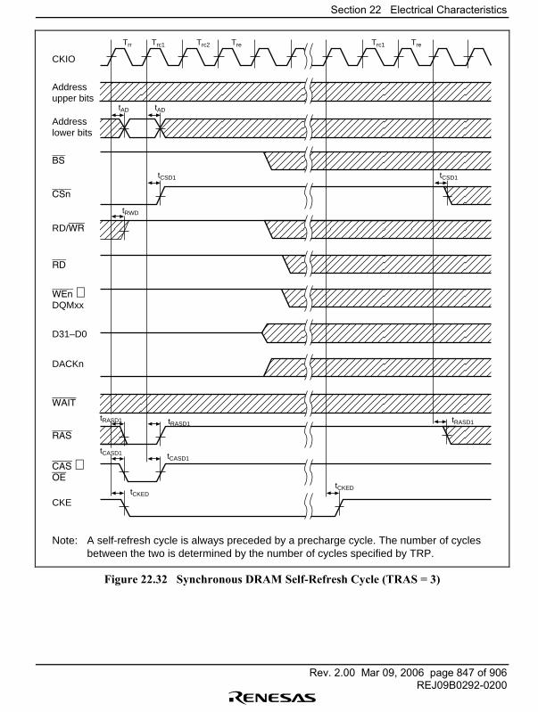
Section 22 Electrical Characteristics
Rev. 2.00 Mar 09, 2006 page 847 of 906REJ09B0292-0200
Address upper bits
Address lower bits
BS
CKIO
Trr Trc1 Trc2 Tre Trc1
CSn
RD/WR
WEn ⋅DQMxx
D31–D0
DACKn
RD
WAIT
RAS
CAS ⋅OE
CKE
tAD
tRWD
tAD
tRASD1
tCASD1
tCKEDtCKED
tRASD1
tCSD1 tCSD1
Tre
tRASD1
tCASD1
Note: A self-refresh cycle is always preceded by a precharge cycle. The number of cycles between the two is determined by the number of cycles specified by TRP.
Figure 22.32 Synchronous DRAM Self-Refresh Cycle (TRAS = 3)
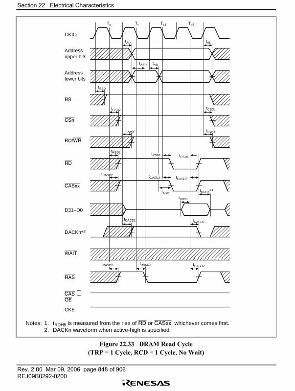
Section 22 Electrical Characteristics
Rev. 2.00 Mar 09, 2006 page 848 of 906REJ09B0292-0200
CKIO
Tp Tr Tc1 Tc2
tAD
tADtASR
tBSD
tRDS1
tDACD2
tAD
BS
CSn
RD/WR
RD
CASxx
RAS
CAS ⋅OE
CKE
D31–D0
DACKn*2
WAIT
Addressupper bits
Addresslower bits
tRSD1
tCASD2
tCSD2 tCSD1
tRWD tRWD
tRASD2tRASD2
tDACD1
tRSD1
tRDH5*1
tCASD2
tRASD2
Notes: 1. tRDH5 is measured from the rise of RD or CASxx, whichever comes first. 2. DACKn waveform when active-high is specified
tRSD1
tCASD2
tASC
Figure 22.33 DRAM Read Cycle(TRP = 1 Cycle, RCD = 1 Cycle, No Wait)
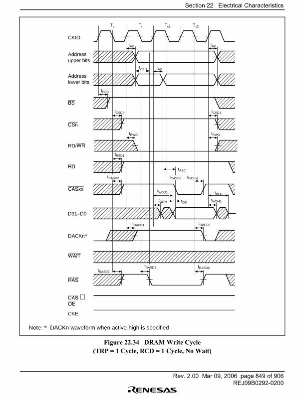
Section 22 Electrical Characteristics
Rev. 2.00 Mar 09, 2006 page 849 of 906REJ09B0292-0200
CKIO
Tp Tr Tc1 Tc2
tAD
tAD
tBSD
tDACD2
tAD
BS
CSn
RD/WR
RD
CASxx
RAS
CAS ⋅OE
CKE
D31–D0
DACKn*
WAIT
Addressupper bits
Addresslower bits
tCASD2
tCSD2 tCSD1
tRWD tRWD
tRASD2tRASD2tRASD2
tRSD1
tDON tWDH1
tDOF
tCASD2 tCASD2
tWDD1
tASC
tDS
tDACD1
Note: * DACKn waveform when active-high is specified
tASR
Figure 22.34 DRAM Write Cycle(TRP = 1 Cycle, RCD = 1 Cycle, No Wait)
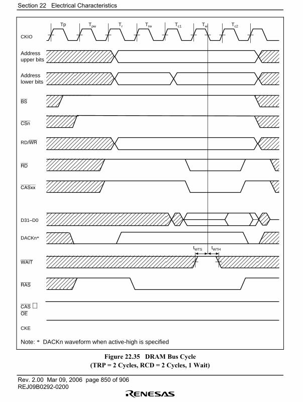
Section 22 Electrical Characteristics
Rev. 2.00 Mar 09, 2006 page 850 of 906REJ09B0292-0200
CKIO
BS
CSn
RD/WR
RD
CASxx
RAS
CAS ⋅OE
CKE
D31–D0
DACKn*
WAIT
Addressupper bits
Addresslower bits
Tp Tpw Tr Trw Tc1 Tc2Tw
tWTHtWTS
Note: * DACKn waveform when active-high is specified
Figure 22.35 DRAM Bus Cycle(TRP = 2 Cycles, RCD = 2 Cycles, 1 Wait)
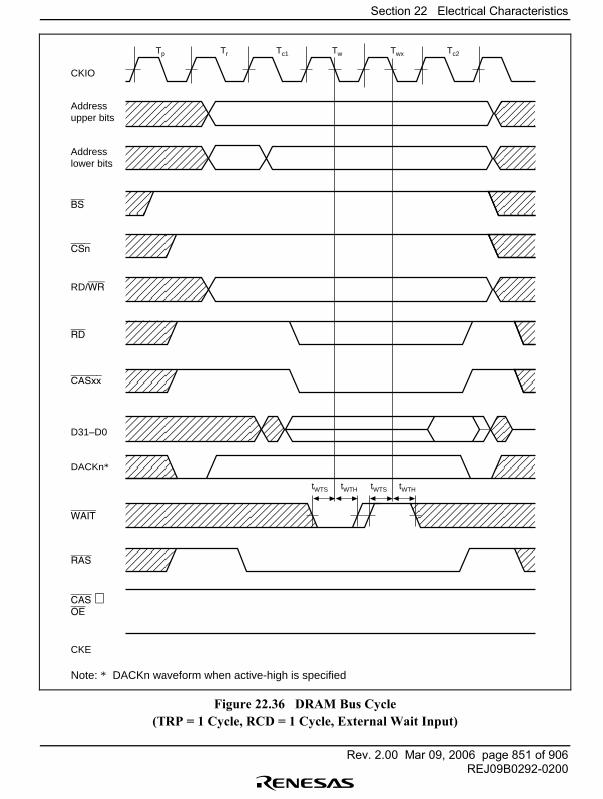
Section 22 Electrical Characteristics
Rev. 2.00 Mar 09, 2006 page 851 of 906REJ09B0292-0200
CKIO
Tp Tr Tc1 Tw Twx Tc2
BS
CSn
RD/WR
RD
CASxx
RAS
CAS ⋅OE
CKE
D31–D0
DACKn*
WAIT
Addressupper bits
Addresslower bits
tWTS tWTH tWTS tWTH
Note: * DACKn waveform when active-high is specified
Figure 22.36 DRAM Bus Cycle(TRP = 1 Cycle, RCD = 1 Cycle, External Wait Input)

Section 22 Electrical Characteristics
Rev. 2.00 Mar 09, 2006 page 852 of 906REJ09B0292-0200
CKIO
Tp Tr Tc1 Tc2 Tc1 Tc2
tADtAD
tDACD1
BS
RD/WR
RD
CASxx
RAS
CAS ⋅OE
CKE
D31–D0
DACKn*2
WAIT
Addressupper bits
Addresslower bits
tRSD1
tRSD1
tCASD2
tASC tASC
tCASD2
tDACD2
tRDS1
CSn
tRDH5*1
tRDS1
tRDH5*1
Notes: 1. tRDH5 is measured from the rise of RD or CASxx, whichever comes first. 2. DACKn waveform when active-high is specified
Figure 22.37 DRAM Burst Read Cycle(TRP = 1 Cycle, RCD = 1 Cycle, No Wait)
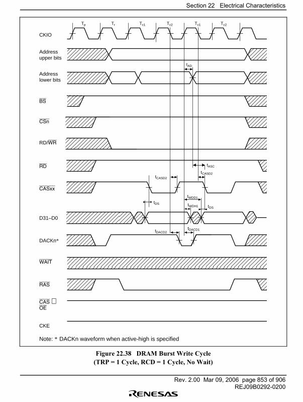
Section 22 Electrical Characteristics
Rev. 2.00 Mar 09, 2006 page 853 of 906REJ09B0292-0200
CKIO
Tp Tr Tc1 Tc2 Tc1 Tc2
tAD
tDACD1
BS
CSn
RD/WR
RD
CASxx
RAS
CAS ⋅OE
CKE
D31–D0
DACKn*
WAIT
Addressupper bits
Addresslower bits
tWDH1
tCASD2
tWDD1
tDACD2
Note: * DACKn waveform when active-high is specified
tCASD2
tASC
tDS
tDS
Figure 22.38 DRAM Burst Write Cycle(TRP = 1 Cycle, RCD = 1 Cycle, No Wait)
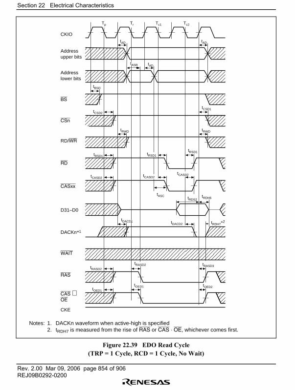
Section 22 Electrical Characteristics
Rev. 2.00 Mar 09, 2006 page 854 of 906REJ09B0292-0200
CKIO
Tp Tr Tc1 Tc2
tAD
tBSD
tRDS2
tDACD2 tRDH7*2
tAD
BS
CSn
RD/WR
RD
CASxx
RAS
CAS ⋅OE
CKE
D31–D0
DACKn*1
WAIT
Addressupper bits
Addresslower bits
tRSD1
tASC
tCSD2
tCSD1
tRWD tRWD
tCASD2
tRASD3tRASD2
tRASD2
tOED2tOED1tOED1
tRDH6
tRSD1
Notes: 1. DACKn waveform when active-high is specified 2. tRDH7 is measured from the rise of RAS or CAS · OE, whichever comes first.
tRSD1
tCASD2
tDACD1
tASR tAD
tCASD2
Figure 22.39 EDO Read Cycle(TRP = 1 Cycle, RCD = 1 Cycle, No Wait)
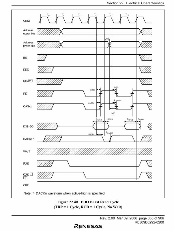
Section 22 Electrical Characteristics
Rev. 2.00 Mar 09, 2006 page 855 of 906REJ09B0292-0200
CKIO
Tp Tr Tc1 Tc2 Tc1 Tc2
tAD
tDACD1
BS
RD/WR
RD
CASxx
RAS
CAS ⋅OE
CKE
D31–D0
DACKn*
WAIT
Addressupper bits
Addresslower bits
tRSD1
tRSD1
tCASD2
tCASD2
tASC
tDACD2
tRDS2
CSn
tRDH6 tRDH6tRDS2
Note: * DACKn waveform when active-high is specified
Figure 22.40 EDO Burst Read Cycle(TRP = 1 Cycle, RCD = 1 Cycle, No Wait)

Section 22 Electrical Characteristics
Rev. 2.00 Mar 09, 2006 page 856 of 906REJ09B0292-0200
CKIO
BS
CSn
RD/WR
RD
CASxx
RAS
CAS ⋅OE
CKE
D31–D0
DACKn
WAIT
Addressupper bits
Addresslower bits
Tp
tCSD1
Trr Trc1 Trc2 Tre
tCASD2 tCASD2 tCASD2
tRASD2 tRASD2 tRASD2
tCSD1
Figure 22.41 DRAM CASCASCASCAS-Before-RASRASRASRAS Refresh Cycle(TRP = 1 Cycle, TRAS = 2 Cycles)
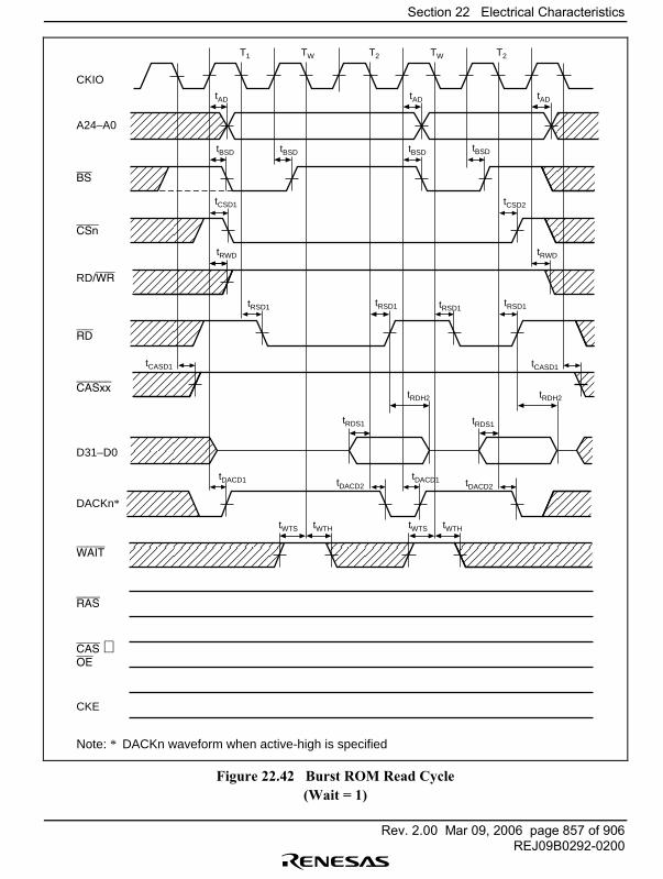
Section 22 Electrical Characteristics
Rev. 2.00 Mar 09, 2006 page 857 of 906REJ09B0292-0200
CKIO
A24–A0
BS
CSn
RD/WR
RD
CASxx
RAS
CAS ⋅OE
CKE
D31–D0
DACKn*
WAIT
T1 TW T2 TW T2
tAD
tBSD
tCSD1
tRWD
tRSD1
tRWD
tBSD tBSD tBSD
tAD tAD
tCSD2
tRSD1
tRDH2
tRDS1
tWTS tWTH tWTS tWTH
tDACD1 tDACD1tDACD2 tDACD2
tRDS1
tRDH2
tCASD1 tCASD1
tRSD1tRSD1
Note: * DACKn waveform when active-high is specified
Figure 22.42 Burst ROM Read Cycle(Wait = 1)
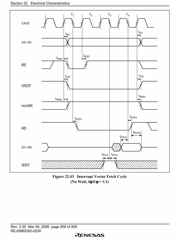
Section 22 Electrical Characteristics
Rev. 2.00 Mar 09, 2006 page 858 of 906REJ09B0292-0200
T1 T2 T3 T4
tADtAD
tRWD
tBSDtBSD
tIVD
tRSD1tRSD1
tRSD1
CKIO
A3–A0
IVECF
RD/WR
RD
D7–D0
BS
tIVD
tRWD
tRDH8
WAIT
tWTS tWTH
Figure 22.43 Interrupt Vector Fetch Cycle(No Wait, Iφφφφ:Eφφφφ = 1:1)
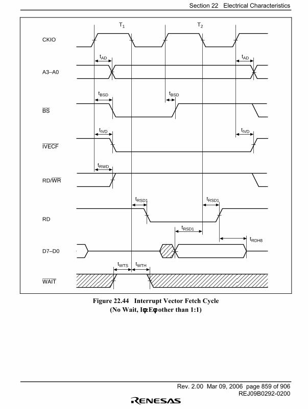
Section 22 Electrical Characteristics
Rev. 2.00 Mar 09, 2006 page 859 of 906REJ09B0292-0200
T1 T2
tAD tAD
tIVD
tRWD
tBSD tBSD
tIVD
tRSD1 tRSD1
tRSD1
CKIO
A3–A0
IVECF
RD/WR
RD
D7–D0
BS
tRDH8
WAIT
tWTS tWTH
Figure 22.44 Interrupt Vector Fetch Cycle(No Wait, Iφφφφ:Eφφφφ other than 1:1)
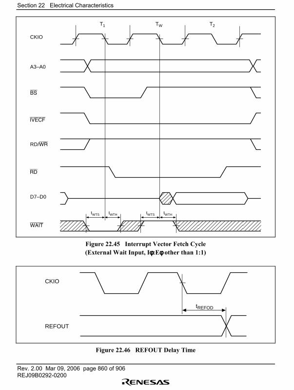
Section 22 Electrical Characteristics
Rev. 2.00 Mar 09, 2006 page 860 of 906REJ09B0292-0200
CKIO
A3–A0
RD/WR
WAIT
D7–D0
RD
IVECF
T1 TW T2
tWTHtWTS tWTHtWTS
BS
Figure 22.45 Interrupt Vector Fetch Cycle(External Wait Input, Iφφφφ:Eφφφφ other than 1:1)
tREFOD
CKIO
REFOUT
Figure 22.46 REFOUT Delay Time
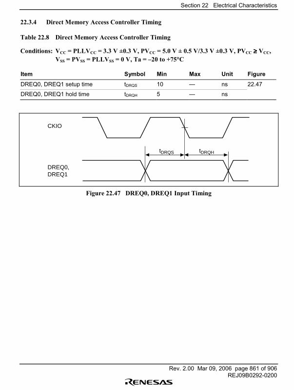
Section 22 Electrical Characteristics
Rev. 2.00 Mar 09, 2006 page 861 of 906REJ09B0292-0200
22.3.4 Direct Memory Access Controller Timing
Table 22.8 Direct Memory Access Controller Timing
Conditions: VCC = PLLVCC = 3.3 V ±0.3 V, PVCC = 5.0 V ± 0.5 V/3.3 V ±0.3 V, PVCC ≥≥≥≥ VCC,VSS = PVSS = PLLVSS = 0 V, Ta = �20 to +75°C
Item Symbol Min Max Unit Figure
DREQ0, DREQ1 setup time tDRQS 10 � ns 22.47
DREQ0, DREQ1 hold time tDRQH 5 � ns
tDRQHtDRQS
CKIO
DREQ0,DREQ1
Figure 22.47 DREQ0, DREQ1 Input Timing
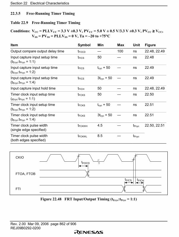
Section 22 Electrical Characteristics
Rev. 2.00 Mar 09, 2006 page 862 of 906REJ09B0292-0200
22.3.5 Free-Running Timer Timing
Table 22.9 Free-Running Timer Timing
Conditions: VCC = PLLVCC = 3.3 V ±0.3 V, PVCC = 5.0 V ± 0.5 V/3.3 V ±0.3 V, PVCC ≥≥≥≥ VCC,VSS = PVSS = PLLVSS = 0 V, Ta = �20 to +75°C
Item Symbol Min Max Unit Figure
Output compare output delay time tFOCD � 100 ns 22.48, 22.49
Input capture input setup time(tEcyc:tPcyc = 1:1)
tFICS 50 � ns 22.48
Input capture input setup time(tEcyc:tPcyc = 1:2)
tFICS tcyc + 50 � ns 22.49
Input capture input setup time(tEcyc:tPcyc = 1:4)
tFICS 3tcyc + 50 � ns 22.49
Input capture input hold time tFICH 50 � ns 22.48, 22.49
Timer clock input setup time(tEcyc:tPcyc = 1:1)
tFCKS 50 � ns 22.50
Timer clock input setup time(tEcyc:tPcyc = 1:2)
tFCKS tcyc + 50 � ns 22.51
Timer clock input setup time(tEcyc:tPcyc = 1:4)
tFCKS 3tcyc + 50 � ns 22.51
Timer clock pulse width(single edge specified)
tFCKWH 4.5 � tPcyc 22.50, 22.51
Timer clock pulse width(both edges specified)
tFCKWL 8.5 � tPcyc
FTOA, FTOB
FTI
CKIO
tFICS tFICH
tFOCD
Figure 22.48 FRT Input/Output Timing (tEcyc:tPcyc = 1:1)
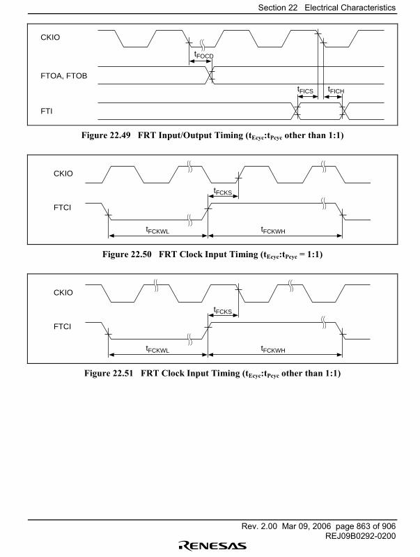
Section 22 Electrical Characteristics
Rev. 2.00 Mar 09, 2006 page 863 of 906REJ09B0292-0200
FTOA, FTOB
FTI
CKIO
tFICS tFICH
tFOCD
Figure 22.49 FRT Input/Output Timing (tEcyc:tPcyc other than 1:1)
CKIO
FTCI
tFCKWL tFCKWH
tFCKS
Figure 22.50 FRT Clock Input Timing (tEcyc:tPcyc = 1:1)
CKIO
FTCI
tFCKWL tFCKWH
tFCKS
Figure 22.51 FRT Clock Input Timing (tEcyc:tPcyc other than 1:1)
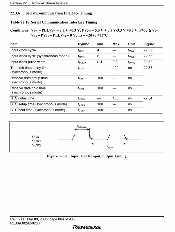
Section 22 Electrical Characteristics
Rev. 2.00 Mar 09, 2006 page 864 of 906REJ09B0292-0200
22.3.6 Serial Communication Interface Timing
Table 22.10 Serial Communication Interface Timing
Conditions: VCC = PLLVCC = 3.3 V ±0.3 V, PVCC = 5.0 V ± 0.5 V/3.3 V ±0.3 V, PVCC ≥≥≥≥ VCC,VSS = PVSS = PLLVSS = 0 V, Ta = �20 to +75°C
Item Symbol Min Max Unit Figure
Input clock cycle tscyc 4 � tPcyc 22.52
Input clock cycle (synchronous mode) tscyc 6 � tPcyc 22.53
Input clock pulse width tSCKW 0.4 0.6 tcscyc 22.52
Transmit data delay time(synchronous mode)
tTXD � 100 ns 22.53
Receive data setup time(synchronous mode)
tRXS 100 � ns
Receive data hold time(synchronous mode)
tRXH 100 � ns
RTS delay time tRTSD � 100 ns 22.54
CTS setup time (synchronous mode) tCTSS 100 � ns
CTS hold time (synchronous mode) tCTSH 100 � ns
tSCKW
tscyc
SCKSCK1SCK2
Figure 22.52 Input Clock Input/Output Timing
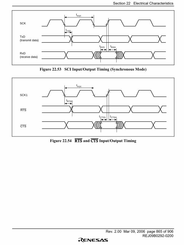
Section 22 Electrical Characteristics
Rev. 2.00 Mar 09, 2006 page 865 of 906REJ09B0292-0200
tscyc
tTXD
tRXS tRXH
SCK
TxD(transmit data)
RxD(receive data)
Figure 22.53 SCI Input/Output Timing (Synchronous Mode)
tscyc
tRTSD
tCTSS tCTSH
SCK1
RTS
CTS
Figure 22.54 RTSRTSRTSRTS and CTSCTSCTSCTS Input/Output Timing
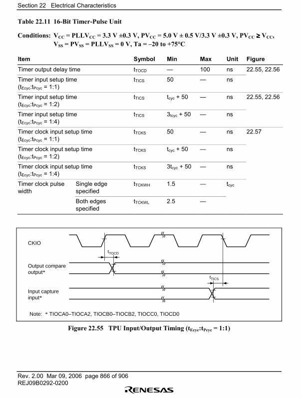
Section 22 Electrical Characteristics
Rev. 2.00 Mar 09, 2006 page 866 of 906REJ09B0292-0200
Table 22.11 16-Bit Timer-Pulse Unit
Conditions: VCC = PLLVCC = 3.3 V ±0.3 V, PVCC = 5.0 V ± 0.5 V/3.3 V ±0.3 V, PVCC ≥≥≥≥ VCC,VSS = PVSS = PLLVSS = 0 V, Ta = �20 to +75°C
Item Symbol Min Max Unit Figure
Timer output delay time tTOCD � 100 ns 22.55, 22.56
Timer input setup time(tEcyc:tPcyc = 1:1)
tTICS 50 � ns
Timer input setup time(tEcyc:tPcyc = 1:2)
tTICS tcyc + 50 � ns 22.55, 22.56
Timer input setup time(tEcyc:tPcyc = 1:4)
tTICS 3tcyc + 50 � ns
Timer clock input setup time(tEcyc:tPcyc = 1:1)
tTCKS 50 � ns 22.57
Timer clock input setup time(tEcyc:tPcyc = 1:2)
tTCKS tcyc + 50 � ns
Timer clock input setup time(tEcyc:tPcyc = 1:4)
tTCKS 3tcyc + 50 � ns
Timer clock pulsewidth
Single edgespecified
tTCKWH 1.5 � tcyc
Both edgesspecified
tTCKWL 2.5 �
tTOCD
tTICS
CKIO
Output compare output*
Input capture input*
Note: * TIOCA0–TIOCA2, TIOCB0–TIOCB2, TIOCC0, TIOCD0
Figure 22.55 TPU Input/Output Timing (tEcyc:tPcyc = 1:1)
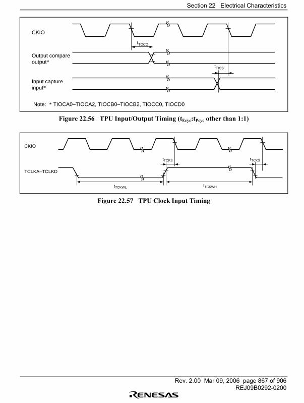
Section 22 Electrical Characteristics
Rev. 2.00 Mar 09, 2006 page 867 of 906REJ09B0292-0200
tTOCD
tTICS
CKIO
Output compare output*
Input capture input*
Note: * TIOCA0–TIOCA2, TIOCB0–TIOCB2, TIOCC0, TIOCD0
Figure 22.56 TPU Input/Output Timing (tEcyc:tPcyc other than 1:1)
tTCKStTCKS
tTCKWL tTCKWH
CKIO
TCLKA–TCLKD
Figure 22.57 TPU Clock Input Timing
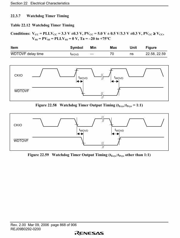
Section 22 Electrical Characteristics
Rev. 2.00 Mar 09, 2006 page 868 of 906REJ09B0292-0200
22.3.7 Watchdog Timer Timing
Table 22.12 Watchdog Timer Timing
Conditions: VCC = PLLVCC = 3.3 V ±0.3 V, PVCC = 5.0 V ± 0.5 V/3.3 V ±0.3 V, PVCC ≥≥≥≥ VCC,VSS = PVSS = PLLVSS = 0 V, Ta = �20 to +75°C
Item Symbol Min Max Unit Figure
WDTOVF delay time tWOVD � 70 ns 22.58, 22.59
CKIO
WDTOVF
tWOVD tWOVD
Figure 22.58 Watchdog Timer Output Timing (tEcyc:tPcyc = 1:1)
CKIO
WDTOVF
tWOVD tWOVD
Figure 22.59 Watchdog Timer Output Timing (tEcyc:tPcyc other than 1:1)
Section 22 Electrical Characteristics
Rev. 2.00 Mar 09, 2006 page 869 of 906REJ09B0292-0200
22.3.8 Serial I/O with FIFO / Serial I/O Timing
Table 22.13 Serial I/O with FIFO / Serial I/O Timing
Conditions: VCC = PLLVCC = 3.3 V ±0.3 V, PVCC = 5.0 V ± 0.5 V/3.3 V ±0.3 V, PVCC ≥≥≥≥ VCC,VSS = PVSS = PLLVSS = 0 V, Ta = �20 to +75°C
Item Symbol Min Max Unit Figure
SRCK0, STCK0 clock input cycle time tSFcyc � 2 tPcyc 22.60
SRCKn, STCKn clock input cycle time(n = 1 or 2)
tSIcyc tPcyc or*66.7
� ns
SRCK0, STCK0 clock input low-level width tSFWL 0.4 × tSFcyc � ns
SRCKn, STCKn clock input low-level width(n = 1 or 2)
tWL 0.4 × tSIcyc � ns
SRCK0, STCK0 clock input high-level width tSFWH 0.4 × tSFcyc � ns
SRCKn, STCKn clock input high-level width(n = 1 or 2)
tWH 0.4 × tSIcyc � ns
SRS input setup time tRSS 15 � ns 22.61
SRS input hold time tRSH 10 � ns
SRXD input setup time tSRDS 15 � ns
SRXD input hold time tSRDH 10 � ns
STS0 input setup time tSFTSS 1 � tPcyc 22.62
STSn input setup time (n = 1 or 2) tTSS 15 � ns
STS input hold time tTSH 10 � ns
STS output delay time tTSD 0 20 ns 22.63
STXD output delay time tTDD 0 20 ns 22.62,22.63
Note: * Specified as tPcyc or 66.7, whichever is greater.

Section 22 Electrical Characteristics
Rev. 2.00 Mar 09, 2006 page 870 of 906REJ09B0292-0200
tSFWH
tSFWL
tSFcyc
STCK0, SRCK0
STCKn, SRCKn
n = 1 or 2
[SIOF]
[SIO]
tWH
tWL
tSIcyc
Figure 22.60 SIOF / SIO Input Clock Timing
SRCKn(input)
SRSn(input)
SRXDn(input)
n = 0, 1, or 2
tSRDS tSRDHtRSS tRSH
Figure 22.61 SIOF / SIO Receive Timing
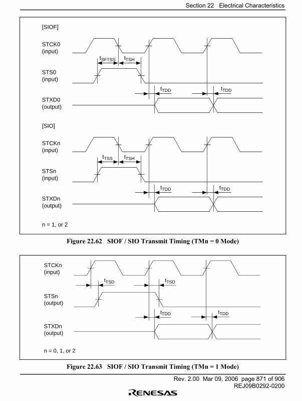
Section 22 Electrical Characteristics
Rev. 2.00 Mar 09, 2006 page 871 of 906REJ09B0292-0200
STCK0(input)
[SIOF]
STS0(input)
STXD0(output)
tTDD tTDD
tSFTSS tTSH
STCKn(input)
[SIO]
STSn(input)
STXDn(output)
n = 1, or 2
tTDD tTDD
tTSS tTSH
Figure 22.62 SIOF / SIO Transmit Timing (TMn = 0 Mode)
STCKn(input)
STSn(output)
STXDn(output)
n = 0, 1, or 2
tTDD tTDD
tTSDtTSD
Figure 22.63 SIOF / SIO Transmit Timing (TMn = 1 Mode)
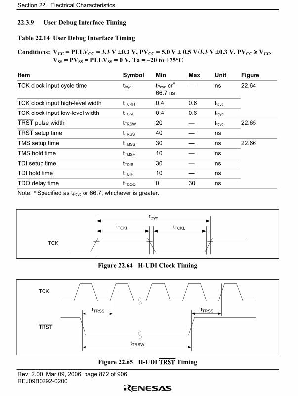
Section 22 Electrical Characteristics
Rev. 2.00 Mar 09, 2006 page 872 of 906REJ09B0292-0200
22.3.9 User Debug Interface Timing
Table 22.14 User Debug Interface Timing
Conditions: VCC = PLLVCC = 3.3 V ±0.3 V, PVCC = 5.0 V ± 0.5 V/3.3 V ±0.3 V, PVCC ≥≥≥≥ VCC,VSS = PVSS = PLLVSS = 0 V, Ta = �20 to +75°C
Item Symbol Min Max Unit Figure
TCK clock input cycle time ttcyc tPcyc or*66.7 ns
� ns 22.64
TCK clock input high-level width tTCKH 0.4 0.6 ttcyc
TCK clock input low-level width tTCKL 0.4 0.6 ttcyc
TRST pulse width tTRSW 20 � ttcyc 22.65
TRST setup time tTRSS 40 � ns
TMS setup time tTMSS 30 � ns 22.66
TMS hold time tTMSH 10 � ns
TDI setup time tTDIS 30 � ns
TDI hold time tTDIH 10 � ns
TDO delay time tTDOD 0 30 nsNote: * Specified as tPcyc or 66.7, whichever is greater.
tTCKH tTCKL
TCK
ttcyc
Figure 22.64 H-UDI Clock Timing
TCK
tTRSS
tTRSW
tTRSS
TRST
Figure 22.65 H-UDI TRSTTRSTTRSTTRST Timing
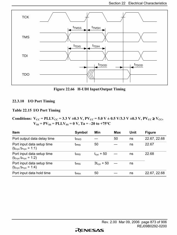
Section 22 Electrical Characteristics
Rev. 2.00 Mar 09, 2006 page 873 of 906REJ09B0292-0200
TCK
TMS
TDI
tTMSS tTMSH
TDO
tTDIS tTDIH
tTDOD tTDOD
Figure 22.66 H-UDI Input/Output Timing
22.3.10 I/O Port Timing
Table 22.15 I/O Port Timing
Conditions: VCC = PLLVCC = 3.3 V ±0.3 V, PVCC = 5.0 V ± 0.5 V/3.3 V ±0.3 V, PVCC ≥≥≥≥ VCC,VSS = PVSS = PLLVSS = 0 V, Ta = �20 to +75°C
Item Symbol Min Max Unit Figure
Port output data delay time tPWD � 50 ns 22.67, 22.68Port input data setup time(tEcyc:tPcyc = 1:1)
tPRS 50 � ns 22.67
Port input data setup time(tEcyc:tPcyc = 1:2)
tPRS tcyc + 50 � ns 22.68
Port input data setup time(tEcyc:tPcyc = 1:4)
tPRS 3tcyc + 50 � ns
Port input data hold time tPRH 50 � ns 22.67, 22.68
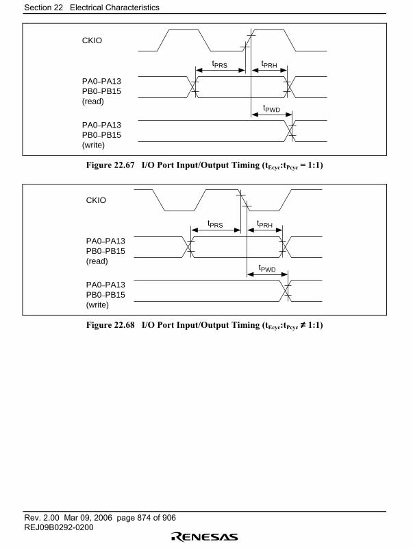
Section 22 Electrical Characteristics
Rev. 2.00 Mar 09, 2006 page 874 of 906REJ09B0292-0200
CKIO
PA0–PA13PB0–PB15(read)
PA0–PA13PB0–PB15(write)
tPWD
tPRS tPRH
Figure 22.67 I/O Port Input/Output Timing (tEcyc:tPcyc = 1:1)
CKIO
PA0–PA13PB0–PB15(read)
PA0–PA13PB0–PB15(write)
tPWD
tPRS tPRH
Figure 22.68 I/O Port Input/Output Timing (tEcyc:tPcyc ≠≠≠≠ 1:1)
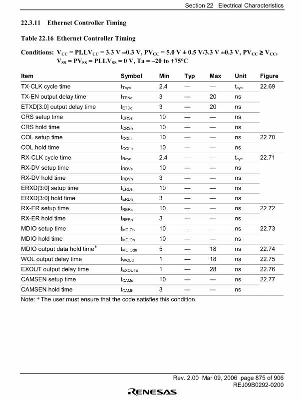
Section 22 Electrical Characteristics
Rev. 2.00 Mar 09, 2006 page 875 of 906REJ09B0292-0200
22.3.11 Ethernet Controller Timing
Table 22.16 Ethernet Controller Timing
Conditions: VCC = PLLVCC = 3.3 V ±0.3 V, PVCC = 5.0 V ± 0.5 V/3.3 V ±0.3 V, PVCC ≥≥≥≥ VCC,VSS = PVSS = PLLVSS = 0 V, Ta = �20 to +75°C
Item Symbol Min Typ Max Unit Figure
TX-CLK cycle time tTcyc 2.4 � � tcyc 22.69
TX-EN output delay time tTENd 3 � 20 ns
ETXD[3:0] output delay time tETDd 3 � 20 ns
CRS setup time tCRSs 10 � � ns
CRS hold time tCRSh 10 � � ns
COL setup time tCOLs 10 � � ns 22.70
COL hold time tCOLh 10 � � ns
RX-CLK cycle time tRcyc 2.4 � � tcyc 22.71
RX-DV setup time tRDVs 10 � � ns
RX-DV hold time tRDVh 3 � � ns
ERXD[3:0] setup time tERDs 10 � � ns
ERXD[3:0] hold time tERDh 3 � � ns
RX-ER setup time tRERs 10 � � ns 22.72
RX-ER hold time tRERh 3 � � ns
MDIO setup time tMDIOs 10 � � ns 22.73
MDIO hold time tMDIOh 10 � � ns
MDIO output data hold time* tMDIOdh 5 � 18 ns 22.74
WOL output delay time tWOLd 1 � 18 ns 22.75
EXOUT output delay time tEXOUTd 1 � 28 ns 22.76
CAMSEN setup time tCAMs 10 � � ns 22.77
CAMSEN hold time tCAMh 3 � � nsNote: * The user must ensure that the code satisfies this condition.
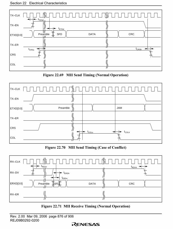
Section 22 Electrical Characteristics
Rev. 2.00 Mar 09, 2006 page 876 of 906REJ09B0292-0200
tTENd
SFD DATA CRC
tCRSh
TX–CLK
TX–EN
ETXD[3:0]
TX–ER
CRS
COL
tCRSs
tETDd
Preamble
Figure 22.69 MII Send Timing (Normal Operation)
Preamble JAM
TX–CLK
TX–EN
ETXD[3:0]
TX–ER
CRS
COL
tCOLhtCOLs
Figure 22.70 MII Send Timing (Case of Conflict)
tRDVs
SFD DATA CRC
RX–CLK
RX–DV
ERXD[3:0]
RX–ER
tERDs
tERDh
tRDVh
Preamble
Figure 22.71 MII Receive Timing (Normal Operation)
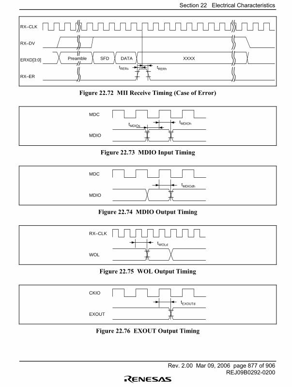
Section 22 Electrical Characteristics
Rev. 2.00 Mar 09, 2006 page 877 of 906REJ09B0292-0200
SFD DATA XXXX
RX– CLK
RX–DV
ERXD[3:0]
RX–ER
tRERs tRERh
Preamble
Figure 22.72 MII Receive Timing (Case of Error)
MDC
tMDIOstMDIOh
MDIO
Figure 22.73 MDIO Input Timing
MDC
tMDIOdh
MDIO
Figure 22.74 MDIO Output Timing
RX–CLK
tWOLd
WOL
Figure 22.75 WOL Output Timing
CKIO
tEXOUTd
EXOUT
Figure 22.76 EXOUT Output Timing

Section 22 Electrical Characteristics
Rev. 2.00 Mar 09, 2006 page 878 of 906REJ09B0292-0200
SFD DATA
RX–CLK
RX–DV
ERXD[3:0]
CAMSEN
tCAMS
Preamble Dest Address Source Address
tCAMh
Figure 22.77 CAMSEN Input Timing
22.3.12 STATS, BHBHBHBH, and BUSHiZBUSHiZBUSHiZBUSHiZ Signal Timing
Table 22.17 STATS, BHBHBHBH, and BUSHiZBUSHiZBUSHiZBUSHiZ Signal Timing
Conditions: VCC = PLLVCC = 3.3 V ±0.3 V, PVCC = 5.0 V ± 0.5 V/3.3 V ±0.3 V, PVCC ≥≥≥≥ VCC,VSS = PVSS = PLLVSS = 0 V, Ta = �20 to +75°C
Item Symbol Min Typ Max Unit Figure
STAS1 and STAS0 output delay time tSTATd � � 16 ns 22.77
BH output rising edge delay time tBHNrd � � 16 ns 22.78
BH output falling edge delay time tBHNfd � � 16 ns
BUSHiZ setup time tBHIZs 7 � � ns 22.79
BUSHiZ hold time tBHIZh 8 � � ns
Output delay time of target pins tBHIZd � � 16 ns
CPU CPU E-DMAC E-DMAC E-DMAC E-DMAC G-DMAC G-DMAC G-DMAC G-DMAC
CKI0
Address
CSn
STATS1, 0
tSTATd
Figure 22.78 STATS Output Timing
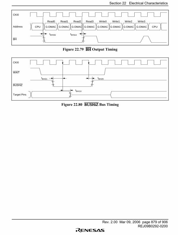
Section 22 Electrical Characteristics
Rev. 2.00 Mar 09, 2006 page 879 of 906REJ09B0292-0200
CPU CPUG-DMAC G-DMAC G-DMAC G-DMAC G-DMACG-DMAC G-DMAC G-DMAC
CKI0
Address
BH
tBHNfd tBHNrd
Read0 Read1 Read2 Read3 Write0 Write1 Write2 Write3
Figure 22.79 BHBHBHBH Output Timing
CKI0
tBHIZs tBHIZh
tBHIZd
WAIT
BUSHiZ
Target Pins
Figure 22.80 BUSHiZBUSHiZBUSHiZBUSHiZ Bus Timing
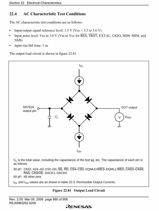
Section 22 Electrical Characteristics
Rev. 2.00 Mar 09, 2006 page 880 of 906REJ09B0292-0200
22.4 AC Characteristic Test Conditions
The AC characteristic test conditions are as follows:
• Input/output signal reference level: 1.5 V (Vcc = 3.3 to 3.6 V)• Input pulse level: Vss to 3.0 V (Vss to Vcc for RES, TRST, EXTAL, CKIO, MD0�MD4, and
NMI)• Input rise/fall time: 1 ns
The output load circuit is shown in figure 22.81.
IOL
CL
SH7616output pin
DUT output
VREF
IOH
CL is the total value, including the capacitance of the test jig, etc. The capacitance of each pin is as follows:
30 pF: CKIO, A24–A0, D31–D0, BS, RD, CS4–CS0, DQMUU/WE3–DQMLL/WE0, CAS3–CAS0, RAS, CAS/OE, DACK1, DACK050 pF: All other pins
IOL and IOH values are as shown in table 22.3, Permissible Output Currents.
V
Figure 22.81 Output Load Circuit
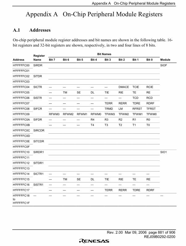
Appendix A On-Chip Peripheral Module Registers
Rev. 2.00 Mar 09, 2006 page 881 of 906REJ09B0292-0200
Appendix A On-Chip Peripheral Module Registers
A.1 Addresses
On-chip peripheral module register addresses and bit names are shown in the following table. 16-bit registers and 32-bit registers are shown, respectively, in two and four lines of 8 bits.
Register Bit Names
Address Name Bit 7 Bit 6 Bit 5 Bit 4 Bit 3 Bit 2 Bit 1 Bit 0 Module
H'FFFFFC00 SIRDR SIOF
H'FFFFFC01
H'FFFFFC02 SITDR
H'FFFFFC03
H'FFFFFC04 SICTR � � � � � DMACE TCIE RCIE
H'FFFFFC05 � TM SE DL TIE RIE TE RE
H'FFFFFC06 SISTR � � � � � � TCD RCD
H'FFFFFC07 � � � � TERR RERR TDRE RDRF
H'FFFFFC08 SIFCR � � � � TRMD LM RFRST TFRST
H'FFFFFC09 RFWM3 RFWM2 RFWM1 RFWM0 TFWM3 TFWM2 TFWM1 TFWM0
H'FFFFFC0A SIFDR � � � R4 R3 R2 R1 R0
H'FFFFFC0B � � � T4 T3 T2 T1 T0
H'FFFFFC0C SIRCDR
H'FFFFFC0D
H'FFFFFC0E SITCDR
H'FFFFFC0F
H'FFFFFC10 SIRDR1 SIO1
H'FFFFFC11
H'FFFFFC12 SITDR1
H'FFFFFC13
H'FFFFFC14 SICTR1 � � � � � � � �
H'FFFFFC15 � TM SE DL TIE RIE TE RE
H'FFFFFC16 SISTR1 � � � � � � � �
H'FFFFFC17 � � � � TERR RERR TDRE RDRF
H'FFFFFC18toH'FFFFFC1F
� � � � � � � � � �
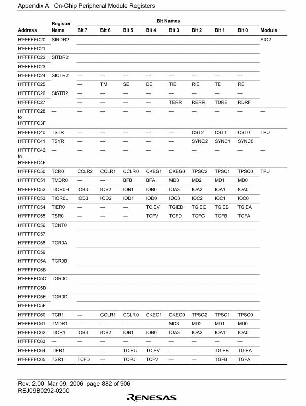
Appendix A On-Chip Peripheral Module Registers
Rev. 2.00 Mar 09, 2006 page 882 of 906REJ09B0292-0200
Register Bit Names
Address Name Bit 7 Bit 6 Bit 5 Bit 4 Bit 3 Bit 2 Bit 1 Bit 0 Module
H'FFFFFC20 SIRDR2 SIO2
H'FFFFFC21
H'FFFFFC22 SITDR2
H'FFFFFC23
H'FFFFFC24 SICTR2 � � � � � � � �
H'FFFFFC25 � TM SE DE TIE RIE TE RE
H'FFFFFC26 SISTR2 � � � � � � � �
H'FFFFFC27 � � � � TERR RERR TDRE RDRF
H'FFFFFC28toH'FFFFFC3F
� � � � � � � � � �
H'FFFFFC40 TSTR � � � � � CST2 CST1 CST0 TPU
H'FFFFFC41 TSYR � � � � � SYNC2 SYNC1 SYNC0
H'FFFFFC42toH'FFFFFC4F
� � � � � � � � � �
H'FFFFFC50 TCR0 CCLR2 CCLR1 CCLR0 CKEG1 CKEG0 TPSC2 TPSC1 TPSC0 TPU
H'FFFFFC51 TMDR0 � � BFB BFA MD3 MD2 MD1 MD0
H'FFFFFC52 TIOR0H IOB3 IOB2 IOB1 IOB0 IOA3 IOA2 IOA1 IOA0
H'FFFFFC53 TIOR0L IOD3 IOD2 IOD1 IOD0 IOC3 IOC2 IOC1 IOC0
H'FFFFFC54 TIER0 � � � TCIEV TGIED TGIEC TGIEB TGIEA
H'FFFFFC55 TSR0 � � � TCFV TGFD TGFC TGFB TGFA
H'FFFFFC56 TCNT0
H'FFFFFC57
H'FFFFFC58 TGR0A
H'FFFFFC59
H'FFFFFC5A TGR0B
H'FFFFFC5B
H'FFFFFC5C TGR0C
H'FFFFFC5D
H'FFFFFC5E TGR0D
H'FFFFFC5F
H'FFFFFC60 TCR1 � CCLR1 CCLR0 CKEG1 CKEG0 TPSC2 TPSC1 TPSC0
H'FFFFFC61 TMDR1 � � � � MD3 MD2 MD1 MD0
H'FFFFFC62 TIOR1 IOB3 IOB2 IOB1 IOB0 IOA3 IOA2 IOA1 IOA0
H'FFFFFC63 � � � � � � � � �
H'FFFFFC64 TIER1 � � TCIEU TCIEV � � TGIEB TGIEA
H'FFFFFC65 TSR1 TCFD � TCFU TCFV � � TGFB TGFA
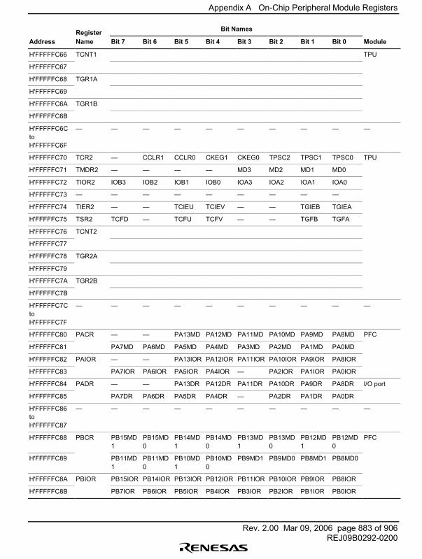
Appendix A On-Chip Peripheral Module Registers
Rev. 2.00 Mar 09, 2006 page 883 of 906REJ09B0292-0200
Register Bit Names
Address Name Bit 7 Bit 6 Bit 5 Bit 4 Bit 3 Bit 2 Bit 1 Bit 0 Module
H'FFFFFC66 TCNT1 TPU
H'FFFFFC67
H'FFFFFC68 TGR1A
H'FFFFFC69
H'FFFFFC6A TGR1B
H'FFFFFC6B
H'FFFFFC6CtoH'FFFFFC6F
� � � � � � � � � �
H'FFFFFC70 TCR2 � CCLR1 CCLR0 CKEG1 CKEG0 TPSC2 TPSC1 TPSC0 TPU
H'FFFFFC71 TMDR2 � � � � MD3 MD2 MD1 MD0
H'FFFFFC72 TIOR2 IOB3 IOB2 IOB1 IOB0 IOA3 IOA2 IOA1 IOA0
H'FFFFFC73 � � � � � � � � �
H'FFFFFC74 TIER2 � � TCIEU TCIEV � � TGIEB TGIEA
H'FFFFFC75 TSR2 TCFD � TCFU TCFV � � TGFB TGFA
H'FFFFFC76 TCNT2
H'FFFFFC77
H'FFFFFC78 TGR2A
H'FFFFFC79
H'FFFFFC7A TGR2B
H'FFFFFC7B
H'FFFFFC7CtoH'FFFFFC7F
� � � � � � � � � �
H'FFFFFC80 PACR � � PA13MD PA12MD PA11MD PA10MD PA9MD PA8MD PFC
H'FFFFFC81 PA7MD PA6MD PA5MD PA4MD PA3MD PA2MD PA1MD PA0MD
H'FFFFFC82 PAIOR � � PA13IOR PA12IOR PA11IOR PA10IOR PA9IOR PA8IOR
H'FFFFFC83 PA7IOR PA6IOR PA5IOR PA4IOR � PA2IOR PA1IOR PA0IOR
H'FFFFFC84 PADR � � PA13DR PA12DR PA11DR PA10DR PA9DR PA8DR I/O port
H'FFFFFC85 PA7DR PA6DR PA5DR PA4DR � PA2DR PA1DR PA0DR
H'FFFFFC86toH'FFFFFC87
� � � � � � � � � �
H'FFFFFC88 PBCR PB15MD1
PB15MD0
PB14MD1
PB14MD0
PB13MD1
PB13MD0
PB12MD1
PB12MD0
PFC
H'FFFFFC89 PB11MD1
PB11MD0
PB10MD1
PB10MD0
PB9MD1 PB9MD0 PB8MD1 PB8MD0
H'FFFFFC8A PBIOR PB15IOR PB14IOR PB13IOR PB12IOR PB11IOR PB10IOR PB9IOR PB8IOR
H'FFFFFC8B PB7IOR PB6IOR PB5IOR PB4IOR PB3IOR PB2IOR PB1IOR PB0IOR
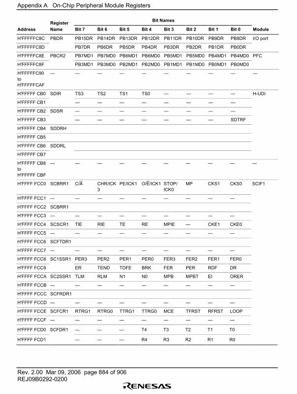
Appendix A On-Chip Peripheral Module Registers
Rev. 2.00 Mar 09, 2006 page 884 of 906REJ09B0292-0200
Register Bit Names
Address Name Bit 7 Bit 6 Bit 5 Bit 4 Bit 3 Bit 2 Bit 1 Bit 0 Module
H'FFFFFC8C PBDR PB15DR PB14DR PB13DR PB12DR PB11DR PB10DR PB9DR PB8DR I/O port
H'FFFFFC8D PB7DR PB6DR PB5DR PB4DR PB3DR PB2DR PB1DR PB0DR
H'FFFFFC8E PBCR2 PB7MD1 PB7MD0 PB6MD1 PB6MD0 PB5MD1 PB5MD0 PB4MD1 PB4MD0 PFC
H'FFFFFC8F PB3MD1 PB3MD0 PB2MD1 PB2MD0 PB1MD1 PB1MD0 PB0MD1 PB0MD0
H'FFFFFC90toH'FFFFFCAF
� � � � � � � � � �
H'FFFFF CB0 SDIR TS3 TS2 TS1 TS0 � � � � H-UDI
H'FFFFF CB1 � � � � � � � �
H'FFFFF CB2 SDSR � � � � � � � �
H'FFFFF CB3 � � � � � � � SDTRF
H'FFFFF CB4 SDDRH
H'FFFFF CB5
H'FFFFF CB6 SDDRL
H'FFFFF CB7
H'FFFFF CB8toH'FFFFF CBF
� � � � � � � � � �
H'FFFF FCC0 SCBRR1 C/A CHR/ICK3
PE/ICK1 O/E/ICK1 STOP/ICK0
MP CKS1 CKS0 SCIF1
H'FFFF FCC1 � � � � � � � � �
H'FFFF FCC2 SCBRR1
H'FFFF FCC3 � � � � � � � � �
H'FFFF FCC4 SCSCR1 TIE RIE TE RE MPIE � CKE1 CKE0
H'FFFF FCC5 � � � � � � � � �
H'FFFF FCC6 SCFTDR1
H'FFFF FCC7 � � � � � � � � �
H'FFFF FCC8 SC1SSR1 PER3 PER2 PER1 PER0 FER3 FER2 FER1 FER0
H'FFFF FCC9 ER TEND TDFE BRK FER PER RDF DR
H'FFFF FCCA SC2SSR1 TLM RLM N1 N0 MPB MPBT EI ORER
H'FFFF FCCB � � � � � � � � �
H'FFFF FCCC SCFRDR1
H'FFFF FCCD � � � � � � � � �
H'FFFF FCCE SCFCR1 RTRG1 RTRG0 TTRG1 TTRG0 MCE TFRST RFRST LOOP
H'FFFF FCCF � � � � � � � � �
H'FFFF FCD0 SCFDR1 � � � T4 T3 T2 T1 T0
H'FFFF FCD1 � � � R4 R3 R2 R1 R0
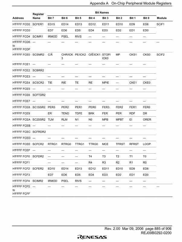
Appendix A On-Chip Peripheral Module Registers
Rev. 2.00 Mar 09, 2006 page 885 of 906REJ09B0292-0200
Register Bit Names
Address Name Bit 7 Bit 6 Bit 5 Bit 4 Bit 3 Bit 2 Bit 1 Bit 0 Module
H'FFFF FCD2 SCFER1 ED15 ED14 ED13 ED12 ED11 ED10 ED9 ED8 SCIF1
H'FFFF FCD3 ED7 ED6 ED5 ED4 ED3 ED2 ED1 ED0
H'FFFF FCD4 SCIMR1 IRMOD PSEL RIVS � � � � �
H'FFFF FCD5toH'FFFF FCDF
� � � � � � � � � �
H'FFFF FCE0 SCSMR2 C/A CHR/ICK3
PE/ICK2 O/E/ICK1 STOP/ICK0
MP CKS1 CKS0 SCIF2
H'FFFF FCE1 � � � � � � � � �
H'FFFF FCE2 SCBRR2
H'FFFF FCE3 � � � � � � � � �
H'FFFF FCE4 SCSCR2 TIE RIE TE RE MPIE � CKE1 CKE0
H'FFFF FCE5 � � � � � � � � �
H'FFFF FCE6 SCFTDR2
H'FFFF FCE7 � � � � � � � � �
H'FFFF FCE8 SC1SSR2 PER3 PER2 PER1 PER0 FER3 FER2 FER1 FER0
H'FFFF FCE9 ER TEND TDFE BRK FER PER RDF DR
H'FFFF FCEA SC2SSR2 TLM RLM N1 N0 MPB MPBT EI ORER
H'FFFF FCEB � � � � � � � � �
H'FFFF FCEC SCFRDR2
H'FFFF FCED � � � � � � � � �
H'FFFF FCEE SCFCR2 RTRG1 RTRG0 TTRG1 TTRG0 MCE TFRST RFRST LOOP
H'FFFF FCEF � � � � � � � � �
H'FFFF FCF0 SCFDR2 � � � T4 T3 T2 T1 T0
H'FFFF FCF1 � � � R4 R3 R2 R1 R0
H'FFFF FCF2 SCFER2 ED15 ED14 ED13 ED12 ED11 ED10 ED9 ED8
H'FFFF FCF3 ED7 ED6 ED5 ED4 ED3 ED2 ED1 ED0
H'FFFF FCF4 SCIMR2 IRMOD PSEL RIVS � � � � �
H'FFFF FCF5toH'FFFF FCFF
� � � � � � � � � �
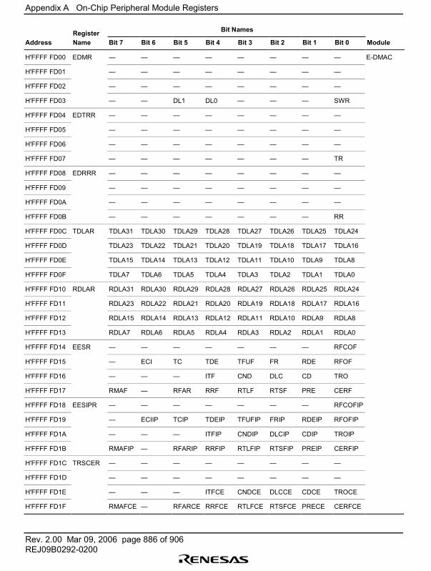
Appendix A On-Chip Peripheral Module Registers
Rev. 2.00 Mar 09, 2006 page 886 of 906REJ09B0292-0200
Register Bit Names
Address Name Bit 7 Bit 6 Bit 5 Bit 4 Bit 3 Bit 2 Bit 1 Bit 0 Module
H'FFFF FD00 EDMR � � � � � � � � E-DMAC
H'FFFF FD01 � � � � � � � �
H'FFFF FD02 � � � � � � � �
H'FFFF FD03 � � DL1 DL0 � � � SWR
H'FFFF FD04 EDTRR � � � � � � � �
H'FFFF FD05 � � � � � � � �
H'FFFF FD06 � � � � � � � �
H'FFFF FD07 � � � � � � � TR
H'FFFF FD08 EDRRR � � � � � � � �
H'FFFF FD09 � � � � � � � �
H'FFFF FD0A � � � � � � � �
H'FFFF FD0B � � � � � � � RR
H'FFFF FD0C TDLAR TDLA31 TDLA30 TDLA29 TDLA28 TDLA27 TDLA26 TDLA25 TDLA24
H'FFFF FD0D TDLA23 TDLA22 TDLA21 TDLA20 TDLA19 TDLA18 TDLA17 TDLA16
H'FFFF FD0E TDLA15 TDLA14 TDLA13 TDLA12 TDLA11 TDLA10 TDLA9 TDLA8
H'FFFF FD0F TDLA7 TDLA6 TDLA5 TDLA4 TDLA3 TDLA2 TDLA1 TDLA0
H'FFFF FD10 RDLAR RDLA31 RDLA30 RDLA29 RDLA28 RDLA27 RDLA26 RDLA25 RDLA24
H'FFFF FD11 RDLA23 RDLA22 RDLA21 RDLA20 RDLA19 RDLA18 RDLA17 RDLA16
H'FFFF FD12 RDLA15 RDLA14 RDLA13 RDLA12 RDLA11 RDLA10 RDLA9 RDLA8
H'FFFF FD13 RDLA7 RDLA6 RDLA5 RDLA4 RDLA3 RDLA2 RDLA1 RDLA0
H'FFFF FD14 EESR � � � � � � � RFCOF
H'FFFF FD15 � ECI TC TDE TFUF FR RDE RFOF
H'FFFF FD16 � � � ITF CND DLC CD TRO
H'FFFF FD17 RMAF � RFAR RRF RTLF RTSF PRE CERF
H'FFFF FD18 EESIPR � � � � � � � RFCOFIP
H'FFFF FD19 � ECIIP TCIP TDEIP TFUFIP FRIP RDEIP RFOFIP
H'FFFF FD1A � � � ITFIP CNDIP DLCIP CDIP TROIP
H'FFFF FD1B RMAFIP � RFARIP RRFIP RTLFIP RTSFIP PREIP CERFIP
H'FFFF FD1C TRSCER � � � � � � � �
H'FFFF FD1D � � � � � � � �
H'FFFF FD1E � � � ITFCE CNDCE DLCCE CDCE TROCE
H'FFFF FD1F RMAFCE � RFARCE RRFCE RTLFCE RTSFCE PRECE CERFCE
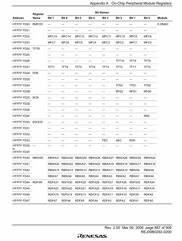
Appendix A On-Chip Peripheral Module Registers
Rev. 2.00 Mar 09, 2006 page 887 of 906REJ09B0292-0200
Register Bit Names
Address Name Bit 7 Bit 6 Bit 5 Bit 4 Bit 3 Bit 2 Bit 1 Bit 0 Module
H'FFFF FD20 RMFCR � � � � � � � � E-DMAC
H'FFFF FD21 � � � � � � � �
H'FFFF FD22 MFC15 MFC14 MFC13 MFC12 MFC11 MFC10 MFC9 MFC8
H'FFFF FD23 MFC7 MFC6 MFC5 MFC4 MFC3 MFC2 MFC1 MFC0
H'FFFF FD24 TFTR � � � � � � � �
H'FFFF FD25 � � � � � � � �
H'FFFF FD26 � � � � � TFT10 TFT9 TFT8
H'FFFF FD27 TFT7 TFT6 TFT5 TFT4 TFT3 TFT2 TFT1 TFT0
H'FFFF FD28 FDR � � � � � � � �
H'FFFF FD29 � � � � � � � �
H'FFFF FD2A � � � � � TFD2 TFD1 TFD0
H'FFFF FD2B � � � � � RFD2 RFD1 RFD0
H'FFFF FD2C RCR � � � � � � � �
H'FFFF FD2D � � � � � � � �
H'FFFF FD2E � � � � � � � �
H'FFFF FD2F � � � � � � � RNC
H'FFFF FD30 EDOCR � � � � � � � �
H'FFFF FD31 � � � � � � � �
H'FFFF FD32 � � � � � � � �
H'FFFF FD33 � � � � FEC AEC EDH �
H'FFFF FD34toH'FFFF FD3F
� � � � � � � � �
H'FFFF FD40 RBWAR RBWA31 RBWA30 RBWA29 RBWA28 RBWA27 RBWA26 RBWA25 RBWA24
H'FFFF FD41 RBWA23 RBWA22 RBWA21 RBWA20 RBWA19 RBWA18 RBWA17 RBWA16
H'FFFF FD42 RBWA15 RBWA14 RBWA13 RBWA12 RBWA11 RBWA10 RBWA9 RBWA8
H'FFFF FD43 RBWA7 RBWA6 RBWA5 RBWA4 RBWA3 RBWA2 RBWA1 RBWA0
H'FFFF FD44 RDFAR RDFA31 RDFA30 RDFA29 RDFA28 RDFA27 RDFA26 RDFA25 RDFA24
H'FFFF FD45 RDFA23 RDFA22 RDFA21 RDFA20 RDFA19 RDFA18 RDFA17 RDFA16
H'FFFF FD46 RDFA15 RDFA14 RDFA13 RDFA12 RDFA11 RDFA10 RDFA9 RDFA8
H'FFFF FD47 RDFA7 RDFA6 RDFA5 RDFA4 RDFA3 RDFA2 RDFA1 RDFA0
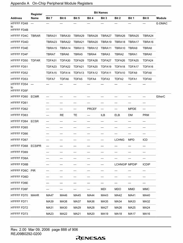
Appendix A On-Chip Peripheral Module Registers
Rev. 2.00 Mar 09, 2006 page 888 of 906REJ09B0292-0200
Register Bit Names
Address Name Bit 7 Bit 6 Bit 5 Bit 4 Bit 3 Bit 2 Bit 1 Bit 0 Module
H'FFFF FD48toH'FFFF FD4B
� � � � � � � � � E-DMAC
H'FFFF FD4C TBRAR TBRA31 TBRA30 TBRA29 TBRA28 TBRA27 TBRA26 TBRA25 TBRA24
H'FFFF FD4D TBRA23 TBRA22 TBRA21 TBRA20 TBRA19 TBRA18 TBRA17 TBRA16
H'FFFF FD4E TBRA15 TBRA14 TBRA13 TBRA12 TBRA11 TBRA10 TBRA9 TBRA8
H'FFFF FD4F TBRA7 TBRA6 TBRA5 TBRA4 TBRA3 TBRA2 TBRA1 TBRA0
H'FFFF FD50 TDFAR TDFA31 TDFA30 TDFA29 TDFA28 TDFA27 TDFA26 TDFA25 TDFA24
H'FFFF FD51 TDFA23 TDFA22 TDFA21 TDFA20 TDFA19 TDFA18 TDFA17 TDFA16
H'FFFF FD52 TDFA15 TDFA14 TDFA13 TDFA12 TDFA11 TDFA10 TDFA9 TDFA8
H'FFFF FD53 TDFA7 TDFA6 TDFA5 TDFA4 TDFA3 TDFA2 TDFA1 TDFA0
H'FFFF FD54toH'FFFF FD5F
� � � � � � � � �
H'FFFF FD60 ECMR � � � � � � � � EtherC
H'FFFF FD61 � � � � � � � �
H'FFFF FD62 � � � PRCEF � � MPDE �
H'FFFF FD63 � RE TE � ILB ELB DM PRM
H'FFFF FD64 ECSR � � � � � � � �
H'FFFF FD65 � � � � � � � �
H'FFFF FD66 � � � � � � � �
H'FFFF FD67 � � � � � LCHNG MPD ICD
H'FFFF FD68 ECSIPR � � � � � � � �
H'FFFF FD69 � � � � � � � �
H'FFFF FD6A � � � � � � � �
H'FFFF FD6B � � � � � LCHNGIP MPDIP ICDIP
H'FFFF FD6C PIR � � � � � � � �
H'FFFF FD6D � � � � � � � �
H'FFFF FD6E � � � � � � � �
H'FFFF FD6F � � � � MDI MDO MMD MMC
H'FFFF FD70 MAHR MA47 MA46 MA45 MA44 MA43 MA42 MA41 MA40
H'FFFF FD71 MA39 MA38 MA37 MA36 MA35 MA34 MA33 MA32
H'FFFF FD72 MA31 MA30 MA29 MA28 MA27 MA26 MA25 MA24
H'FFFF FD73 MA23 MA22 MA21 MA20 MA19 MA18 MA17 MA16

Appendix A On-Chip Peripheral Module Registers
Rev. 2.00 Mar 09, 2006 page 889 of 906REJ09B0292-0200
Register Bit Names
Address Name Bit 7 Bit 6 Bit 5 Bit 4 Bit 3 Bit 2 Bit 1 Bit 0 Module
H'FFFF FD74 MALR � � � � � � � � EtherC
H'FFFF FD75 � � � � � � � �
H'FFFF FD76 MA15 MA14 MA13 MA12 MA11 MA10 MA9 MA8
H'FFFF FD77 MA7 MA6 MA5 MA4 MA3 MA2 MA1 MA0
H'FFFF FD78 RFLR � � � � � � � �
H'FFFF FD79 � � � � � � � �
H'FFFF FD7A � � � � RFL11 RFL10 RFL9 RFL8
H'FFFF FD7B RFL7 RFL6 RFL5 RFL4 RFL3 RFL2 RFL1 RFL0
H'FFFF FD7C PSR � � � � � � � �
H'FFFF FD7D � � � � � � � �
H'FFFF FD7E � � � � � � � �
H'FFFF FD7F � � � � � � � LMON
H'FFFF FD80 TROCR � � � � � � � �
H'FFFF FD81 � � � � � � � �
H'FFFF FD82 TROC15 TROC14 TROC13 TROC12 TROC11 TROC10 TROC9 TROC8
H'FFFF FD83 TROC7 TROC6 TROC5 TROC4 TROC3 TROC2 TROC1 TROC0
H'FFFF FD84 CDCR � � � � � � � �
H'FFFF FD85 � � � � � � � �
H'FFFF FD86 COLDC15 COLDC14 COLDC13 COLDC12 COLDC11 COLDC10 COLDC9 COLDC8
H'FFFF FD87 COLDC7 COLDC6 COLDC5 COLDC4 COLDC3 COLDC2 COLDC1 COLDC0
H'FFFF FD88 LCCR � � � � � � � �
H'FFFF FD89 � � � � � � � �
H'FFFF FD8A LCC15 LCC14 LCC13 LCC12 LCC11 LCC10 LCC9 LCC8
H'FFFF FD8B LCC7 LCC6 LCC5 LCC4 LCC3 LCC2 LCC1 LCC0
H'FFFF FD8C CNDCR � � � � � � � �
H'FFFF FD8D � � � � � � � �
H'FFFF FD8E CNDC15 CNDC14 CNDC13 CNDC12 CNDC11 CNDC10 CNDC9 CNDC8
H'FFFF FD8F CNDC7 CNDC6 CNDC5 CNDC4 CNDC3 CNDC2 CNDC1 CNDC0
H'FFFF FD90 IFLCR � � � � � � � �
H'FFFF FD91 � � � � � � � �
H'FFFF FD92 IFLC15 IFLC14 IFLC13 IFLC12 IFLC11 IFLC10 IFLC9 IFLC8
H'FFFF FD93 IFLC7 IFLC6 IFLC5 IFLC4 IFLC3 IFLC2 IFLC1 IFLC0
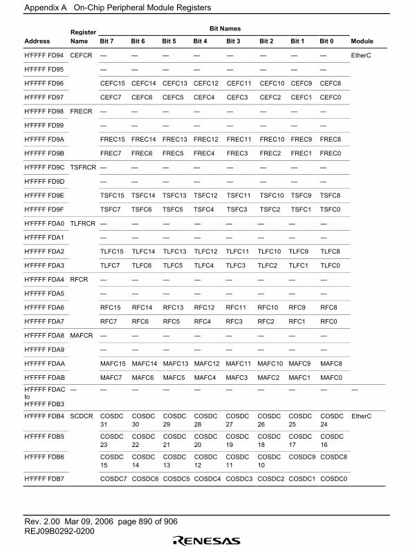
Appendix A On-Chip Peripheral Module Registers
Rev. 2.00 Mar 09, 2006 page 890 of 906REJ09B0292-0200
Register Bit Names
Address Name Bit 7 Bit 6 Bit 5 Bit 4 Bit 3 Bit 2 Bit 1 Bit 0 Module
H'FFFF FD94 CEFCR � � � � � � � � EtherC
H'FFFF FD95 � � � � � � � �
H'FFFF FD96 CEFC15 CEFC14 CEFC13 CEFC12 CEFC11 CEFC10 CEFC9 CEFC8
H'FFFF FD97 CEFC7 CEFC6 CEFC5 CEFC4 CEFC3 CEFC2 CEFC1 CEFC0
H'FFFF FD98 FRECR � � � � � � � �
H'FFFF FD99 � � � � � � � �
H'FFFF FD9A FREC15 FREC14 FREC13 FREC12 FREC11 FREC10 FREC9 FREC8
H'FFFF FD9B FREC7 FREC6 FREC5 FREC4 FREC3 FREC2 FREC1 FREC0
H'FFFF FD9C TSFRCR � � � � � � � �
H'FFFF FD9D � � � � � � � �
H'FFFF FD9E TSFC15 TSFC14 TSFC13 TSFC12 TSFC11 TSFC10 TSFC9 TSFC8
H'FFFF FD9F TSFC7 TSFC6 TSFC5 TSFC4 TSFC3 TSFC2 TSFC1 TSFC0
H'FFFF FDA0 TLFRCR � � � � � � � �
H'FFFF FDA1 � � � � � � � �
H'FFFF FDA2 TLFC15 TLFC14 TLFC13 TLFC12 TLFC11 TLFC10 TLFC9 TLFC8
H'FFFF FDA3 TLFC7 TLFC6 TLFC5 TLFC4 TLFC3 TLFC2 TLFC1 TLFC0
H'FFFF FDA4 RFCR � � � � � � � �
H'FFFF FDA5 � � � � � � � �
H'FFFF FDA6 RFC15 RFC14 RFC13 RFC12 RFC11 RFC10 RFC9 RFC8
H'FFFF FDA7 RFC7 RFC6 RFC5 RFC4 RFC3 RFC2 RFC1 RFC0
H'FFFF FDA8 MAFCR � � � � � � � �
H'FFFF FDA9 � � � � � � � �
H'FFFF FDAA MAFC15 MAFC14 MAFC13 MAFC12 MAFC11 MAFC10 MAFC9 MAFC8
H'FFFF FDAB MAFC7 MAFC6 MAFC5 MAFC4 MAFC3 MAFC2 MAFC1 MAFC0
H'FFFF FDACtoH'FFFF FDB3
� � � � � � � � � �
H'FFFF FDB4 SCDCR COSDC31
COSDC30
COSDC29
COSDC28
COSDC27
COSDC26
COSDC25
COSDC24
EtherC
H'FFFF FDB5 COSDC23
COSDC22
COSDC21
COSDC20
COSDC19
COSDC18
COSDC17
COSDC16
H'FFFF FDB6 COSDC15
COSDC14
COSDC13
COSDC12
COSDC11
COSDC10
COSDC9 COSDC8
H'FFFF FDB7 COSDC7 COSDC6 COSDC5 COSDC4 COSDC3 COSDC2 COSDC1 COSDC0
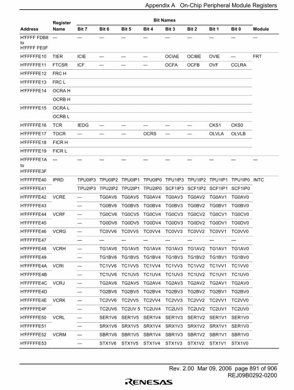
Appendix A On-Chip Peripheral Module Registers
Rev. 2.00 Mar 09, 2006 page 891 of 906REJ09B0292-0200
Register Bit Names
Address Name Bit 7 Bit 6 Bit 5 Bit 4 Bit 3 Bit 2 Bit 1 Bit 0 Module
H'FFFF FDB8toH'FFFF FE0F
� � � � � � � � � �
H'FFFFFE10 TIER ICIE � � � OCIAE OCIBE OVIE � FRT
H'FFFFFE11 FTCSR ICF � � � OCFA OCFB OVF CCLRA
H'FFFFFE12 FRC H
H'FFFFFE13 FRC L
H'FFFFFE14 OCRA H
OCRB H
H'FFFFFE15 OCRA L
OCRB L
H'FFFFFE16 TCR IEDG � � � � � CKS1 CKS0
H'FFFFFE17 TOCR � � � OCRS � � OLVLA OLVLB
H'FFFFFE18 FICR H
H'FFFFFE19 FICR L
H'FFFFFE1AtoH'FFFFFE3F
� � � � � � � � � �
H'FFFFFE40 IPRD TPU0IP3 TPU0IP2 TPU0IP1 TPU0IP0 TPU1IP3 TPU1IP2 TPU1IP1 TPU1IP0 INTC
H'FFFFFE41 TPU2IP3 TPU2IP2 TPU2IP1 TPU2IP0 SCF1IP3 SCF1IP2 SCF1IP1 SCF1IP0
H'FFFFFE42 VCRE � TG0AV6 TG0AV5 TG0AV4 TG0AV3 TG0AV2 TG0AV1 TG0AV0
H'FFFFFE43 � TG0BV6 TG0BV5 TG0BV4 TG0BV3 TG0BV2 TG0BV1 TG0BV0
H'FFFFFE44 VCRF � TG0CV6 TG0CV5 TG0CV4 TG0CV3 TG0CV2 TG0CV1 TG0CV0
H'FFFFFE45 � TG0DV6 TG0DV5 TG0DV4 TG0DV3 TG0DV2 TG0DV1 TG0DV0
H'FFFFFE46 VCRG � TC0VV6 TC0VV5 TC0VV4 TC0VV3 TC0VV2 TC0VV1 TC0VV0
H'FFFFFE47 � � � � � � � �
H'FFFFFE48 VCRH � TG1AV6 TG1AV5 TG1AV4 TG1AV3 TG1AV2 TG1AV1 TG1AV0
H'FFFFFE49 � TG1BV6 TG1BV5 TG1BV4 TG1BV3 TG1BV2 TG1BV1 TG1BV0
H'FFFFFE4A VCRI � TC1VV6 TC1VV5 TC1VV4 TC1VV3 TC1VV2 TC1VV1 TC1VV0
H'FFFFFE4B � TC1UV6 TC1UV5 TC1UV4 TC1UV3 TC1UV2 TC1UV1 TC1UV0
H'FFFFFE4C VCRJ � TG2AV6 TG2AV5 TG2AV4 TG2AV3 TG2AV2 TG2AV1 TG2AV0
H'FFFFFE4D � TG2BV6 TG2BV5 TG2BV4 TG2BV3 TG2BV2 TG2BV1 TG2BV0
H'FFFFFE4E VCRK � TC2VV6 TC2VV5 TC2VV4 TC2VV3 TC2VV2 TC2VV1 TC2VV0
H'FFFFFE4F � TC2UV6 TC2UV 5 TC2UV4 TC2UV3 TC2UV2 TC2UV1 TC2UV0
H'FFFFFE50 VCRL � SER1V6 SER1V5 SER1V4 SER1V3 SER1V2 SER1V1 SER1V0
H'FFFFFE51 � SRX1V6 SRX1V5 SRX1V4 SRX1V3 SRX1V2 SRX1V1 SER1V0
H'FFFFFE52 VCRM � SBR1V6 SBR1V5 SBR1V4 SBR1V3 SBR1V2 SBR1V1 SBR1V0
H'FFFFFE53 � STX1V6 STX1V5 STX1V4 STX1V3 STX1V2 STX1V1 STX1V0
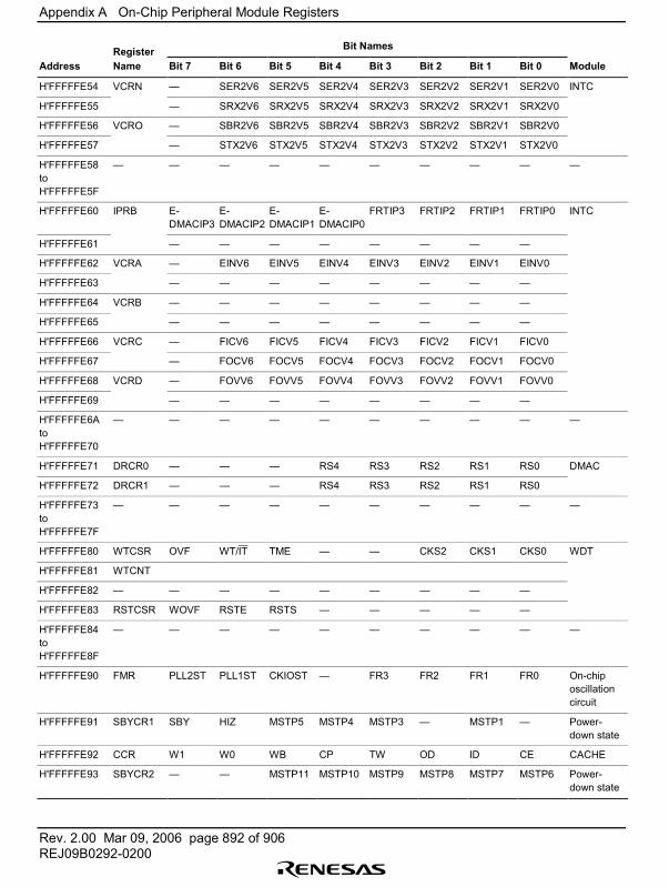
Appendix A On-Chip Peripheral Module Registers
Rev. 2.00 Mar 09, 2006 page 892 of 906REJ09B0292-0200
Register Bit Names
Address Name Bit 7 Bit 6 Bit 5 Bit 4 Bit 3 Bit 2 Bit 1 Bit 0 Module
H'FFFFFE54 VCRN � SER2V6 SER2V5 SER2V4 SER2V3 SER2V2 SER2V1 SER2V0 INTC
H'FFFFFE55 � SRX2V6 SRX2V5 SRX2V4 SRX2V3 SRX2V2 SRX2V1 SRX2V0
H'FFFFFE56 VCRO � SBR2V6 SBR2V5 SBR2V4 SBR2V3 SBR2V2 SBR2V1 SBR2V0
H'FFFFFE57 � STX2V6 STX2V5 STX2V4 STX2V3 STX2V2 STX2V1 STX2V0
H'FFFFFE58toH'FFFFFE5F
� � � � � � � � � �
H'FFFFFE60 IPRB E-DMACIP3
E-DMACIP2
E-DMACIP1
E-DMACIP0
FRTIP3 FRTIP2 FRTIP1 FRTIP0 INTC
H'FFFFFE61 � � � � � � � �
H'FFFFFE62 VCRA � EINV6 EINV5 EINV4 EINV3 EINV2 EINV1 EINV0
H'FFFFFE63 � � � � � � � �
H'FFFFFE64 VCRB � � � � � � � �
H'FFFFFE65 � � � � � � � �
H'FFFFFE66 VCRC � FICV6 FICV5 FICV4 FICV3 FICV2 FICV1 FICV0
H'FFFFFE67 � FOCV6 FOCV5 FOCV4 FOCV3 FOCV2 FOCV1 FOCV0
H'FFFFFE68 VCRD � FOVV6 FOVV5 FOVV4 FOVV3 FOVV2 FOVV1 FOVV0
H'FFFFFE69 � � � � � � � �
H'FFFFFE6AtoH'FFFFFE70
� � � � � � � � � �
H'FFFFFE71 DRCR0 � � � RS4 RS3 RS2 RS1 RS0 DMAC
H'FFFFFE72 DRCR1 � � � RS4 RS3 RS2 RS1 RS0
H'FFFFFE73toH'FFFFFE7F
� � � � � � � � � �
H'FFFFFE80 WTCSR OVF WT/IT TME � � CKS2 CKS1 CKS0 WDT
H'FFFFFE81 WTCNT
H'FFFFFE82 � � � � � � � � �
H'FFFFFE83 RSTCSR WOVF RSTE RSTS � � � � �
H'FFFFFE84toH'FFFFFE8F
� � � � � � � � � �
H'FFFFFE90 FMR PLL2ST PLL1ST CKIOST � FR3 FR2 FR1 FR0 On-chiposcillationcircuit
H'FFFFFE91 SBYCR1 SBY HIZ MSTP5 MSTP4 MSTP3 � MSTP1 � Power-down state
H'FFFFFE92 CCR W1 W0 WB CP TW OD ID CE CACHE
H'FFFFFE93 SBYCR2 � � MSTP11 MSTP10 MSTP9 MSTP8 MSTP7 MSTP6 Power-down state
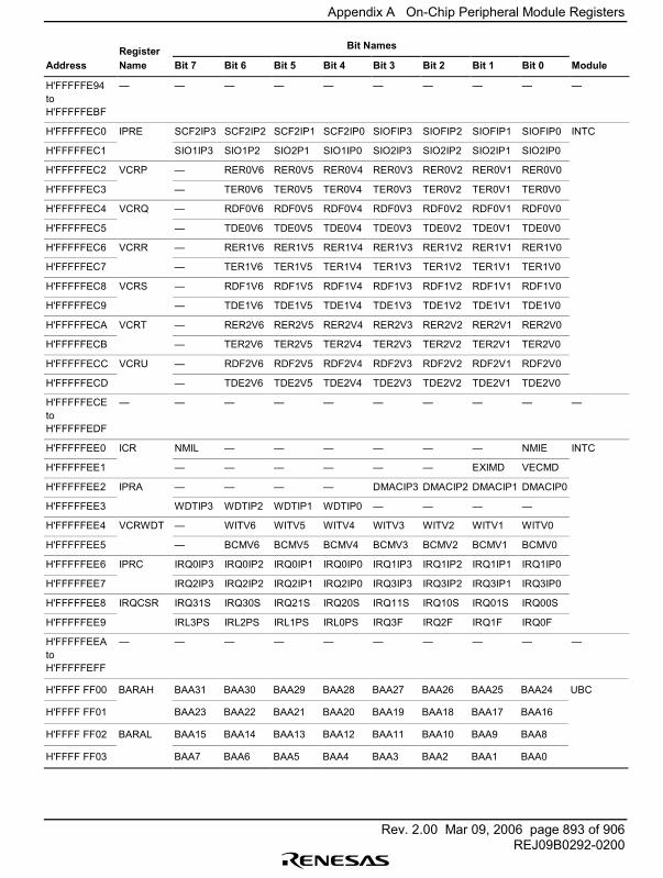
Appendix A On-Chip Peripheral Module Registers
Rev. 2.00 Mar 09, 2006 page 893 of 906REJ09B0292-0200
Register Bit Names
Address Name Bit 7 Bit 6 Bit 5 Bit 4 Bit 3 Bit 2 Bit 1 Bit 0 Module
H'FFFFFE94toH'FFFFFEBF
� � � � � � � � � �
H'FFFFFEC0 IPRE SCF2IP3 SCF2IP2 SCF2IP1 SCF2IP0 SIOFIP3 SIOFIP2 SIOFIP1 SIOFIP0 INTC
H'FFFFFEC1 SIO1IP3 SIO1P2 SIO2P1 SIO1IP0 SIO2IP3 SIO2IP2 SIO2IP1 SIO2IP0
H'FFFFFEC2 VCRP � RER0V6 RER0V5 RER0V4 RER0V3 RER0V2 RER0V1 RER0V0
H'FFFFFEC3 � TER0V6 TER0V5 TER0V4 TER0V3 TER0V2 TER0V1 TER0V0
H'FFFFFEC4 VCRQ � RDF0V6 RDF0V5 RDF0V4 RDF0V3 RDF0V2 RDF0V1 RDF0V0
H'FFFFFEC5 � TDE0V6 TDE0V5 TDE0V4 TDE0V3 TDE0V2 TDE0V1 TDE0V0
H'FFFFFEC6 VCRR � RER1V6 RER1V5 RER1V4 RER1V3 RER1V2 RER1V1 RER1V0
H'FFFFFEC7 � TER1V6 TER1V5 TER1V4 TER1V3 TER1V2 TER1V1 TER1V0
H'FFFFFEC8 VCRS � RDF1V6 RDF1V5 RDF1V4 RDF1V3 RDF1V2 RDF1V1 RDF1V0
H'FFFFFEC9 � TDE1V6 TDE1V5 TDE1V4 TDE1V3 TDE1V2 TDE1V1 TDE1V0
H'FFFFFECA VCRT � RER2V6 RER2V5 RER2V4 RER2V3 RER2V2 RER2V1 RER2V0
H'FFFFFECB � TER2V6 TER2V5 TER2V4 TER2V3 TER2V2 TER2V1 TER2V0
H'FFFFFECC VCRU � RDF2V6 RDF2V5 RDF2V4 RDF2V3 RDF2V2 RDF2V1 RDF2V0
H'FFFFFECD � TDE2V6 TDE2V5 TDE2V4 TDE2V3 TDE2V2 TDE2V1 TDE2V0
H'FFFFFECEtoH'FFFFFEDF
� � � � � � � � � �
H'FFFFFEE0 ICR NMIL � � � � � � NMIE INTC
H'FFFFFEE1 � � � � � � EXIMD VECMD
H'FFFFFEE2 IPRA � � � � DMACIP3 DMACIP2 DMACIP1 DMACIP0
H'FFFFFEE3 WDTIP3 WDTIP2 WDTIP1 WDTIP0 � � � �
H'FFFFFEE4 VCRWDT � WITV6 WITV5 WITV4 WITV3 WITV2 WITV1 WITV0
H'FFFFFEE5 � BCMV6 BCMV5 BCMV4 BCMV3 BCMV2 BCMV1 BCMV0
H'FFFFFEE6 IPRC IRQ0IP3 IRQ0IP2 IRQ0IP1 IRQ0IP0 IRQ1IP3 IRQ1IP2 IRQ1IP1 IRQ1IP0
H'FFFFFEE7 IRQ2IP3 IRQ2IP2 IRQ2IP1 IRQ2IP0 IRQ3IP3 IRQ3IP2 IRQ3IP1 IRQ3IP0
H'FFFFFEE8 IRQCSR IRQ31S IRQ30S IRQ21S IRQ20S IRQ11S IRQ10S IRQ01S IRQ00S
H'FFFFFEE9 IRL3PS IRL2PS IRL1PS IRL0PS IRQ3F IRQ2F IRQ1F IRQ0F
H'FFFFFEEAtoH'FFFFFEFF
� � � � � � � � � �
H'FFFF FF00 BARAH BAA31 BAA30 BAA29 BAA28 BAA27 BAA26 BAA25 BAA24 UBC
H'FFFF FF01 BAA23 BAA22 BAA21 BAA20 BAA19 BAA18 BAA17 BAA16
H'FFFF FF02 BARAL BAA15 BAA14 BAA13 BAA12 BAA11 BAA10 BAA9 BAA8
H'FFFF FF03 BAA7 BAA6 BAA5 BAA4 BAA3 BAA2 BAA1 BAA0
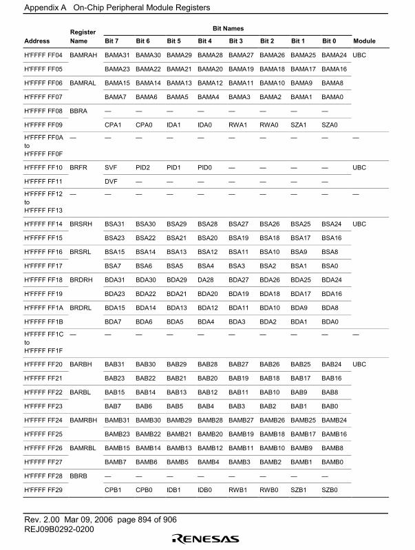
Appendix A On-Chip Peripheral Module Registers
Rev. 2.00 Mar 09, 2006 page 894 of 906REJ09B0292-0200
Register Bit Names
Address Name Bit 7 Bit 6 Bit 5 Bit 4 Bit 3 Bit 2 Bit 1 Bit 0 Module
H'FFFF FF04 BAMRAH BAMA31 BAMA30 BAMA29 BAMA28 BAMA27 BAMA26 BAMA25 BAMA24 UBC
H'FFFF FF05 BAMA23 BAMA22 BAMA21 BAMA20 BAMA19 BAMA18 BAMA17 BAMA16
H'FFFF FF06 BAMRAL BAMA15 BAMA14 BAMA13 BAMA12 BAMA11 BAMA10 BAMA9 BAMA8
H'FFFF FF07 BAMA7 BAMA6 BAMA5 BAMA4 BAMA3 BAMA2 BAMA1 BAMA0
H'FFFF FF08 BBRA � � � � � � � �
H'FFFF FF09 CPA1 CPA0 IDA1 IDA0 RWA1 RWA0 SZA1 SZA0
H'FFFF FF0AtoH'FFFF FF0F
� � � � � � � � � �
H'FFFF FF10 BRFR SVF PID2 PID1 PID0 � � � � UBC
H'FFFF FF11 DVF � � � � � � �
H'FFFF FF12toH'FFFF FF13
� � � � � � � � � �
H'FFFF FF14 BRSRH BSA31 BSA30 BSA29 BSA28 BSA27 BSA26 BSA25 BSA24 UBC
H'FFFF FF15 BSA23 BSA22 BSA21 BSA20 BSA19 BSA18 BSA17 BSA16
H'FFFF FF16 BRSRL BSA15 BSA14 BSA13 BSA12 BSA11 BSA10 BSA9 BSA8
H'FFFF FF17 BSA7 BSA6 BSA5 BSA4 BSA3 BSA2 BSA1 BSA0
H'FFFF FF18 BRDRH BDA31 BDA30 BDA29 DA28 BDA27 BDA26 BDA25 BDA24
H'FFFF FF19 BDA23 BDA22 BDA21 BDA20 BDA19 BDA18 BDA17 BDA16
H'FFFF FF1A BRDRL BDA15 BDA14 BDA13 BDA12 BDA11 BDA10 BDA9 BDA8
H'FFFF FF1B BDA7 BDA6 BDA5 BDA4 BDA3 BDA2 BDA1 BDA0
H'FFFF FF1CtoH'FFFF FF1F
� � � � � � � � � �
H'FFFF FF20 BARBH BAB31 BAB30 BAB29 BAB28 BAB27 BAB26 BAB25 BAB24 UBC
H'FFFF FF21 BAB23 BAB22 BAB21 BAB20 BAB19 BAB18 BAB17 BAB16
H'FFFF FF22 BARBL BAB15 BAB14 BAB13 BAB12 BAB11 BAB10 BAB9 BAB8
H'FFFF FF23 BAB7 BAB6 BAB5 BAB4 BAB3 BAB2 BAB1 BAB0
H'FFFF FF24 BAMRBH BAMB31 BAMB30 BAMB29 BAMB28 BAMB27 BAMB26 BAMB25 BAMB24
H'FFFF FF25 BAMB23 BAMB22 BAMB21 BAMB20 BAMB19 BAMB18 BAMB17 BAMB16
H'FFFF FF26 BAMRBL BAMB15 BAMB14 BAMB13 BAMB12 BAMB11 BAMB10 BAMB9 BAMB8
H'FFFF FF27 BAMB7 BAMB6 BAMB5 BAMB4 BAMB3 BAMB2 BAMB1 BAMB0
H'FFFF FF28 BBRB � � � � � � � �
H'FFFF FF29 CPB1 CPB0 IDB1 IDB0 RWB1 RWB0 SZB1 SZB0
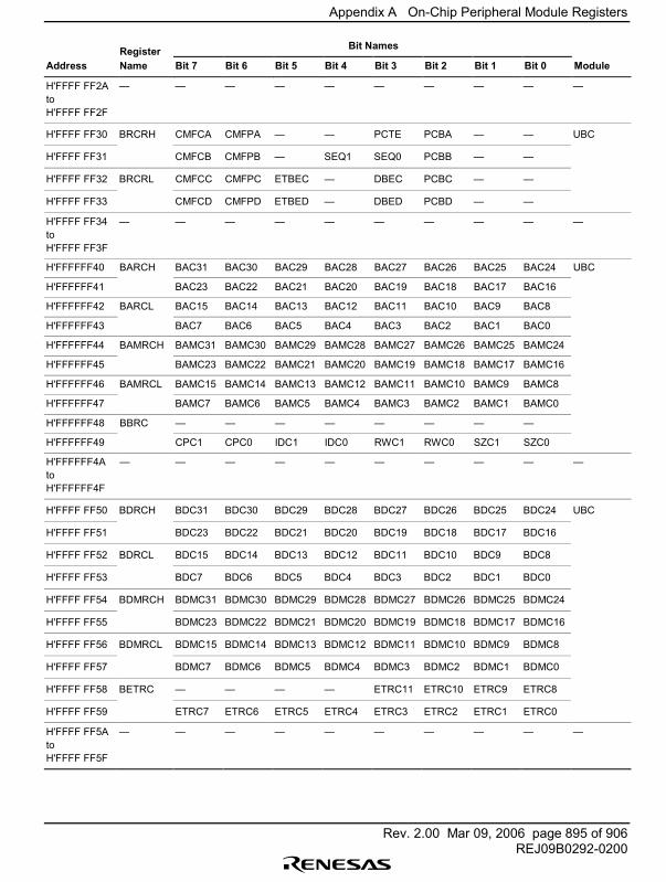
Appendix A On-Chip Peripheral Module Registers
Rev. 2.00 Mar 09, 2006 page 895 of 906REJ09B0292-0200
Register Bit Names
Address Name Bit 7 Bit 6 Bit 5 Bit 4 Bit 3 Bit 2 Bit 1 Bit 0 Module
H'FFFF FF2AtoH'FFFF FF2F
� � � � � � � � � �
H'FFFF FF30 BRCRH CMFCA CMFPA � � PCTE PCBA � � UBC
H'FFFF FF31 CMFCB CMFPB � SEQ1 SEQ0 PCBB � �
H'FFFF FF32 BRCRL CMFCC CMFPC ETBEC � DBEC PCBC � �
H'FFFF FF33 CMFCD CMFPD ETBED � DBED PCBD � �
H'FFFF FF34toH'FFFF FF3F
� � � � � � � � � �
H'FFFFFF40 BARCH BAC31 BAC30 BAC29 BAC28 BAC27 BAC26 BAC25 BAC24 UBC
H'FFFFFF41 BAC23 BAC22 BAC21 BAC20 BAC19 BAC18 BAC17 BAC16
H'FFFFFF42 BARCL BAC15 BAC14 BAC13 BAC12 BAC11 BAC10 BAC9 BAC8
H'FFFFFF43 BAC7 BAC6 BAC5 BAC4 BAC3 BAC2 BAC1 BAC0
H'FFFFFF44 BAMRCH BAMC31 BAMC30 BAMC29 BAMC28 BAMC27 BAMC26 BAMC25 BAMC24
H'FFFFFF45 BAMC23 BAMC22 BAMC21 BAMC20 BAMC19 BAMC18 BAMC17 BAMC16
H'FFFFFF46 BAMRCL BAMC15 BAMC14 BAMC13 BAMC12 BAMC11 BAMC10 BAMC9 BAMC8
H'FFFFFF47 BAMC7 BAMC6 BAMC5 BAMC4 BAMC3 BAMC2 BAMC1 BAMC0
H'FFFFFF48 BBRC � � � � � � � �
H'FFFFFF49 CPC1 CPC0 IDC1 IDC0 RWC1 RWC0 SZC1 SZC0
H'FFFFFF4AtoH'FFFFFF4F
� � � � � � � � � �
H'FFFF FF50 BDRCH BDC31 BDC30 BDC29 BDC28 BDC27 BDC26 BDC25 BDC24 UBC
H'FFFF FF51 BDC23 BDC22 BDC21 BDC20 BDC19 BDC18 BDC17 BDC16
H'FFFF FF52 BDRCL BDC15 BDC14 BDC13 BDC12 BDC11 BDC10 BDC9 BDC8
H'FFFF FF53 BDC7 BDC6 BDC5 BDC4 BDC3 BDC2 BDC1 BDC0
H'FFFF FF54 BDMRCH BDMC31 BDMC30 BDMC29 BDMC28 BDMC27 BDMC26 BDMC25 BDMC24
H'FFFF FF55 BDMC23 BDMC22 BDMC21 BDMC20 BDMC19 BDMC18 BDMC17 BDMC16
H'FFFF FF56 BDMRCL BDMC15 BDMC14 BDMC13 BDMC12 BDMC11 BDMC10 BDMC9 BDMC8
H'FFFF FF57 BDMC7 BDMC6 BDMC5 BDMC4 BDMC3 BDMC2 BDMC1 BDMC0
H'FFFF FF58 BETRC � � � � ETRC11 ETRC10 ETRC9 ETRC8
H'FFFF FF59 ETRC7 ETRC6 ETRC5 ETRC4 ETRC3 ETRC2 ETRC1 ETRC0
H'FFFF FF5AtoH'FFFF FF5F
� � � � � � � � � �
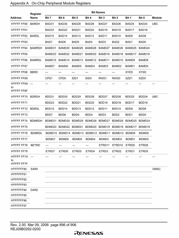
Appendix A On-Chip Peripheral Module Registers
Rev. 2.00 Mar 09, 2006 page 896 of 906REJ09B0292-0200
Register Bit Names
Address Name Bit 7 Bit 6 Bit 5 Bit 4 Bit 3 Bit 2 Bit 1 Bit 0 Module
H'FFFF FF60 BARDH BAD31 BAD30 BAD29 BAD28 BAD27 BAD26 BAD25 BAD24 UBC
H'FFFF FF61 BAD23 BAD22 BAD21 BAD20 BAD19 BAD18 BAD17 BAD16
H'FFFF FF62 BARDL BAD15 BAD14 BAD13 BAD12 BAD11 BAD10 BAD9 BAD8
H'FFFF FF63 BAD7 BAD6 BAD5 BAD4 BAD3 BAD2 BAD1 BAD0
H'FFFF FF64 BAMRDH BAMD31 BAMD30 BAMD29 BAMD28 BAMD27 BAMD26 BAMD25 BAMD24
H'FFFF FF65 BAMD23 BAMD22 BAMD21 BAMD20 BAMD19 BAMD18 BAMD17 BAMD16
H'FFFF FF66 BAMRDL BAMD15 BAMD14 BAMD13 BAMD12 BAMD11 BAMD10 BAMD9 BAMD8
H'FFFF FF67 BAMD7 BAMD6 BAMD5 BAMD4 BAMD3 BAMD2 BAMD1 BAMD0
H'FFFF FF68 BBRD � � � � � � XYED XYSD
H'FFFF FF69 CPD1 CPD0 IDD1 IDD0 RWD1 RWD0 SZD1 SZD0
H'FFFF FF6AtoH'FFFF FF6F
� � � � � � � � � �
H'FFFF FF70 BDRDH BDD31 BDD30 BDD29 BDD28 BDD27 BDD26 BDD25 BDD24 UBC
H'FFFF FF71 BDD23 BDD22 BDD21 BDD20 BDD19 BDD18 BDD17 BDD16
H'FFFF FF72 BDRDL BDD15 BDD14 BDD13 BDD12 BDD11 BDD10 BDD9 BDD8
H'FFFF FF73 BDD7 BDD6 BDD5 BDD4 BDD3 BDD2 BDD1 BDD0
H'FFFF FF74 BDMRDH BDMD31 BDMD30 BDMD29 BDMD28 BDMD27 BDMD26 BDMD25 BDMD24
H'FFFF FF75 BDMD23 BDMD22 BDMD21 BDMD20 BDMD19 BDMD18 BDMD17 BDMD16
H'FFFF FF76 BDMRDL BDMD15 BDMD14 BDMD13 BDMD12 BDMD11 BDMD10 BDMD9 BDMD8
H'FFFF FF77 BDMD7 BDMD6 BDMD5 BDMD4 BDMD3 BDMD2 BDMD1 BDMD0
H'FFFF FF78 BETRD � � � � ETRD11 ETRD10 ETRD9 ETRD8
H'FFFF FF79 ETRD7 ETRD6 ETRD5 ETRD4 ETRD3 ETRD2 ETRD1 ETRD0
H'FFFF FF7AtoH'FFFF FF7F
� � � � � � � � � �
H'FFFFFF80 SAR0 DMAC
H'FFFFFF81
H'FFFFFF82
H'FFFFFF83
H'FFFFFF84 DAR0
H'FFFFFF85
H'FFFFFF86
H'FFFFFF87
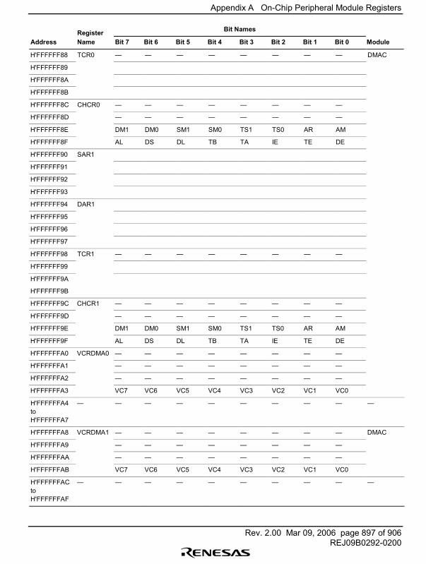
Appendix A On-Chip Peripheral Module Registers
Rev. 2.00 Mar 09, 2006 page 897 of 906REJ09B0292-0200
Register Bit Names
Address Name Bit 7 Bit 6 Bit 5 Bit 4 Bit 3 Bit 2 Bit 1 Bit 0 Module
H'FFFFFF88 TCR0 � � � � � � � � DMAC
H'FFFFFF89
H'FFFFFF8A
H'FFFFFF8B
H'FFFFFF8C CHCR0 � � � � � � � �
H'FFFFFF8D � � � � � � � �
H'FFFFFF8E DM1 DM0 SM1 SM0 TS1 TS0 AR AM
H'FFFFFF8F AL DS DL TB TA IE TE DE
H'FFFFFF90 SAR1
H'FFFFFF91
H'FFFFFF92
H'FFFFFF93
H'FFFFFF94 DAR1
H'FFFFFF95
H'FFFFFF96
H'FFFFFF97
H'FFFFFF98 TCR1 � � � � � � � �
H'FFFFFF99
H'FFFFFF9A
H'FFFFFF9B
H'FFFFFF9C CHCR1 � � � � � � � �
H'FFFFFF9D � � � � � � � �
H'FFFFFF9E DM1 DM0 SM1 SM0 TS1 TS0 AR AM
H'FFFFFF9F AL DS DL TB TA IE TE DE
H'FFFFFFA0 VCRDMA0 � � � � � � � �
H'FFFFFFA1 � � � � � � � �
H'FFFFFFA2 � � � � � � � �
H'FFFFFFA3 VC7 VC6 VC5 VC4 VC3 VC2 VC1 VC0
H'FFFFFFA4toH'FFFFFFA7
� � � � � � � � � �
H'FFFFFFA8 VCRDMA1 � � � � � � � � DMAC
H'FFFFFFA9 � � � � � � � �
H'FFFFFFAA � � � � � � � �
H'FFFFFFAB VC7 VC6 VC5 VC4 VC3 VC2 VC1 VC0
H'FFFFFFACtoH'FFFFFFAF
� � � � � � � � � �
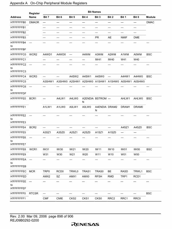
Appendix A On-Chip Peripheral Module Registers
Rev. 2.00 Mar 09, 2006 page 898 of 906REJ09B0292-0200
Register Bit Names
Address Name Bit 7 Bit 6 Bit 5 Bit 4 Bit 3 Bit 2 Bit 1 Bit 0 Module
H'FFFFFFB0 DMAOR � � � � � � � � DMAC
H'FFFFFFB1 � � � � � � � �
H'FFFFFFB2 � � � � � � � �
H'FFFFFFB3 � � � � PR AE NMIF DME
H'FFFFFFB4toH'FFFFFFBF
� � � � � � � � � �
H'FFFFFFC0 WCR2 A4WD1 A4WD0 � A4WM A3WM A2WM A1WM A0WM BSC
H'FFFFFFC1 � � � � IW41 IW40 W41 W40
H'FFFFFFC2toH'FFFFFFC3
� � � � � � � � � �
H'FFFFFFC4 WCR3 � � A4SW2 A4SW1 A4SW0 � A4HW1 A4HW0 BSC
H'FFFFFFC5 A3SHW1 A3SHW0 A2SHW1 A2SHW0 A1SHW1 A1SHW0 A0SHW1 A0SHW0
H'FFFFFFC6toH'FFFFFFDF
� � � � � � � � � �
H'FFFFFFE0 BCR1 � A4LW1 A4LW0 A2ENDIAN
BSTROM � AHLW1 AHLW0 BSC
H'FFFFFFE1 A1LW1 A1LW0 A0LW1 A0LW0 A4ENDIAN
DRAM2 DRAM1 DRAM0
H'FFFFFFE2toH'FFFFFFE3
� � � � � � � � � �
H'FFFFFFE4 BCR2 � � � � � � A4SZ1 A4SZ0 BSC
H'FFFFFFE5 A3SZ1 A3SZ0 A2SZ1 A2SZ0 A1SZ1 A1SZ0 � �
H'FFFFFFE6toH'FFFFFFE7
� � � � � � � � � �
H'FFFFFFE8 WCR1 IW31 IW30 IW21 IW20 IW11 IW10 IW01 IW00 BSC
H'FFFFFFE9 W31 W30 W21 W20 W11 W10 W01 W00
H'FFFFFFEAtoH'FFFFFFEB
� � � � � � � � � �
H'FFFFFFEC MCR TRP0 RCD0 TRWL0 TRAS1 TRAS0 BE RASD TRWL1 BSC
H'FFFFFFED AMX2 SZ AMX1 AMX0 RFSH RMD TRP1 RCD1
H'FFFFFFEEtoH'FFFFFFEF
� � � � � � � � � �
H'FFFFFFF0 RTCSR � � � � � � � � BSC
H'FFFFFFF1 CMF CMIE CKS2 CKS1 CKS0 RRC2 RRC1 RRC0
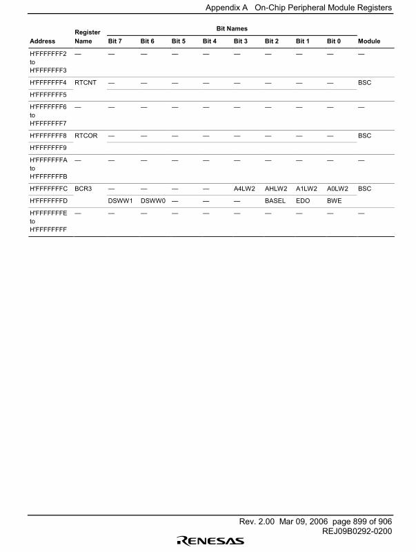
Appendix A On-Chip Peripheral Module Registers
Rev. 2.00 Mar 09, 2006 page 899 of 906REJ09B0292-0200
Register Bit Names
Address Name Bit 7 Bit 6 Bit 5 Bit 4 Bit 3 Bit 2 Bit 1 Bit 0 Module
H'FFFFFFF2toH'FFFFFFF3
� � � � � � � � � �
H'FFFFFFF4 RTCNT � � � � � � � � BSC
H'FFFFFFF5
H'FFFFFFF6toH'FFFFFFF7
� � � � � � � � � �
H'FFFFFFF8 RTCOR � � � � � � � � BSC
H'FFFFFFF9
H'FFFFFFFAtoH'FFFFFFFB
� � � � � � � � � �
H'FFFFFFFC BCR3 � � � � A4LW2 AHLW2 A1LW2 A0LW2 BSC
H'FFFFFFFD DSWW1 DSWW0 � � � BASEL EDO BWE
H'FFFFFFFEtoH'FFFFFFFF
� � � � � � � � � �
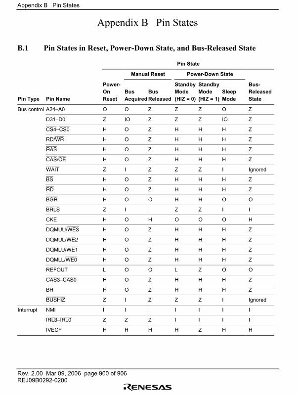
Appendix B Pin States
Rev. 2.00 Mar 09, 2006 page 900 of 906REJ09B0292-0200
Appendix B Pin States
B.1 Pin States in Reset, Power-Down State, and Bus-Released State
Pin State
Manual Reset Power-Down State
Pin Type Pin Name
Power-OnReset
BusAcquired
BusReleased
StandbyMode(HIZ = 0)
StandbyMode(HIZ = 1)
SleepMode
Bus-ReleasedState
Bus control A24�A0 O O Z Z Z O Z
D31�D0 Z IO Z Z Z IO Z
CS4�CS0 H O Z H H H Z
RD/WR H O Z H H H Z
RAS H O Z H H H Z
CAS/OE H O Z H H H Z
WAIT Z I Z Z Z I Ignored
BS H O Z H H H Z
RD H O Z H H H Z
BGR H O O H H O O
BRLS Z I I Z Z I I
CKE H O H O O O H
DQMUU/WE3 H O Z H H H Z
DQMUL/WE2 H O Z H H H Z
DQMLU/WE1 H O Z H H H Z
DQMLL/WE0 H O Z H H H Z
REFOUT L O O L Z O O
CAS3�CAS0 H O Z H H H Z
BH H O Z H H H Z
BUSHiZ Z I Z Z Z I Ignored
Interrupt NMI I I I I I I I
IRL3�IRL0 Z Z Z I I I I
IVECF H H H H Z H H
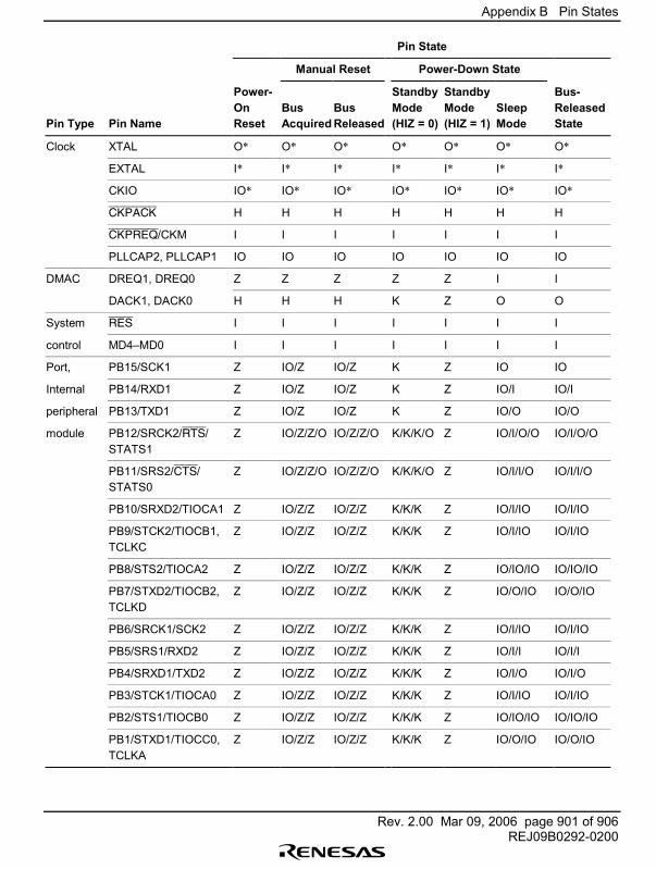
Appendix B Pin States
Rev. 2.00 Mar 09, 2006 page 901 of 906REJ09B0292-0200
Pin State
Manual Reset Power-Down State
Pin Type Pin Name
Power-OnReset
BusAcquired
BusReleased
StandbyMode(HIZ = 0)
StandbyMode(HIZ = 1)
SleepMode
Bus-ReleasedState
Clock XTAL O* O* O* O* O* O* O*
EXTAL I* I* I* I* I* I* I*
CKIO IO* IO* IO* IO* IO* IO* IO*
CKPACK H H H H H H H
CKPREQ/CKM I I I I I I I
PLLCAP2, PLLCAP1 IO IO IO IO IO IO IO
DMAC DREQ1, DREQ0 Z Z Z Z Z I I
DACK1, DACK0 H H H K Z O O
System RES I I I I I I I
control MD4�MD0 I I I I I I I
Port, PB15/SCK1 Z IO/Z IO/Z K Z IO IO
Internal PB14/RXD1 Z IO/Z IO/Z K Z IO/I IO/I
peripheral PB13/TXD1 Z IO/Z IO/Z K Z IO/O IO/O
module PB12/SRCK2/RTS/STATS1
Z IO/Z/Z/O IO/Z/Z/O K/K/K/O Z IO/I/O/O IO/I/O/O
PB11/SRS2/CTS/STATS0
Z IO/Z/Z/O IO/Z/Z/O K/K/K/O Z IO/I/I/O IO/I/I/O
PB10/SRXD2/TIOCA1 Z IO/Z/Z IO/Z/Z K/K/K Z IO/I/IO IO/I/IO
PB9/STCK2/TIOCB1,TCLKC
Z IO/Z/Z IO/Z/Z K/K/K Z IO/I/IO IO/I/IO
PB8/STS2/TIOCA2 Z IO/Z/Z IO/Z/Z K/K/K Z IO/IO/IO IO/IO/IO
PB7/STXD2/TIOCB2,TCLKD
Z IO/Z/Z IO/Z/Z K/K/K Z IO/O/IO IO/O/IO
PB6/SRCK1/SCK2 Z IO/Z/Z IO/Z/Z K/K/K Z IO/I/IO IO/I/IO
PB5/SRS1/RXD2 Z IO/Z/Z IO/Z/Z K/K/K Z IO/I/I IO/I/I
PB4/SRXD1/TXD2 Z IO/Z/Z IO/Z/Z K/K/K Z IO/I/O IO/I/O
PB3/STCK1/TIOCA0 Z IO/Z/Z IO/Z/Z K/K/K Z IO/I/IO IO/I/IO
PB2/STS1/TIOCB0 Z IO/Z/Z IO/Z/Z K/K/K Z IO/IO/IO IO/IO/IO
PB1/STXD1/TIOCC0,TCLKA
Z IO/Z/Z IO/Z/Z K/K/K Z IO/O/IO IO/O/IO
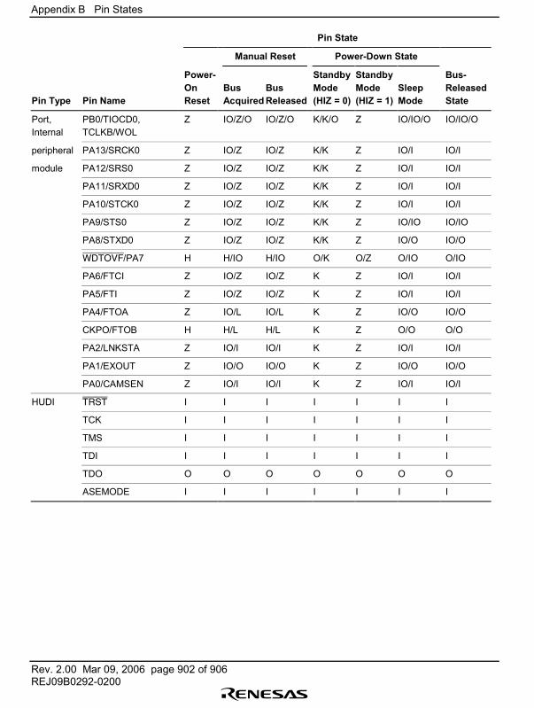
Appendix B Pin States
Rev. 2.00 Mar 09, 2006 page 902 of 906REJ09B0292-0200
Pin State
Manual Reset Power-Down State
Pin Type Pin Name
Power-OnReset
BusAcquired
BusReleased
StandbyMode(HIZ = 0)
StandbyMode(HIZ = 1)
SleepMode
Bus-ReleasedState
Port,Internal
PB0/TIOCD0,TCLKB/WOL
Z IO/Z/O IO/Z/O K/K/O Z IO/IO/O IO/IO/O
peripheral PA13/SRCK0 Z IO/Z IO/Z K/K Z IO/I IO/I
module PA12/SRS0 Z IO/Z IO/Z K/K Z IO/I IO/I
PA11/SRXD0 Z IO/Z IO/Z K/K Z IO/I IO/I
PA10/STCK0 Z IO/Z IO/Z K/K Z IO/I IO/I
PA9/STS0 Z IO/Z IO/Z K/K Z IO/IO IO/IO
PA8/STXD0 Z IO/Z IO/Z K/K Z IO/O IO/O
WDTOVF/PA7 H H/IO H/IO O/K O/Z O/IO O/IO
PA6/FTCI Z IO/Z IO/Z K Z IO/I IO/I
PA5/FTI Z IO/Z IO/Z K Z IO/I IO/I
PA4/FTOA Z IO/L IO/L K Z IO/O IO/O
CKPO/FTOB H H/L H/L K Z O/O O/O
PA2/LNKSTA Z IO/I IO/I K Z IO/I IO/I
PA1/EXOUT Z IO/O IO/O K Z IO/O IO/O
PA0/CAMSEN Z IO/I IO/I K Z IO/I IO/I
HUDI TRST I I I I I I I
TCK I I I I I I I
TMS I I I I I I I
TDI I I I I I I I
TDO O O O O O O O
ASEMODE I I I I I I I
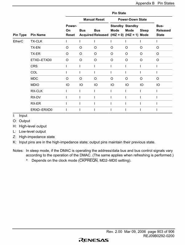
Appendix B Pin States
Rev. 2.00 Mar 09, 2006 page 903 of 906REJ09B0292-0200
Pin State
Manual Reset Power-Down State
Pin Type Pin Name
Power-OnReset
BusAcquired
BusReleased
StandbyMode(HIZ = 0)
StandbyMode(HIZ = 1)
SleepMode
Bus-ReleasedState
EtherC TX-CLK I I I I I I I
TX-EN O O O O O O O
TX-ER O O O O O O O
ETXD�ETXD0 O O O O O O O
CRS I I I I I I I
COL I I I I I I I
MDC O O O O O O O
MDIO IO IO IO IO IO IO IO
RX-CLK I I I I I I I
RX-DV I I I I I I I
RX-ER I I I I I I I
ERXD�ERXD0 I I I I I I I
I: InputO: OutputH: High-level outputL: Low-level outputZ: High-impedance stateK: Input pins are in the high-impedance state; output pins maintain their previous state.
Notes: In sleep mode, if the DMAC is operating the address/data bus and bus control signals varyaccording to the operation of the DMAC. (The same applies when refreshing is performed.)* Depends on the clock mode (CKPREQN, MD2�MD0 setting).
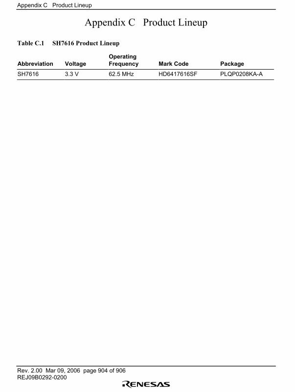
Appendix C Product Lineup
Rev. 2.00 Mar 09, 2006 page 904 of 906REJ09B0292-0200
Appendix C Product Lineup
Table C.1 SH7616 Product Lineup
Abbreviation VoltageOperatingFrequency Mark Code Package
SH7616 3.3 V 62.5 MHz HD6417616SF PLQP0208KA-A
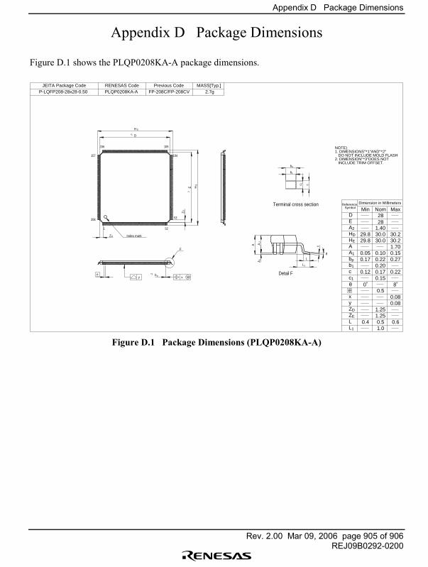
Appendix D Package Dimensions
Rev. 2.00 Mar 09, 2006 page 905 of 906REJ09B0292-0200
Appendix D Package Dimensions
Figure D.1 shows the PLQP0208KA-A package dimensions.
NOTE)1. DIMENSIONS"*1"AND"*2"
DO NOT INCLUDE MOLD FLASH2. DIMENSION"*3"DOES NOT
INCLUDE TRIM OFFSET.
Index mark
*1
2
*3p
E
D
E
D
x My
F
1
208 53
52
157
156
104
105
Z
Z
D
H
E H
b
21
1
Detail F
c
LA
A
A
L
Terminal cross section
p
1
1 c
b
b
c
1.251.25
0.080.08
0.58˚0˚
29.8 30.0 30.2
0.15
0.20
1.700.150.100.050.270.220.17
0.220.170.12
D
L1
ZE
ZD
yx
cb1
bp
A
HD
A2
E
A1
c1
e
e
L
HE
0.60.50.4
MaxNomMinDimension in Millimeters
SymbolReference
281.40
30.230.029.8
1.0
28
θ
θ
P-LQFP208-28x28-0.50 2.7gMASS[Typ.]
FP-208C/FP-208CVPLQP0208KA-ARENESAS CodeJEITA Package Code Previous Code
Figure D.1 Package Dimensions (PLQP0208KA-A)
Appendix D Package Dimensions
Rev. 2.00 Mar 09, 2006 page 906 of 906REJ09B0292-0200
Renesas 32-Bit RISC MicrocomputerHardware ManualSH7616Publication Date: 1st Edition, November 2001
Rev.2.00, March 09, 2006Published by: Sales Strategic Planning Div.
Renesas Technology Corp.Edited by: Customer Support Department
Global Strategic Communication Div.Renesas Solutions Corp.
©2006. Renesas Technology Corp., All rights reserved. Printed in Japan.
Sales Strategic Planning Div. Nippon Bldg., 2-6-2, Ohte-machi, Chiyoda-ku, Tokyo 100-0004, Japan
http://www.renesas.comRefer to "http://www.renesas.com/en/network" for the latest and detailed information.
Renesas Technology America, Inc.450 Holger Way, San Jose, CA 95134-1368, U.S.ATel: <1> (408) 382-7500, Fax: <1> (408) 382-7501 Renesas Technology Europe LimitedDukes Meadow, Millboard Road, Bourne End, Buckinghamshire, SL8 5FH, U.K.Tel: <44> (1628) 585-100, Fax: <44> (1628) 585-900
Renesas Technology (Shanghai) Co., Ltd.Unit 204, 205, AZIACenter, No.1233 Lujiazui Ring Rd, Pudong District, Shanghai, China 200120Tel: <86> (21) 5877-1818, Fax: <86> (21) 6887-7898 Renesas Technology Hong Kong Ltd.7th Floor, North Tower, World Finance Centre, Harbour City, 1 Canton Road, Tsimshatsui, Kowloon, Hong Kong Tel: <852> 2265-6688, Fax: <852> 2730-6071
Renesas Technology Taiwan Co., Ltd.10th Floor, No.99, Fushing North Road, Taipei, TaiwanTel: <886> (2) 2715-2888, Fax: <886> (2) 2713-2999 Renesas Technology Singapore Pte. Ltd.1 Harbour Front Avenue, #06-10, Keppel Bay Tower, Singapore 098632 Tel: <65> 6213-0200, Fax: <65> 6278-8001
Renesas Technology Korea Co., Ltd.Kukje Center Bldg. 18th Fl., 191, 2-ka, Hangang-ro, Yongsan-ku, Seoul 140-702, KoreaTel: <82> (2) 796-3115, Fax: <82> (2) 796-2145 Renesas Technology Malaysia Sdn. BhdUnit 906, Block B, Menara Amcorp, Amcorp Trade Centre, No.18, Jalan Persiaran Barat, 46050 Petaling Jaya, Selangor Darul Ehsan, MalaysiaTel: <603> 7955-9390, Fax: <603> 7955-9510
RENESAS SALES OFFICES
Colophon 6.0

SH7616Hardware Manual