Embed Size (px)
Citation preview
SEM/FIB STAGE CALIBRATION WITH PHOTOGRAMMETRIC METHODS
M. Ritter a, M. Hemmleb b, P. Faber c, B. Lich c, H. Hohenberg d
a Federal Institute for Materials Research and Testing (BAM), 12200 Berlin, Germany - ([email protected]) b Matthias Hemmleb, 14482 Potsdam - ([email protected])
c FEI Company, PO Box 80066, 5600 KA Eindhoven, The Netherlands - (blich, [email protected]) d Heinrich-Pette-Institute for Experimental Virology and Immunology at the University of Hamburg, Martinistrasse 52,
20251 Hamburg, Germany - ([email protected])
Commission V, WG 1
Key Words: Metrology, Microscopy, Calibration, Bundle, Adjustment, Accuracy Abstract: Precise sample stage positioning plays an important role for various FIB (Focused Ion Beam) and SEM (scanning electron microscope) applications in micro- and nanotechnology. During the last few years, FIB instruments have become an indispensable tool for sample preparation, prototyping and micro-machining. Modern FIB devices are equipped with an additional electron column. Such combined SEM/FIB devices not only offer the possibility of forming structures by the focused ion beam, but also to almost instantly image the results in a non-destructive manner with the electron probe. Because of the fact that the ion column and the electron column are located at different positions in respect to each another, the sample has to be orientated normal to the beam by a positioning stage. Within a joint project we investigated the accuracy of SEM/FIB positioning stage operations. Therefore, the repetition uncertainty of the positioning stage was determined by applying photogrammetric methods that were adapted to the micro-range for the geometrical calibration of SEMs, and, by using a special 3D calibration structure with control points of approximately 100 nm in diameter (nanomarker). Photogrammetric calibration and analysis of the SEM/FIB system using the nanomarker coordinates worked reliably. The tilting repetition uncertainty of the positioning stage determined by photogrammetric self-calibration was less than 0.03 degrees, whereas the rotation repetition uncertainty was less than 0.09 degrees. With the resulting measurement uncertainties, metrological analysis of prototyping and micro-machining processes is possible in future.
1. INTRODUCTION The FIB technique has been applied in a variety of scientific and technological fields, as well as in industrial tasks, e.g., failure analysis, design modification and process control, because of its ability to create deliberate structures or sample modifications at the micrometer range and below. First and foremost, the semiconductor industry uses FIB devices for integrated circuit (IC) control and modification, and sometimes for mask repair (Giannuzzi, 2005). Other frequently carried out industrial applications using FIB instruments are thin film head manufacturing and lithography. In life science and materials research, the FIB is used to prepare desired planes of interest, usually cross-sections (Bravman, 1984; Stevie, 1995) that are thin enough to be analyzed by transmission electron microscopy (TEM). Combined SEM/FIB devices (fig. 1) not only allow the formation of cross-sections with all kinds of samples by using the ion beam, but also direct imaging with SEM resolution, or, analytical applications using the electron probe. Additionally, multiple cross-sections (slices) can be produced (FIB serial sectioning), each slice subsequently imaged in SEM mode, and, all slices 3D reconstructed by serial tomography algorithms (Sakamoto, 1998). For the purpose of alternating between FIB, SEM and analytic modes, the sample has to be precisely moved, rotated and tilted by a positioning stage in order to align the sections to the respective beam or detector (figs. 1 and 2). In a cooperation project of FEI Company (Eindhoven, the Netherlands) and the Heinrich-Pette-Institute (Hamburg, Germany), we analyzed the positioning accuracy of a special high-precision sample stage of a FEI SEM/FIB (DualBeam) prototype by photogrammetric means.
Photogrammetric methods can be applied for the quantitative 3D surface reconstruction of SEM data, or, the calibration of the imaging properties of SEM (Hemmleb, 2001). When using a suitable (preferably spatial) reference structure, the photogrammetric calibration also delivers the orientation data of the SEM calibration images. Because in the SEM, the sample and not the sensor is moved in order to get images from different perspectives, the orientation data obtained by photogrammetric analysis are equivalent to the sample stage orientation in microscopes (Sinram, 2002). Note the fact that here, the SEM/FIB stage is calibrated by a reference structure created by the very same SEM/FIB device, which is a proof for its combined micro-fabrication and analysis capabilities.
2. SEM/FIB TECHNOLOGY AND THE IMPORTANCE OF STAGE CALIBRATION
The Focused Ion Beam (FIB) works similarly to a scanning electron microscope (SEM), but its capabilities go far beyond imaging (Orloff, 2003). The fundamental difference between FIB and SEM is the use of an ion beam instead of an electron beam. Because ions are much larger and heavier than electrons, other characteristics of sample interaction and imaging apply. In particular, the high momentum of the ions is transferred to the sample atoms within a short distance. The resulting speed and energy of the sample atoms are eventually high enough to remove them from the surrounding matrix. This process is called milling and can be deliberately applied for the fabrication of micro- and nanostructures. Alternatively, in the controlled presence of a special - e.g., organometallic - gas within the specimen chamber, the ions of the beam interact with the gas
adsorbed on the sample surface. The gas is decomposed by the interaction with the ion beam into a volatile organic component, and a solid metallic component that attaches to the substrate surface. Continuous decomposition and attachment can be used for a deliberate build-up of metal layers. This process is called deposition, or, more accurately chemical vapour deposition (CVD) and requires a special gas-insertion system (GIS) (fig. 1). Both micro- and nanofabrication processes are referred to as patterning and are used for a growing number of applications, like the production of micrometer-sized geometrical structures (figs. 2 and 3).
Figure 1. Basic components of SEM/FIB systems: vacuum chamber, ion optical column, electron optical column, tilt stage and
gas-insertion system (GIS)
The FIB instrument consists of a vacuum system, a source, an optical column, the stage and one, or, eventually more detectors (fig. 1). FIB instruments are available as stand-alone single beam devices. However, most recent systems incorporate an additional electron beam column and therefore are called DualBeam (FEI Company), or, CrossBeam (LEO Electron Microscopy GmbH) systems. For the experiments described here, a DualBeam (with a Nova Nanolab 600 stage) operated at the FEI application laboratories (Eindhoven, the Netherlands) could be used.
Figure 2. SEM image of microstructure array fabricated by FIB induced platinum deposition.
Left: Stage positioned normal to electron beam (0 deg.) Right: Stage positioned normal to ion beam (52 deg.)
At this SEM/FIB device, the electron optical column is mounted vertically, whereas the ion column is attached to the specimen chamber at an angle of 52 degrees with respect to the electron column (figs. 1 and 2). As already mentioned, a big advantage of these SEM/FIB systems is the combination of micro-
fabrication by the FIB with the possibility of in-situ analysis and non-destructive imaging in the SEM mode. In this case, the sample stage has to move between patterning (FIB), imaging (SEM) or analysis positions. These movements can include primary tilting of the stage of up to 70 degrees, as well as rotations of up to 90 degrees and additional translations. Therefore, the accuracy of the patterning or analysis processes depends on the accuracy of the used positioning device. With the photogrammetric investigation of the stage accuracy and its calibration, the direct metrological analysis of FIB patterning processes and analytical investigations is possible.
3. APPLICATION OF PHOTOGRAMMETRIC METHODS IN MICRO- AND NANOSCALE
The SEM has been an excellent candidate for photogrammetric analysis from early on (Oshima, 1970; Boyde, 1970), because it provides high resolution, a large depth of field, and images can be captured over a wide range of magnification, very much in contrast to optical microscopes. Additionally, the good signal to noise ratio makes the combination of SEM imaging and photogrammetric analysis very interesting for 3D evaluation in the fields of materials science, quality control and life science. Because SEM images are now almost exclusively generated and stored as digital data, the photogrammetric method is also a good basis for the automation of 3D reconstruction of SEM data (Koenig, 1987). However, not only has the area-based generation of topographic maps been put in the foreground of SEM 3D imaging, but also point measurements (Hemmleb, 1995), and the calibration of the microscopes by photogrammetric means for high precision length and angle measurements (Maune, 1975). 2.1 Image Geometry and Calibration Methods The SEM magnetic or electrostatic lenses produce a virtual projection centre at a large focal length with the coordinates z0 that equal the central point in the central projection case. However, z0 is completely dependent on the working distance wd that is adjusted by the user, whereas the distance from the virtual projection centre to the aperture diaphragm kz is constant and can be calculated according to (Reimer, 1998). The correct determination of this principle distance has a large effect on the calculation of the height of an imaged object (Howell, 1978) in the case of central projection at low magnifications. At magnifications higher than 500x, (Boyde 73) has shown that the parallel projection geometries should be assumed. When parallel projection geometry is used as the functional model, the parameters of the collinearity equations are reduced by z0, because parallel rays do not intersect in one central point. The missing projection centre has a broad effect on the geometrical model. First, it is not possible to construct a perpendicular to the image plane, known as the principal point. Second, there is no distinct focal length, i.e. the distance from the principal point to the projection centre. Therefore, instead of the image constant ck the magnification factor m has to be used (El Ghazali, 1984). However, the magnification and orientation parameters of the image planes are only approximately known in SEM images, therefore a calibration process of the system is required. For scanning electron microscopes used as a 2D measuring instrument, the calibration procedure has to take into account parameters of the scanning optical system (such as the magnification m) as well as additional distortions caused by the imaging process for any adjusted settings of the device. The 3D
calibration of an SEM instrument additionally implies the determination of the exterior orientation parameters for any chosen electron optical settings. A change in settings may be a change in acceleration voltage, switching the spot size or altering the working distance for imaging. In general it implies an alteration to the scanning parameters of the SEM, and hence a probable change in the interior orientation parameters. In order to mathematically take into account a magnification factor for each scanning direction and the distortions for the calibration of any SEM, the functional model of parallel projection is expanded by non-linear correction terms (Maune, 1975). For the calibration process, the least-squares estimation on the basis of the collinearity equations (without or with non-linear distortions) is used. Because this approach describes the best possible fit of corresponding (homologous) image rays to their object coordinates, it is called bundle block adjustment, although with parallel imaging geometry. If only image coordinates are used within the least-squares estimation using a bundle block adjustment for the determination of the desired unknown parameters, it can be called a self-calibration. Because there are no natural control points available on SEM samples, the determination of the orientation parameters of a sample imaged with SEM can always be regarded as a self-calibration process and all parameters are treated as unknowns. However, in order to facilitate the calibration process and especially the determination of homologous points necessary, already earlier (Sinram, 2002; Ritter, 2004) we proposed the use of a spatial reference structure with defined control points, as the pyramidal F04-P000 shown in figure 3. In order to avoid a given rank defect in the mathematical processing of the parameter estimation, when applying self-calibration, the scale should have been obtained by other measurements, and, therefore, be set as a known parameter. That means that the scale is calculated directly from the scale bar in SEM images. Then, in the parameter estimation, only the orientation data and the object coordinates of the landmarks are estimated by the photogrammetric self-calibration. However, this is often not the desired solution, because it is the correction factor of the nominal SEM scale itself that usually must be determined. Yet, another approach to successfully perform the self-calibration is possible if at least two object point coordinates and the height information of a third coordinate, e.g., control points or nanomarkers, are known - for example, from a scanning probe microscopy (SPM) measurement. The distance between the nanomarker coordinates is then automatically taken as reference scale when analyzing SEM data for self-calibration. 2.2 Requirements on Calibration Objects in Micro- and Nanoscale The scanning electron microscope is not a 3D tool in the first place. Therefore, only 2D gratings are available as reference structures for the determination of magnification and distortions. The most common lateral standard is a carbon replica grid with 2160 lines per mm. However, 2D gratings with a smaller pitch are also commercially available. But, there are several advantages for the calibration of the SEM with a true 3D structure (Sinram, 2002), because it is difficult to achieve absolute positioning of a 2D reference standard normal to the central axis of the electron beam column. Such a precondition is needed if, for example, the scale factor of the SEM at certain settings has to be evaluated. Moreover, 2D structures are not perfectly suitable for the photogrammetric calibration of SEM, because of mathematical ambiguities for the parameter estimation process due to the parallel projection model. While
the central perspective image of the projection is non-ambiguous, the parallel projection yields the same result if tilted in either way, or even if the image is being scaled in one direction. However, if using a true 3D object, unambiguous results are delivered for both projections applied (Sinram, 2002).
Figure 3: Screenshot of xCorr software subroutine for reference point coordinate determination. The routine was applied to the pyramidal 3D reference structure F04-P000 with 3 height steps and 54 point-shaped
nanomarkers These peculiarities of the calibration process itself had to be taken into consideration for the design and fabrication of a micrometer-sized 3D calibration object (Ritter, 2004). In general, it is an advantage in 3D measurement methods if the calibration object covers the measurement volume. This is especially important for 3D measurements with SEM, because the positioning of the calibration object is restricted by the properties of the sample and the tilting stage. Therefore, the measures had to represent a microstructure that is still completely within the range of the depth of field, when covering the field of view of an SEM image. The cascade pyramidal shape of F04-P000 shown in figure 3 shows such a spatial microstructure. Nanomarkers on the calibration object serve as control points carrying the spatial information. They must be easy to detect as discrete points in both, the SEM and the SPM. The distribution on the bottom level of the reference structure is non-symmetrical, in order to be always informed of the pyramid’s orientation. Together with the sloping edges, it is guaranteed that the control points on a lower level maintain visible, even if tilted in the SEM for the calibration process. The control points can then be detected via semi-automated image processing methods. Therefore, their coordinates can be directly used for the photogrammetric bundle block adjustment. 2.3 Automated Point Detection: Nanomarkers as Control Points An important task for the calibration of SEM and also FIB with a spatial microstructure on the basis of control points is the choice of such suitable nanomarkers. This includes the shape of the nanomarkers, the complexity, the dimension and the depth as design parameters. All of these factors have an influence on the accuracy and reliability of the image coordinate measurement and therefore on the calibration accuracy.
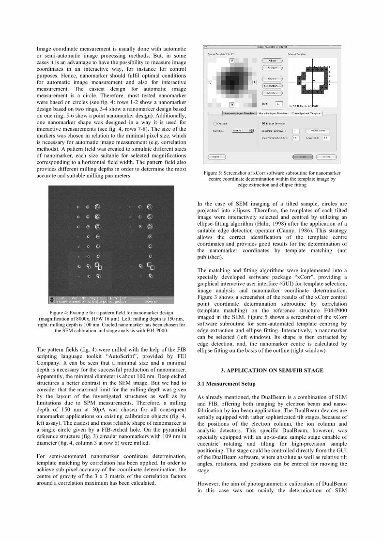
Image coordinate measurement is usually done with automatic or semi-automatic image processing methods. But, in some cases it is an advantage to have the possibility to measure image coordinates in an interactive way, for instance for control purposes. Hence, nanomarker should fulfil optimal conditions for automatic image measurement and also for interactive measurement. The easiest design for automatic image measurement is a circle. Therefore, most tested nanomarker were based on circles (see fig. 4: rows 1-2 show a nanomarker design based on two rings, 3-4 show a nanomarker design based on one ring, 5-6 show a point nanomarker design). Additionally, one nanomarker shape was designed in a way it is used for interactive measurements (see fig. 4, rows 7-8). The size of the markers was chosen in relation to the minimal pixel size, which is necessary for automatic image measurement (e.g. correlation methods). A pattern field was created to simulate different sizes of nanomarker, each size suitable for selected magnifications corresponding to a horizontal field width. The pattern field also provides different milling depths in order to determine the most accurate and suitable milling parameters.
Figure 4: Example for a pattern field for nanomarker design (magnification of 8000x, HFW 16 µm). Left: milling depth is 150 nm, right: milling depth is 100 nm. Circled nanomarker has been chosen for
the SEM calibration and stage analysis with F04-P000.
The pattern fields (fig. 4) were milled with the help of the FIB scripting language toolkit “AutoScript”, provided by FEI Company. It can be seen that a minimal size and a minimal depth is necessary for the successful production of nanomarker. Apparently, the minimal diameter is about 100 nm. Deep etched structures a better contrast in the SEM image. But we had to consider that the maximal limit for the milling depth was given by the layout of the investigated structures as well as by limitations due to SPM measurements. Therefore, a milling depth of 150 nm at 30pA was chosen for all consequent nanomarker applications on existing calibration objects (fig. 4, left assay). The easiest and most reliable shape of nanomarker is a single circle given by a FIB-etched hole. On the pyramidal reference structure (fig. 3) circular nanomarkers with 109 nm in diameter (fig. 4, column 3 at row 6) were milled. For semi-automated nanomarker coordinate determination, template matching by correlation has been applied. In order to achieve sub-pixel accuracy of the coordinate determination, the centre of gravity of the 3 x 3 matrix of the correlation factors around a correlation maximum has been calculated.
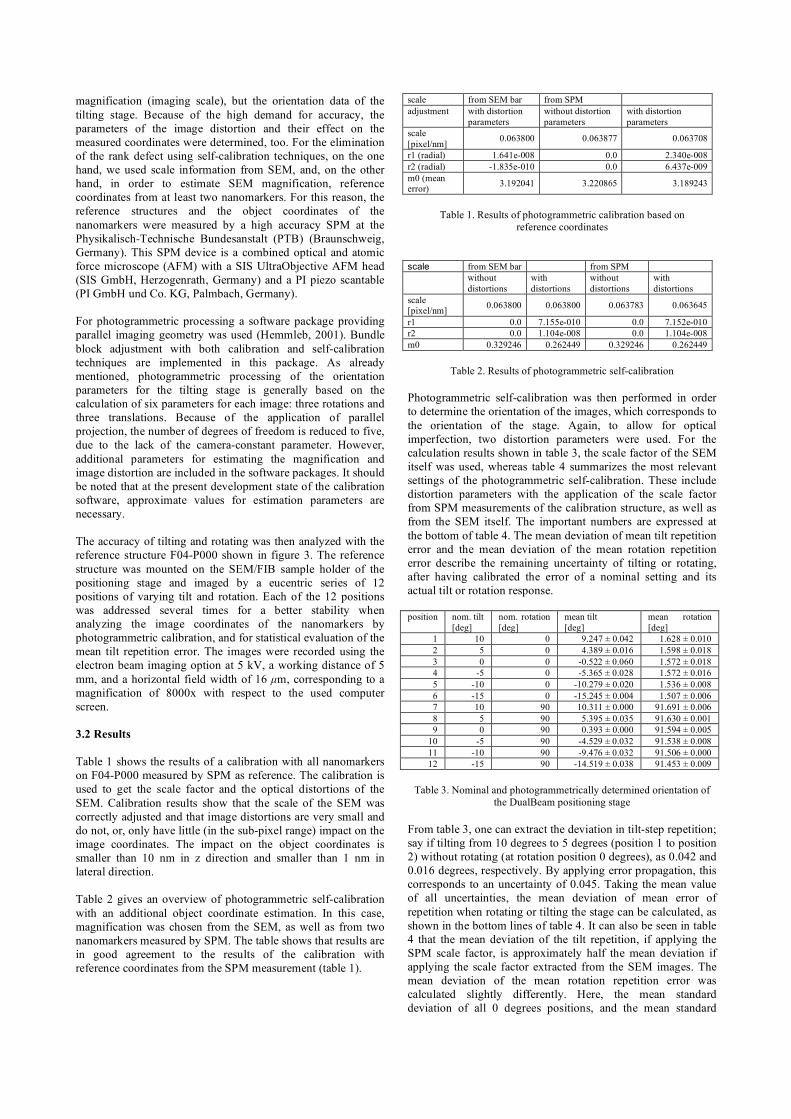
Figure 5: Screenshot of xCorr software subroutine for nanomarker centre coordinate determination within the template image by
edge extraction and ellipse fitting
In the case of SEM imaging of a tilted sample, circles are projected into ellipses. Therefore, the templates of each tilted image were interactively selected and centred by utilizing an ellipse-fitting algorithm (Halir, 1998) after the application of a suitable edge detection operator (Canny, 1986). This strategy allows the correct identification of the template centre coordinates and provides good results for the determination of the nanomarker coordinates by template matching (not published). The matching and fitting algorithms were implemented into a specially developed software package “xCorr”, providing a graphical interactive user interface (GUI) for template selection, image analysis and nanomarker coordinate determination. Figure 3 shows a screenshot of the results of the xCorr control point coordinate determination subroutine by correlation (template matching) on the reference structure F04-P000 imaged in the SEM. Figure 5 shows a screenshot of the xCorr software subroutine for semi-automated template centring by edge extraction and ellipse fitting. Interactively, a nanomarker can be selected (left window). Its shape is then extracted by edge detection, and, the nanomarker centre is calculated by ellipse fitting on the basis of the outline (right window).
3. APPLICATION ON SEM/FIB STAGE 3.1 Measurement Setup As already mentioned, the DualBeam is a combination of SEM and FIB, offering both imaging by electron beam and nano-fabrication by ion beam application. The DualBeam devices are serially equipped with rather sophisticated tilt stages, because of the positions of the electron column, the ion column and analytic detectors. This specific DualBeam, however, was specially equipped with an up-to-date sample stage capable of eucentric rotating and tilting for high-precision sample positioning. The stage could be controlled directly from the GUI of the DualBeam software, where absolute as well as relative tilt angles, rotations, and positions can be entered for moving the stage. However, the aim of photogrammetric calibration of DualBeam in this case was not mainly the determination of SEM
magnification (imaging scale), but the orientation data of the tilting stage. Because of the high demand for accuracy, the parameters of the image distortion and their effect on the measured coordinates were determined, too. For the elimination of the rank defect using self-calibration techniques, on the one hand, we used scale information from SEM, and, on the other hand, in order to estimate SEM magnification, reference coordinates from at least two nanomarkers. For this reason, the reference structures and the object coordinates of the nanomarkers were measured by a high accuracy SPM at the Physikalisch-Technische Bundesanstalt (PTB) (Braunschweig, Germany). This SPM device is a combined optical and atomic force microscope (AFM) with a SIS UltraObjective AFM head (SIS GmbH, Herzogenrath, Germany) and a PI piezo scantable (PI GmbH und Co. KG, Palmbach, Germany). For photogrammetric processing a software package providing parallel imaging geometry was used (Hemmleb, 2001). Bundle block adjustment with both calibration and self-calibration techniques are implemented in this package. As already mentioned, photogrammetric processing of the orientation parameters for the tilting stage is generally based on the calculation of six parameters for each image: three rotations and three translations. Because of the application of parallel projection, the number of degrees of freedom is reduced to five, due to the lack of the camera-constant parameter. However, additional parameters for estimating the magnification and image distortion are included in the software packages. It should be noted that at the present development state of the calibration software, approximate values for estimation parameters are necessary. The accuracy of tilting and rotating was then analyzed with the reference structure F04-P000 shown in figure 3. The reference structure was mounted on the SEM/FIB sample holder of the positioning stage and imaged by a eucentric series of 12 positions of varying tilt and rotation. Each of the 12 positions was addressed several times for a better stability when analyzing the image coordinates of the nanomarkers by photogrammetric calibration, and for statistical evaluation of the mean tilt repetition error. The images were recorded using the electron beam imaging option at 5 kV, a working distance of 5 mm, and a horizontal field width of 16 µm, corresponding to a magnification of 8000x with respect to the used computer screen. 3.2 Results Table 1 shows the results of a calibration with all nanomarkers on F04-P000 measured by SPM as reference. The calibration is used to get the scale factor and the optical distortions of the SEM. Calibration results show that the scale of the SEM was correctly adjusted and that image distortions are very small and do not, or, only have little (in the sub-pixel range) impact on the image coordinates. The impact on the object coordinates is smaller than 10 nm in z direction and smaller than 1 nm in lateral direction. Table 2 gives an overview of photogrammetric self-calibration with an additional object coordinate estimation. In this case, magnification was chosen from the SEM, as well as from two nanomarkers measured by SPM. The table shows that results are in good agreement to the results of the calibration with reference coordinates from the SPM measurement (table 1).
scale from SEM bar from SPM adjustment with distortion
parameters without distortion parameters
with distortion parameters
scale [pixel/nm] 0.063800 0.063877 0.063708
r1 (radial) 1.641e-008 0.0 2.340e-008 r2 (radial) -1.835e-010 0.0 6.437e-009 m0 (mean error) 3.192041 3.220865 3.189243
Table 1. Results of photogrammetric calibration based on
reference coordinates scale from SEM bar from SPM without
distortions with distortions
without distortions
with distortions
scale [pixel/nm] 0.063800 0.063800 0.063783 0.063645
r1 0.0 7.155e-010 0.0 7.152e-010 r2 0.0 1.104e-008 0.0 1.104e-008 m0 0.329246 0.262449 0.329246 0.262449
Table 2. Results of photogrammetric self-calibration Photogrammetric self-calibration was then performed in order to determine the orientation of the images, which corresponds to the orientation of the stage. Again, to allow for optical imperfection, two distortion parameters were used. For the calculation results shown in table 3, the scale factor of the SEM itself was used, whereas table 4 summarizes the most relevant settings of the photogrammetric self-calibration. These include distortion parameters with the application of the scale factor from SPM measurements of the calibration structure, as well as from the SEM itself. The important numbers are expressed at the bottom of table 4. The mean deviation of mean tilt repetition error and the mean deviation of the mean rotation repetition error describe the remaining uncertainty of tilting or rotating, after having calibrated the error of a nominal setting and its actual tilt or rotation response. position nom. tilt
[deg] nom. rotation [deg]
mean tilt [deg]
mean rotation [deg]
1 10 0 9.247 ± 0.042 1.628 ± 0.010 2 5 0 4.389 ± 0.016 1.598 ± 0.018 3 0 0 -0.522 ± 0.060 1.572 ± 0.018 4 -5 0 -5.365 ± 0.028 1.572 ± 0.016 5 -10 0 -10.279 ± 0.020 1.536 ± 0.008 6 -15 0 -15.245 ± 0.004 1.507 ± 0.006 7 10 90 10.311 ± 0.000 91.691 ± 0.006 8 5 90 5.395 ± 0.035 91.630 ± 0.001 9 0 90 0.393 ± 0.000 91.594 ± 0.005
10 -5 90 -4.529 ± 0.032 91.538 ± 0.008 11 -10 90 -9.476 ± 0.032 91.506 ± 0.000 12 -15 90 -14.519 ± 0.038 91.453 ± 0.009
Table 3. Nominal and photogrammetrically determined orientation of
the DualBeam positioning stage From table 3, one can extract the deviation in tilt-step repetition; say if tilting from 10 degrees to 5 degrees (position 1 to position 2) without rotating (at rotation position 0 degrees), as 0.042 and 0.016 degrees, respectively. By applying error propagation, this corresponds to an uncertainty of 0.045. Taking the mean value of all uncertainties, the mean deviation of mean error of repetition when rotating or tilting the stage can be calculated, as shown in the bottom lines of table 4. It can also be seen in table 4 that the mean deviation of the tilt repetition, if applying the SPM scale factor, is approximately half the mean deviation if applying the scale factor extracted from the SEM images. The mean deviation of the mean rotation repetition error was calculated slightly differently. Here, the mean standard deviation of all 0 degrees positions, and the mean standard
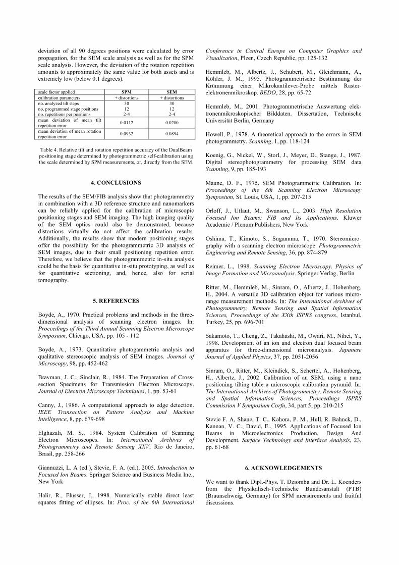
deviation of all 90 degrees positions were calculated by error propagation, for the SEM scale analysis as well as for the SPM scale analysis. However, the deviation of the rotation repetition amounts to approximately the same value for both assets and is extremely low (below 0.1 degrees). scale factor applied SPM SEM calibration parameters + distortions + distortions no. analyzed tilt steps no. programmed stage positions no. repetitions per positions
30 12 2-4
30 12 2-4
mean deviation of mean tilt repetition error 0.0112 0.0280
mean deviation of mean rotation repetition error 0.0932 0.0894
Table 4. Relative tilt and rotation repetition accuracy of the DualBeam positioning stage determined by photogrammetric self-calibration using the scale determined by SPM measurements, or, directly from the SEM.
4. CONCLUSIONS The results of the SEM/FIB analysis show that photogrammetry in combination with a 3D reference structure and nanomarkers can be reliably applied for the calibration of microscopic positioning stages and SEM imaging. The high imaging quality of the SEM optics could also be demonstrated, because distortions virtually do not affect the calibration results. Additionally, the results show that modern positioning stages offer the possibility for the photogrammetric 3D analysis of SEM images, due to their small positioning repetition error. Therefore, we believe that the photogrammetric in-situ analysis could be the basis for quantitative in-situ prototyping, as well as for quantitative sectioning, and, hence, also for serial tomography.
5. REFERENCES Boyde, A., 1970. Practical problems and methods in the three-dimensional analysis of scanning electron images. In: Proceedings of the Third Annual Scanning Electron Microscope Symposium, Chicago, USA, pp. 105 - 112 Boyde, A., 1973. Quantitative photogammetric analysis and qualitative stereoscopic analysis of SEM images. Journal of Microscopy, 98, pp. 452-462 Bravman, J. C., Sinclair, R., 1984. The Preparation of Cross-section Specimens for Transmission Electron Microscopy. Journal of Electron Microscopy Techniques, 1, pp. 53-61 Canny, J., 1986. A computational approach to edge detection. IEEE Transaction on Pattern Analysis and Machine Intelligence, 8, pp. 679-698 Elghazali, M. S., 1984. System Calibration of Scanning Electron Microscopes. In: International Archives of Photogrammetry and Remote Sensing XXV, Rio de Janeiro, Brasil, pp. 258-266 Giannuzzi, L. A (ed.), Stevie, F. A. (ed.), 2005. Introduction to Focused Ion Beams. Springer Science and Business Media Inc., New York Halir, R., Flusser, J., 1998. Numerically stable direct least squares fitting of ellipses. In: Proc. of the 6th International
Conference in Central Europe on Computer Graphics and Visualization, Plzen, Czech Republic, pp. 125-132 Hemmleb, M., Albertz, J., Schubert, M., Gleichmann, A., Köhler, J. M., 1995. Photogrammetrische Bestimmung der Krümmung einer Mikrokantilever-Probe mittels Raster-elektronenmikroskop. BEDO, 28, pp. 65-72 Hemmleb, M., 2001. Photogrammetrische Auswertung elek-tronenmikroskopischer Bilddaten. Dissertation, Technische Universität Berlin, Germany Howell, P., 1978. A theoretical approach to the errors in SEM photogrammetry. Scanning, 1, pp. 118-124 Koenig, G., Nickel, W., Storl, J., Meyer, D., Stange, J., 1987. Digital stereophotogrammetry for processing SEM data Scanning, 9, pp. 185-193 Maune, D. F., 1975. SEM Photogrammetric Calibration. In: Proceedings of the 8th Scanning Electron Microscopy Symposium, St. Louis, USA, 1, pp. 207-215 Orloff, J., Utlaut, M., Swanson, L., 2003. High Resolution Focused Ion Beams: FIB and Its Applications. Kluwer Academic / Plenum Publishers, New York Oshima, T., Kimoto, S., Suganuma, T., 1970. Stereomicro-graphy with a scanning electron microscope. Photogrammetric Engineering and Remote Sensing, 36, pp. 874-879 Reimer, L., 1998. Scanning Electron Microscopy. Physics of Image Formation and Microanalysis. Springer Verlag, Berlin Ritter, M., Hemmleb, M., Sinram, O., Albertz, J., Hohenberg, H., 2004. A versatile 3D calibration object for various micro-range measurement methods. In: The International Archives of Photogrammetry, Remote Sensing and Spatial Information Sciences, Proceedings of the XXth ISPRS congress, Istanbul, Turkey, 25, pp. 696-701 Sakamoto, T., Cheng, Z., Takahashi, M., Owari, M., Nihei, Y., 1998. Development of an ion and electron dual focused beam apparatus for three-dimensional microanalysis. Japanese Journal of Applied Physics, 37, pp. 2051-2056 Sinram, O., Ritter, M., Kleindiek, S., Schertel, A., Hohenberg, H., Albertz, J., 2002. Calibration of an SEM, using a nano positioning tilting table a microscopic calibration pyramid. In: The International Archives of Photogrammetry, Remote Sensing and Spatial Information Sciences, Proceedings ISPRS Commission V Symposium Corfu, 34, part 5, pp. 210-215 Stevie F. A, Shane, T. C., Kahora, P. M., Hull, R. Bahnck, D., Kannan, V. C., David, E., 1995. Applications of Focused Ion Beams in Microelectronics Production, Design And Development. Surface Technology and Interface Analysis, 23, pp. 61-68
6. ACKNOWLEDGEMENTS We want to thank Dipl.-Phys. T. Dziomba and Dr. L. Koenders from the Physikalisch-Technische Bundesanstalt (PTB) (Braunschweig, Germany) for SPM measurements and fruitful discussions.


![RUNNING TIME ANALYSIS - GitHub Pages · Running time analysis of the iterative algorithm function F(n) Create an array fib[1..n] fib[1] = 1 fib[2] = 1 for i = 3 to n: fib[i] = fib[i-1]](https://img.pdfslide.us/doc/110x75/5e95ef9e965d8c2b7e7f1cbb/running-time-analysis-github-pages-running-time-analysis-of-the-iterative-algorithm.jpg)