Embed Size (px)
Citation preview
SEMBODAI RUKMANI VARATHAHARAJAN ENGINEERING COLLEGE
DEPARTMENT OF ELECTRONICS AND COMMUNICATION ENGINEERING
EC6211 CIRCUITS AND DEVICES LABORATORY
Lab manual

EC6211 CIRCUITS AND DEVICES LABORATORY
List of Experiments
1. Verification of KVL & KCL.
2. Verification of Thevenin & Norton’s Theorems.
3. Verification of Superposition Theorem.
4. Verification of Maximum Power Transfer & reciprocity Theorems.
5. Frequency response of series & parallel resonance circuits.
6. Characteristics of PN
7. Characteristics of Zener diode.
8. Characteristics of CE configuration.
9. Characteristics of CB configuration.
10. Characteristics of SCR.
11. Characteristics of JFET & MOSFET.
12. Transient analysis of RL and RC circuits
13. Clipper and Clamper & FWR
KIRCHOFF’S VOLTAGE LAW
EX. NO: 1(a) AIM:
To verify the Kirchoff’s Voltage Law (KVL) for the given circuit.
APPARATUS REQUIRED:
S.NO APPARATUS TYPE RANGE QUANTITY
1 RPS DC (0-30)V 1
2 Resistor - 1KΩ 3
3 Voltmeter DC (0-10)V 3
4 Bread board - - 1
5 Connecting wires - - Few
FORMULA USED:
1. CURRENT DIVISION RULE:
I = TOTAL CURRENT X OPPOSITE RESISTANCE TOTAL RESISTANCE
2. OHM’S LAW:
V=IR
Where, V = Voltage in Volts
I = Current in Amperes
R = Resister in Ohms
THEORY:
KIRCHOFF’S VOLTAGE LAW:
It states that the algebraic sum of all the voltages in a closed loop is equal to
zero.
∑V = 0
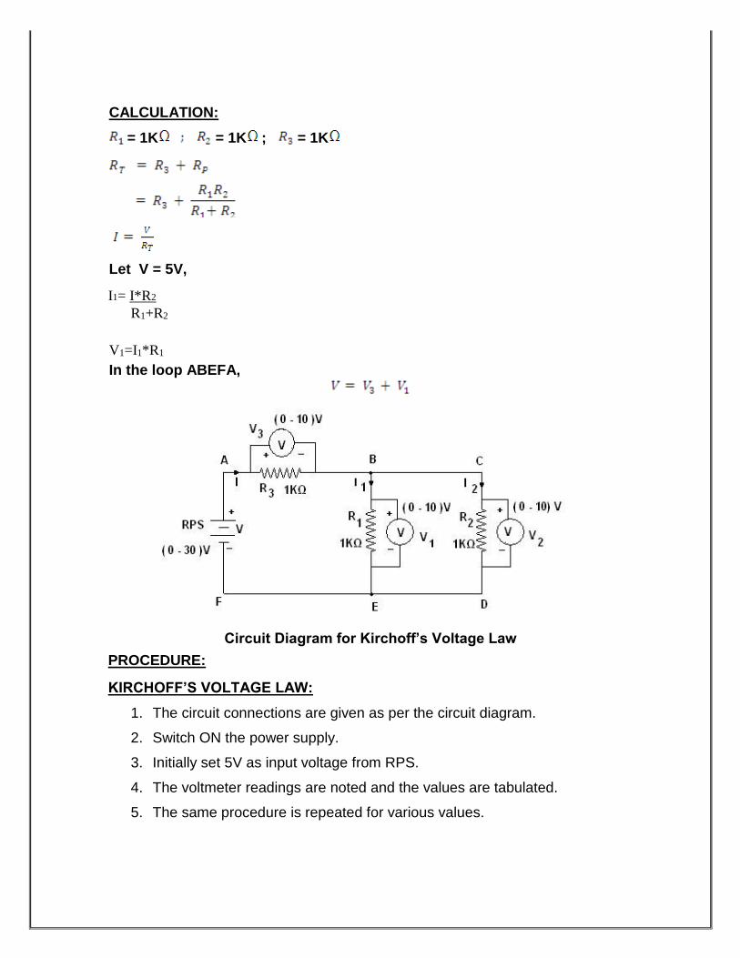
I1= I*R2
R1+R2
V1=I1*R1
PROCEDURE:
KIRCHOFF’S VOLTAGE LAW:
1. The circuit connections are given as per the circuit diagram.
2. Switch ON the power supply.
3. Initially set 5V as input voltage from RPS.
4. The voltmeter readings are noted and the values are tabulated.
5. The same procedure is repeated for various values.
CALCULATION:
= 1K = 1K ; = 1K
Let V = 5V,
In the loop ABEFA,
Circuit Diagram for Kirchoff’s Voltage Law

Table:
Let V = 5V
Resistance in Ohms Vo ltage in Volts V = V1 + V3
= V2 + V3 (V) R1 R2 R3 RT V1 V2 V3
Theoretical
Practical
RESULT:
Thus the Kirchoff’s Voltage Law (KVL) for the given circuit is verified.

KIRCHOFF’S CURRENT LAW
EX. NO: 1(b) AIM:
To verify the Kirchoff’s Current Law (KCL) for the given circuit.
APPARATUS REQUIRED:
S.NO APPARATUS TYPE RANGE QUANTITY
1 RPS DC (0-30)V 1
2 Resistor - 1KΩ 3
3 Ammeter DC (0-30)mA 3
4 Bread board - - 1
5 Connecting wires - - Few
FORMULA USED:
1. CURRENT DIVISION RULE:
I = TOTAL CURRENT X OPPOSITE RESISTANCE TOTAL RESISTANCE
2. OHM’S LAW:
Where, V = Voltage in Volts
I = Current in Amperes
R = Resister in Ohms
THEORY:
KIRCHOFF’S CURRENT LAW:
It states that the algebraic sum of the currents meeting at a node is equal
to zero.
CALCULATION:
= 1K = 1K ; = 1K
I1= I*R2
R1+R2
At node B the current = I=I1+I2
Circuit Diagram for Kirchoff’s Current Law
PROCEDURE:
KIRCHOFF’S CURRENT LAW:
1. The circuit connections are given as per the circuit diagram.
2. Switch ON the power supply.
3. Initially set 5V as input voltage from RPS.
4. The ammeter readings are noted and the values are tabulated.
5. The same procedure is repeated for various values.
Let V = 5V,

Table:
Let V = 5V , So I = 3.3 mA
Resistance in Ohms Current in mA
R1 R2 R3 RT I1 I2 I = I1+I2
Theoritical
Practical
RESULT:
Thus the Kirchoff’s Current Law (KCL) for the given circuit is verified.

THEVENIN’S THEOREM
EX. NO: 2(a)
AIM:
To verify the Thevenin’s theorem for the given circuit. APPARATUS REQUIRED:
S.NO APPARATUS TYPE RANGE QUANTITY
1 RPS DC (0-30)V 1
2 Resistor - 1KΩ 3
3 Ammeter DC (0-10)mA 1
4 Bread board - - 1
5 Connecting wires - - Few
THEORY:
THEVENIN’S THEOREM:
Any linear active network with output terminals C and D can be replaced by a
single voltage source (VTh = VOc) in series with a single impedance (ZTh =
Zi).
VTh is the Thevenin’s voltage. It is the voltage between the terminals C and D on
open circuit condition. Hence it is called open circuit voltage denoted by
VOc.
ZTh is called Thevenin’s impedance. It is the driving point impedance at the
terminals C and D when all the internal sources are set to zero. In case of DC ZTh is
replaced by RTh.
Circuit Diagram for Thevenin’s Theorem
CALCULATION:
The Thevenin’s equivalent circuit is,
R1+R2
To Find R TH :
= 1K = 1K ;
R TH = R 1 *R 2
To Find VTH:
Let V = 5V,
VTH=VBE
PROCEDURE:
1. The circuit connections are given as per the circuit diagram.
2. Switch ON the power supply.
3. Initially set 5V as input voltage from RPS.
4. The ammeter reading is noted and the value is tabulated.
Table: Let V =5V
S.No Voltage in Volts Load Current in Amps
Theoretical Value Practical Value
1 5
RESULT:

Thus the Thevenin’s theorem for the given circuit is verified succe
NORTON’S THEOREM
EX. NO: 2(b)
AIM:
To verify the Norton’s theorem for the given circuit. APPARATUS REQUIRED:
S.NO APPARATUS TYPE RANGE QUANTITY
1 RPS DC (0-30)V 1
2 Resistor - 1KΩ 3
3 Ammeter DC (0-10)mA 1
4 Bread board - - 1
5 Connecting wires - - Few
THEORY:
NORTON’S THEOREM:
Any linear active network with output terminals C and D can be replaced by a
single current source ISC(IN) in parallel with a single impedance (ZTh = Zn).
ISC is the current through the terminals C and D on short circuit condition.
ZTh is called Thevenin’s impedance. In case of DC ZTh is replaced by RTh.
The current through impedance connected to the terminals of the Norton’s
equivalent circuit must have the same direction as the current through the same
impedance connected to the original active network.
Circuit Diagram for Norton’s Theorem

CALCULATION:
R1+R2
To Find ISC:
The Norton’s equivalent circuit is,
To Find R TH :
= 1K 1K = ;
R TH = R 1 *R 2

Let V=5V
RTH+RL
PROCEDURE:
1. The circuit connections are given as per the circuit diagram.
2. Switch ON the power supply.
3. Initially set 5V as input voltage from RPS.
4. The ammeter reading is noted and the value is tabulated.
In the loop ABEFA by applying KVL,
In the loop BCDEB by applying KVL,
From the equation (I) and (2),
∴
I L = I SC *R TH

Table: Let V =5V
ISC IL
Theoritical
Practical
RESULT:
Thus the Norton’s theorem for the given circuit is verified success
SUPERPOSITION THEOREM
EX. NO: 3
AIM:
To verify the superposition theorem for the given circuit. APPARATUS REQUIRED:
S.NO APPARATUS TYPE RANGE QUANTITY
1 RPS DC (0-30)V 2
2 Resistor - 1KΩ 3
3 Ammeter DC (0-10)mA 1
4 Bread board - - 1
5 Connecting wires - - Few
THEORY:
SUPERPOSITION THEOREM:
The superposition theorem for electrical circuits states that the total current
in any branch of a bilateral linear circuit equals the algebraic sum of the currents
produced by each source acting separately throughout the circuit.
To ascertain the contribution of each individual source, all of the other sources first must
be "killed" (set to zero) by:
1. replacing all other voltage sources with a short circuit (thereby eliminating difference
of potential. i.e. V=0)
2. replacing all other current sources with an open circuit (thereby eliminating current.
i.e. I=0)
This procedure is followed for each source in turn, and then the resultant
currents are added to determine the true operation of the circuit. The resultant
circuit operation is the superposition of the various voltage and current sources.
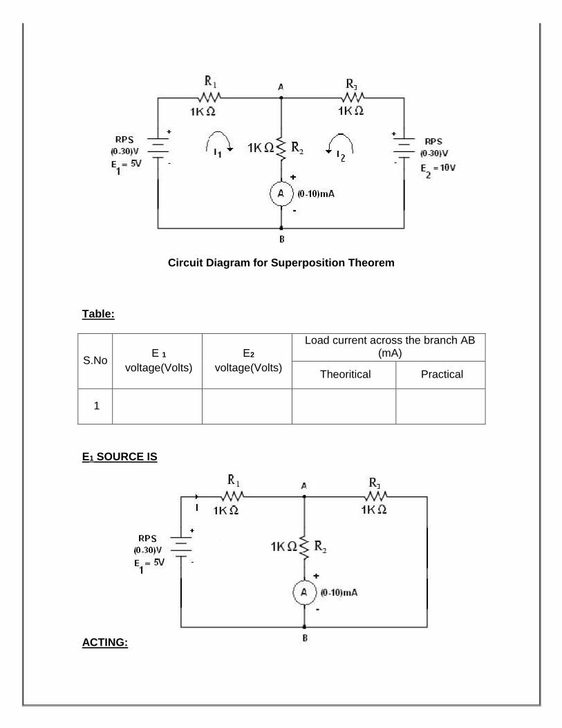
Circuit Diagram for Superposition Theorem
Table:
S.No E 1
voltage(Volts)
E2
voltage(Volts)
Load current across the branch AB (mA)
Theoritical Practical
1
E1 SOURCE IS
ACTING:
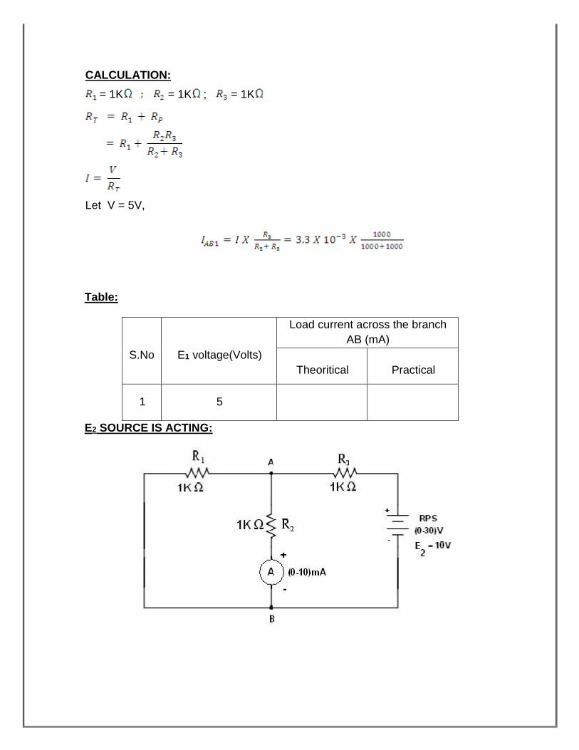
Table:
S.No E1 voltage(Volts)
Load current across the branch
AB (mA)
Theoritical Practical
1 5
E2 SOURCE IS ACTING:
CALCULATION:
= 1K = 1K ; = 1K
Let V = 5V,
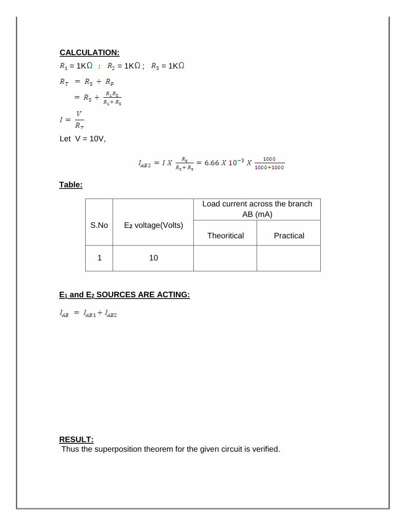
Table:
S.No E2 voltage(Volts)
Load current across the branch
AB (mA)
Theoritical Practical
1 10
E1 and E2 SOURCES ARE ACTING:
RESULT:
Thus the superposition theorem for the given circuit is verified.
CALCULATION:
= 1K = 1K ; = 1K
Let V = 10V,

MAXIMUM POWER TRANSFER THEOREM
EX. NO: 4(a)
AIM:
To verify the maximum power transfer theorem for the given circuit. APPARATUS REQUIRED:
S.NO APPARATUS TYPE RANGE QUANTITY
1 RPS DC (0-30)V 1
2 Resistor - 1KΩ 2
3 Variable Resistor 1KΩ 1
4 Ammeter DC (0-10)mA 1
5 Bread board - - 1
6 Connecting wires - - Few
THEORY:
MAXIMUM POWER TRANSFER THEOREM:
In electrical engineering, the maximum power (transfer) theorem states
that, to obtain maximum external power from a source to a load with a finite internal
resistance, the resistance of the load must be made the same as that of the source.
The theorem applies to maximum power, and not maximum efficiency. If the
resistance of the load is made larger than the resistance of the source, then
efficiency is higher, since most of the power is generated in the load, but the overall
power is lower since the total circuit resistance goes up.
If the internal impedance is made larger than the load then most of the power
ends up being dissipated in the source, and although the total power dissipated is
higher, due to a lower circuit resistance, it turns out that the amount dissipated in
the load is reduced.

Circuit Diagram for Maximum Power Transfer Theorem CALCULATION:
To Find R TH :
= 1K = 1K ;
To Find V TH :

1. The circuit connections are given as per the circuit diagram.
2. Switch ON the power supply.
3. Initially set 5V as input voltage from RPS.
4. The ammeter reading is noted for various values of load resistance and the
values are tabulated.
5. The load resistance for the maximum power is obtained from the table.
Table: Let V = 5V
S.No Resistance(RL)
in Ohms
Current(IL)
in mA
Power (IL
2RL) in mW
1 100
2 200
3 300
4 400
5 500
6 700
7 900
RESULT:
Thus the maximum power transfer theorem for the given circuit is verified successfully.
Let V = 5V,
PROCEDURE:

RECIPROCITY THEOREM
EX. NO: 4(b)
AIM:
To verify the reciprocity theorem for the given circuit. APPARATUS REQUIRED:
S.NO APPARATUS TYPE RANGE QUANTITY
1 RPS DC (0-30)V 1
2 Resistor - 1KΩ 4
3 Ammeter DC (0-5)mA 1
4 Bread board - - 1
5 Connecting wires - - Few
THEORY:
RECIPROCITY THEOREM:
The reciprocity theorem states that if an emf ‘E’ in one branch of a reciprocal
network produces a current I in another, then if the emf ‘E’ is moved from the first
to the second branch, it will cause the same current in the first branch, where the
emf has been replaced by a short circuit. We shall see that any network composed
of linear, bilateral elements (such as R, L and C) is reciprocal.
Before interchanging:
Circuit Diagram for Reciprocity Theorem
CALCULATION:
Let V=5V

PROCEDURE:
1. The circuit connections are given as per the circuit diagram.
2. Switch ON the power supply.
3. Initially set 5V as input voltage from RPS.
4. The ammeter reading is noted and tabulated.
Table for before interchanging:
V (Volts) Current (mA)
Theoritical Practical
5
In the loop ABEF by applying KVL,
In the loop BCDE by applying KVL,
D =
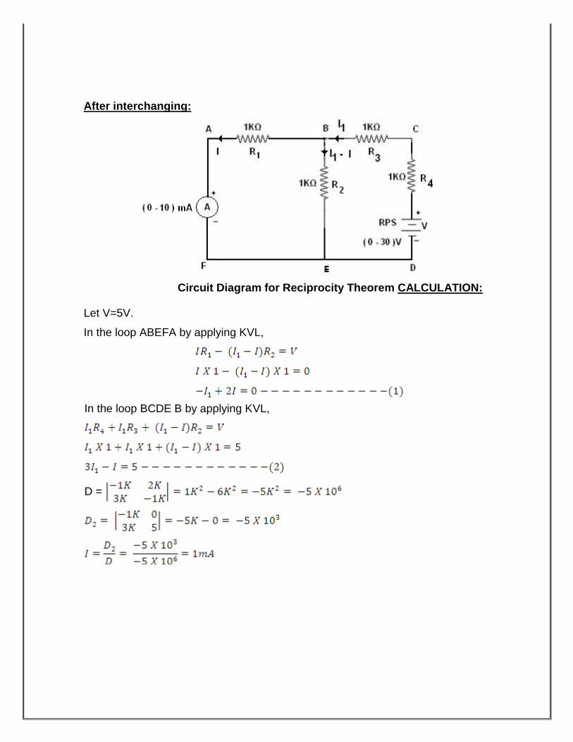
After interchanging:
Circuit Diagram for Reciprocity Theorem CALCULATION:
Let V=5V.
In the loop ABEFA by applying KVL,
In the loop BCDE B by applying KVL,
D =

PROCEDURE:
1. The circuit connections are given as per the circuit diagram.
2. Switch ON the power supply.
3. Initially set 5V as input voltage from RPS.
4. The ammeter reading is noted and tabulated.
Table for before interchanging:
V (Volts) Current (mA)
Theoritical Practical
5
RESULT:
Thus the reciprocity theorem for the given circuit is verified successfully.
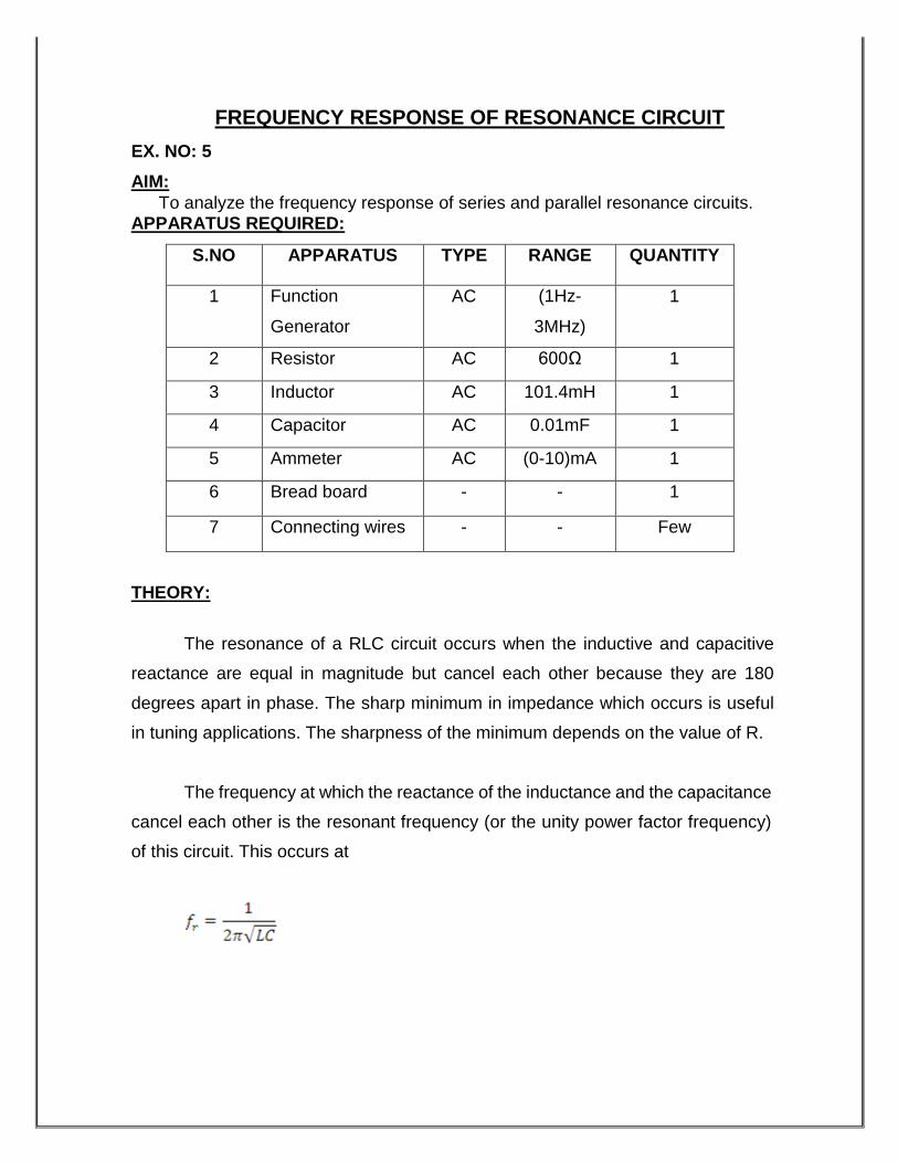
FREQUENCY RESPONSE OF RESONANCE CIRCUIT
EX. NO: 5
AIM:
To analyze the frequency response of series and parallel resonance circuits. APPARATUS REQUIRED:
S.NO APPARATUS TYPE RANGE QUANTITY
1 Function
Generator
AC (1Hz-
3MHz)
1
2 Resistor AC 600Ω 1
3 Inductor AC 101.4mH 1
4 Capacitor AC 0.01mF 1
5 Ammeter AC (0-10)mA 1
6 Bread board - - 1
7 Connecting wires - - Few
THEORY:
The resonance of a RLC circuit occurs when the inductive and capacitive
reactance are equal in magnitude but cancel each other because they are 180
degrees apart in phase. The sharp minimum in impedance which occurs is useful
in tuning applications. The sharpness of the minimum depends on the value of R.
The frequency at which the reactance of the inductance and the capacitance
cancel each other is the resonant frequency (or the unity power factor frequency)
of this circuit. This occurs at

SERIES RESONANCE:
Circuit Diagram for Series Resonant CALCULATION:
R = 600Ω
L = 101.4mH
C = 0.01µF
PROCEDURE:
1. The circuit connections are given as per the circuit diagram.
2. Switch ON the power supply.
3. The input is given in the form of sin wave by function generator.
4. The amplitude of the response across the resistor is noted for various
frequency ranges.
5. The current is calculated and tabulated.
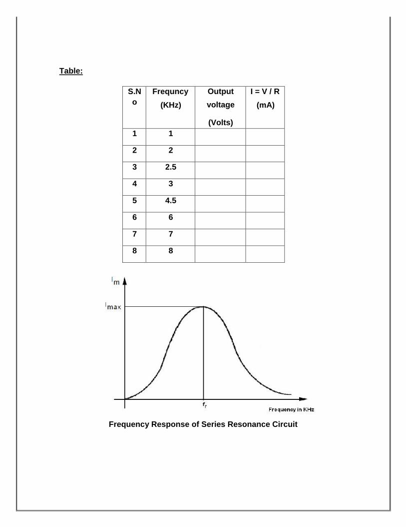
Table:
S.N
o
Frequncy
(KHz)
Output
voltage
(Volts)
I = V / R
(mA)
1 1
2 2
3 2.5
4 3
5 4.5
6 6
7 7
8 8
Frequency Response of Series Resonance Circuit

PARALLEL RESONANCE:
Circuit Diagram for Parallel Resonant
CALCULATION:
R = 600Ω
L = 101.4mH
C = 0.01µF
PROCEDURE:
1. The circuit connections are given as per the circuit diagram.
2. Switch ON the power supply.
3. The input is given in the form of sin wave by function generator.
4. The amplitude of the response across the resistor is noted for various frequency
ranges.
5. The current is calculated and tabulated.
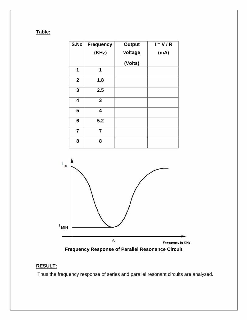
Table:
S.No Frequency
(KHz)
Output
voltage
(Volts)
I = V / R
(mA)
1 1
2 1.8
3 2.5
4 3
5 4
6 5.2
7 7
8 8
Frequency Response of Parallel Resonance Circuit
RESULT:
Thus the frequency response of series and parallel resonant circuits are analyzed.

CHARACTERISTICS OF PN DIODE
EX. NO: 6 AIM:
To determine the forward and reverse characteristics of a PN diode.
APPARATUS REQUIRED:
S.NO APPARATUS RANGE QUANTITY
1 RPS (0-30)V 1
2 Resistor 220Ω 1
3 DC Voltmeter (0-1)V 1
4 DC Ammeter (0-100)mA 1
5 Diode IN4007 1
6 Bread board - 1
7 Connecting wires - Few
THEORY: V-I
Characteristic equation or diode current equation is,
A semiconductor diode's current–voltage characteristic, or I–V curve, is related
to the transport of carriers through the so-called depletion layer or depletion region
that exists at the p-n junction between differing semiconductors.
If an external voltage is placed across the diode, an increasing electric field
develops through the depletion zone which acts to slow and then finally stop
recombination. At this point, there is a "built-in" potential across the depletion
zone.
If an external voltage across the diode with the same polarity as the builtin
potential, the depletion zone continues to act as an insulator, preventing any
significant electric current flow. This is the reverse bias phenomenon.
However, if the polarity of the external voltage opposes the built-in
potential, recombination can once again proceed, resulting in substantial electric
current through the p-n junction. For silicon diodes, the built-in potential is
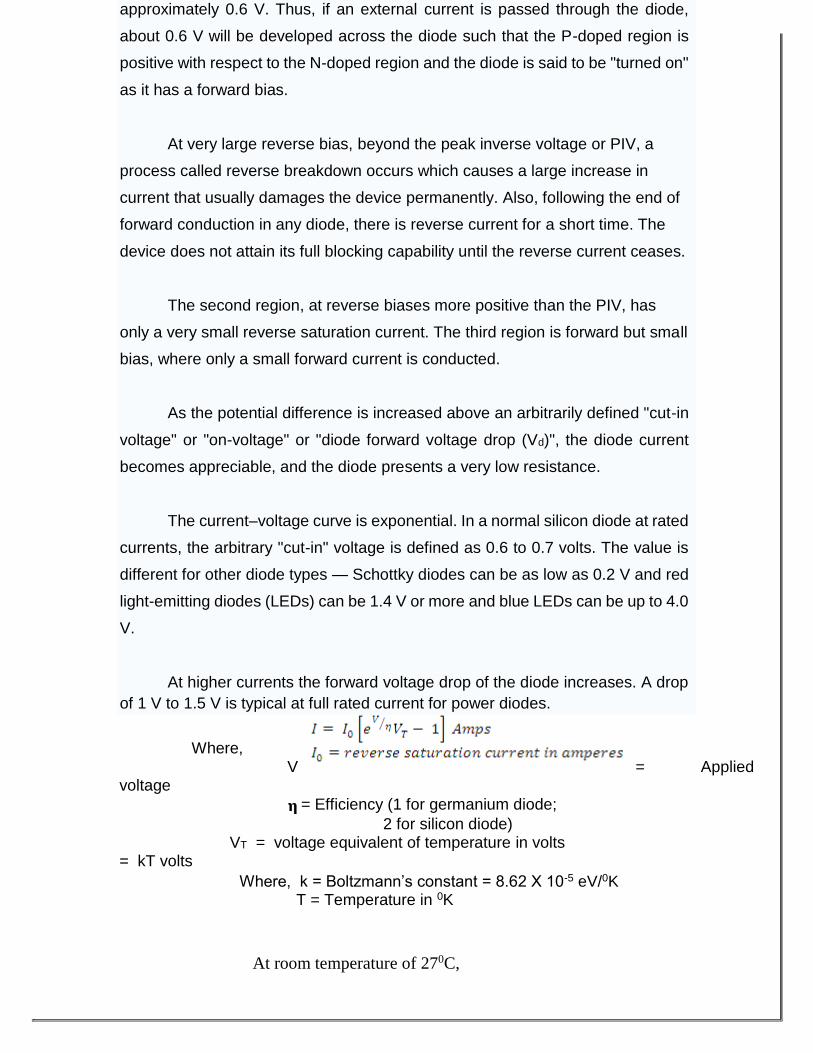
Where, V = Applied voltage
= Efficiency (1 for germanium diode;
2 for silicon diode) VT = voltage equivalent of temperature in volts = kT volts
Where, k = Boltzmann’s constant = 8.62 X 10⁻⁵ eV/0K T = Temperature in 0K
approximately 0.6 V. Thus, if an external current is passed through the diode,
about 0.6 V will be developed across the diode such that the P-doped region is
positive with respect to the N-doped region and the diode is said to be "turned on"
as it has a forward bias.
At very large reverse bias, beyond the peak inverse voltage or PIV, a
process called reverse breakdown occurs which causes a large increase in
current that usually damages the device permanently. Also, following the end of
forward conduction in any diode, there is reverse current for a short time. The
device does not attain its full blocking capability until the reverse current ceases.
The second region, at reverse biases more positive than the PIV, has
only a very small reverse saturation current. The third region is forward but small
bias, where only a small forward current is conducted.
As the potential difference is increased above an arbitrarily defined "cut-in
voltage" or "on-voltage" or "diode forward voltage drop (Vd)", the diode current
becomes appreciable, and the diode presents a very low resistance.
The current–voltage curve is exponential. In a normal silicon diode at rated
currents, the arbitrary "cut-in" voltage is defined as 0.6 to 0.7 volts. The value is
different for other diode types — Schottky diodes can be as low as 0.2 V and red
light-emitting diodes (LEDs) can be 1.4 V or more and blue LEDs can be up to 4.0
V.
At higher currents the forward voltage drop of the diode increases. A drop
of 1 V to 1.5 V is typical at full rated current for power diodes.
At room temperature of 270C,
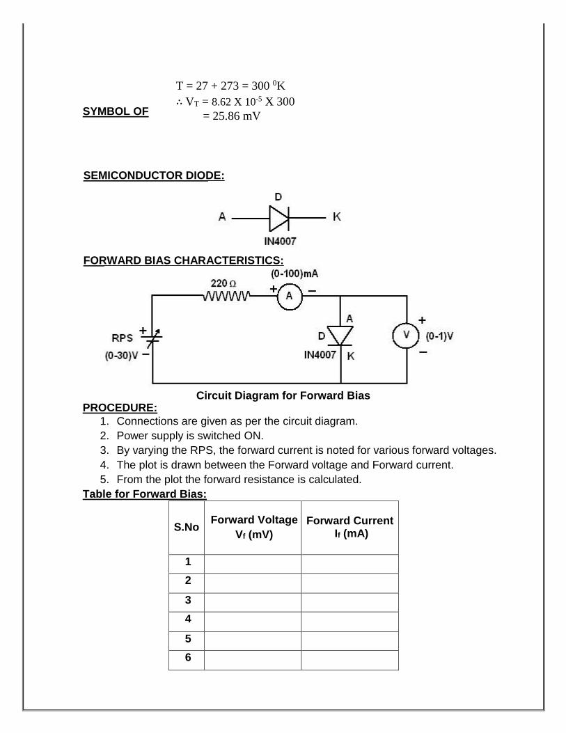
SYMBOL OF
PROCEDURE:
1. Connections are given as per the circuit diagram.
2. Power supply is switched ON.
3. By varying the RPS, the forward current is noted for various forward voltages.
4. The plot is drawn between the Forward voltage and Forward current.
5. From the plot the forward resistance is calculated.
Table for Forward Bias:
S.No Forward Voltage
Vf (mV)
Forward Current
If (mA)
1
2
3
4
5
6
T = 27 + 273 = 300 0K
∴ VT = 8.62 X 10-5 X 300
= 25.86 mV
SEMICONDUCTOR DIODE:
FORWARD BIAS CHARACTERISTICS:
Circuit Diagram for Forward Bias
7
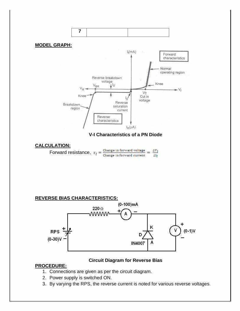
MODEL GRAPH:
V-I Characteristics of a PN Diode
CALCULATION:
Forward resistance,
REVERSE BIAS CHARACTERISTICS:
Circuit Diagram for Reverse Bias
PROCEDURE:
1. Connections are given as per the circuit diagram.
2. Power supply is switched ON.
3. By varying the RPS, the reverse current is noted for various reverse voltages.

4. The plot is drawn between the reverse voltage and reverse current.
5. From the plot the reverse resistance is calculated.
Table for Reverse Bias:
S.No Reverse Voltage
Vr (mV)
Reverse Current
Ir (mA)
1
2
3
4
5
6
7
8
CALCULATION:
(i) Reverse resistance,
RESULT:
Thus the V-I characteristics of a PN diode is drawn for both forward and reverse bias condition.
CHARACTERISTICS OF ZENER DIODE
EX. NO: 7
AIM:
To determine the forward and reverse characteristics of a zener diode.
APPARATUS REQUIRED:
S.NO APPARATUS RANGE QUANTITY
1 RPS (0-30)V 1
2 Resistor 220Ω 1
3 DC Voltmeter (0-1)V 1
4 DC Ammeter (0-100)mA 1
5 Zener Diode IN4730 1
6 Bread board - 1
7 Connecting wires - Few
THEORY:
Zener diode is a special diode with increased amounts of doping. This is to
compensate for the damage that occurs in the case of a pn junction diode when the
reverse bias exceeds the breakdown voltage and thereby current increases at a
rapid rate.
Applying a positive potential to the anode and a negative potential to the
cathode of the zener diode establishes a forward bias condition. The forward
characteristic of the zener diode is same as that of a pn junction diode i.e. as the
applied potential increases the current increases exponentially. Applying a negative
potential to the anode and positive potential to the cathode reverse biases the zener
diode.

As the reverse bias increases the current increases rapidly in a direction
opposite to that of the positive voltage region. Thus under reverse bias condition
breakdown occurs. It occurs because there is a strong electric filed in the region of
the junction that can disrupt the bonding forces within the atom and generate
carriers. The breakdown voltage depends upon the amount of doping. For a heavily
doped diode depletion layer will be thin and breakdown occurs at low reverse
voltage and the breakdown voltage is sharp. Whereas a lightly doped diode has a
higher breakdown voltage. This explains the zener diode characteristics in the
reverse bias region.
SYMBOL OF ZENER DIODE:
FORWARD BIAS CHARACTERISTICS:
Circuit Diagram for Forward Bias PROCEDURE:
1. Connections are given as per the circuit diagram.
2. Power supply is switched ON.
3. By varying the RPS, the forward current is noted for various forward voltages.
4. The plot is drawn between the Forward voltage and Forward current.
5. From the plot the forward resistance is calculated.

Table for Forward Bias:
S.No Forward Voltage
Vf (mV)
Forward Current
If (mA)
1
2
3
4
5
6
7
8
MODEL GRAPH:
Forward Characteristics of a Zener Diode
CALCULATION:
Forward resistance,

REVERSE BIAS CHARACTERISTICS:
Circuit Diagram for Reverse Bias
PROCEDURE:
1. Connections are given as per the circuit diagram.
2. Power supply is switched ON.
3. By varying the RPS, the reverse current is noted for various reverse voltages.
4. The plot is drawn between the reverse voltage and reverse current.
5. From the plot the reverse resistance is calculated.
Table for Reverse Bias:
S.No Reverse Voltage
Vr (mV)
Reverse Current
Ir (mA)
1
2
3
4
5
6
7
8
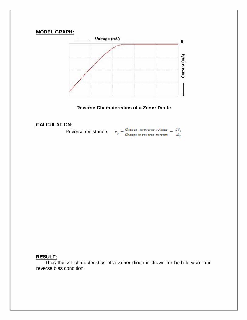
MODEL GRAPH:
Reverse Characteristics of a Zener Diode
CALCULATION:
Reverse resistance,
RESULT:
Thus the V-I characteristics of a Zener diode is drawn for both forward and reverse bias condition.

CHARACTERISTICS OF BJT IN CE CONFIGURATION
EX. NO : 8 AIM:
To plot the input and output characteristics of a bipolar junction transistor (BJT) in
common emitter (CE) configuration.
APPARATUS REQUIRED:
S.NO APPARATUS RANGE QUANTITY
1 RPS (0-30)V 2
2 Resistor 1KΩ 2
3 DC Voltmeter (0-30)V 1
4 DC Voltmeter (0-10)V 1
5 DC Ammeter (0-50)µA 1
6 DC Ammeter (0-30)mA 1
7 BJT BC547 1
8 Bread board - 1
9 Connecting wires - Few
THEORY:
Pin Diagram of BJT Symbol of BJT
The input is applied between emitter and base and output is taken from the
collector and emitter. Here, emitter of the transistor is common to both input and
output circuits and hence the name common emitter (CE) configuration.

Regardless of circuit configuration, the base emitter junction is always
forward biased while the collector-base junction is always reverse biased, to
operate transistor in active region.
Circuit Diagram for a BJT in CE Configuration
INPUT CHARACTERISTICS:
PROCEDURE:
1. Connections are given as per the circuit diagram.
2. The supply is switched ON.
3. The collector-emitter voltage VCE is kept constant.
4. By varying the emitter-base voltage VBE, the various base current IB is noted.
5. The same procedure is repeated for various collector-emitter voltages
VCE.
6. The input characteristic is the curve between input current IB and input voltage
VBE at constant collector-emitter voltage VCE. The base current is taken along Y-
axis and base-emitter voltage along X-axis.
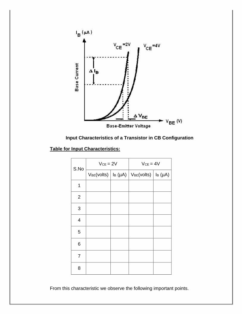
Input Characteristics of a Transistor in CB Configuration
Table for Input Characteristics:
S.No VCE = 2V VCE = 4V
VBE(volts) IB (µA) VBE(volts) IB (µA)
1
2
3
4
5
6
7
8
From this characteristic we observe the following important points.

1. As the input to a transistor in the CE configuration is between the base-
to-emitter junctions, the CE input characteristics resembles a family of
forward-biased diode curves.
2. After the cut-in voltage (barrier potential, normally 0.7 V for silicon and
0.3 V for Germanium), the base current (IB) increases rapidly with small
increase in emitter-base voltage (VEB). It means that input resistance is
very small. Because input resistance is a ratio of change in emitter-base
voltage (∆VEB) to the resulting changes in base current (∆IB) at constant
collector-emitter voltage (VCE), this resistance is also known as the
dynamic input resistance of the transistor in CE configuration.
3. For a fixed value of VBE, IB decreases as VCE is increased. A larger value
of VCE results in a large reverse bias at collector-base p-n junction. This
increases the depletion region and reduces the effective width of the
base. Hence, there are fewer recombinations in the base region,
reducing the base current IB.
OUTPUT CHARACTERISTICS:
PROCEDURE:
1. Connections are given as per the circuit diagram.
2. The supply is switched ON.
3. The base current IB is kept constant.
4. By varying the collector-emitter voltage VCE, the various collector current IC is
noted.
5. The same procedure is repeated for various base current IB.
6. The output characteristic is the curve between collector current IC and collector
emitter voltage VCE at constant base current IB. The collector current is taken
along Y-axis and collector-emitter voltage magnitude along X-axis.
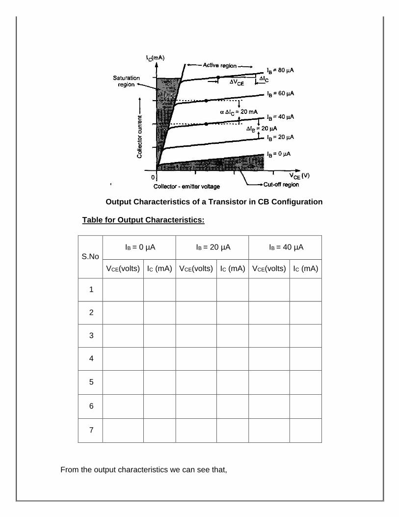
Output Characteristics of a Transistor in CB Configuration
Table for Output Characteristics:
S.No
IB = 0 µA IB = 20 µA IB = 40 µA
VCE(volts) IC (mA) VCE(volts) IC (mA) VCE(volts) IC (mA)
1
2
3
4
5
6
7
From the output characteristics we can see that,
1. The change in collector-emitter voltage (∆VCE) causes the little change in the
collector current (∆IC) for constant base current IB.
2. The output characteristic of common emitter configuration consists of three
regions: Active, Saturation, and cut-off.
3. Active region: The region where the curves are approximately horizontal is
the “active” region of the CE configuration. In the active region, the collector
junction is reverse biased. As VCE is increased, reverse bias increases. This
causes depletion region to spread more in base than in collector, reducing
the chances of recombination in the base.
4. Saturation region : If VCE is reduced to a small value such as 0.2 V, then
collector-base junction becomes forward biased, since the emitter base
junction is already forward biased by 0.7 V. The input junction in CE
configuration is base to emitter junction, which is always forward biased to
operate transistor in active region. Thus input characteristics of CE
configuration are similar to forward characteristics of p-n junction diode.
When both the junctions are forward biased, the transistor operates in the
saturation region, which is indicated on the output characteristics. The
saturation value of VCE, designated VCE (sat) usually ranges between 0.1 V
to 0.3 V.
5. Cut-off region: When the input base current is made equal to zero, the
collector current is the reverse leakage current. Accordingly, in order to cut-
off the transistor, it is not enough to reduce IB = 0. Instead, it is necessary to
reverse bias the emitter junction slightly. We shall define cutoff as the
condition where the collector current is equal to reverse saturation current
and the emitter current is zero.
RESULT:
Thus the input and output characteristics of a bipolar junction transistor in common
emitter configuration is analyzed.

EX. NO : 9 CHARACTERISTICS OF BJT IN CB CONFIGURATION AIM:
To plot the input and output characteristics of a bipolar junction transistor (BJT) in
common base (CB) configuration.
APPARATUS REQUIRED:
S.NO APPARATUS RANGE QUANTITY
1 RPS (0-30)V 2
2 Resistor 1KΩ 2
3 DC Voltmeter (0-30)V 2
4 DC Ammeter (0-10)mA 1
5 DC Ammeter (0-30)mA 1
6 BJT BC547 1
7 Bread board - 1
8 Connecting wires - Few
THEORY:
Pin Diagram of BJT Symbol of BJT
The input is applied between emitter and base and output is taken from the
collector and base. Here, base of the transistor is common to both input and output
circuits and hence the name common base configuration.

Regardless of circuit configuration, the base emitter junction is always
forward biased while the collector-base junction is always reverse biased, to
operate transistor in active region.
Circuit Diagram for a BJT in CB Configuration
INPUT CHARACTERISTICS:
PROCEDURE:
1. Connections are given as per the circuit diagram.
2. The supply is switched ON.
3. The collector-base voltage VCB is kept constant.
4. By varying the emitter-base voltage VEB, the various emitter current
IE is noted.
5. The same procedure is repeated for various collector-base voltages
VCB.
6. The input characteristic is the curve between input current IE and input voltage
VEB at constant collector-base voltage VCB. The emitter current is taken along
Y-axis and emitter base voltage along X-axis.
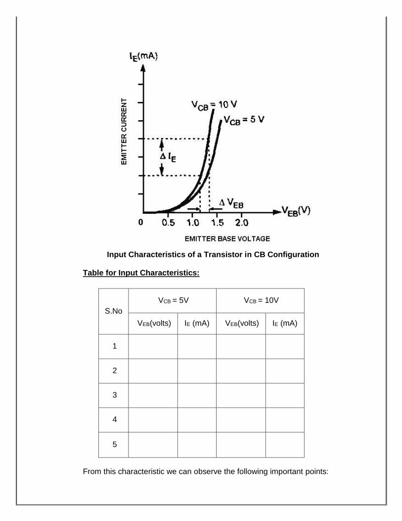
Input Characteristics of a Transistor in CB Configuration
Table for Input Characteristics:
S.No
VCB = 5V VCB = 10V
VEB(volts) IE (mA) VEB(volts) IE (mA)
1
2
3
4
5
From this characteristic we can observe the following important points:

1. After the cut-in voltage (barrier potential, normally 0.7 V for silicon and
0.3 V for Germanium), the emitter current (IE) increases rapidly with small increase
in emitter-base voltage (VEB). It means that input resistance is very small. Because
input resistance is a ratio of change in emitter-base voltage (∆VEB) to the resulting
changes in emitter current (∆IE) at constant collector-base voltage (VCB), this
resistance is also known as the dynamic input resistance of the transistor in CB
configuration.
2. It can be observed that there is slight increase in emitter current (IE) with
increase in VCB. This is due to change in the width of the depletion region in the
base region under the reverse biased condition.
OUTPUT CHARACTERISTICS:
PROCEDURE:
1. Connections are given as per the circuit diagram.
2. The supply is switched ON.
3. The emitter current IE is kept constant.
4. By varying the collector-base voltage VCB, the various collector current IC is
noted.
5. The same procedure is repeated for various emitter current IE.
6. The output characteristic is the curve between collector current IC and
collector base voltage VCB at constant emitter current IE. The collector current
is taken along Y-axis and collector-base voltage magnitude along X-axis.


1. The output characteristic has three basic regions: Active, cut-off and saturation.
State Emitter Base Junction Collector Base Junction
Active Forward Biased Reverse Biased
Cut-off Reverse Biased Reverse Biased
Saturation Forward Biased Forward Biased
2. In active region, IC is approximately equal to IE and transistor works as an
amplifier.
3. The region below the curve IE = 0 is called as cut-off region.
4. The saturation region is that region of the characteristics which is to the left of
VCB =0 V. The exponential increase in collector current as the voltage VCB
increases towards 0 V.
5. As IE increases IC also increases. Thus, IC depends upon input current IE but not
on collector voltage. Hence, input current controls output current. Since
transistor requires some current to drive it, it is called current operating device.
RESULT:
Thus the input and output characteristics of a bipolar junction transistor in common base
configuration is analyzed.
CHARACTERISTICS OF SCR
EX. NO: 10 AIM:

To study and plot the forward and reverse characteristics of silicon controlled
rectifier (SCR).
APPARATUS REQUIRED:
S.NO APPARATUS RANGE QUANTITY
1 RPS (0-30)V 2
2 Resistor 1KΩ 2
3 DC Voltmeter (0-10)V 1
4 DC Ammeter (0-30)mA 2
5 DC Ammeter (0-3)mA 1
6 SCR 2P4M 1
7 Bread board - 1
8 Connecting wires - Few
THEORY:
Pin Diagram of SCR Symbol of SCR
The SCR is a unidirectional device has two states, ON or OFF, and it
allows current to flow in only one direction.
SCR's can remain in the OFF state even though the applied potential
may be several thousand volts. In the ON state, they can pass several
thousand amperes. When a small signal is applied between the gate and
cathode terminals, the SCR will begin conducting within 3 microseconds.
Once turned on, it will remain on until the current through it is reduced to a
very low value, called the holding current.

Because the SCR allows current to flow in only one direction, two
SCR's are connected in an inverse parallel configuration to control AC
current.
FORWARD CHARACTERISTICS:
PROCEDURE:
1. Connections are given as per the circuit diagram.
2. The supply is switched ON.
3. Set the gate current IG equal to firing current.
4. Vary the anode to cathode voltage (VAK) and note down the corresponding anode current
IA. Note that the VAK suddenly drops and there is a sudden increase in the IA.
5. Repeat the above procedure for various gate current IG.
6. Plot the graph between VAK and IA.

REVERSE CHARACTERISTICS:
PROCEDURE:
1. Connections are given as per the circuit diagram.
2. The supply is switched ON.
3. Set the gate current IG equal to firing current.
4. Vary the anode to cathode voltage (VAK) and note down the corresponding anode
current IA. Note that the IA is negligibly small and practically it is neglected.
5. Repeat the above procedure for various gate current IG.
6. Plot the graph between VAK and IA.

Characteristics of a SCR
Table:
S.No
Forward Bias Reverse Bias
IG = 25mA IG = 25mA
VAK(volts) IA (mA) VAK(volts) IA (mA)
1
2
3
4
5
6
7
8
RESULT:
Thus the forward and reverse characteristics of a silicon controlled rectifier are
analyzed.

CHARACTERISTICS OF UJT
EX. NO : 9(b) AIM:
To study and plot the characteristics of uni junction transistor (UJT) and to
determine the peak voltage (VP), valley point voltage (VV), valley point current (IV)
and intrinsic standoff ratio (η).
APPARATUS REQUIRED:
S.NO APPARATUS RANGE QUANTITY
1 RPS (0-30)V 2
2 Resistor 1KΩ 1
3 Resistor 220Ω 1
3 DC Voltmeter (0-30)V 2
5 DC Ammeter (0-100)mA 1
6 UJT 2N2646 1
7 Bread board - 1
8 Connecting wires - Few
THEORY:
Pin Diagram of UJT Symbol of UJT
The UJT is essentially a bar of N type semiconductor material into which P type
material has been diffused somewhere along its length.

PROCEDURE:
1. Connections are given as per the circuit diagram.
2. The supply is switched ON.
3. Set the voltage across base 1 and base 2 (VBB) is constant.
4. Vary the voltage across emitter and base 1 (VE) and note down the emitter
current (IE).
5. Repeat the above procedure for various VBB.
6. Plot the graph between VE and IE.
7. From the plot determine the
Table:
S.No VBB = 5V VBB = 5V
VE(volts) IE (mA) VE(volts) IE (mA)
1
2
3
4
5
6
7
8
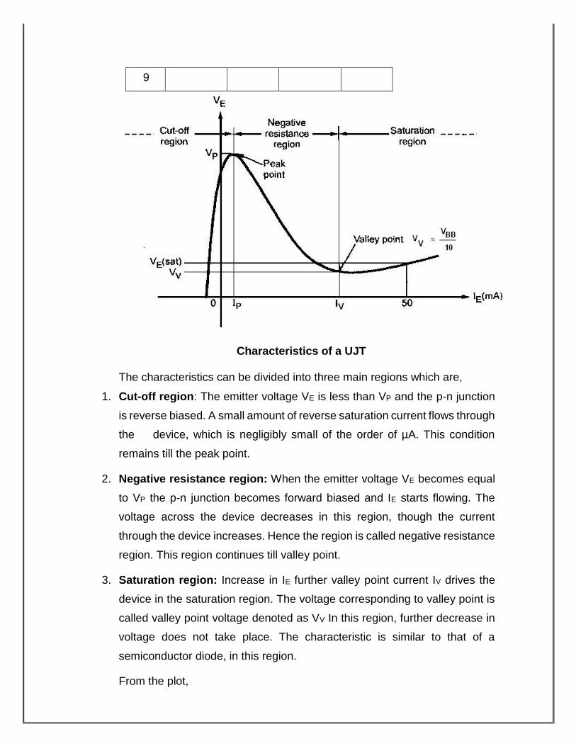
Characteristics of a UJT
The characteristics can be divided into three main regions which are,
1. Cut-off region: The emitter voltage VE is less than VP and the p-n junction
is reverse biased. A small amount of reverse saturation current flows through
the device, which is negligibly small of the order of µA. This condition
remains till the peak point.
2. Negative resistance region: When the emitter voltage VE becomes equal
to VP the p-n junction becomes forward biased and IE starts flowing. The
voltage across the device decreases in this region, though the current
through the device increases. Hence the region is called negative resistance
region. This region continues till valley point.
3. Saturation region: Increase in IE further valley point current IV drives the
device in the saturation region. The voltage corresponding to valley point is
called valley point voltage denoted as VV In this region, further decrease in
voltage does not take place. The characteristic is similar to that of a
semiconductor diode, in this region.
From the plot,
9

(i) VP =
(ii) VV =
(iii) IV =
(iv) η = (VP – VD) / VBB =
Where VD = The diode drop
= 0.3 to 0.7 V
RESULT:
Thus the characteristic of a Uni Junction Transistor(UJT) is analyzed and the peak
voltage (VP), valley point voltage (VV), valley point current (IV) and intrinsic standoff
ratio (η) are determined.

CHARACTERISTICS OF JFET
EX. NO: 11(a) AIM:
To plot the drain and transfer characteristics of a Junction Field Effect Transistor
(JFET) and to calculate the transconductance (gm), drain to source resistance (rd),
amplification factor (µ).
APPARATUS REQUIRED:
S.NO APPARATUS RANGE QUANTITY
1 RPS (0-30)V 2
2 Resistor 220Ω 2
3 DC Voltmeter (0-10)V 1
4 DC Voltmeter (0-30)V 1
5 DC Ammeter (0-30)mA 1
6 JFET BFW11 1
7 Bread board - 1
8 Connecting wires - Few
THEORY:
N-channel JFET Pin Diagram
. The flow of electric charge through a JFET is controlled by constricting the
current-carrying channel. The current depends also on the electric field between
source and drain.
The JFET is a long channel of semiconductor material, doped to contain
abundance of positive charge carriers (p-type), or of negative carriers (n-type)
Contacts at each end form the source and drain. The gate (control) terminal has
doping opposite to that of the channel, which it surrounds, so that there is a P-N
junction at the interface. Terminals to connect with the outside are usually made
Ohmic .

Circuit Diagram for JFET
DRAIN CHARACTERICTICS:
PROCEDURE:
1. Connections are given as per the circuit diagram.
2. The supply is switched ON.
3. The gate-source voltage VGS is kept constant.
4. By varying the drain-source voltage VDS, the various drain current ID is noted.
5. The same procedure is repeated for various gate-source voltage
VGS.
In the Ohmic region, the drain-source voltage is small and the channel
behaves like a fairly ordinary conductor. In this region the current varies roughly in
proportion to the drain-source voltage as if the JFET obeys Ohm's law. However,
as we increase the drain-source voltage and move into the region with a light
background we increase the drain-channel voltage so much that we start to
‘squeeze down’ the channel.
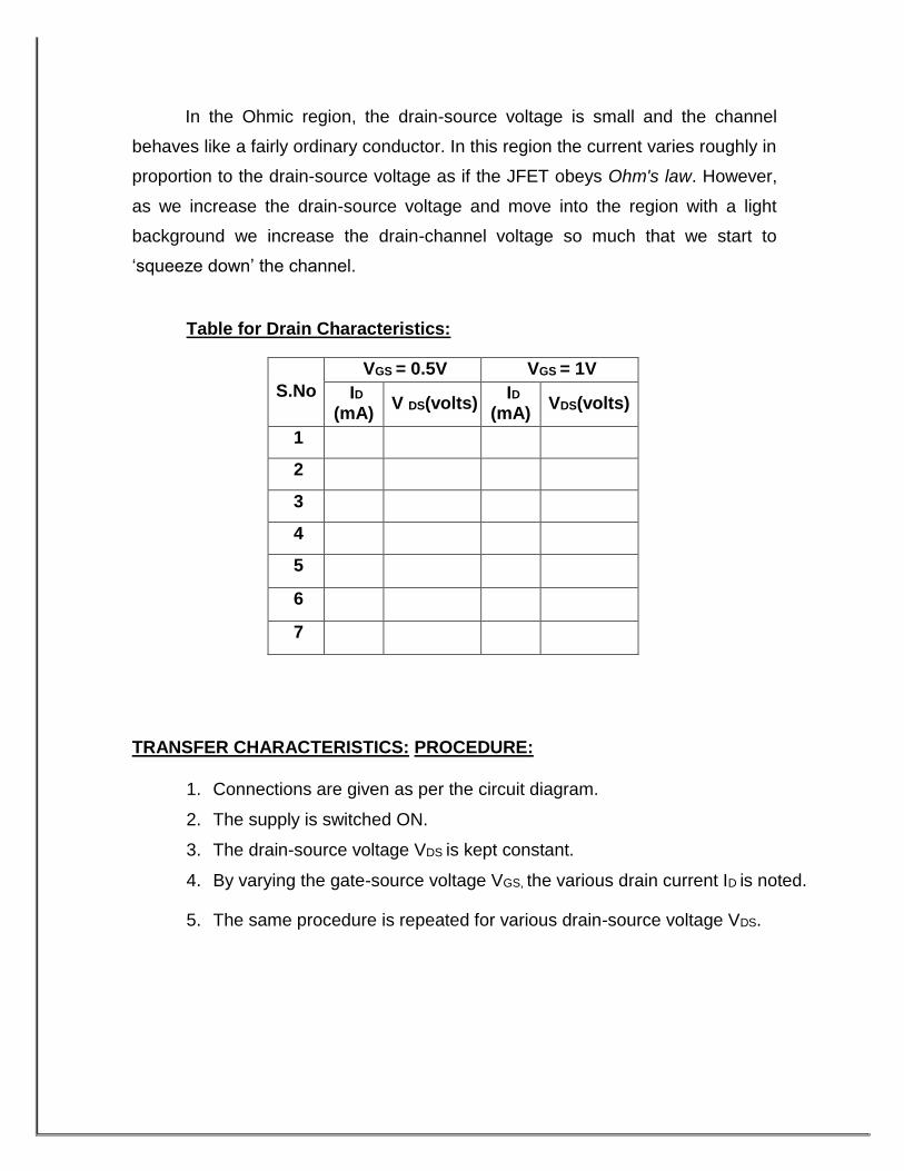
Table for Drain Characteristics:
S.No
VGS = 0.5V VGS = 1V
ID (mA)
V DS(volts) ID
(mA) VDS(volts)
1
2
3
4
5
6
7
TRANSFER CHARACTERISTICS: PROCEDURE:
1. Connections are given as per the circuit diagram.
2. The supply is switched ON.
3. The drain-source voltage VDS is kept constant.
4. By varying the gate-source voltage VGS, the various drain current ID is noted.
5. The same procedure is repeated for various drain-source voltage VDS.
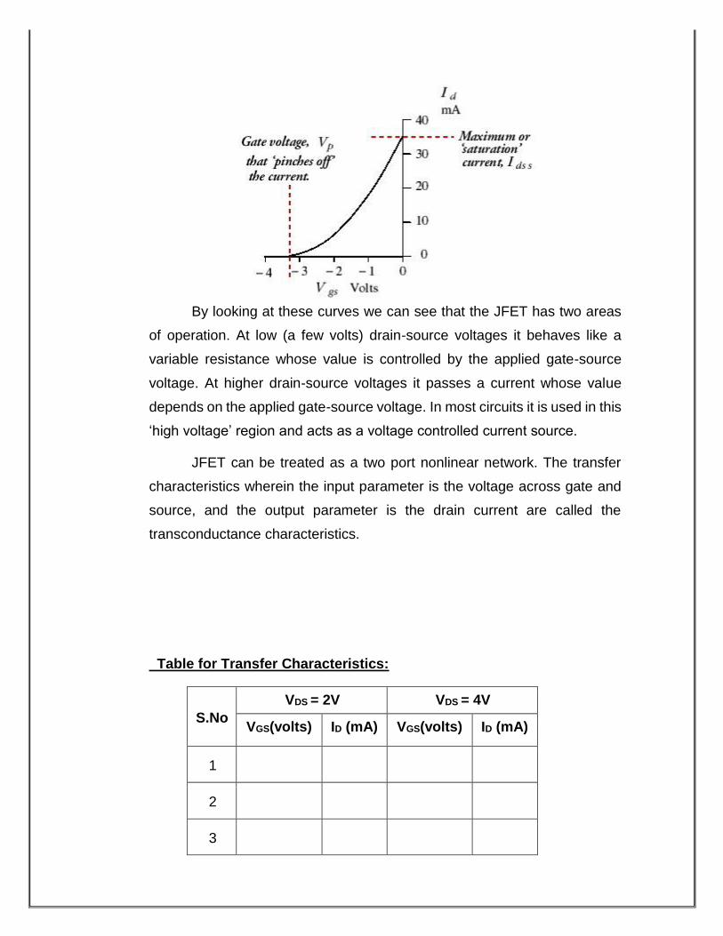
By looking at these curves we can see that the JFET has two areas
of operation. At low (a few volts) drain-source voltages it behaves like a
variable resistance whose value is controlled by the applied gate-source
voltage. At higher drain-source voltages it passes a current whose value
depends on the applied gate-source voltage. In most circuits it is used in this
‘high voltage’ region and acts as a voltage controlled current source.
JFET can be treated as a two port nonlinear network. The transfer
characteristics wherein the input parameter is the voltage across gate and
source, and the output parameter is the drain current are called the
transconductance characteristics.
Table for Transfer Characteristics:
S.No
VDS = 2V VDS = 4V
VGS(volts) ID (mA) VGS(volts) ID (mA)
1
2
3
4
5
6
7
RESULT:
Thus the drain and transfer characteristics of a junction field effect transistor is
analyzed and the transconductance (gm), drain to source resistance (rd),
amplification factor (µ) are calculated.
The transconductance is,
The drain to source resistance is,
The Amplification factor is,
=

CHARACTERISTICS OF MOSFET
EX. NO : 11(b) AIM:
To plot the drain and transfer characteristics of a n-channel depletion type Metal Oxide
Semiconductor Junction Field Effect Transistor (MOSFET).
APPARATUS REQUIRED:
S.NO APPARATUS RANGE QUANTITY
1 RPS (0-30)V 2
2 Resistor 220Ω 2
3 DC Voltmeter (0-10)V 1
4 DC Voltmeter (0-30)V 1
5 DC Ammeter (0-30)mA 1
6 MOSFET 1
7 Bread board - 1
8 Connecting wires - Few
THEORY:
N-channel JFET
The metal–oxide–semiconductor field-effect transistor (MOSFET, MOSFET,
or MOS FET) is a device used to amplify or switch electronic signals. The MOSFET differs from JFET in that it has no p-n junction structure.
Instead, the gate of the MOSFET insulated from the channel by a silicon dioxide (SiO2) layer. Due to this the input resistance of MOSFET is greater than JFET.

Circuit Diagram for MOSFET
DRAIN CHARACTERICTICS: PROCEDURE:
1. Connections are given as per the circuit diagram.
2. The supply is switched ON.
3. The gate-source voltage VGS is kept constant.
4. By varying the drain-source voltage VDS, the various drain current ID is noted.
5. The same procedure is repeated for various gate-source voltage
VGS.
In the Ohmic region, the drain-source voltage is small and the channel
behaves like a fairly ordinary conductor. In this region the current varies roughly in

proportion to the drain-source voltage as if the MOSJFET obeys Ohm's law.
However, as we increase the drain-source voltage and move into the region with a
light background we increase the drain-channel voltage so much that we start to
‘squeeze down’ the channel. It is similar to that of JFET only the difference is that
it has positive part VGS.
Table for Drain Characteristics:
S.No
VGS = VGS =
ID (mA)
V DS(volts) ID
(mA) VDS(volts)
1
2
3
4
5
6
7
TRANSFER CHARACTERISTICS: PROCEDURE:
1. Connections are given as per the circuit diagram.
2. The supply is switched ON.
3. The drain-source voltage VDS is kept constant.
4. By varying the gate-source voltage VGS, the various drain current
ID is noted.
5. The same procedure is repeated for various drain-source voltage VDS.

For positive values of VGS the positive gate will draw additional electrons
from the p-type substrate due to reverse leakage current and establish new carries
through the collisions between accelerating particles. Because of this, as gate to
source voltage increases in positive direction, the drain current also increases.
Table for Transfer Characteristics:
S.No
VDS = VDS =
VGS(volts) ID (mA) VGS(volts) ID (mA)
1
2
3
4
5
6
7
RESULT:
Thus the drain and transfer characteristics of a metal oxide semiconductor
junction field effect transi

CHARACTERISTICS OF DIAC
EX. NO: 11(a)
AIM:
To plot the V-I characteristics of a DIAC. APPARATUS REQUIRED:
S.NO APPARATUS TYPE QUANTITY
1 RPS (0-30)V 1
2 Resistor 1KΩ 1
3 DC Voltmeter (0-30)V 1
5 DC Ammeter (0-30)mA 1
6 DIAC 1
7 Bread board - 1
8 Connecting wires - Few
THEORY:
Construction Symbol The
DIAC is basically two parallel diodes turned in opposite direction having a pair of
four layer diodes for alternating current. It is a bidirectional trigger diode that
conducts current only after its breakdown voltage has been exceeded momentarily.
When this occurs, the resistance of the diode abruptly decreases, leading to a
sharp decrease in the voltage drop across the diode and, usually, a sharp increase
in current flow through the diode. The diode remains "in conduction" until the
current flow through it drops below a value characteristic for the device, called the
holding current. Below this value, the diode switches back to its high-resistance
(non-conducting) state. When used in AC applications this automatically happens
when the current reverses polarity.

FORWARD BIAS:
PROCEDURE:
1. Connections are given as per the circuit diagram.
2. The supply is switched ON.
3. Vary the power supply in regular step and note down the voltage and
current of DIAC.
4. Plot the graph between the voltage and current.
REVERSE BIAS:

PROCEDURE:
1. Connections are given as per the circuit diagram.
2. The supply is switched ON.
3. Vary the power supply in regular step and note down the voltage and current of
DIAC.
4. Plot the graph between the voltage and current.
Table:
S.No FORWARD BIAS REVERSE BIAS
Voltage(V) Current(mA) Voltage(V) Current(mA)
1
2
3
4
5
6
7
8
9
10

V-I characteristics of a DIAC
RESULT:
Thus the V-I characteristics of a DIAC is analyzed.

CHARACTERISTICS OF TRIAC
EX. NO : 11(b) AIM:
To plot the V-I characteristics of a TRIAC.
APPARATUS REQUIRED:
S.NO APPARATUS TYPE QUANTITY
1 RPS (0-30)V 2
2 Resistor 10 KΩ
5 KΩ
1
1
3 DC Voltmeter (0-30)V 1
5 DC Ammeter (0-100)mA 2
6 TRIAC BT136 1
7 Bread board - 1
8 Connecting wires - Few
THEORY:

Pin Diagram
It is basically two SCR’s turned in opposite directions, with a common gate
terminal. It is a bidirectional device. The two main electrodes are called MT1 and
MT2 while common control terminal is called gate G. S The gate terminal is near to
MT1. The triac can be turned ON by applying either positive or negative voltage to
the gate G with respect to the main terminal MT1.
FORWARD BIAS:

PROCEDURE:
1. Connections are given as per the circuit diagram.
2. The supply is switched ON.
3. The Gate current IG is set to 2mA by varying the RPS which connected to the
gate.
4. Vary another power supply which is connected across the terminals of TRIAC
in regular step and note down the voltage and current of TRIAC.
5. Plot the graph between the voltage and current.
REVERSE BIAS:
PROCEDURE:

1. Connections are given as per the circuit diagram.
2. The supply is switched ON.
3. The Gate current IG is set to 2mA by varying the RPS which connected to the
gate.
4. Vary another power supply which is connected across the terminals of TRIAC
in regular step and note down the voltage and current of TRIAC.
5. Plot the graph between the voltage and current.
Table:
S.No
FORWARD BIAS REVERSE BIAS
Gate Current (IG= 2mA) Gate Current (IG= 2mA)
Voltage(V) Current(mA) Voltage(V) Current(mA)
1
2
3
4
5
6
7
8
9
10
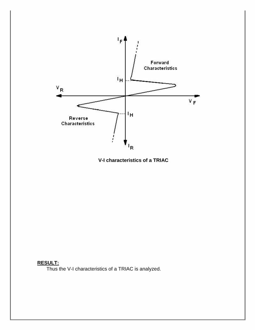
V-I characteristics of a TRIAC
RESULT:
Thus the V-I characteristics of a TRIAC is analyzed.

CHARACTERISTICS OF PHOTO DIODE
EX. NO: 12(a)
AIM:
To plot the characteristics of a Photo Diode. APPARATUS REQUIRED:
S.NO APPARATUS TYPE QUANTITY
1 RPS (0-30)V 1
2 Resistor 1KΩ 1
3 DC Voltmeter (0-30)V 1
4 DC Ammeter (0-50)mA 1
5 Photo Diode 1
6 Bread board - 1
7 Connecting wires - Few
THEORY:
Symbol The photodiode is a semiconductor p-n junction device whose region of operation is
limited to the reverse biased region.
The reverse current without light in diode is in the range of µA. The change
in this current due to the light is also in the range of µA. Thus such a change can
be significantly observed in the reverse current. If the photodiode is forward biased,
the current flowing through it is in mA. The applied forward biased voltage takes the
control of the current instead of the light. The change in forward current due to light
is negligible and cannot be noticed. The resistance of forward biased diode is not
affected by the light. Hence to have significant effect of light on the current and to
operate photodiode as a variable resistance device, it is always connected in
reverse biased condition.
The depletion region width is large. Under normal condition, it carries small
reverse current due to minority charge carriers. When light is incident through glass

window on the p-n junction, photons in the light bombarding the pn junction and
some energy is imparted to the valence electrons. Due to this, valence electrons
are dislodged from the covalent bonds and become free electrons. Thus more
electron-hole pairs are generated. Thus total number of minority charge carriers
increases and hence the reverse current increases.
When there is no light, the reverse biased photodiode carries a current which
is very small and called dark current. It is purely due to thermally generated
minority carriers. When light is allowed to fall on a p-n junction through a small
window, photons transfer energy to valence electrons to make them free. Hence
reverse current increases. It is proportional to the light intensity. The reverse current
is not dependent on reverse voltage and totally depends on light intensity.
PROCEDURE:
1. Connections are given as per the circuit diagram.
2. Connect the patch card from one of the devices mounted in the moving plot
to the main unit.
3. Connect the unit to the 220V supply. Switch ON the toggle switch. LED will
glow that indicating that the unit is ready for operation.
4. Connect the mains card of the light source to 220V AC supply and switch
ON the controller.
5. Adjust the distance between the light source and photo diode. Note down
the current and voltage for various distances.
6. Plot the graph between the reverse voltage and reverse current.
Table:
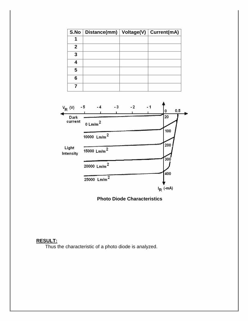
S.No Distance(mm) Voltage(V) Current(mA)
1
2
3
4
5
6
7
Photo Diode Characteristics
RESULT:
Thus the characteristic of a photo diode is analyzed.

CHARACTERISTICS OF PHOTO TRANSISTOR
EX. NO: 12(b) AIM:
To plot the characteristics of a photo transistor.
APPARATUS REQUIRED:
S.NO APPARATUS TYPE QUANTITY
1 RPS (0-30)V 1
2 Resistor 1KΩ 1
3 DC Voltmeter (0-30)V 1
4 DC Ammeter (0-50)mA 1
5 Photo Transistor 1
6 Bread board - 1
7 Connecting wires - Few
THEORY:
The phototransistor has a light sensitive collector to base junction. A lens is
used in a transistor package to expose base to an incident light. When no light is
incident, a small leakage current flow from collector to emitter due to small thermal
generation. This is very small current, of the order of nA. This is called a dark
Construction Symbol
C
E

current. When the base is exposed to the light, the base current is produced which
is proportional to the light intensity.
PROCEDURE:
1. Connections are given as per the circuit diagram.
2. Connect the patch card from one of the devices mounted in the moving plot
to the main unit.
3. Connect the unit to the 220V supply. Switch ON the toggle switch. LED will
glow that indicating that the unit is ready for operation.
4. Connect the mains card of the light source to 220V AC supply and switch
ON the controller.
5. Adjust the distance between the light source and photo transistor. Note down
the collector current (IC) and voltage between collector and emitter (VCE) for
various distances.
6. Plot the graph between the collector current (IC) and voltage between
collector and emitter (VCE).

Table:
S.No Distance(mm) VCE(V) IC(mA)
1
2
3
4
5
6
7
Photo Transistor Characteristics
RESULT:
Thus the characteristics of a photo transistor are analyzed.

28
12. TRANSIENT RESPONSE OF RC AND RL CIRCUITS FOR DC INPUT’S.
AIM:
To construct RL & RC transient circuit and to draw the transient curves.
APPARATUS REQUIRED:
THEORY:
Electrical devices
are controlled by
switches which are
closed to connect
supply to the
device, or opened
in order to disconnect the supply to the device. The switching operation will change the current and voltage in
the device. The purely resistive devices will allow instantaneous change in current and voltage. An
inductive device will not allow sudden change in current and capacitance device will not allow sudden change
in voltage. Hence when switching operation is performed in inductive and capacitive devices, the current &
voltage in device will take a certain time to change from pre switching value to steady state value after switching.
This phenomenon is known as transient. The study of switching condition in the circuit is called transient
analysis.The state of the circuit from instant of switching to attainment of steady state is called transient state.
The time duration from the instant of switching till the steady state is called transient period. The current &
voltage of circuit elements during transient period is called transient response.
FORMULA:
Time constant of RC circuit = RC
PROCEDURE:
S.NO. NAME OF
THE
EQUIPMENT
RANGE TYPE QTY.
1. RPS (0-30)V DC 1
2. Ammeter (0-10)mA MC 1
3. Voltmeter (0-10)V MC 1
4. Resistor 10 KΩ
- 3
5. Capacitor 1000 µ F - 1
6. Bread board - - 1
7. Connecting
wires
- Single strand As required
29
• Connections are made as per the circuit diagram.
• Before switching ON the power supply the switch S should be in off position • Now switch
ON the power supply and change the switch to ON position.
• The voltage is gradually increased and note down the reading of ammeter and voltmeter for
each time duration in RC.In RL circuit measure the Ammeter reading. • Tabulate the
readings and draw the graph of Vc(t)Vs t
CIRCUIT DIAGRAM:
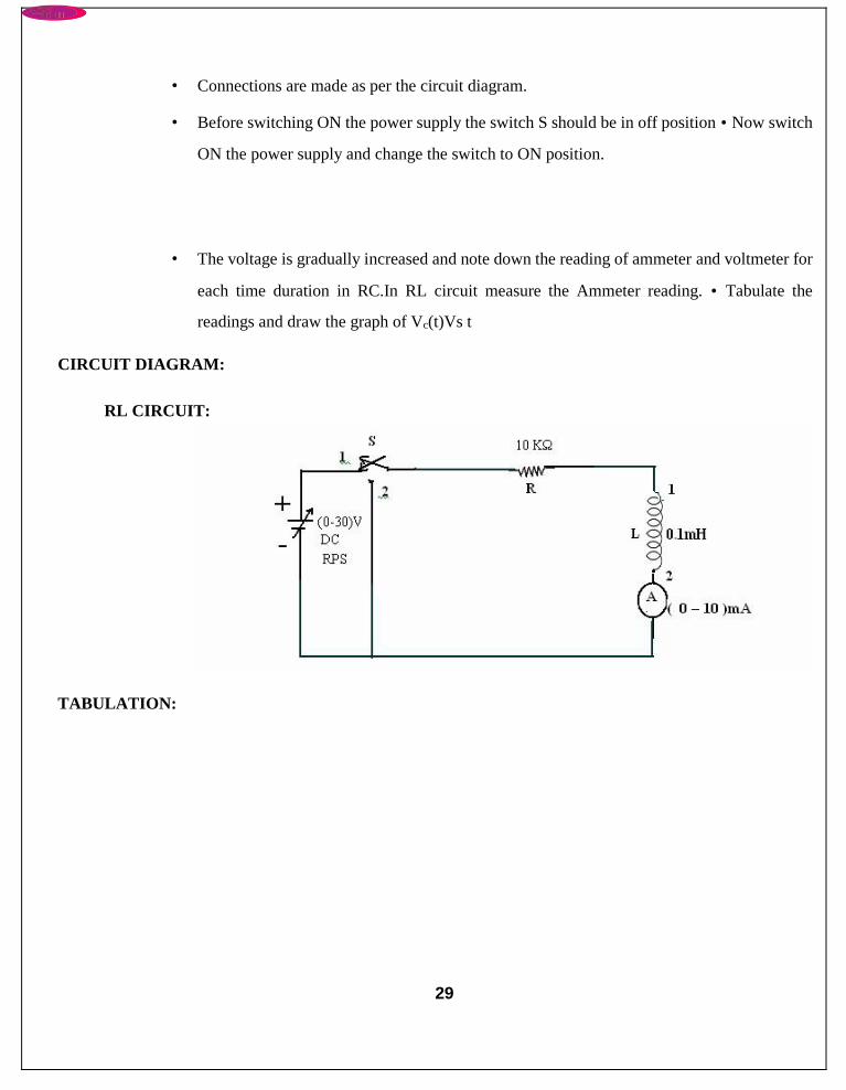
RL CIRCUIT:
TABULATION:
30
MODEL CALCULATION &
ANALYSIS:
MODEL GRAPH:
CIRCUIT DIAGRAM:
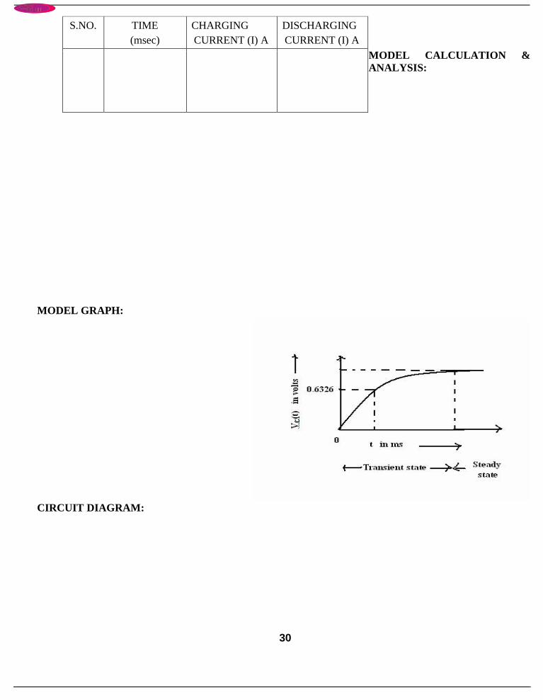
S.NO. TIME
(msec)
CHARGING
CURRENT (I) A
DISCHARGING
CURRENT (I) A
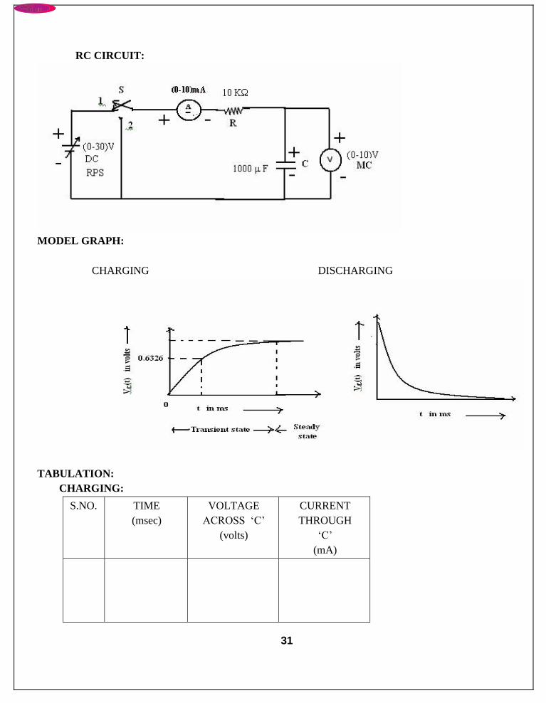
31
RC CIRCUIT:
MODEL GRAPH:
CHARGING DISCHARGING
TABULATION:
CHARGING:
S.NO. TIME
(msec)
VOLTAGE
ACROSS ‘C’
(volts)
CURRENT
THROUGH
‘C’
(mA)

32
MODEL CALCULATION & ANALYSI
TABULATION:
DISCHARGING:
S.NO. TIME
(msec)
VOLTAGE
ACROSS ‘C’
(volts)
CURRENT
THROUGH
‘C’
(mA)
MODEL CALCULATION & ANALYSIS:
RESULT:
Thus the transient response of RL & RC circuit for DC input was verified.
91
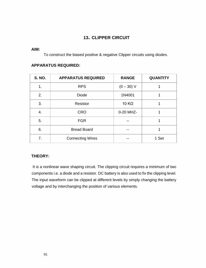
13. CLIPPER CIRCUIT
AIM:
To construct the biased positive & negative Clipper circuits using diodes.
APPARATUS REQUIRED:
S. NO. APPARATUS REQUIRED RANGE QUANTITY
1. RPS (0 – 30) V 1
2. Diode 1N4001 1
3. Resistor 10 KΩ 1
4. CRO 0-20 MHZ- 1
5. FGR -- 1
6. Bread Board -- 1
7. Connecting Wires -- 1 Set
THEORY:
It is a nonlinear wave shaping circuit. The clipping circuit requires a minimum of two
components i.e. a diode and a resistor. DC battery is also used to fix the clipping level.
The input waveform can be clipped at different levels by simply changing the battery
voltage and by interchanging the position of various elements.
92
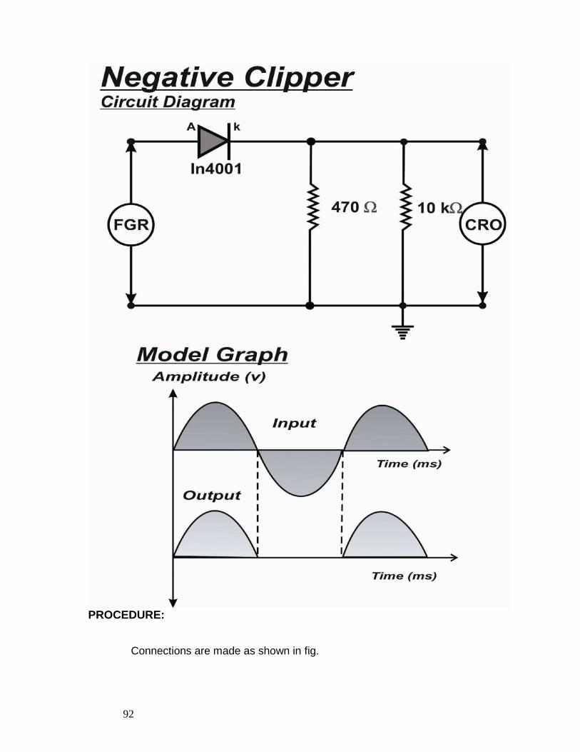
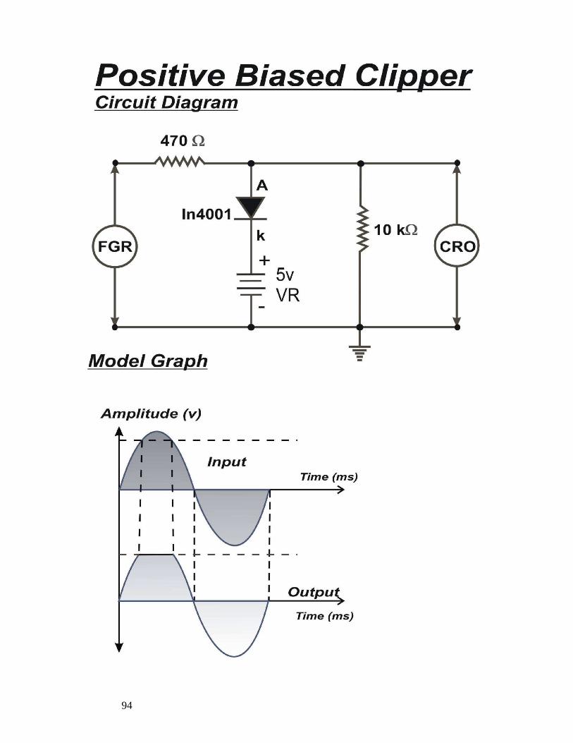
PROCEDURE:
Connections are made as shown in fig.

93
Power supply is switched ON.
Using Function Generator we can vary the frequency and fixed at particular
frequency.
Now the corresponding input and output waveforms are drawn.
Amplitude and time, input & output waveforms are drawn.
And graph is drawn for input and output waveform. Power supply is switched OFF.
94

95
APPLICATION:
It is used in radar applications.
Used in digital computers
Widely used in radio and television receivers
VIVA QUESTIONS:
What is clipper?
What is meant by biased clipper?
Mention the application of clipper?
Differentiate between series and shunt positive clipper?

96
NEGATIVE BIASED CLIPPER
MODEL GRAPH
Circuit Diagram
K 10 Ω
- 5 VR
K A
FGR CRO
IN 4001
-
+

97
RESULT:
Thus the Positive and Negative Clipper Circuits were studied and constructed and its input and output waveforms were drawn.
* * * * * * * * * *
98
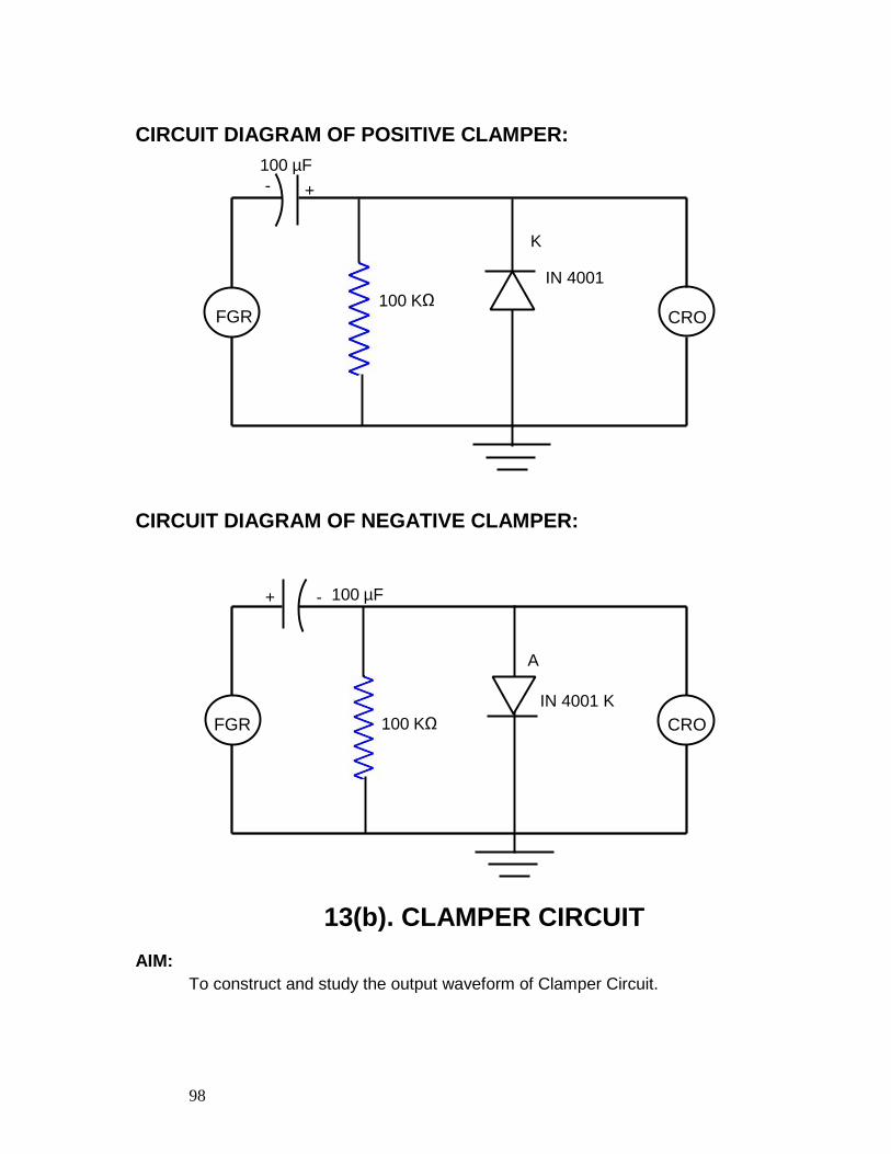
CIRCUIT DIAGRAM OF POSITIVE CLAMPER:
CIRCUIT DIAGRAM OF NEGATIVE CLAMPER:
13(b). CLAMPER CIRCUIT
AIM:
To construct and study the output waveform of Clamper Circuit.
100 µF
FGR CRO 100 K Ω
K
IN 4001
- +
- +
K 100 Ω
100 µF
IN 4001 K
A
FGR CRO

99
APPARATUS REQUIRED:
S. NO. APPARATUS REQUIRED RANGE QUANTITY
1. Diode 1N4001 1
2. Capacitor 100µF/25V 1
3. CRO 0- 20 MHZ 1
4. FGR -- 1
5. Bread Board -- 1
6. Connecting Wires -- 15
THEORY:
Clamping is the process of introducing a dc level into an ac signal. Clampers are also sometimes known as dc restorers.
Clamping is the process of shifting the input signal above or below the zero level.
A clamping circuit should not change peak to peak value of the signal; it should only change the DC level. To do so, a clamping circuit uses a capacitor together with a diode and a resistor.
PROCEDURE:
Connections are made as shown in fig.
Switched ON the Function generator
Now corresponding input and output waveforms are visible at the monitor of
CRO.
Amplitude and Time of input and output waveform is measured and tabulated.
MODEL GRAPH
POSITIVE CLAMPER
Amplitude (v)

100
2Vm
Vm
Time (ms)
NEGATIVE CLAMPER
Amplitude (v)
Time (ms)
Time (ms)
Time (ms)
- Vm
-2 Vm