Embed Size (px)
Citation preview
SEMBODAI RUKMANI VARATHARAJAN ENGINEERING COLLEGE
SEMBODAI, VEDARANIAM [T.K],
NAGAPATTINAM [Dist] -614820.
DEPARTMENT OF ELECTRONICS AND COMMUNICATION ENGINEERING
LAB MANUAL
NAME
REG.No
BRANCH
YEAR SEMESTER
EC2405 – OPTICAL AND MICROWAVE LAB
SEMBODAI RUKMANI VARATHARAJAN ENGINEERING COLLEGE
SEMBODAI, VEDARANIAM [T.K],
NAGAPATTINAM [Dist] -614820.
DEPARTMENT OF ELECTRONICS AND COMMUNICATION ENGINEERING
ACADEMIC YEAR 2015-2016 ODD SEM
EC2405 – OPTICAL AND MICROWAVE LAB
IV YEAR / VII SEMESTER
Prepared By
Mr.G.SUNDAR M.Tech,MISTE.,
AP/ECE
SETTING UP FIBER OPTIC ANALOG LINK
Ex. No: 01
Date :
1.1 OBJECTIVE: The objective of this experiment is to study an 660 nm/ 950 nm Fiber Optic Analog Link. In this experiment you will study the relationship between the input signal & received signal. 1.2 APPARATUS REQUIRED:
1.3 THEORY: Fiber Optic Links can be used for transmission of digital as well as analog signals. Basically a fiber optic link contains three main elements, a transmitter, an optical fiber and a receiver. The transmitter module takes the input signal in electrical form and then transforms it into optical (light) energy containing the same information. The optical fiber is the medium which carries this energy to the receiver. At the receiver, light is converted back into electrical form with the same pattern as originally fed to the transmitter. TRANSMITTER: Fiber optic transmitters are typically composed of a buffer, driver and optical source. The buffer electronics provides both an electrical connection and isolation between the transmitter and the electrical system supplying the data. The driver electronics provides electrical power to the optical source in a fashion that duplicates the pattern of data being fed to the transmitter. Finally the optical source (LED) converts the electrical current to light energy with the same pattern. RECEIVER: The function of the receiver is to convert the optical energy into electrical form which is then conditioned to reproduce the transmitted electrical signal in its original form. The detector SFH250V used in the kit has a diode type output. The parameters usually considered in the case of detector are it's responsivity at peak wavelength and response time. SFH250V has responsivity of about 4 mA per 10 mW of incident optical energy at 950 nm and it has rise and fall time of 0.01 m sec. PIN photodiode is normally reverse biased.
S.No Name of the Components Specification Quantity
1 Fiber optic trainer kit. Link A 1
2 CRO - 1
3 Power supply (0±12)v 1
4 Fiber optic cable 950 nm 1
5 Connecting Chords. - As required
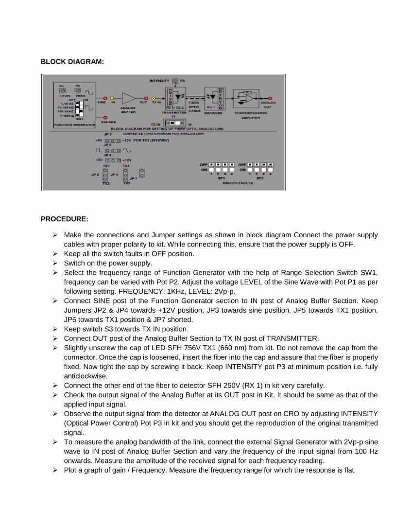
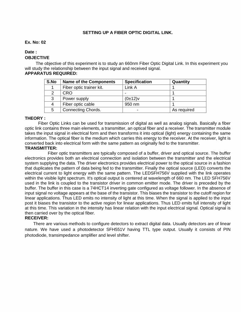
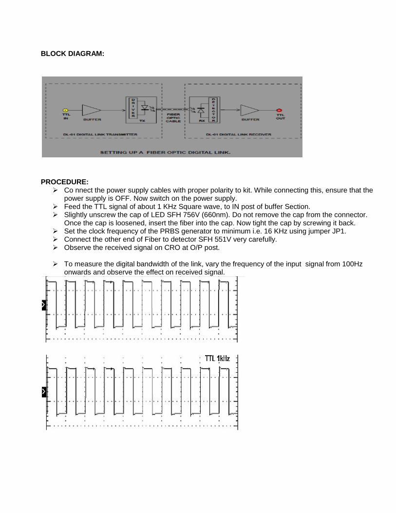
BLOCK DIAGRAM:
PROCEDURE:
Make the connections and Jumper settings as shown in block diagram Connect the power supply
cables with proper polarity to kit. While connecting this, ensure that the power supply is OFF.
Keep all the switch faults in OFF position.
Switch on the power supply.
Select the frequency range of Function Generator with the help of Range Selection Switch SW1,
frequency can be varied with Pot P2. Adjust the voltage LEVEL of the Sine Wave with Pot P1 as per
following setting. FREQUENCY: 1KHz, LEVEL: 2Vp-p.
Connect SINE post of the Function Generator section to IN post of Analog Buffer Section. Keep
Jumpers JP2 & JP4 towards +12V position, JP3 towards sine position, JP5 towards TX1 position,
JP6 towards TX1 position & JP7 shorted.
Keep switch S3 towards TX IN position.
Connect OUT post of the Analog Buffer Section to TX IN post of TRANSMITTER.
Slightly unscrew the cap of LED SFH 756V TX1 (660 nm) from kit. Do not remove the cap from the
connector. Once the cap is loosened, insert the fiber into the cap and assure that the fiber is properly
fixed. Now tight the cap by screwing it back. Keep INTENSITY pot P3 at minimum position i.e. fully
anticlockwise.
Connect the other end of the fiber to detector SFH 250V (RX 1) in kit very carefully.
Check the output signal of the Analog Buffer at its OUT post in Kit. It should be same as that of the
applied input signal.
Observe the output signal from the detector at ANALOG OUT post on CRO by adjusting INTENSITY
(Optical Power Control) Pot P3 in kit and you should get the reproduction of the original transmitted
signal.
To measure the analog bandwidth of the link, connect the external Signal Generator with 2Vp-p sine
wave to IN post of Analog Buffer Section and vary the frequency of the input signal from 100 Hz
onwards. Measure the amplitude of the received signal for each frequency reading.
Plot a graph of gain / Frequency. Measure the frequency range for which the response is flat.
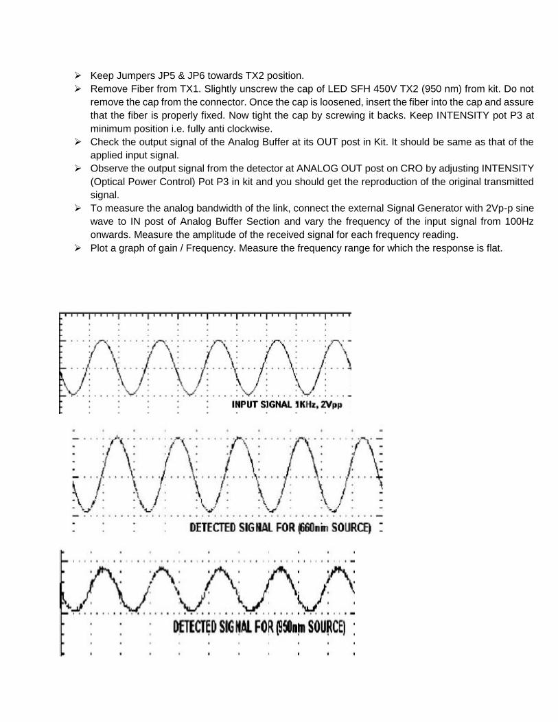
Keep Jumpers JP5 & JP6 towards TX2 position.
Remove Fiber from TX1. Slightly unscrew the cap of LED SFH 450V TX2 (950 nm) from kit. Do not
remove the cap from the connector. Once the cap is loosened, insert the fiber into the cap and assure
that the fiber is properly fixed. Now tight the cap by screwing it backs. Keep INTENSITY pot P3 at
minimum position i.e. fully anti clockwise.
Check the output signal of the Analog Buffer at its OUT post in Kit. It should be same as that of the
applied input signal.
Observe the output signal from the detector at ANALOG OUT post on CRO by adjusting INTENSITY
(Optical Power Control) Pot P3 in kit and you should get the reproduction of the original transmitted
signal.
To measure the analog bandwidth of the link, connect the external Signal Generator with 2Vp-p sine
wave to IN post of Analog Buffer Section and vary the frequency of the input signal from 100Hz
onwards. Measure the amplitude of the received signal for each frequency reading.
Plot a graph of gain / Frequency. Measure the frequency range for which the response is flat.

1.5 TABULATION:
Signal Amplitude(V) Time(ms) Frequency(Hz)
1.6 RESULT: Thus the relationship between input and output waves was obtained.
SETTING UP A FIBER OPTIC DIGITAL LINK.
Ex. No: 02
Date :
OBJECTIVE
The objective of this experiment is to study an 660nm Fiber Optic Digital Link. In this experiment you will study the relationship between the input signal and received signal. APPARATUS REQUIRED: THEORY : Fiber Optic Links can be used for transmission of digital as well as analog signals. Basically a fiber optic link contains three main elements, a transmitter, an optical fiber and a receiver. The transmitter module takes the input signal in electrical form and then transforms it into optical (light) energy containing the same information. The optical fiber is the medium which carries this energy to the receiver. At the receiver, light is converted back into electrical form with the same pattern as originally fed to the transmitter. TRANSMITTER: Fiber optic transmitters are typically composed of a buffer, driver and optical source. The buffer electronics provides both an electrical connection and isolation between the transmitter and the electrical system supplying the data. The driver electronics provides electrical power to the optical source in a fashion that duplicates the pattern of data being fed to the transmitter. Finally the optical source (LED) converts the electrical current to light energy with the same pattern. The LEDSFH756V supplied with the link operates within the visible light spectrum. It's optical output is centered at wavelength of 660 nm. The LED SFH756V used in the link is coupled to the transistor driver in common emitter mode. The driver is preceded by the buffer. The buffer in this case is a 74HCT14 inverting gate configured as voltage follower. In the absence of input signal no voltage appears at the base of the transistor. This biases the transistor to the cutoff region for linear applications. Thus LED emits no intensity of light at this time. When the signal is applied to the input post it biases the transistor to the active region for linear applications. Thus LED emits full intensity of light at this time. This variation in the intensity has linear relation with the input electrical signal. Optical signal is then carried over by the optical fiber. RECEIVER:
There are various methods to configure detectors to extract digital data. Usually detectors are of linear
nature. We have used a photodetector SFH551V having TTL type output. Usually it consists of PIN
photodiode, transimpedance amplifier and level shifter.
S.No Name of the Components Specification Quantity
1 Fiber optic trainer kit. Link A 1
2 CRO - 1
3 Power supply (0±12)v 1
4 Fiber optic cable 950 nm 1
5 Connecting Chords. - As required
BLOCK DIAGRAM:
PROCEDURE: Co nnect the power supply cables with proper polarity to kit. While connecting this, ensure that the
power supply is OFF. Now switch on the power supply. Feed the TTL signal of about 1 KHz Square wave, to IN post of buffer Section. Slightly unscrew the cap of LED SFH 756V (660nm). Do not remove the cap from the connector.
Once the cap is loosened, insert the fiber into the cap. Now tight the cap by screwing it back. Set the clock frequency of the PRBS generator to minimum i.e. 16 KHz using jumper JP1. Connect the other end of Fiber to detector SFH 551V very carefully. Observe the received signal on CRO at O/P post.
To measure the digital bandwidth of the link, vary the frequency of the input signal from 100Hz
onwards and observe the effect on received signal.
1.5 TABULATION:
Signal Amplitude(V) Time(ms) Frequency(Hz)
RESULT: Thus the relationship between input and output waves was obtained.
STUDY OF NUMERICAL APERTURE OF OPTICAL FIBER.
Ex. No: 03
Date :
OBJECTIVE
The objective of this experiment is to measure the numerical aperture of the plastic
fiber provided with the kit using 660 nm wavelength LED.
EQUIPMENTS:
.
THEORY:
Numerical aperture refers to the maximum angle at which the light incident on the fiber end is totally internally reflected and is transmitted properly along the fiber. The cone formed by the rotation of this angle along the axis of the fiber is the cone acceptance of the fiber. The light ray should strike the fiber end within its cone of acceptance, else it is refracted out of the fiber core. CONSIDERATIONS IN NA MEASUREMENT:
It is very important that the optical source should be properly aligned with the cable and distance from
the launched point and the cable is properly selected to ensure that the maximum amount of optical power
is transferred to the cable.
PROCEDURE:
Connect the power supply cables with proper polarity to kit. While connecting this, ensure that the
power supply is OFF. Do not apply any TTL signal from Function Generator. Make the connections
as shown in block diag.
Keep all the switch faults in OFF position.
Keep Pot P3 fully Clockwise Position and P4 fully anticlockwise position.
Slightly unscrew the cap of LED SFH756V (660 nm). Do not remove the cap from the connector.
Once the cap is loosened, insert the fiber into the cap. Now tight the cap by screwing it back. Keep
Jumpers JP2 towards +5V position, JP3 towards sine position, JP5 & JP6 towards TX1 position.
Keep switch S3 towards VI position.
Insert the other end of the fiber into the numerical aperture measurement jig. Hold the white sheet
facing the fiber. Adjust the fiber such that its cut face is perpendicular to the axis of the fiber.
Keep the distance of about 10 mm between the fiber tip and the screen. Gently tighten the screw and
thus fix the fiber in the place.
Now adjust Pot P4 fully Clockwise Position and observe the illuminated circular patch of light on the
screen.
Measure exactly the distance d and also the vertical and horizontal diameters MR and PN indicated
in the block diagram.
Mean radius is calculated using the following formula. r = (MR + PN) / 4
S.No Name of the Components Specification Quantity
1 Fiber optic trainer kit. Link A 1
2 CRO - 1
3 Power supply (0±12)v 1
4 Fiber optic cable 950 nm 1
5 NA JIG.
6 Connecting Chords. - As required
Find the numerical aperture of the fiber using the formula. NA = sin max = r / d + r Where max is the
maximum angle at which the light incident is properly transmitted through the fiber.
BLOCK DIAGRAM:
TABULATION:
WIDTH IN cm Distance in cm NA Ѳ
RESULT: Thus the numerical aperture of the fiber is calculated.
STUDY OF PROPAGATION LOSSES IN OPTICAL FIBER
Ex. No: 04
Date :
OBJECTIVE
The objective of this experiment is to measure propagation loss in plastic fiber provided with the Lab
for three different wavelengths of radiation as 950 nm, 660 nm.
EQUIPMENTS:
.
THEORY:
Optical fibers are available in different variety of materials. These materials are usually selected by
taking into account their absorption characteristics for different wavelengths of light. In case of optical fiber,
since the signal is transmitted in the form of light which is completely different in nature as that of electrons,
one has to consider the interaction of matter with the radiation to study the losses in fiber. Losses are
introduced in fiber due to various reasons. As light propagates from one end of fiber to another end, part of
it is absorbed in the material exhibiting absorption loss. Also part of the light is reflected back or in some
other directions from the impurity particles present in the material contributing to the loss of the signal at the
other end of the fiber. In general terms it is known as propagation loss. Plastic fibers have higher loss of the
order of 180 dB/Km. Whenever the condition for angle of incidence of the incident light is violated the losses
are introduced due to refraction of light. This occurs when fiber is subjected to bending. Lower the radius of
curvature more is the loss. Another losses are due to the coupling of fiber at LED and photo detector ends.
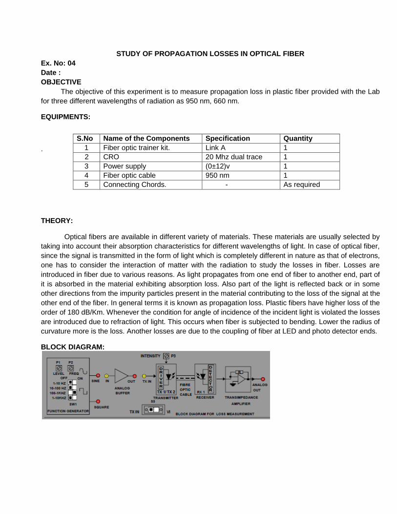
BLOCK DIAGRAM:
S.No Name of the Components Specification Quantity
1 Fiber optic trainer kit. Link A 1
2 CRO 20 Mhz dual trace 1
3 Power supply (0±12)v 1
4 Fiber optic cable 950 nm 1
5 Connecting Chords. - As required
PROCEDURE:
Make the connections and Jumper settings as shown in block diagram Connect the power supply
cables with proper polarity to kit. While connecting this, ensure that the power supply is OFF.
Keep all the switch faults in OFF position.
Switch on the power supply.
Select the frequency range of Function Generator with the help of Range Selection Switch SW1,
frequency can be varied with Pot P2. Adjust the voltage LEVEL of the Sine Wave with Pot P1 as per
following setting. FREQUENCY: 1KHz, LEVEL: 2Vp-p.
Connect SINE post of the Function Generator section to IN post of Analog Buffer Section. Keep
Jumpers JP2 & JP4 towards +12V position, JP3 towards sine position, JP5 towards TX1 position,
JP6 towards TX1 position & JP7 shorted.
Keep switch S3 towards TX IN position.
Connect OUT post of the Analog Buffer Section to TX IN post of TRANSMITTER.
Slightly unscrew the cap of LED SFH 756V TX1 (660 nm) from kit. Do not remove the cap from the
connector. Once the cap is loosened, insert the fiber into the cap and assure that the fiber is properly
fixed. Now tight the cap by screwing it back. Keep INTENSITY pot P3 at minimum position i.e. fully
anticlockwise.
Connect the other end of the fiber to detector SFH 250V (RX 1) in kit very carefully.
Check the output signal of the Analog Buffer at its OUT post in Kit. It should be same as that of the
applied input signal.
Now replace 1 meter fiber by 3 meter fiber without disturbing any of the previous settings. Measure
the amplitude level at the receiver side again. You will notice that it is less than the previous one.
Mark this as V2.
If alpha is the attenuation of the fiber then we have, P1/P2=V1/V2=e [-alpha (L1+L2)] where alpha =
nepers / meter L1 = fiber length for V1 L2 = fiber length for V2 This alpha is for the wavelength of 950
nm. To get the alpha for 660 nm wavelength proceed as follows.
Remove fiber from TX2 & connect it to TX1.
Keep Jumpers JP5 & JP6 towards TX1 position.
Observe the output signal from the detector at ANALOG OUT post on CRO by adjusting INTENSITY
(Optical Power Control) Pot P3 in kit and you should get the reproduction of the original transmitted
signal. Mark this amplitude level as V1.
Now replace 1 meter fiber by 3 meter fiber without disturbing any of the previous settings. Measure
the amplitude level at the receiver side again. You will notice that it is less than the previous one.
Mark this as V2. If alpha is the attenuation of the fiber then we have, P1/P2=V1/V2=e [-alpha (L1+L2)]
where alpha = nepers / meter
L1 = fiber length for V1 L2 = fiber length for V2
Compare the values of alpha and find out the wavelength which has less attenuation in the fiber.
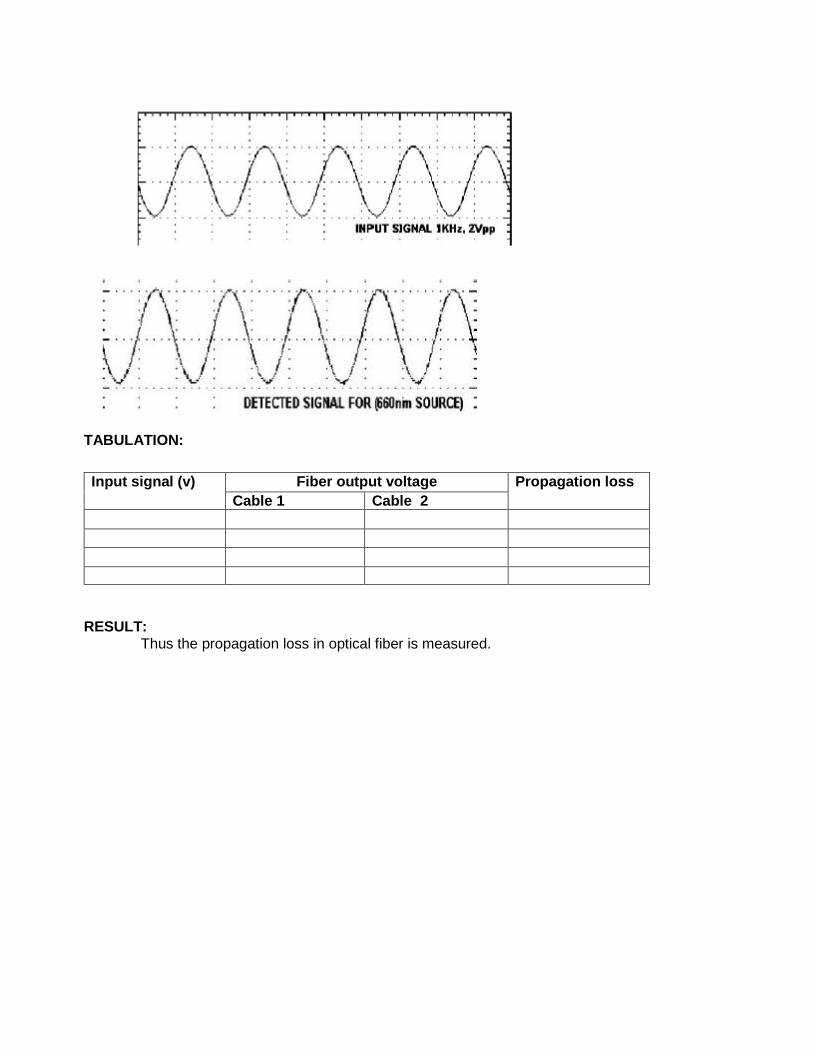
TABULATION:
RESULT: Thus the propagation loss in optical fiber is measured.
Input signal (v) Fiber output voltage Propagation loss
Cable 1 Cable 2
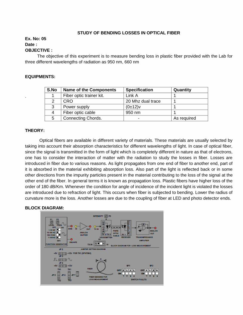
STUDY OF BENDING LOSSES IN OPTICAL FIBER
Ex. No: 05
Date :
OBJECTIVE :
The objective of this experiment is to measure bending loss in plastic fiber provided with the Lab for
three different wavelengths of radiation as 950 nm, 660 nm
EQUIPMENTS:
.
THEORY:
Optical fibers are available in different variety of materials. These materials are usually selected by
taking into account their absorption characteristics for different wavelengths of light. In case of optical fiber,
since the signal is transmitted in the form of light which is completely different in nature as that of electrons,
one has to consider the interaction of matter with the radiation to study the losses in fiber. Losses are
introduced in fiber due to various reasons. As light propagates from one end of fiber to another end, part of
it is absorbed in the material exhibiting absorption loss. Also part of the light is reflected back or in some
other directions from the impurity particles present in the material contributing to the loss of the signal at the
other end of the fiber. In general terms it is known as propagation loss. Plastic fibers have higher loss of the
order of 180 dB/Km. Whenever the condition for angle of incidence of the incident light is violated the losses
are introduced due to refraction of light. This occurs when fiber is subjected to bending. Lower the radius of
curvature more is the loss. Another losses are due to the coupling of fiber at LED and photo detector ends.
BLOCK DIAGRAM:
S.No Name of the Components Specification Quantity
1 Fiber optic trainer kit. Link A 1
2 CRO 20 Mhz dual trace 1
3 Power supply (0±12)v 1
4 Fiber optic cable 950 nm 1
5 Connecting Chords. - As required
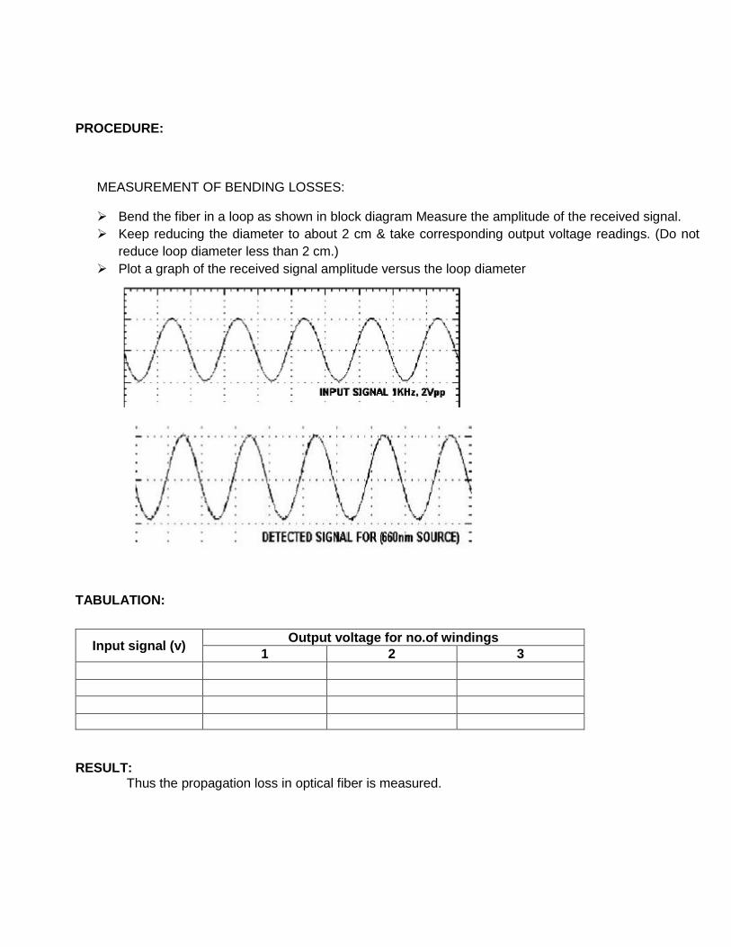
PROCEDURE:
MEASUREMENT OF BENDING LOSSES:
Bend the fiber in a loop as shown in block diagram Measure the amplitude of the received signal.
Keep reducing the diameter to about 2 cm & take corresponding output voltage readings. (Do not
reduce loop diameter less than 2 cm.)
Plot a graph of the received signal amplitude versus the loop diameter
TABULATION:
RESULT: Thus the propagation loss in optical fiber is measured.
Input signal (v) Output voltage for no.of windings
1 2 3
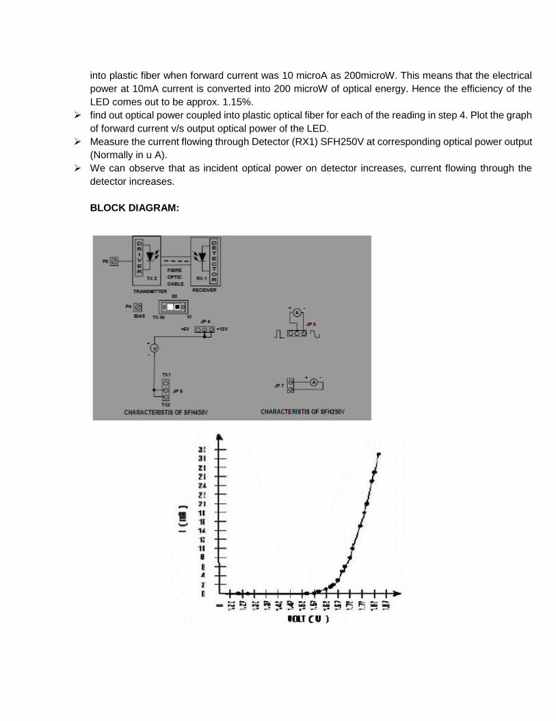
STUDY OF CHARACTERISTICS OF FIBER OPTIC LED AND DETECTOR
Ex. No: 06
Date :
OBJECTIVE :
To study the VI characteristics of fiber optic LED’S.
EQUIPMENTS:
THEORY:
In optical fiber communication system, electrical signal is first converted into optical signal with the
help of E/O conversion device as LED. After this optical signal is transmitted through optical fiber, it is
retrieved in its original electrical form with the help O/E conversion device as photodetector. Different
technologies employed in chip fabrication lead to significant variation in parameters for the various emitter
diodes. All the emitters distinguish themselves in offering high output power coupled into the plastic fiber.
Data sheets for LEDs usually specify electrical and optical characteristics, out of which are important peak
wavelength of emission, conversion efficiency (usually specified in terms of power launched in optical fiber
for specified forward current), optical rise and fall times which put the limitation on operating frequency,
maximum forward current through LED and typical forward voltage across LED. Photodetectors usually
comes in variety of forms like photoconductive, photovoltaic, transistor type output and diode type output.
Here also characteristics to be taken into account are response time of the detector which puts the imitation
on the operating frequency, wavelength sensitivity and responsivity.
PROCEDURE:
Make the jumper and switch settings as shown in the jumper diagram. Keep pot P4 in fully clockwise
position.
Connect the ammeter with the jumper connecting wires (provided along with the kit) in jumpers JP3
as shown in the diagram.
Connect the voltmeter with the jumper wires to JP5 and JP2 at positions as shown in the diagram.
Connect the ammeter with the jumper connecting wires (provided along with the kit) in jumpers JP7
as shown in the diagram.
Switch on the power supply. Keep the potentiometer P3 in its minimum position (fully anticlockwise
position), P4 is used to control biasing voltage of the LED. To get the VI characteristics of LED, rotate
P3 slowly and measure forward current and corresponding forward voltage of the LED, Take number
of such readings for forward voltage, forward current & optical power. Keep SW towards VI position.
Connect 1Meter Fiber between TX1 & RX1.
For each reading taken above, find out the power, which is product of I and V. This is the electrical
power supplied to the LED. Data sheets for the LED specifies optical power coupled
S.No Name of the Components Specification Quantity
1 Fiber optic trainer kit. Link A 1
2 CRO 20 Mhz dual trace 1
3 Power supply (0±12)v 1
4 Fiber optic cable 1,3 meter 950 nm 1
5 Connecting Chords. - As required
into plastic fiber when forward current was 10 microA as 200microW. This means that the electrical
power at 10mA current is converted into 200 microW of optical energy. Hence the efficiency of the
LED comes out to be approx. 1.15%.
find out optical power coupled into plastic optical fiber for each of the reading in step 4. Plot the graph
of forward current v/s output optical power of the LED.
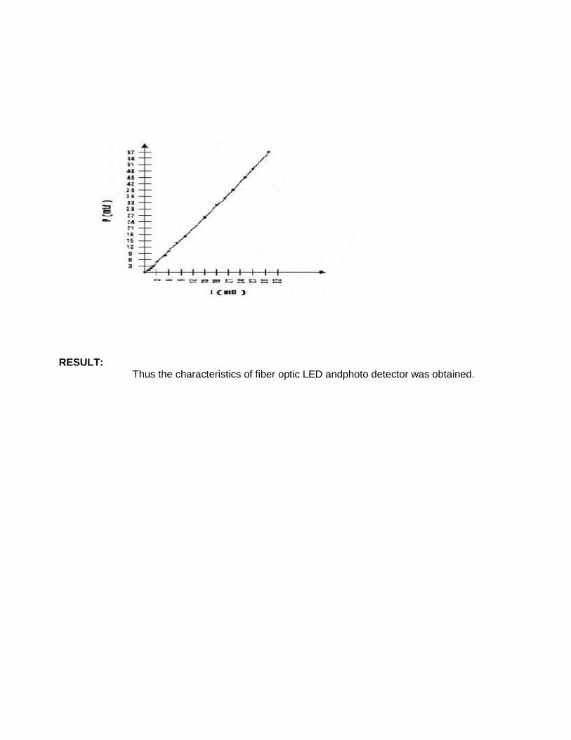
Measure the current flowing through Detector (RX1) SFH250V at corresponding optical power output
(Normally in u A).
We can observe that as incident optical power on detector increases, current flowing through the
detector increases.
BLOCK DIAGRAM:
RESULT: Thus the characteristics of fiber optic LED andphoto detector was obtained.
CONNECTORISATION OF JACKETED GLASS FIBER
Ex. No: 07
Date :
OBJECTIVE :
To study to terminate one meter of jacketed glass fiber with ST Connector at both the
ends. Measurement of Connectorisation Loss.
EQUIPMENTS:
1 meter Jacketed Glass Fiber.
CSK- Connector and Splice installation Kit
meter Standard Glass Patchchord
Optical Power Source.
Optical Power Meter
PROCEDURE:
PRECAUTIONS: Please note the following instructions carefully.
The Connectorisation Kit contains precision mechanical items. Handle the tools with great care.
Avoid direct skin contact with the chemicals. Irritation and sensitization might occur on contact,
wash areas immediately with water. Do not use solvents for washing in case of eye contact.
Wash with water for atleast Fifteen minutes and get medical attention.
Carry out the experiment in a dust-free & dry environment. During the process, absolute care
should be taken to keep the bare fiber free from impurities, in order to minimize losses.
Be careful to dispose of the chips of glass fiber while cutting.
Cut one meter of jacketed glass fiber optic cable. The fiber consists of core & clad of glass fiber,
buffer coating, fibrous (Kevlar) material and outer jacket.
Place the conical strain relief sleeve over the end of fiber such that broader end of sleeve should
be kept towards the fiber tip.
Remove the outer jacket coating of about ½ inch using fiber optic jacket stripper.
Cut the fibrous (Kevlar) material using blade or scissors.
Remove ½ inch of buffer coating using the fiber optic buffer stripper. Select the stripper hole of
smaller diameter while removing the buffer. The buffer coating can also be removed chemically.
Dip the fiber end in Methylene Chloride so that the coating get dissolved.
CAUTION: Care should be taken to avoid cutting the bare fiber of while trying to remove the outer and
buffer coating.
Wipe the bare fiber end with optic prep to remove the dust particles, which may have adhered to
the fiber. To minimize losses one should ensure to remove all traces of impurities.
Insert the fiber end into the connector and ensure that bare fiber emerges out from the ferrule of
the connector smoothly. Remove the fiber from the connector.
Take an equal amount of resin from each part of the epoxy and mix it thoroughly.
Apply a small amount of epoxy inside the housing of the connector and fill it completely using
syringe with needle.
Insert the stripped fiber into the connector and gently manipulate the cable without exerting any
pressure so that the bare fiber finally emerges from the ferrule. Ensure that all the extra part of
bare fiber should protrude out from the ferrule.
Clean the connector with cotton swabs to remove the additional epoxy that has came out of the
connector.
Allow the epoxy to cure for four hours. Take care that the position of the fiber remains unchanged
during this process. The fiber is not fixed in that position inside the connector. Curing process
can be accelerated by heating at 1400F for about one hour. One can use Hair dryer for this
purpose.
CAUTION: Care should be taken while applying epoxy to prevent any of it from reaching the
connector ferrule. This would block the hole in the ferrule face and render the connector useless.
Do not apply pressure while inserting the fiber in the connector. If the fiber breaks, pieces of glass
could clog the hole in the connector ferrule.
Crimp the back shell of the connector using the crimp tool. Care should be taken for selecting
the proper cavity diameter.
Slide the conical protective sleeve over the housing of the connector.
Cut the bare fiber part emerging out of the ferrule using the diamond scribe. Extreme care should
be taken while scribing and ensure that the cut is made perpendicularly and about 1 mm of the
fiber still protrude out of the ferrule.
Wipe the tip of the ferrule with optic prep.
Clean the Polishing pad and Polishing tool using tissue paper.
Place one sheet of polishing paper on the pad, taking care to avoid wrinkles and bubbles on the
sheet. If these sheets are not being used for the first time, ensure that there are no remnants of
glass or other impurities on them. Clean them with tissue paper if necessary.
Hold the connectorised fiber inside the ST polishing disc. This will ensure that the fiber is held at
900 while polishing. Rotate the disc over the polishing sheet in the manner of figure of eight
pattern. For about 40-50 times or more than that if required.
Observe the tip of the fiber under Microscope. Switch on the lights of microscope. Concentrate
the light beam on the ferrule. Turn the focusing wheel & zoom switch for better visibility. One can
view two concentric circle (core and clad) along with some dark spot.
Polish the fiber until there are no dark spot observed under the microscope. The core and the
clad regions should be clearly visible. The absence of this would mean that either the fiber has
slipped inside the ferrule while polishing as the bonding was inadequate or the fiber end has
broken inside ferrule, in which case the complete process should be repeated. The perfect mirror
finish will ensure maximum coupling of light through the fiber.
Repeat the above procedure to terminate the other end of the fiber.The ST connectorised
patchchord can now be used as a link between an optical transmitter and a optical receiver.
Another patchchord can be connected to this patchchord using an adapter.

MEASUREMENT OF CONNECTORISATION LOSS
PROCEDURE:
Take one meter standard glass Patchchord
Connect one end of the patchchord to optical power source and other end to optical power meter.
Switch on the power source and power meter. Select the wavelength in power meter in
accordance with the wavelength of the source.
Note the reading in power meter.
Replace the standard patchchord with the patchchord under test.
Note the reading in power meter and find out the difference of the readings.
The difference will denote connector loss.
RESULT: Thus the end of fiber optic cable is prepared to make joints between SJ connectors
And fiber to fiber.
STUDY OF MICROWAVE COMPONENTS
Ex. No: 08
Date :
OBJECTIVE :
To study the microwave components.
RECTANGULAR WAVEGUIDE:
Waveguides are manufactured to the highest mechanical and electrical standards and mechanical
tolerance to meet internal specifications, L and S band waveguides are fabricated by precision brazing of
brast plate and all other waveguides are in extrusion quality. Waveguide sections of specified length can be
supplied with flinges, painted outside and silver or gold plated inside.
VARIABLE ATTENUATOR:
Model 5020 is a simple and conveniently variable type set level attenuators to provide at least 20db
of continuously variable attenuation. These consist of a movable lossy vane inside the section of a
waveguide by means of a micrometer. The configuration of lossy vane is so designed to obtain the low
VSWR characteristics over the entire frequency band. These are meant for adjusting power levels and
isolating a source and load.
FREQUENCY METER MICROMETER TYPE:
Model 4055 are absorption type cavity wavemeter called frequency meter. These are made of
tunable resonant cavity of particular size. The cavity is connected to the source of energy through a section
of waveguide. The cavity absorbs some power at resonance, which is indicated as a sip in the output power.
The tuning of the cavity is achieved by means of a plunger connected to a Microcontroller. The readings of
the micrometer at resonance gives frequency from the calibration chart, provided calibration is normally
provided at 200Mhz internals.
TUNABLE PROBE:
Model 6055 tunable probes are designed for use with model 6051 slotted sections. These are meant
for exploring the energy of the electric field in a suitable fabricated section of the waveguide. The depth of
penetration into a waveguide section is adjustable by knob of the probe. The tip picks up the RF power from
the line and this power is rectified by crystal detector, which is then fed to the VSWR meter or indicating
instrument.
WAVEGUIDE DETECTOR MOUNT:
Model 4051 tunable detector mounts are simple and easy to use instruments for detecting microwave
power through a suitable detector. It consists of a detector crystal mounted in a section of waveguide and a
shorting plunging for matching purpose. The output of the crystal may be fed to and indicating instrument.
In K and R band detector mounts, the plunger is driven by a micrometer.
THREE PORT FERRITE CIRCULATOR:
Model 6021 and 6022 are T and Y type of the three port ferrite circulators respectively. These are
precisely machined and matched three port devices and these are meant for allowing microwave energy to
flow in clockwise direction with negligible loss but almost no transmission in anticlockwise direction.
Purpose and for measuring reflections and impedance. These consist of a section of waveguide thus making
it a four-part network. However, the fourth port is terminated with a matched load. These two parallel
sections are coupled to each other through many holes almost to give uniform coupling minimum frequency
sensitivity and high directivity. These are available in 3,6,10,20 and 40 db couplings.
E-PLANE BEND:
Model 7071 E-plane bends are fabricated from a section of waveguide to provide one 90° ± 1 bend
in E-plane. The cross section of bent waveguide is kept throughout uniform to give VSWR less than 1.05 or
1.08 or 1.02 over the entire frequency band. Bends other than 90° can also be fabricated.
KLYSTRON POWER SUPPLY:
Model KP-1010 power supply has been designed to operate low power klystrons such as 2K25, 756A,
RK5976 etc. Beam voltage may be continuously varied and is indicated on the front panel meter which can
be read the beam supply current and repeller supply volts also by changing the switch. Internal modulation
square waves with continuous variable frequency and amplitude are provided. An external modulation may
be used through the UHF(F) connector provided on front panel.
GUNN POWER SUPPLY: Model X-110 Gunn power supply comprises of a regulated DC power supply
and a square wave generator, designed to operate Gunn oscillator model 2151 or 2152 and pin modulate
model 451 respectively. The DC voltage is variable from 0 to 10v. The front panel meter monitors the
gunn voltage and the current drawn by the Gunn diode. The square waves of the generator are variable
from 0 to 10v in amplitude and 900 to 1100Hz in frequency. The power supply has been so designed to
protect Gunn diode from reverse voltage application, over transit and low frequency oscillators by negative
resistance of Gunn diode.
RESULT: Thus the various microwave components were studied.
CHARACTERISTICS OF GUNN DIODE OSCILLATOR
Ex. No: 09
Date :
OBJECTIVE :
To plot the characteristics of Gunn diode oscillator.
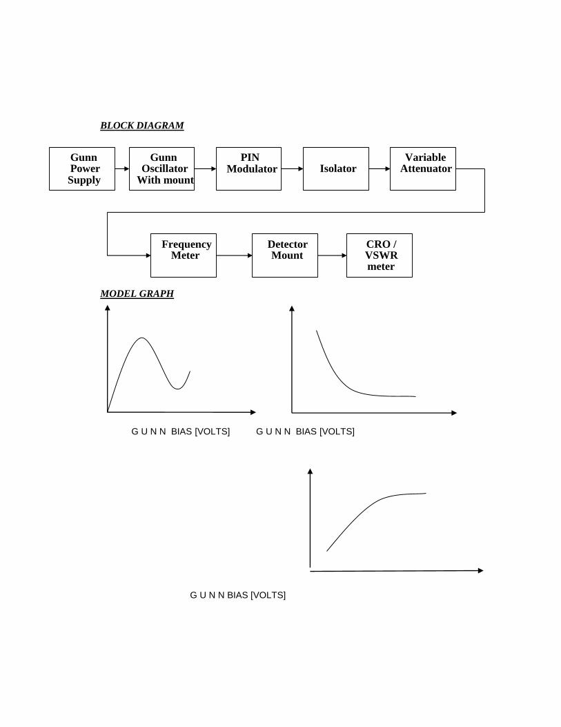
Apparatus/Components Required : 1. Gunn Power supply
2. Gunn oscillator with mount
3. PIN modulator
4. Isolator
5. Variable Attenuator
6. Frequency meter
7. Detector Mount
8. CRO
9. Probes
10. Cooling Fan
11. Stands
Theory :
Gunn diodes are made up of bulk semiconductor materials like Gallium Arsenide[GaAs],Indium
Phosphide[InP] and Cadmium Telluride[CdTe] which exhibit negative resistance. Initially for a range of bias
voltages the current increases with voltage and later starts decreasing with increase in bias voltage. In this
negative resistance region they exhibit Gunn effect or transfer electron effect and generates microwave
oscillatios. Gunn diode operates in 4 different modes viz. Gunn or TT mode,LSA mode, quenched domain
mode and delayed mode. Microwave oscillations are generated in Gunn or TT mode. A Gunn diode oscillator
is designed by mounting the diode inside a waveguide cavity formed by a short circuit termination at one end
and by an Iris at the other end.
Precautions :
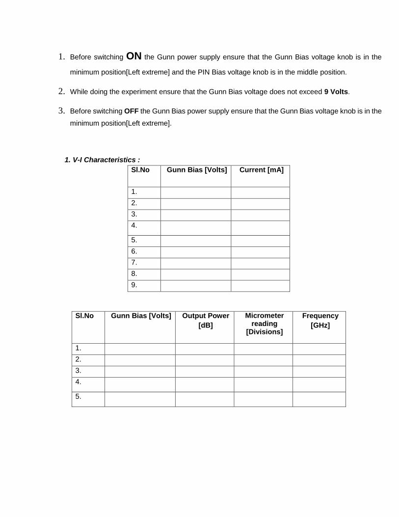
1. Before switching ON the Gunn power supply ensure that the Gunn Bias voltage knob is in the
minimum position[Left extreme] and the PIN Bias voltage knob is in the middle position.
2. While doing the experiment ensure that the Gunn Bias voltage does not exceed 9 Volts.
3. Before switching OFF the Gunn Bias power supply ensure that the Gunn Bias voltage knob is in the
minimum position[Left extreme].
1. V-I Characteristics :
Sl.No Gunn Bias [Volts] Current [mA]
1.
2.
3.
4.
5.
6.
7.
8.
9.
Sl.No Gunn Bias [Volts] Output Power
[dB]
Micrometer reading
[Divisions]
Frequency
[GHz]
1.
2.
3.
4.
5.
G U N N BIAS [VOLTS] G U N N BIAS [VOLTS]
G U N N BIAS [VOLTS]
BLOCK DIAGRAM
MODEL GRAPH
Gunn Power Supply
Gunn Oscillator
With mount
PIN Modulator
Isolator
Variable Attenuator
Frequency Meter
Detector Mount
CRO / VSWR meter
Procedure :
1. Obtain square wave output by setting the Gunn bias voltage around 6 volts or above and maximize the
output by adjusting the micrometers attached to the short-circuit plunger of the gunn diode mount and the
detector mount.
2. Now starting from 0 Volt vary the Gunn bias in steps of 1 Volt up to a maximum of 9 Volts. Note down the
corresponding currents from the milliammeter.
3. Tabulate the readings and plot the V-I characteristics.
4. In the region of oscillations i.e. for Gunn bias voltages in the range 6-9 Volts, for different bias voltages
tune the frequency meter and observe dip in the output and the corresponding micrometer position. After
noting down the micrometer reading, release[detune] the frequency meter and connect the detector output
to VSWR/POWER meter and note down the output power.
5. Tabulate the readings and plot the input-output characteristics[output power Vs Gunn bias voltage] and the
frequency response[Frequency Vs Gunn bias vltage].
Result :
Thus the characteristics of Gunn diode has been plotted
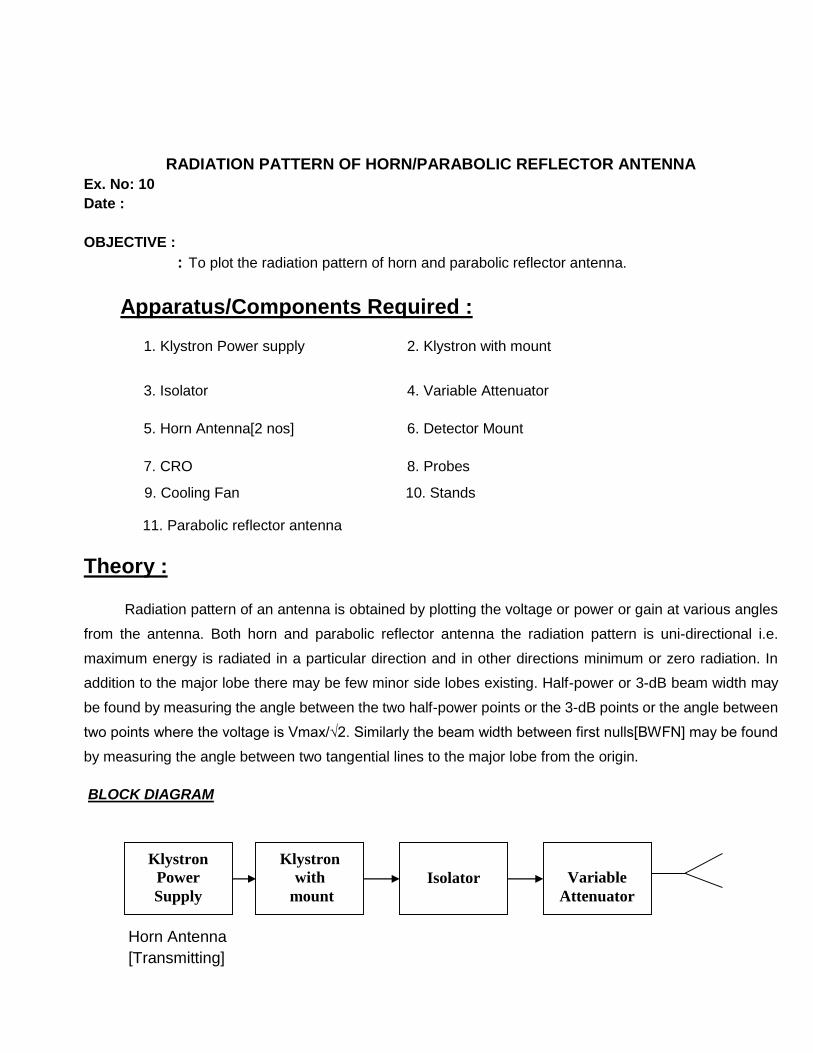
RADIATION PATTERN OF HORN/PARABOLIC REFLECTOR ANTENNA
Ex. No: 10
Date :
OBJECTIVE :
: To plot the radiation pattern of horn and parabolic reflector antenna.
Apparatus/Components Required :
1. Klystron Power supply
2. Klystron with mount
3. Isolator 4. Variable Attenuator
5. Horn Antenna[2 nos] 6. Detector Mount
7. CRO 8. Probes
9. Cooling Fan 10. Stands
11. Parabolic reflector antenna
Theory :
Radiation pattern of an antenna is obtained by plotting the voltage or power or gain at various angles
from the antenna. Both horn and parabolic reflector antenna the radiation pattern is uni-directional i.e.
maximum energy is radiated in a particular direction and in other directions minimum or zero radiation. In
addition to the major lobe there may be few minor side lobes existing. Half-power or 3-dB beam width may
be found by measuring the angle between the two half-power points or the 3-dB points or the angle between
two points where the voltage is Vmax/√2. Similarly the beam width between first nulls[BWFN] may be found
by measuring the angle between two tangential lines to the major lobe from the origin.
BLOCK DIAGRAM
Horn Antenna
[Transmitting]
Klystron Power
Supply
Klystron with
mount
Isolator
Variable
Attenuator
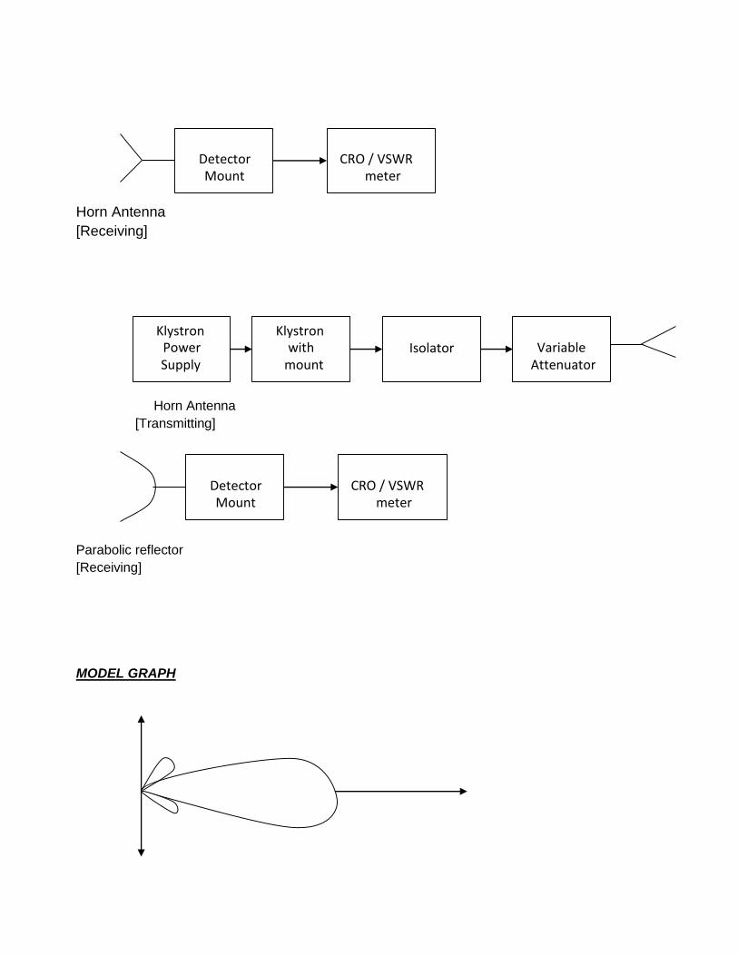
Horn Antenna
[Receiving]
Horn Antenna
[Transmitting]
Parabolic reflector
[Receiving]
MODEL GRAPH
Detector Mount
CRO / VSWR
meter
Klystron Power Supply
Klystron with
mount
Isolator
Variable
Attenuator
Detector Mount
CRO / VSWR
meter
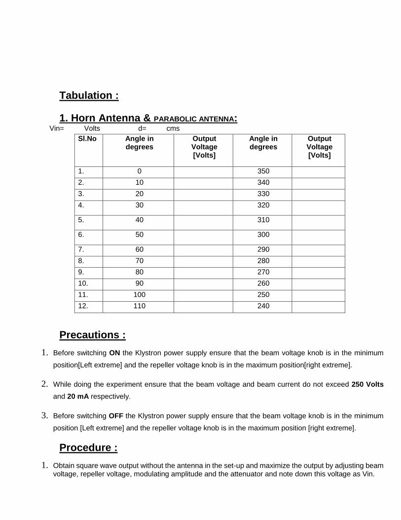
Tabulation :
1. Horn Antenna & PARABOLIC ANTENNA: Vin= Volts d= cms
Sl.No Angle in degrees
Output Voltage [Volts]
Angle in degrees
Output Voltage [Volts]
1. 0 350
2. 10 340
3. 20 330
4. 30 320
5. 40 310
6. 50 300
7. 60 290
8. 70 280
9. 80 270
10. 90 260
11. 100 250
12. 110 240
Precautions :
1. Before switching ON the Klystron power supply ensure that the beam voltage knob is in the minimum
position[Left extreme] and the repeller voltage knob is in the maximum position[right extreme].
2. While doing the experiment ensure that the beam voltage and beam current do not exceed 250 Volts
and 20 mA respectively.
3. Before switching OFF the Klystron power supply ensure that the beam voltage knob is in the minimum
position [Left extreme] and the repeller voltage knob is in the maximum position [right extreme].
Procedure :
1. Obtain square wave output without the antenna in the set-up and maximize the output by adjusting beam voltage, repeller voltage, modulating amplitude and the attenuator and note down this voltage as Vin.

2. Now connect the two horn antenna in the set-up and align the two antenna both vertically and horizontally for maximum output. Ensure a minimum distance(end to end) of 15 cms between the antenna.
3. Set the angle where maximum output obtained as zero degrees and note down the output voltage.
4. Vary the angle from zero degrees through 360 degrees and note down the corresponding output voltages. Tabulate the readings.
5. Plot the Output voltage Vs Angle in degrees in a polar sheet.
6. Find the 3dB beam width and BWFN.
7. Repeat steps 1 to 6 with parabolic reflector antenna in the receiving antenna position instead of horn antenna.
Result :
Thus the radiation pattern of horn and parabolic reflector antenna were plotted and the 3-dB beamwidth
and BWFN were found to be :
3-dB beamwidth = degrees
BWFN = degrees
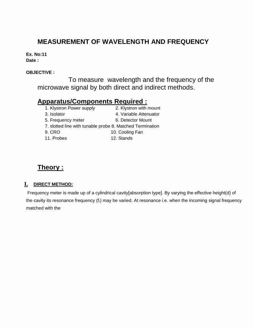
MEASUREMENT OF WAVELENGTH AND FREQUENCY
Ex. No:11
Date :
OBJECTIVE :
To measure wavelength and the frequency of the microwave signal by both direct and indirect methods.
Apparatus/Components Required : 1. Klystron Power supply 2. Klystron with mount
3. Isolator 4. Variable Attenuator
5. Frequency meter 6. Detector Mount
7. slotted line with tunable probe 8. Matched Termination
9. CRO 10. Cooling Fan
11. Probes 12. Stands
Theory :
I. DIRECT METHOD:
Frequency meter is made up of a cylindrical cavity[absorption type]. By varying the effective height(d) of
the cavity its resonance frequency (fr) may be varied. At resonance i.e. when the incoming signal frequency
matched with the
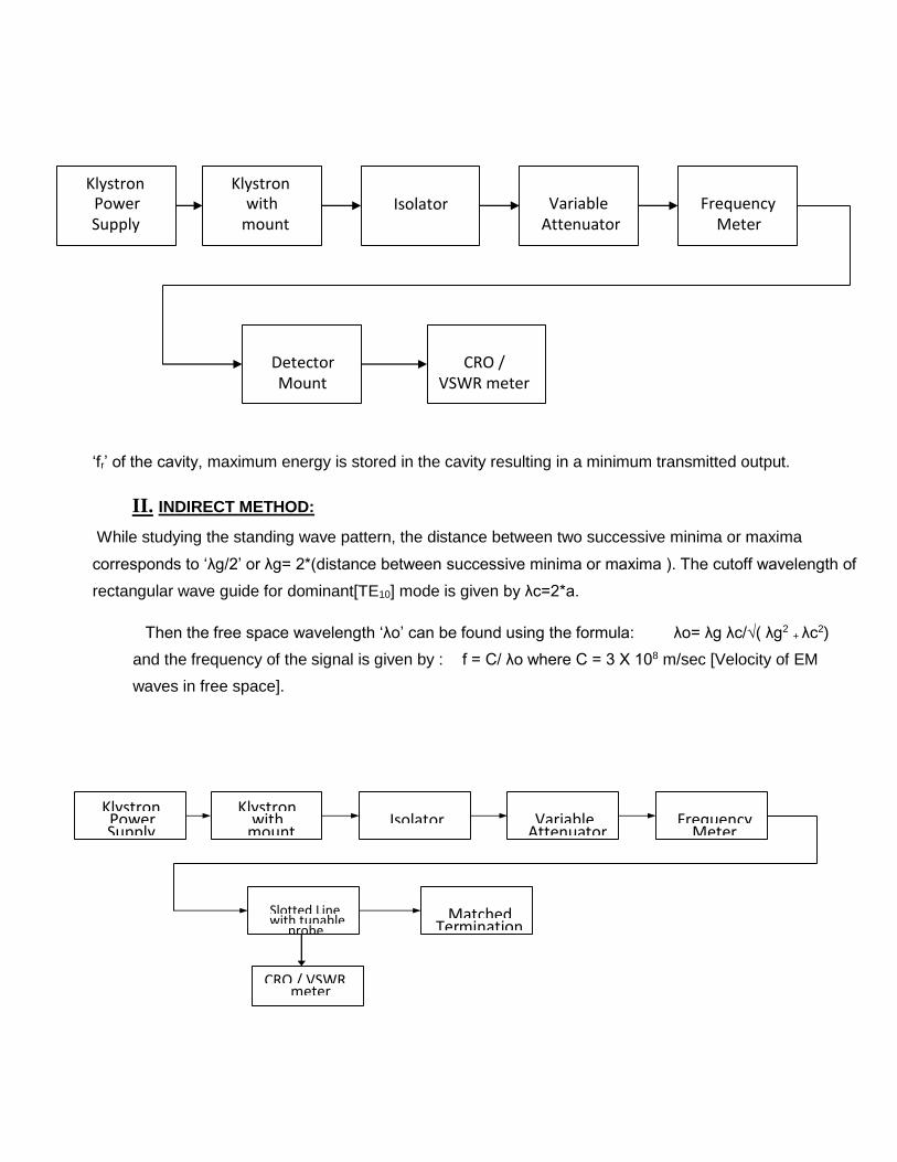
‘fr’ of the cavity, maximum energy is stored in the cavity resulting in a minimum transmitted output.
II. INDIRECT METHOD:
While studying the standing wave pattern, the distance between two successive minima or maxima
corresponds to ‘λg/2’ or λg= 2*(distance between successive minima or maxima ). The cutoff wavelength of
rectangular wave guide for dominant[TE10] mode is given by λc=2*a.
Then the free space wavelength ‘λo’ can be found using the formula: λo= λg λc/√( λg2 + λc2)
and the frequency of the signal is given by : f = C/ λo where C = 3 X 10⁸ m/sec [Velocity of EM
waves in free space].
Klystron Power Supply
Klystron with
mount
Isolator
Variable
Attenuator
Frequency
Meter
Detector Mount
CRO /
VSWR meter
CRO / VSWR meter
Klystron Power Supply
Klystron with
mount
Isolator
Variable
Attenuator
Frequency
Meter
Slotted Line with tunable
probe
Matched
Ter mination
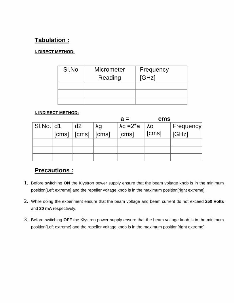
Tabulation :
I. DIRECT METHOD:
Sl.No Micrometer
Reading
Frequency
[GHz]
I. INDIRECT METHOD:
a = cms
Sl.No. d1
[cms]
d2
[cms]
λg
[cms]
λc =2*a
[cms]
λo [cms]
Frequency
[GHz]
Precautions :
1. Before switching ON the Klystron power supply ensure that the beam voltage knob is in the minimum
position[Left extreme] and the repeller voltage knob is in the maximum position[right extreme].
2. While doing the experiment ensure that the beam voltage and beam current do not exceed 250 Volts
and 20 mA respectively.
3. Before switching OFF the Klystron power supply ensure that the beam voltage knob is in the minimum
position[Left extreme] and the repeller voltage knob is in the maximum position[right extreme].
Procedure :
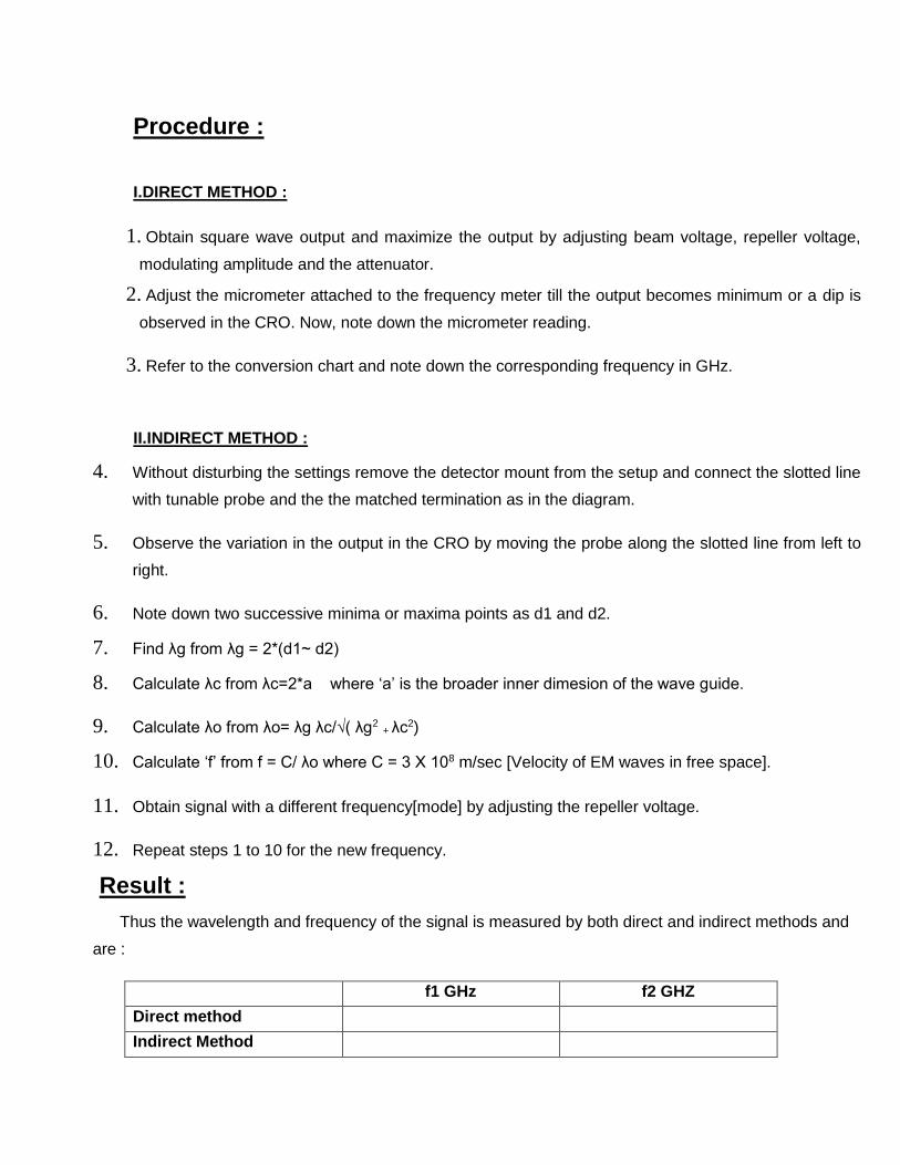
I.DIRECT METHOD :
1. Obtain square wave output and maximize the output by adjusting beam voltage, repeller voltage,
modulating amplitude and the attenuator.
2. Adjust the micrometer attached to the frequency meter till the output becomes minimum or a dip is
observed in the CRO. Now, note down the micrometer reading.
3. Refer to the conversion chart and note down the corresponding frequency in GHz.
II.INDIRECT METHOD :
4. Without disturbing the settings remove the detector mount from the setup and connect the slotted line
with tunable probe and the the matched termination as in the diagram.
5. Observe the variation in the output in the CRO by moving the probe along the slotted line from left to
right.
6. Note down two successive minima or maxima points as d1 and d2.
7. Find λg from λg = 2*(d1~ d2)
8. Calculate λc from λc=2*a where ‘a’ is the broader inner dimesion of the wave guide.
9. Calculate λo from λo= λg λc/√( λg2 + λc2)
10. Calculate ‘f’ from f = C/ λo where C = 3 X 10⁸ m/sec [Velocity of EM waves in free space].
11. Obtain signal with a different frequency[mode] by adjusting the repeller voltage.
12. Repeat steps 1 to 10 for the new frequency.
Result :
Thus the wavelength and frequency of the signal is measured by both direct and indirect methods and
are :
f1 GHz f2 GHZ
Direct method
Indirect Method
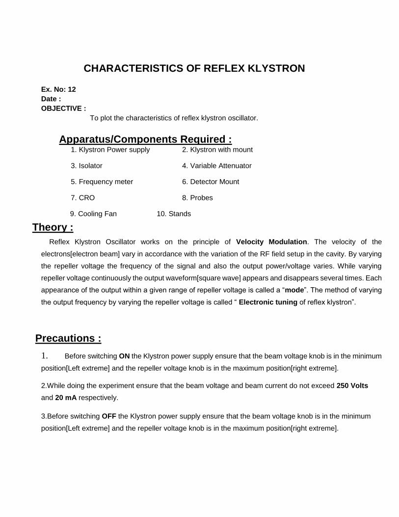
CHARACTERISTICS OF REFLEX KLYSTRON
Ex. No: 12
Date :
OBJECTIVE :
To plot the characteristics of reflex klystron oscillator.
Apparatus/Components Required : 1. Klystron Power supply 2. Klystron with mount
3. Isolator 4. Variable Attenuator
5. Frequency meter 6. Detector Mount
7. CRO 8. Probes
9. Cooling Fan 10. Stands
Theory :
Reflex Klystron Oscillator works on the principle of Velocity Modulation. The velocity of the
electrons[electron beam] vary in accordance with the variation of the RF field setup in the cavity. By varying
the repeller voltage the frequency of the signal and also the output power/voltage varies. While varying
repeller voltage continuously the output waveform[square wave] appears and disappears several times. Each
appearance of the output within a given range of repeller voltage is called a “mode”. The method of varying
the output frequency by varying the repeller voltage is called “ Electronic tuning of reflex klystron”.
Precautions :
1. Before switching ON the Klystron power supply ensure that the beam voltage knob is in the minimum
position[Left extreme] and the repeller voltage knob is in the maximum position[right extreme].
2.While doing the experiment ensure that the beam voltage and beam current do not exceed 250 Volts
and 20 mA respectively.
3.Before switching OFF the Klystron power supply ensure that the beam voltage knob is in the minimum
position[Left extreme] and the repeller voltage knob is in the maximum position[right extreme].
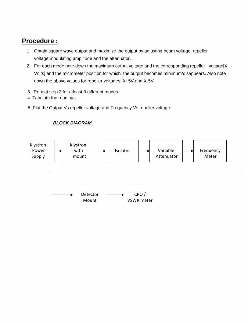
Procedure :
1. Obtain square wave output and maximize the output by adjusting beam voltage, repeller
voltage,modulating amplitude and the attenuator.
2. For each mode note down the maximum output voltage and the corresponding repeller voltage[X
Volts] and the micrometer position for which the output becomes minimum/disappears. Also note
down the above values for repeller voltages: X+5V and X-5V.
3. Repeat step 2 for atleast 3 different modes.
4. Tabulate the readings.
5. Plot the Output Vs repeller voltage and Frequency Vs repeller voltage.
BLOCK DIAGRAM
Klystron Power Supply
Klystron with
mount
Isolator
Variable
Attenuator
Frequency
Meter
Detector Mount
CRO /
VSWR meter
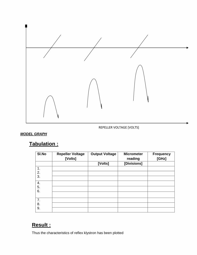
MODEL GRAPH
Tabulation :
Sl.No Repeller Voltage
[Volts]
Output Voltage Micrometer
reading
Frequency
[GHz]
[Volts] [Divisions]
1. 2. 3.
4. 5. 6.
7. 8. 9.
Result :
Thus the characteristics of reflex klystron has been plotted
REPELLER VOLTAGE [VOLTS]
STUDY OF DIRECTIONAL COUPLER
Ex. No: 13
Date :
OBJECTIVE :
To study the characteristics of directional coupler and find its S-matrix.
APPARATUS REQUIRED:
1. Klystron Power supply 2. Klystron with mount
3. Isolator 4. Variable Attenuator
5. Frequency meter 6. Slotted line with tunable probe
7. Matched Termination__ Nos 8. Directional Coupler
9. VSWR meter 10. CRO
11. Stands 12. Probes
13. Cooling Fan
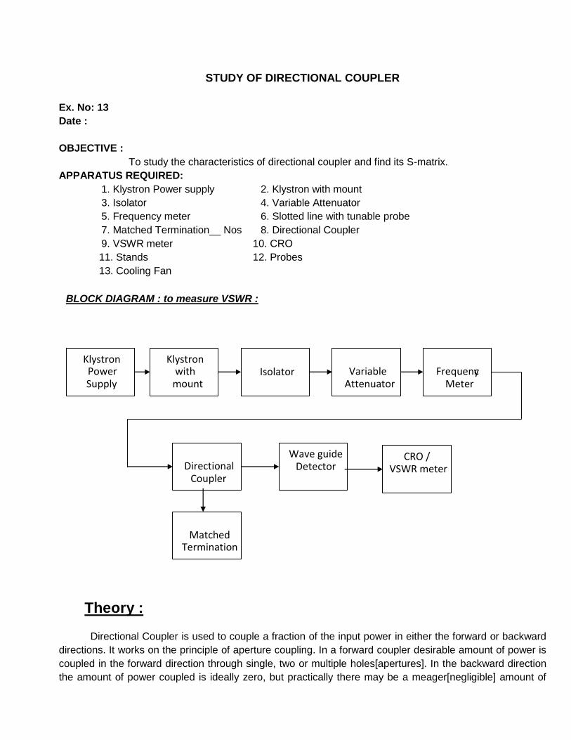
BLOCK DIAGRAM : to measure VSWR :
Theory :
Directional Coupler is used to couple a fraction of the input power in either the forward or backward
directions. It works on the principle of aperture coupling. In a forward coupler desirable amount of power is
coupled in the forward direction through single, two or multiple holes[apertures]. In the backward direction
the amount of power coupled is ideally zero, but practically there may be a meager[negligible] amount of
Klystron Power Supply
Klystron with
mount
Isolator
Variable
Attenuator
Frequenc y
Meter
Directional
Coupler
Wave guide Detector
Matched
Termination
CRO / VSWR meter
power which is absorbed by the matched termination connected internally. Hence practically it remains a
closed port. Ideal values for the parameters are as below :
Main line VSWR = 1
Transmission loss = 10 log[P1/P2] = 20 log[V1/V2] = 0 dB
Coupling coefficient = 10 log[P1/P4]=20 log[V1/V4] is a design parameter
Directivity = 10 log[P4/P3] = 20 log[V4/V3] = ∞ dB
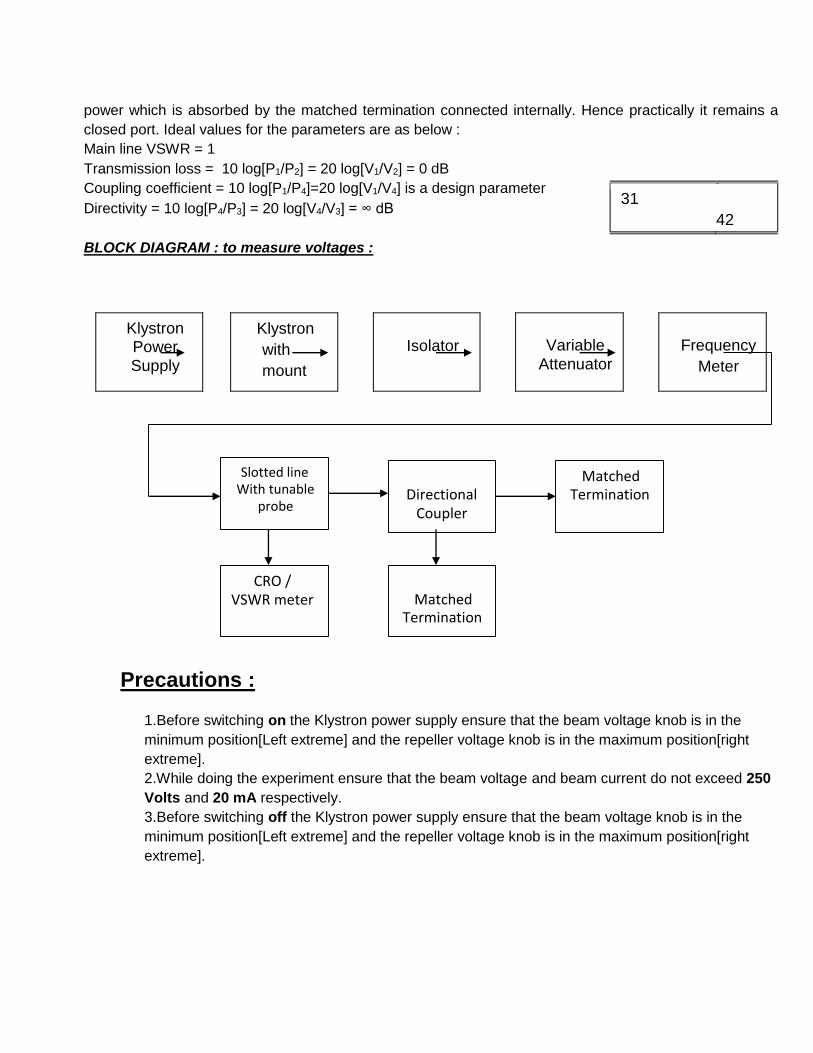
BLOCK DIAGRAM : to measure voltages :
Precautions :
1.Before switching on the Klystron power supply ensure that the beam voltage knob is in the
minimum position[Left extreme] and the repeller voltage knob is in the maximum position[right
extreme].
2.While doing the experiment ensure that the beam voltage and beam current do not exceed 250
Volts and 20 mA respectively.
3.Before switching off the Klystron power supply ensure that the beam voltage knob is in the
minimum position[Left extreme] and the repeller voltage knob is in the maximum position[right
extreme].
31
42
Klystron Power
Supply
Klystron
with
mount
Isolator
Variable
Attenuator
Frequency
Meter
Directional
Coupler
Matched Terminatio n
Matched
Termination
Slotted line With tunable
probe
CRO / VSWR meter
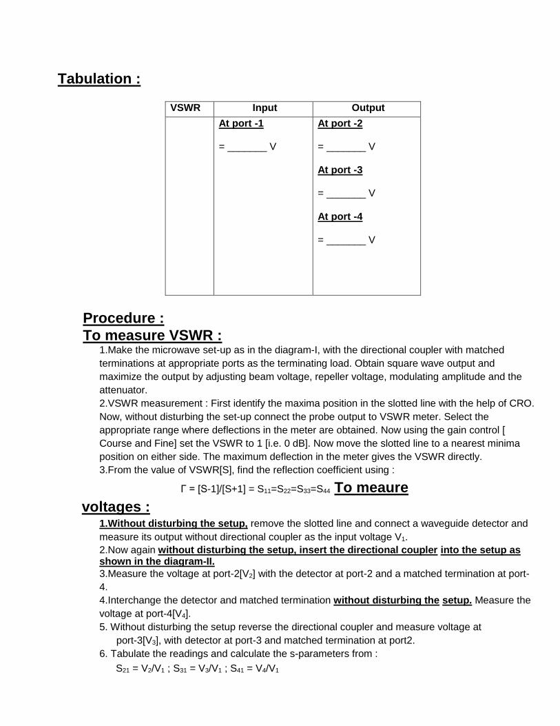
Tabulation :
Procedure :
To measure VSWR : 1.Make the microwave set-up as in the diagram-I, with the directional coupler with matched
terminations at appropriate ports as the terminating load. Obtain square wave output and
maximize the output by adjusting beam voltage, repeller voltage, modulating amplitude and the
attenuator.
2.VSWR measurement : First identify the maxima position in the slotted line with the help of CRO.
Now, without disturbing the set-up connect the probe output to VSWR meter. Select the
appropriate range where deflections in the meter are obtained. Now using the gain control [
Course and Fine] set the VSWR to 1 [i.e. 0 dB]. Now move the slotted line to a nearest minima
position on either side. The maximum deflection in the meter gives the VSWR directly.
3.From the value of VSWR[S], find the reflection coefficient using :
Γ = [S-1]/[S+1] = S11=S22=S33=S44 To meaure
voltages :
1.Without disturbing the setup, remove the slotted line and connect a waveguide detector and
measure its output without directional coupler as the input voltage V1.
2.Now again without disturbing the setup, insert the directional coupler into the setup as shown in the diagram-II.
3.Measure the voltage at port-2[V2] with the detector at port-2 and a matched termination at port-
4.
4.Interchange the detector and matched termination without disturbing the setup. Measure the
voltage at port-4[V4].
5. Without disturbing the setup reverse the directional coupler and measure voltage at
port-3[V3], with detector at port-3 and matched termination at port2.
6. Tabulate the readings and calculate the s-parameters from :
S21 = V2/V1 ; S31 = V3/V1 ; S41 = V4/V1
VSWR Input Output
At port -1 = _______ V
At port -2 = _______ V
At port -3 = _______ V
At port -4
= _______ V

Transmission loss[T] in dB = 20 log [1/S21]
Coupling Coefficient [C] in dB = 20 log [1/S31] and
Directivity [D] in dB = 20 log [S41/S31]
Result :
The characteristics of directional coupler is studied and the S – parameters and the other parameters are
found as below:
S11 S21 S31 S41
Transmission Loss
[dB]
Coupling Coefficient
[dB]
Directivity [dB]
VSWR MEASUREMENT
Ex. No: 14
Date :
OBJECTIVE :
To measure VSWR introduced by the wave guide in dominant mode of propagation.
COMPONENTS REQUIRED:
1. Microwave source (klystron power supply)
2. Klystron Mount
3. Isolator
4. Variable Attenuator
5. Slotted section
6. Matched Termination
7. VSWR meter (or) CRO
FORMULA: VSWR = V max / V min
Precautions : 1.Before switching on the Klystron power supply ensure that the beam voltage knob is in the minimum
position[Left extreme] and the repeller voltage knob is in the maximum position[right extreme].
2.While doing the experiment ensure that the beam voltage and beam current do not exceed 250 Volts and
20 mA respectively.
3.Before switching off the Klystron power supply ensure that the beam voltage knob is in the minimum
position[Left extreme] and the repeller voltage knob is in the maximum position[right extreme].
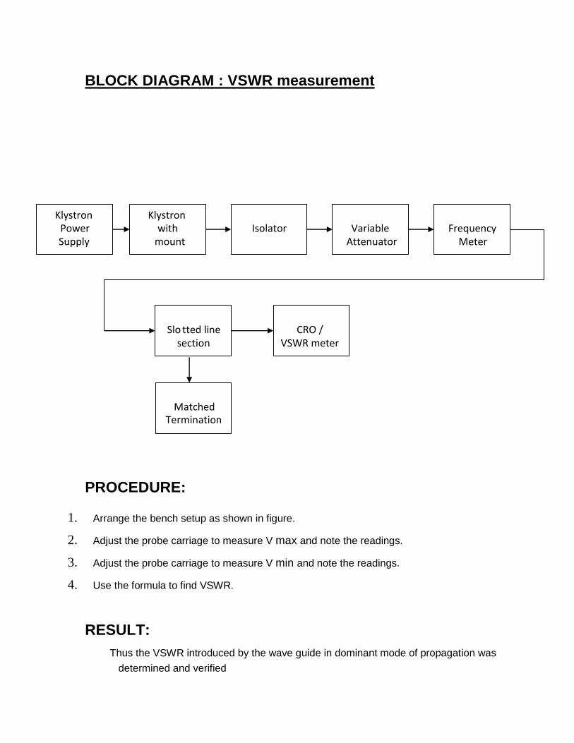
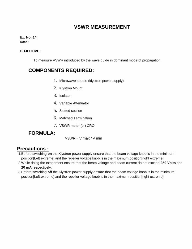
BLOCK DIAGRAM : VSWR measurement
PROCEDURE:
1. Arrange the bench setup as shown in figure.
2. Adjust the probe carriage to measure V max and note the readings.
3. Adjust the probe carriage to measure V min and note the readings.
4. Use the formula to find VSWR.
RESULT:
Thus the VSWR introduced by the wave guide in dominant mode of propagation was
determined and verified
Klystron Power Supply
Klystron with
mount
Isolator
Variable
Attenuator
Frequency
Meter
Slo tted line
section
CRO /
VSWR meter
Matched
Termination
ATTENUATION AND POWER MEASUREMENT
Ex. No: 15
Date :
OBJECTIVE :
To measure the output of a variable attenuator and to verify its attenuation characteristics.
APPARATUS REQUIRED:
Klystron power supply, Klystron with mount, Isolator, Variable attenuator, Frequency meter,
Detector mount, CRO, cooling fan, probes, stands
PRECAUTIONS:
1.Before switching on the klystron power supply ensure that beam voltage knob and repeller
voltage knob are in the min and max position respectively.
2. At no point should voltage or current exceed 250 mA and 20mA respectively.
3. Ensure that knobs are at the original position before switching off.
THEORY:
THERMOCOUPLE:
Thermocouples are based on the fact that dissimilar metals generate a voltage due to temperature difference at a hot and a cold junction of the two metals. The increased density of free electrons at the left causes diffusion towards the right. The migration of electrons towards the right is by diffusion, the same physical phenomenon that tends to equalize the partial pressure of a gas throughout the space. The rod reached equilibrium when the rightward force of heat induced diffusion.
MODERN POWER METER:
A 16- bit analog digital converter (ADC) processes the average power signal. A highly sophisticated video amplifier design is implemented for the normal path to pressure envelop fidelity and accuracy. The central gun for peak and average power meters is to provide reliable accurate and fast characteristics of pulsed and complex modulation envelops. The meters excel in versatility featuring a techniques called time gated measurements.
BLOCK DIAGRAM : ATTENUATION MEASUREMENT
Klystron Power Supply
Klystron with
mount
Isolator
Variable
Attenuator
Frequency
Meter
Detector mount
CRO /
VSWR meter
Klystron Power Supply
Klystron with
mount
Isolator
Variable
Attenuator
Frequency
Meter
Device under
Test
Detector mount
CRO /
VSWR meter

PROCEDURE:
1. Set the micro bench as per the block diagram.
2. Initial setting in the power meter is set.
3. Resolution→ 0.1 db]
4. Select absolute unit option and select dbm.
5. Select bar graph required.
6. Select the band as X
7. Select the number of samples/sec as 100/sec.
8. Enter the switch, which is used to store the selected mean option.
9. Escape switch is used to cancel any command.
10. The maximum output power is obtained by properly adjusting the klystron power supply.
11. By varying the variable attenuator corresponding output power is measured from the power meter.
12. A graph is drawn between micrometer reading of VA and power meter.
RESULT:
Thus the output of a variable attenuator was measured and its characteristics were verified.