Embed Size (px)
Citation preview
ELECTRONICS SYSTEMELECTRONICS SYSTEM DESIGN
SECTION 2SECTION-2
LSI AND MSI CIRCUITS AND THEIR APPLICATIONSTHEIR APPLICATIONS
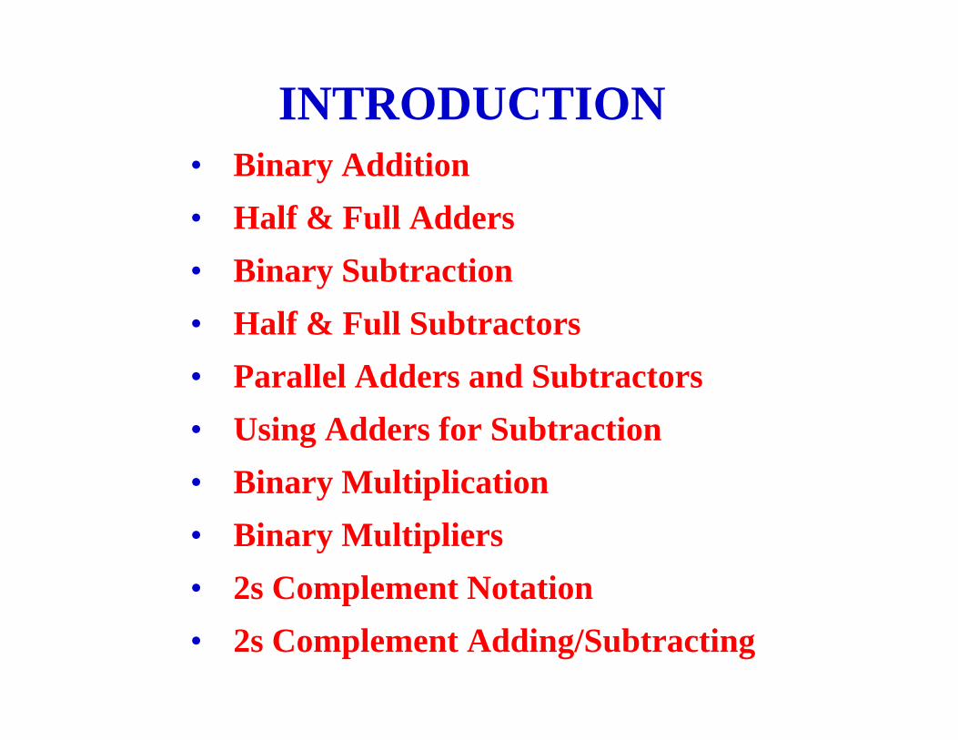
INTRODUCTION• Binary Addition• Half & Full Adders• Binary Subtraction• Half & Full Subtractors• Half & Full Subtractors• Parallel Adders and Subtractors• Using Adders for Subtraction• Binary Multiplication• Binary Multipliers• 2s Complement Notationp• 2s Complement Adding/Subtracting
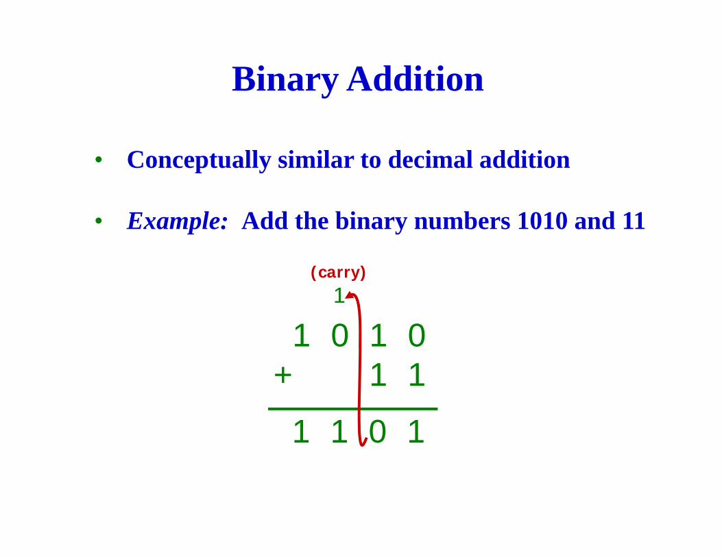
Binary Addition
• Conceptually similar to decimal addition
• Example: Add the binary numbers 1010 and 11
(carry)1
1 0 1 0+ 1 1+ 1 1
1011
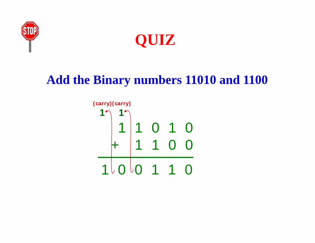
QUIZ
Add h Bi b 11010 d 1100
QU
Add the Binary numbers 11010 and 1100
(carry)(carry)
1 1 0 1 0
( y)
1( y)
1
+ 1 1 0 0
011001 011001
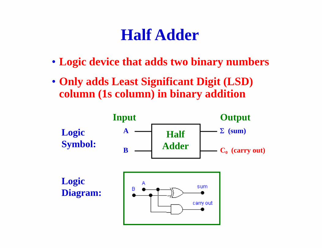
Half Adder• Logic device that adds two binary numbers
• Only adds Least Significant Digit (LSD) column (1s column) in binary addition
A Σ (sum)Half
Input OutputLogic
B C0 (carry out)AdderSymbol:
Logic Diagram:
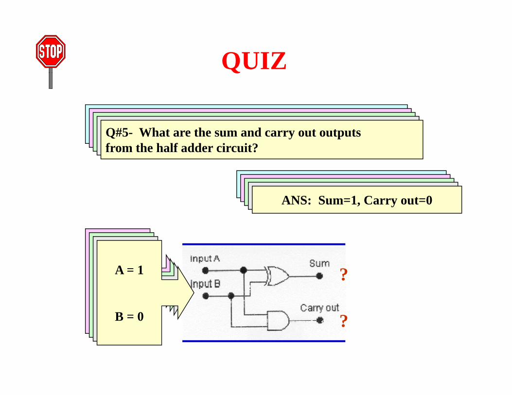
QUIZQ
Q#1 This circuit is called aQ#2- What are the sum and carry out outputsQ#3 What are the sum and carry out outputsQ#1- This circuit is called a ___.Q#2 What are the sum and carry out outputsfrom the half adder circuit?Q#3- What are the sum and carry out outputsfrom the half adder circuit?Q#4- What are the sum and carry out outputsfrom the half adder circuit?Q#5- What are the sum and carry out outputsfrom the half adder circuit?
ANS: Half-adderANS: Sum=0, Carry out=0ANS: Sum=1, Carry out=0ANS: Sum=0, Carry out=1ANS: Sum=1, Carry out=0
?A = 0A = 0A = 1A = 1 ?
?B = 0B = 1B = 1
A 1
B = 0 ?
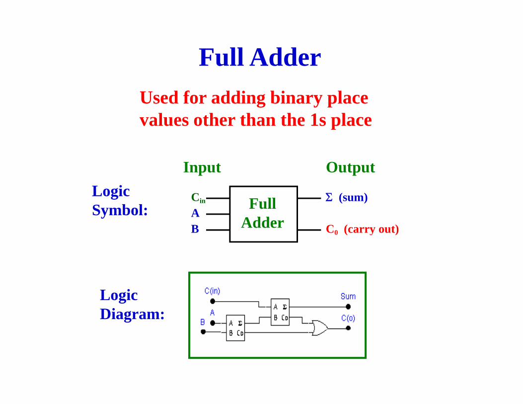
Full AdderUsed for adding binary place values other than the 1s placevalues other than the 1s place
Input OutputLogic Symbol: A
B
Σ (sum)
C (carry out)
FullAdder
Cin
B C0 (carry out)Adder
Logic Diagram:
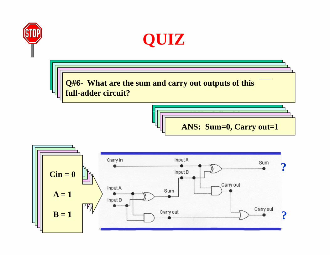
QUIZQ
Q#1- This combinational logic circuit is described as a(n) .Q#2- What are the sum and carry out outputs of thisQ#3- What are the sum and carry out outputs of thisQ#4- What are the sum and carry out outputs of thisQ#5 What are the sum and carry out outputs of thisQ g ( ) ___
ANS f ll dd
full-adder circuit?Q y pfull-adder circuit?Q#4 What are the sum and carry out outputs of thisfull-adder circuit?Q#5- What are the sum and carry out outputs of thisfull-adder circuit?Q#6- What are the sum and carry out outputs of thisfull-adder circuit?
ANS: full-adderANS: Sum=0, Carry out=0ANS: Sum=1, Carry out=0ANS: Sum=0, Carry out=1ANS: Sum=1, Carry out=1ANS: Sum=0, Carry out=1
?Cin = 0Cin = 0Cin = 1Cin = 1Cin = 0A = 0
B = 0
A = 0
B = 1
A = 0
B 1
A = 1
Cin 0
A = 1
?B 1B = 1B = 1B = 1
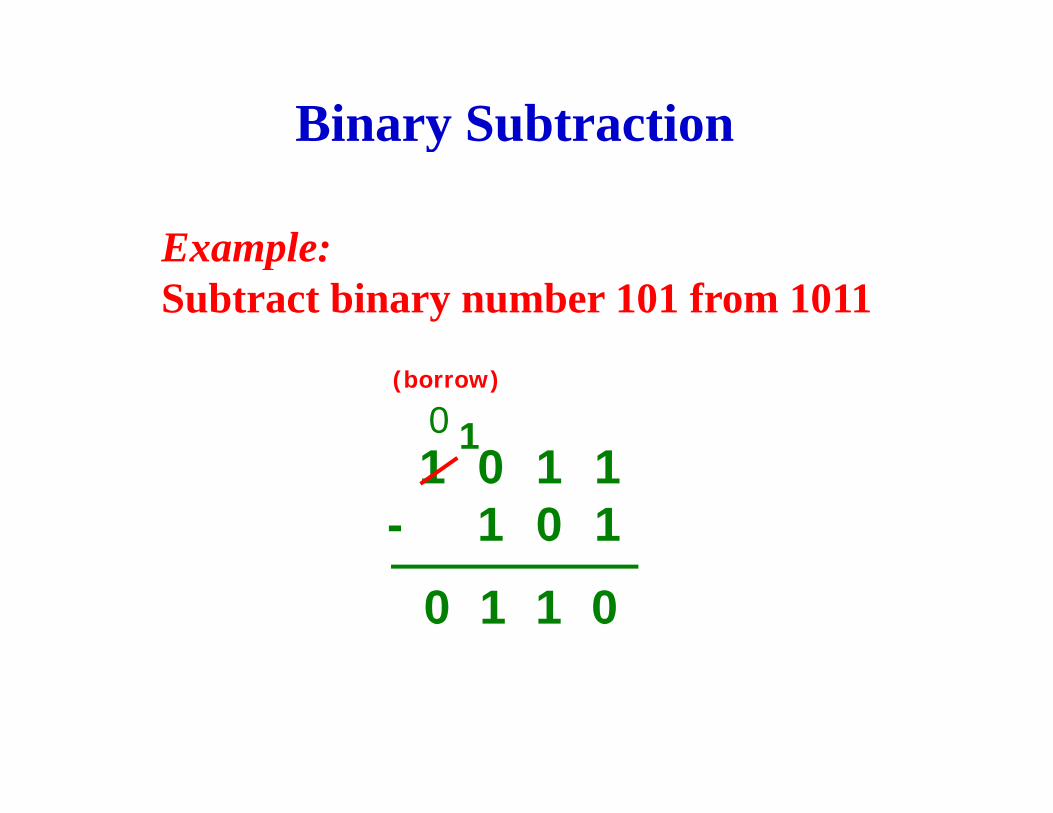
Binary Subtraction
Example:
y
Example: Subtract binary number 101 from 1011
1 0 1 1
(borrow)
101 0 1 1
- 1 0 1
0110
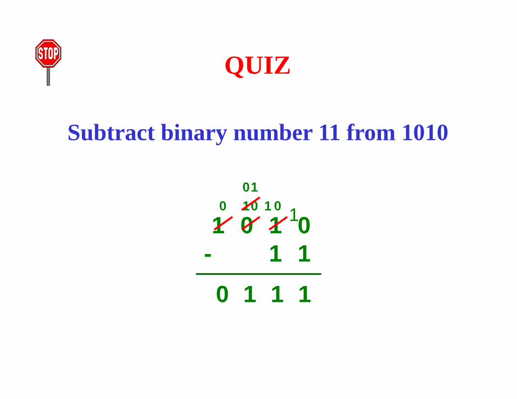
QUIZQU
Subtract binary number 11 from 1010
1 0 1 01100 001
1
1 0 1 0- 1 1
1110
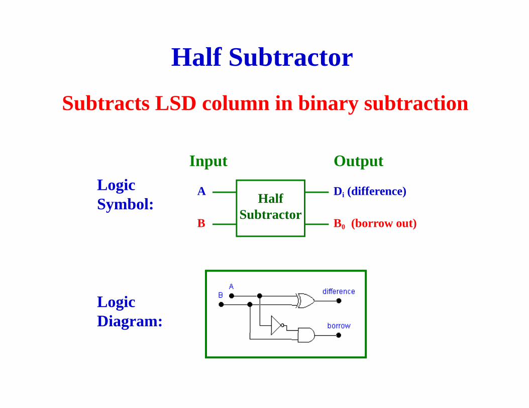
Half Subtractor
Subtracts LSD column in binary subtraction
Input Output
A
B
Di (difference)
B0 (borrow out)
HalfSubtractor
Logic Symbol:
Logic Diagram:
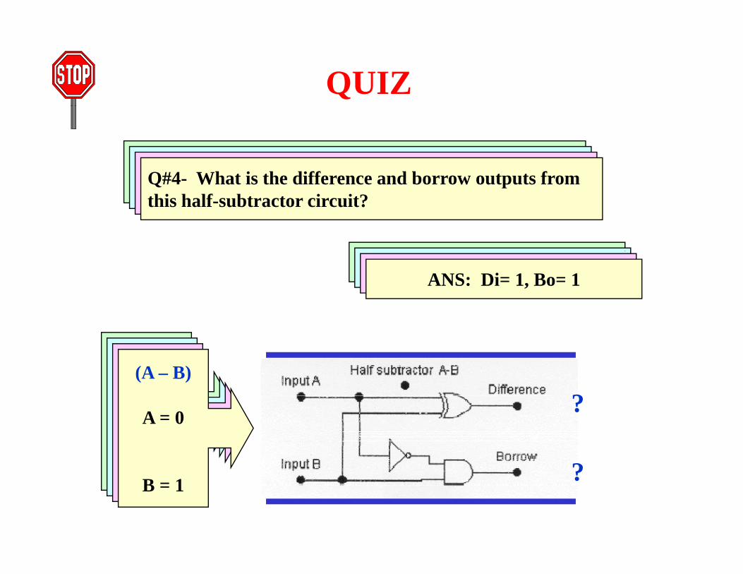
QUIZ
Q#1- What is the difference and borrow outputs fromThi h lf bt t i it?Q#2- What is the difference and borrow outputs fromQ#3- What is the difference and borrow outputs fromQ#4 What is the difference and borrow outputs fromThis half-subtractor circuit?this half-subtractor circuit?Q#3 What is the difference and borrow outputs fromthis half-subtractor circuit?Q#4- What is the difference and borrow outputs fromthis half-subtractor circuit?
ANS: Di= 0, Bo= 0ANS: Di= 1, Bo= 0ANS: Di= 0, Bo= 0ANS: Di= 1, Bo= 1
?
(A – B)
A 0
(A – B)(A – B)(A – B)
?
?
A = 0
B = 0
A = 1
B 0
A = 1A = 0
?B = 0B = 0B = 1B = 1
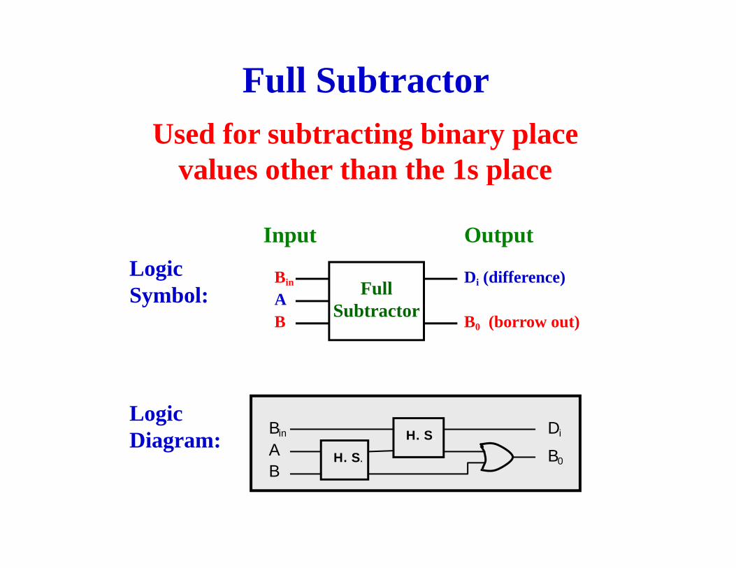
Full SubtractorUsed for subtracting binary place
values other than the 1s placevalues other than the 1s place
Input OutputLogic Symbol: A
B
Di (difference)
B (borrow out)
FullSubtractor
Bin
B B0 (borrow out)
Logic Diagram: A
Di
B0H. S.
H. S.Bin
B0
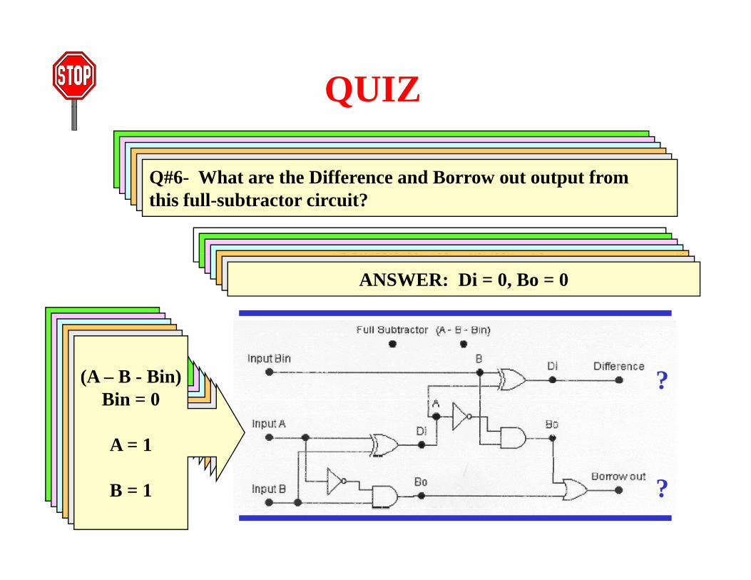
QUIZQQ#1- What are the Difference and Borrow out output fromthis full-subtractor circuit?Q#2- What are the Difference and Borrow out output fromthis full-subtractor circuit?Q#3- What are the Difference and Borrow out output fromthis full subtractor circuit?Q#4- What are the Difference and Borrow out output fromQ#5- What are the Difference and Borrow out output fromQ#6- What are the Difference and Borrow out output from
HINT: truth table from textbook (Fig. 10-10) is helpfulANSWER: Di = 0 Bo = 0
this full subtractor circuit?
ANSWER Di 1 B 1
this full-subtractor circuit?this full-subtractor circuit?Q pthis full-subtractor circuit?Q#6 What are the Difference and Borrow out output fromthis full-subtractor circuit?
( g ) pANSWER: Di 0, Bo 0ANSWER: Di = 1, Bo = 1ANSWER: Di = 1, Bo = 1ANSWER: Di = 0, Bo = 1ANSWER: Di = 1, Bo = 0ANSWER: Di = 0, Bo = 0
?(A – B - Bin)
Bin = 0(A – B - Bin)
Bin = 1(A – B - Bin)
Bin = 1(A – B - Bin)
Bin = 1(A – B - Bin)
Bin = 0(A – B - Bin)
Bin = 0A = 0
B = 0
A = 0
B = 0
A = 1
B = 1
A = 0
B 1
0
A = 1
Bin = 0
A = 1
?B 0B = 1B = 1B = 0B = 1
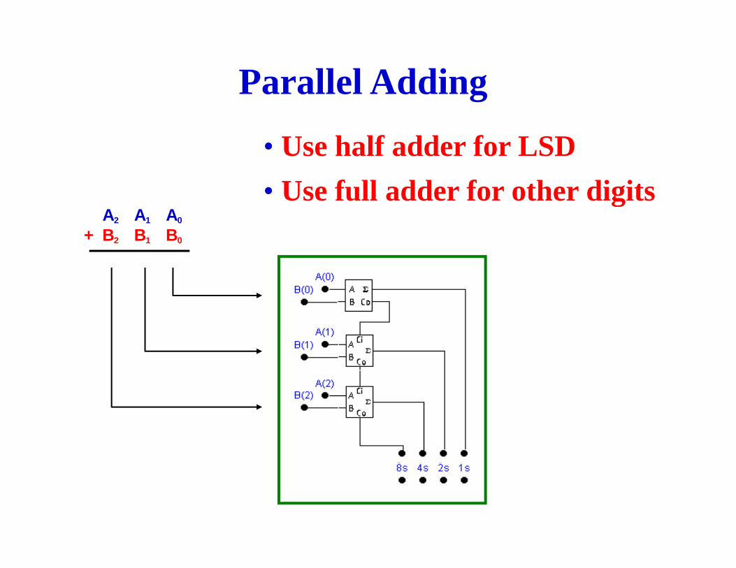
Parallel Adding
• Use half adder for LSD• Use full adder for other digits
A2 A1 A0
+ B2 B1 B0
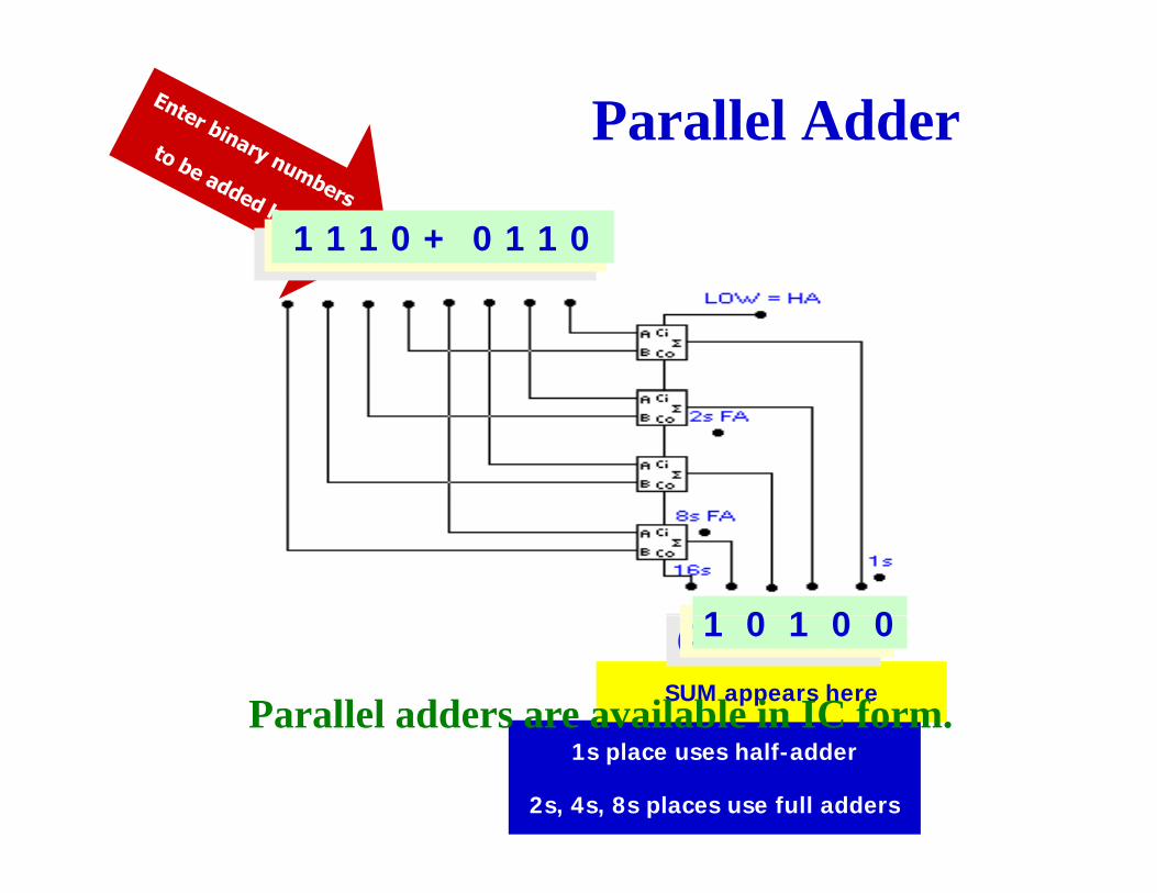
Parallel Adder
0 0 1 1 + 1 0 0 01 1 0 0 + 1 1 1 11 1 1 0 + 0 1 1 0
1 0 1 0 0
SUM appears here
0 1 0 1 11 1 0 1 11 0 1 0 0
Parallel adders are available in IC form.1s place uses half-adder
2s, 4s, 8s places use full adders
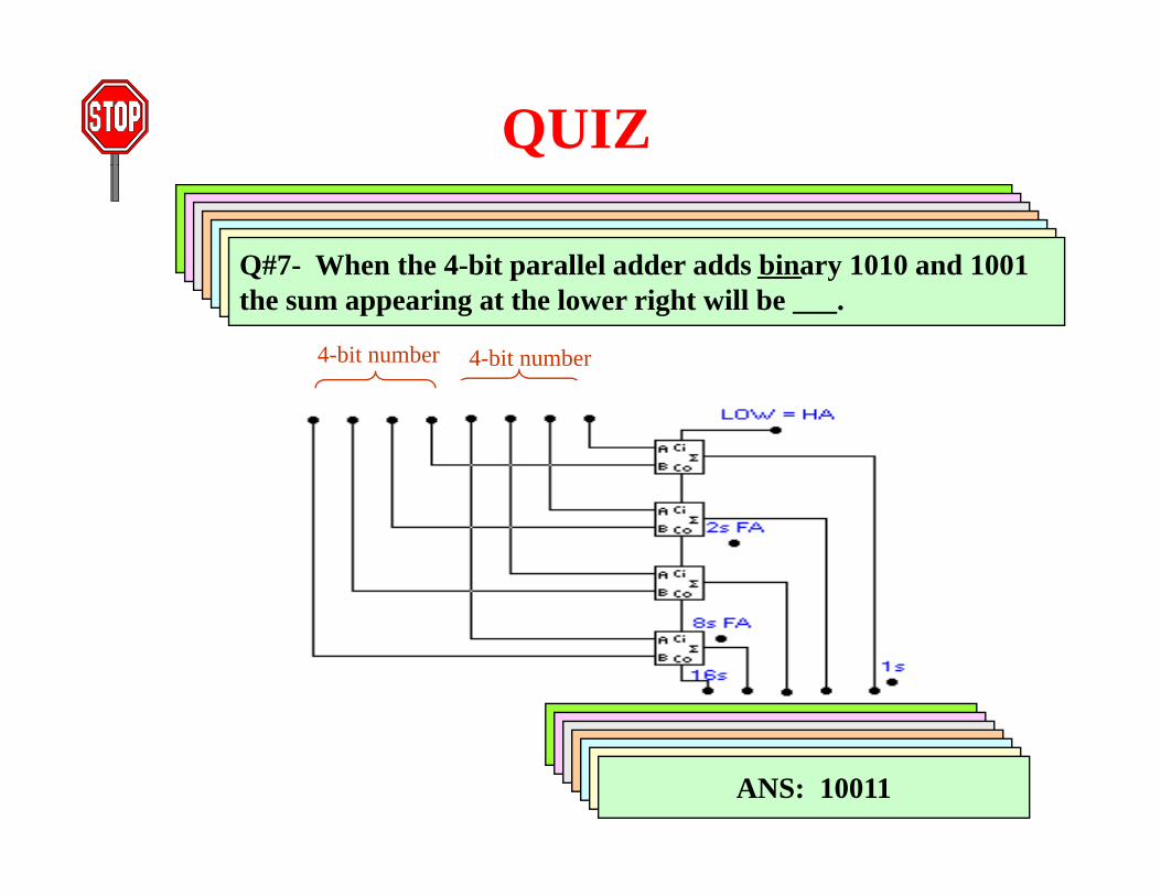
QUIZQ#1- With the top full adder’s Cin input LOW, this operatesas a half-adder while the bottom three are full adders. (T or F)Q#2- When the 4-bit parallel adder adds binary 1100 and 0011the sum appearing at the lower right will be ___. Q#3- When the 4-bit parallel adder adds binary 0111 and 1001the sum appearing at the lower right will be . Q#4- When the 4-bit parallel adder adds binary 1101 and 1001the sum appearing at the lower right will beQ#5- When the 4-bit parallel adder adds binary 0011 and 0110the sum appearing at the lower right will beQ#6- When the 4-bit parallel adder adds binary 1111 and 1111Q#7- When the 4-bit parallel adder adds binary 1010 and 1001
4-bit number 4-bit number
pp g g ___the sum appearing at the lower right will be ___. the sum appearing at the lower right will be ___. the sum appearing at the lower right will be ___. Q p ythe sum appearing at the lower right will be ___.
ANS TANS: TrueANS: 01111ANS: 10000ANS: 10110ANS: 01001ANS: 11110ANS: 10011
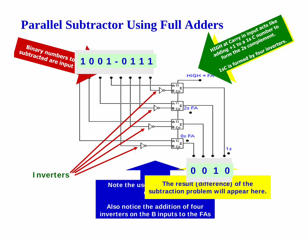
Parallel Subtractor Using Full Adders
1 1 1 1 - 0 0 1 11 0 0 1 - 0 1 1 1
Note the use of four full adder circuits
InvertersThe result (difference) of the
subtraction problem will appear here.
1 1 0 00 0 1 0
circuits
Also notice the addition of four inverters on the B inputs to the FAs
p pp
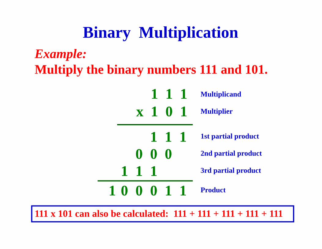
Binary MultiplicationExample: Multiply the binary numbers 111 and 101.
1 1 11 0 1
Multiplicand
M l i li
111
x 1 0 1 Multiplier
1st partial product111000
1112nd partial product
3rd partial product111110001
3rd partial product
Product
111 x 101 can also be calculated: 111 + 111 + 111 + 111 + 111
QUIZ
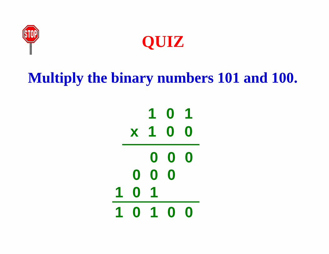
Multiply the binary numbers 101 and 100
QU
Multiply the binary numbers 101 and 100.
1 0 11 0 1x 1 0 0
000000 000
10100101 00101
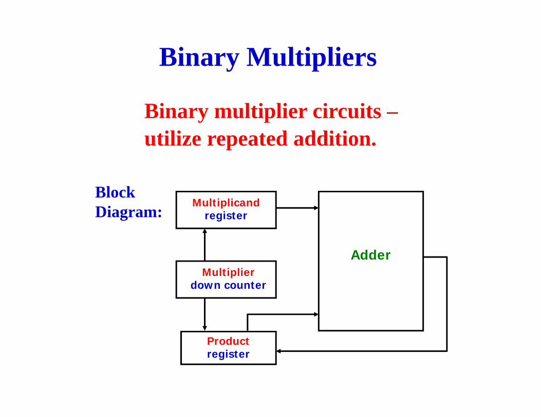
Binary Multipliers
Binary multiplier circuits –utilize repeated addition.
Block Diagram:
Multiplicandregister
Multiplierdown counter
Adder
down counter
ProductProductregister
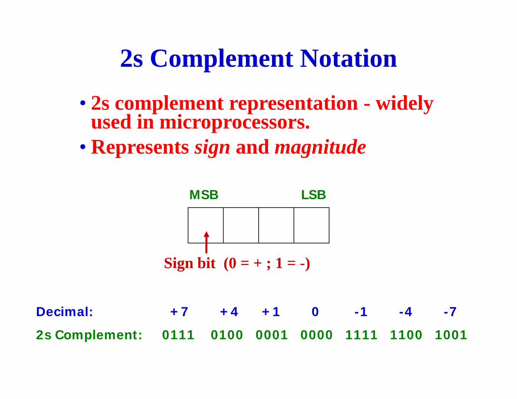
2s Complement Notation
• 2s complement representation - widely used in microprocessorsused in microprocessors.
• Represents sign and magnitude
MSB LSB
Sign bit (0 = + ; 1 = -)
Decimal: +7 +4 +1 0 -1 -4 -7
2s Complement: 0111 0100 0001 0000 1111 1100 1001
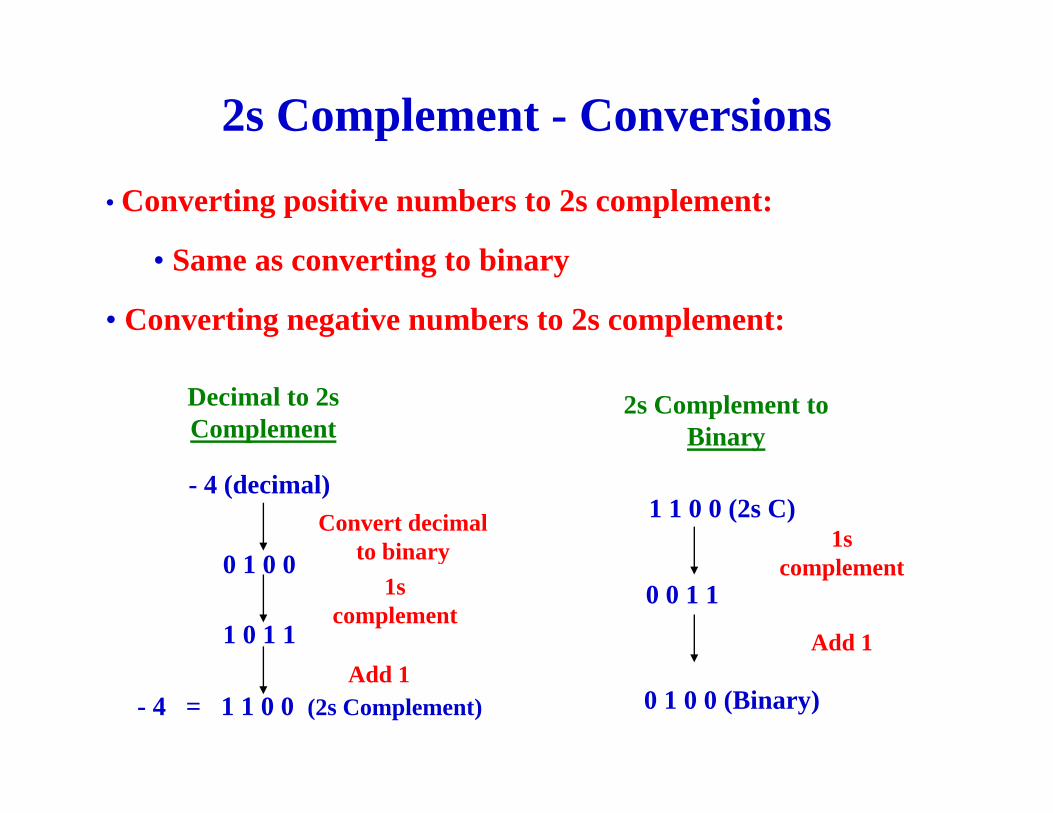
2s Complement - Conversions
• Converting positive numbers to 2s complement:
S ti t bi• Same as converting to binary
• Converting negative numbers to 2s complement:
Decimal to 2s Complement
2s Complement toBinary
- 4 (decimal)
0 1 0 0Convert decimal
to binary
1 1 0 0 (2s C)1s l t0 1 0 0
1 0 1 1
y1s
complement0 0 1 1
complement
Add 1
- 4 = 1 1 0 0 (2s Complement)Add 1
0 1 0 0 (Binary)
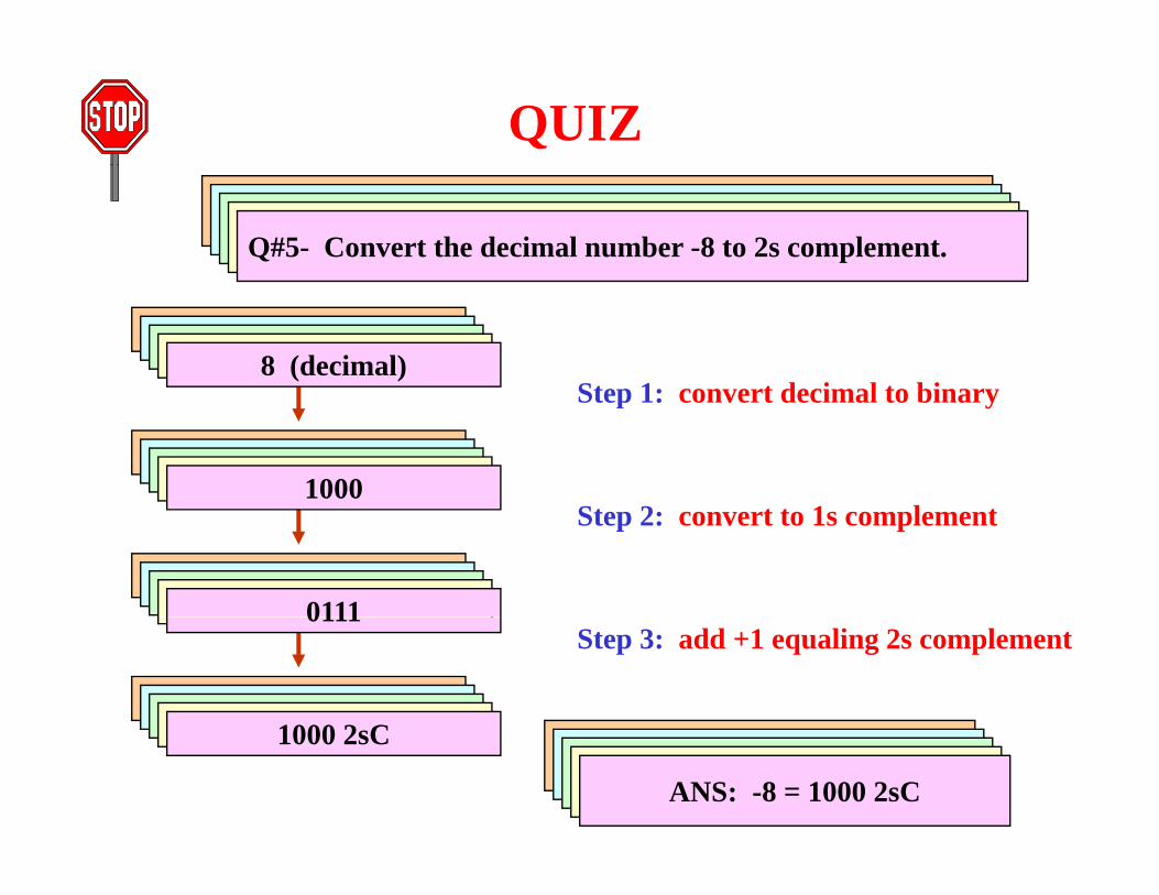
QUIZQ#1- Convert the decimal number –4 to 2s complement.Q#2- Convert the decimal number –-7 to 2s complement.Q#3- Convert the decimal number –1 to 2s complement.Q#4- Convert the decimal number +6 to 2s complement.Q#5- Convert the decimal number -8 to 2s complement.
4 (decimal)
Step 1: convert decimal to binary
7 (decimal)1 (decimal)6 (decimal)8 (decimal)
0100
Step 1: convert decimal to binary
0111000101101000
1011
Step 2: convert to 1s complement
10001110Not needed0111Step 3: add +1 equaling 2s complement
1100 2s C1001 2s C1111 2s CNot needed
0111
1000 2 CANS: -4 = 1100 2sCANS: -7 = 1001 2sCANS: -1 = 1111 2sC
Not needed
ANS: +6 = 0110 2sC
1000 2sC
ANS: -8 = 1000 2sC
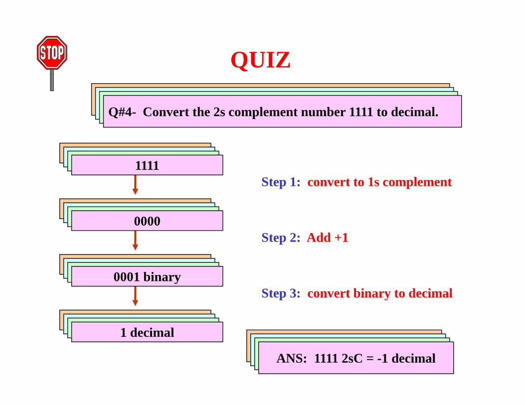
QUIZQ#1- Convert the 2s complement number 1110 to decimal.Q#2- Convert the 2s complement number 0101 to decimal.Q#3- Convert the 2s complement number 1001 to decimal.Q#4- Convert the 2s complement number 1111 to decimal.
1110Not needed10011111
0001
Step 1: convert to 1s complement
Not needed01100000
0010 binary
Step 2: Add +1
0101 binary0111 binary0001 binaryStep 3: convert binary to decimal
2 decimal5 decimal
y
7 decimal
0001 binary
1 d i lANS: 1110 2sC = -2 decimalANS: 0101 2sC = +5 decimal
7 decimal
ANS: 1001 2sC = -7 decimal
1 decimal
ANS: 1111 2sC = -1 decimal
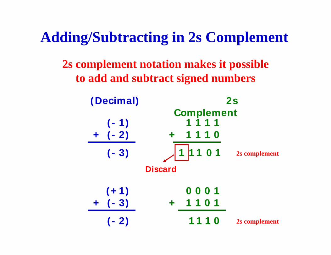
Adding/Subtracting in 2s Complement
2s complement notation makes it possible to add and subtract signed numbersto add and subtract signed numbers
(Decimal) 2s Complement
(- 1)+ (- 2)
1 1 1 1+ 1 1 1 0
Complement
(- 3) 10111
Discard
2s complement
(+1)+ (- 3)
0 0 0 1+ 1 1 0 1( )
(- 2) 0111 2s complement
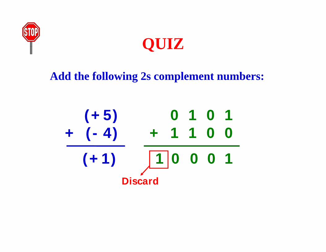
QUIZ
Add the following 2s complement numbers:
QUIZ
Add the following 2s complement numbers:
0 1 0 1( 5) 0 1 0 1+ 1 1 0 0
(+5)+ (- 4)
10001(+1)Discard
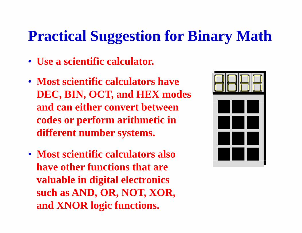
Practical Suggestion for Binary Mathgg y• Use a scientific calculator.
• Most scientific calculators have DEC, BIN, OCT, and HEX modes and can either convert between codes or perform arithmetic in different number systemsdifferent number systems.
• Most scientific calculators also have other functions that are valuable in digital electronics
h AND OR NOT XORsuch as AND, OR, NOT, XOR, and XNOR logic functions.
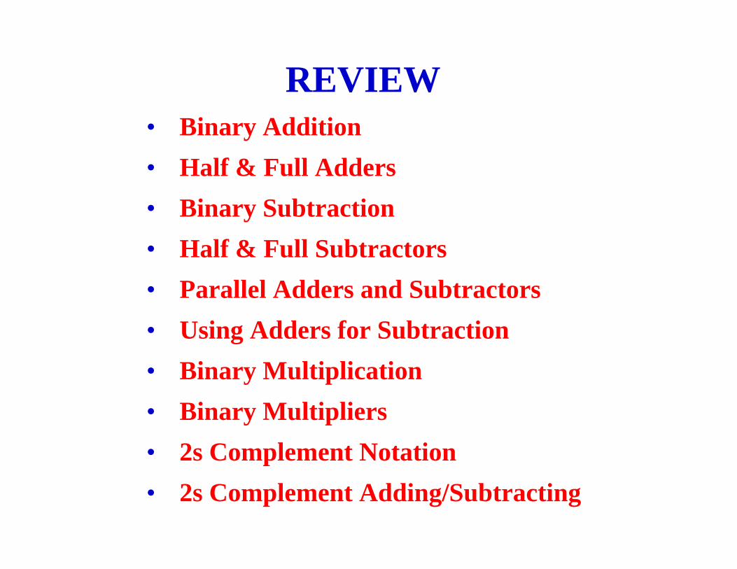
REVIEW• Binary Addition• Half & Full Adders• Binary Subtraction• Half & Full Subtractors• Half & Full Subtractors• Parallel Adders and Subtractors• Using Adders for Subtraction• Binary Multiplication• Binary Multipliers• 2s Complement Notationp• 2s Complement Adding/Subtracting
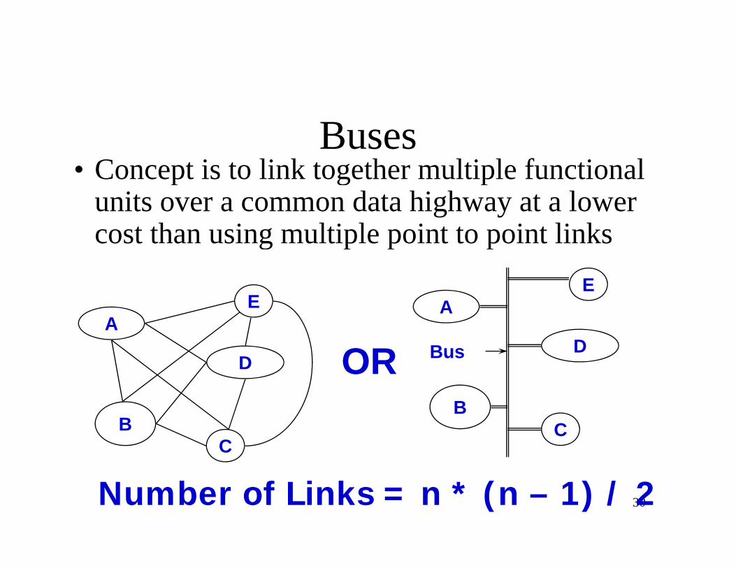
Buses• Concept is to link together multiple functionalConcept is to link together multiple functional
units over a common data highway at a lower cost than using multiple point to point linksg p p p
AE
AE
DBusA
D ORB
CBC
30Number of Links = n * (n – 1) / 2
Bus - Essential Part of Any Computer
CPU PrimaryMemory
SecondaryMemory
I/OMemory Memory
DataData
Address
Control
31
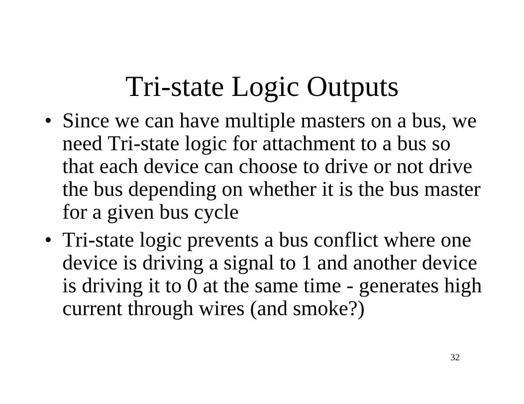
Tri-state Logic Outputs• Since we can have multiple masters on a bus, weSince we can have multiple masters on a bus, we
need Tri-state logic for attachment to a bus so that each device can choose to drive or not drive the bus depending on whether it is the bus master for a given bus cycle
• Tri-state logic prevents a bus conflict where one device is driving a signal to 1 and another device i d i i i 0 h i hi his driving it to 0 at the same time - generates high current through wires (and smoke?)
32
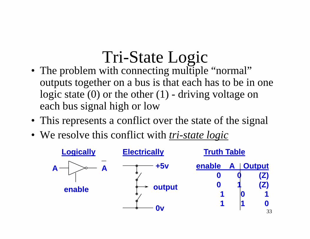
Tri-State Logic• The problem with connecting multiple “normal” p g p
outputs together on a bus is that each has to be in one logic state (0) or the other (1) - driving voltage on each b s signal high or loeach bus signal high or low
• This represents a conflict over the state of the signal• We resolve this conflict with tri state logic• We resolve this conflict with tri-state logic
+5v
Logically Electrically Truth Table
enable A Output+5v
output
A A
enable
enable A Output0 0 (Z)0 1 (Z)1 0 1
330v
1 0 11 1 0
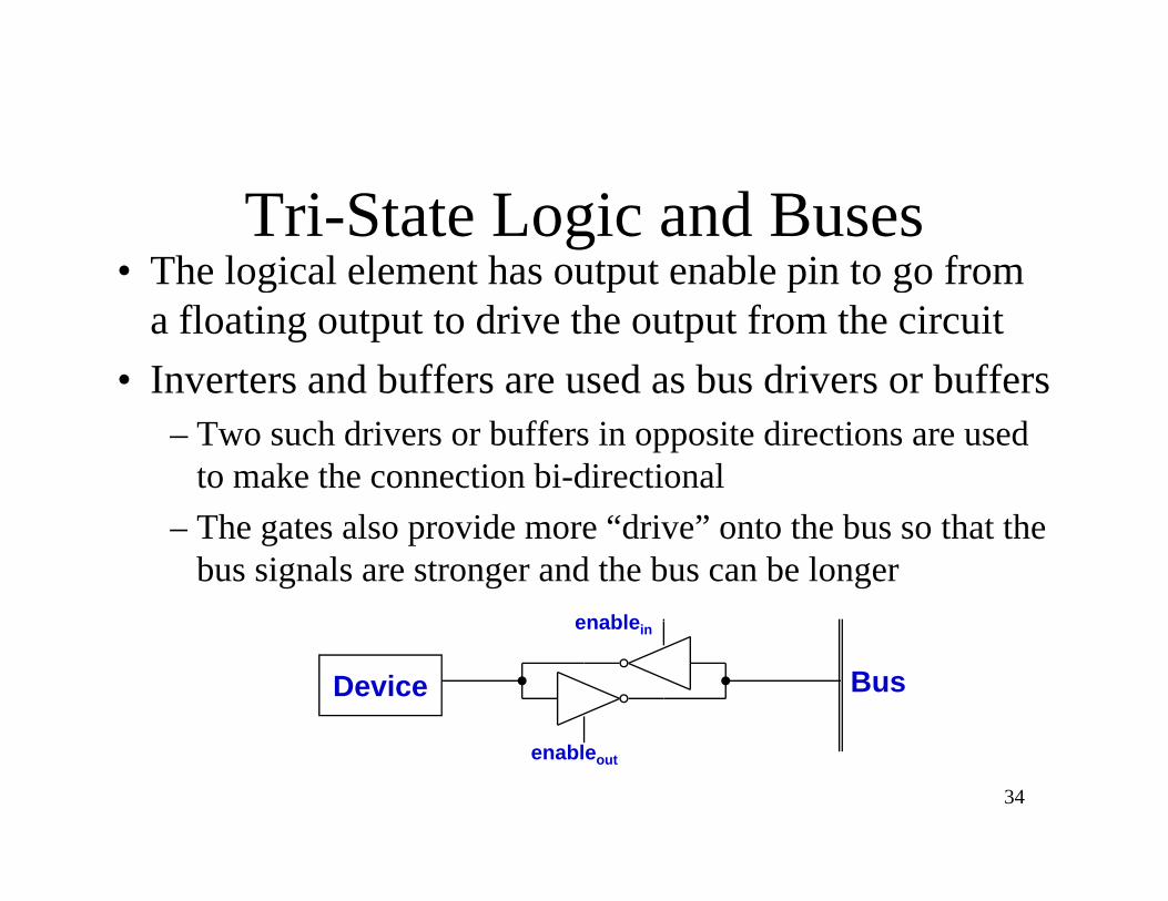
Tri-State Logic and Buses• The logical element has output enable pin to go fromThe logical element has output enable pin to go from
a floating output to drive the output from the circuit• Inverters and buffers are used as bus drivers or buffers
– Two such drivers or buffers in opposite directions are used to make the connection bi-directional
– The gates also provide more “drive” onto the bus so that the bus signals are stronger and the bus can be longer
enableenablein
Device Bus
34
enableout
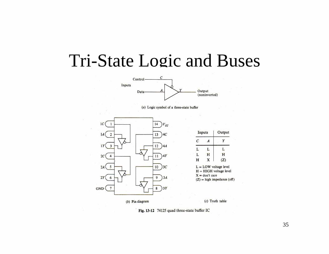
Tri-State Logic and Buses
35
Bus Master – Slave Relationships• During any specific bus cycle, only one deviceDuring any specific bus cycle, only one device
attached to the bus is allowed to drive it• Driving the bus means that a device is forcingDriving the bus means that a device is forcing
each signal on the bus to a high or low state• For the data bus, the processor, a memory chip,For the data bus, the processor, a memory chip,
or an I/O device may be driving the data bus during a specific read or write bus cycleg p y
• Specific signals on the address and control bus select a device to be the master on the data bus
36
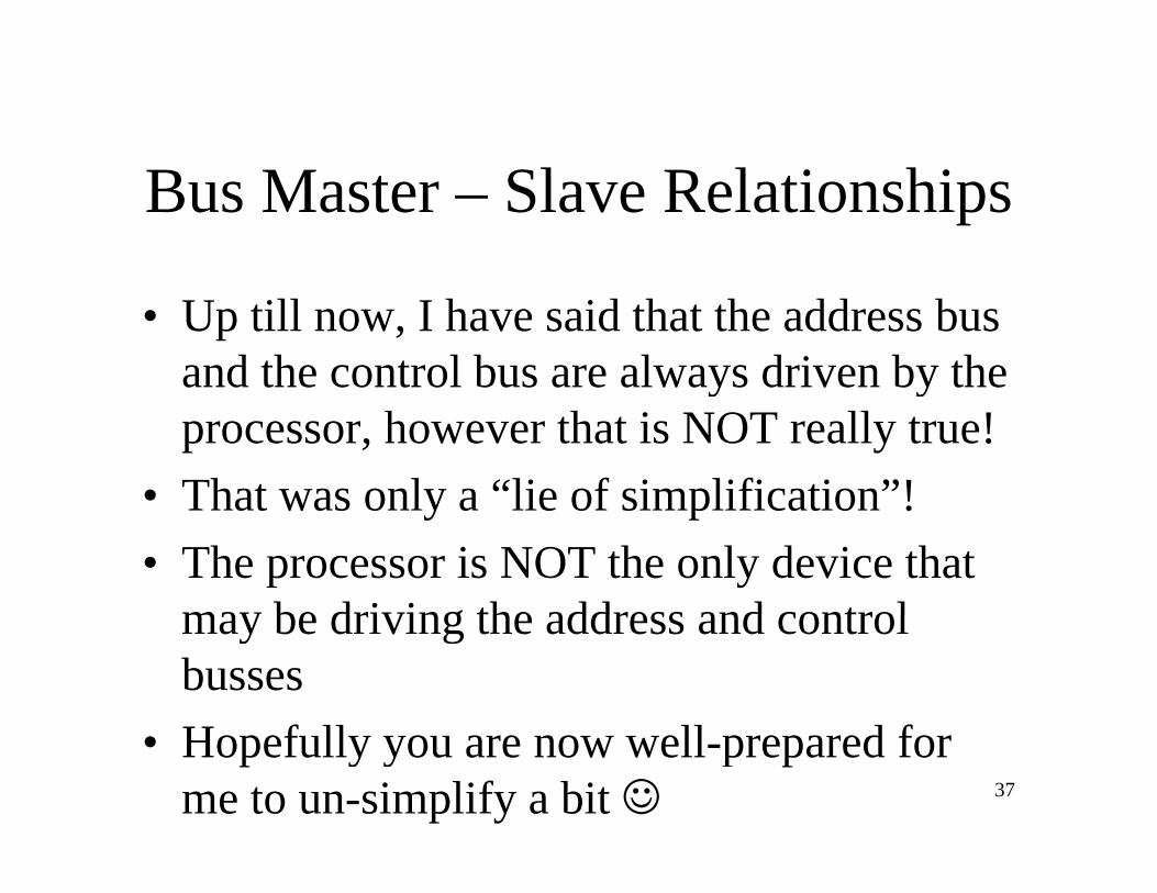
Bus Master – Slave Relationships
• Up till now, I have said that the address bus and the control bus are always driven by the y yprocessor, however that is NOT really true!
• That was only a “lie of simplification”!That was only a lie of simplification !• The processor is NOT the only device that
may be driving the address and controlmay be driving the address and control busses H f ll ll d f
37
• Hopefully you are now well-prepared for me to un-simplify a bit ☺
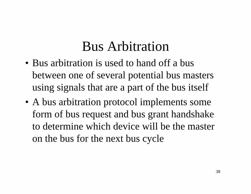
Bus ArbitrationB bit ti i d t h d ff b• Bus arbitration is used to hand off a bus between one of several potential bus masters
i i l th t t f th b it lfusing signals that are a part of the bus itself• A bus arbitration protocol implements some
form of bus request and bus grant handshake to determine which device will be the master on the bus for the next bus cycle
38
Bus Master – Slave Relationships
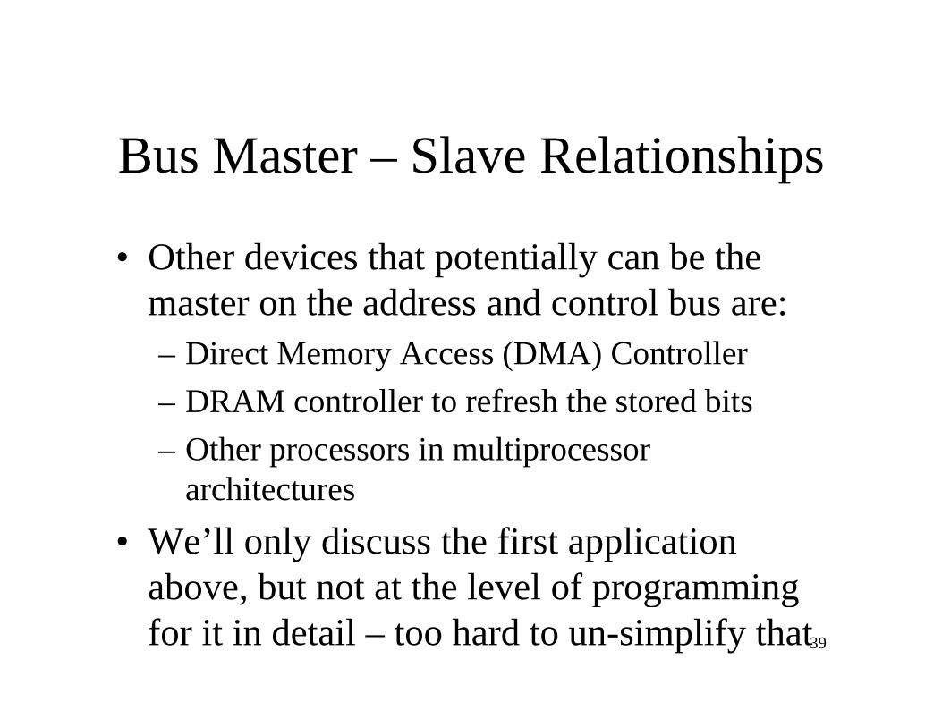
• Other devices that potentially can be the master on the address and control bus are:– Direct Memory Access (DMA) Controller– DRAM controller to refresh the stored bitsDRAM controller to refresh the stored bits– Other processors in multiprocessor
architectures• We’ll only discuss the first application
above but not at the level of programming39
above, but not at the level of programming for it in detail – too hard to un-simplify that
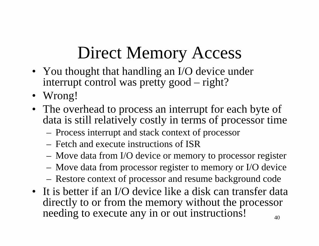
Direct Memory Access• You thought that handling an I/O device under g g
interrupt control was pretty good – right? • Wrong!
The o erhead to process an interr pt for each b te of• The overhead to process an interrupt for each byte of data is still relatively costly in terms of processor time– Process interrupt and stack context of processor– Fetch and execute instructions of ISR– Move data from I/O device or memory to processor register– Move data from processor register to memory or I/O deviceMove data from processor register to memory or I/O device– Restore context of processor and resume background code
• It is better if an I/O device like a disk can transfer data directl to or from the memor itho t the processor
40
directly to or from the memory without the processor needing to execute any in or out instructions!
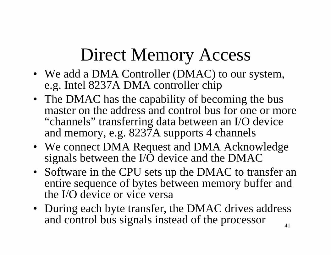
Direct Memory Access• We add a DMA Controller (DMAC) to our system, ( ) y ,
e.g. Intel 8237A DMA controller chip • The DMAC has the capability of becoming the bus
master on the address and control bus for one or moremaster on the address and control bus for one or more “channels” transferring data between an I/O device and memory, e.g. 8237A supports 4 channelsW t DMA R t d DMA A k l d• We connect DMA Request and DMA Acknowledge signals between the I/O device and the DMAC
• Software in the CPU sets up the DMAC to transfer an So w e e C U se s up e C o s eentire sequence of bytes between memory buffer and the I/O device or vice versa
• During each byte transfer the DMAC drives address41
• During each byte transfer, the DMAC drives address and control bus signals instead of the processor
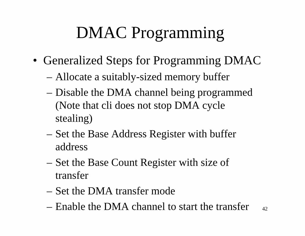
DMAC Programming• Generalized Steps for Programming DMAC
All i bl i d b ff– Allocate a suitably-sized memory buffer– Disable the DMA channel being programmed
(N t th t li d t t DMA l(Note that cli does not stop DMA cycle stealing)Set the Base Address Register with buffer– Set the Base Address Register with buffer addressSet the Base Count Register with size of– Set the Base Count Register with size of transfer
– Set the DMA transfer mode42
Set the DMA transfer mode– Enable the DMA channel to start the transfer
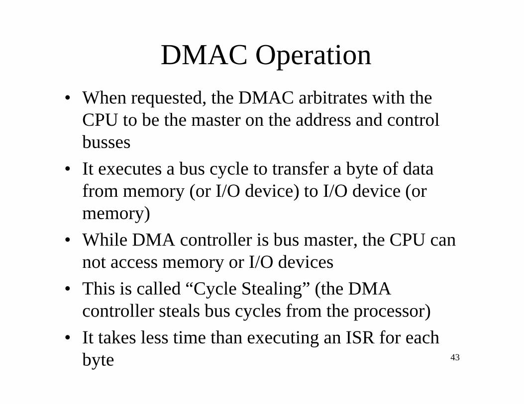
DMAC Operation• When requested, the DMAC arbitrates with the
CPU to be the master on the address and controlCPU to be the master on the address and control busses
• It executes a bus cycle to transfer a byte of data y yfrom memory (or I/O device) to I/O device (or memory)
• While DMA controller is bus master, the CPU can not access memory or I/O devices
• This is called “Cycle Stealing” (the DMA controller steals bus cycles from the processor)
43
• It takes less time than executing an ISR for each byte
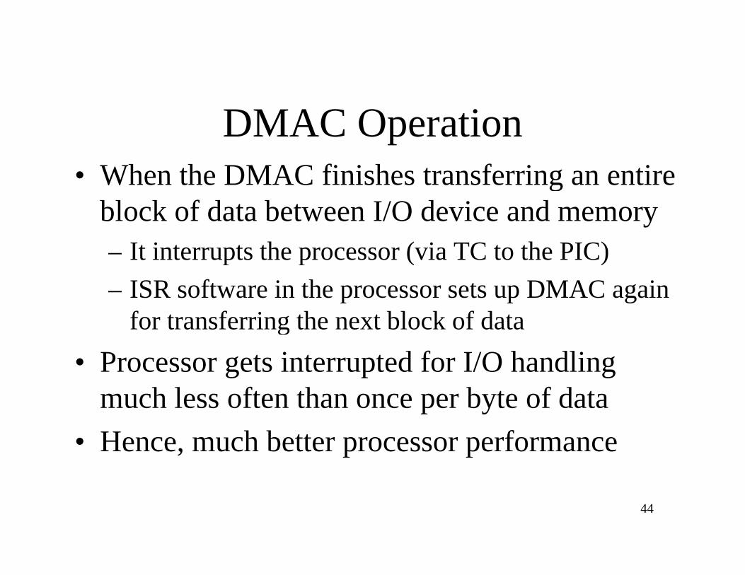
DMAC Operation• When the DMAC finishes transferring an entireWhen the DMAC finishes transferring an entire
block of data between I/O device and memory It interrupts the processor (via TC to the PIC)– It interrupts the processor (via TC to the PIC)
– ISR software in the processor sets up DMAC again for transferring the next block of datafor transferring the next block of data
• Processor gets interrupted for I/O handling much less often than once per byte of datamuch less often than once per byte of data
• Hence, much better processor performance
44
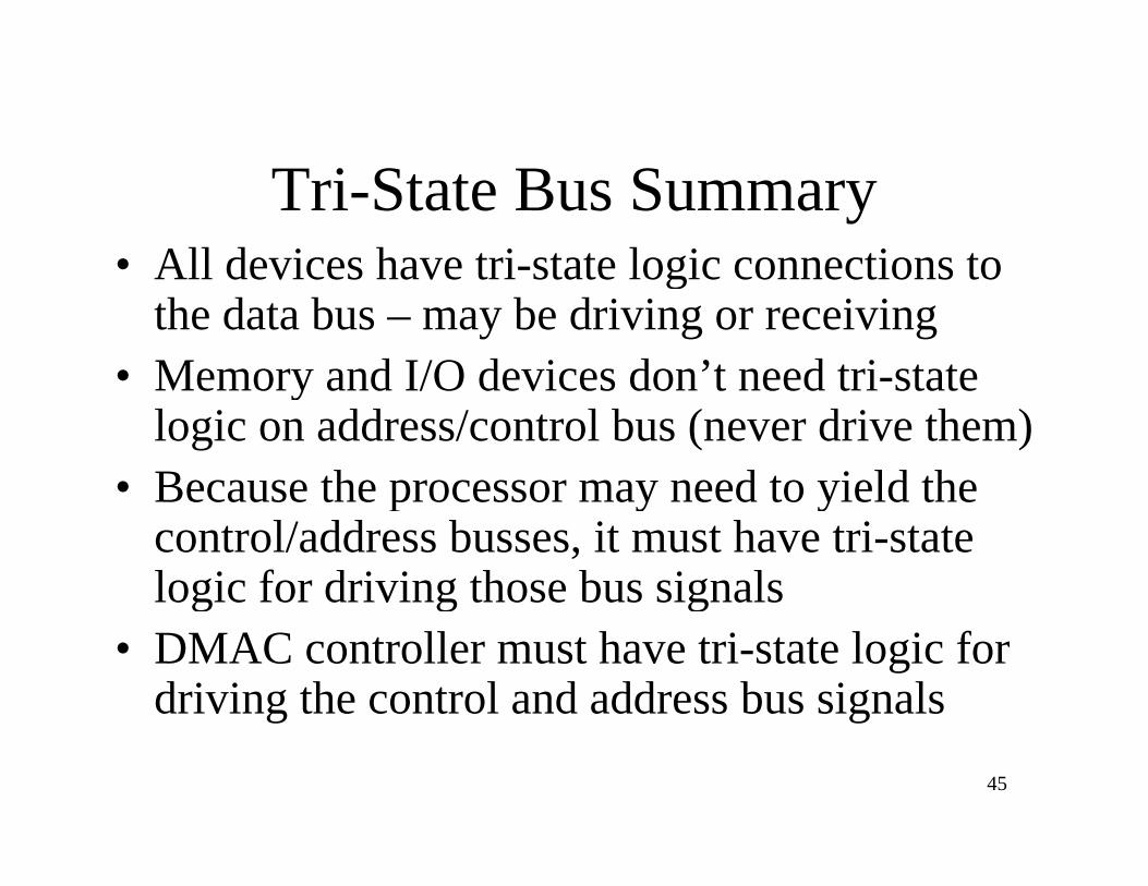
Tri-State Bus Summary• All devices have tri-state logic connections toAll devices have tri state logic connections to
the data bus – may be driving or receiving• Memory and I/O devices don’t need tri-stateMemory and I/O devices don t need tri state
logic on address/control bus (never drive them)• Because the processor may need to yield theBecause the processor may need to yield the
control/address busses, it must have tri-state logic for driving those bus signalsg g g
• DMAC controller must have tri-state logic for driving the control and address bus signals
45
g g
Propagation & Transmission delayp g y
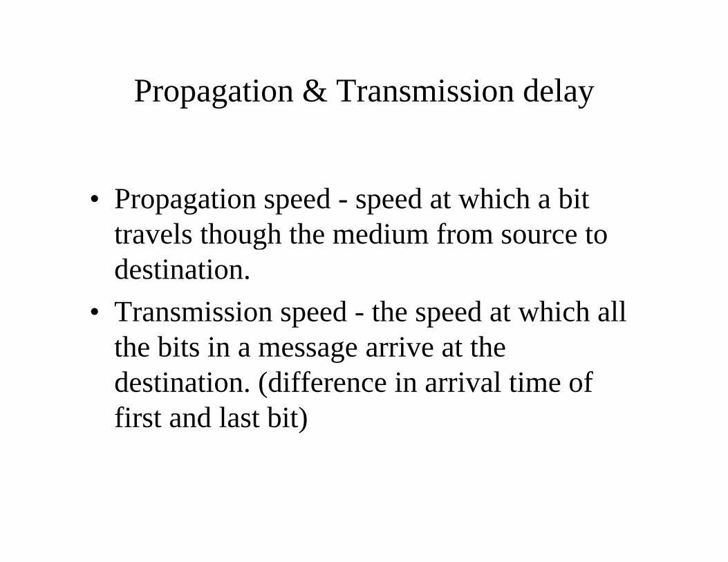
• Propagation speed - speed at which a bit travels though the medium from source to gdestination.
• Transmission speed - the speed at which allTransmission speed the speed at which all the bits in a message arrive at the destination (difference in arrival time ofdestination. (difference in arrival time of first and last bit)
Propagation and Transmission DelayPropagation and Transmission Delay
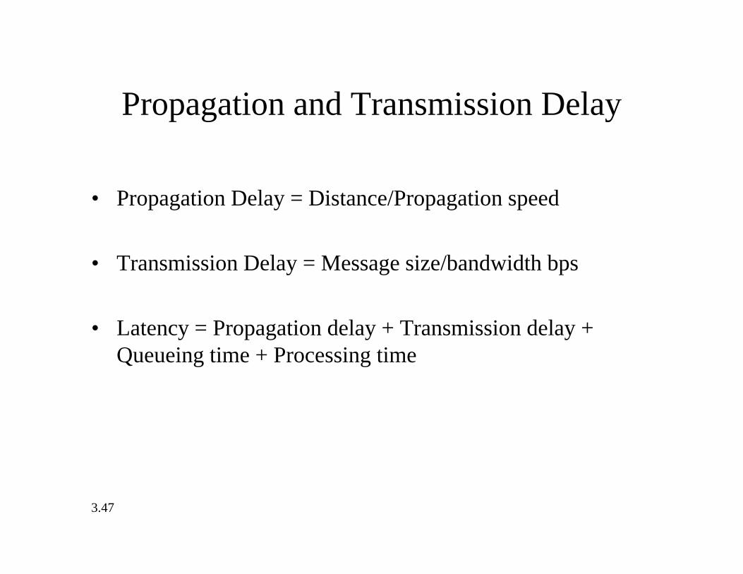
• Propagation Delay = Distance/Propagation speed
• Transmission Delay = Message size/bandwidth bps
L t P ti d l + T i i d l +• Latency = Propagation delay + Transmission delay + Queueing time + Processing time
3.47
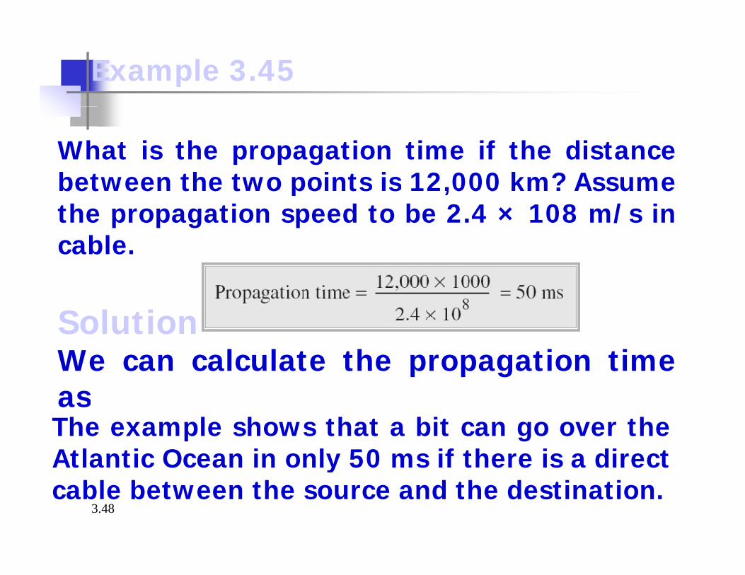
Example 3.45
What is the propagation time if the distancebetween the two points is 12 000 km? Assumebetween the two points is 12,000 km? Assumethe propagation speed to be 2.4 × 10⁸ m/s incable.cable.
SolutionSolutionWe can calculate the propagation timeasasThe example shows that a bit can go over theAtlantic Ocean in only 50 ms if there is a direct
3.48
ycable between the source and the destination.
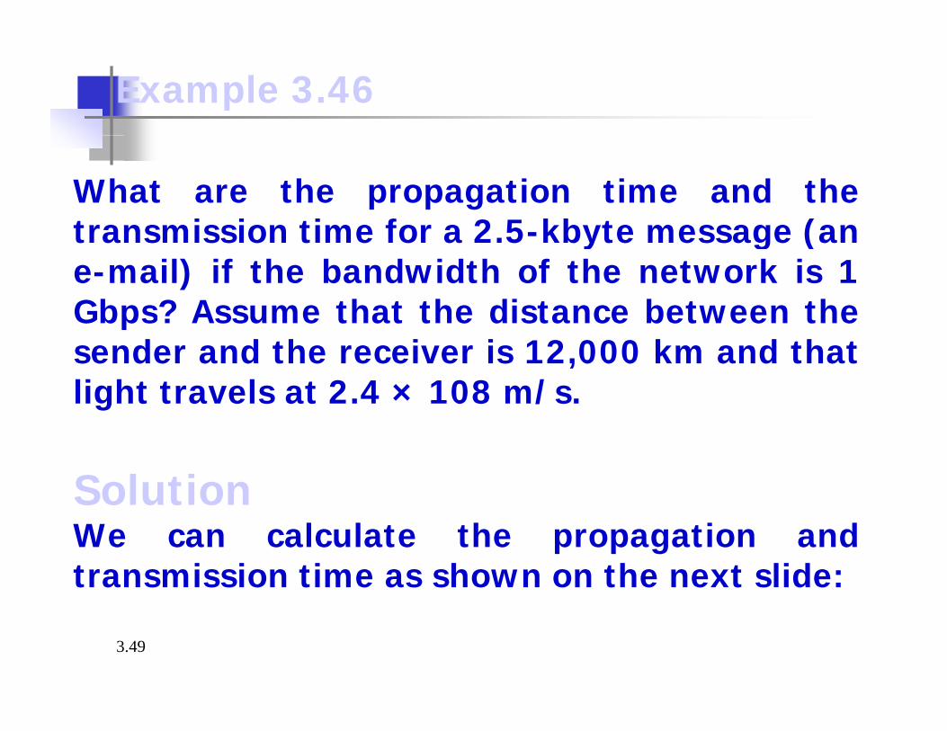
Example 3.46
What are the propagation time and thetransmission time for a 2 5 kbyte message (antransmission time for a 2.5-kbyte message (ane-mail) if the bandwidth of the network is 1Gbps? Assume that the distance between theGbps? Assume that the distance between thesender and the receiver is 12,000 km and thatlight travels at 2.4 × 10⁸ m/s.
SolutionSolutionWe can calculate the propagation andtransmission time as shown on the next slide:
3.49
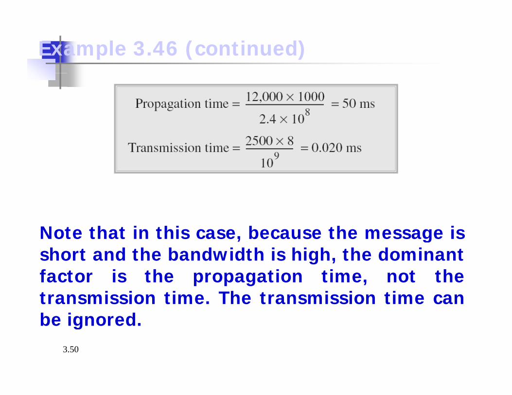
Example 3.46 (continued)
Note that in this case, because the message isshort and the bandwidth is high, the dominantfacto is the p opagation time not thefactor is the propagation time, not thetransmission time. The transmission time canbe ignored
3.50
be ignored.
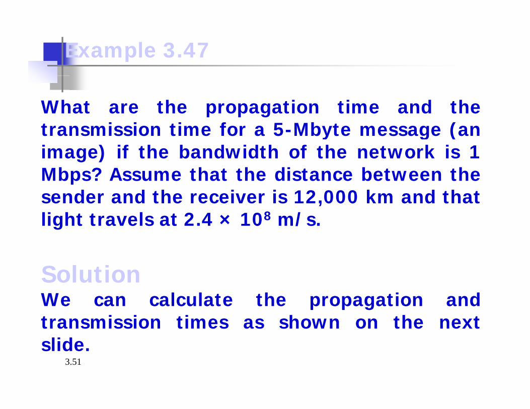
Example 3.47
What are the propagation time and thetransmission time for a 5 Mbyte message (antransmission time for a 5-Mbyte message (animage) if the bandwidth of the network is 1Mbps? Assume that the distance between theMbps? Assume that the distance between thesender and the receiver is 12,000 km and thatlight travels at 2.4 × 10⁸ m/s.
SolutionSolutionWe can calculate the propagation andtransmission times as shown on the next
3.51slide.
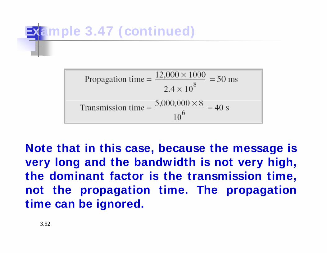
Example 3.47 (continued)
Note that in this case, because the message isvery long and the bandwidth is not very high,the dominant factor is the transmission timethe dominant factor is the transmission time,not the propagation time. The propagationtime can be ignored.
3.52
time can be ignored.
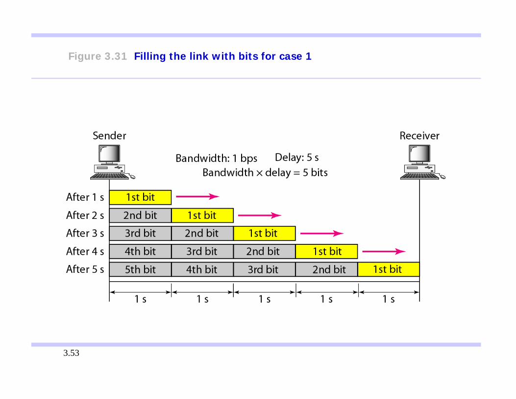
Figure 3.31 Filling the link with bits for case 1
3.53
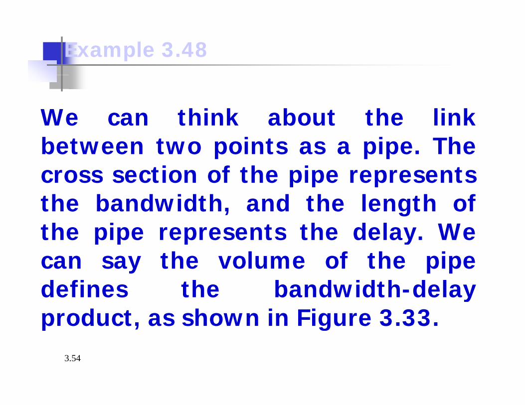
Example 3.48
We can think about the linkbetween two points as a pipe. Thecross section of the pipe representscross section of the pipe representsthe bandwidth, and the length ofthe pipe represents the delay Wethe pipe represents the delay. Wecan say the volume of the piped fi h b d id h d ldefines the bandwidth-delayproduct, as shown in Figure 3.33.
3.54
p g
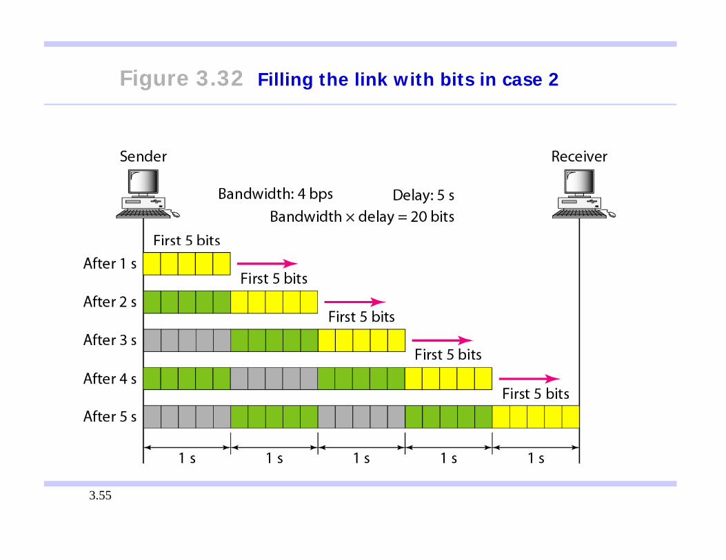
Figure 3.32 Filling the link with bits in case 2
3.55
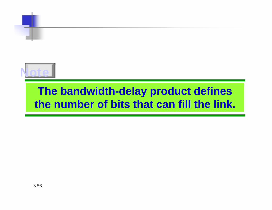
The bandwidth-delay product definesNote
The bandwidth-delay product defines the number of bits that can fill the link.
3.56
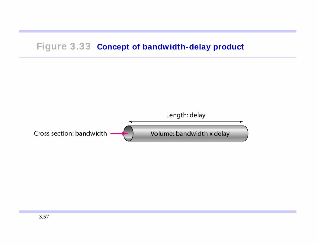
Figure 3 33 Concept of bandwidth delay productFigure 3.33 Concept of bandwidth-delay product
3.57
![Communication Skills [CMS] - Vidyalankarvidyalankar.org/file/diploma/SemII/civil.pdf · Communication Skills [CMS] ... (Dass H.K.) S. Chand Publication – New Delhi. 4. Fundamentals](https://img.pdfslide.us/doc/110x75/5af11ea07f8b9abc788e0911/communication-skills-cms-vi-skills-cms-dass-hk-s-chand-publication.jpg)


![Communication Skills [CMS] - Vidyalankarvidyalankar.org/file/diploma/SemII/mech.pdf · Communication Skills [CMS] ... SYLLABUS Topic 1 Complex number ... A text book of engineering](https://img.pdfslide.us/doc/110x75/5a701e737f8b9aac538ba56a/communication-skills-cms-vidyalankarvidyalankarorgfilediplomasemiimechpdfpdf.jpg)


![Communication Skills [CMS] - Vidyalankarvidyalankar.org/file/diploma/SemII/Etrx.pdf · Communication Skills [CMS] ... circuit diagram, process of photoelectric emission, definitions:-](https://img.pdfslide.us/doc/110x75/5af772cf7f8b9aac248bdc4b/communication-skills-cms-vi-skills-cms-circuit-diagram-process-of-photoelectric.jpg)
![Communication Skills [CMS] - Vidyalankar Coaching …vidyalankar.org/file/diploma/SemII/elec.pdf · Communication Skills [CMS] F.Y. Diploma : Sem. II ... law of moments Varignon’s](https://img.pdfslide.us/doc/110x75/5ae6bbeb7f8b9a8b2b8da6c9/communication-skills-cms-vidyalankar-coaching-skills-cms-fy-diploma.jpg)