Embed Size (px)
Citation preview
MOS LayerMOS Layer
MOS LayerMOS Layer
• MOS design is aimed at turning a specificationMOS design is aimed at turning a specification into masks for processing silicon to meet the specificationspecification.
• We have seen that MOS circuits are formed on four basic layers n diffusion p diffusiqnfour basic layers‐n‐diffusion, p‐diffusiqn, polysilicon, and metal, which are isolated from one another by thick or thin (thinox) siliconone another by thick or thin (thinox) silicon dioxide insulating layers.
Mask Layout (Print this presentation in colour if possible, otherwise highlight colours)
• Circuit coloured mask layer layout
C l d i k di k i• Coloured stick diagram mask representation
• Lambda and layout design rules
• Mask layout of nMOS and CMOS inverters
• Mask layout of CMOS circuits (examples)Mask layout of CMOS circuits (examples)
• Reading & understanding mask layout (exercises)
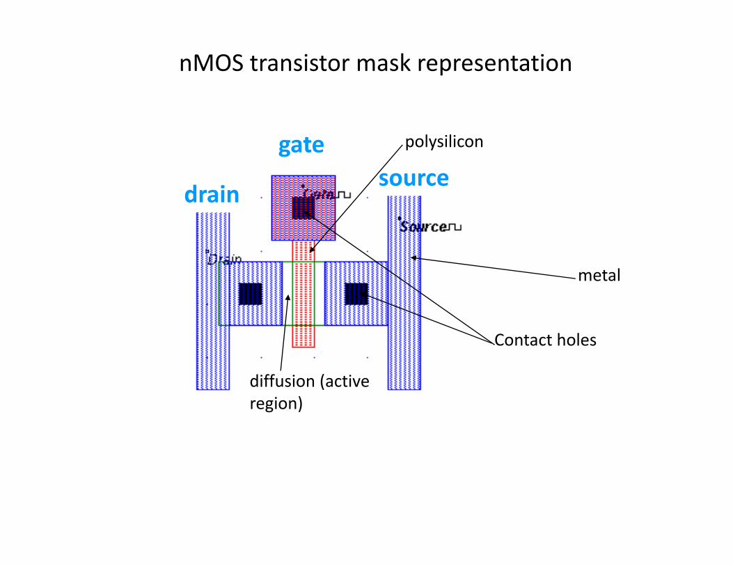
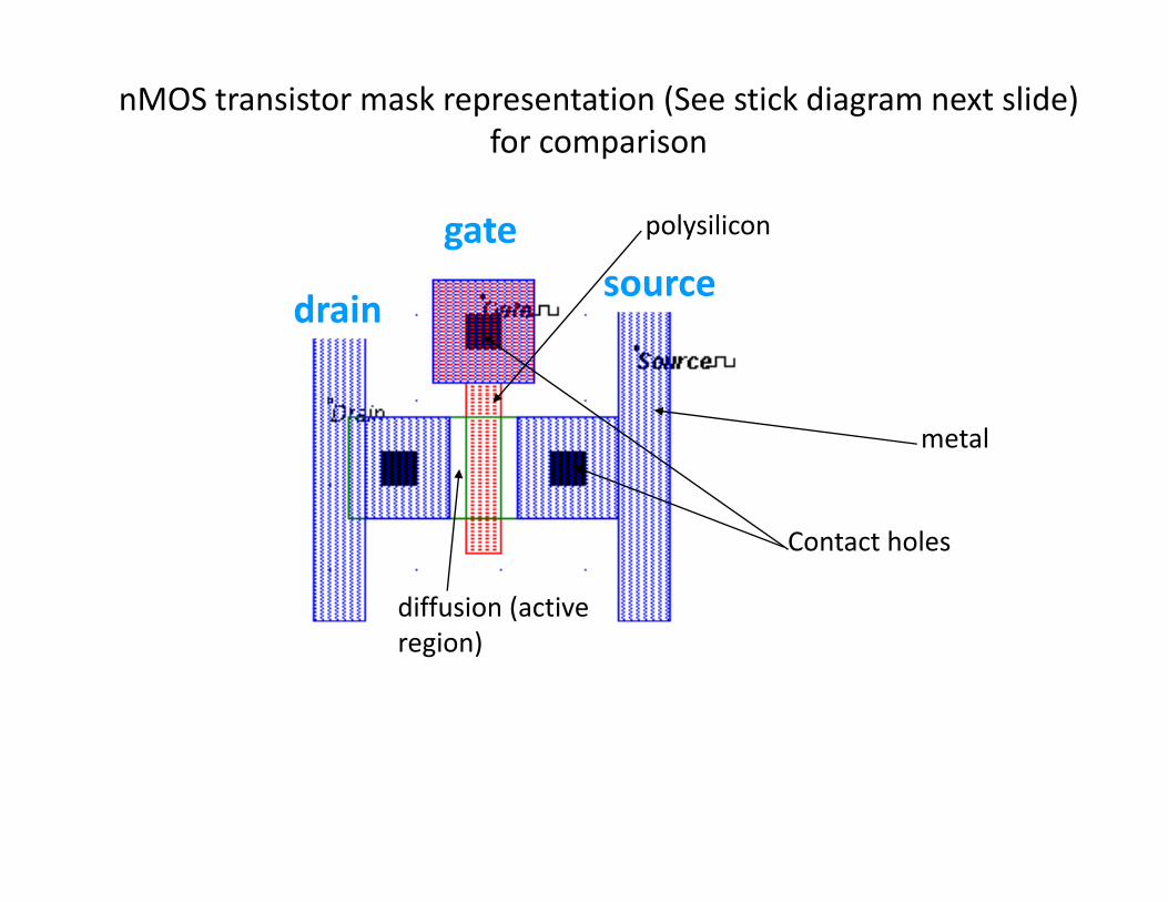
nMOS transistor mask representation
gatesource
polysilicon
drainsource
metal
Contact holes
diffusion (activeregion)
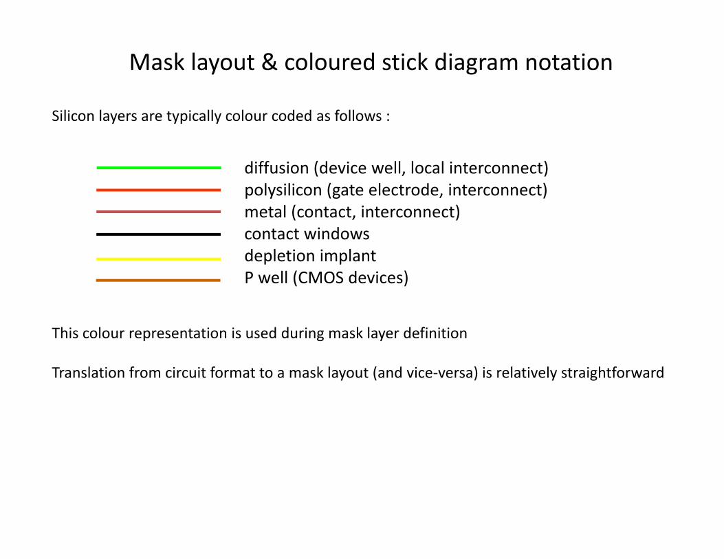
Mask layout & coloured stick diagram notation
Silicon layers are typically colour coded as follows :
diffusion (device well, local interconnect)( , )polysilicon (gate electrode, interconnect)metal (contact, interconnect)contact windowsdepletion implantP well (CMOS devices)
This colour representation is used during mask layer definition
Translation from circuit format to a mask layout (and vice‐versa) is relatively straightforward
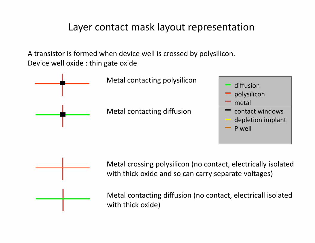
Layer contact mask layout representation
A transistor is formed when device well is crossed by polysilicon. Device well oxide : thin gate oxide
Metal contacting polysilicondiffusionpolysilicon metal
Metal contacting diffusion contact windowsdepletion implantP well
Metal crossing polysilicon (no contact, electrically isolated
Metal contacting diffusion (no contact, electricall isolated
g p y ( , ywith thick oxide and so can carry separate voltages)
g ( ,with thick oxide)
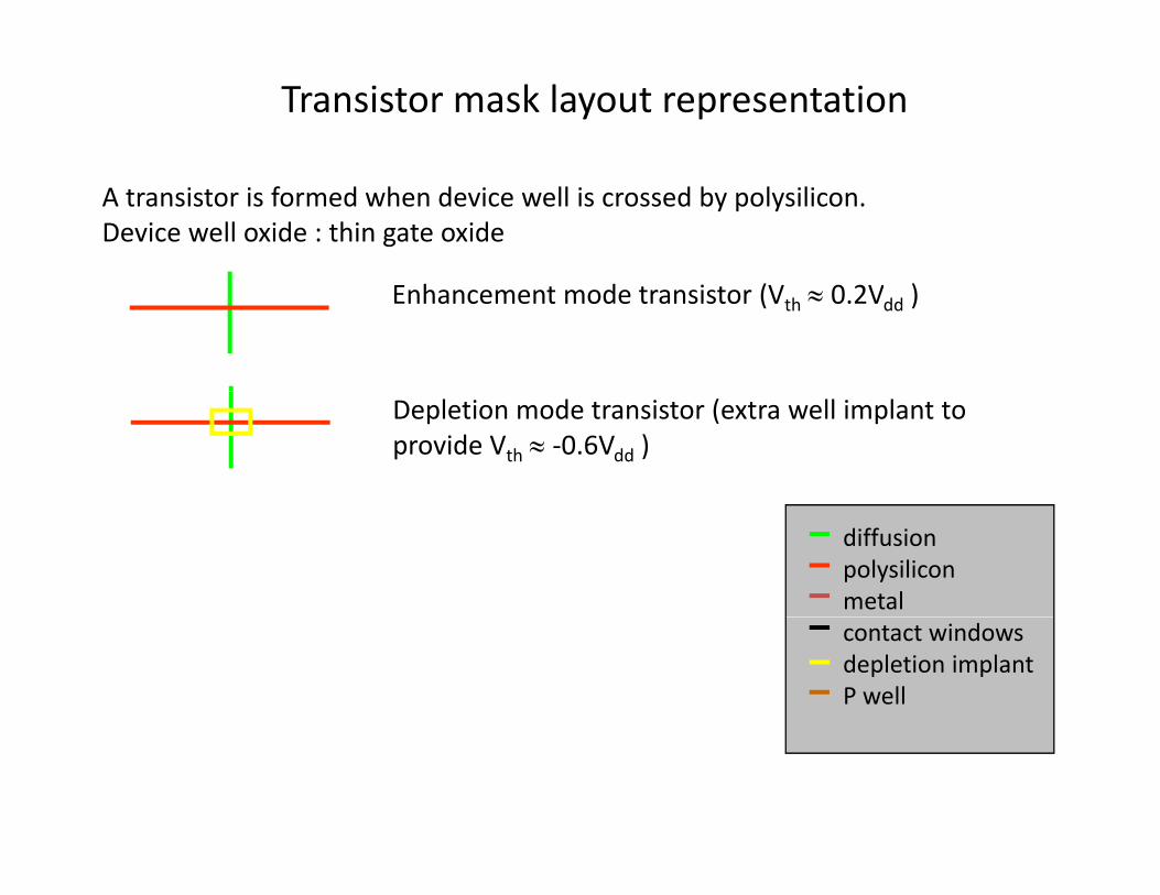
Transistor mask layout representation
A transistor is formed when device well is crossed by polysilicon. Device well oxide : thin gate oxide
Enhancement mode transistor (Vth ≈ 0.2Vdd )
Depletion mode transistor (extra well implant to provide Vth ≈ ‐0.6Vdd )
diffusionpolysilicon metal contact windowsdepletion implantP well
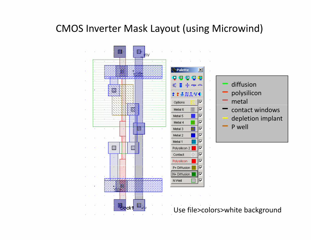
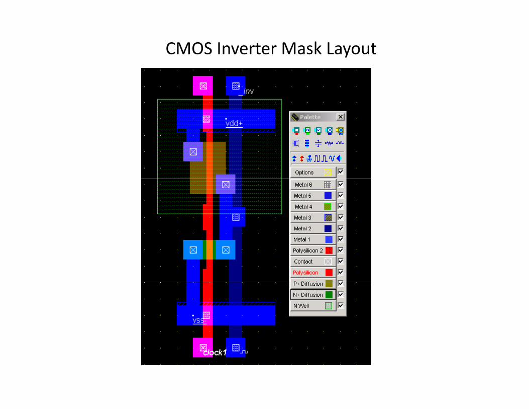
CMOS Inverter Mask Layout (using Microwind)
diffusionpolysilicon metal contact windowsdepletion implantP well
Use file>colors>white background
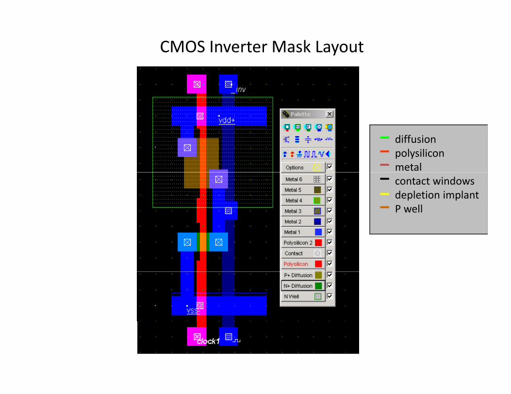
CMOS Inverter Mask Layout
diffusionpolysilicon metal contact windowsdepletion implantP well
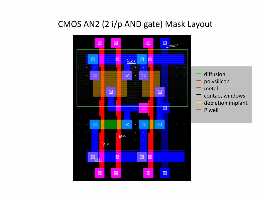
CMOS AN2 (2 i/p AND gate) Mask Layout
diffusionpolysilicon metalmetal contact windowsdepletion implantP well
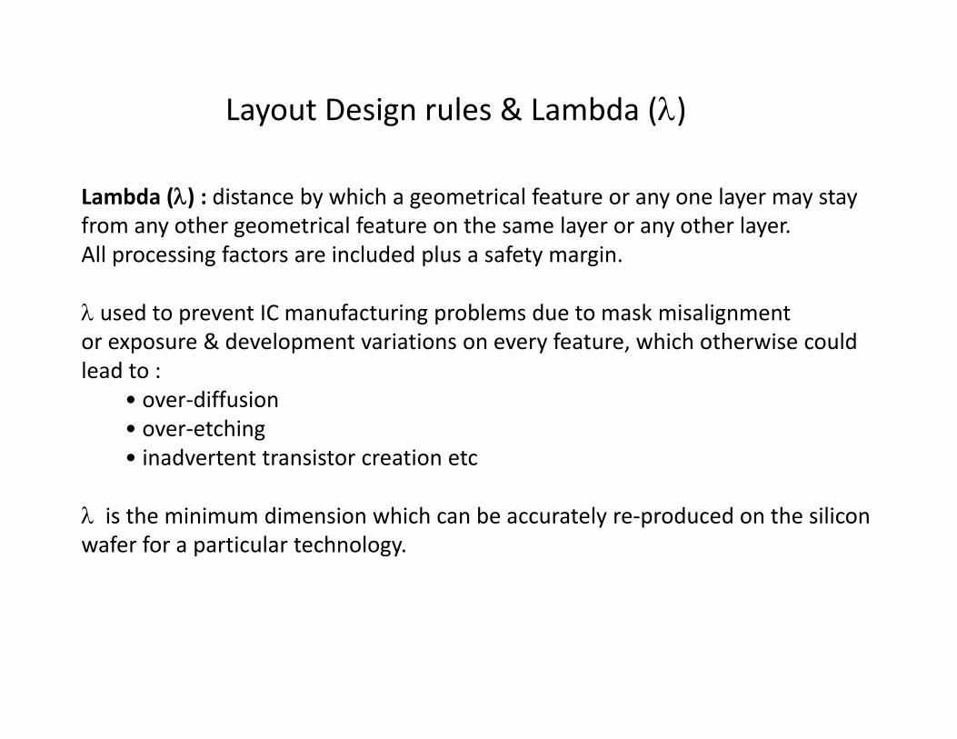
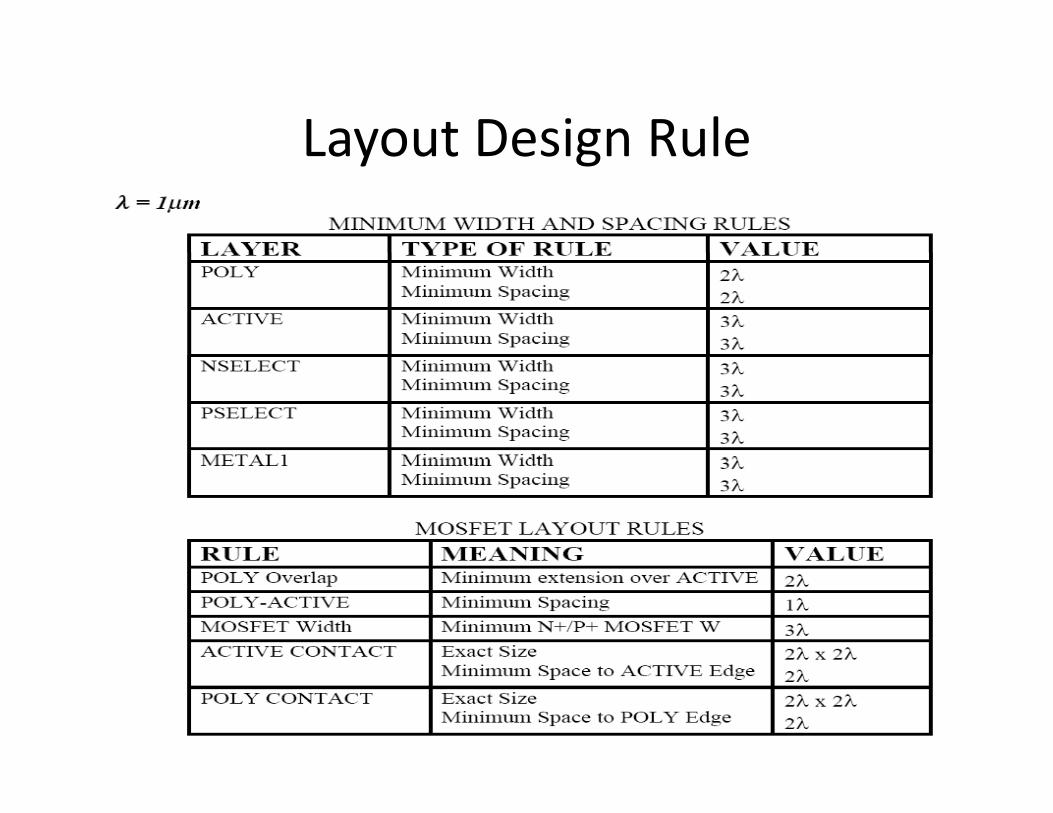
Layout Design rules & Lambda (λ)
Lambda (λ) : distance by which a geometrical feature or any one layer may stay from any other geometrical feature on the same layer or any other layerfrom any other geometrical feature on the same layer or any other layer. All processing factors are included plus a safety margin.
λ used to prevent IC manufacturing problems due to mask misalignment p g p gor exposure & development variations on every feature, which otherwise could lead to :
• over‐diffusion• over‐etching• inadvertent transistor creation etc
λ i th i i di i hi h b t l d d th iliλ is the minimum dimension which can be accurately re‐produced on the silicon wafer for a particular technology.
Layout Design rules & Lambda (λ)
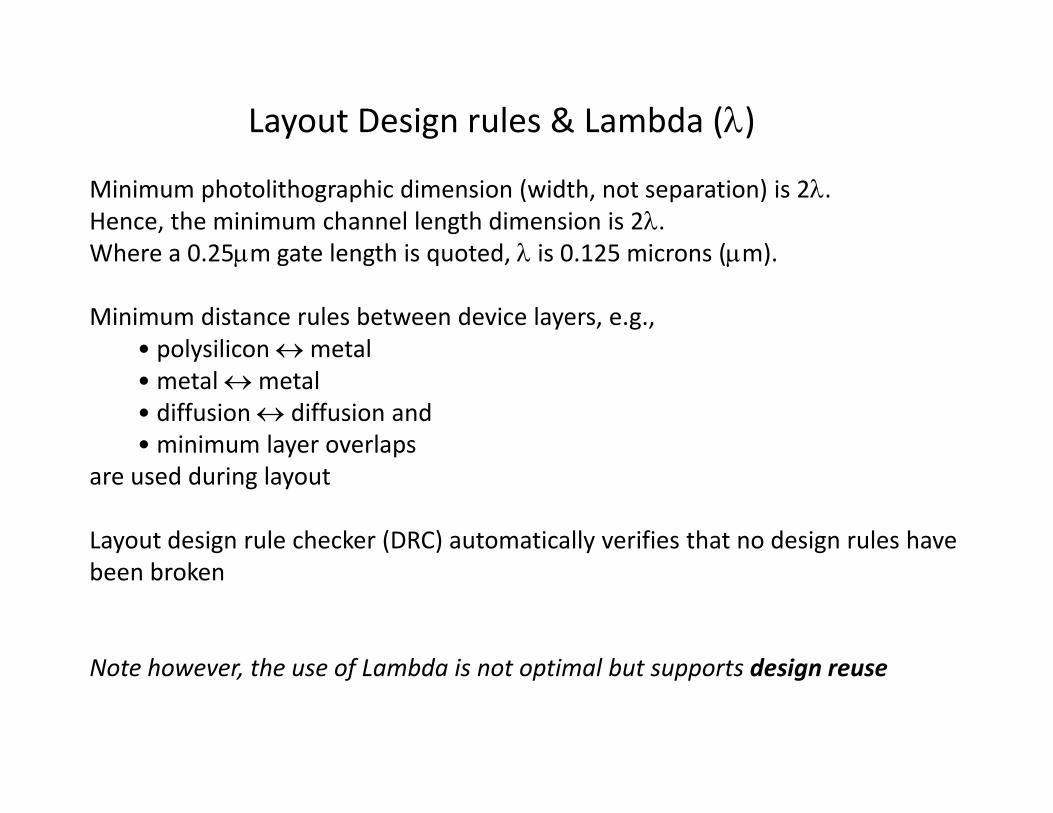
Minimum photolithographic dimension (width, not separation) is 2λ. Hence, the minimum channel length dimension is 2λ. Where a 0 25μm gate length is quoted λ is 0 125 microns (μm)Where a 0.25μm gate length is quoted, λ is 0.125 microns (μm).
Minimum distance rules between device layers, e.g., • polysilicon↔metalpolysilicon ↔metal • metal ↔metal• diffusion ↔ diffusion and • minimum layer overlaps
are used during layout
Layout design rule checker (DRC) automatically verifies that no design rules have been broken
N t h th f L bd i t ti l b t t d iNote however, the use of Lambda is not optimal but supports design reuse
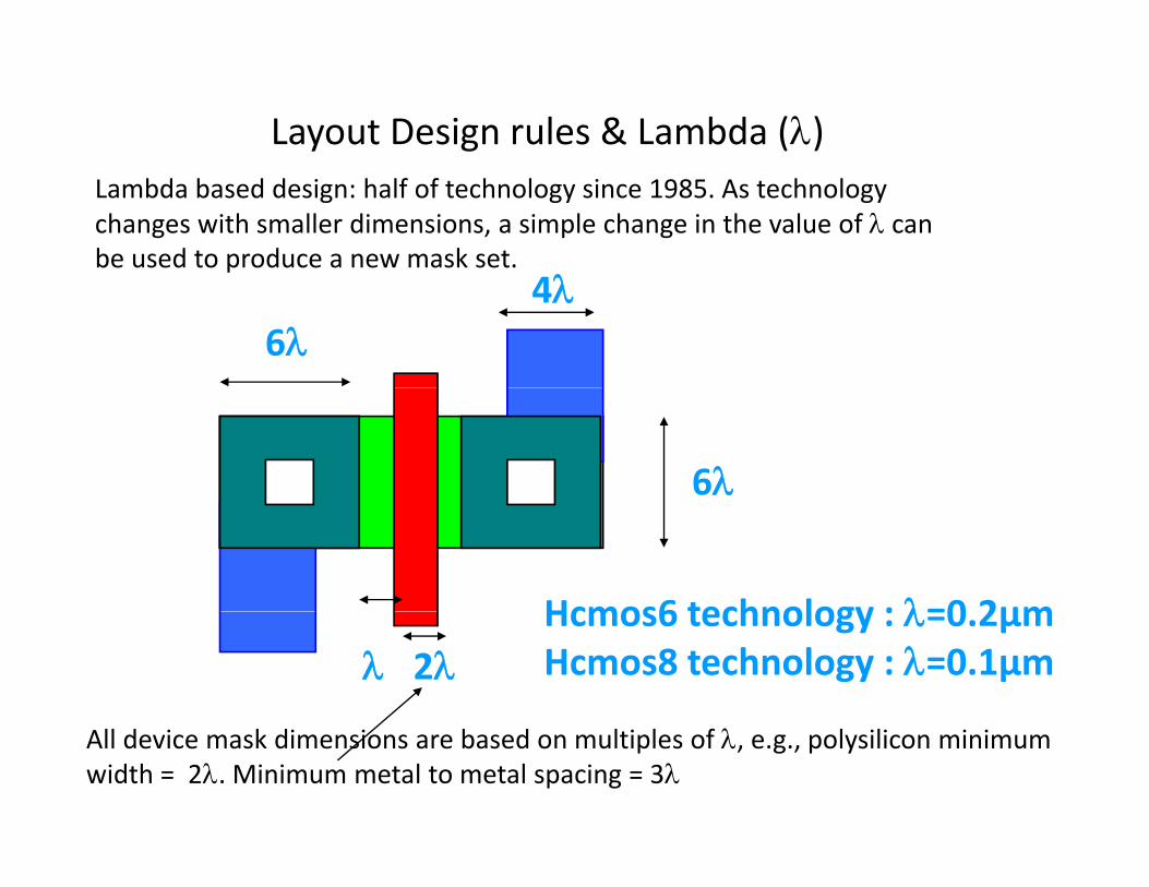
Layout Design rules & Lambda (λ)Lambda based design: half of technology since 1985. As technologychanges with smaller dimensions, a simple change in the value of λ canbe used to produce a new mask set.
λ6λ
4λ
6λ
Hcmos6 technology : λ=0 2µm2λλ
Hcmos6 technology : λ=0.2µmHcmos8 technology : λ=0.1µm
All device mask dimensions are based on multiples of λ, e.g., polysilicon minimum width = 2λ. Minimum metal to metal spacing = 3λ
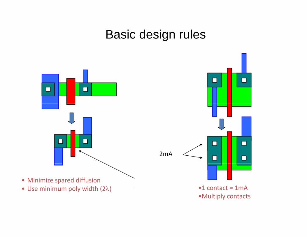
Basic design rules
2mA
• Minimize spared diffusion• Use minimum poly width (2λ) •1 contact = 1mA
•Multiply contacts
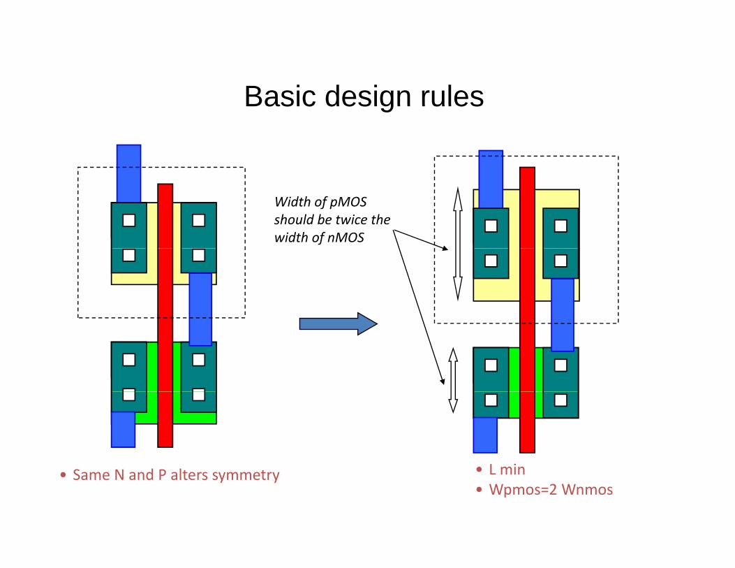
Basic design rulesBasic design rules
Width of pMOS should be twice the width of nMOS
• Same N and P alters symmetry • L min• Wpmos=2 Wnmos
nMOS transistor mask representation (See stick diagram next slide)for comparison
gatesource
polysilicon
drainsource
metal
Contact holes
diffusion (activeregion)
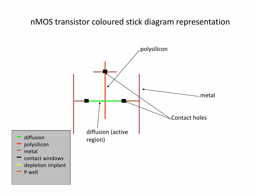
nMOS transistor coloured stick diagram representation
polysilicon
metal
Contact holes
diffusion (activeregion)diffusion
polysilicon metal contact windowscontact windowsdepletion implantP well
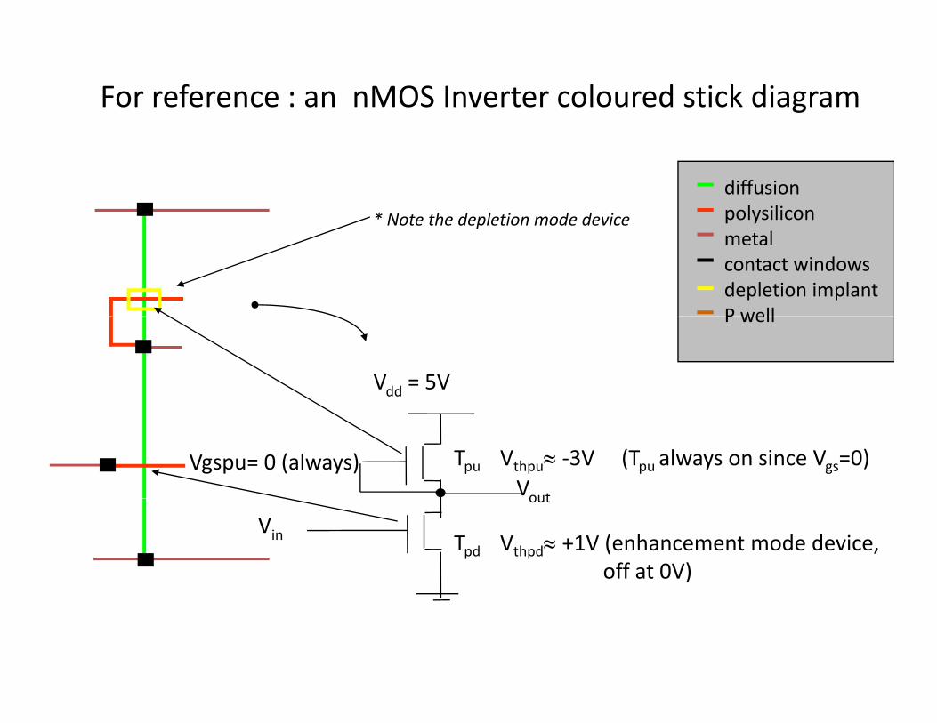
For reference : an nMOS Inverter coloured stick diagram
* Note the depletion mode device
diffusionpolysilicon Note the depletion mode devicemetal contact windowsdepletion implantP well
Vdd = 5V
P well
VoutVgspu= 0 (always) Tpu Vthpu≈ ‐3V (Tpu always on since Vgs=0)
out
Vin Tpd Vthpd≈ +1V (enhancement mode device, off at 0V)
CMOS Inverter Mask Layout
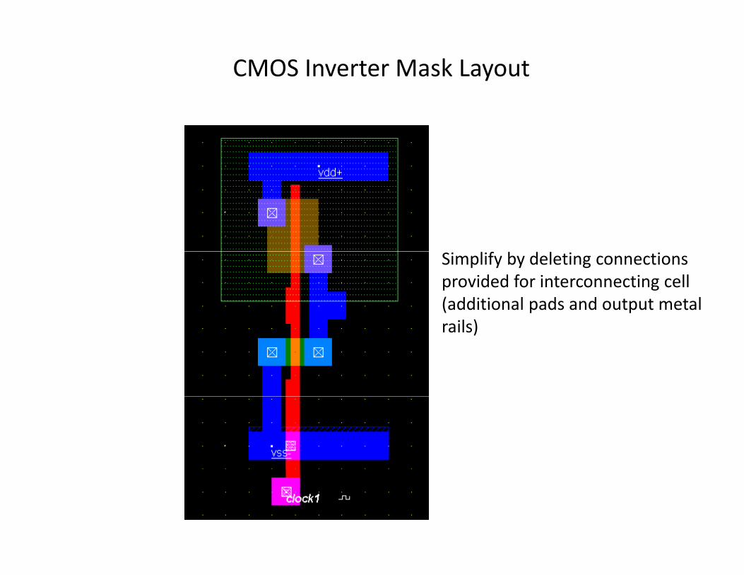
CMOS Inverter Mask Layout
Simplify by deleting connections provided for interconnecting cell (additional pads and output metal rails)rails)
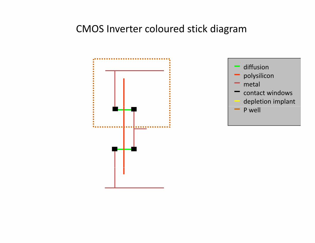
CMOS Inverter coloured stick diagram
diffusionpolysiliconpolysilicon metal contact windowsdepletion implantP well
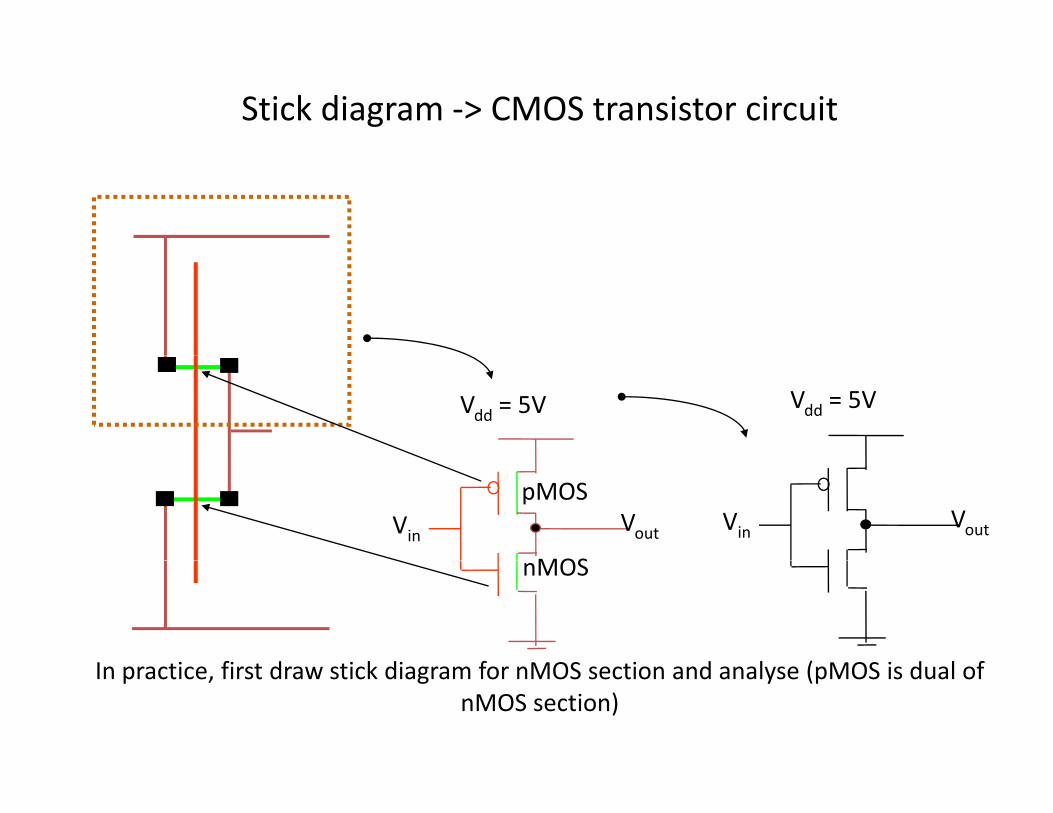
Stick diagram ‐> CMOS transistor circuit
Vdd = 5V Vdd = 5V
VoutVinVoutVin
pMOS
MOSnMOS
I i fi d i k di f MOS i d l ( MOS i d l fIn practice, first draw stick diagram for nMOS section and analyse (pMOS is dual of nMOS section)
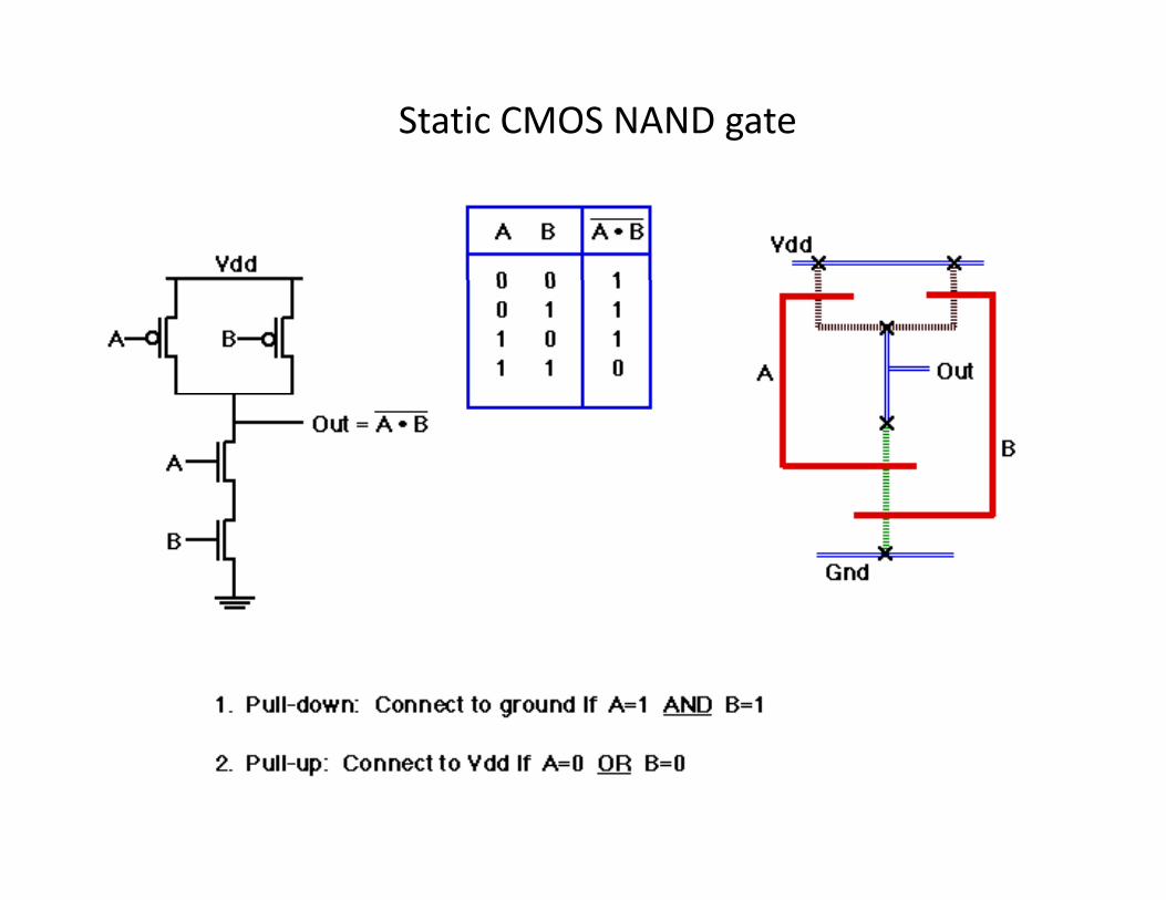
Static CMOS NAND gate
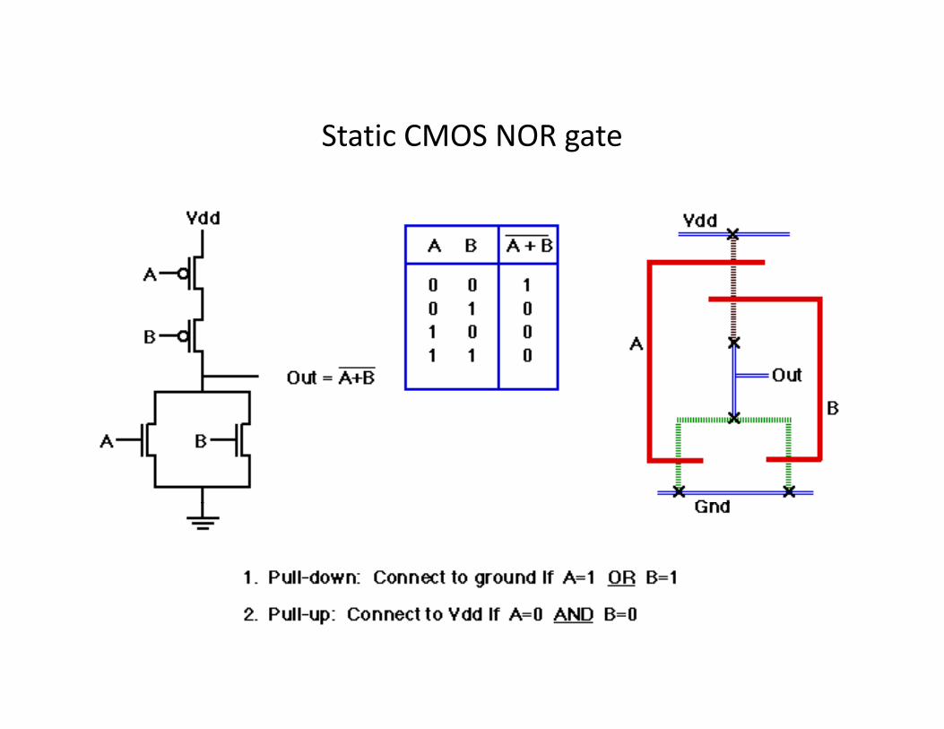
Static CMOS NOR gateStatic CMOS NOR gate
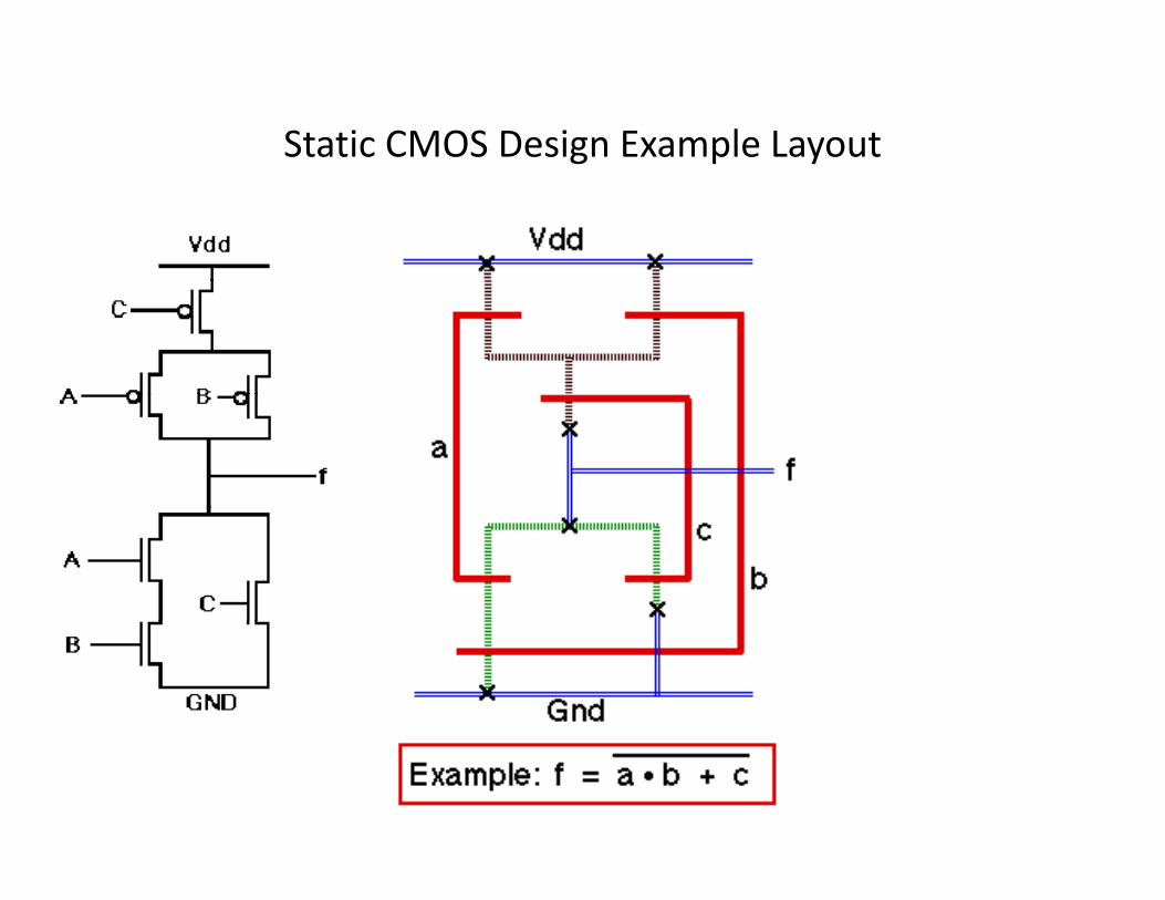
Static CMOS Design Example Layout
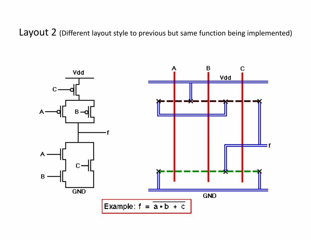
Layout 2 (Different layout style to previous but same function being implemented)
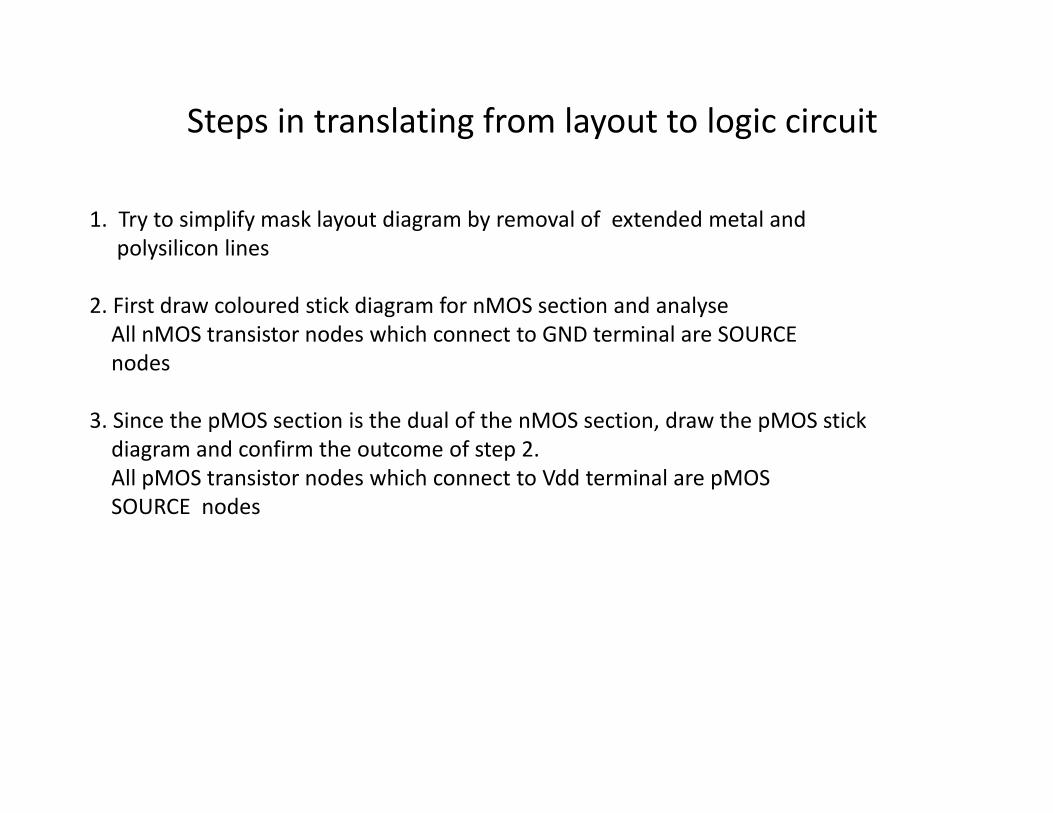
Steps in translating from layout to logic circuit
1. Try to simplify mask layout diagram by removal of extended metal and polysilicon linespolysilicon lines
2. First draw coloured stick diagram for nMOS section and analyse All nMOS transistor nodes which connect to GND terminal are SOURCE
dnodes
3. Since the pMOS section is the dual of the nMOS section, draw the pMOS stickdiagram and confirm the outcome of step 2.g pAll pMOS transistor nodes which connect to Vdd terminal are pMOS SOURCE nodes
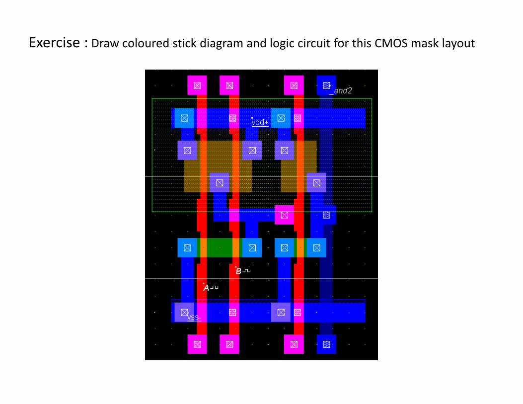
Exercise : Draw coloured stick diagram and logic circuit for this CMOS mask layout
Layout Design RuleLayout Design Rule
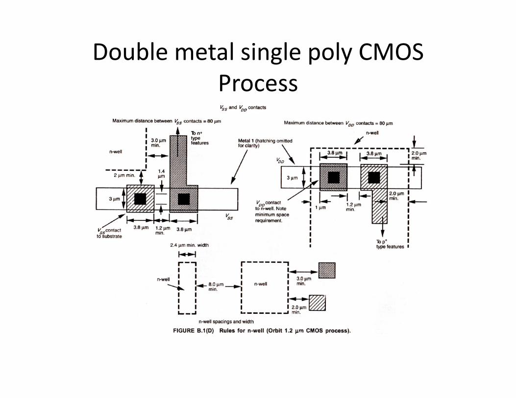
Double metal single poly CMOS Process